- Introduction
- Disclaimer
- Motivation of this work
- Manuals
- Fluke 510A AC standard review
- Overview of 510A design and internal construction
- How to calibrate Fluke 510A in hobby lab?
- Frequency setting PCBA modules, DIY manufacturing and design
- Safety precautions
- Measurement results with Fluke 510A
- Summary
Introduction
This is part 1 of the article series about AC metrology, AC Voltage standards and various experiments about this. This is summary of the 3.5 years’ experience in attempt to perform AC Voltage calibration problems for laboratory instruments. We will look on commercially available and obsolete instruments (and their modifications, sometimes quite elaborate), as well as building own AC Voltage artifact standards and devices.
There will be performance tests, schematics and sketches. PCB layouts are somewhat tricky, because first design is never good design, and author spent meters of wiring to correct layout routing and fixing routing errors. Engineer who say that their design work flawlessly from first try is the engineer who did not design complex system before :). Take the published designs as a starting point and not the finished polished commercially-valid design. All information provided below is for research purpose only.
Disclaimer
Redistribution and use of this article, any part of it or any images or files referenced in it, in source and binary forms, with or without modification, are permitted provided that the following conditions are met:
- Redistributions of article must retain the above copyright notice, this list of conditions, link to this page (https://xdevs.com/article/f510a_p1/) and the following disclaimer.
- Redistributions of files in binary form must reproduce the above copyright notice, this list of conditions, link to this page (https://xdevs.com/article/f510a_p1/), and the following disclaimer in the documentation and/or other materials provided with the distribution, for example Readme file.
All information posted here is hosted just for education purposes and provided AS IS. In no event shall the author, xDevs.com site, or any other 3rd party, including Fluke be liable for any special, direct, indirect, or consequential damages or any damages whatsoever resulting from loss of use, data or profits, whether in an action of contract, negligence or other tortuous action, arising out of or in connection with the use or performance of information published here.
If you willing to contribute or add your experience regarding instrument repairs or provide extra information, you can do so following these simple instructions.
Motivation of this work
Respected metrology scientists and calibration professionals who own or have access for modern high-end calibrators such as Fluke 57XX or Datron 4808 most likely will not be a target audience for this article. But it’s still very educational work and recommended to read thru.
However, many people who work with electronics design with limited budget already own and use great industry standard HP/Agilent/Keysight 34401A 6½-digit DMM. These DMMs are true workhorses and can be acquired cheaply, unlike fancy Fluke 5700A calibrator. It is great to buy properly working and traceable calibrated 34401A, as these DMMs usually stay well within specifications for years offering trouble-free performance and no blue-screens like modern LCD/Linux-based shiny instruments. But often these proven good instruments fetch higher prices, and after all one always want to know the answer to question “My meter is inaccurate, but how much inaccurate is it?”
As a side note, luck with secondary market for instrumentation can vary a great deal. I’ll never forgive myself missing a chance to buy “Power supply, DC source Fluke 732B” listed for $100 USD (yes, one hundred dollars!). This was before I knew about LTZ1000 stuff and I just did not know what Fluke 732B is exactly. After internet rectified lack of knowledge by same evening unit was gone gone gone. People who hunt for these standards know that good deals last barely minutes, if not seconds.
Also even if buyer found a deal in the right time, it must be also the right country. Often buying stuff from US or EU and trying to ship it to other country such as post-USSR one imply dealing with shipping restrictions and customs, paperwork and whatnot else involved. Sellers often don’t want any trouble, as there is a line of buyers in their own country already. Also even if I manage to get busted up instrument, full re-calibration and adjustment is a must after even minor repairs.
While doing calibration and adjustment of the 6½-digit DMM for DC Voltage resistance and DC current can be done using various references and resistance standards, AC Voltage and AC current has troublesome areas and challenges. There are some designs with microcontrollers which I’m afraid to touch due to lack of experience in embedded design. I’m not a software engineer in the slightest. AC sources that are easy to build are unable to provide good level of accuracy or stability required to even remotely satisfy calibration requirements for 6½-digit DMM.
I had a chance to buy used FLUKE 5200A but this would only solve sourcing up to 100 VAC levels. High voltage amplifier such as Fluke 5205 for this calibrator cost more than unit itself and also weights nice 55 kg and require three-person lift. Not the direction I wanted to take in modern years.
So what else we can find on ePay for query “AC Voltage reference/standard/calibrator/source” with price limit $100 USD or less? In December 2016 I have bought $68 USD Fluke 510A specified for 19200 Hz frequency. Exactly year later I got second unit for $65. Luck ran out afterwards, and hardships to establish AC Voltage artifact in lab began.
Manuals
Fluke 510A/AD instruction manual
Fluke 510A/AA instruction manual
Fluke 510A AC standard review
As instruction manual tells us, this device from 1990 era can be used as precision standard for AC Voltage with specified accuracy 100 ppm in 24 hours time period, or 150 ppm for 30 days for fixed frequency output (50, 60, 400, 1000, 2400, 5000 or 19200 Hz).
100 kHz version is much worse, at 400 ppm for 24 hours and 500 ppm for 30 days specification. Total Harmonic Distortion spec is less than 0.005% to 10 kHz and frequency stability rated for 500 ppm/month.
Frequency of the output is fixed by hardware, there are no switches or other simple ways to change it. Frequency is obtained by using special PCB assembly inside of the unit and replacing it require full re-calibration. Frequency can be only slightly adjusted with a trimpot within ±1% without any disassembly.

Image 1: Front side
Output voltage is 10 VAC RMS and maximum output current is 10 mA. There is indication LED to show overload condition.
Available options for Fluke 510A:
- Option 510A-01: Rechargeable Battery Pack.
- Rechargeable battery power
- Phase lock assembly to sync multiple standard (Fluke Model 510A/AD)
- Output distribution transformer for 400 Hz with 8 output taps, with reduced accuracy and loading impedance limits not less than 100 kΩ per output (Fluke Model 510A/AA)
- Frequency setting assembly for any of the settings per choice: 50, 60, 400, 1000, 2400, 5000, 19200 or 100000 Hz.
- Rack-mount kit set.
Unit is specified to meet performance limits with rather narrow ambient operation temperature +23 ±2°C window. Mains instability of ±10% would affect output for less than 10 ppm. Loading output change from 0 to 10 mA deviate output level less than 20 ppm for frequency options less than 10 kHz, and up to 80 ppm for 100 kHz unit. THD specified less than 0.005% for units less than 10 kHz, and up to 0.015% for 100 kHz.
Short term stability is less than 20 ppm peak, however manual shows plot with 1 Hz frequency band in 1 minute under 1 ppm. What to trust? We will test this later.

Image 2: Fluke 510A short-term stability plot from manual
Output amplitude temperature coefficient depends on output frequency and ambient temperature range, but specified from 5 to 22 ppm/°C.
Long-term stability is rated less than 500 ppm/month. Temperature coefficient for the output frequency is less than 150 ppm/°C. If unit calibrated against more precise DC Voltage reference, it’s possible to achieve better performance specifications.
Fluke 510A good enough to calibrate HP/Agilent 34401А at least on primary 10 VAC range?
To answer this question we need to check service manual for HP/Agilent 34401A.
Table on page 63 suggests 5 times better accuracy for calibration standard, compared to 24-hour specifications of the DMM under test. On page 14 in provided table we can see that 34401A achieves best accuracy on 10 VAC range in frequency band from 10 Hz up to 20 kHz and that is 400 ppm of the reading + 200 ppm of the range.
This means full-scale input voltage 10V (not 12V, which is “over-range”, outlined on page 22) stability of the DMM is ±(400+200) ppm = ±600 ppm. The sum of the contributors is confirmed on page 21 in same service manual.
As result required stability from calibration AC standard reference is 600 ppm / 5 = 120 ppm. Freshly calibrated Fluke 510A have slightly better limits at 100 ppm, but will be degraded more after a month period since last calibration to 150 ppm. However, there is a catch – these values only valid if Fluke 510A calibrated by its output AC Voltage signal. If we can calibrate and adjust 510A by using known to better than 15 ppm DC Voltage standard we can acquire performance less than 100 ppm for even 30-day period.
Based on this simple math we can say that Fluke 510A is suitable to calibrate HP/Agilent 34401A base 10 VAC range, with additional notes. These notes include:
- Full range of scaled AC voltages is required: 10 mV (1 kHz only), 100 mV, 1 V, 10 V, 100V and 195 to 770V for high voltage range.
- Full range of frequencies is required: 10 Hz on 10 V range, 1 kHz and 45-100kHz for high-frequency compensation adjustment
- 10mA AC current source is required with 1 kHz frequency.
AC High-current ranges like 1A and 2A are not adjusted in 34401A, but recommended to verify by manufacturer. This is bit different to HP 3457A requirements. I also have two HP 3457A DMMs, which were studied in this xDevs.com article
Further ideas:
- Voltage levels below 10 V AC we can acquire by using precision divider by 1/10/100/1000 build with non-inductive (not wirewound!) resistors. Excellent results are obtained using С5-61 foil resistors or VPG BMF resistors such as S102/VHP100/VHP200 series and alike.
- One of the buffered dividers with С2-29В 0.1% resistors used in future part of this articles series and show good results. Better dividers with С5-61 were built using standalone units and tested for good frequency response.
- 10 mA AC will be needed only for repairs involving components of AC functionality (pretty common for old 34401A) or after replacement of the CALRAM U505 (rare cases). It’s possible to work around this case using single non-inductive reference resistor 1000 Ω (or from 900 to 1100 Ω characterized to 6 or more digits) and simple Ohm law math. But this is reduced accuracy/uncertainty method.
Obviously for best results direct verification against traceable standard is required.
Firmware upgrade of the HP/Agilent 34401А can alter or erase CALRAM data. I’ve had this problem already, beware!
Overview of 510A design and internal construction
Fluke 510A outputs stable 10 VAC RMS. Take a look on block diagram from instruction manual to study how this instrument create stable AC voltage output.

Image 3: Fluke 510A simplified block diagram
Alternating voltage is generated by output operational amplifier which have two feedback loops. One loop is frequency-dependent negative feedback with half of the double T-bridge connected to inverting input of the “opamp” and frequency-independent positive feedback loop on non-inverting “opamp” input. Opamp here is merely a functional term, because in Fluke 510A this amplifier block is built using 10 discrete transistors and occupy half the available PCB space.
T-network bridge in this circuit allows rejection of all frequency content except desired resonant frequency tone. T-network works like parallel oscillation loop providing maximum impedance on the resonance frequency. If signal frequency differs from this resonant frequency the effective impedance will be much less. And with connection between output and inverting output of the amplifier all non-desired frequency signals will be cancelled out. And vice-versa resonant frequency will not be routed to non-inverting input and will not be affected.
Other requirement is tightly controlled positive feedback to obtain oscillation. This feedback is responsible for maintaining stable amplitude of the output signal. Set point in this loop is variable resistance of the FET channel in front of the amplifier/oscillator.
Other than output terminals output signal is also routed to peak detector. This peak detector is used to generate proportional voltage level to negative amplitude of the reference DC voltage, which is carefully selected 14.14212 VDC. This is important piece of the AC standard, let’s clarify why. There is 1:1:1 ratio divider, one of only three precision selected components that determine whole instrument performance and stability. This divider built with series connected resistors of equal value and matched for temperature coefficient combined onto same package. Middle point of the divider connected to opamp with low input bias current.
One of the divider inputs supplied with fixed 14.14214 VDC, which is obvious square root of the value 2 multiplied by 10. What is the relation between RMS and amplitude of the AC voltage? Yes, amplitude is SQRT times larger than RMS output value.
What we got at the output of this divider circuit? We got large portion of the reference voltage at the output. Now going back to our peak detector. It will not detect any positive voltage, which we can guess by looking at the diodes between input to output (which is not present in hardware). Anyhow it’s not important, what is important – peak detector works only with negative voltages, but our reference is positive.
And before voltage transitions to negative levels we reach zero voltage crossing. Also don’t pay attention to circle detail drawing showing nice sine-wave with +14.14214 V, it’s actually misleading. Only negative half-wave section of the signal matters. Also mains transformer on block diagram is not show, it is indeed present in the instrument, allowing operation in mains with 115V or 230V level and frequency from 50 to 500 Hz.
So how we get to zero voltage at the middle point of the divider? We can supply on remaining input (divider has 3 nodes) voltage equal to the reference voltage but inverted. So if we get positive voltage, then remaining input should get negative reference voltage.
If we get opposite voltage fraction larger, then output of the divider will reach polarity of the larger (by amplitude) voltage and in this case it will become negative. Negative voltage will be inverted by peak detector as result, amplified and with sample-hold circuit and integrator (which is NON-inverting here, meaning lower input voltage will get larger output). Result will be fed to gate of the FET we briefly mentioned above which sets the feedback correction. Biasing FET will result in lower channel resistance and weaker feedback action. Which in result cause lower output voltage.
This is how whole loop works and sample-hold circuit needed here because more than 97% of the peak detector duty time is off with positive voltage from the input of the reference voltage source, and active only during 20-30 microseconds when signal reach of the negative maximum section of output sine signal (equal to or microvolts higher reference voltage). Remaining 97% of the time sample-hold circuit will maintain stable DC voltage on FET gate till next sine wave maximum will be reached.
Interesting to estimate how much higher output amplitude can be over reference voltage. In manual on page 1-2 we have best stability for 24 hours at 20 ppm. This means that Image 2 with example 1 min plot is misleading and actual measured instability at 1.6 ppm peak to peak.
It is intuitive that peak detector must have sensitivity much better than instability specifications. We entered murky waters of estimations, but perhaps 10-fold sensitivity margin wouldn’t be too optimistic here, if one to remember than 1.6 ppm peak value was during 1 minute time frame. Peak detector using LM308 opamp which has typical gain of 300000. Also we have differential cascade build with discrete parts at the input of the amplifier, further increasing total gain by few magnitudes (differential input stage only need to have gain around 7 for this, relatively easy task).
Going further, pulse amplitude at the peak detector should be few hundred millivolts to work. If we divide this amplitude even just by 1000000 we get few hundred nanovolts, which is still optimistic figure. If this is not correct, feel free to let me know. If we go back to stability spec, we get figure about 0.16 ppm from 14.14214 V reference, which is 2.26 µV. This would be pessimistic estimation. As result real signal that peak detector operates with somewhere between these pessimistic and optimistic levels, meaning from few hundred nanovolts to few microvolts.

Image 4: Measured oscillogram of the negative sine peak pulse at peak detector
After this feedback loop maintains voltage at the input of the peak detector not more negative than reference level. If voltage on the input of the peak detector never cross zero level pulses will not be generated and sample hold circuit will be slowly discharging, which will cause control FET to close up and result in increased feedback, meaning increasing of the output voltage AC level. Integrator circuit parameters define dynamic performance of the system such as rise and fall times of the FET gate voltage.
Power supply in Fluke 510A generate +18 and -18 VDC, and reference voltage for positive rail is negative -18V. In return reference voltage for negative PSU rail is the very same voltage reference used in peak detector circuit, which is powered by? Positive +18 VDC from power supply! Not bad of the loop, eh? Turn on process of this circuit resemble story of Baron Munchausen, who pulls himself and his horse from a swamp by pulling hair on his own head. :)
What else is there in 510A? Sure, overload indicator. This is very complex circuit consisting of resistive current sensor, few parts and whole ONE transistor with LED, which should turn on if output current exceed 10 mA. Actual threshold level is bit higher at about 12-13 mA, as divider at the peak detector is using about 1 mA plus some extra for losses in transistors.
Mains transformer is installed on the bottom from the main PCBA, closer to the rear side of the unit.
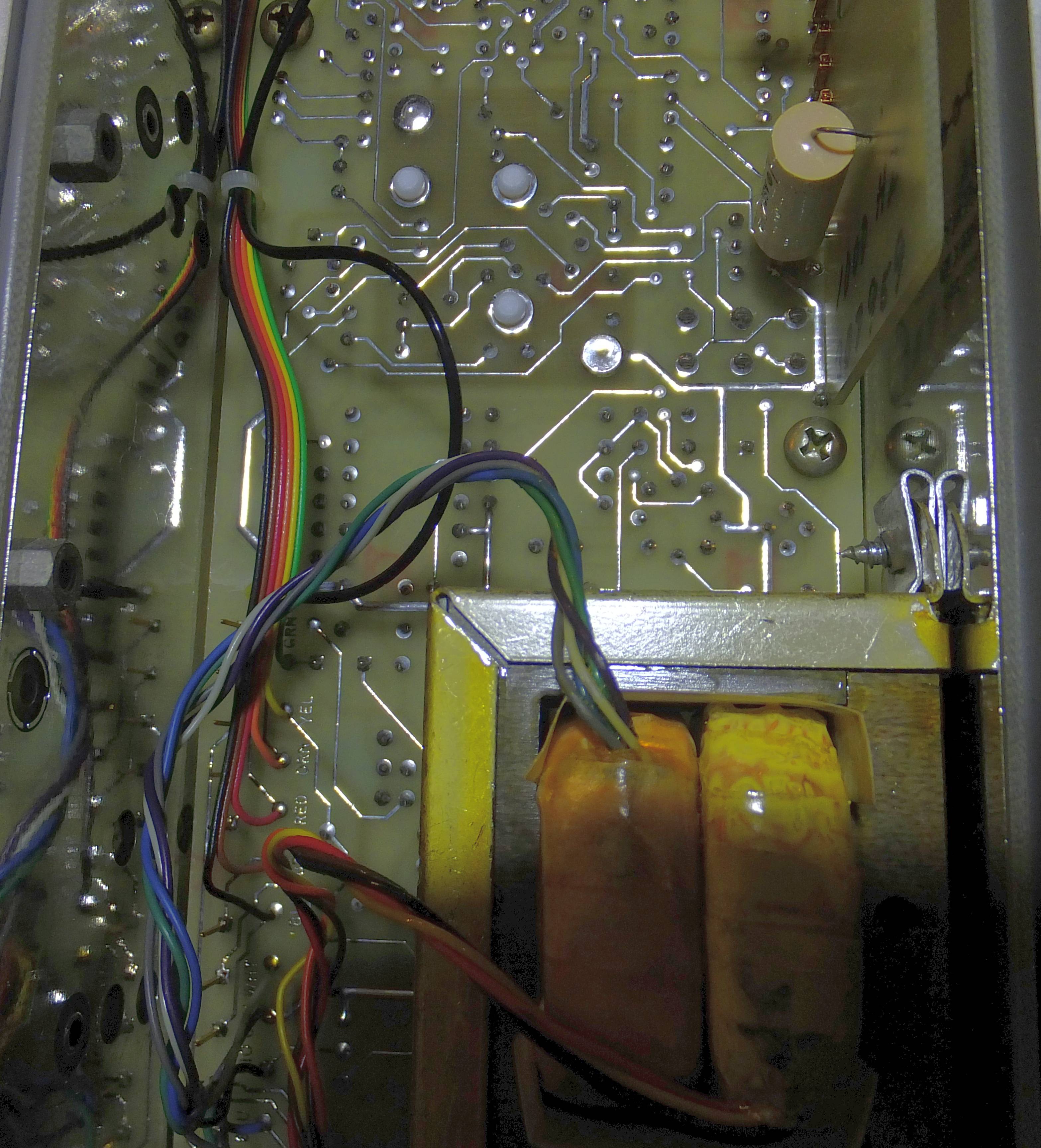
Image 5: Power supply and peak detector board, bottom
Power supply is located on the same main PCB above the transformer.

Image 6: Power supply
Pay attention to shielding on the sides, made out of double-layer FR4 PCB. Conductive surface of both sides is isolated and aluminum case might hint for triple shielding. But no, outer side of the inner shield is connected to the chassis, so it’s only dual-shielding here in 510A.
If we move from rear side of the board to front, we see peak detector and voltage reference circuit.

Image 7: Overview photo
Voltage reference has two remaining high precision components, one of which is mighty Motorola SZA263, also used in Fluke 732A, older Fluke 5700A and some other Fluke instruments from that era. List of Motorola SZA263-based voltage references used by Fluke shown in table below.
| Fluke 341A DC Voltage Calibrator | Fluke 5440B DC calibrator – two SZA263 chips |
| Fluke 343A DC Voltage Calibrator | Older Fluke 732A DC Voltage Standard |
| Fluke 515 Portable calibrator | Fluke 731B DC Voltage Standard |
| Philips PM2530 7½-digit DMM | Fluke 5520A Multi-function calibrator |
| Fluke 8840A 5½-digit DMM | Fluke 5522A Multi-function calibrator |
| Older Fluke 8842A 5½-digit DMM |

Image 8: Voltage reference
SZA263 has related resistive network which determine temperature coefficient of the voltage reference output.

Image 9: Voltage reference and precision resistor network
Because peak detector must work with signals less than microvolt it has own shielding (top cover, removed during photo-shoot for clarity) and solid copper pour on bottom side of the PCB. With red arrow marked that 3-resistor divider we talked about earlier.
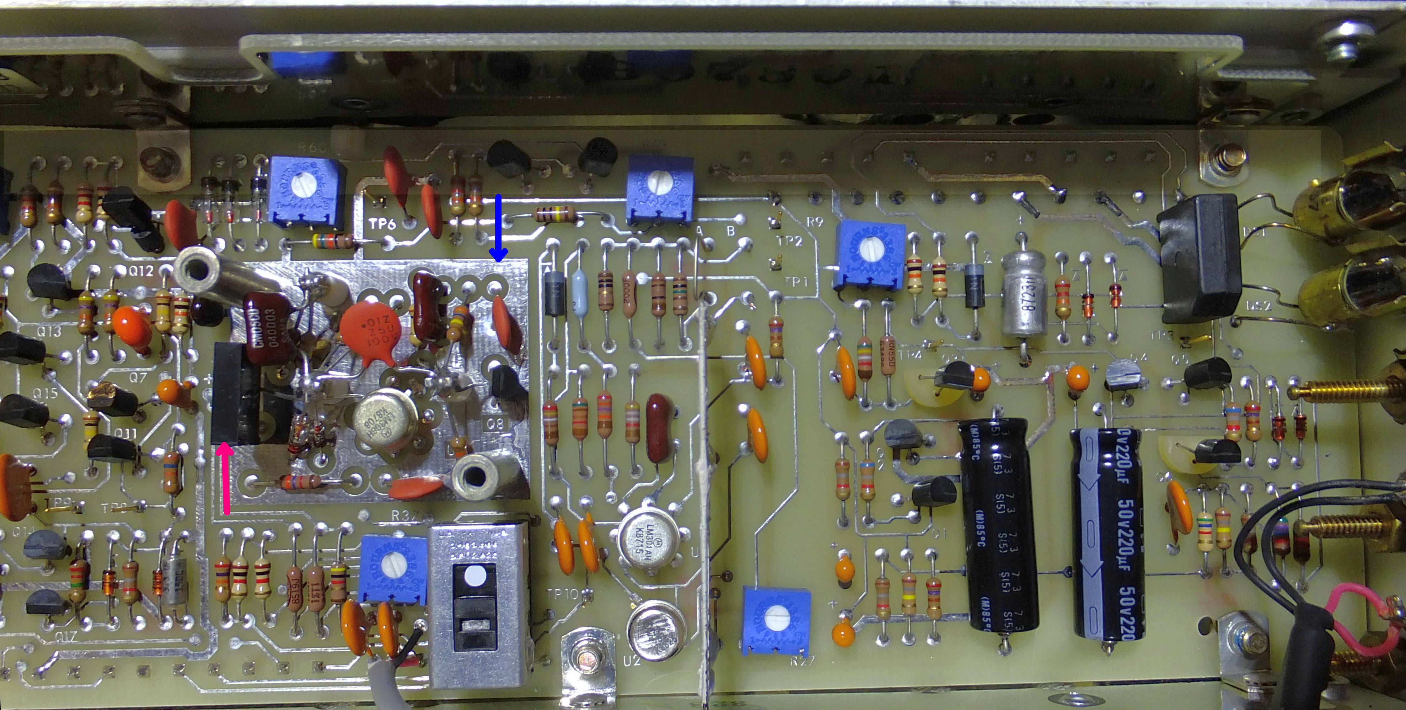
Image 10: Peak detector and power supply
Removable frequency setting PCBA (also with Fluke part number) is installed on internal shield under main PCBA. Electrical connections to mainboard implemented using 19 pin-collect contact with 5.08 mm pitch. It will be important design requirement for later.

Image 11: Bottom side
Image 12: Rear panel

Image 13: Side panel

Image 14: Bottom panel
This is enough on this stage as teardown and theory of operation. Let’s take a look on calibration procedure for 510A standard.
How to calibrate Fluke 510A in hobby lab?
What was the main reason to buy Fluke 510A? Unlike many other devices this AC reference standard can be relatively simply calibrated with limited set of tools.
- Oscilloscope (2 channel is nice, but not required).
- Frequency counter (Integrated into oscilloscope in my case, but any digital counter will be fine).
- 5 or 6½-digit DC Voltmeter (HP/Agilent 34401А adjusted and calibrated on DC Voltage ranges).
- DC Voltage source or calibrator capable to source stable 14.14214 VDC with uncertainty less than ±15 ppm (upgraded Fluke 343 or even fixed purpose DIY LM399/LTZ1000A module)
- Null-meter such as Fluke 845AB/AR or Keithley 155 nice to have, but not required. HP3456А or good HP/Agilent 34401A with stable zero readings can be used here.
HP3457А is not suitable as null-meter, it’s too noisy. Fluke 8842A might also work due to extended 20 mV DC range, but I didn’t test this.
That’s it! Fluke 510A calibration adjustment does not require ultra-stable thermal converters, locking detectors, AC Voltage standards or anything else related to very expensive AC voltage metrology.
Fluke 510A Calibration adjustment sequence
Before doing any adjustments or calibration tests power up 510A and let it warm up during few hours (manual suggests only 10 minutes).
Connect DMM between test point TP2 (Image 15, red circle) and common (same image, blue circle). Use trimpot resistor R9 (red arrow) to adjust +18 V power supply voltage within ±0.2 V. In my experience it’s better to set voltage slightly higher to get better margin for amplitude, which is not bad to have. In my units I set even higher, around +18.5-18.8 VDC but here +18.20 VDC will be good point.

Image 15: Positive power supply adjustment
Now test voltage on the test point TP4 (yellow circle) to make we got -18.0 VDC within ±0,5 V.
Voltage reference adjustment
This part is most challenging in calibration adjustment. We cannot directly measure +14.14214 V level with HP/Agilent 34401A with base range 10V (12V with overflow). Higher voltage range 100V will load up output with DMM’s 10 MΩ input divider and will cause large error in reading. Ideal would be to use DMM with full-scale 20V such as Keithley 2002, Datron 1281 or similar, but I have only Keithley 2001. My K2001 has temperature coefficient around 1 ppm/°C, so it’s quite tricky to measure voltage reference with it. Fluke 8842А does not have required resolution. So more cumbersome way required here.

Image 16: Schematics of VREF adjustment step
Image 16 show DIY device with voltage reference with matching output voltage +14.14214 VDC (did you memorize this magic value already? I did, even more precise 14,142135 VDC). Then with well warmed up null-detector set in best sensitivity mode (6 DIGIT 100 NPLC for HP3456А or SLOW 6 DIGIT for HP34401А) we remove zero offset.

Image 17: Copper shorts for zero offset calibration
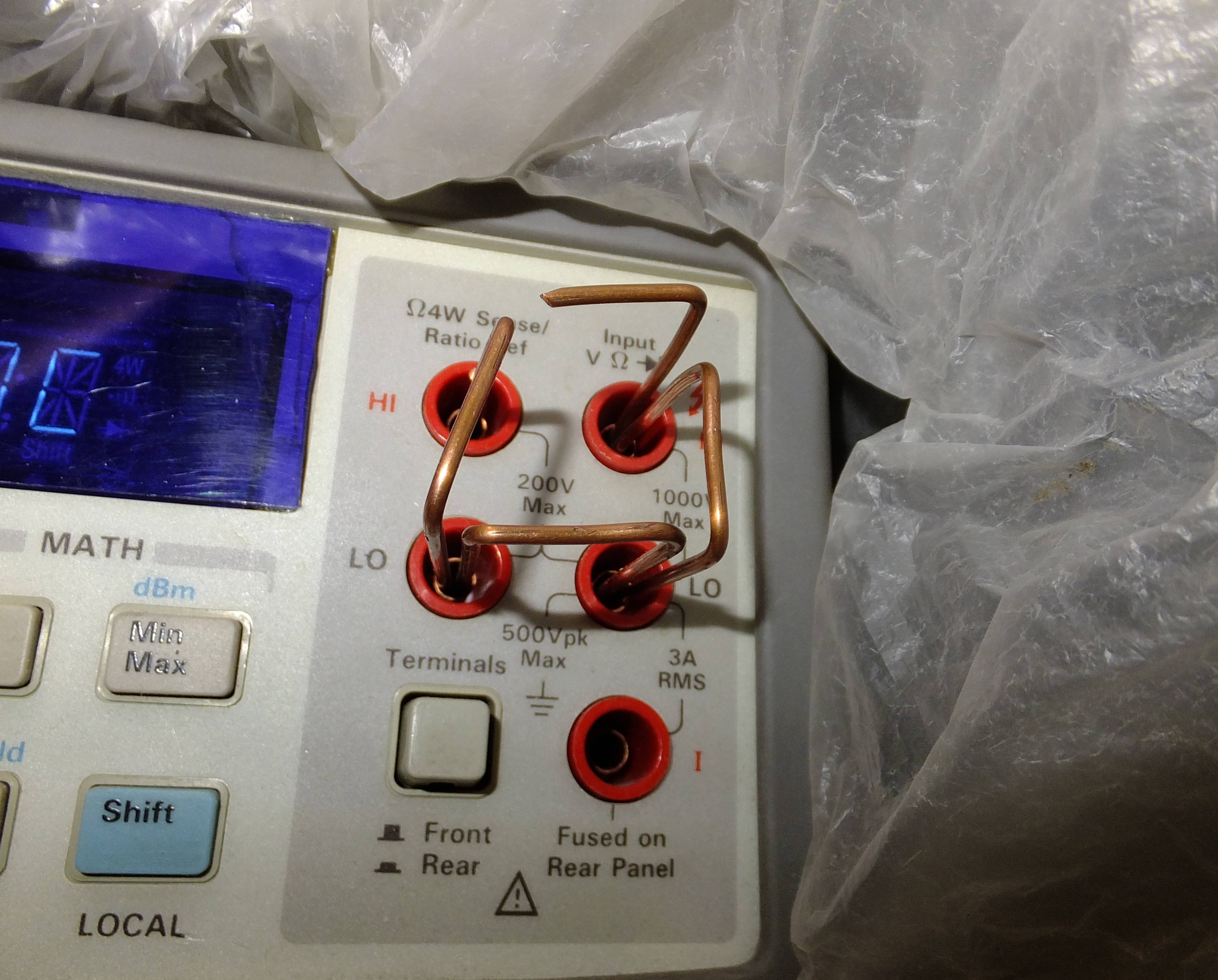
Image 18: Copper short installed in HP 34401A
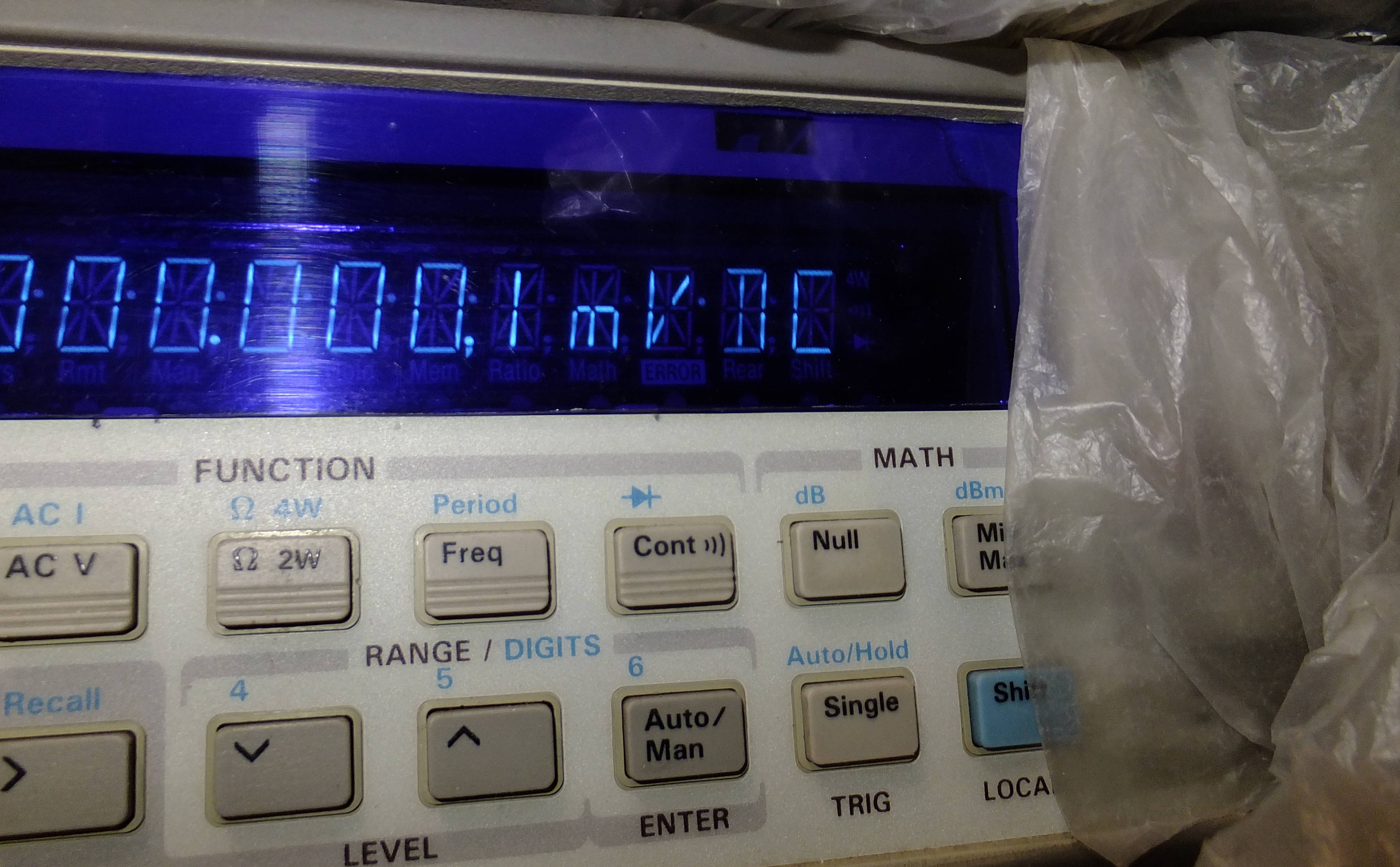
Image 18b: Measured zero
To do this I used fresh clean copper wire (shown on Images 17-18b) inserted directly to DMM input terminals. For DMM that does not have zero calibration (such as HP3456A or Fluke 8842A) use relative mode on lowest DC voltage range with zero short installed.
Now negative of the reference voltage module we connect with peak-detector shield (blue circle on Image 18) with copper wire without any tin coating or connectors. This is important not to introduce unwanted metal junctions to keep thermal EMF to minimum. Positive output of reference voltage module connects with same wire to negative terminal of the null-meter. HI positive terminal of the null-meter connect to test point TP10 in 510A (red circle on Image 19). Let everything settle for 15 minutes to reach thermal equilibrium.
Adjust trimpot R27 (red arrow on Image 19) for minimum deviation between external reference and 510A voltages. Ideally to keep difference less than 50 µV.
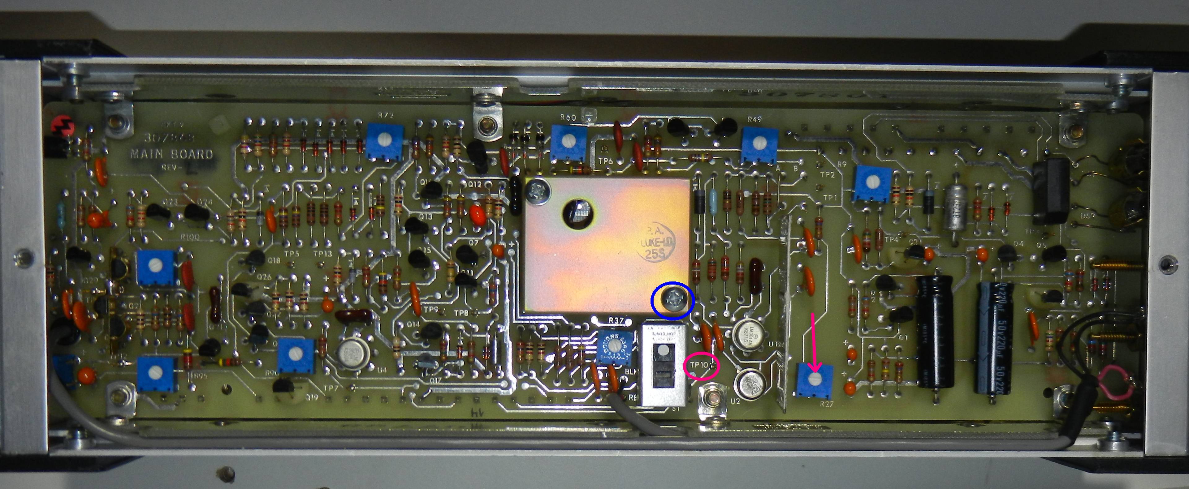
Image 19: Calibration points and trimpot location for VREF adjustment
Quiescent current adjustment
Despite procedure in 510A manual in next step I adjust quiescent current of the output 2.5 mA stage. For this we need to halt oscillations by shorting test point TP13 (yellow circle on Image 20) to common (shield of the peak detector). Negative LO from voltmeter DMM connect to TP4 (blue circle on Image 20), positive HI to test point TP11 (red circle on Image 20)
Adjust trimpot R100 (red arrow on Image 20) until +0.25 V obtained on the DMM.

Image 20: Quiescent current points and trimpot locations
Disconnect DMM and remove short from test point ТР13. Let 510A powered on and settle for 15 minutes to stabilize.
Bias current for feedback FET
Connect LO of the voltmeter to common (shield of the peak detector, blue arrow on Image 21) and HI input to test point TP5 (red circle on Image 21).
Adjust R90 (red arrow) to obtain -2.5 VDC ±0.2 VDC reading.

Image 21: Bias current adjustment points
Balancing peak detector operation and integrator adjustments
Keep LO from DMM connected to same shield point.
For peak detector calibration adjustment connect HI input from DMM to the test point ТР6 (red circle on Image 22).
Adjust R49 (red arrow on Image 22) to obtain zero volts ±100 µV.
For integrator calibration adjustment connect HI of the DMM to TP7 (yellow circle on Image 22). Keep LO at the shield.
Adjust R72 (yellow arrow on Image 22) to obtain zero volts ±100 µV. In my own designs I used only multiturn adjustment resistors and had no problems to obtain zeros here less than ± 30 µV.
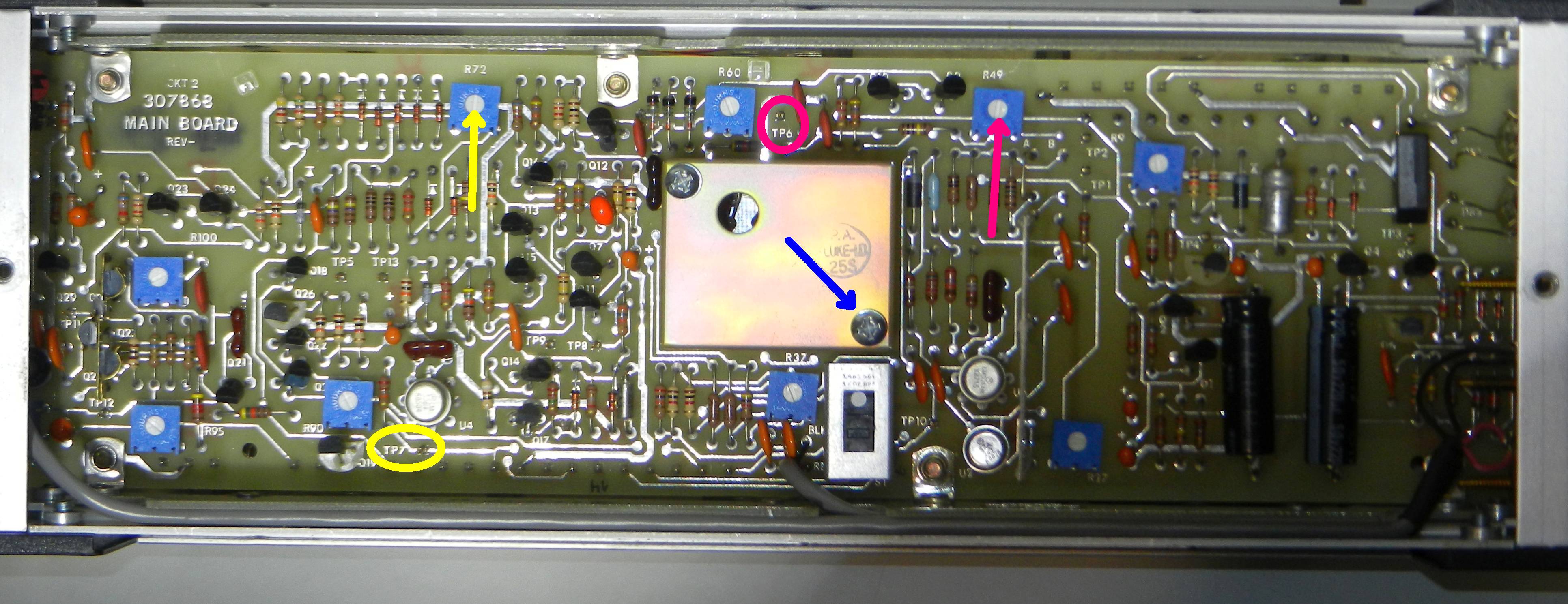
Image 22: Integrator and peak detector adjustments
Disconnect DMM.
Detector threshold adjustment
With my multichannel oscilloscope this adjustment was done following next procedure.
Connect output of the Fluke 510A (level 10 VRMS) to channel 1 of the oscilloscope. Set trigger to falling edge of the signal and adjust oscilloscope gain and waveform position to see negative sine maximum with best resolution (example shown on Image 2). Second channel of the oscilloscope connect thru 1:10 attenuator to test point TP8 (red circle on Image 23). All further adjustments on scope will be done this this channel 2.
Warning! In this configuration DO NOT connect attenuator’s common anywhere to avoid ground loop thru the scope.
Now following manual’s recommendations adjust sensitivity on channel 2 to 10 mV/div level. Terminate input to ground and set signal level to middle of the waveform screen. Now select input from attenuated TP8 and check pulse signal. Peak of the pulse must be one division higher than middle zero level of the waveform graticule. Both of my 510As show 2.5 divisions pulse amplitude, and I followed same value in my designs, but manual tells only SINGLE division.
Adjust R60 (red arrow on Image 23) to get pulse amplitude correct.

Image 23: Oscilloscope probe points
If you have only single-channel oscilloscope, then perform this adjustment using method outlined in the manual.
Comparator balance adjustment
This is how it’s called in the manual. But I think it is peak detector input divider balance adjustment because comparator is nowhere to be found in schematics descriptions and not visible under any possible eye aid.
Connect best available DMM in AC Voltage measurement function to the output of the Fluke 510A with good quality short coaxial cable. HP3456A or HP/Agilent 34401A will work, but it’s better to use something nicer. Configure DMM to best sensitivity and precision for AC voltage measurements. Set lowest frequency digital filter.
Allow readings to settle and enable relative mode (NULL for 34401А or MATH NULL for 3456A/3458A. Set switch S4 (red circle on Image 24) to opposite position and obtain voltmeter readings.
Adjust R37 (red arrow on Image 24) until difference between both S4 switch positions is less than 50 µV which is 5 ppm.

Image 24: Balance adjustment for AC Voltage output
After adjustment switch S4 back to position marked with white dot.
Output frequency adjustment
Most useless or even harmful adjustment step. Attempt to obtain “perfect” round numbers like 1000.000 Hz will cause poor rejection with mains frequency tones and negatively affect output performance. So if frequency cannot be adjusted to desired value from the front panel port, this adjustment can help.
Connect frequency counter, adjust trimpot on front panel to middle point and adjust R95 (red arrow on Image 25) closest to desired frequency value.

Image 25: Frequency adjustment point
This adjustment can have effect on peak detector operation, because T-network points slightly change. It is good practice to readjust peak detector and integrator calibration adjustments as result.
Now Fluke 510A is calibrated and we got stable AC Voltage source with one fixed frequency. But remembering HP/Agilent 34401A DMM requirements we need not one but three frequency artifacts! Time for next step.
Frequency setting PCBA modules, DIY manufacturing and design
Working on this 510A unit and designing own versions of boards, I found a way to do replacements for frequency boards without redoing whole calibration for the output. With very careful and patient adjustment even coarse frequency adjustment pot R95 does not require trimming. Let’s not forget that tolerances for calibration voltages vary a lot from wide±10% for 10 Hz and 1 kHz to huge +122% (for outputs from 45 kHz to 100 kHz).
But we will talk about adjustment in next chapter dedicated for calibration procedures. First need to build and test frequency setting boards. This is the way :).
Required parts for building own frequency modules/boards listed below
- PCB FR-4 material with double-sided copper cladding
- Chemicals to etch and transfer layout artwork onto PCB
- BOM for components, referenced from the Fluke 510A manual. Non-standard frequencies calculated by ratio.
- Decent capacitance meter with ranges from picofarads to thousands microfarads (used Tektronix TX3, but later added infamous DE5000 и XJW_LCR_3.0)
- Resistance meter with 5½-digit or higher scale (used HP3456А, Fluke 8842А, HP34401А but also can use 3457А, 8840А, etc)
To make a board I did not draw schematics but just took a ruler and made layout in PCB editor. Board is fairly simple, as you can see on images 27 below.
Modifications compared to original design involve wider PCB traces and added flexibility: most of thru-hole component footprints duplicated with SMT-type footprints. Also footprints for thru-hole capacitors have multiple holes to allow different pin pitch components. Pads also placed on both sides of the PCB.

Image 26: DIY frequency setting board for 510A
TEKTRON’s frequency mod board, TOP layer, PDF artwork
TEKTRON’s frequency mod board, BOTTOM layer, PDF artwork


Image 27: PCB layout artwork, both layers
It does not look very pretty, but I had to reinvent connector sockets since I did not have proper connectors for dual terminals.

Image 28: Connector sockets
First PCB modules were built on dual-sided FR-4 with desoldered sockets from old cables. These sockets were mounted directly on PCB pads and routing was done on opposite bottom side.
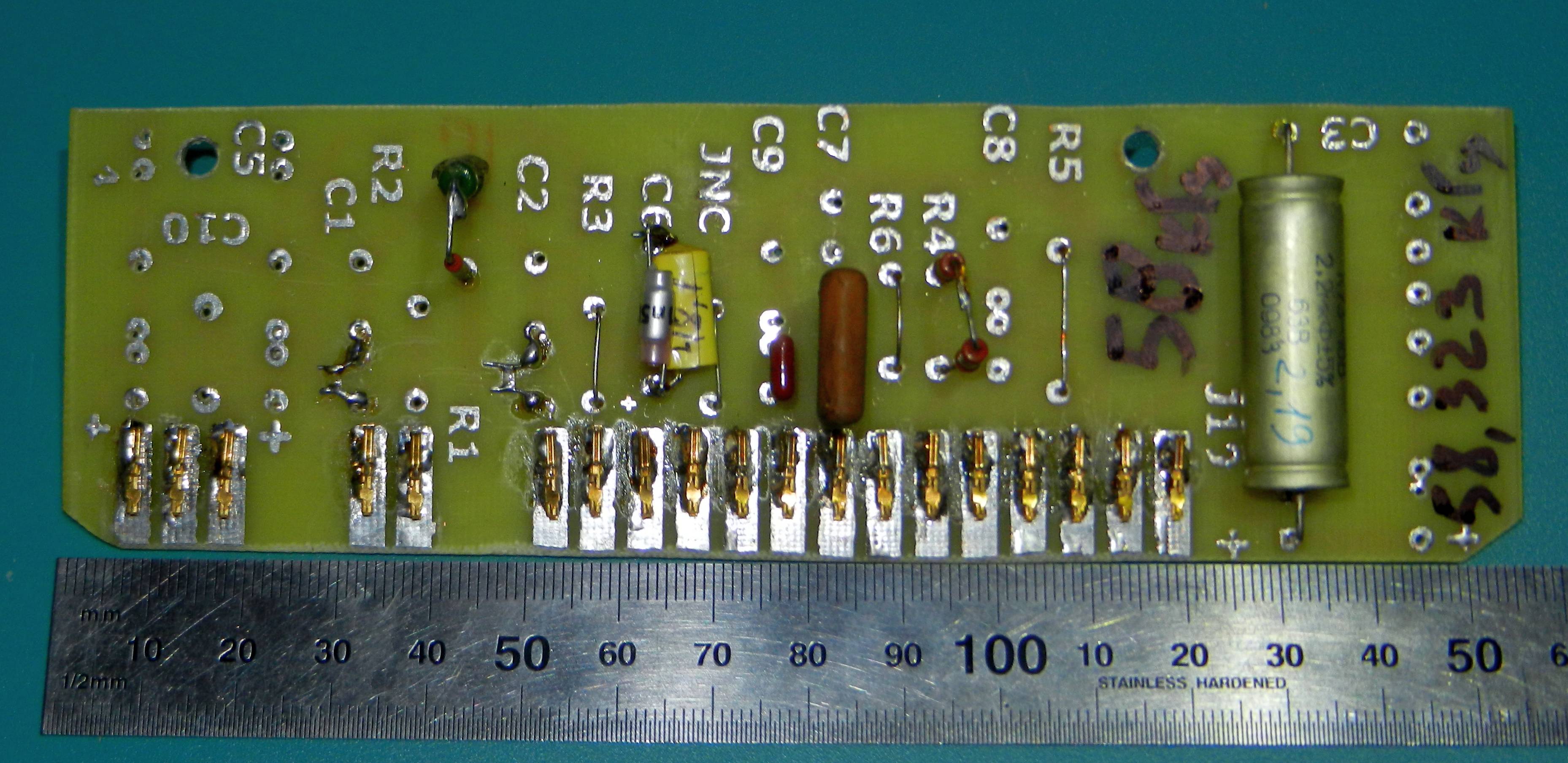
Image 29: Soldered joins on the bottom side of the PCBA
On later revisions proper connectors were purchased and PCBs were simplified for single-layer design.

Image 30: Improved PCB with single-sided copper routing

Image 31: More assembled frequency boards
BOM for calculated components, depends on desired output frequency on the Fluke 510A unit.
| FREQ Hz | 10 | 20 | 50 | 60 | 120 | 200 | 400 | 1k | 2k | 2k4 | 5k | 10k | 19k2 | 20k | 50k | 55k | 65k | 100k |
|---|---|---|---|---|---|---|---|---|---|---|---|---|---|---|---|---|---|---|
| C1’,C2’ | 1.35µ flm | 680n flm | 270n flm | 270n flm | 135n flm | 68n flm | 33n flm | 15n flm | 6.2n flm | 6.2n flm | 3n flm | 1.5n | 750p | 750p | 300p | 270p | 210p | 150p |
| C3’ | 1650µ Ta | 1000µ Ta | 330µ Ta | 330µ Ta | 330µ Ta | 15µ flm | 5µ flm | 2µ flm | 1µ flm | 1µ flm | 1µ flm | 1µ flm | 1µ flm | 1µ flm | 1µ flm | 1µ flm | 1µ flm | 1µ flm |
| C4’,C5’ | 1100µ Ta | 1000µ Ta | 220µ Ta | 220µ Ta | 220µ Ta | 100µ Ta | 68µ Ta | 68µ Ta | 68µ Ta | 68µ Ta | 68µ Ta | 68µ Ta | 68µ Ta | 68µ Ta | 68µ Ta | 68µ Ta | 68µ Ta | 68µ Ta |
| C6’ | 28µ Ta | 14µ Ta | 5.6µ Ta | 5.6µ Ta | 5.6µ Ta | 4.7µ Ta | 3.3µ Ta | 2.2µ Ta | 680n | 680n | 330n | 130n | 68n | 68n | 50n | 50n | 50n | 50n |
| C7’ | 2.35µ flm | 1.2µ flm | 470n | 470n | 470n | 100n | 50n | 50n | 50n | 50n | 50n | 50n | 50n | 50n | 10n | 10n | 10n | 10n |
| C8’ | 125n | 68n | 25n | 25n | 12n | 6n | 3n | 1.2n | 510p | 510p | 220p | 130p | 68p | 68p | 0 | 0 | 0 | 0 |
| C9’ | 0.5µ | 220n | 100n | 100n | 100n | 100n | 10n | 10n | 10n | 10n | 10n | 10n | 10n | 10n | 10n | 10n | 10n | 10n |
| C10’ | 0.5µ | 220n | 100n | 100n | 100n | 0 | 0 | 0 | 0 | 0 | 0 | 0 | 0 | 1 | 0 | 0 | 0 | 0 |
| J9-J17 | N | N | N | N | N | N | N | N | N | N | N | N | N | N | Y | Y | Y | Y |
| R1’ | 2.67k | 2.67k | 2.67k | 2.21k | 2.21k | 2.67k | 2.67k | 2.43k | 2.43k | 2.43k | 2.43k | 2.49k | 2.49k | 2.49k | * | * | * | 2.26k |
| R2’ | 42.2k | 42.2k | 42.2k | 34.8k | 34.8k | 43.2k | 43.2k | 39.2k | 39.2k | 39.2k | 39.2k | 39.2k | 39.2k | 39.2k | 36.5k | 36.5k | 36.5k | 36.5k |
| R3’ | 48.7k | 47k | 47k | 47k | 47k | 0 | 0 | 0 | 0 | 0 | 0 | 0 | 0 | 1 | 0 | 0 | 0 | 0 |
| R4’ | 2.2M | 2.2M | 2.2M | 2.2M | 2.2M | 2.2M | 2.2M | 1.2M | 750k | 750k | 360k | 200k | 100k | 100k | 4.7M | 4.7M | 4.7M | 4.7M |
| R5’ | 0 | 0 | 0 | 0 | 0 | 0 | 0 | 0 | 0 | 0 | 0 | 0 | 0 | 0 | 0 | 0 | 0 | 0 |
| R6’ | 0 | 0 | 0 | 0 | 0 | 0 | 0 | 0 | 0 | 0 | 0 | 5.1 | 5.1 | 5.1 | 0 | 0 | 0 | 0 |
Some important notes:
1. Component values listed above are suitable for correctly operating and calibrated (with original frequency board) Fluke 510A. Exception is just few components that need to be trimmed for frequency module replacement without recalibration and readjustment. With self-made AC sources (later on this in future articles) its more difficult, but we don’t worry about this now.
2. Reference designators are unique for each PCB assembly. For example R3 resistor is on main board, on frequency board and also on PCB for battery power. One have to agree, it can be confusing. To make it easier to navigate components located on frequency board are marked with hyphen. So here and in future builds I followed Fluke’s convention and added hyphens to parts used on frequency boards. As example, C1 and C2 located on power supply but С1’ and С2’ are used in T-network and define frequency.
3. For capacitors zero in the table means do not populate anything. For resistors zero means install a 0Ω jumper into position. Positions in table with “N” also mean do not populate any part there, while “Y” means install a jumper for J9-J17 positions.
4. No need to break the bank to buy extremely expensive large value tantalum capacitors. Often good aluminum electrolytic capacitors can work as well and do not introduce much problems at low frequency from 5 Hz to 100 kHz. They can be used once bypassed with good film capacitor. More details and test results on this matter will be presented in future articles.
5. Best to use film capacitors for low values (except power bypass caps, no need special capacitors there). RLC-meter here will be very useful tool, such as DE5000, XJW_LCR, Е7-14 or other. Ceramic capacitors with Type II dielectric have significant piezoelectric effect and should be avoided in circuit here. Using NP0/C0G Type I ceramics with 1% or better tolerance is recommended. Overall during work with 510A and testing circuits effort was applied to use only quality components. Such approach would cause problems later on, but for now this is the idea.
6. Components placement matches original Fluke’s design; reference designators are duplicated on both sides for easier assembly.
7. Mount holes may not be aligned well (at least in my units there were issues) and recommended to drill after mounting connector and fit test inside 510A. Also no need to match C1’ and C2’ better than some 1…5%. It may be counterproductive and could cause problems later.
8. Assuming you got complete Fluke 510A and have original frequency board already in it. Instrument must be adjusted for calibration with original frequency board. Then instead of R1’ mount fixed 1 kΩ resistor with no worse than 1% tolerance and multi-turn 2 kΩ trim resistor, both connected in series. Install trim resistors in a way to allow mechanical access during the adjustments.

Image 33: Trim resistor network for R1’ location

Image 33b: Trim network with connections at R1’
When adjusting trimpot its important to minimize noise/EMI pickup. This means use of dielectric non-conductive screwdriver. Prepare dielectric screwdriver (here I’ve used pen ink rod and some metal pieces around the lab for DIY screwdriver).

Image 34: DIY trim screwdriver
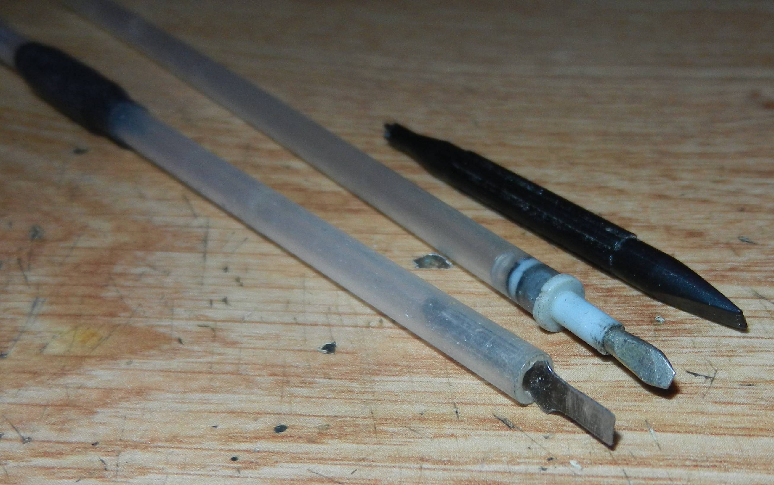
Image 34: Overview photograph
Adjust this new replaced R1’ resistor network according to table for your specific frequency.
Now install PCBA into powered off Fluke 510A, turn it on and check oscillations with oscilloscope and frequency counter. Frequency should be close to desired nominal value. Sinewave should look clean without blur or distortion and stable in amplitude. If waveform looks distorted or unstable or incorrect frequency go back to previous steps and correct the mistakes. Do NOT adjust any trimmers or settings inside the unit, only test frequency setting PCBA.
If all works correctly, let 510A to warm-up some time (10-30 minutes will be good duration) and connect voltmeter to test point TP5. Adjust trimpot resistor R1’ to meet gate voltage within -2.5 VDC ±0.2 VDC. This adjustment is very important for output frequency. If front-panel port adjustment does not allow desired frequency setting, you’ll have to fine-tune and adjust capacitors C1’ and C2’, after which perform R1’ adjustment steps again. After doing this multiple times you should get good stable signal and desired frequency. After final adjustment reassemble Fluke 510A and let it settle overnight before doing the final measurements and tests.
Resistors used for R1’ trimmed network should be 1% or better with decent temperature stability. Measure original R1’ resistor before desoldering it, in-circuit, otherwise you might get incorrect measurements due to thermal stress from soldering and heating.
These adjustment steps should be performed for each frequency board inside the target 510A unit it supposed to be installed in. Prepare some ESD-safe boxes or bags to store unused frequency boards, so they are not affected by mechanical or physical stress in storage.
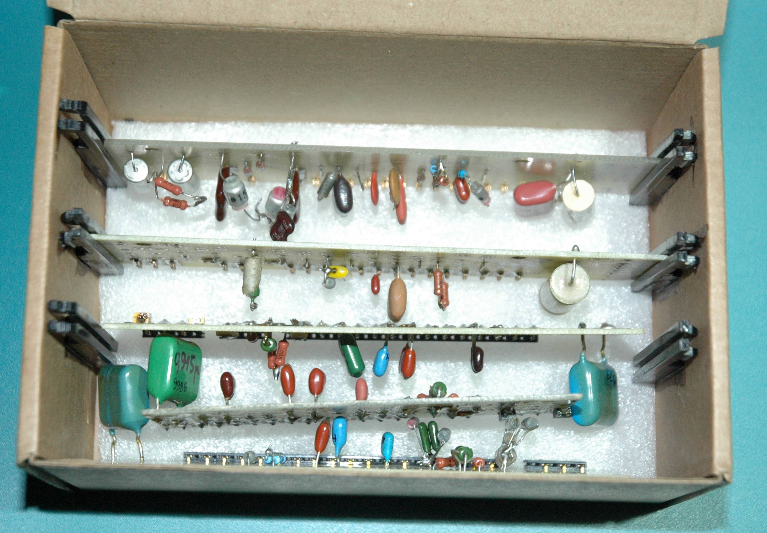
Image 35: Storage container for frequency boards

Image 35: Empty container with slot guides for PCBAs
Ensure there is no dust or corrosion in connectors.
Safety precautions
After both of my Fluke 510As gave me juicy shocks from their live 230V exposed mains this note was added here. It was shocking to see in Fluke device, but connection of mains wiring to power switch are not covered by plastic isolators/tubes, as shown on photo below.

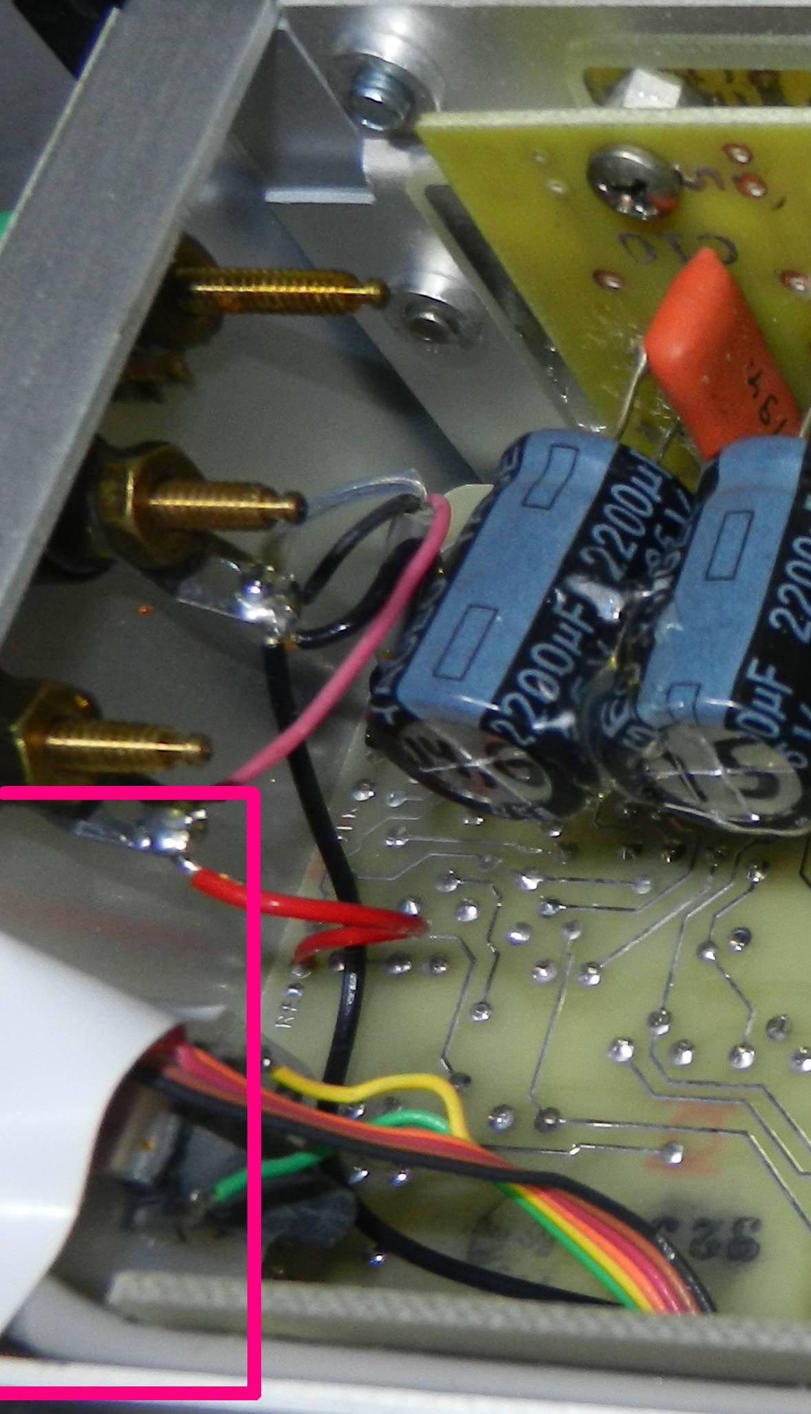
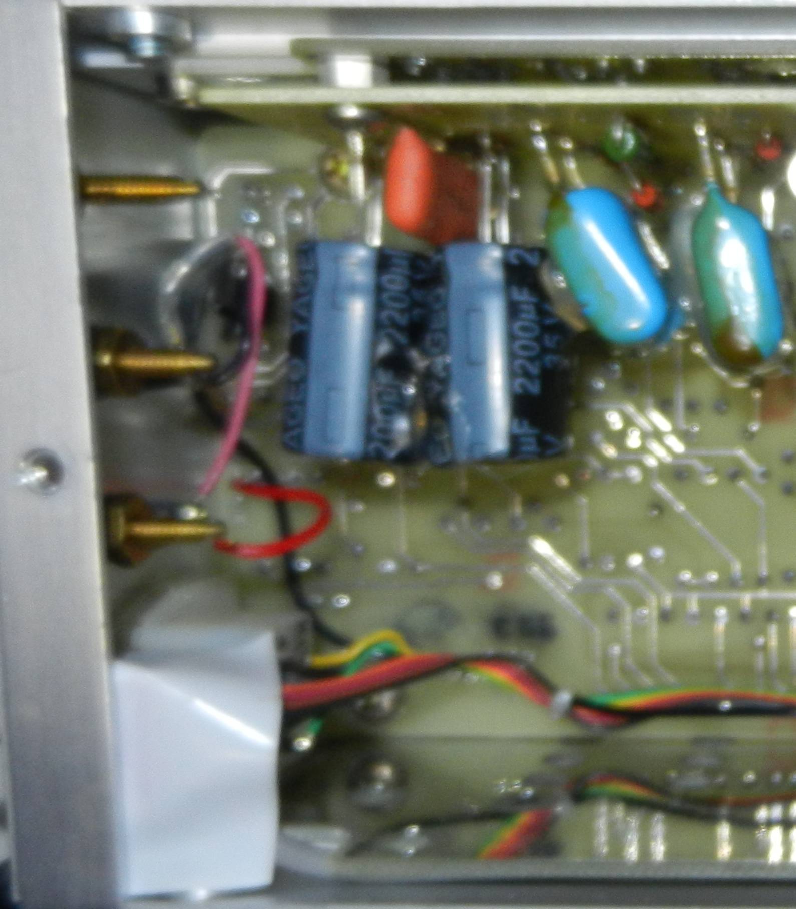
Image 36-38: Taped mains connector to reduce risk of electric shocks
Simple solution – add few tape pieces on top of the exposed metal. Excuse the crudeness of setup, but health safety is more important here.
Measurement results with Fluke 510A
Output temperature coefficient for the reference voltage was measured about -5 ppm/°C.

Image 39: Measured temperature coefficient of Fluke 510A’s internal voltage reference
Output voltage with 1 kHz signal show thermal stability same -5 ppm/°C on one of my HP34401A (here and later will be called “old DMM”). Newer DMM shows less than -2 ppm/°C (Image 41).
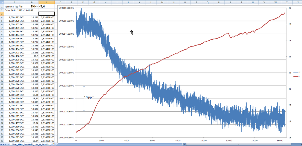
Image 40: Temperature stability measurement with older 34401A DMM

Image 41: Temperature stability measurement with newer 34401A DMM
With other frequency bands it much worse. Maybe my HP/Agilent 34401A’s are to blame here as they were never adjusted or calibrated for AC Voltage functionality with traceable metrology standards.
Frequency 10 kHz: -13 ppm/°C ppm/°C with old DMM

Image 42: Test of temperature stability with 10kHz output

Image 43: Test of temperature stability with 62kHz output
High frequency -60 ppm/°C for 62 kHz with older DMM (it cannot do higher frequency due to repairs in AC circuitry. I used different opamps due to lack of original components source) on Image 43.

Image 44: Test of temperature stability with 100kHz output on newer HP34401A
New DMM show result +150 ppm/°C for 100 kHz frequency.
It’s bit tricky to interpret results of these measurements, especially on higher frequency signals. One meter shows negative temperature coefficient, newer shows possible, so which one telling lies?
But it’s not matters much, because actually both results are well within specifications of the HP/Agilent 34401А DMM. We will look into more details on part 3 article later.
THD measurements performed on this Fluke 510A with frequency boards were also summarized in Table below.
| THD | F510A | Frequency | 10 Hz, dBm | >0< | % | 1 kHz, dBm | >0< | % | 100 kHz, dBm | >0< | % |
|---|---|---|---|---|---|---|---|---|---|---|---|
| Fundamental | 1 | 8.19 | 0 | 7.69 | 0 | 7.44 | 0 | ||||
| 2 | -69.07 | -77.26 | 0.01371 | -74.25 | -81.94 | 0.007998 | -68.88 | -76.32 | 0.015276 | ||
| 3 | -73.25 | -81.44 | 0.00847 | -74.43 | -82.12 | 0.007834 | -77.78 | -85.22 | 0.005483 | ||
| 4 | -82.37 | -90.56 | 0.00296 | -101.25 | -108.94 | 0.000357 | -75.75 | -83.19 | 0.006926 | ||
| 5 | -85.86 | -94.05 | 0.00198 | -77.87 | -85.31 | 0.005426 | |||||
| 6 | 0 | -81.69 | -89.13 | 0.003495 | |||||||
| 7 | 0 | -85.94 | -93.38 | 0.002143 | |||||||
| 8 | 0 | -98.18 | -105.62 | 0.000524 | |||||||
| 50 Hz | -86.28 | -94.47 | 0.00189 | ||||||||
| Total | 0.0164% | 0.0112 % | 0.0189% | ||||||||
THD was measured by HP3588A spectrum analyzer from a friend during weekend in home lab environment. There was no faraday cage shielded room, plenty Wi-Fi and SMPS-powered devices around, air drafts and so on. THD measurement setup and more detailed results will be shown in future articles.
Summary
I’m quite satisfied with Fluke 510A and this entry to AC performance adjustments and experiments. There is always desire for better, for example 3 frequency output at the same time. And also with lower attenuated voltages. And I have this already in works, more details coming in following articles in this series.
Also DIY frequency boards for Fluke 510A worked well, at least same as original Fluke units.
Discussion is very welcome thru comment section or at our own IRC chat server: irc.xdevs.com (standard port 6667, channel: #xDevs.com). Web-interface for access mirrored on this page.
10.04.2020. TEKTRON
Modified: Dec. 22, 2020, 8:12 p.m.