Choosing thermometer for temperatures below zero °C is not always a simple task, specially if you are hobbyist, which also often imply lack of extra funds. Advanced and precise reference meters cost in such cases is usually prohibitive, most of industrial meters often have lack of temperature range, cheap devices for less that $50 USD have mediocre accuracy for subzero temperatures. Good meters more affordable on secondary market, such as Fluke 51, 52 and newer 51 II and 52 II meters, being for sell at $100-150 USD range on eBay and such.
In this article we will take a look on Fluke 51-II and try some ideas how to improve it by modification to get more expensive model with more features for free. :D User manual for meter is available here
Feature comparison
Before we go any further, short feature reminder and modern Fluke 50 II series thermometers specs:
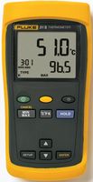
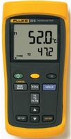
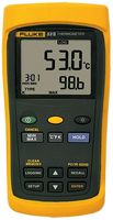
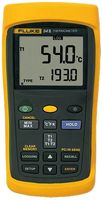
| 51 II features | 52 II features | 53 II features | 54 II features | |
 |
 |
 |
 |
|
| Amount of channels | 1 | 2 | 1 | 2 |
| Range | -250°C to +1372°C (depends on TC type) | |||
| Accuracy | +- .05% of reading + 0.3°C for Type K. | |||
| Power | 3 x AA batteries | |||
| Display | LCD with green (ugly) backlight | |||
| Thermocouple type | K,T,J,E | K,T,J,E | K,T,J,E,R,S,N | K,T,J,E,R,S,N |
| Time stamp feature | No | No | (Relative time) | |
| Ratiometric mode | No | T1-T2 diff mode | No | T1-T2 diff mode |
| Datalogging | No | No | Up to 500 measurements | |
| Software support | No | No | FlukeView Software (cost extra) | |
| Interface | No | No | Infrared | |
They look similar, sharing same chassis, LCD and controls. and likely using exact same PCB inside. Photo of full featured 54 II PCB would let us know if this expectation true and then we can try some hacking our 51 II to become same hardware-wise. There is big hope that firmware in meter’s brains is universal for all models.
Most of reverse engineering actually was done first hour after I received meter, but later … Let me tell full story here.
Internal construction
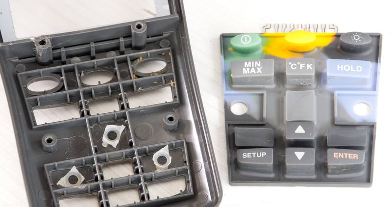
Soldering stuff and wrecking hardware is often most favorite thing engineers do. So is disassembling gear. Let’s take a look inside Fluke 51 II (MSRP ~$220 USD).

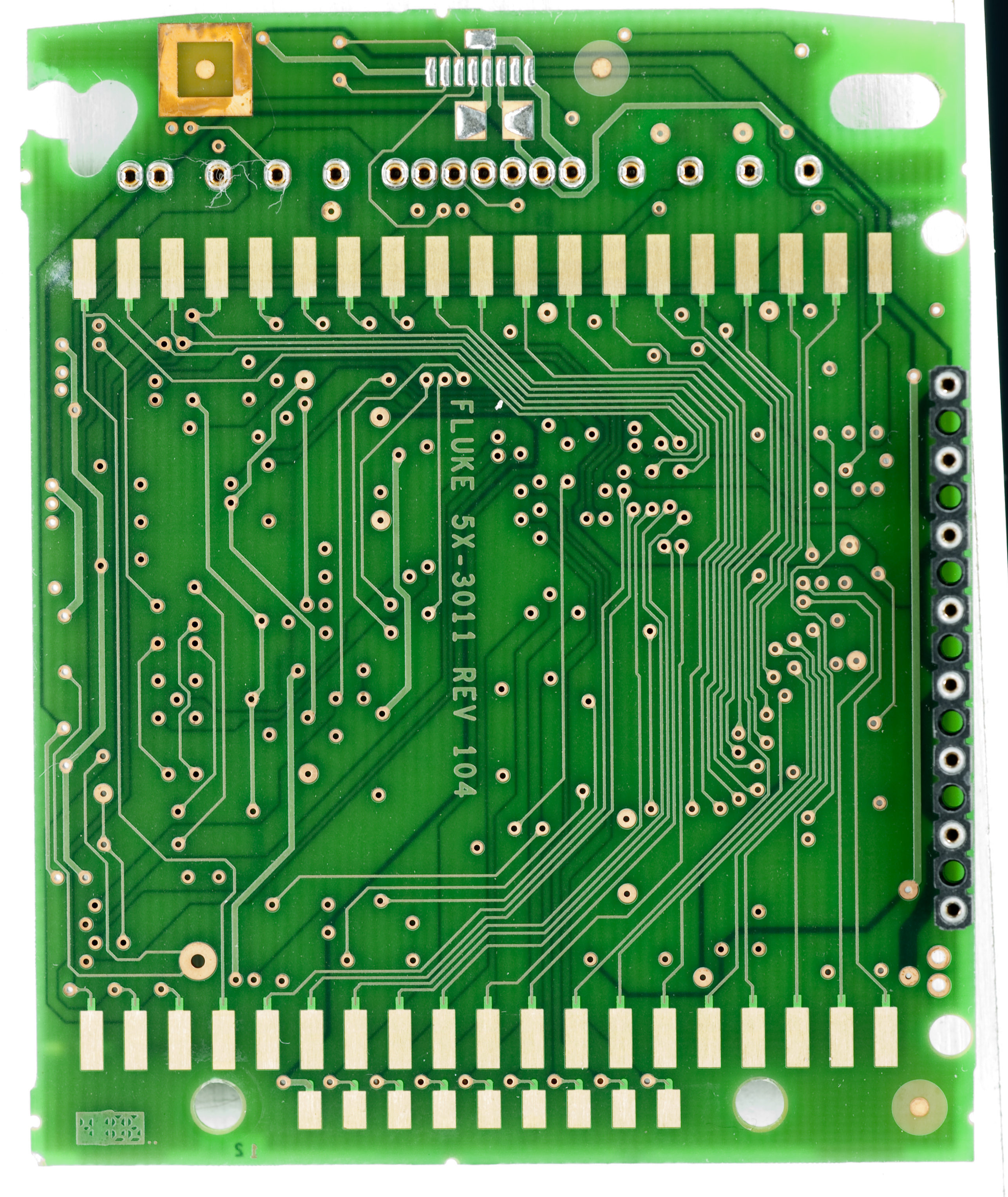
As we now see, it’s Fluke 50 II series PCB, marked 5X, exactly same for all four meter SKUs, 51, 52 , 53 and 54.
It’s quickly becoming obvious that everything inside, including keyboard and main PCB is EXACTLY same as in most advanced 54 II (MSRP $370 USD) version.
Fluke engineers designed fully featured model and then make lower-priced models by limiting features and not soldering extra parts on PCB, such as second thermocouple channel, IRDA interface, memory for data-log function. It is very common practice, as it’s much easier to remove functions/hardware just by BOM or firmware update, rather than supporting multiple hardware versions with own production flow and design support.
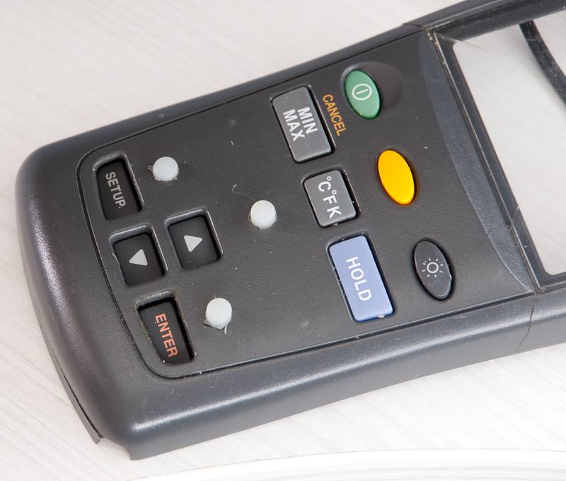
Smart move, I like hardware design to be implemented this way. People who have too much extra time don’t care loosing warranty can bring full features back rather easily. Only the enclosure of meter is different (51 II have missing two extra holes in plastic for second thermocouple and lacks of three buttons (two for logging features and one T1-T2 switch). Buttons tops in rubber membrane are cut, but still can function if mill proper opening in plastic chassis and use spacers, which close contacts on film keyboard on push.
Things could go bad if Fluke flashed unique firmware, limiting features in cheaper meters, because there is no way to get secured firmware from modern meter’s MCU. So I tried everything on my own risk, to see what happen. Let’s start here with few high-resolution pics of 51 II PCB.
Fluke’s service manual is rather useless for internals analysis, as it does not contain any component level information, leave alone stuff like schematics or BOM list.
Lets dig into details and components found onboard. Big chip in center – Texas instruments MCU ASIC. I was lucky enough to get REV 101 meter version, likely early board, where original TI marking was present. This is 16bit MSP430P337I chip, with one-time-programmable firmware from Fluke. Later meters have same MCU but with Fluke markings only. Most of Fluke portable tools are using TI chips, so no wonder here. Used chip have 16-bit cpu core, UART and SPI links, hardware 16×16 multiplier and LCD controller.
Looking at board counterclockwise from the left we found generic amplifier LMV321M5 in SOT23-5 for LED back-light current source. Then power supply – two National LP2980 LDOs (precision 0.5%, 50mA output current , output voltage +2.8 VDC), then DC-DC using switching capacitor tech Linear LT1044, and 12.5MHz oscillator for CPU.
Heart of meter analog frontend is sigma-delta ADC Linear LTC2400, with awesome 24-bit resolution, 4ppm tol and 0.5ppm bias with 110db SNR. Maximum conversion speed – 6 Hz. Cost of just this chip, without anything else – approx $8 USD on small amounts from Linear shop. Near it we can opamp Linear LT1097 – low-noise high precision amplifier with 50µV offset, temperature drift 1µC per °C, CMRR 115dB, used as thermocouple voltage amplifier. Next three big chips – analog muxes, dual 4:1. I’m using similar 4051 in my Neutron power supply tester and other projects, so familiar with them. 8-leg chip near them is TI TLC3702C – comparator, looks like used for detection of open sensor input.
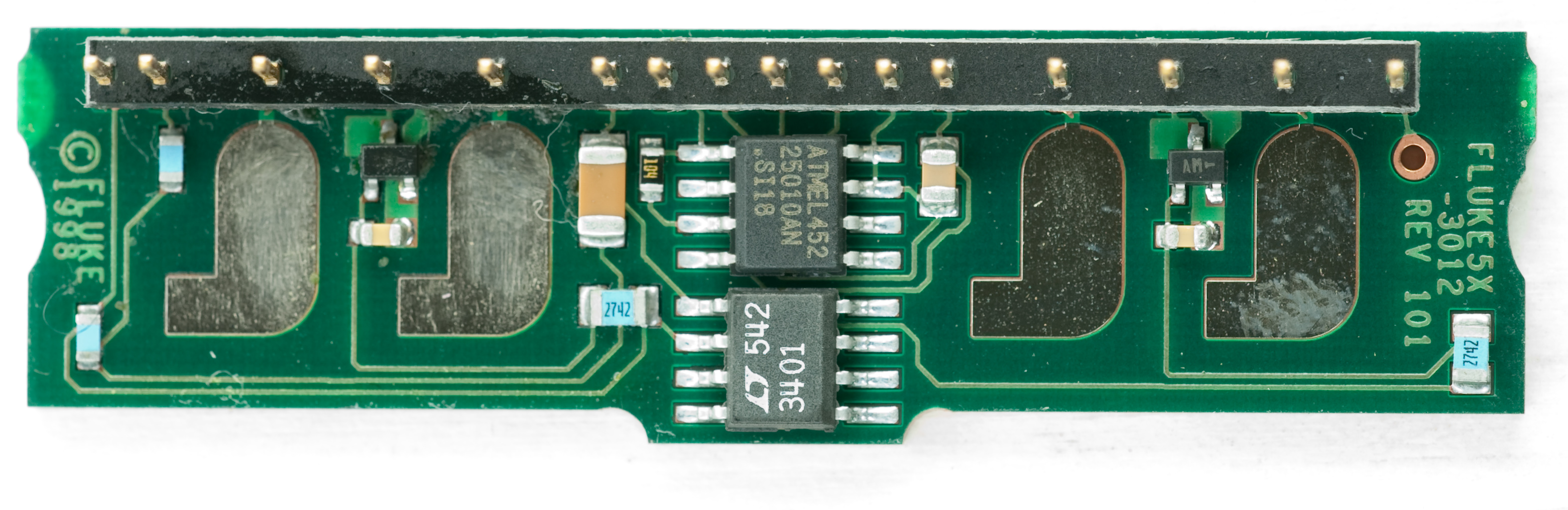
Thermocouple contacts are connected by separate springs to gold-covered pads on special board, placed to collet pins into mainboard. All contacts are covered with gold, oxidization shall not pass. For precise temperature measurement it’s also very essential to have constant and known temperature of cold junction, where thermocouple input connected to meter.
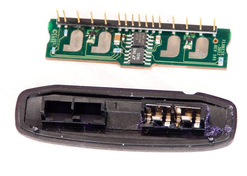
Connector board made from 1.3mm thick pure copper substrate with thin insulation layer and parts on single side over it. This amount of copper mass maintain temperature of all contacts very close and stable. Such board manufacturing is rather expensive, more expensive than generic 4-6 layer board, as an for example. Nice attention to construction from Fluke, no doubt.
Component side of this copper pcb also have two ICs, one of which is simple ATMEL AT25010AN – this is 1 Kbyte memory where calibration data stored. And near it LT1034CS8-2.5 voltage reference from Linear Technology, according to marking (3402).
Model ID hacking
Recall to back PCB shot – we have meter mode straps. These are resistors R50, R49, R51 and R52.
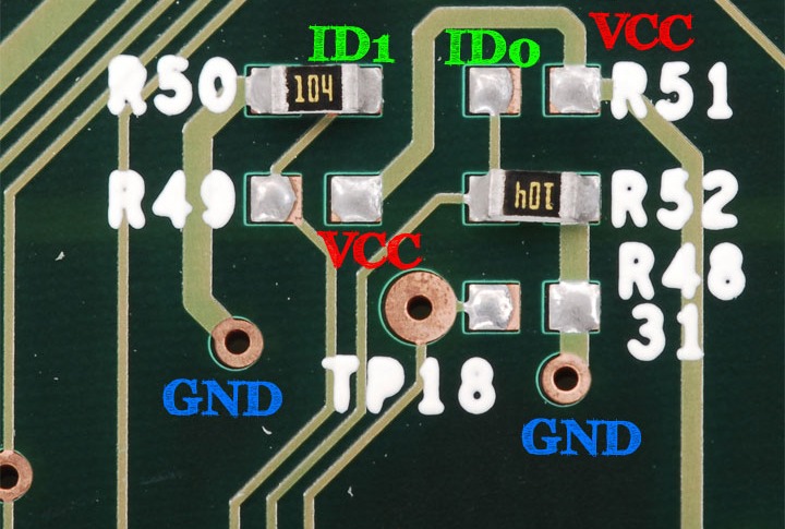
This is common approach to implement configuration of firmware mode, reading hardware level on resistive divider, and used widely in digital electronics, including PC graphic cards, motherboards, processors, you name it. Readers who often visit this site may already remember seeing straps on memory option upgrade article for Keithley Instruments DMMs.
General concept and operation is simple – usage of soldered resistors as fixed switch, connecting either +3.3V or ground to digital input, which can be read as one or zero from firmware code.
For this to work, put two resistor footprints on PCB, each with one pad (usually middle) tied to one input pin of CPU/GPU/controller etc. Other pad of one resistor tied to ground, secondresistor – to VCC power or I/O level power. If we solder resistor to ground signal – then input to chip will be zero, meaning logical zero visible to firmware.If resistor to power pad populated, then we have power high level connected to digital input, thus translating to logical one in firmware.
Such pairs always have only ONE resistor at time, because soldering two resistors for same digital line to both will get us undefined condition with middle voltage level signal. This is wrong, from digital input logic perspective, and can be read one or zero, depending on input type.
I’ve spotted these resistors and get clear idea what is it, with having clear powers and grounds with two inputs.
Yes, it’s 2-bit code present here, as only four resistor locations present.
Actual value of resistors is not that important, in this case it’s 100 kΩ resistor – just to minimize current flow thru pin, because our meter is battery powered and this is critical to have as small power consumption as possible for these resistor networks. As we know from Ohm’s law, less resistance – more current flow. With more resistance – input pin could be less immune to noise and get wrong state by accident, but even few microamps for modern microcontrollers are enough to have reliable detection. I resoldered resistors to another footprints and doing so few times quickly figured out all possible modes.
Table of states:
| ID[1:0] | Firmware mode |
| 00 | Fluke 51 II mode |
| 01 | Fluke 52 II mode |
| 10 | Fluke 53 II mode |
| 11 | Fluke 54 II mode |
First success: firmware code is same across all models, and operation mode just selected on manufacturing phase, by soldering resistors on proper place. Cool! Without this step any further hardware hacking would be extremely compromised.
Conversion of Model ID from 51 II to 54 II is now done by changing this simple resistor configuration change. It detected as full-featured 54 II model, two inputs with all extra stuff in menu present as 54 II. But there was missing some passives on PCB, so second channels was not operable yet. It just told -0L, meaning overrange. We will get back to fixing second channel in next chapter.
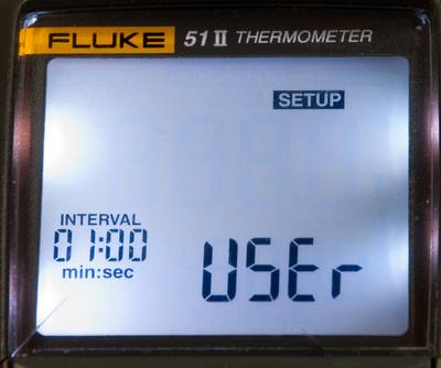
Every feature from 54 II like on photo below.
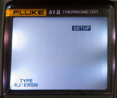
Thermocouple Types – all present here, KJTERSN (original 51 II and 52 II have only KJTE)
Interval feature for datalogging absent in original 51 II and 52 II meters now in menu:
Modify hardware to add second thermocouple channel
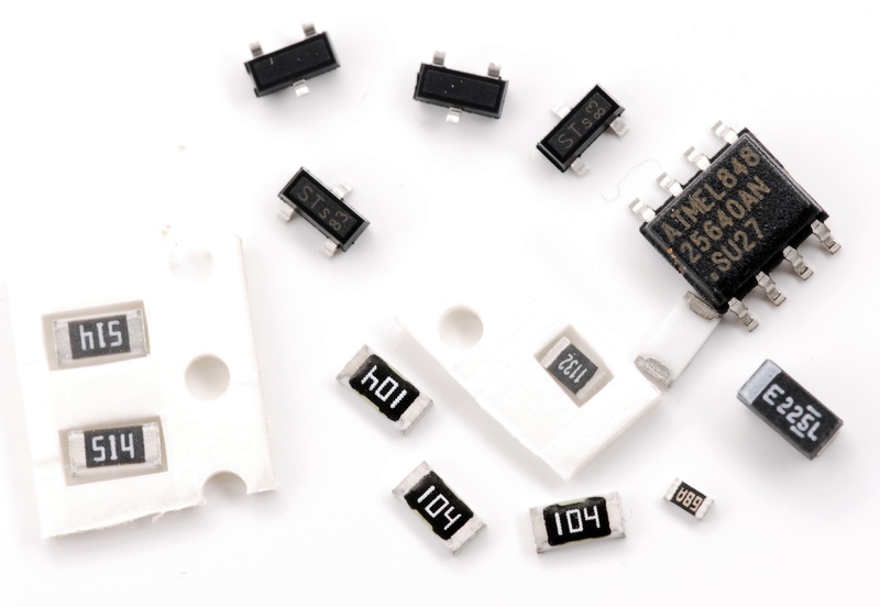
Time to add second channel now. Knowing already that Q1, Q3, Q2 and Q4 on top was MOSFETs in SOT-89 package I found datasheet on original DN2540. These are depletion mode JFETs, in contra to wide-used enhanched mode MOSFETs found everywhere on motherboards and graphics card. Difference was that these FETs closed with negative gate voltage, not zero. I reverse engineered schematic of this part:
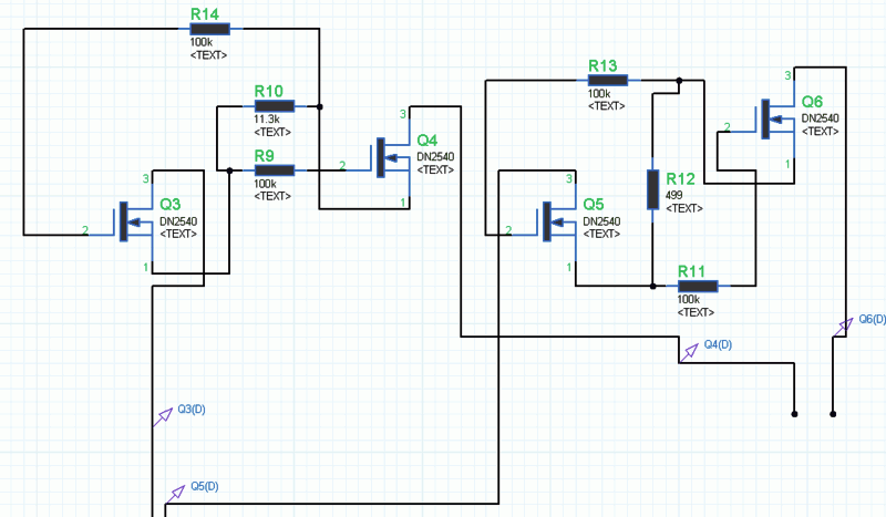
Simulated it with SPICE modeling, got nothing but voltage switch/follower here. Correct me if I’m wrong :)
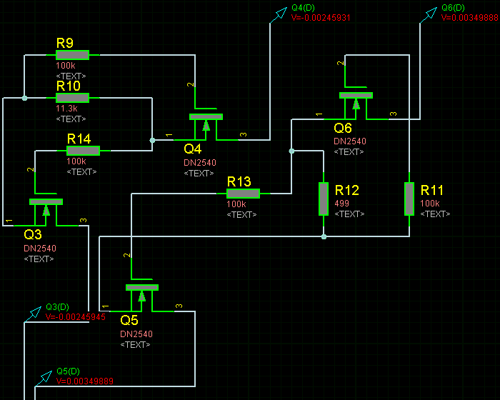
Looks like they used for muxing here, to isolate channels when they are not needed, to avoid errors in readouts and signal measurements. I did not found original JFETs source at time of modification, so decided to go with generic depletion-mode JFETs in smaller SOT-23-3 package. Ones I used are BSS139. Back to soldering now.
To solder SOT23-3 on SOT-89 pattern used piece of wire to connect dummy collector pad to central pad. After 10 min and some aid of microscope, homework was completed.
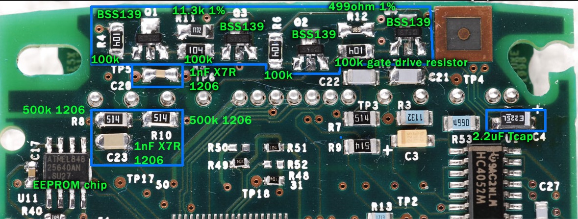
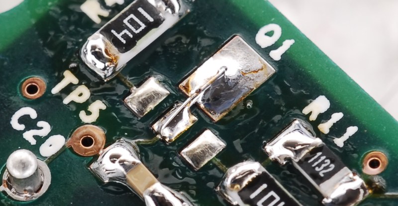
Notice C4 cap on right – it’s tantalum capacitor, beware right polarity (marked line is positive here). 2.2 µF 6V or similar will fit nicely, using SMA package. R8 and R10 are just similar as R7 and R9, 500 kΩ 1206 resistors with 5% tol. R4, R5, R6 and R17 are gate resistors, all 100 kΩ 1206 with 5% tol. R11 and R12 are 1% resistors for thermocouple input signal, 11.3 kΩ and 499 Ω.
Take care to use best tolerance and low tempco resistors, if possible. And important part here are capacitors C23 and C20. These highly affect precision and channel “crosstalk”, during testing best results were archieved with 1nF 0805 and 1206 5% capacitors. I could not find NP0 capacitors on hand, so used X7R, but would recommend using C0G or NP0, as it should be.
Original Fluke design (C22 C21 eg.) using NP0-type caps. NP0 dielectric type have zero temperature drift and much more precise as in term of capacity to X7R type. NP0’s usually much more grayish and ligher color in appearence, and have much lower maximum capacitance in same package.
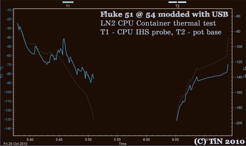
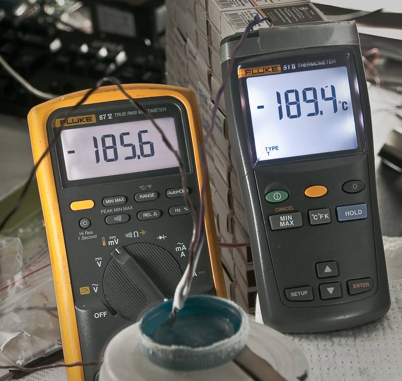
These modifications to board now allowed using second channel, and now we getting correct temperature readout.
Later I tried just shoring drain and source pads on Q1, Q2 Q3 and Q4 patterns, without soldering gate resistors and transistors – second channel worked this way too, but doing so is at your risk!
LCD Backlight modification
Also changed backlight from green to white and adjusted current source for more current for leds, so now it looks much much better than original ugly green dark BL. Four white color SMD-leds with size 1206 was soldered on wires with teflon insulation placed to side of plastic lightspreader on back LCD. I don’t care much about battery life, so adjusted brightness of leds but raising current a bit. This was done by adjust to feedback of amplifier LMV321M5 (chip U9) by soldering R26 from 10k to 4.7k to feed more current to leds.
Simple as it is, but much better usability now, can use meter in the dark without any problems. Stock dark-green backlight is really bad on these Fluke’s.
Datalogging
I drilled plastic case of meter and instert round rubber spacers for extra keys, as you see on photo. Need better rubber blocks to make “native-look” buttons
Not as neat, but it works!
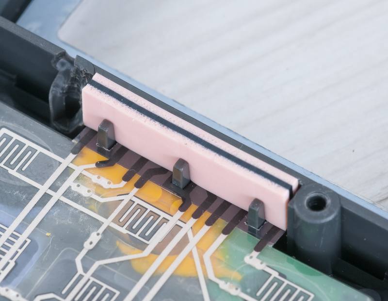
Rubber connector between membrane keypad and PCB is rather sensitive, so take care to keep it clean and firmly fixed.
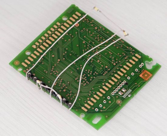
To test interface I used serial programm on PC and connected meter’s RX/TX lines to UART-USB Serial converter (Silicon Labs CP2103). Result is expected:
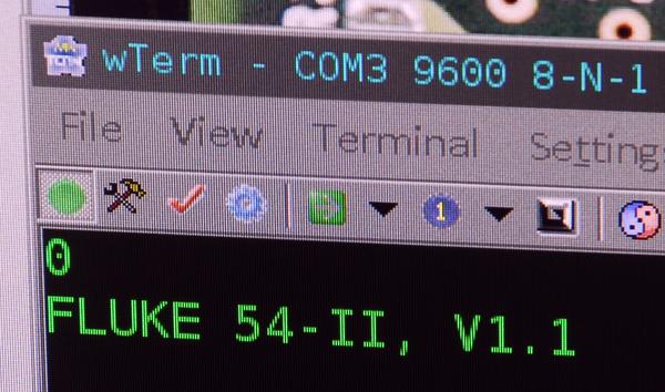
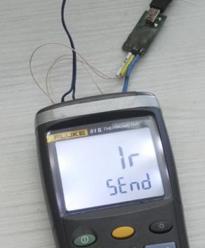
Terminal software from USB-UART bridge chip between Fluke got correct data with 9600 8N1 port settings.
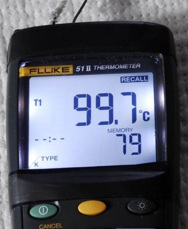
Testing datalogging complete!
Summary
So total list of parts used for modification this Fluke 51-II meter into $150-more 54-II:
- ATMEL AT25640AN SPI EEPROM
- Three 100 kΩ SMD resistors
- Two 510 kΩ SMD resistors
- One 11.3 kΩ SMD resistor
- One 499 Ω SMD resistor
- Four of BSS138 JFETs
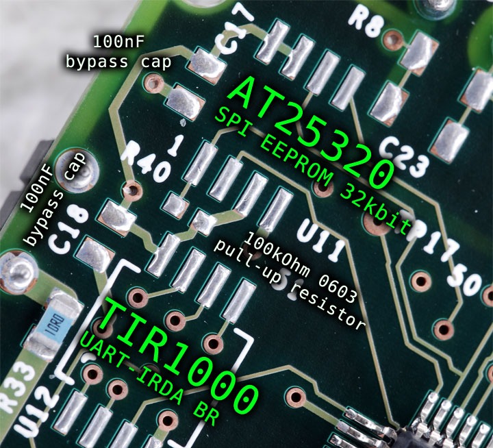
If you want use IRDA function to transfer data to PC, you can add TIR1000 chip, or just route three wires to your favourite UART-USB Serial dongle, like I did:

Jump into comments if you interested in this or have any suggestions.
Modified: Nov. 25, 2015, 8:02 a.m.