Contents
- Intro
- Disclaimer
- Project goal
- Reference circuit
- Temperature control circuit
- Schematic design
- Layout design
- Assembly notes
- Considerations while building and using ultra-precision references
- Initial data results
- Thermal analysis
- Test chamber design
- Temperature coefficient measurements and analysis
- LM399 low-cost version
- Layout design of low-cost version
- Performance verification
Intro
There is increasing demand of better stability, lower noise and higher accuracy for voltage reference sources in modern high-precision instrumentation. The best voltage standard is using the Josephson effect. Josephson Junction Array (“JJA”) modules are used today in metrology institutions and calibration labs to provide definition of SI volt unit. It’s known that the JJA output voltage is predicated on a cryogenic physics constant, which results relative voltage uncertainty of less than 1*10 -10 /year. But using JJA in lot of applications is prohibitive, due to fact that it require liquid helium to operate at temperature of few K. There are not many labs are able to maintain high operation cost of JJA, to keep as primary reference. For reference, complete PJVS (Programmable Josephson Voltage Standard) system from NIST is available for $306K, with JJA chip cost $50200 USD.
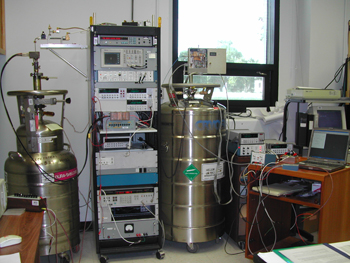
Photo courtesy: NIST PML
Linear Technology LTZ1000 Ultra-Precision Reference
The LTZ1000 is an ultra-stable voltage ovenized zener reference manufactured by Linear Technology. It has two major components that make it the one of most stable commercial reference available[3]. The first is a buried zener junction, which provides the reference voltage, and the second is a temperature sensing heater, which maintain substrate temperature constant. Its superior precision comes at the cost of substantial and expensive (due to requirement of very high stability resistors) external circuitry that must be used to set its operating currents and bias voltages.
Disclaimer
Redistribution and use of this article or any images or files referenced in it, in source and binary forms, with or without modification, are permitted provided that the following conditions are met:
- Redistribution of article must retain the above copyright notice, this list of conditions, link to this page (/article/kx-ref/) and the following disclaimer.
- Redistribution of files in binary form must reproduce the above copyright notice, this list of conditions, link to this page (/article/kx-ref/), and the following disclaimer in the documentation and/or other materials provided with the distribution, for example Readme file.
All information posted here is hosted just for education purposes and provided AS IS. In no event shall the author, xDevs.com site, or any other 3rd party, be liable for any special, direct, indirect, or consequential damages or any damages whatsoever resulting from loss of use, data or profits, whether in an action of contract, negligence or other tortuous action, arising out of or in connection with the use or performance of information published here.
Project goal and specifications
- Maximum stability for DC voltage reference
- Ultralow tempco Vishay Z-foil resistors to minimize tempco
- Linear LTZ1000 ultrazener [4]
- Digital thermal sensors for external calibration purpose
- Wide range input supply voltage
- Compact form factor
- 1ppm/year voltage output
- 7.15VDC ±1% direct output
- Thermostat setpoint +65°C
- Kelvin sense output
- Single-rail voltage input
- 2.54mm SIP connection ports
- Optional temp sensor for LTZ can
| Item | Value | Units |
|---|---|---|
| Input voltage Vin, reference module | +24.0 | VDC |
| Input voltage Vm, monitoring section | +6.0 | VDC |
| Output current, Reference output at VREF port | 1 | mADC |
| Output current, Temperature output at TM port | 20 | mADC |
| Operating temperature range | 0 to +50 | °C |
| Storage temperature range | 0 to +80 | °C |
| Lead temperature (soldering, 10s) | +240 | °C |
Table 2: Absolute maximum ratings and specification for assembled module
This development module is intended for laboratory development and engineering use only. It is NOT a final product for mass production.
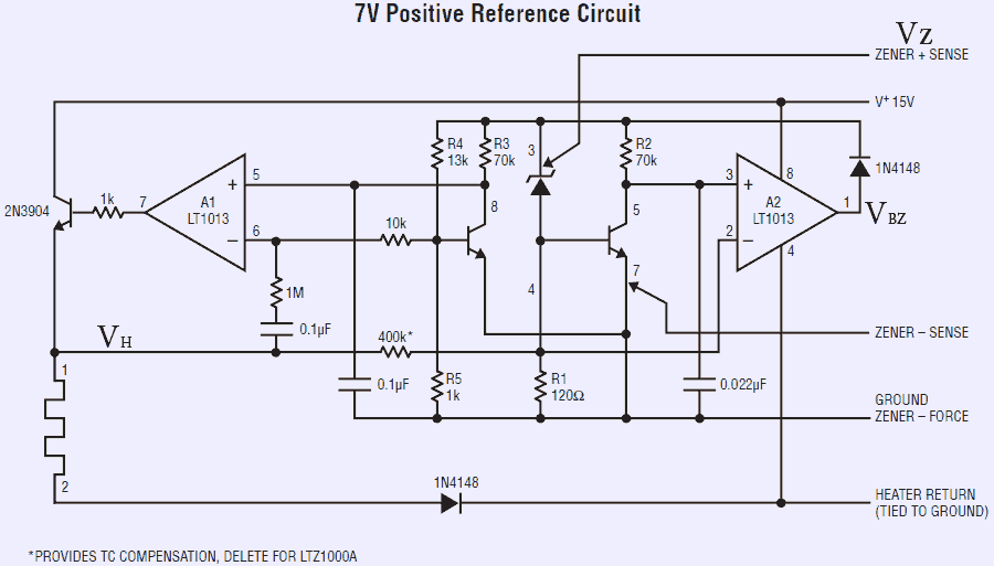
Reference circuit
The reference circuit consists of a buried Zener diode junction and a temperature-compensating “sensor” transistor (both of which are built into the same LTZ1000’s die package). External resistors, a filtering capacitor, and an operational amplifier are used to provide bias and compensation signal. Because zener is buried below the surface of the silicon (hence the name, “buried”), this precision zener is able to reduce oxidation and contamination problems during manufacturing. These issues make regular Zener diodes practically useless as precision references. The reference circuit section schematic is shown below.
During power-up, the op-amp tries to set the base-collector voltage of the transistor to zero. In doing so, it source current to reverse bias the Zener diode. Zener acts like a variable resistor in this case, which adjusts its resistance to always drop a voltage VZ of around 6.5VDC. Because of the feedback loop involved, the op-amp sets the transistor collector voltage equal to the Zener anode voltage and in doing so applies a voltage across resistor R2. A small current then flows through R2, such that IC = VZ/R2. For typical R2 at 70 kΩ, the collector current is just around 100 µA. Input impedance of op-amp is very large, rendering almost all of the current to flow through the transistor (with the AC components shorting to ground via the small bypass capacitor), and as it flows through the base-emitter junction, the junction acts like a forward biased diode dropping ~600 mVDC. Resulting overall reference voltage is given by VZ + 600mVDC = 7.1VDC. The voltage across the base-emitter junction is also the voltage across R1, and given it’s resistance, current equals about 5 mADC. This current goes thru the Zener itself, and thus R1 sets the Zener bias current. The reference noise decreases for greater bias currents but the lifetime of the Zener is reduced, as well as long-term drift increases, so 5 mA is a good compromise value. Some of modules use even lower currents for better stability.
Temperature control circuit
The temperature-compensating transistor actually serves a dual purpose in the reference module. By itself, the Zener has a relatively high temperature coefficient of about +2mV/°C, which is clearly unacceptable for precision application. But because the base-emitter junction of the transistor has a temperature coefficient of roughly -2mV/°C, putting the junction and the Zener back to back reduces the total circuit temperature coefficient to almost zero (Naturally a part of the bias current flows into the transistor base but this is negligible because the base current is smaller than the collector current by a factor of hFE, which is around 200 for this transistor. Therefore, the base current is only around 0.5 µA).
Because the temperature coefficients of the transistor and the Zener do not exactly cancel, the LTZ1000 also uses an on-board heater to maintain the substrate at a constant temperature. The heater is powered by a very typical 2N3904 transistor, which is controlled by minute changes in the base-emitter voltage of a temperature-sensing transistor. The schematic for this part of the circuit is shown below.
As before, the transistor collector current is set by R3. R4 and R5 act as a voltage divider and their values are set so that the base-emitter voltage corresponds to the base-emitter voltage at the desired temperature setting. In our case, we use R4 = 13kΩ and R5 = 1 kΩ, so that the base-emitter voltage is around 500 mV. This corresponds to an operating temperature of around +60 °C. Roughly speaking a change of 0.5 kΩ in R4 will change the operating temperature by about 5 °C. In order to maintain a constant temperature, very low tempco precision resistors must be used for R4 and R5.
If the chip heats up above the set temperature, the base-emitter voltage will decrease by 2mV/°C. Accordingly, the collector voltage will also drop, as more current is drawn through R3. This drop will be amplified by the op-amp*, reducing the base current of the power transistor, and hence reducing the power dissipated in the heater.
The complete LTZ1000 circuit puts these two circuits together and is shown below. The positive reference terminal is at +VREF and the negative terminal is at ground. Because the heater is inherently noisy, special care must be taken to make sure that the heater current has its own return path to ground that is separated from the voltage reference ground.
Schematics 1: Linear LTZ1000 reference design schematics (old-rev)
As bonus, here is die photo of my first LTZ1000 chip:

Image 1: LTZ1000A naked die photograph
Schematic design
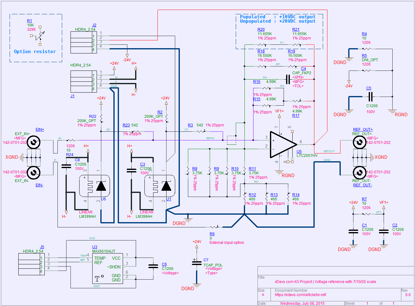
Now, based on everything we learned above, final schematic design for module is shown below:
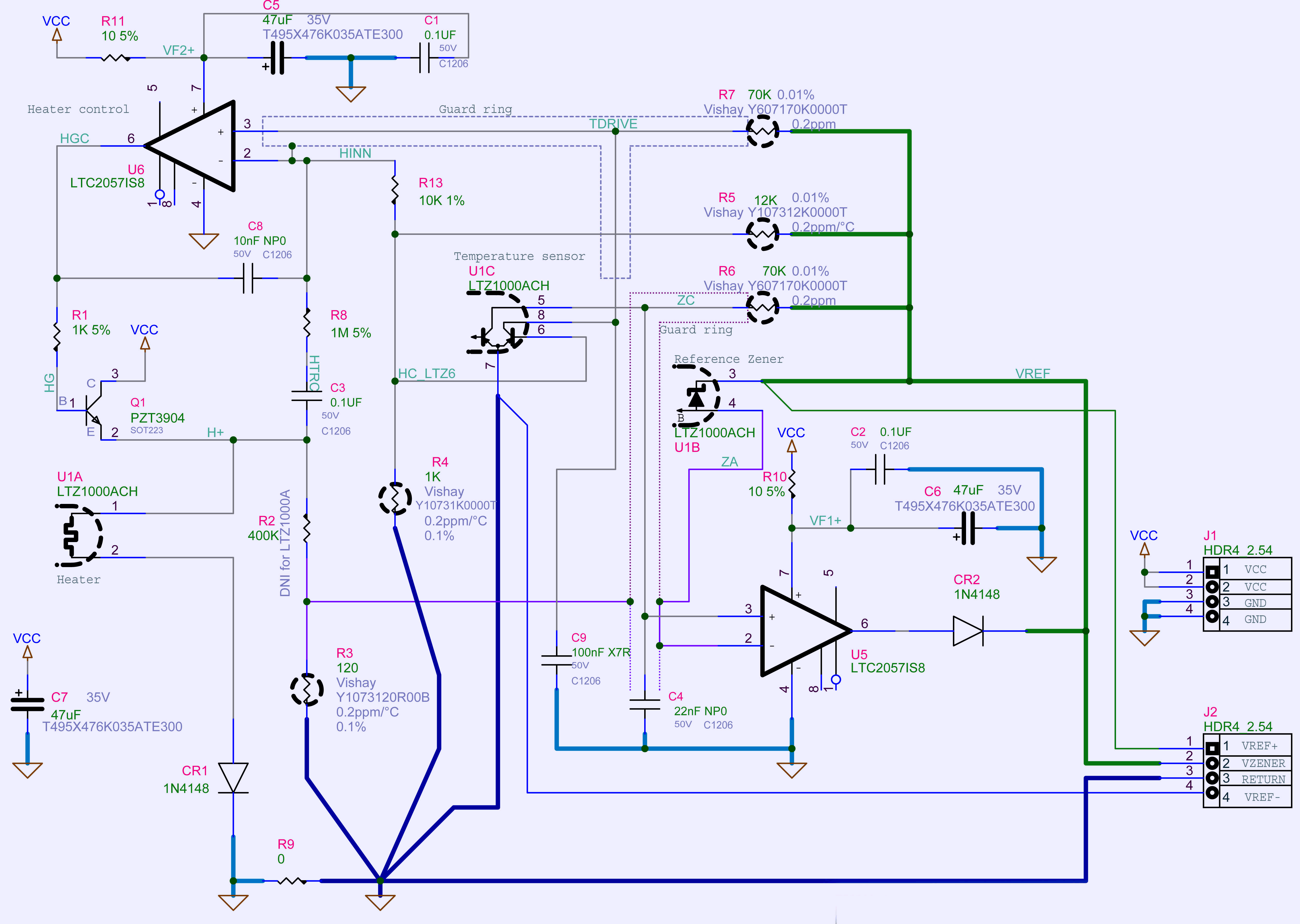
Schematics 2: xDevs.com KX voltage reference (Rev.B00) reference
Auxiliary MAXIM MAX6610 temperature sensors schematic shown below.
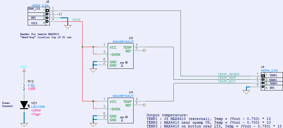
Schematics 3: xDevs.com KX voltage reference (Rev.B00) temperature sense option
Design of this part is straight-forward, following datasheet application for MAXIM MAX6610.
Schematic is available in PDF-format
Schematic and layout design allows installation and experimentation with various industry-standard SO8 single operation amplifiers. Suitable op-amp can be chosen by user, such as:
- Linear LTC2057
- Analog Devices ADA4522-1 in SOIC-8 package
This is not complete list by any means, as almost any op-amp with good performance and supply voltage over +15VDC and ability to use inputs down to 0V will be possible to use for evaluation. I tried few op-amps during initial prototyping and testing, they all worked OK. As result, as due to use in few other ADC/DAC projects of same time period, modern chopper LTC2057 was used. However beware of it’s inherent higher current noise and risk of current spikes coupling. Texas Instruments have this decent application note, explaining the issue in better detail.
If one need guaranteed solution, typical for LTZ1000 reference design bipolar LT1013 is hard to beat, but it’s not compatible with xDevs.com KX board.
Test ports definitions are as shown in tables below
| Board reference | Schematic signal name | Direction,type | Description |
|---|---|---|---|
| J1.1 | VCC | Input, power | Positive power input (+9 to +24VDC) |
| J1.2 | VCC | Input, power | Positive power input (+9 to +24VDC) |
| J1.3 | GND | Input, power | Power return |
| J1.4 | GND | Input, power | Power return |
Table 3: Port definition J1
| Board reference | Schematic signal name | Direction,type | Description |
|---|---|---|---|
| J2.1 | VREF+ | Output, sense | U1 LTZ1000 pin 3 sense output |
| J2.2 | VZENER | Output, drive | Zener reference drive output |
| J2.3 | RETURN | Output, drive | Signal ground return output |
| J2.4 | VREF- | Output, sense | U1 LTZ1000 pin 7 sense output |
Table 4: Port definition J2
| Board reference | Schematic signal name | Direction,type | Description |
|---|---|---|---|
| J4.1 | TEMP_ZENER | Output, analog | External MAX6610 output temperature (connected to J5.1) |
| J4.2 | TEMP_AMP | Output, analog | U3 temperature output (opamp temperature) |
| J4.3 | TEMP_BOT | Output, analog | U4 temperature output (bottom behind LTZ1000) |
| J4.4 | GND | Input, power | Signal ground return |
Table 5: Port definition J4
| Board reference | Schematic signal name | Direction,type | Description |
|---|---|---|---|
| J5.1 | TEMP | Input, signal | Connect to external MAX6610 TEMP pin |
| J5.2 | NC | Reserved | Not connected |
| J5.3 | GND | Input, power | Power return |
| J5.4 | VDC5 | Input, power | +5VDC supply for temperature sensors |
Table 6: Port definition J5
Output temperature can be measured from J4 port and calculated by simple formula : Tsensor = (VOUT – 0.750) * 100
For example if voltage measured from J4.3 was 1.405 VDC, with given formula above we get next result : (1.405 – 0.750) * 100 = 65.5 °C.
This is our measured temperature of chip U4, which is located just under LTZ1000 on bottom side. While it’s not the actual LTZ die temperature, it can help to correlate external temperature impact to actual reference module behavior and drift.
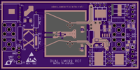
Layout design
Module layout was done using compact size factory-made 4-layer FR4 PCB, with ENIG plating and solder mask.
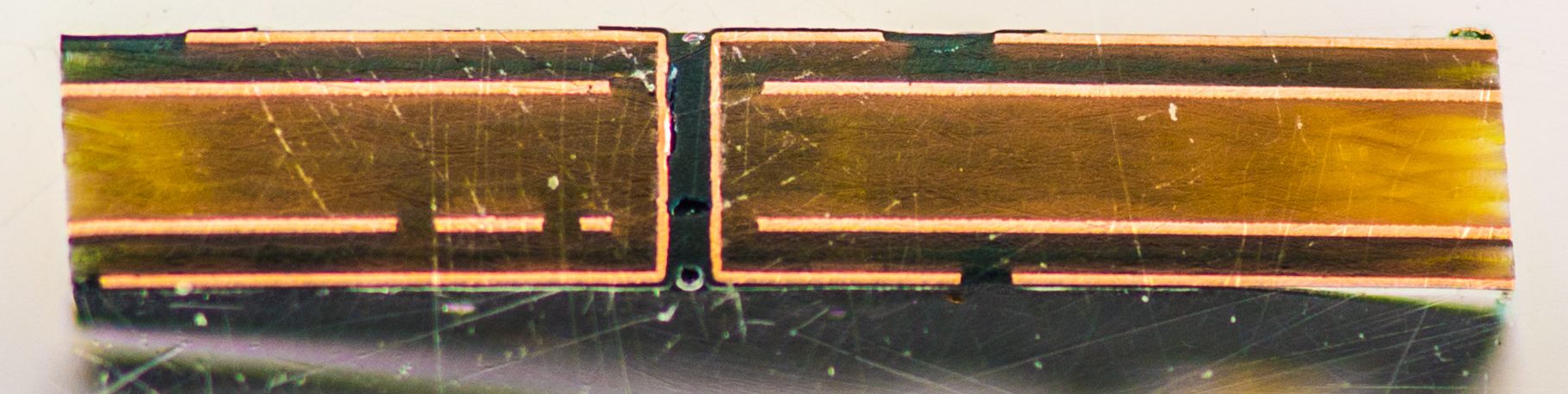
Image 3: xDevs.com KX voltage reference (Rev.B00) PCB cross-section
Inner layers are used for power planes and zener output kelvin connection routing (you can see that by two tiny traces going under top layer).

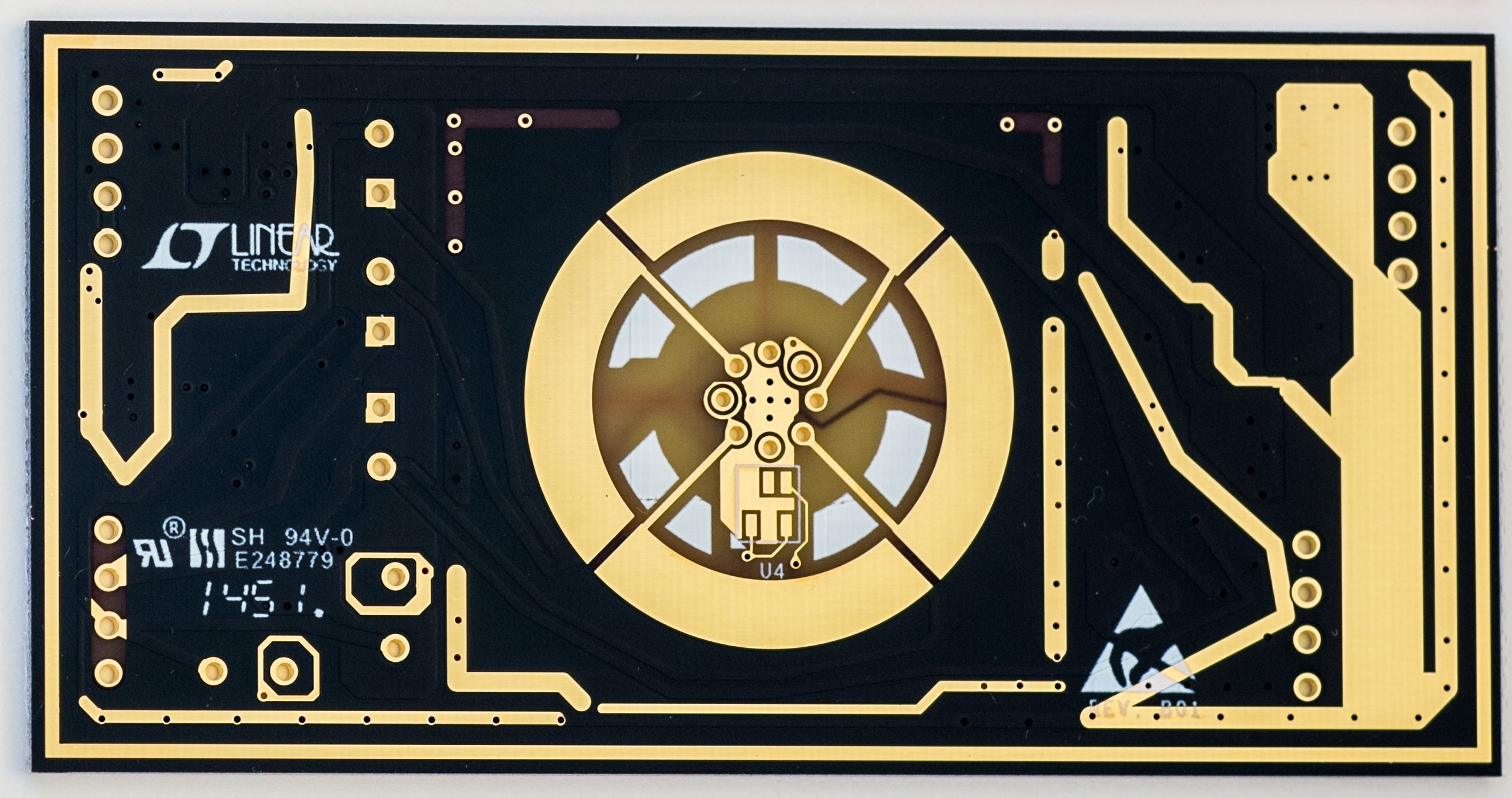
Image 4,5: xDevs.com KX voltage reference (Rev.B00) board, top and bottom side
Idea behind circular copper pads on top and bottom sides around LTZ1000 chip is to keep thermal mass on each side equal, as chip itself will heat PCB under it and even small temperature gradient between pins will degrade reference stability. More detail on this is cover later in this article. Traces going to LTZ pins are made equal length, except kelvin-connected sense pair. Sense for zener’s output is routed on inner layer, directly to J2.1 and J2.4 pins.

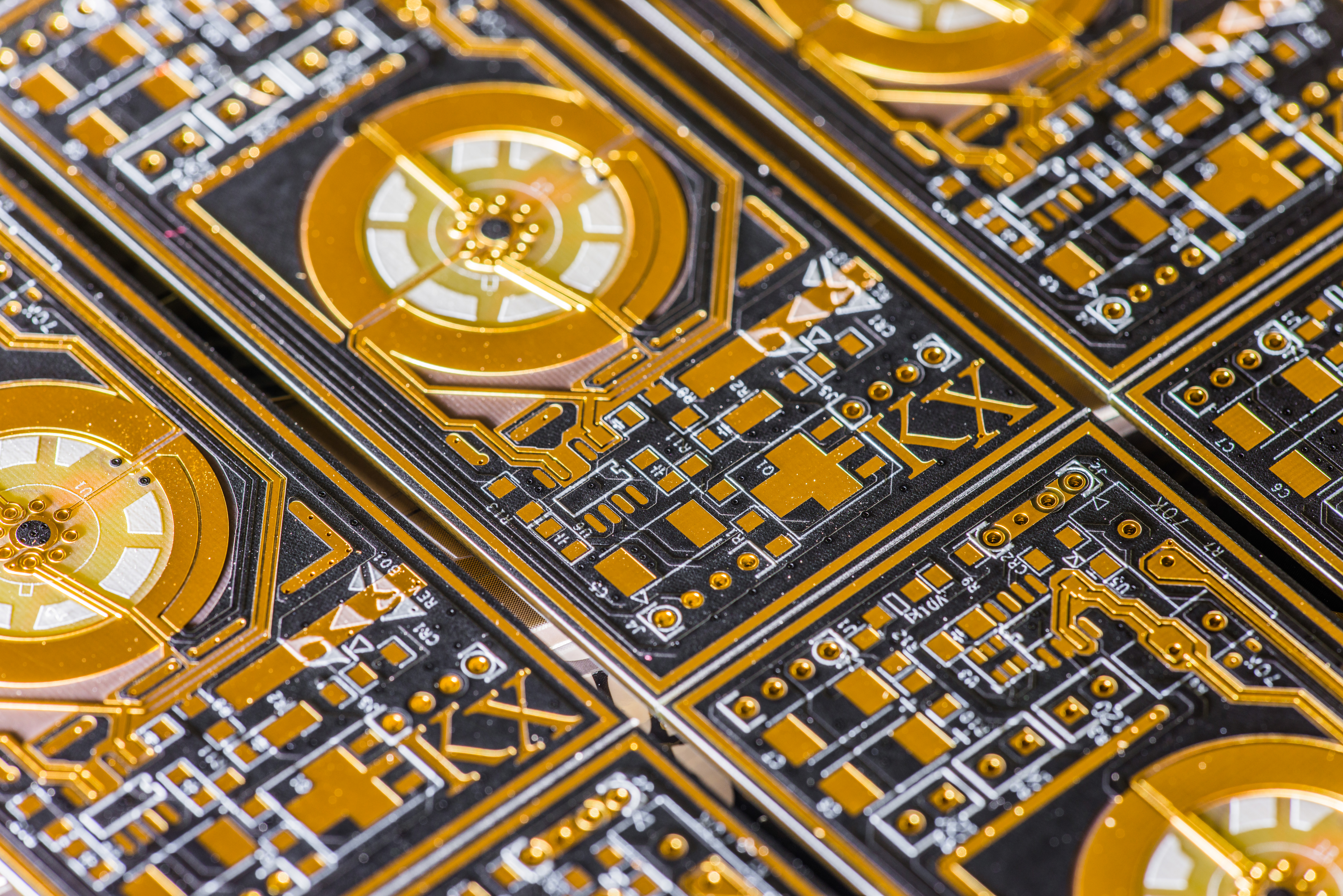
Image 6,7: xDevs.com KX voltage reference (Rev.B00) PCB overview, ENIG plating with solder mask
White silkscreen zones around LTZ denote copper-free keepout areas, so you can drill suitable sized holes there, if you like. It’s common thing to do for further reduction of mechanical stress to LTZ1000, even though effects of this are rarely visible on most of reference layouts.
U4 temperature sensor right near LTZ chip, on bottom side have additional thermal mass to center to provide closer temperature sense. While far from perfect, it still can be used as comparison temperature, for example between different temp setting points.
High impedance nets are surrounded by guard low-impedance track on both layers. That is targeted to improve long-term stability, as with time PCB surface will get more contaminated and absorb humidity and air dust particles.
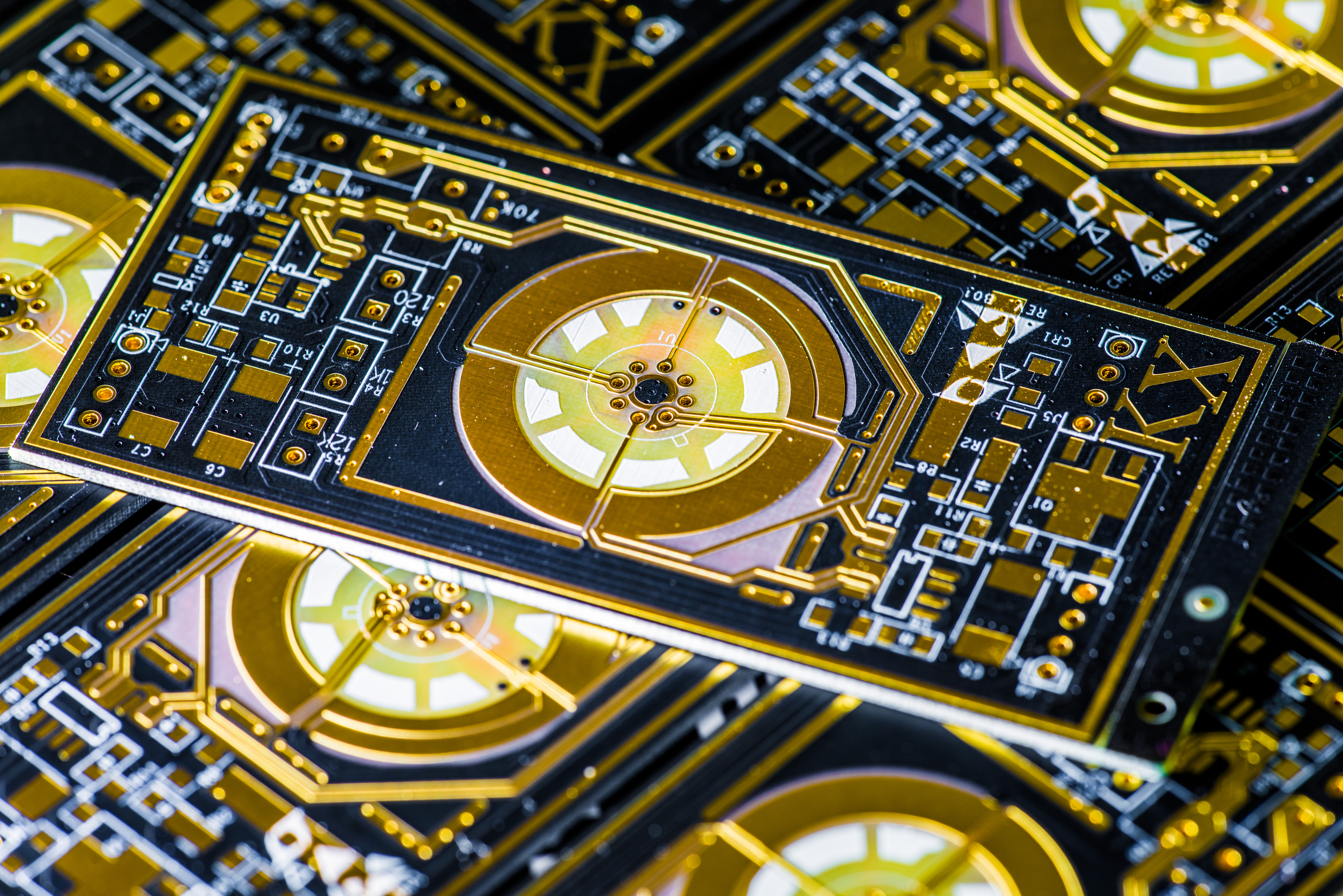
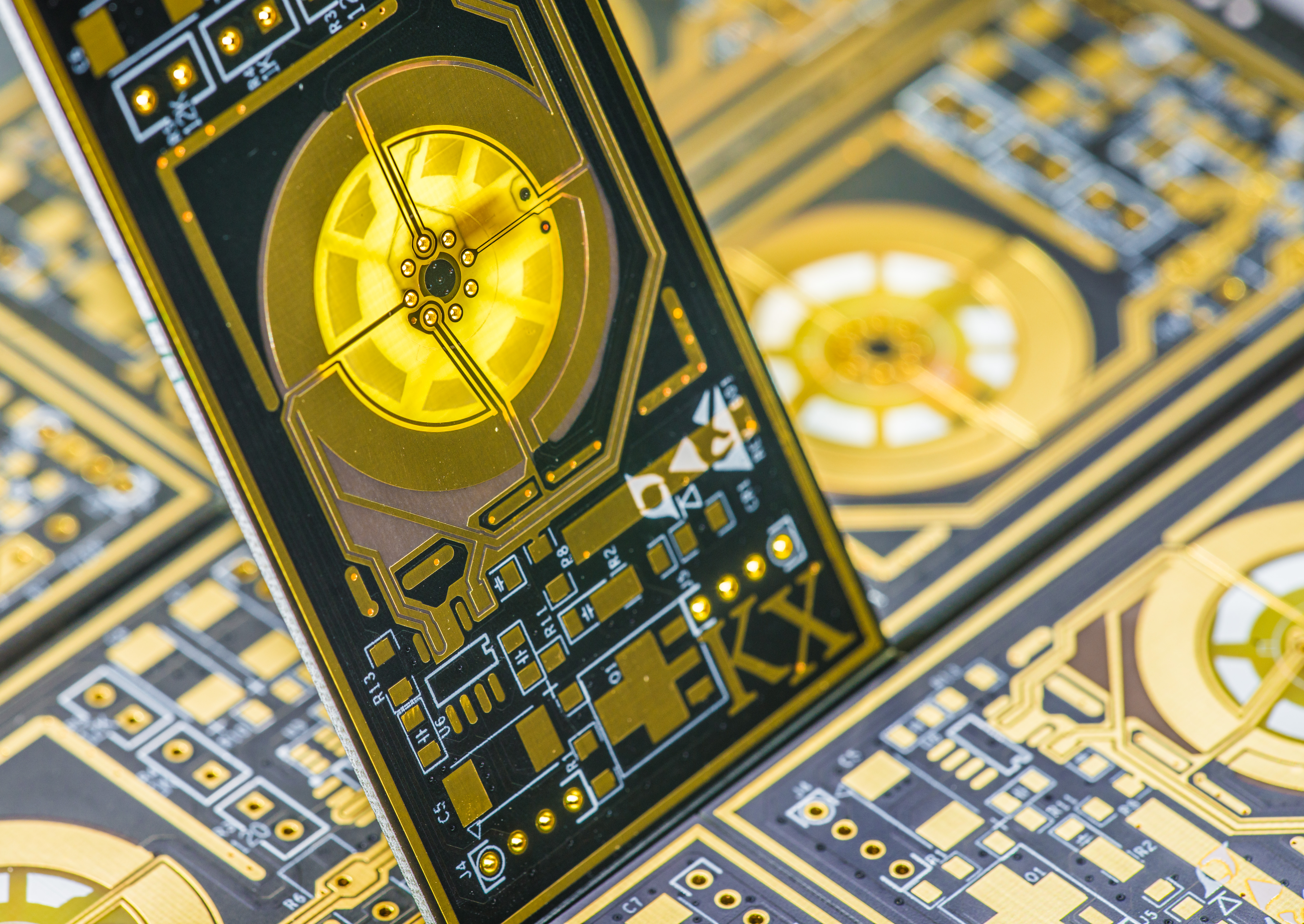
Image 8,9: xDevs.com KX voltage reference (Rev.B00) board photos
All parts are easy to solder using normal hardware tools, no tiny parts used. If film capacitors are used, suggest to preheat board and use wide thick tip to ensure best thermal transfer. This is important due to lack of thermal cutouts around pads, and film SMT-type capacitors have melting temperature below +170℃.
xDevs.com KX LTZ1000 reference PCB GERBER RS274X, Rev.B03
Gerber archive is password protected, just as measure that your read this article, before using it. Password is i_read_xdevs_com_guide.
PCB size is 3177 × 1575 mils, 4-layer on FR4 dielectric, with 55 ±5 mils thickness. Stackup Z-heights used are shown in this PDF. Output units are INCHES.
You can also order this latest Rev.B03 PCB from OSH Park for about $17 USD/pc. Project was created and ordered by one of EEVBlog members, SvanGool.
Assembly notes
Total BOM list of components used is listed in table.
| Qty | Value | RefDes | XPN | MFG | Desc | Footprint | Tolerance | Cost | Total | Digikey P/N |
|---|---|---|---|---|---|---|---|---|---|---|
| 1 | LTZ1000A | U1 | LTZ1000ACH | Linear | ULTRA-ZENER | TO5_8 | LTZ1000ACH#PBF-ND | |||
| 2 | 10 5% | R10,R11 | RC1206JR-0710RL | Yageo | RES 10 OHM 1/4W 5% 1206 SMD | 1206 | 5% | 0.00447 | 0.00894 | 311-10ERCT-ND |
| 1 | 1K 5% | R1 | RC1206JR-071KL | Yageo | RES 1.0K OHM 1/4W 5% 1206 SMD | 1206 | 5% | 0.00447 | 0.00447 | 311-1.0KERCT-ND |
| 1 | 1M 5% | R8 | RC1206JR-071ML | Yageo | RES 1.0M OHM 1/4W 5% 1206 SMD | 1206 | 5% | 0.00447 | 0.00447 | 311-1MRCT-ND |
| 3 | HDR4_2.54 | J1,J2,J4 | TSW-104-17-G-S | Samtec | CONN HEADER 4POS .100 | con_hdr4 | 1.1 | 3.3 | SAM1061-04-ND | |
| 2 | MAX6610AUT | U3,U4 | MAX6610AUT | MAXIM | Thermal sensor IC | SOT23_6 | 1.82 | 3.64 | MAX6610AUT+TCT-ND | |
| 3 | 47uF | C5,C6,C7 | T495×476K035ATE300 | Kemet | CAP TANT 47UF 35V 10% 2917 | 7343p | 10% | 1.904 | 5.712 | 399-3905-1-ND |
| 2 | LTC2057IS8 | U5,U6 | LTC2057IS8 | Linear | IC OPAMP ZD 1.5MHZ 8SOIC | so8 | 3.29 | 6.58 | LTC2057IS8#PBF-ND | |
| 1 | 400K | R2 | ERA-8AEB4023V | Panasonic | RES 402K OHM 1/4W .1% 1206 SMD | 1206 | .1% | 0.3714 | 0.3714 | P402KBCCT-ND |
| 4 | 0.1UF | C1,C2,C3,C9 | LDEDB3100JA0N00 | Kemet | CAP FILM 0.1UF 63VDC 1210 | C1206 | 5% | 1.139 | 4.556 | 399-6417-1-ND |
| 1 | 10K | R13 | TNPW120610K0BEEA | Vishay Dale | RES SMD 10K OHM 0.1% 1/4W 1206 | 1206 | 0.1% | 0.69 | 0.69 | TNP10.0KACCT-ND |
| 1 | 0.01UF | C8 | ECH-U1H103JX5 | Panasonic | CAP FILM 10000PF 5% 50VDC 1206 | C1206 | 5% | 0.47 | 0.47 | PCF1340CT-ND |
| 2 | 1N4148 | CR1,CR2 | 1N4148UR-1 | Microsemi | DIODE SW DO-213AA | 1206 | 2.03 | 4.06 | 1N4148UR-1-ND | |
| 1 | PZT3904 | Q1 | PZT3904 | Fairchild | TRANS GP NPN 40V 200MA SOT223 | SOT223 | 0.362 | 0.362 | PZT3904CT-ND | |
| 1 | 22nF | C4 | FCP1206C223J-H1 | CDE | CAP FILM 0.022UF 5% 16VDC 1206 | C1206 | 5% | 0.67 | 0.67 | 338-4081-1-ND |
| 1 | 120 | R3 | Y1073120R000B | Vishay | Z202 | r_z202 | 0.01% | 38 | 38 | |
| 1 | 1K | R4 | Y10731K00000T | Vishay | Z202 | r_z202 | .01% | 38 | 38 | |
| 1 | 13K | R5 | Y107313K0000T | Vishay | Z202 | r_z202 | .01% | 38 | 38 | |
| 2 | 70K | R6,R7 | Y607270K0000T | Vishay | VHP203 | r_vhp203 | 0.1% | 51 | 102 | |
| Total, $USD | ~325 |
Table 7: xDevs.com KX VREF B03 BOM-list with estimated cost per each part
Linear parts were purchased directly from their website shop, Bulk Metal Foil resistors were ordered from Vishay Precision Group, rest of parts come from Digikey USA.
Assembly small passive components, such as capacitors, SMT resistors first. Install diodes and power transistor Q1. Then you can install temperature sensor ICs U3 and U4. You can test temperature sensor operation by connecting power supply to J5 port and measuring temperature outputs at J4.
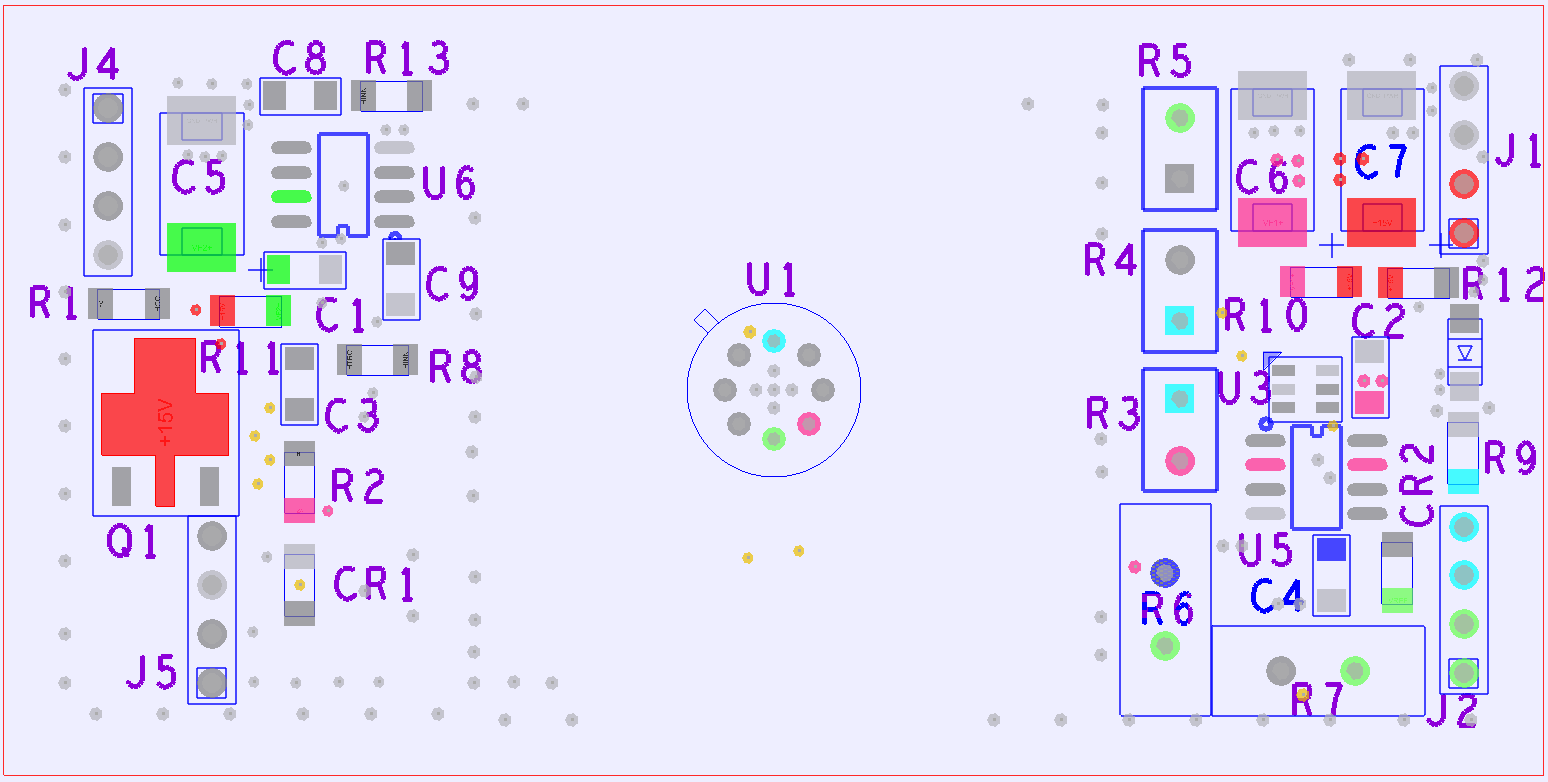
Image 10: xDevs.com KX reference assembly top component locations
Solder op-amps and clean board thoroughly. Suggest using clean isopropyl alcohol to clean board from oils and flux. Using gloves from this point would be not a bad idea. After this, you can install and carefully solder precision resistors and LTZ1000ACH or LTZ1000CH. If you use LTZ1000CH (without letter A), resistor R2 is required. If LTZ1000ACH used, R2 should be unpopulated. A-version have much better thermal insulation between die and case and require significantly lower power to maintain set-point oven temperature. It could be important factor for battery-powered reference or portable transportable projects, as example.
Voltage reference module xDevs.com KX designed for education and hobby experimentation purposes only, which resulted in very specific bias and used components choices. If one need ultra-stable voltage reference for production device or practical equipment, very different approach would be required. This includes adding necessary polarity/overload/ESD protection circuits to the input and outputs of the reference, using much cheaper 65-80 KΩ well sufficient metal film resistors for 70 KΩ instead of very expensive metal foil, using traditional LT1013 opamp without chopper current noise, using robust thru-hole film capacitors instead of easy to damage SMT film type.
To reduce thermal stress to foil resistors, heatsink legs with small pliers or braid during soldering, so resistor body would not heat up as much. Excessive heat on resistive element will cause stress and possible hysteresis, which will require long-term recovery to original state afterwards. Make your soldering brief and short. If solder joint not good, wait till board and resistor cool down back to ambient and then try brief reflow for bad connection again. Do not keep iron tip heating up resistor lead longer than few seconds.
Bottom side have only one chip, temperature sensor U4 under LTZ1000 package area. This is best to solder before LTZ1000 installed.
Assembly top view, PDF-format drawing
Assembly bottom view, PDF-format drawing
After assembly complete, clean everything again with IPA. Avoid using ultrasound bathes, as they could cause excessive stress to precision parts. Do not touch board surface wire bare hands after cleaning, handle modules only by PCB edges.
Make sure you installed copper short at R9 location, which connects signal ground to power ground, otherwise reference module will not work correctly!
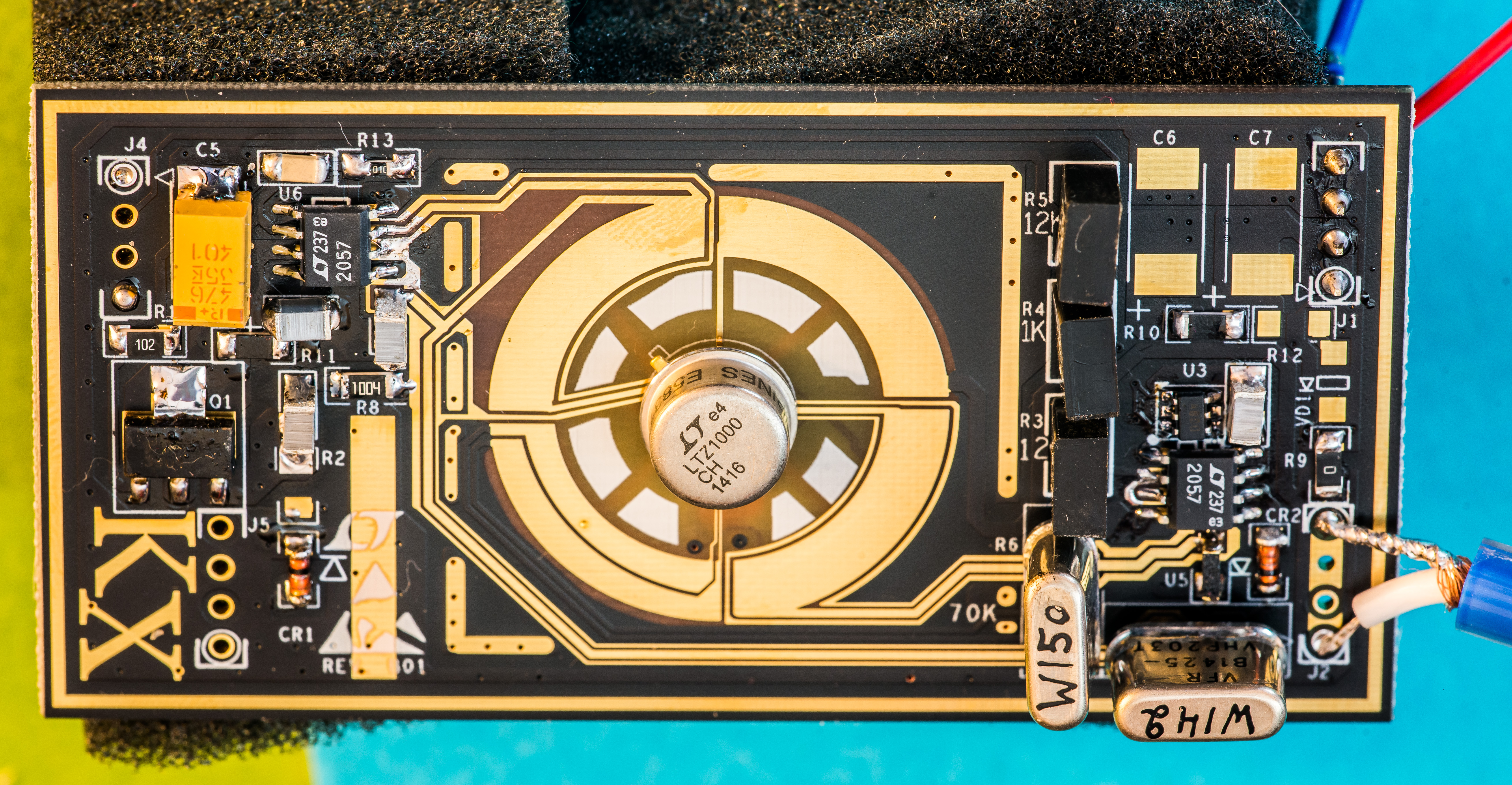
Image 11: xDevs.com KX voltage reference (Rev.B00) right after assembly, LTC2057 + Vishay Precision Foil resistors
Now it’s ready to test. But before this, worth to note few design concepts regarding LTZ1000 based reference (most of which apply to many other similar high-precision analog designs).
Valuable considerations while building and using ultra-precision references
While ppm-precise level parts such as the LTZ1000 easy to buy, building a system to benefit LTZ1000’s performance is not an easy task. Common error sources in precision circuits are thermoelectric voltages, noise, temperature drift, humidity/pressure and even physical stress. Proper assembly techniques with care about thermal, mechanical and overall placement should be followed to reduce coupling and propagation of these errors on sensitive circuits. It is important to shield precision analog parts from external electromagnetic, thermal and airflow interference. These considerations will be summarized here briefly.
Aging and long-term stability
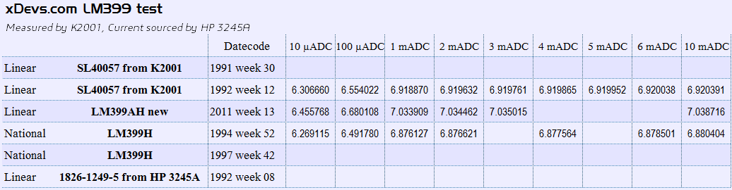
Aging of LTZ1000-based reference module heavily depends on selected operation temperature point. References are not being powered on constantly age significantly less. Measurements for aging are often tricky down at sub-ppm levels. Most simple is to direct measure zener voltage with precision voltmeter. But it’s also least accurate, as if noise or voltage deviation was seen, it is not certain what is a root cause of such, either zener under test or reference zener in voltmeter itself. Most of industry standard 6½ DMMs using LM399, while 7½ and 8½ usually embed LTZ1000A reference.
Another, more accurate, approach is to use another known-stable well-aged 10V standard, divided down to approximate DUT reference voltage (for example 7.1V) using stable resistor divider or KVD. Now this divider voltage can be compared with DUT zener voltage output using lowest DMM range (such as 100 or 200mV), effectively improving resolution to 10nV, if using 7½-digit DMM, instead of 1 µV for 10V range. Voltmeter must be with very high impedance inputs to avoid loading errors. To ensure confidence in measurements it’s recommended to have multiple 10V standards, which must be frequently compared and assigned their output values, so overall system drift would correlate with measurements.
Noise generation and pickup
When operating with microvolt-accurate voltages, it is of great importance to keep noise levels to a minimum. Typical power supply can easily radiate noise with magnitude of millivolts, while our circuit is sensitive down at microvolts. The noise spectral density of used amplifier, Johnson noise of resistances can affect final performance of circuit. Proper reference buffers with low specified noise density, good long-term stability, low tempco and high CMRR:“PSRR”:https://en.wikipedia.org/wiki/Power_supply_rejection_ratio are required for maximum performance. The most effective method of minimizing noise – ensure that it is never introduced into the circuit in the first place. Check stability of circuit operation, avoid stray capacitance on circuit nodes to ensure reference is DC-stable.
But even with no noise generated by reference itself, it is important to avoid pickup of radiated and induced external electrical interference, for example from near-by switching DC/DC or mains transformer. Protection techniques, such as shielding, guarding, and great care to grounding and proper PCB wiring techniques are imperative. Isolate any high-current flows from reference power supply and output path. Both chassis (including the tops cover, if installed) should be grounded to provide shielding against outside interference. This is also true for the braid of the cable leading the current to the load. Whenever possible, the current should be carried by a twisted pair configuration to prevent low-frequency noise pickup from stray magnetic fields.
Thermoelectric voltages
Thermoelectric voltages are direct result of the Seebeck effect. This is exactly how thermocouple sensors work – two dissimilar metal junctions generate small voltage EMF. Depending on the metals of the junction, this EMF can vary from 0.1 µV/°C to values over 1 mV/°C. In best case, direct copper-copper junction, EMF would be less than 0.1 µV/°C. In the worst case, such as copper-copper-oxide this voltage can be as big as 1 mV/°C!. This sensitivity to even very small temperature variations directs to possibility of temperature gradients forming around dissipative components, such as power transistor or resistors. Even slow-moving air currents, which in turn generate varying thermoelectric voltages can be visible as a low-frequency drift similar to 1/f noise. Thermoelectric voltages can be reduced by ensuring that there are no dissimilar junctions in the system and/or eliminating possibility of thermal gradients. It is virtually impossible to eliminate different metal junctions, as many different metals exist in IC package (covar pins, gold bond wires, copper frame), PCB (copper, tin solder, nickel, gold plating), wiring (copper, tin), and connectors (brass, gold plating, copper). One way is to keep all these junctions clean and oxide-free, and equalize their temperature as close as possible. Enclosing the circuit to plastic shielded enclosure to isolate it from air currents would be an effective thermoelectric voltage stabilizing method, and it could have the added value of providing electrical shielding. More extreme ways are to use Dewar-based enclosure with low thermal conduction, as well using oven around whole circuit to keep temperature static.
Temperature coefficient and drift
As with any high-precision design, temperature-related drift of used components is a major source of errors. Minimizing this issue is possible by choose critical components with below 1 ppm temperature coefficients. Very low drift, better thermally matched resistor networks should be used for scaling and gain circuits, such as 7V->10V. Precision wire-wound Evanohm® or bulk metal-foil resistors can have required level of temperature coefficients, often below 1ppm/K.
Physical stress and piezoelectric effects
Most of parts are sensitive to stress on their package. Stress often can be caused by flexing of the PCB, vibration (such as from DC fan motor nearby), tight mounting on chassis and thermal expansion/contraction stress after soldering. For large printed circuit boards, more stress can be generated to package. Precision circuits on such designs usually placed in small stress-relieved isolated area to allow less rigid coupling to rest of chassis/board. Our reference is designed on separate module, so connection to larger main board can be performed using flexible interfaces such as flexible wiring. Ceramic capacitors may often have piezoelectric effect, visible by generated EMF due to physical stress on them. Film capacitors can be used instead to mitigate this issue.
Long-term stability
High precision parts, such as Linear LTZ1000 is very stable device, but still affected by physical long-term effects, which cause age-related changes. Long-term stability also depends on operation conditions, if device is running powered and operation temperature greatly affects long-term drifts. It’s very hard to accurately predict drift rate of each particular sample, but overall observations of many LTZ-based referenced concluded higher long-term drift with high set-point temperature with non-stop operation. If you use your reference rarely, for example having it in DMM, it’s not a bad idea to keep it mostly off, and turn on instrument only when needed. Proper warm-up time at least few hours should be granted to get unit reach operation conditions and temperatures.
Overall module construction and assembly
Pay great detail to your the power supply and ground return connections and layout, to ensure performance. Use module such that the high-current heater section and precision sense sections are physically separated and confined to separate areas of the board. If multiple devices require an ground connection, establish the connection at one point only, usually at power supply or DAC/ADC system. There should be good power supply bypassing of at least 10 µF in parallel with smaller 0.1 µF on supply input terminals, as close to the module as possible, ideally right up against the device. The 10-µF capacitors should be of the low-ESR aluminum or tantalum type, or large-size (1210 or bigger) ceramic type with high enough voltage rating. The 0.1-µF capacitor can be smaller 0805 or 0603 size, with low ESR and ESL. Small series ferrite bead on power supply input can further help to isolate high-frequency noise from the device.
The power supply traces should be as wide as possible to provide low-impedance path and reduce the sags and voltage drops on the power-supply line. Avoid routing fast-switching digital signals, clocks, serial interfaces to avoid radiating noise into reference module. Noisy digital or power traces should never be near the reference outputs or under the module. Do not power reference module from DC/DC switching supplies, as they usually have excessive noise, which is very difficult to filter out. Use good low-noise linear LDO regulator after separate low-noise switching supply if you have no better power available. Impact of power supply quality can be easily verified by using regular 12V battery pack from car or motorcycle.
Initial data results
Connect power to the modules from quiet (electric noise wise) linear power supply, leave to settle for few days/weeks/months and then measure with best stability multimeter available.
Make sure power supply polarity is correct before power on.
Reverse polarity even for brief seconds can reliably destroy expensive LTZ1000 chip.
Here are some measurements and test data completed on 5pcs LTZ1000 modules:

Table 8: xDevs.com KX reference modules test with K2001
All five modules were installed in plastic box, to avoid air movement.

Image 12: Modules in plastic enclosure during initial test run
Measured by Keithley 2002 with 2001-TCSCAN 10-channel card:

Image 13: Keithley 2002 DMM with scan card and temperature monitor Omega CN3800
| Scan number | PCB revision | Used reference, amp | Temp setpoint | Output voltage via K2002 |
|---|---|---|---|---|
| Channel 2 | Rev B01 PCB | LTZ1000CH, LTC2057, | 12K/1K heater | 7.1304749 VDC reference |
| Channel 3 | Rev A01 PCB | LTZ1000ACH, LTC2057, | 13K/1K heater | 7.1367946 VDC reference |
| Channel 4 | Rev B01 PCB | LTZ1000ACH, LTC2057, | 13K/1K heater | 7.1585775 VDC reference |
| Channel 5 | Rev A01 PCB | LTZ1000ACH, LT1097, | 13K/1K heater | 7.1366038 VDC reference |
| Channel 6 | Rev A01 PCB | LTZ1000CH, LTC2057, | 12K/1K heater | 7.1296732 VDC reference |
Table 9: Test run samples result, 5pcs
Thermal analysis
Verification with thermal imagery was performed to evaluate thermal gradients over assembled module. Main focus was at precision resistors and reference temperatures. Please note, that surface temperature of LTZ can does not indicate actual die temperature, as thermal resistance even for regular LTZ1000CH is no less than 80°C/W.
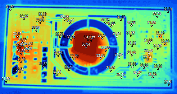
Image 14: Thermograph of assembled prototype module
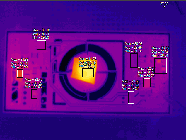

Image 15,16: Thermographs of assembled prototype module
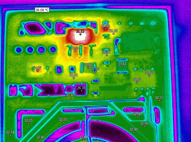

Image 17,18: Thermographs of assembled prototype module
Test chamber design
To measure tempco of whole module, I had designed small aluminum enclosure with test ports to allow temperature variation of module and temperature coeffient measurements.
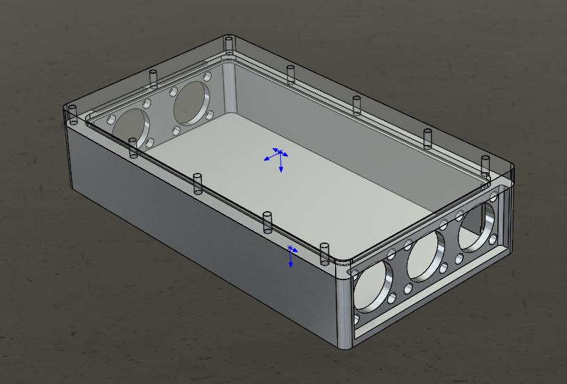
Image 19: Chassis CAD 3D rendering
Here’s prototype chassis made using CNC from aluminum block:
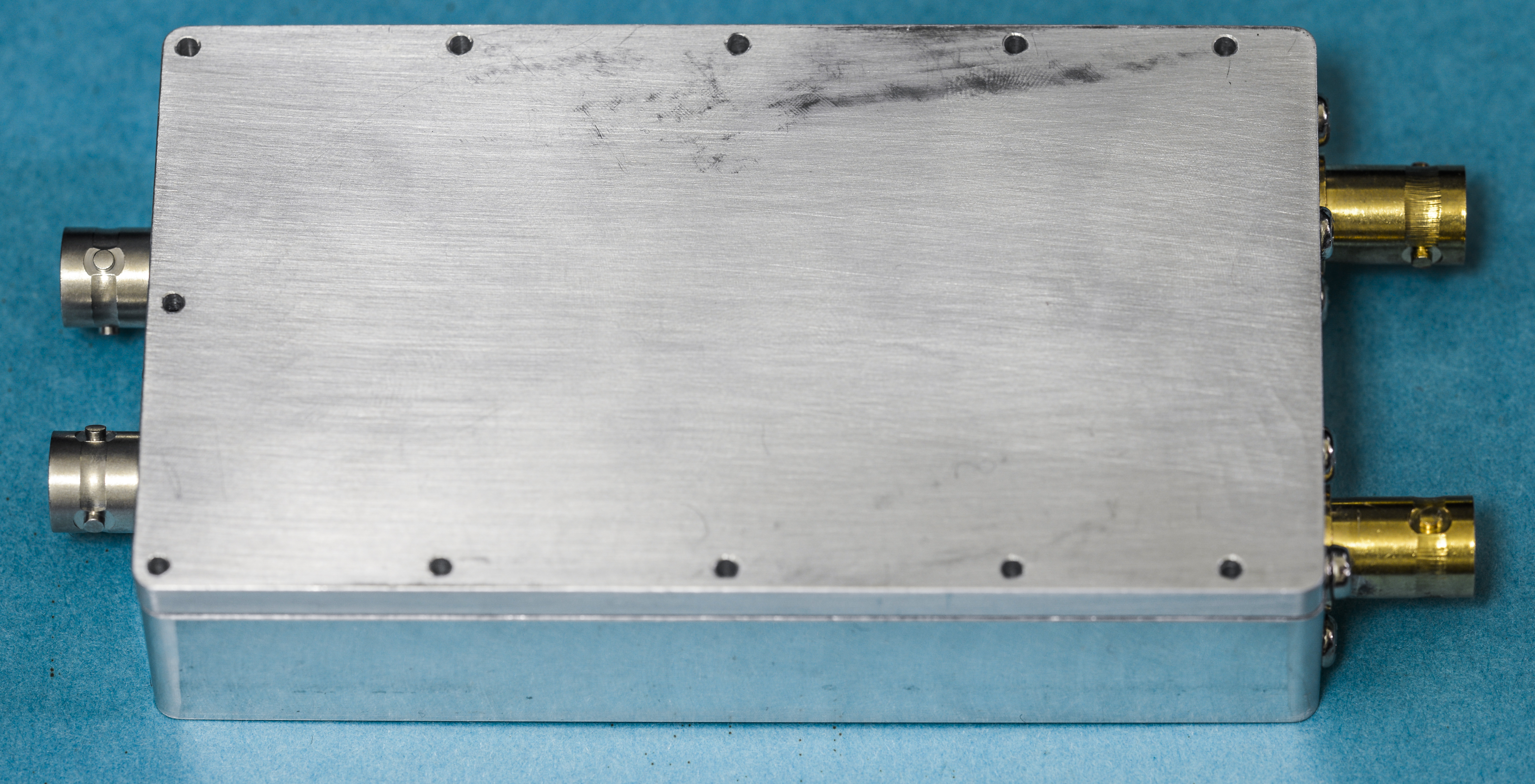
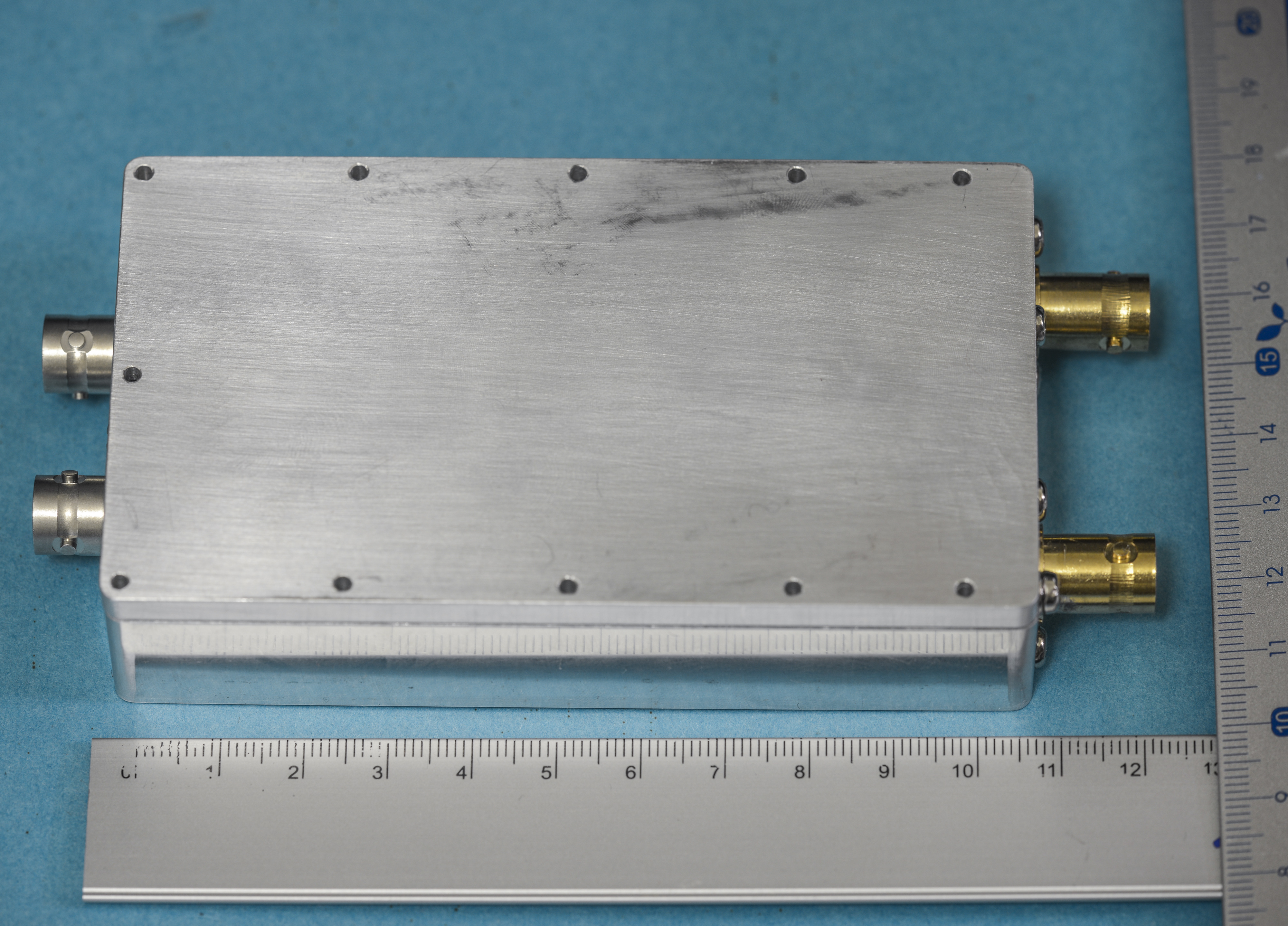
Image 20,21: Actual CNC chassis sample photographs
With Dual LM399+7V/10V/20V ratio board
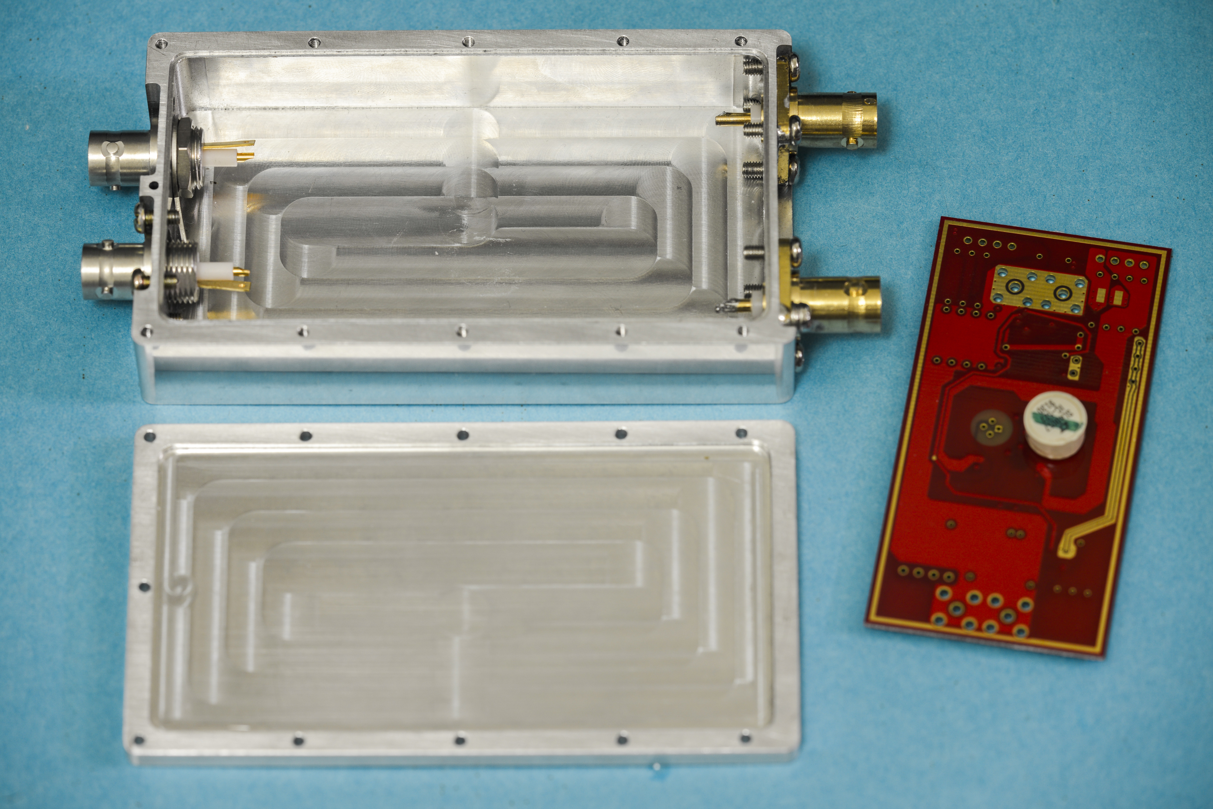
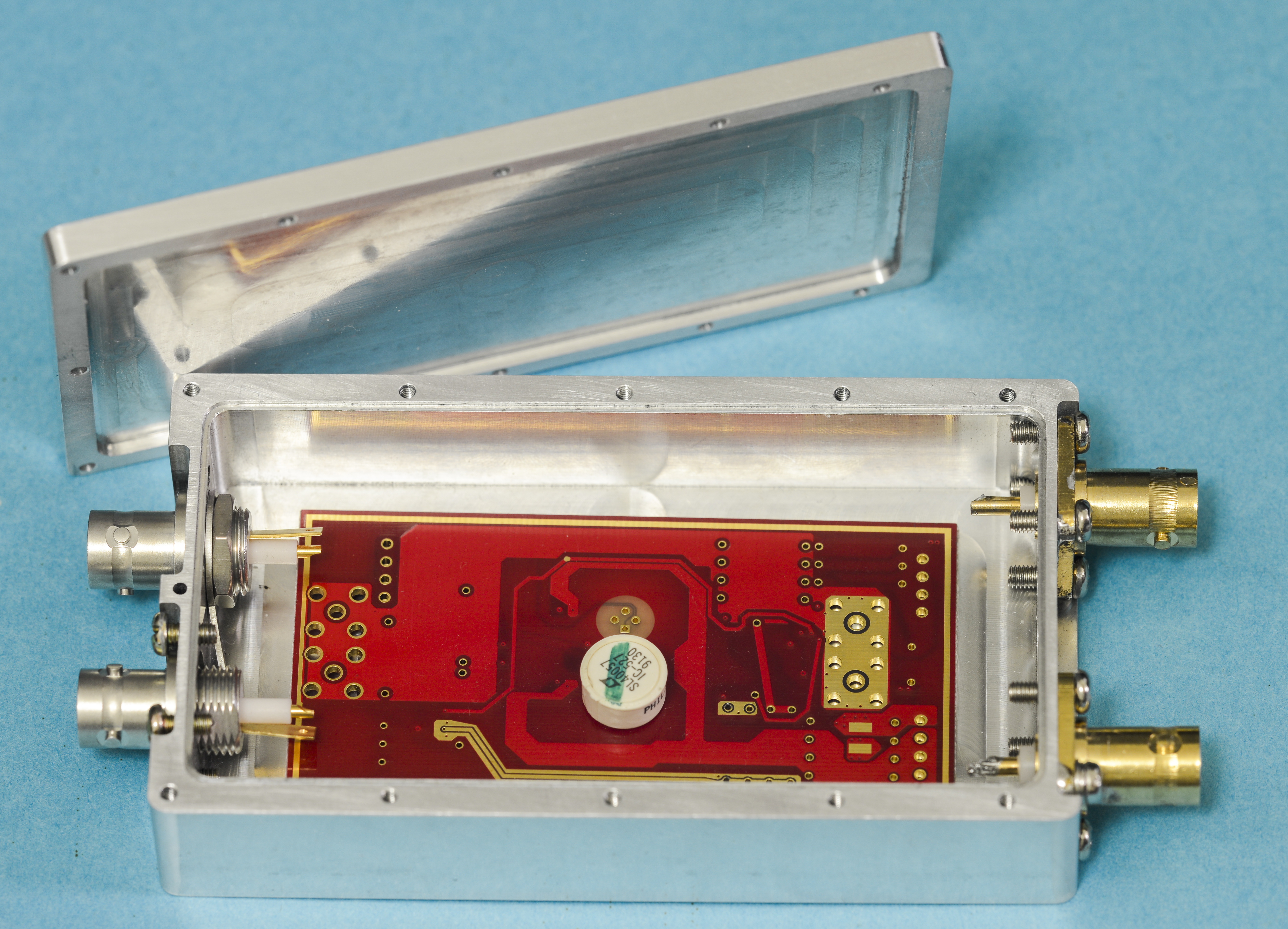
Image 22,23: Chassis features
With LTZ1000 board. Variants of TRX input connectors mount.
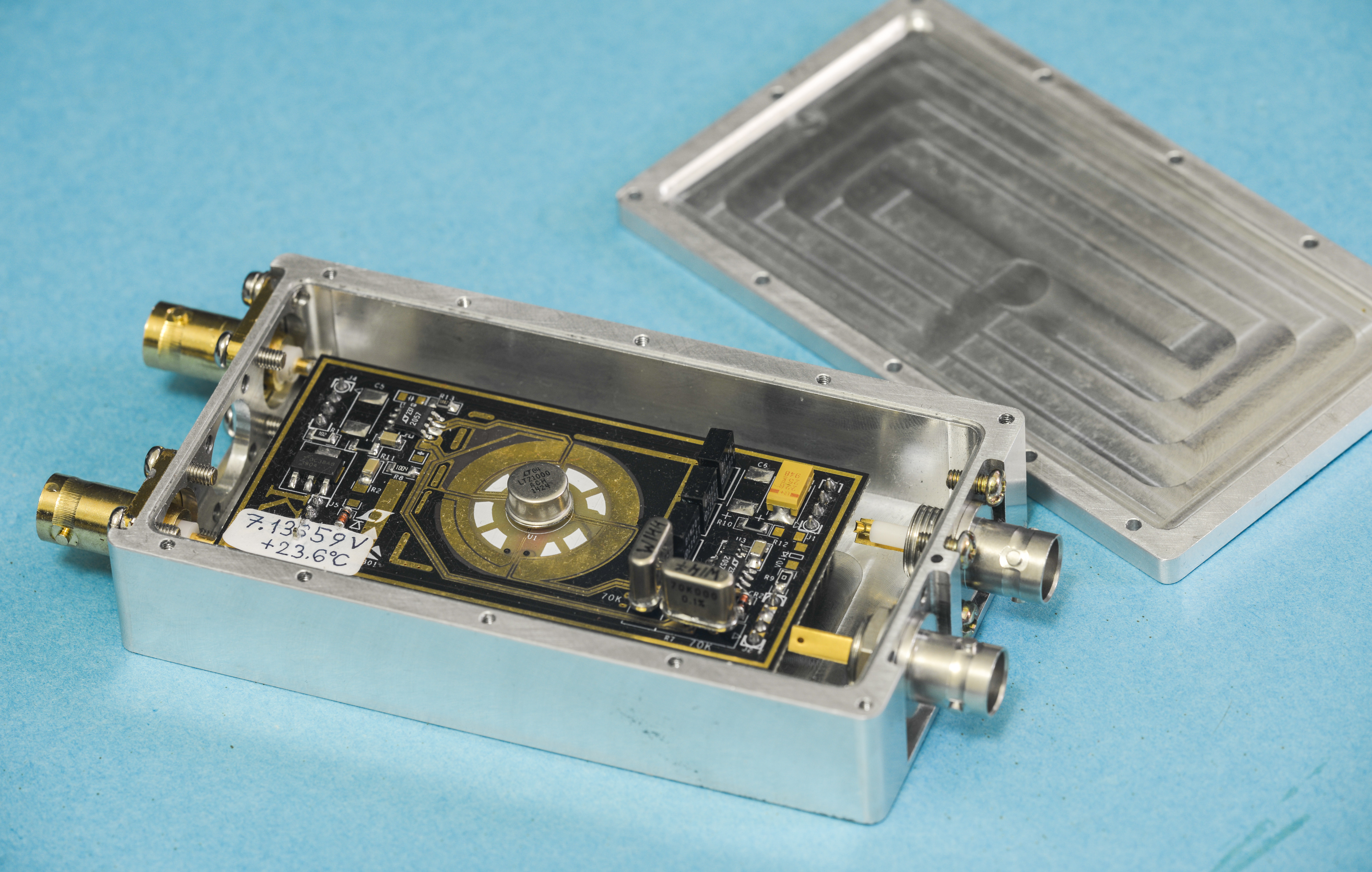
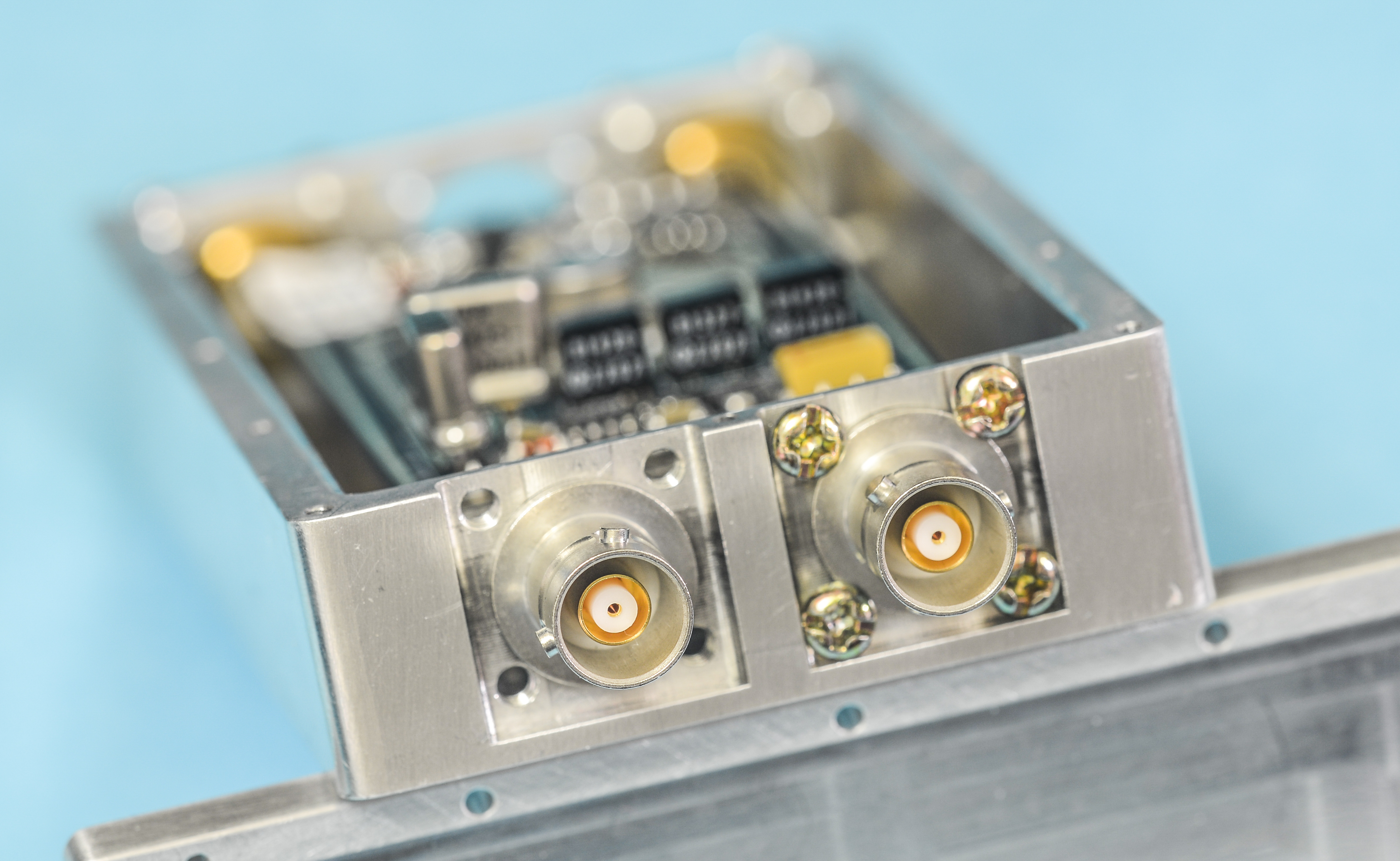
Image 24,25: Input and output ports, suitable flange mount with M3 threaded holes
BNC and TRX in chassis locations
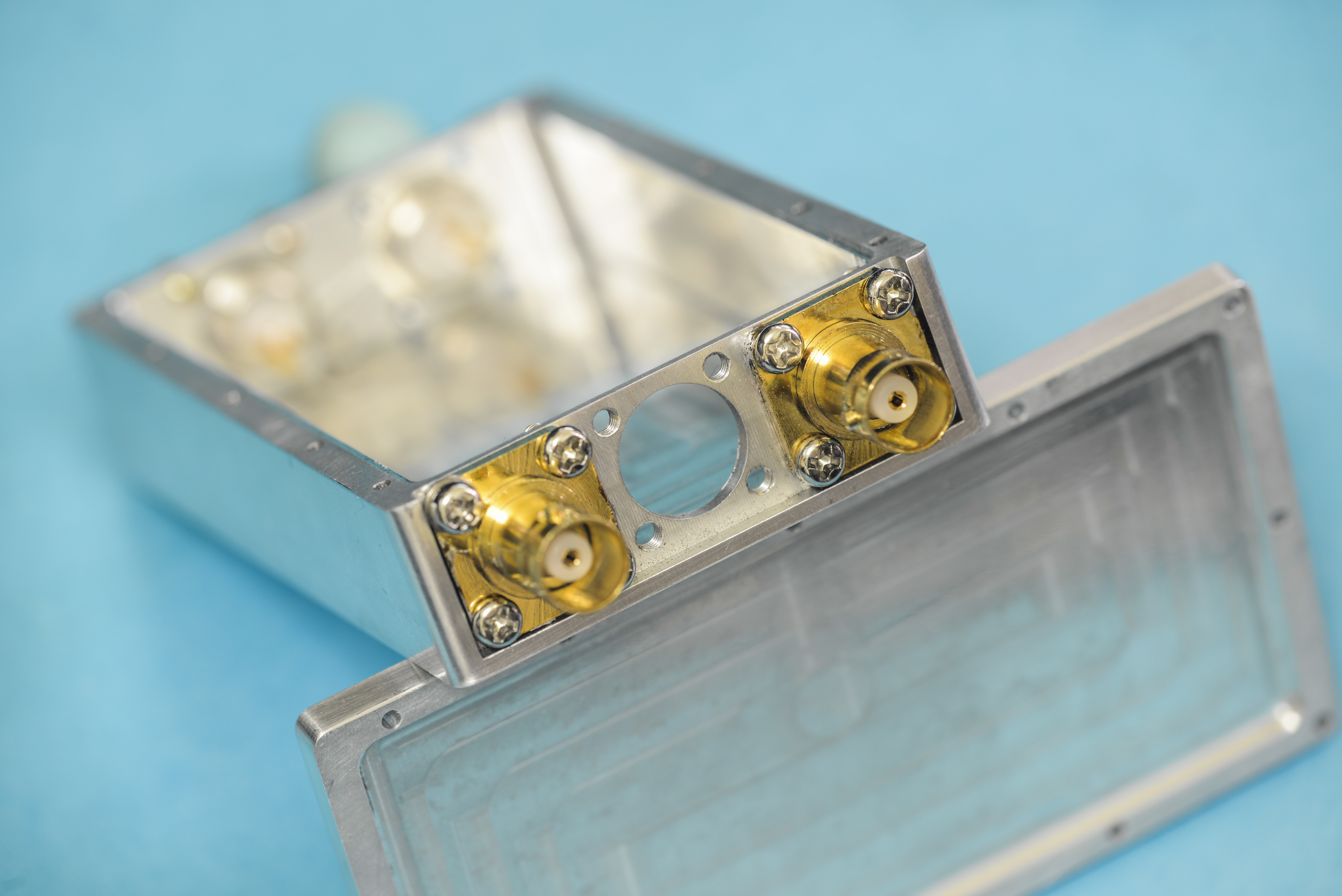

Image 26,27: Chassis features
Overall:
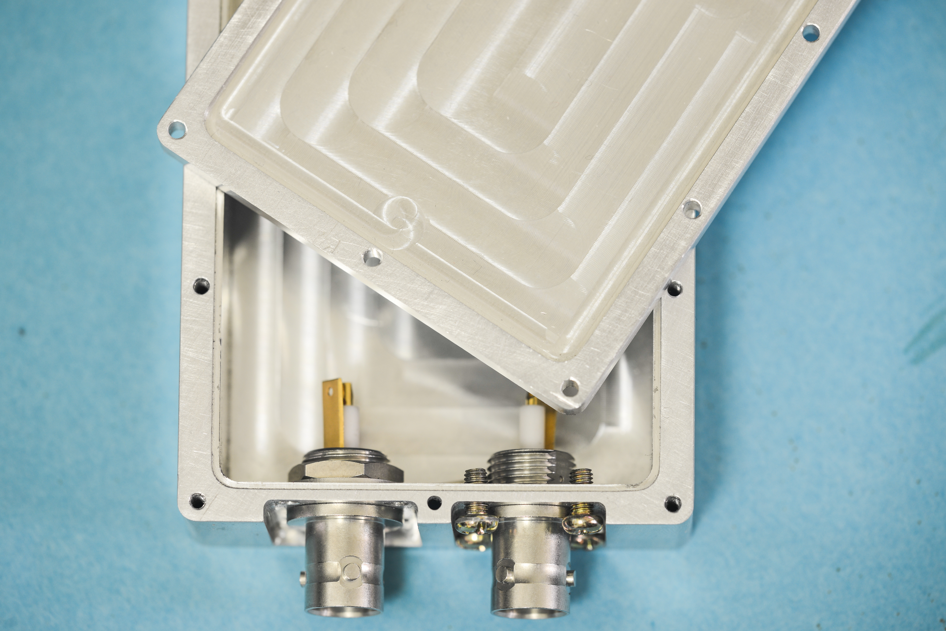
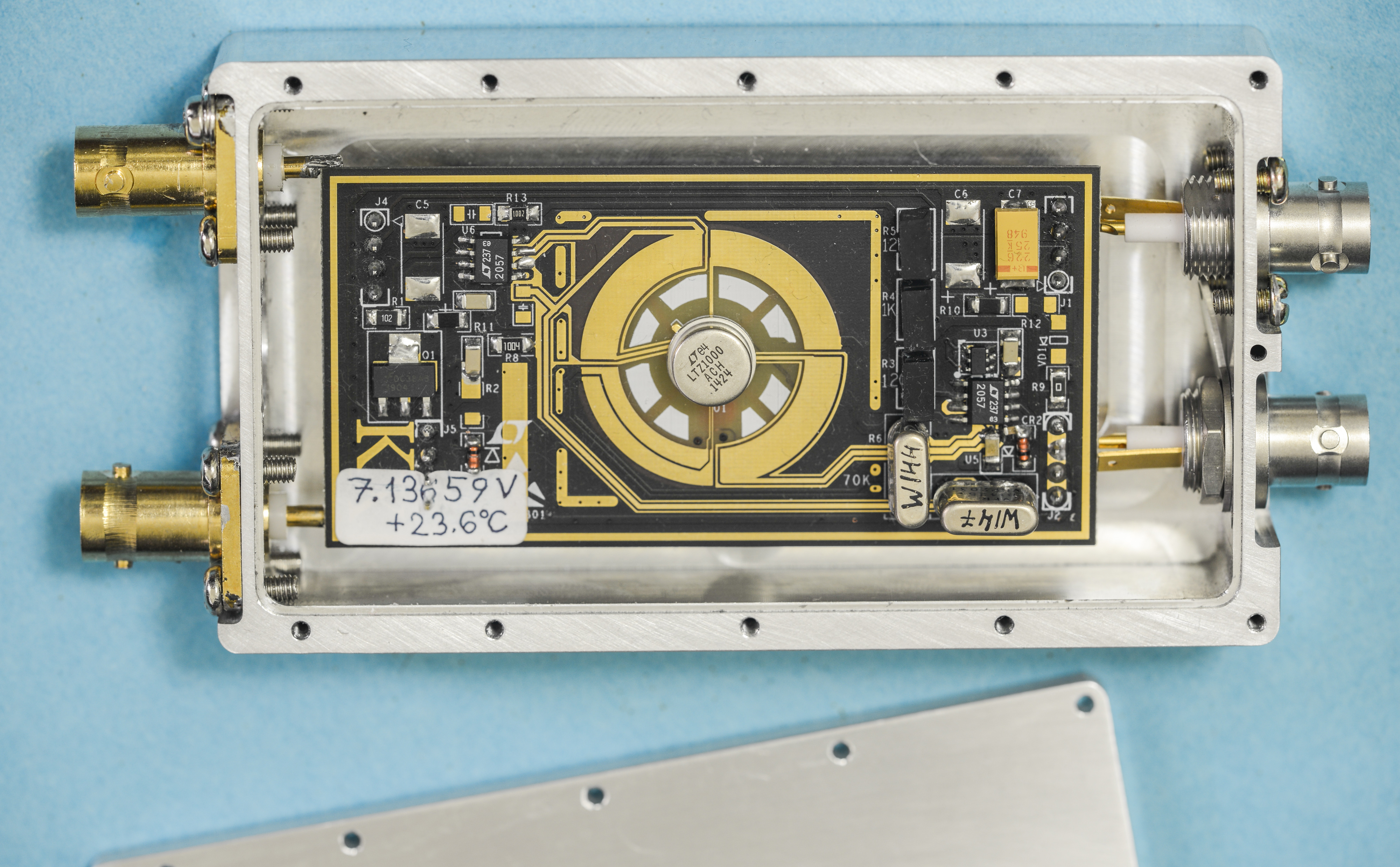
Image 28,29: Chassis with module in it
Chassis can accept TEC module on outer side to control temperature, so internal board can be varied in temperature.
Here is another chassis example with xDevs.com LTZ1000A reference prototype board:
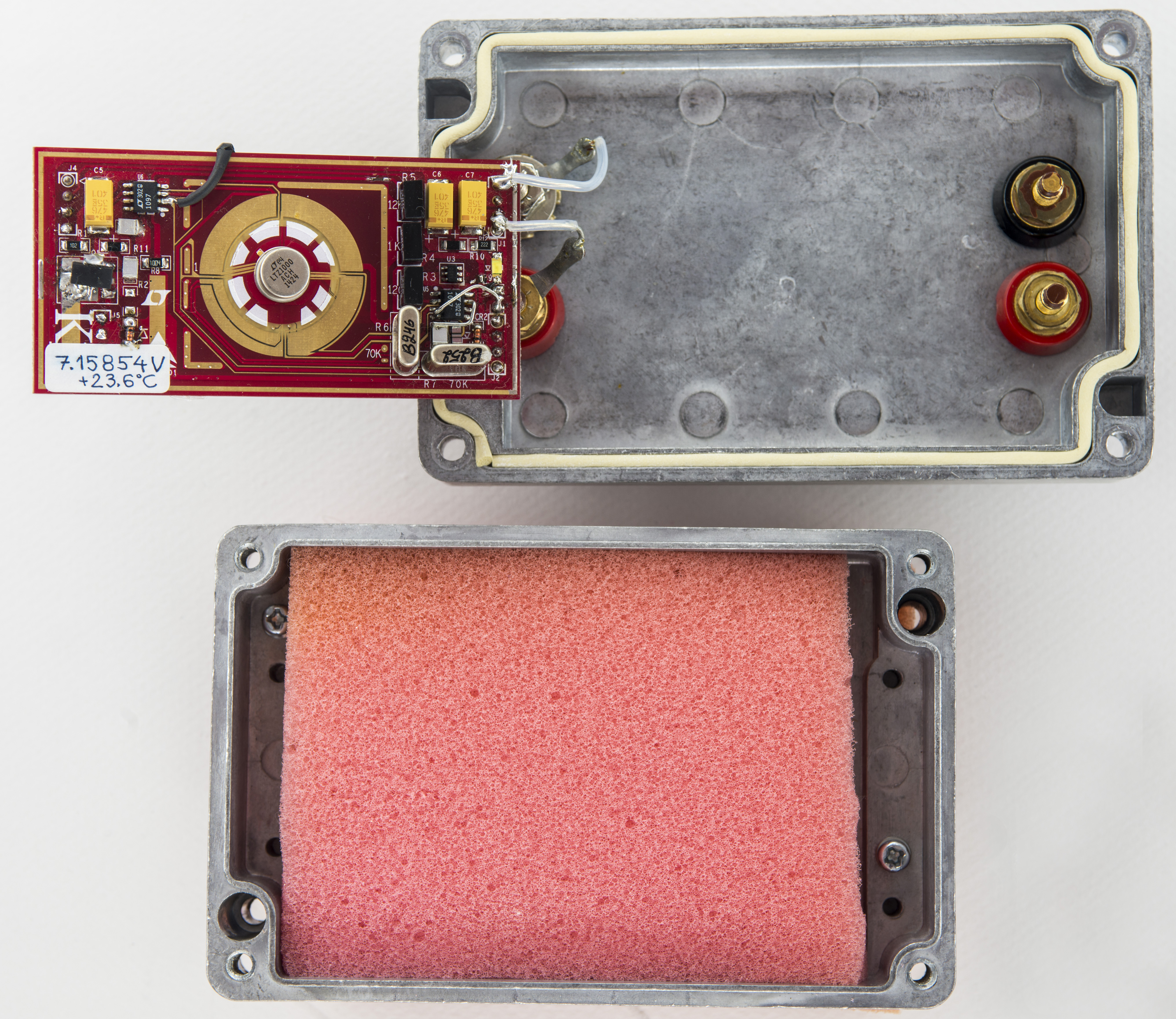
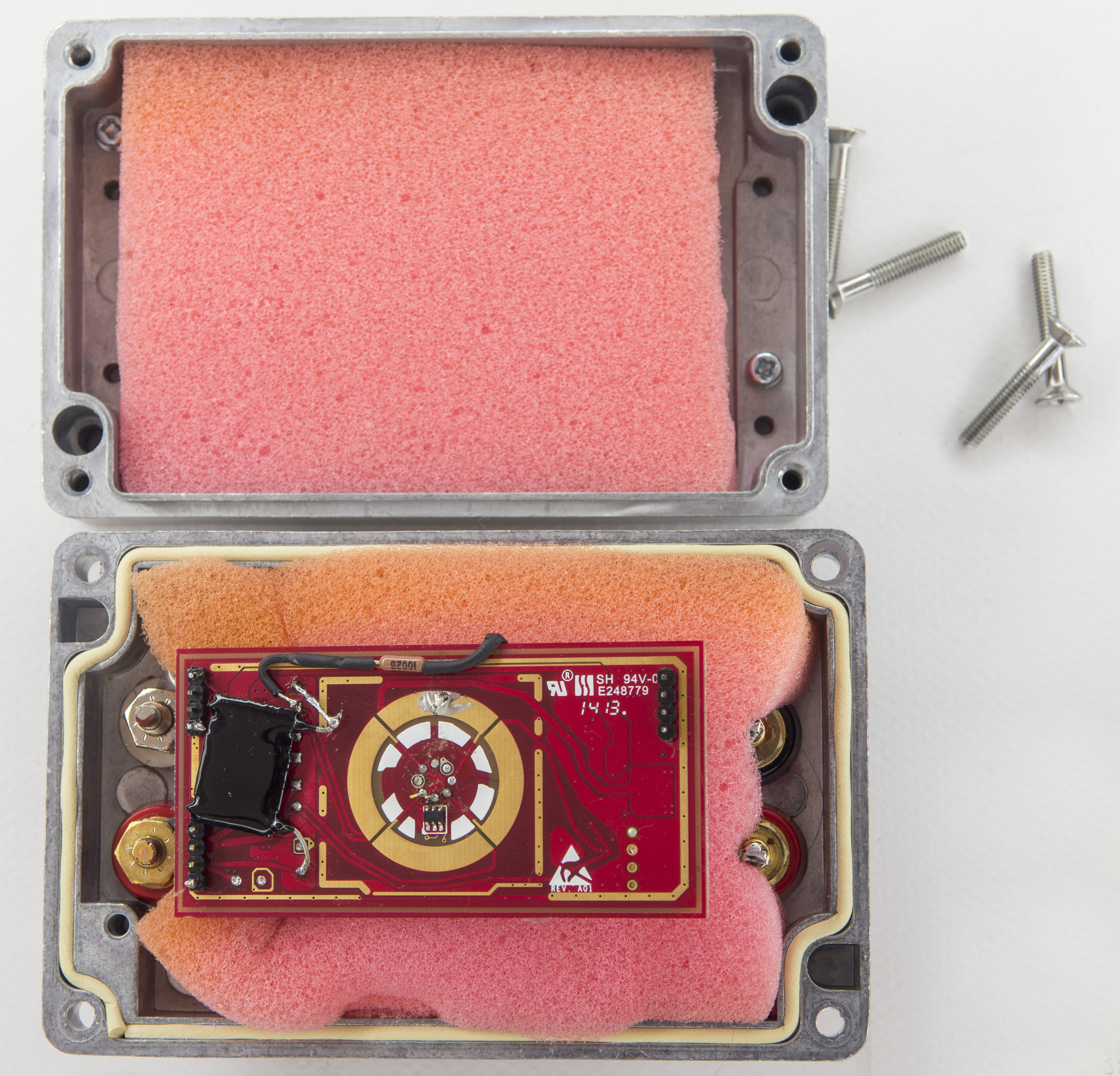
Image 30,31: Module assembly in cast metal chassis for portable 7V reference
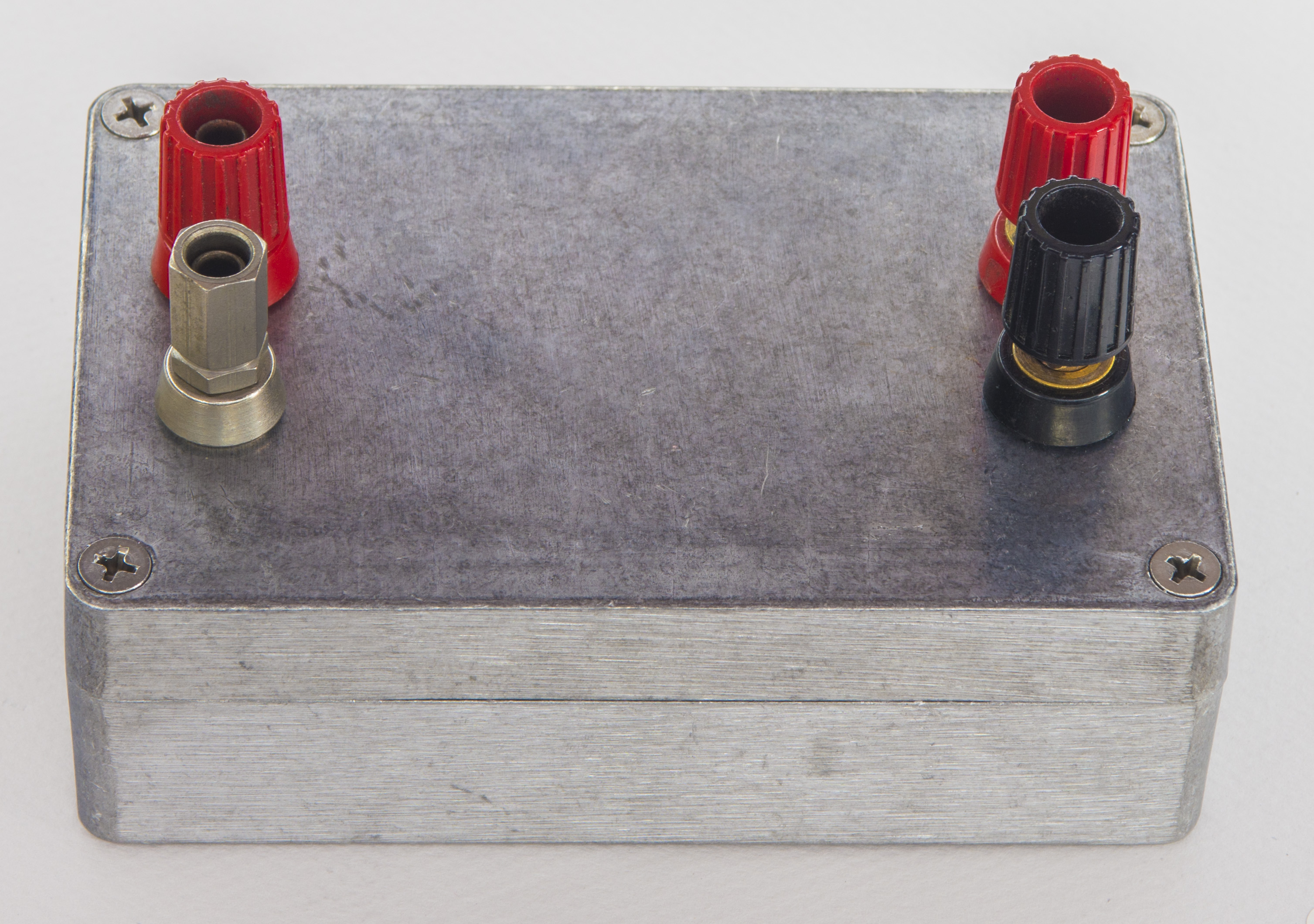
Image 32: Assembled chassis with input power and output jacks
Temperature coefficient measurements and analysis

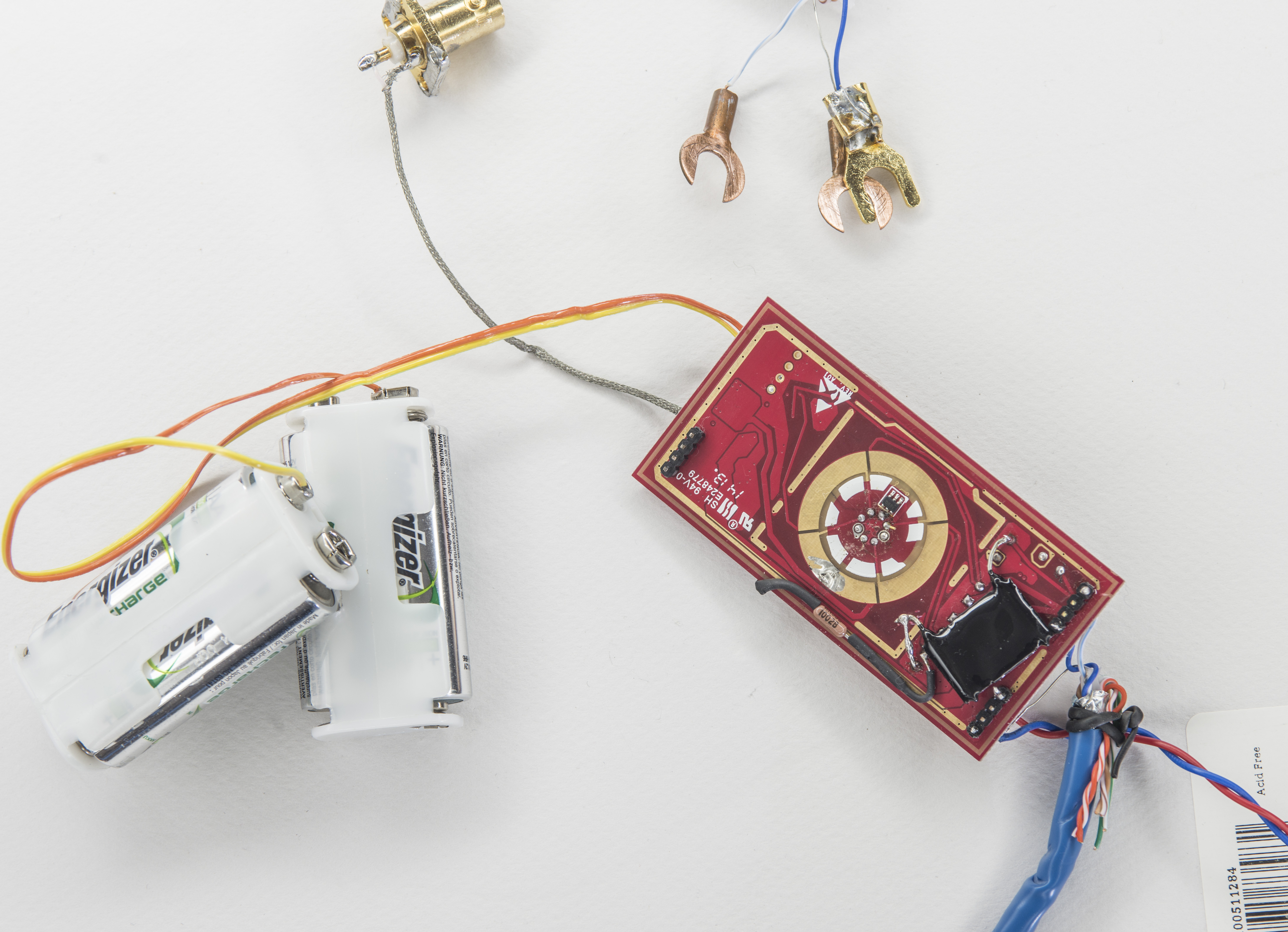
Image 33,34: Module #3 test setup with 10Ω wire-wound resistor (black on bottom)
As a bonus, here is some test data log, captured by HP 3458A 8½-digit DMM using Keithley 7168 nanovolt scanner. Settings for capture were NPLC100, sample 8 references based on LTZ1000/LTZ1000A each 10 seconds. All points are average of 32.
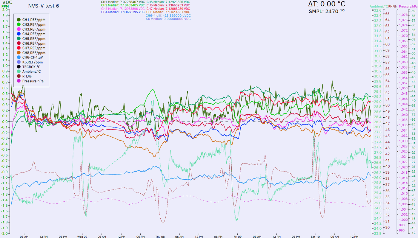
Image 35: 60-hour span over eight LTZ1000-based reference modules.
Linear LM399 low-cost version

Since not all applications would justify spending hundreds dollars for LTZ1000-based design, it’s often viable to use next second-best solution, with ovenized zener Linear LM399. This zener does not require lot of very expensive resistors and can be used in simple matter with stable current source.
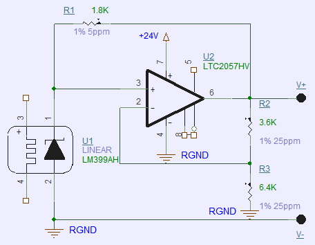
Schematics 4: xDevs.com Low-cost LM399 concept
This LM399-reference was not tested or tweaked for best performance.
Design provided as is, and apply your understanding as a priority.
It is NOT a finished ready to use project, unlike the LTZ1000 version!.
Simple bootstrapped voltage reference able to provide precise 10V (or any other voltage, depending on resistor values) almost independent of changes in power supply voltage, ambient temperature and output loading. Correct zener operating current of exactly 2mA is maintained by R1, a selected 5ppm/°C or better resistor, connected to the reference regulated output. Accuracy is primarily determined by three factors:
- Temperature coefficient of zener diode
- 1ppm/°C ratio tracking of R2 and R3 resistors
- Operational amplifier VOS offset errors.
The chopper amplifier LTC2057, with TCVOS of 0.015uV/°C, contributes only 0.0025ppm/°C of output error, thus effectively eliminating TCVOS as an error consideration.
Schematics for LM399-version reference in PDF-format
Schematics 4: xDevs.com Low-cost LM399 concept
Layout design of low-cost version

Image 36: xDevs.com Low-cost LM399 reference Rev.S00 top layer layout
Component locations

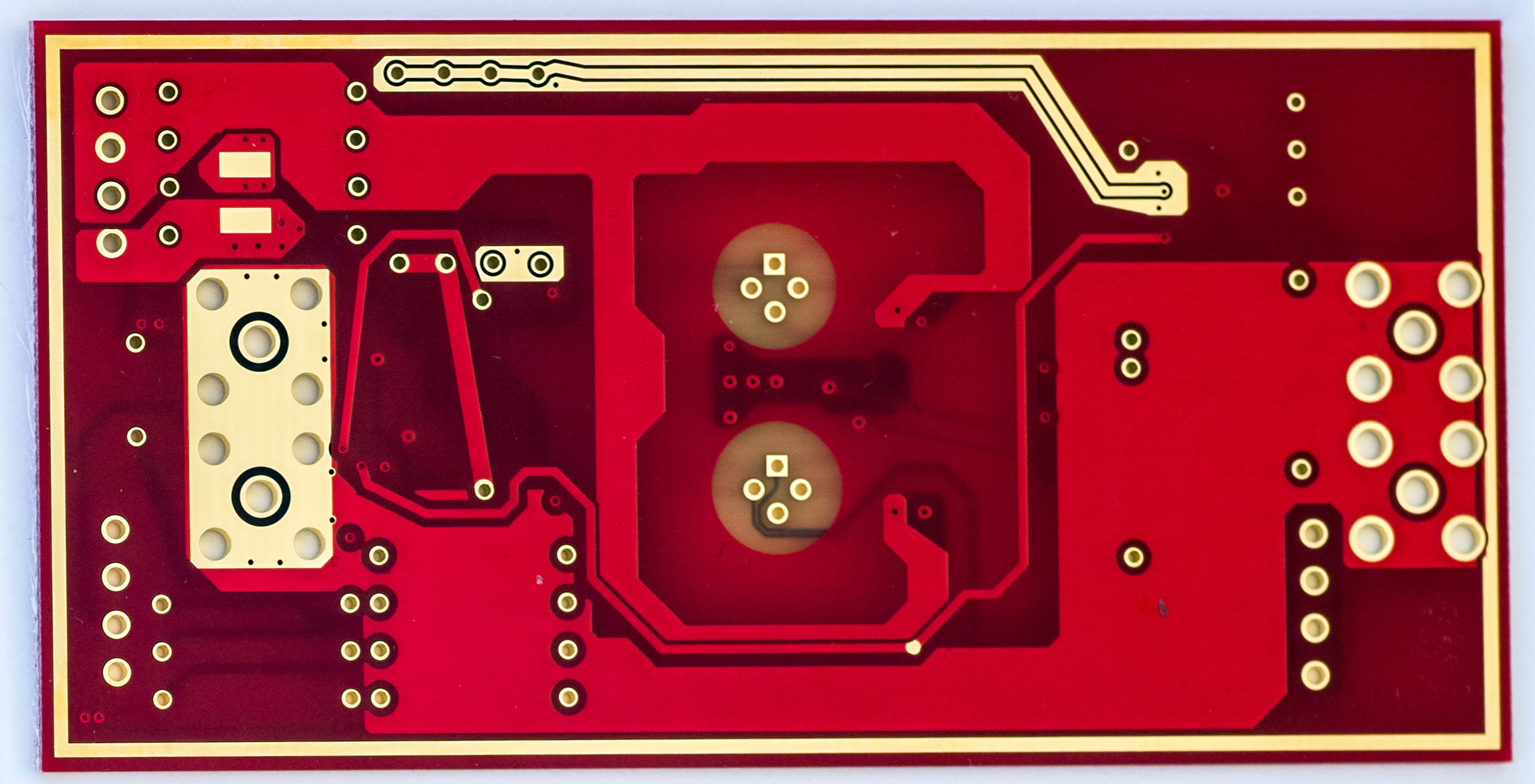
Image 37,38: xDevs.com KX low-cost voltage reference (Rev.S00) bare PCB, top and bottom side
Some tests of different LM399’s without heater power:
Gerbers for LM399-version
xDevs.com KX LM199/LM299/LM399 reference PCB GERBER RS274X, Rev.S02
RS274X Gerber archive is password protected, so you know what you doing before use. Password is https://xdevs.com/article/kx-ref/ just to make sure you read this article. PCB size is 3177 × 1575 mils, 4-layer on FR4 dielectric, with 55 ±5 mils thickness.
Stackup Z-heights used are shown in this PDF. Output units are INCHES.
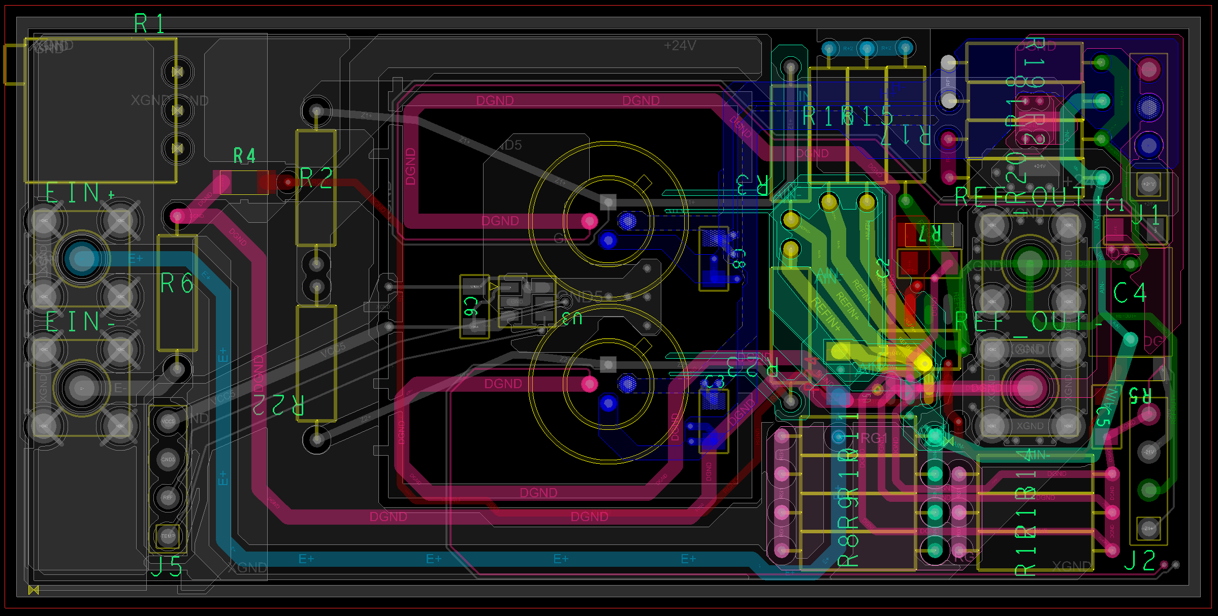
Image 39: xDevs.com Low-cost LM399 reference updated Rev.S02 top layer layout
This PCBA also available at OSH Park as free open-hardware project, if you want to order PCB directly from the fab house.
If you interested in this project build or have any questions, feel free to jump in comments. We also have article about special built LTZ1000-based KX reference and some aspects of test and verifications here, in separate article. Make sure to check it out.
Modified: Nov. 19, 2022, 6:50 p.m.
References
- Daniel Borrero Echeverry, A Low-Noise Current Supply for an Electron Electric Dipole Moment Experiment
- Interactive LTZ1000 calculator
- Lee, Mitchell. Application Note 82: Understading and Applying Voltage References.
- LT : LTZ1000 - Ultra Precision Reference
- EEVBlog : Forum for DIY calibrator project
- HyperPhysics : Page about standard volt
- Symmetric Research LM399-based reference manual
- J. Spreadbury, "The ultra-Zener... a portable replacement for the Weston Cell?", Meas. Sci. Technol., vol. 1, no. 8, pp. 687, 1990
- Tale 1 : Little jumper, or sharks in voltage references world
- An introduction to the New SI., Sandra Knotts, Peter J. Mohr, William D. Phillips
- OSH Park : Order Rev.B03 KX LTZ1000 PCB samples
- FeedbackLoop's YT Video on using KX REF.
- OSHPark : LM399 Rev.S02 version open-source PCB to order
- What’s All This LTZ1000 Stuff, Anyway?
- R3PAV : LM399AH DIY reference