Contents
Intro
Datron 4910 series include primary 4-cell SSR DC voltage standard and stripped 4911 (w/o 1V/1.018V divider) and 4912 (single cell only). These 4910 DC reference standards were one of the first replacements to the fragile and sensitive Weston cells. It provides stable 10 DC Volt output with a stability of better than 1 ppm per year. The unit features internal battery pack with long life and is great option for transfer applications and metrology use. In addition to the 10 V output, the unit also offers divided 1 V and 1.018 V outputs. Accuracy resolution of this standard is between 0.1 – 0.2 ppm. The operating temperature range is specified at 0°C to +40°C. Temperature coefficient of a 10 V averaged output and cell is 0.05 ppm/°C.
Datron 4910 with it’s 4 separate isolated cells, each of which have own reference is a direct competition to Fluke’s 734A reference system, which consist of four more modern Fluke 732B modules. Since 4910 was designed earlier prior to Fluke acquired company’s assets, it’s likely that 734A was developed after 4910 idea.
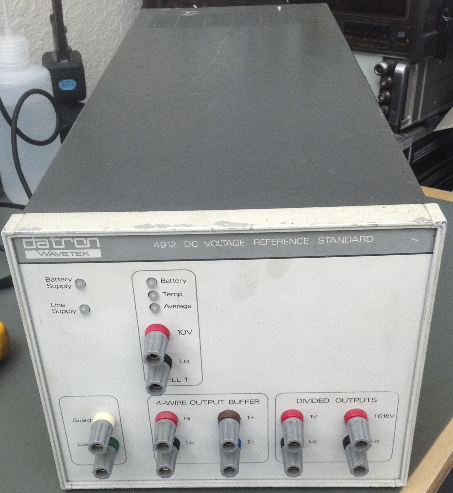
This time we will take a look on Model 4912, which is a member of the 4910 family series of voltage references from Datron/Wavetek. They are of a similar size and weight to the Fluke 732A and were in direct competition.
Fluke used their own Motorola-designed reference amplifier (SZA263) that found itself in many of Fluke’s products from DMM’s, calibrators, and voltage references. Datron went a different route here. They chose a commercially available voltage reference, the Linear LTZ1000. This LTZ1000 chip is considered as the best available buried zener reference by many engineers and the specifications of the 4910 series also show how competitive it is.
Datron/Wavetek references also made it into their other high end test equipment. They can be found in the 1271/1281 DMM’s, the 4920 AVMS, and in their multifunction calibrators like the 4708 and later Fluke’s own 8508A DMM. It was a departure from Datron’s older original designs where they chose several zener diodes and matched their tempco to provide a reference that was stable with both time and temperature.
The 4912 differs from the 4910/4911 due to its single “cell” output. The other two models include four “cell” outputs with the capability to average them together or connect them in series for up to 40V. The 4910 also includes a low impedance 4-wire output plus divided outputs at 1V and 1.018V.
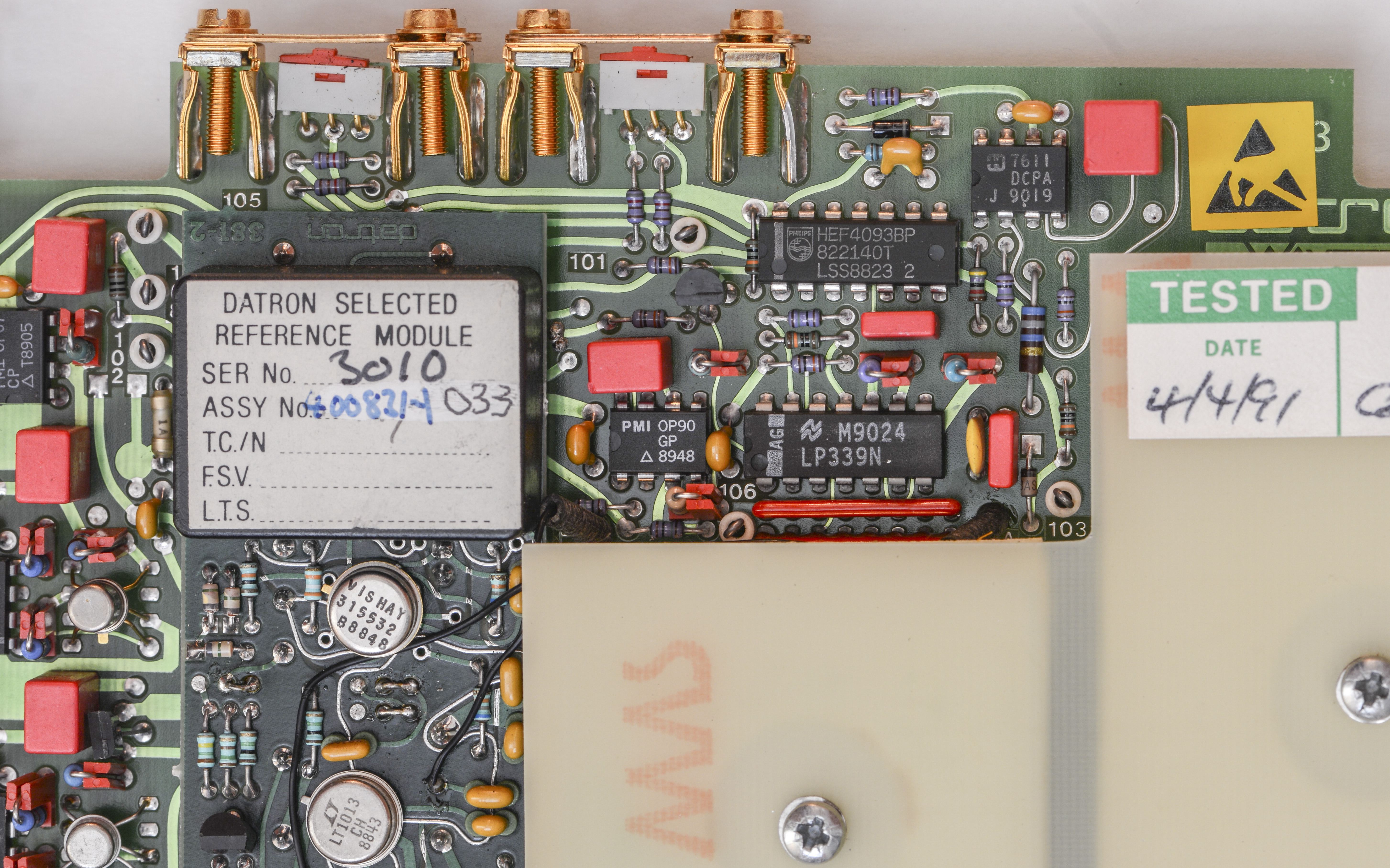
There is no manual currently available for the 4912 so the 4910/4911 manual was used for troubleshooting. This specific Datron 4912 was acquired from a member of the volt-nuts group as being defective, but in good physical shape. The condition in which it was received showed that there was an issue with the batteries/charger and the output was low at approximately 0.5 VDC.
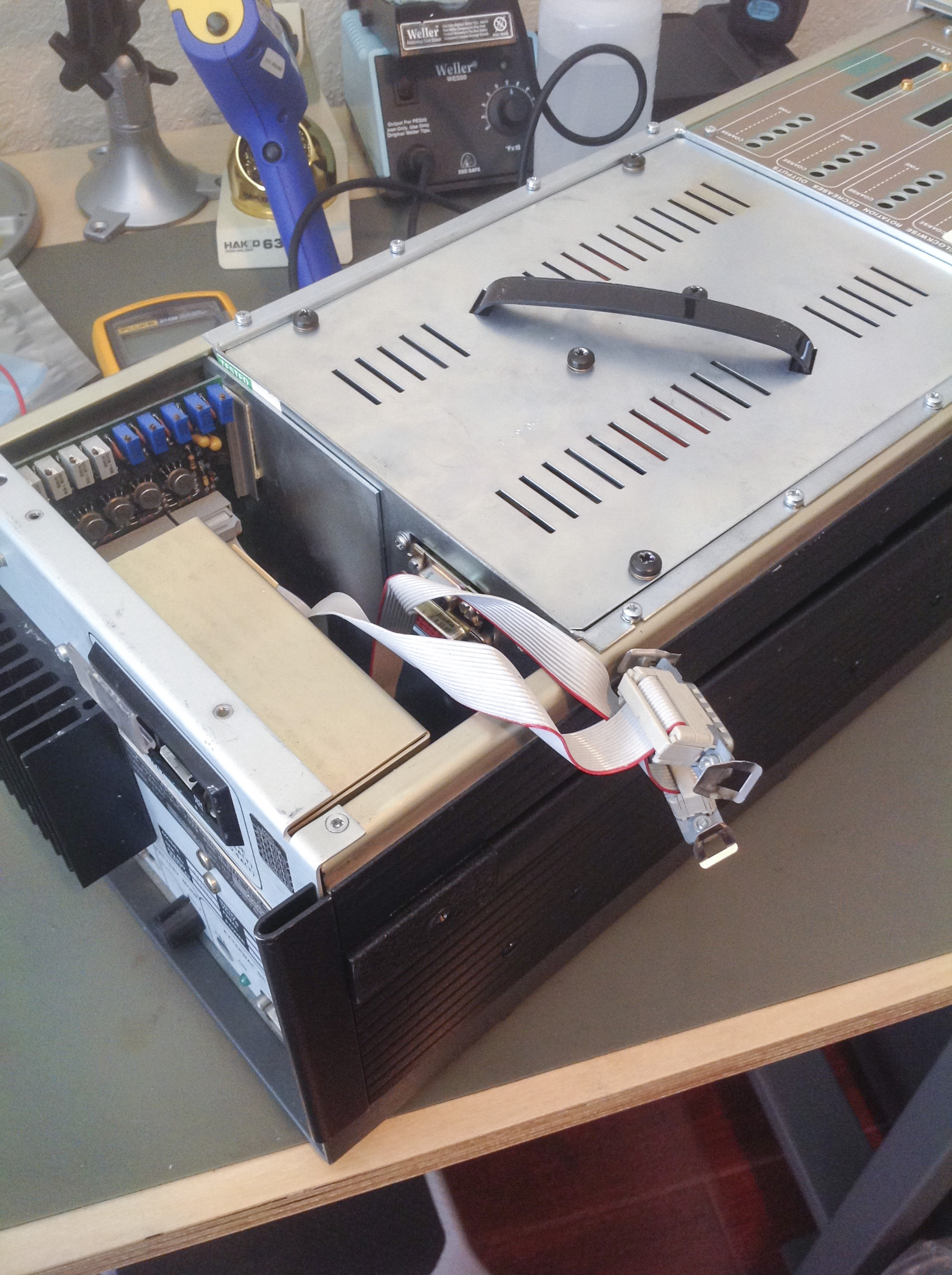
The unit was opened and inspected for obvious issues. Apart from a cable from the battery assembly being disconnected, there was nothing that appeared wrong visually. Time for disassemble and tests.
Teardown
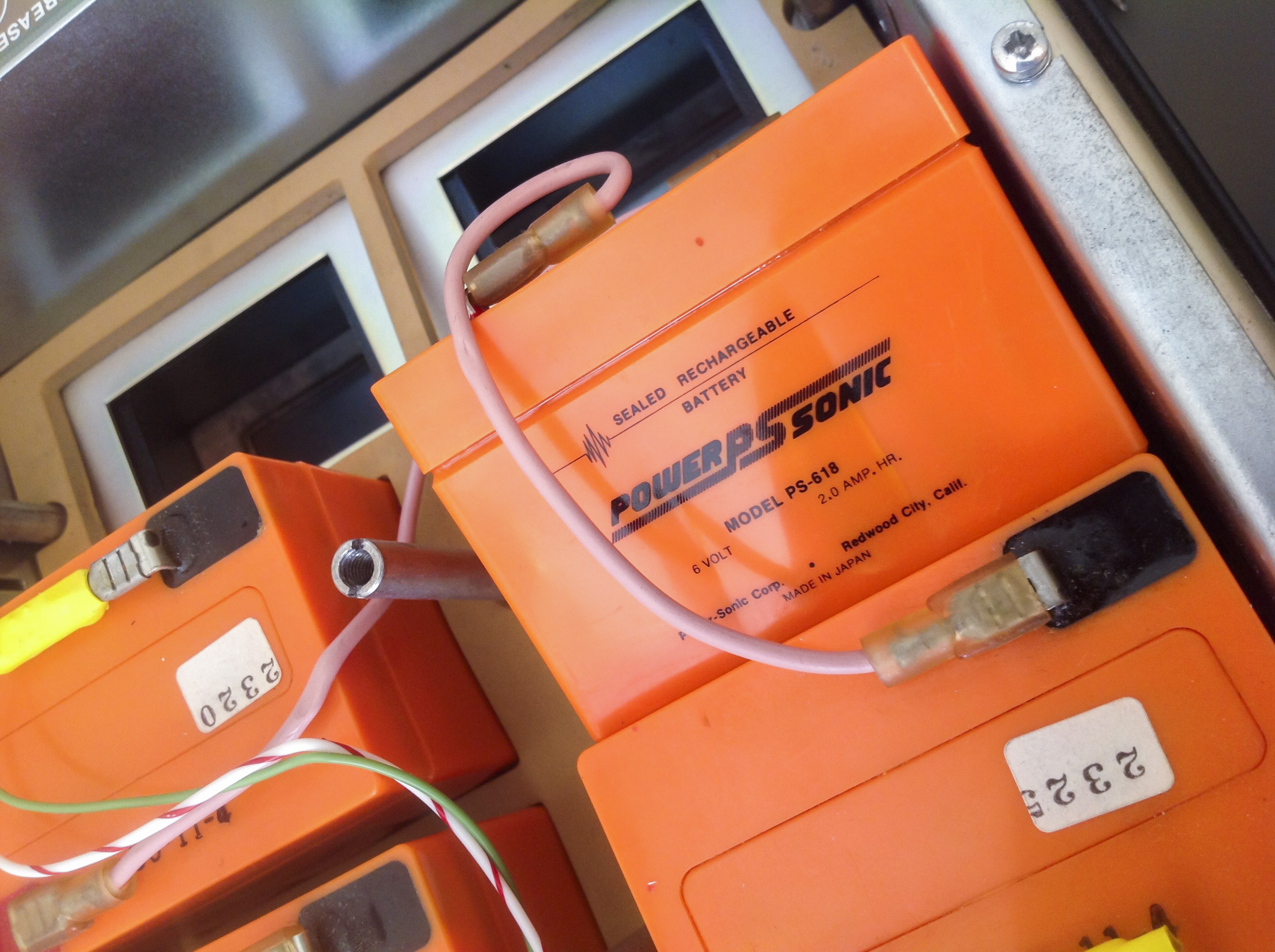
Battery compartment:
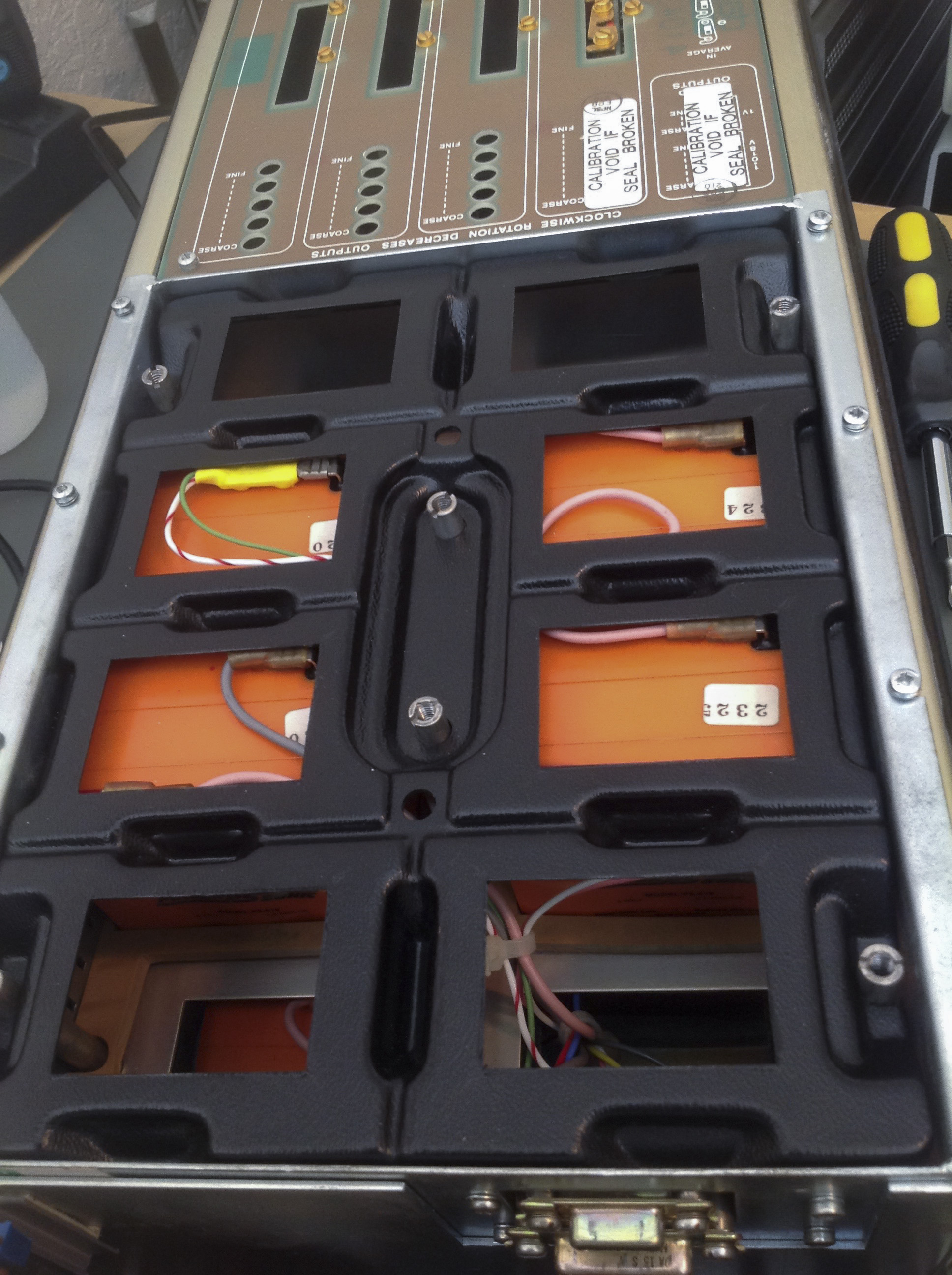
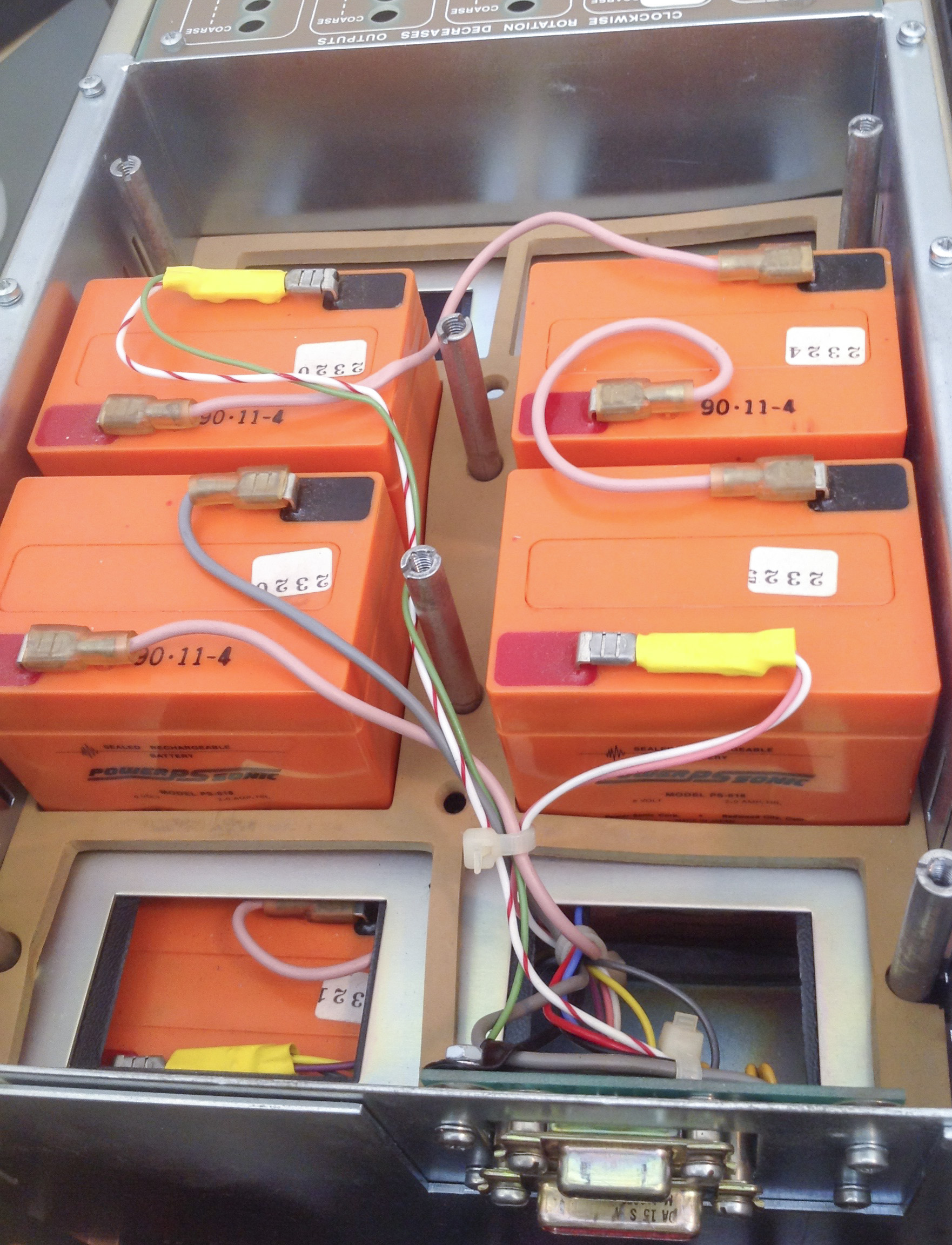
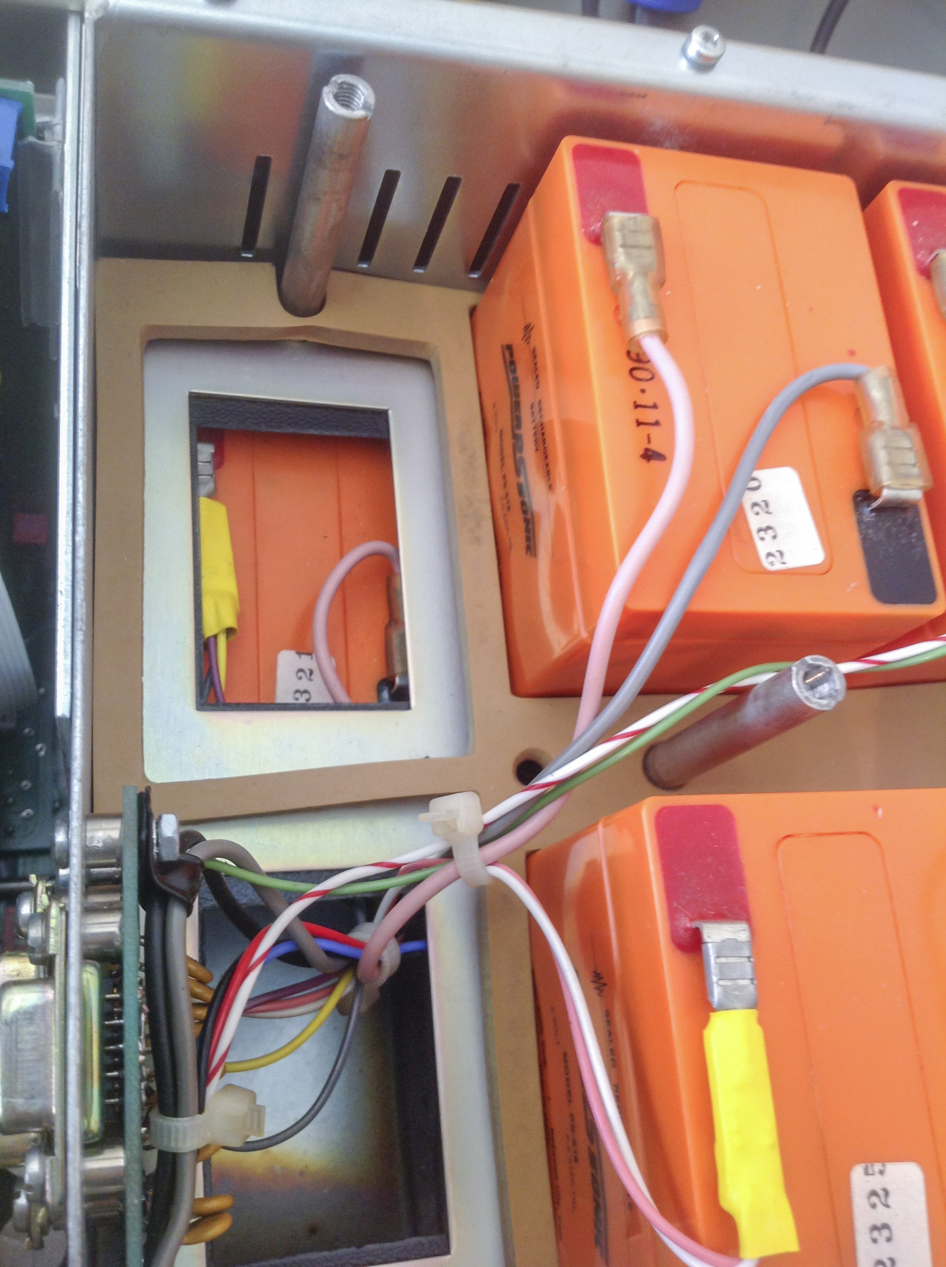
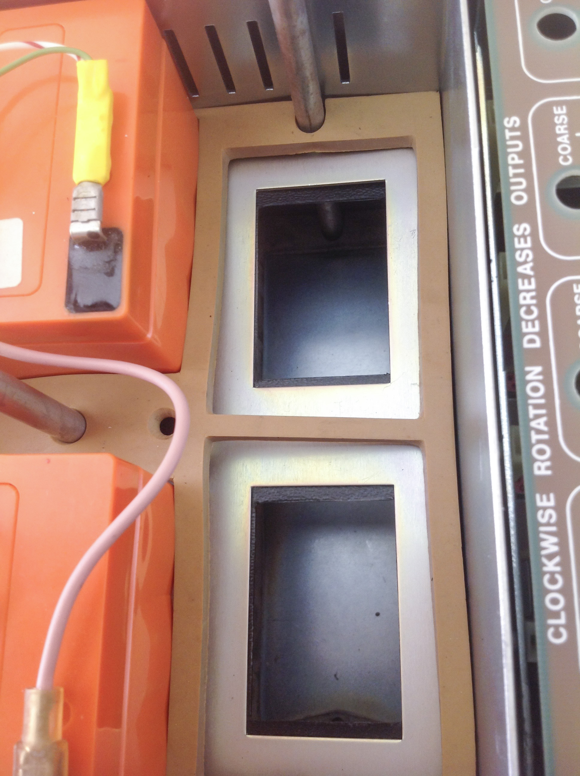
Used battery:
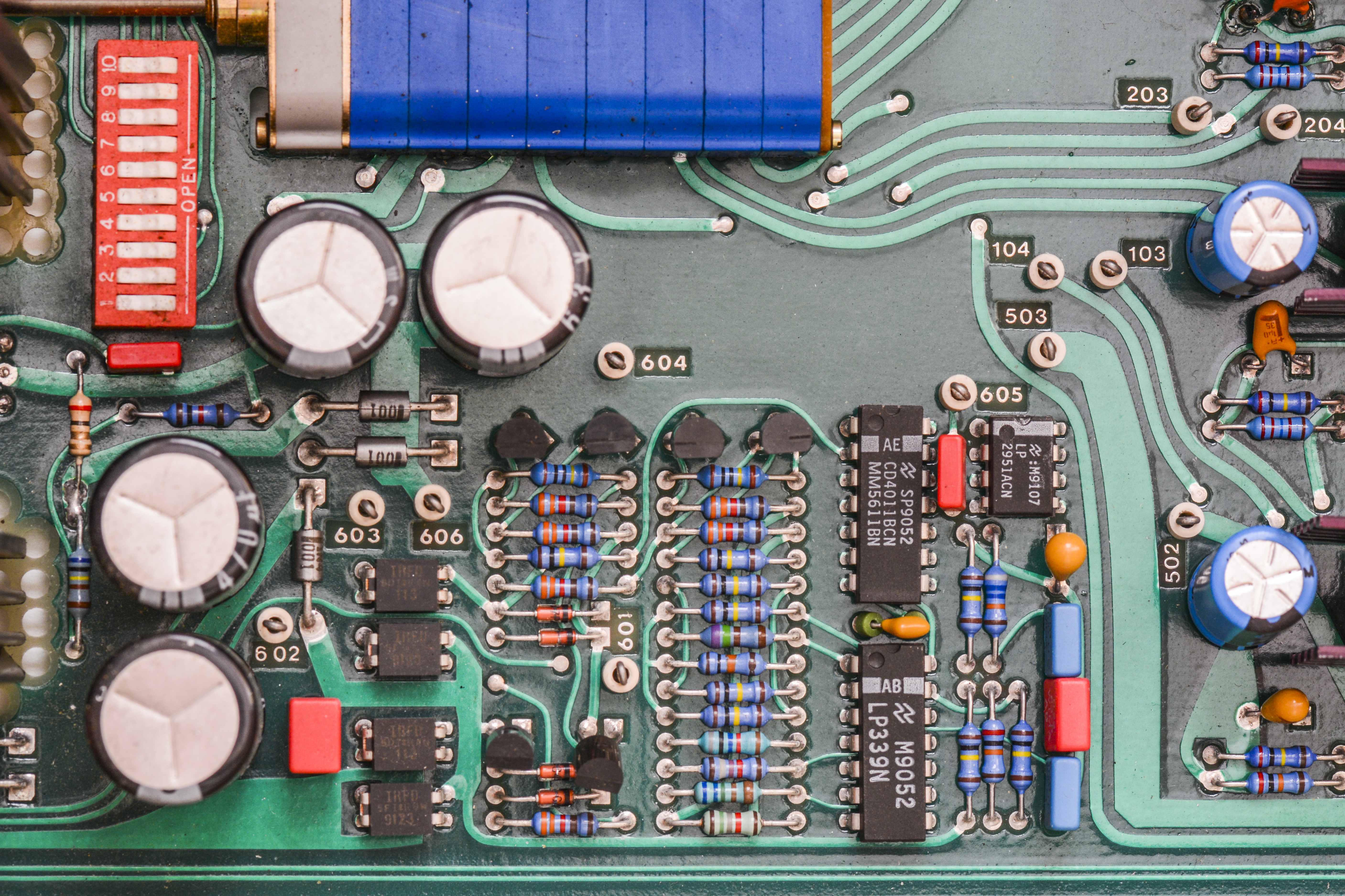
Power Supply Assembly
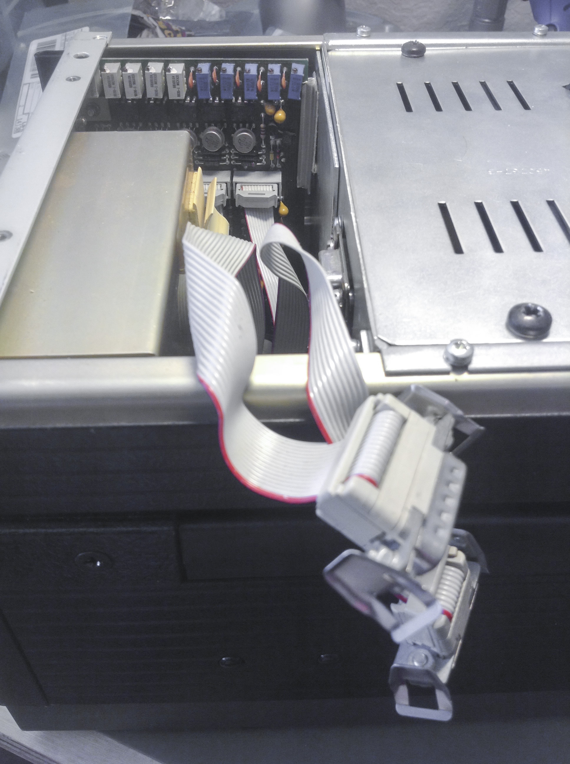
The power supply is part of the rear cover. It includes the transformer, power supply pcb, an external DC input connector, and a power input module. The power supply pcb has five identical isolated supplies.
It was easier to troubleshoot by comparing outputs of each of the regulators. Two of the regulators had a low input voltage. The circuits were traced out but no issue was found with the parts on the board. It was determined that the ground path in the two circuits was interrupted. The 1N4148 diode in the path on the ground side was removed and tested to be good using a Peak DCA75 on both supplies. A diode from one of the other supplies was removed for comparison and it was discovered that it was a 10V zener. Somehow the diodes were changed and the wrong type was installed. After replacing both diodes, the two supplies sprang to life and all looked well.
Further testing of the 10V output still showed no change in the output level. More troubleshooting was needed.
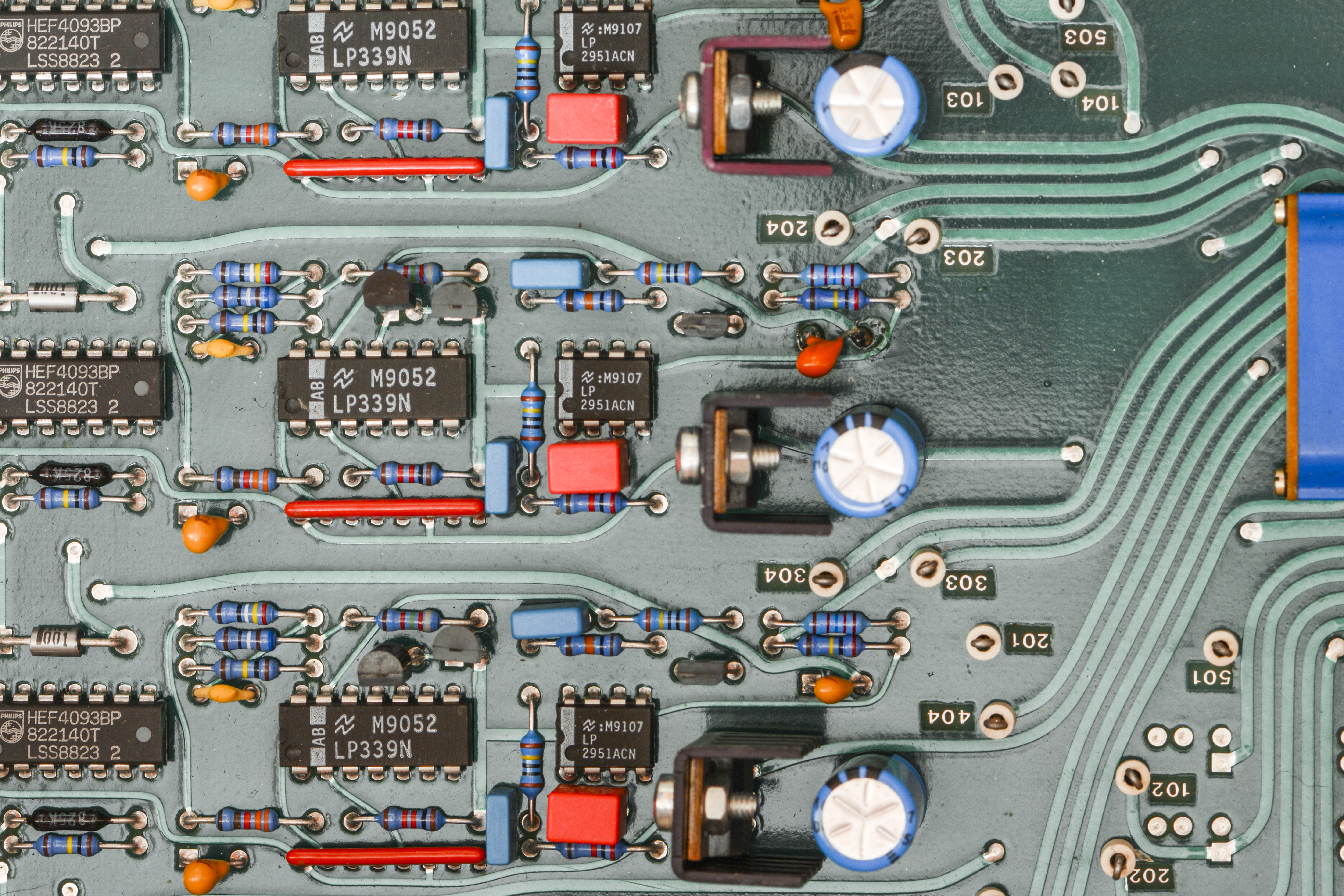
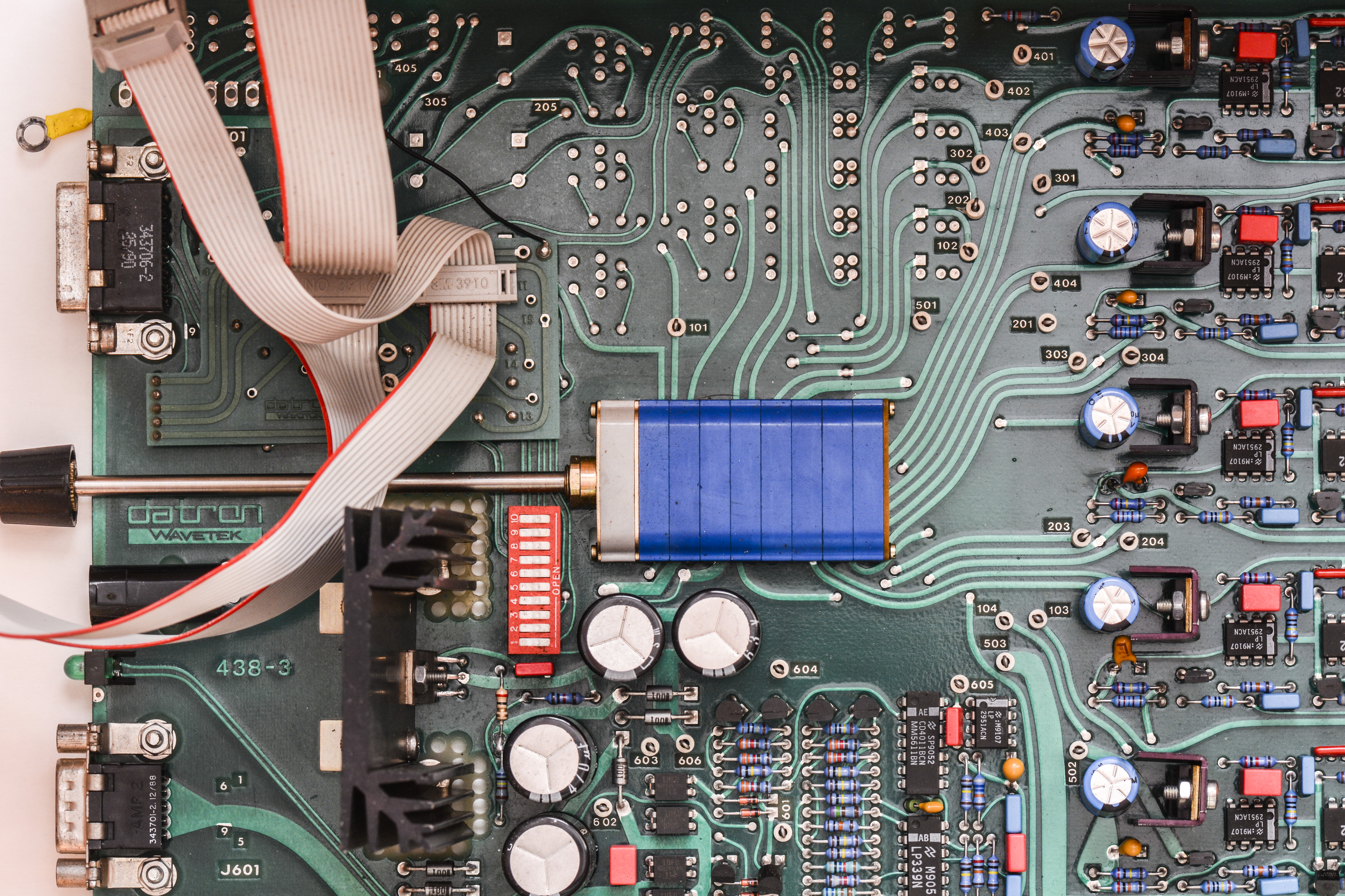
Main Board Assembly
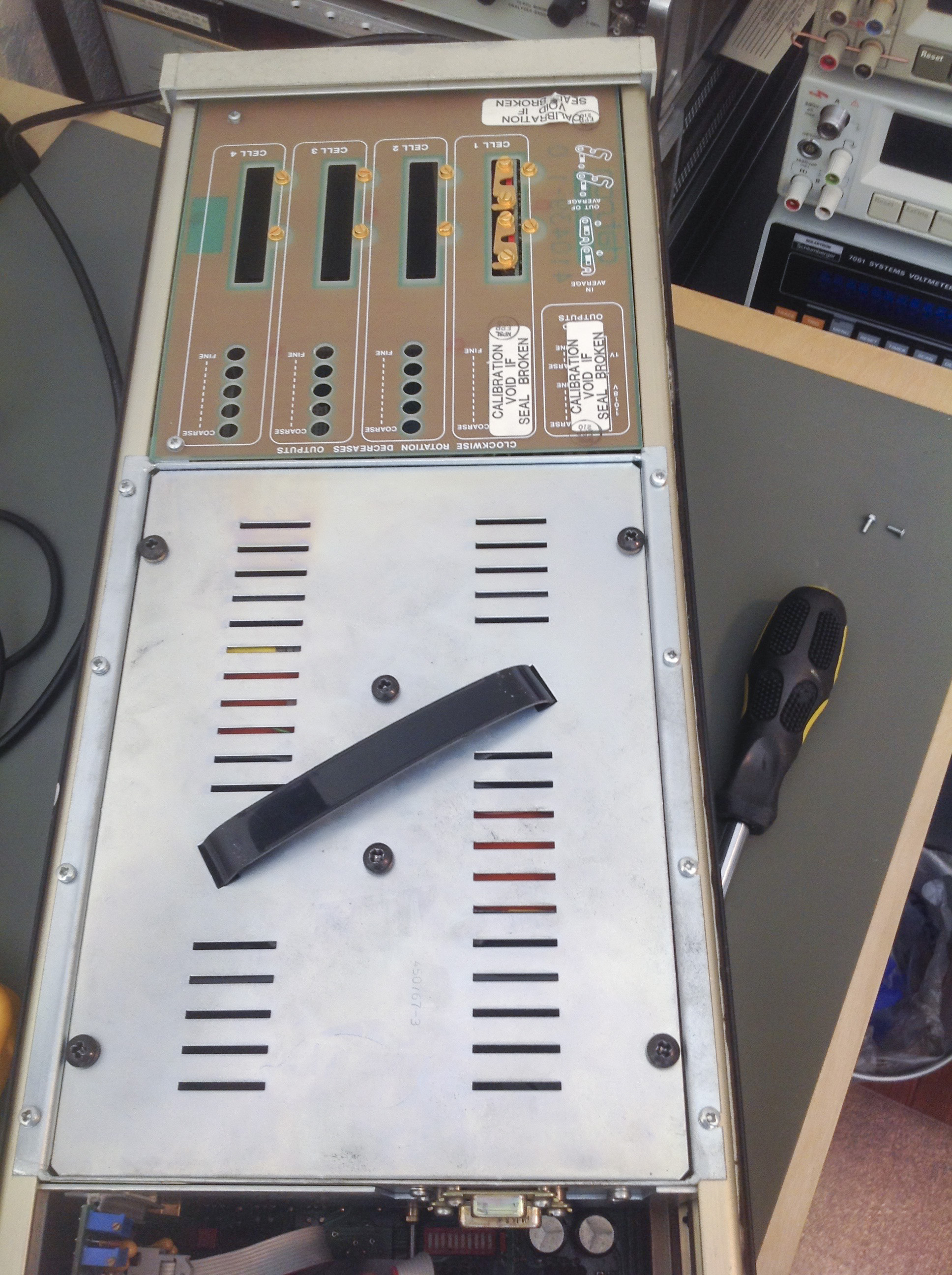
The main board includes separate circuits for each of the five supplies from the power supply assembly. This too made it easy to test. There is also a circuit to handle an external DC supply with its own regulator. A transit mode switch is also located on the board. The switch is used to select a low power mode for shipping of the reference. The switch protrudes from the rear cover. There are also connectors for up to four cell PCBs. It appears that Datron used the same backplane design for all three models. In the 4912 there are three slots that are not populated.
Comparing the voltages on each of the five circuits, it was found that the 12V was missing from two of three unused supplies. They have probably been defective for a long time but they had no effect on the operation of the single cell. The two supplies still needed to be repaired. The inputs were tested and found to be low. Measuring the resistance across the input path found that the two inputs were shorted to their respective grounds. There is a 1µF/35V tantalum on the inputs. They were removed and confirmed to be shorted. A temporary replacement was installed and the supplies were retested as having good outputs.
Again, the reference output was tested but the output was still at 0.5 V. Off to the cell PCB…
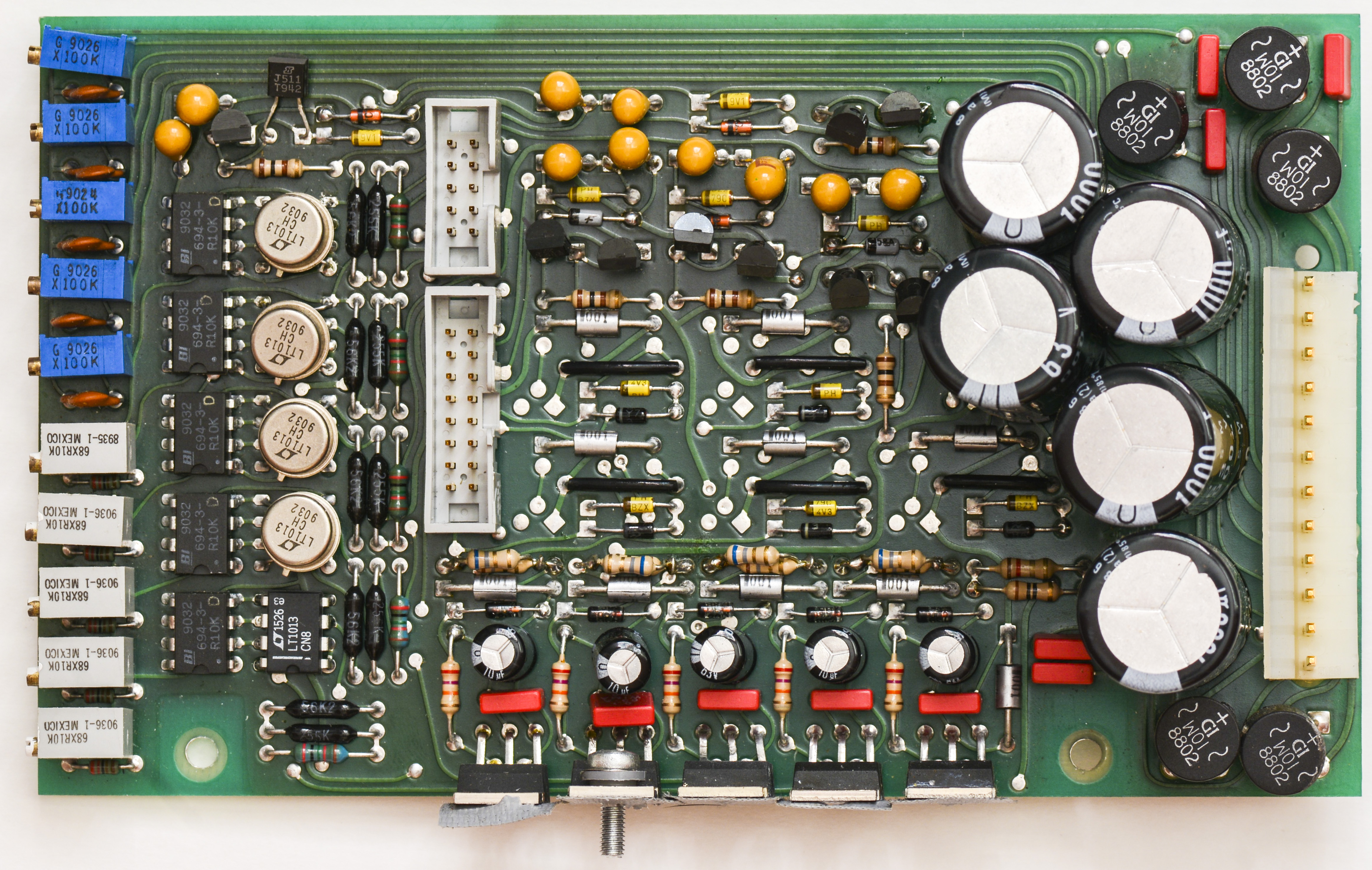
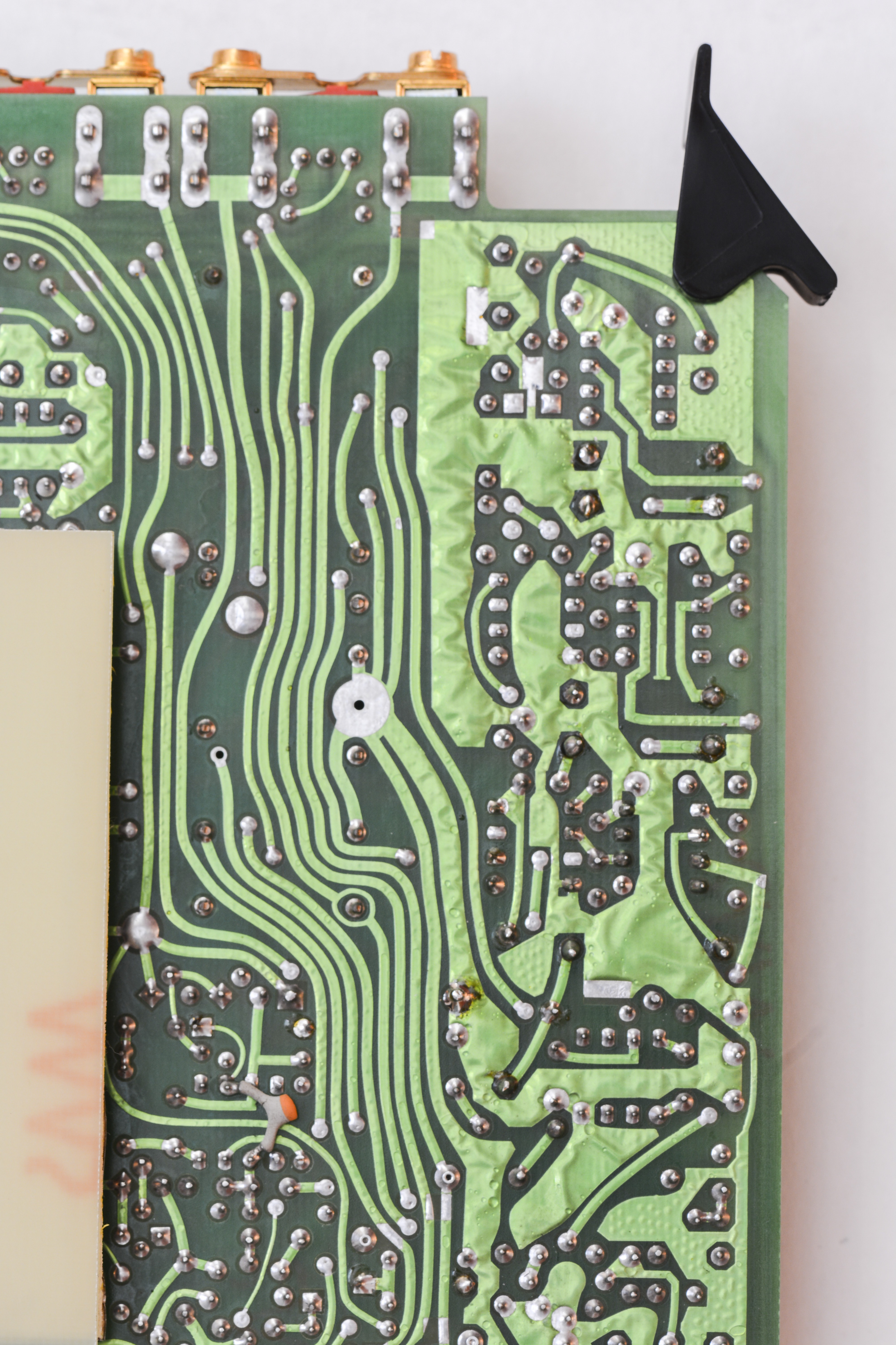
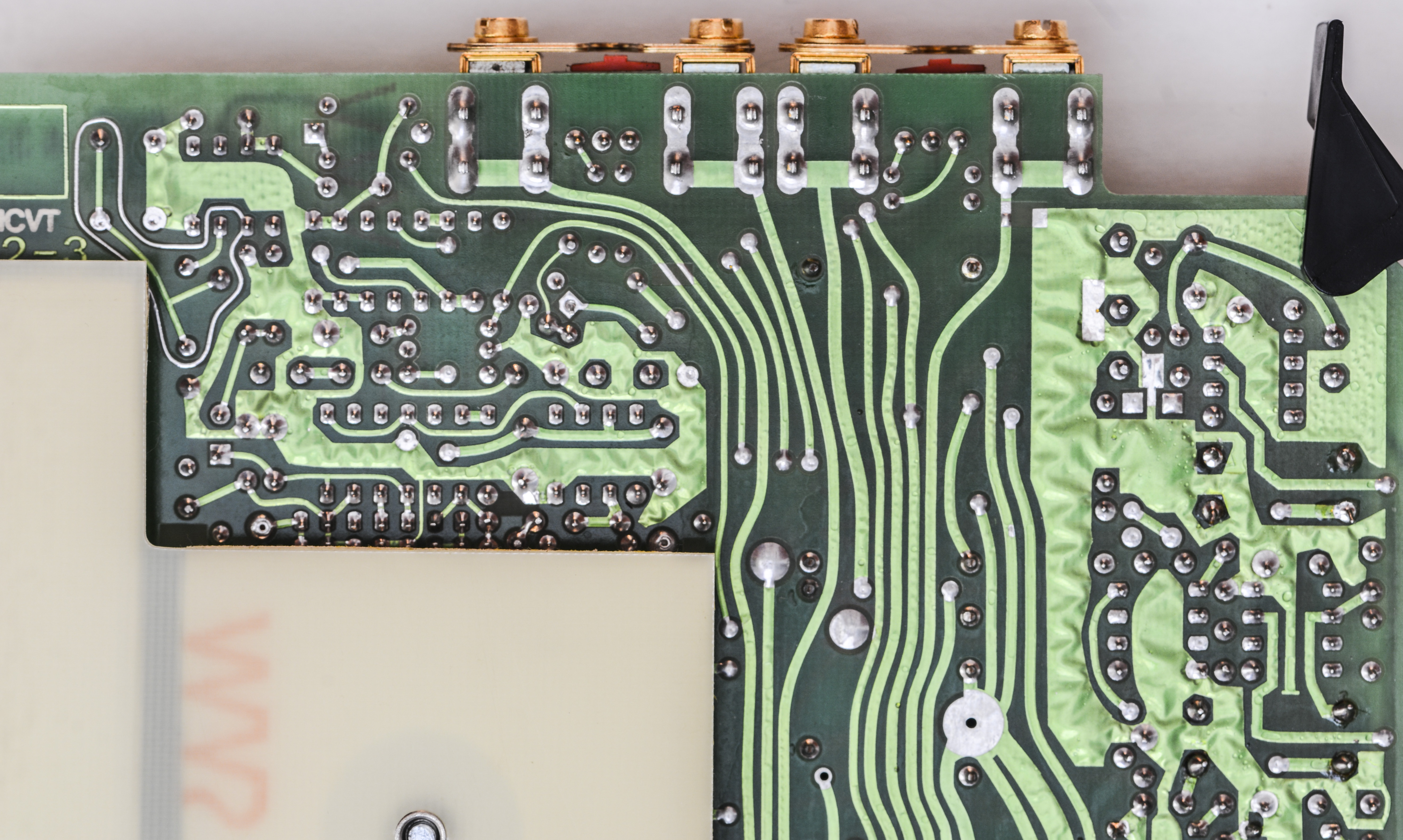
Cell PCB Assembly
The cell pcb contains the LTZ1000 daughterboard assembly and also the PWM divider circuits. The divider is broken into a most significant switch and a least significant switch of 16-bits and 8-bits.

The output of the LTZ board measured at ~7.23V between TP105 and TP108. This meant the problem was most likely in the output divider or op-amps. The HI and LO side of the output splits into both the direct output and averaged output. The continuity between the LTZ board LO out and the front panel LO was confirmed as good. The two jumpers connecting the averaged outputs were disconnected for testing purposes.
The LTZ board HI side output goes through two separate op-amps. It was difficult to confirm whether U109 was working as its output was low (0.5V). U111’s output was ~11.5V but the output at the front panel was missing. The resistance between the HI and LO outputs at the front panel measured 7 ohms. It was suspected that more bad capacitors would be found.
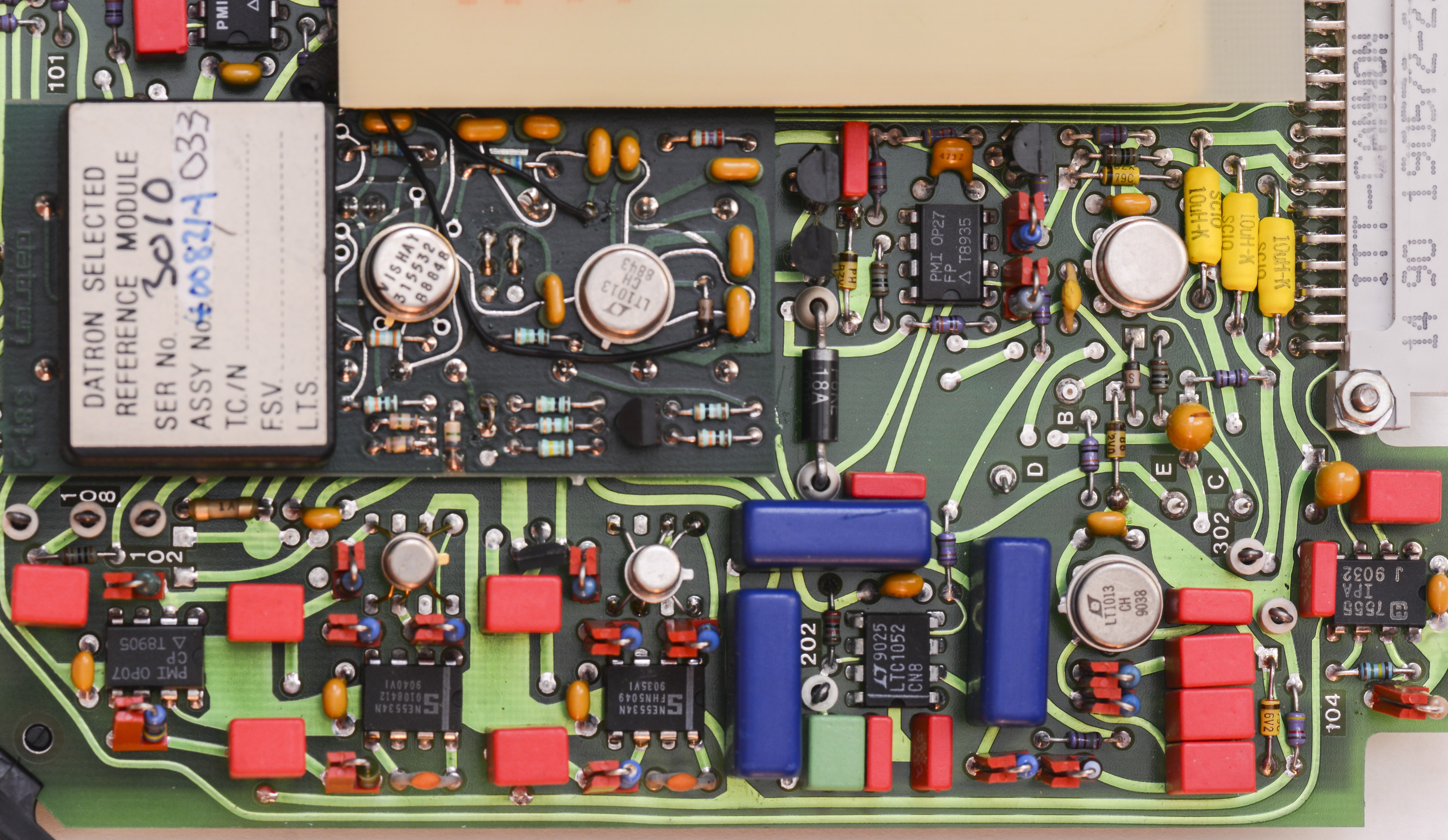
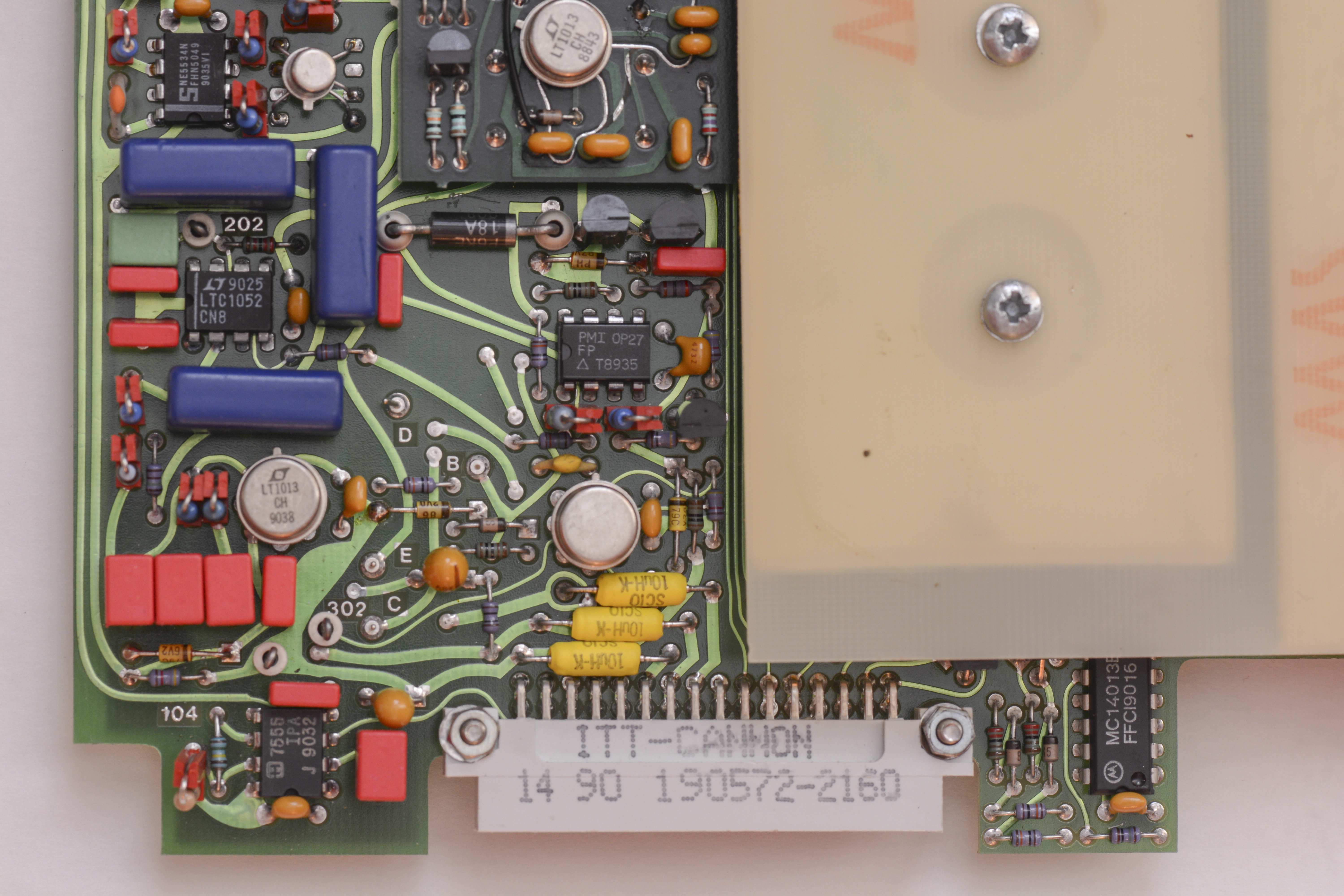
All capacitors on the board were measured in circuit but only a couple were across the HI/LO outputs. They were removed and measured. Neither were found to be shorted. Probing around the board searching for shorts proved nothing. The 10V path goes into both dividers. The signal name is 10V(B) according to the schematics. All components in the two dividers were checked but the only issues found were two JFETs (Q204,Q206) had a low resistance across their terminals. They were removed from the pcb one at a time and tested on the DCA75. No readings appeared to be bad. Measuring resistance at the outputs showed that it was now ~130 ohms. The 10V output was then measured with the two transistors removed and it read 9.4V.
Q203,Q205, and Q208 were removed and tested with the DCA75. They also tested as good. It was decided that the transistors in this part of the board would be ordered. Q204 and Q206 have been marked by Datron so most likely they are binned parts. They could also be matched to each other. This will have to be tested if either one is determined to be defective.
To be continued….
Modified: April 24, 2016, 4:13 p.m.