Contents
- What is this about
- Disclaimer
- Introduction
- First look
- Documentation and manuals
- Diagnostics and repair log
- Modifications
- Calibration
- Results and performance
- Summary
What is this about
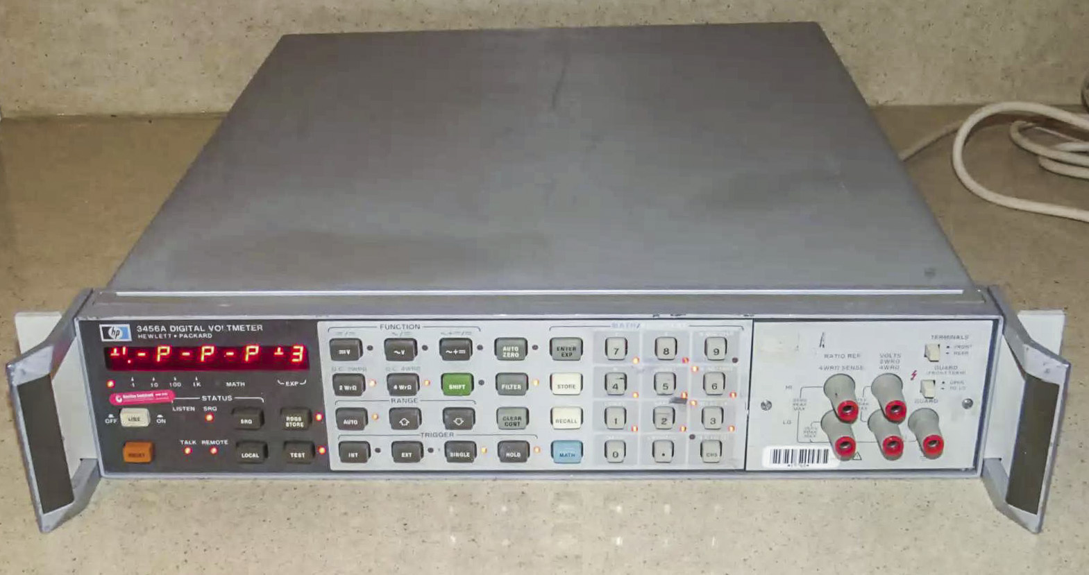
Repair work log and restoration project for Hewlett-Packard (later Agilent Technologies, now Keysight Technologies) Model 3456A 6½-decade system multimeter is covered in this article. Difficulty of this repair was in inability to run self-diagnostics and lack of reference working meter to trace issues. After repair there are some extra modifications described and tested, to gain performance improvement on this multimeter.
Disclaimer
Redistribution and use of this article or any images or files referenced in it, in source and binary forms, with or without modification, are permitted provided that the following conditions are met:
- Redistributions of article must retain the above copyright notice, this list of conditions, link to this page (/fix/hp3456a/) and the following disclaimer.
- Redistributions of files in binary form must reproduce the above copyright notice, this list of conditions, link to this page (/fix/hp3456a/), and the following disclaimer in the documentation and/or other materials provided with the distribution, for example Readme file.
All information posted here is hosted just for education purposes and provided AS IS. In no event shall the author, xDevs.com site, or any other 3rd party, including HP/Agilent/Keysight be liable for any special, direct, indirect, or consequential damages or any damages whatsoever resulting from loss of use, data or profits, whether in an action of contract, negligence or other tortuous action, arising out of or in connection with the use or performance of information published here.
If you willing to contribute or add your experience regarding HP/Agilent/Keysight instruments repairs or provide extra information, you can do so following these simple instructions
Introduction
Used multimeter and instruments manufactured by HP are well recognized and highly respected among hobbyists and engineers, who are maintaining and taking care of old, but still very functional instruments. One of such well-treated instruments are leading multimeters of their age, such as benchtop units HP 3455A, HP 3456A и HP 3457A. All these meters have 6½-decade resolution. First two models ,HP 3455A and HP 3456A sometimes can be found for very low prices on secondary markets, providing bargain entry into high-resolution gear for beginners and students.
But often such low-priced units have failures and issues, and likely require repairs and recalibration. So happen with me, when I could not resist to bought used HP 3456A on eBay for just $50 USD with condition in description as power on, further not tested. Worth to note, in 90’s these 3456A’s were selling for about $6400 USD. Time flies!
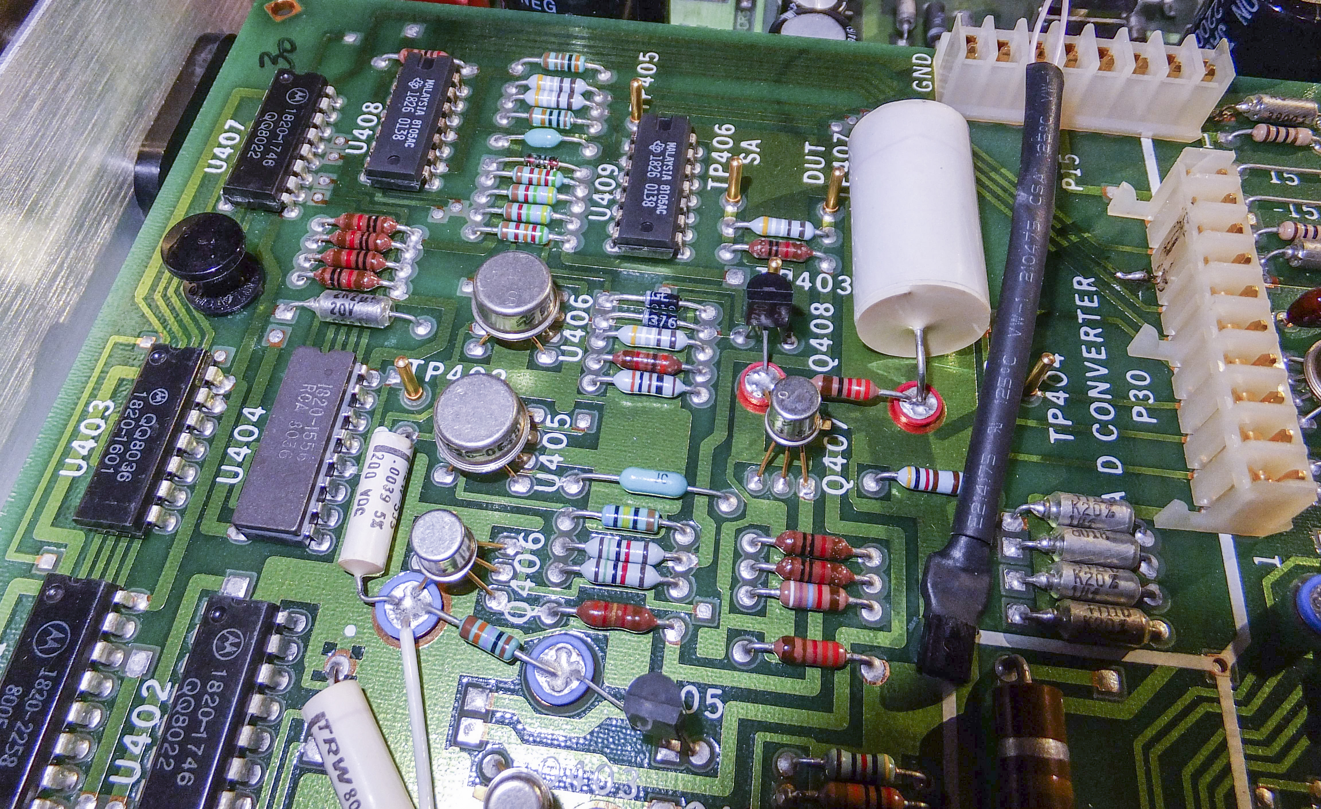
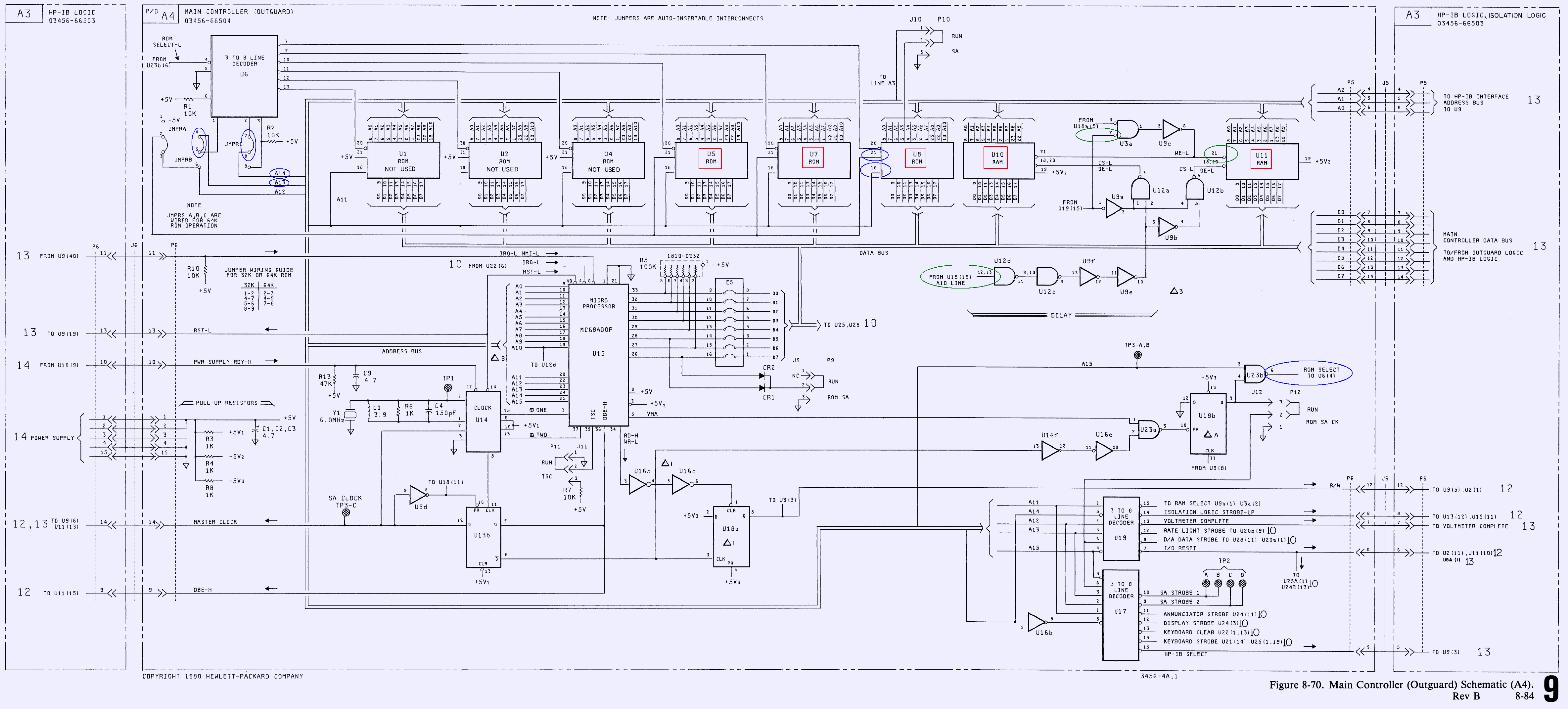
Detail architecture of instrument can be studied from block diagram, represented in operation manual.
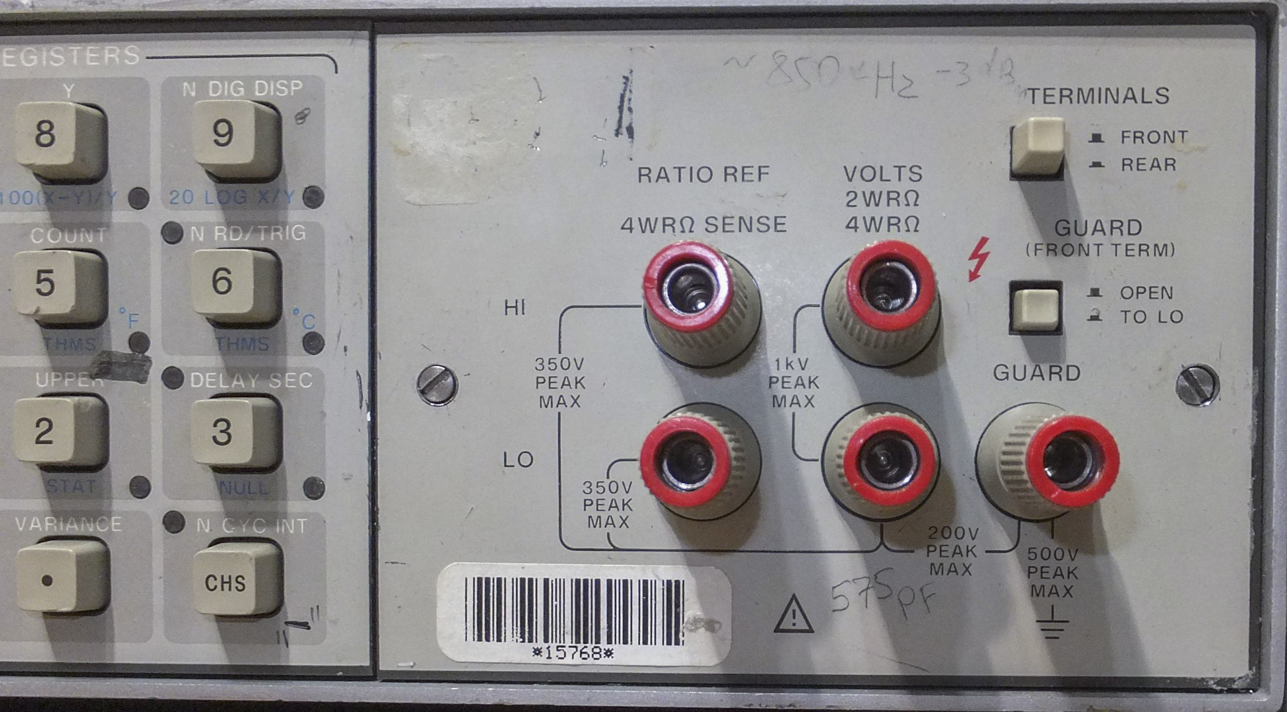
Depending on operation mode, input terminals are connected either to resistance measurement circuitry, or DC voltage attenuation/protection circuits or RMS AC voltage convertor, which is located on module А40. Later have own divider and amplifier and have separate measurement path for ADC. DC voltage circuitry also handles direct measurement or ratio measurement switching, amplification of low voltage ranges, such as 1 VDC and 0,1 VDC to 10 and 100 times accordingly, as well as using 100:1 divider for high-voltage measurements on 100 VDC and 1000 VDC ranges. There is also optional filtering circuits, which can be disabled. Resulting voltage, properly scaled for 10V range is later fed to integrating Multislope A/D convertor for further conversion of analog signal into digital code. Reference voltage around 6.9VDC for A/D convertor is generated by dedicated module with ovenized buried zener reference LM399.

All analog inguard domain, including switching and A/D conversion parts, are controlled by inguard-controller, which is called so due to location in guarded faraday cage, isolated from rest of chassis and mains circuitry.

This controller receiving commands of operation mode, (ACV, DCV, Ohm or RATIO measurement) and type of operation (such as autorange/manual range, integration time, resolution, autozero functions and filtering) via isolation transformers interface with main outguard processor/controller. This is interesting implementation, as modern instruments usually use optocouplers for similar isolation task.

Main outguard processor is also handing keyboard processing, display operation and math functions for received data, as well as provide digital interface to computer via GPIB. Power supply (PSU) is providing power for whole unit, with special care taken for separation between outguard and inguard domains, as these parts taking power from separate, isolated windings in transformer.
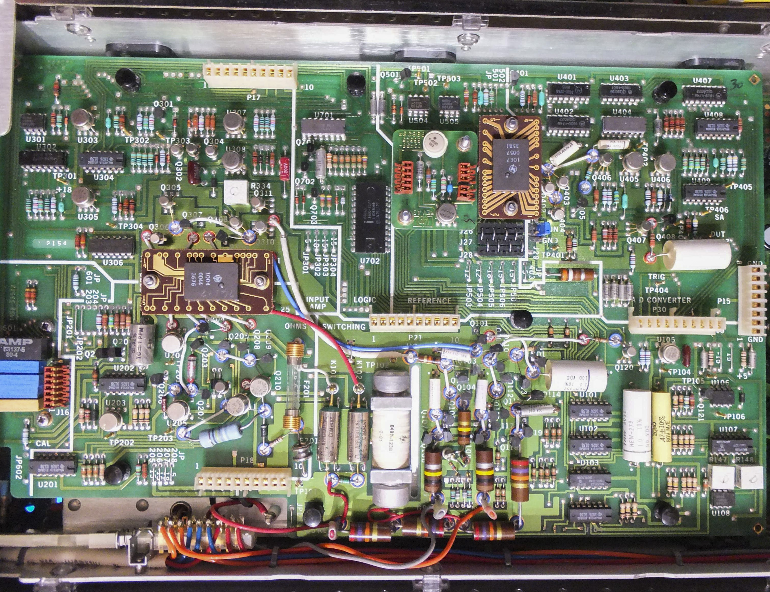
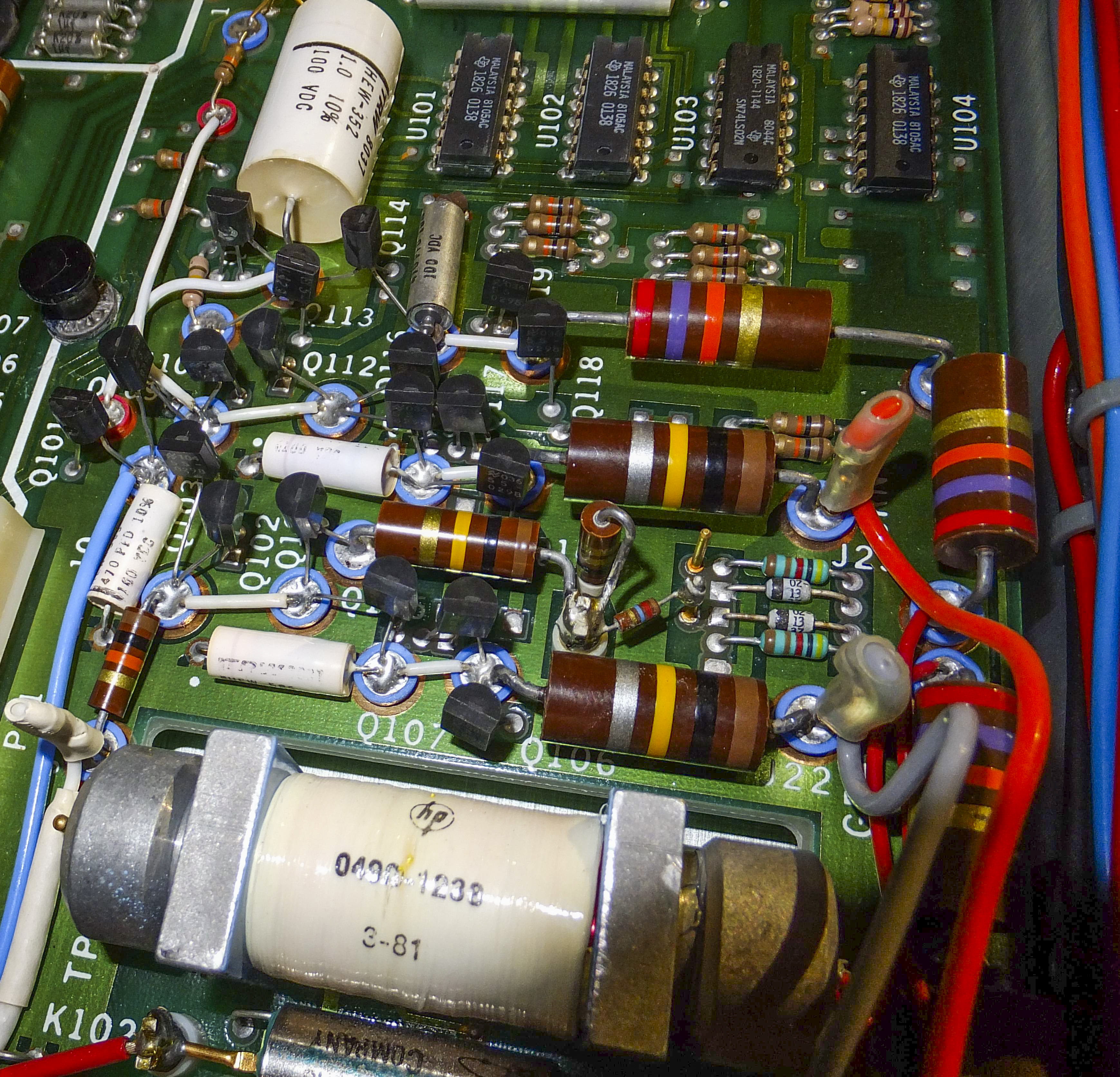


Analog circuitry domain implements various precision resistors and hybrids, which help to maintain high performance and stability of critical circuits.


First look
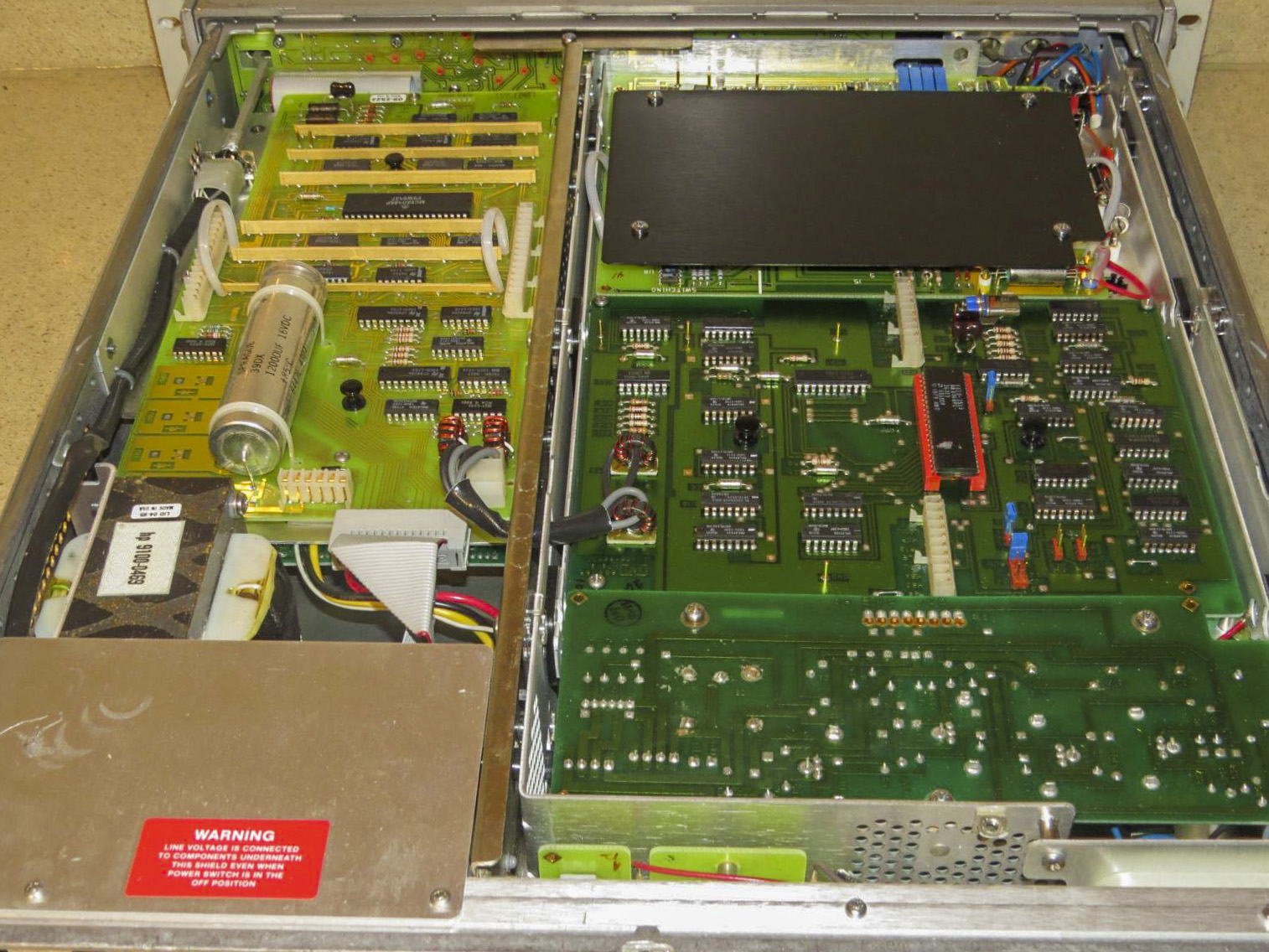
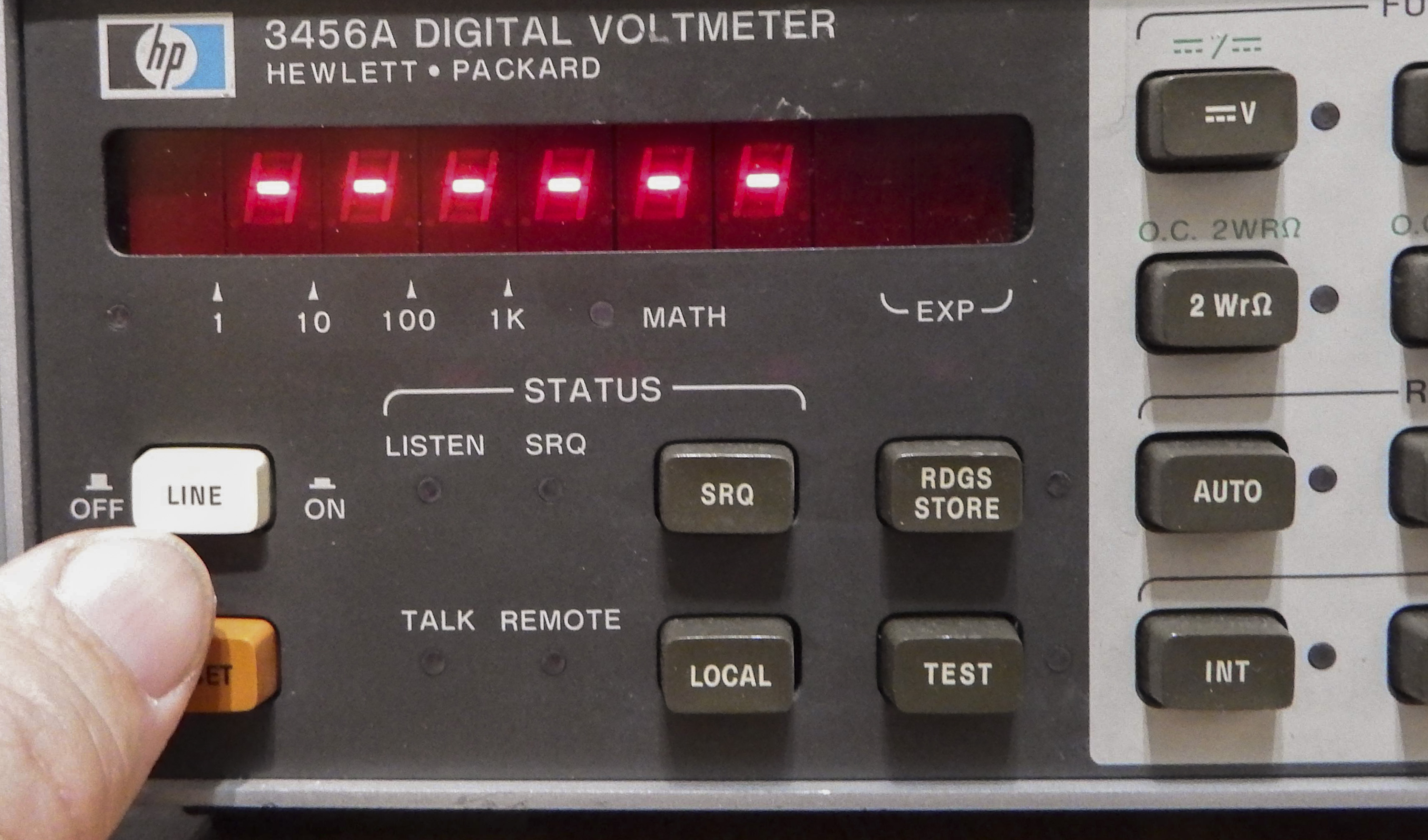
Just as honest description from seller, unit was missing one of outer covers and inguard internal shielding covers, and showing garbage on display and front panel LEDs:
After arrival unit was switched for proper mains voltage (220VAC here), prior to connecting power. First attempt to boot meter revealed random front panel operation, without any system or pattern. Most of keypresses do not change any behavior, and some cause random indication changes.
Sad fact, that running diagnostics with buttons «TEST» and «RESET» also impossible.
Documentation and manuals
HP 03456-90006 : 3456A Digital Voltmeter Operating and Service manual, Revision March 1, 1982
Better quality copy, part 1 and part 2
High-resolution copy of manual HP 03456-90004
Calibration procedure for HP Model 3456A
Catalog pages, covering HP 3456A
HP Service notes
HP Model 3456A service notes 03456-13A
HP Model 3456A service notes 03456-14A
HP Model 3456A service notes 03456-15B
Firmware
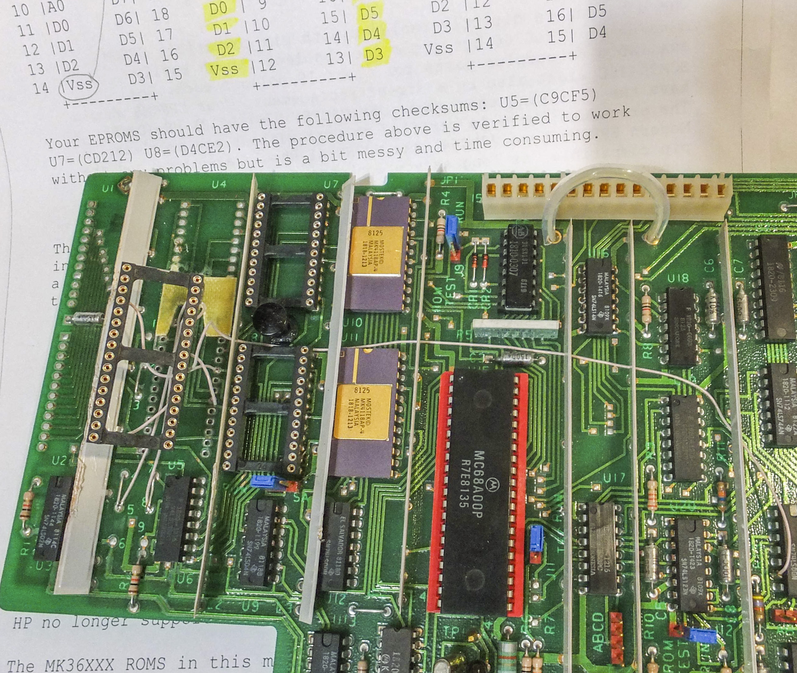
Firmware archive for ROM U7, TMS27PC256NL (TEXAS INSTRUMENTS), HP PART NO 03456-65501 D/C 9049 CHECKSUM 00469BE9. Binary file, 32 Kbytes.
Diagnostics and repair log
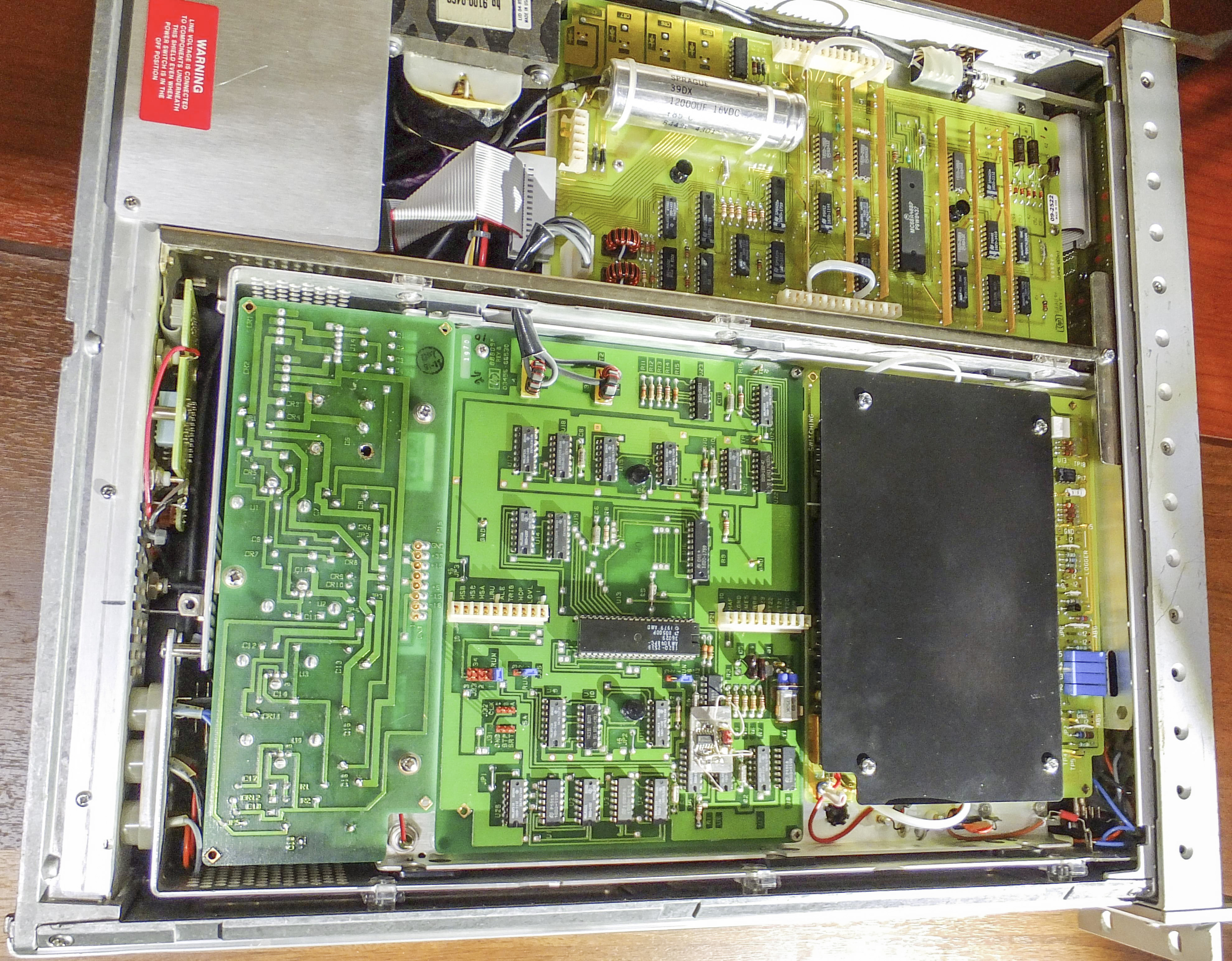
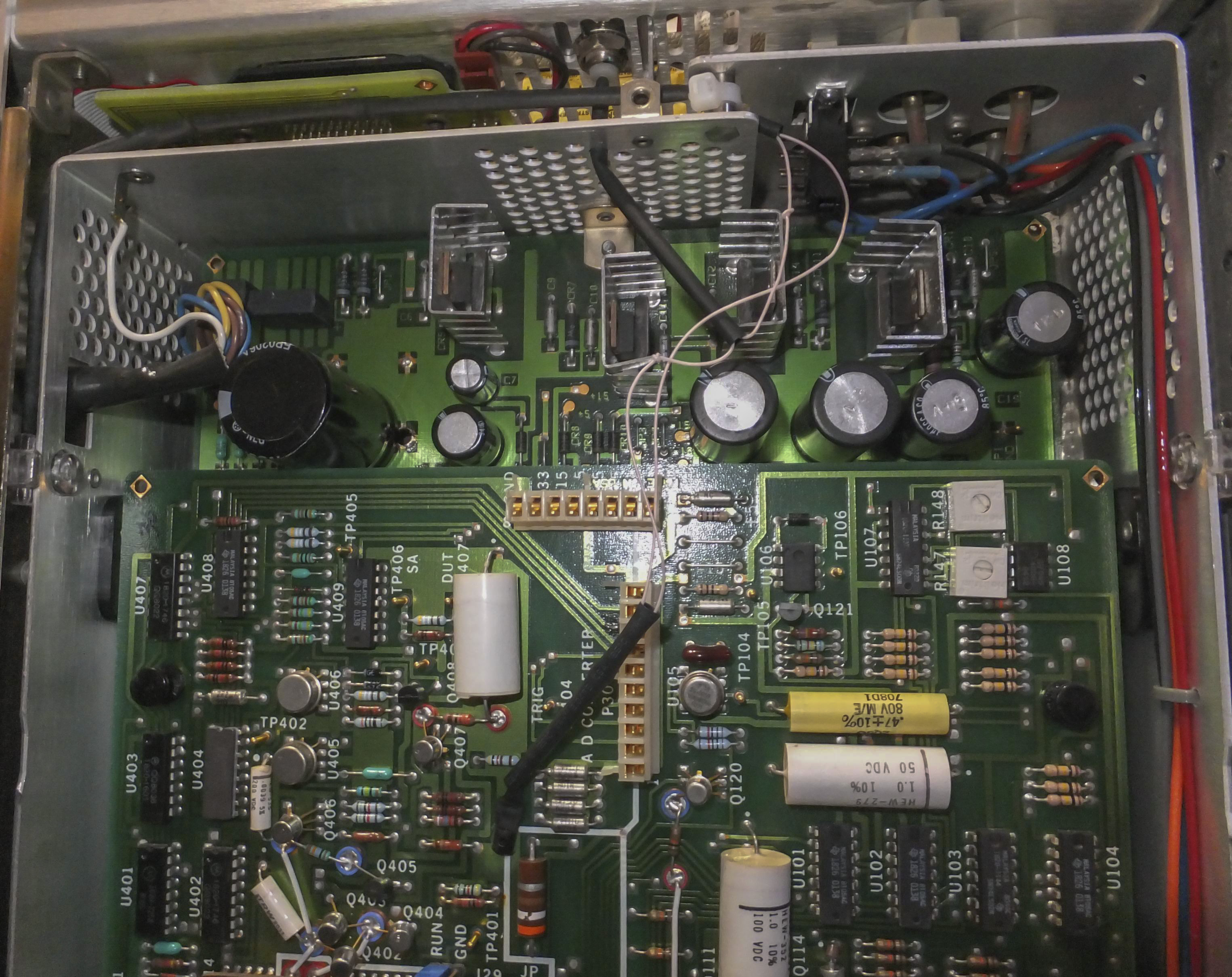
Visual inspection did not show any serious problems, so we started diagnostics and repair from power supply. It’s always a good start, as in old instruments power is often first point of failure, due to aged capacitors and faults in power components.
Here and later, all reference designators are shown according to schematics from manual 03456-90004, which we linked already in very high quality here.
Power supply repair
Power supply test revealed serious reduction of +33V rail output. Root cause of this was dried out old electrolytic capacitor C7, but all other electrolytic capacitors with capacity over 1µF were replaced as well. Usually not bad idea to install higher capacitance and voltage ones, if area and size permits.


С13 and С15 – 2200 µF 50…63 V instead of original 1000 µF;
С16 and С19 – each 1000 µF 50 V instead of 330 µF and 470 µF;
С5 – 4700 µF 63 VDC instead of 4000 µF;
С7 – non-polar type 100 µF 50 VDC instead of polar 47 µF;
C8 – 220 µF 63 VDC instead of 100 µF.
After this simple operation all power voltages become normal, but this did not solve issues with our HP 3456A. There is more to fix.
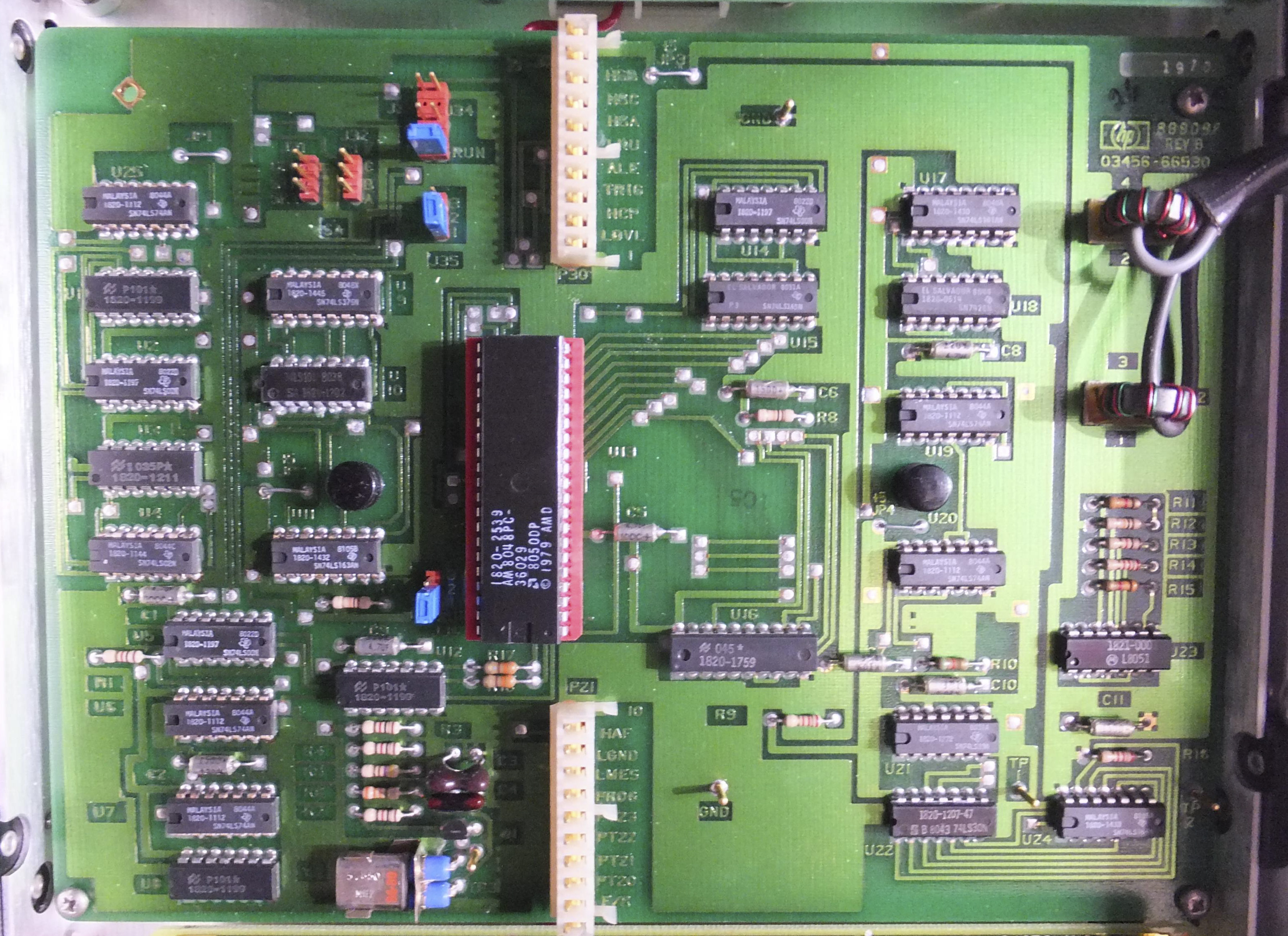
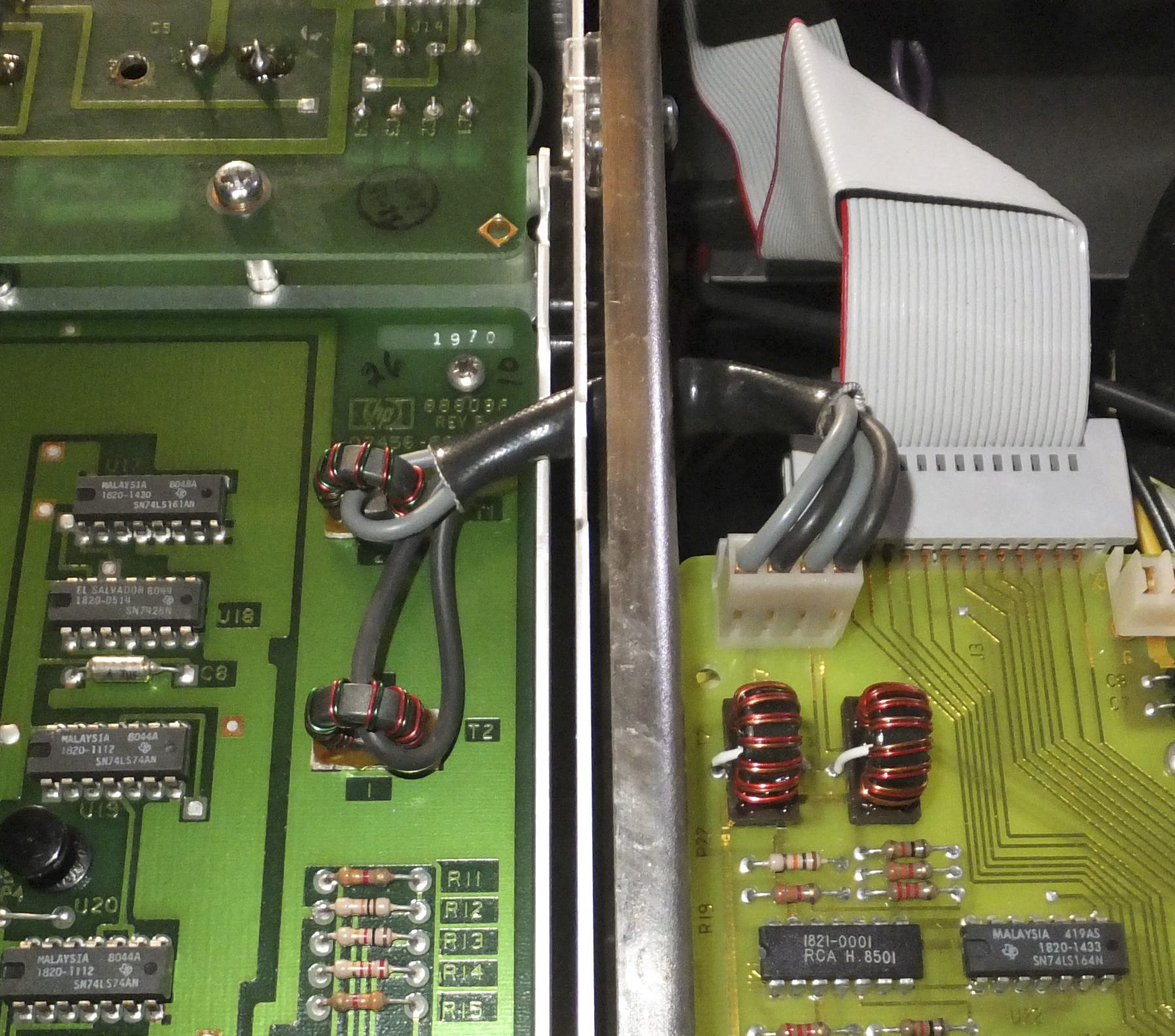
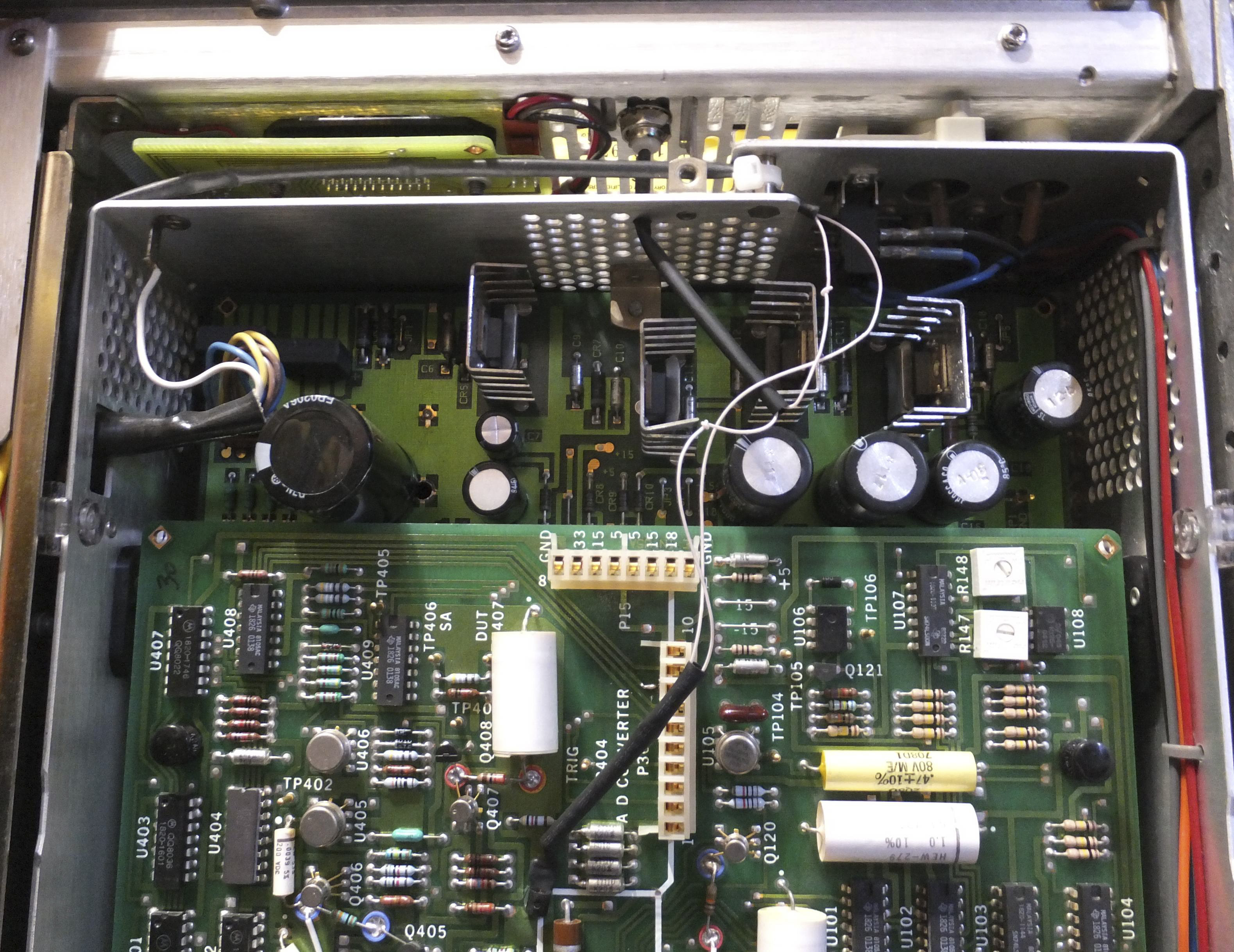
Digital boards repair
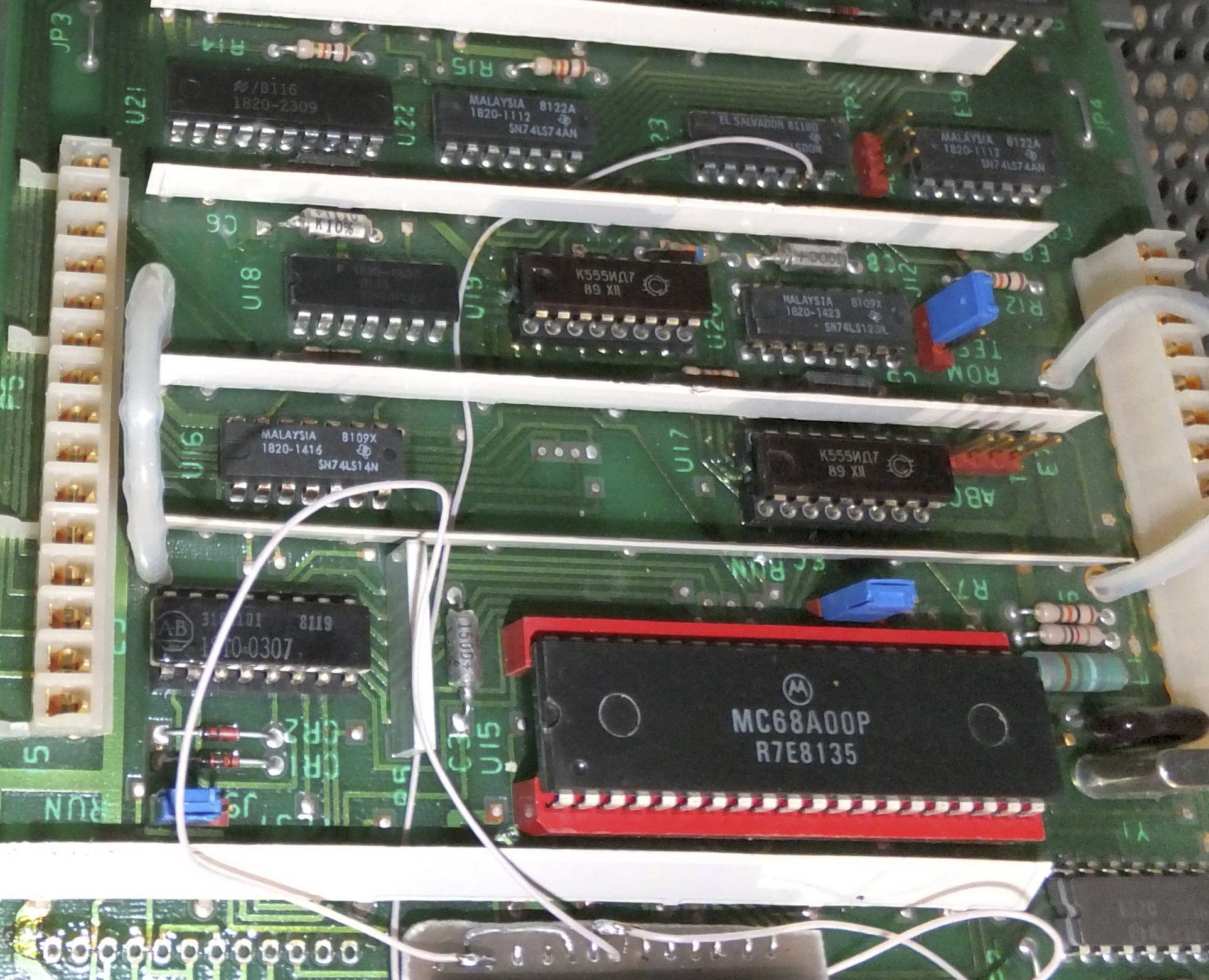
ROM repairs
During power on cycle meter displays welcome message “HP3456”, and then chaos begins. Analysis and disassembly of firmware was done much later, already after repair, so this derailed correct diagnosis to wrong track at first, but let’s not jump and cover all repair flow.
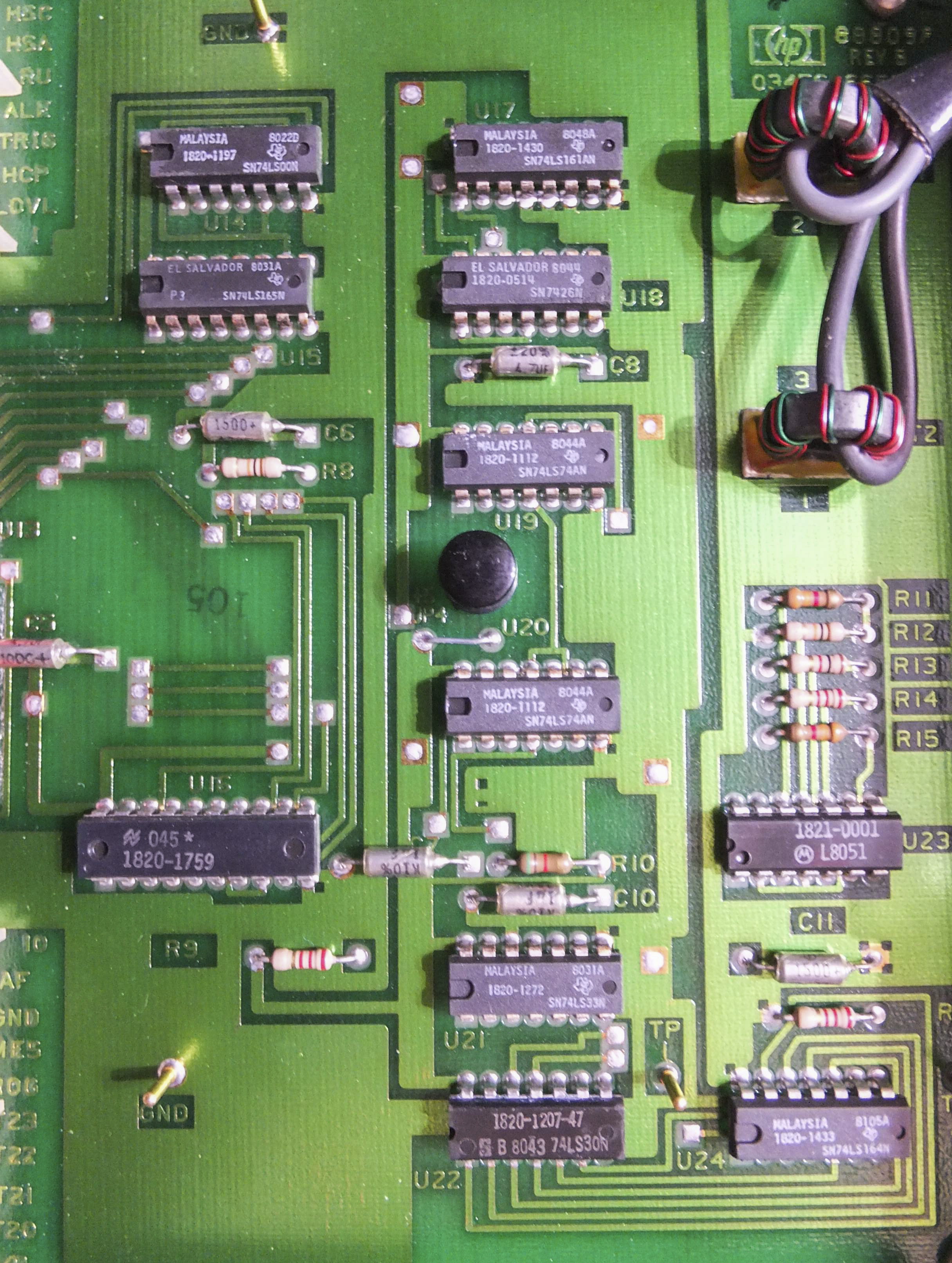
By having this message on power, initial conclusion that processor, address and data bus, as well as RAM and ROM chips are working properly. Also display interface logic was counted as working as well. Suspect in chaotic behavior lied on keyboard interface, as from past experience instruments with stuck keys/faulty keyboards sometimes doing similar things, giving incorrect scan codes and making control UI go crazy. Front panel was disassembled, but no visible damages or faulty parts were found.
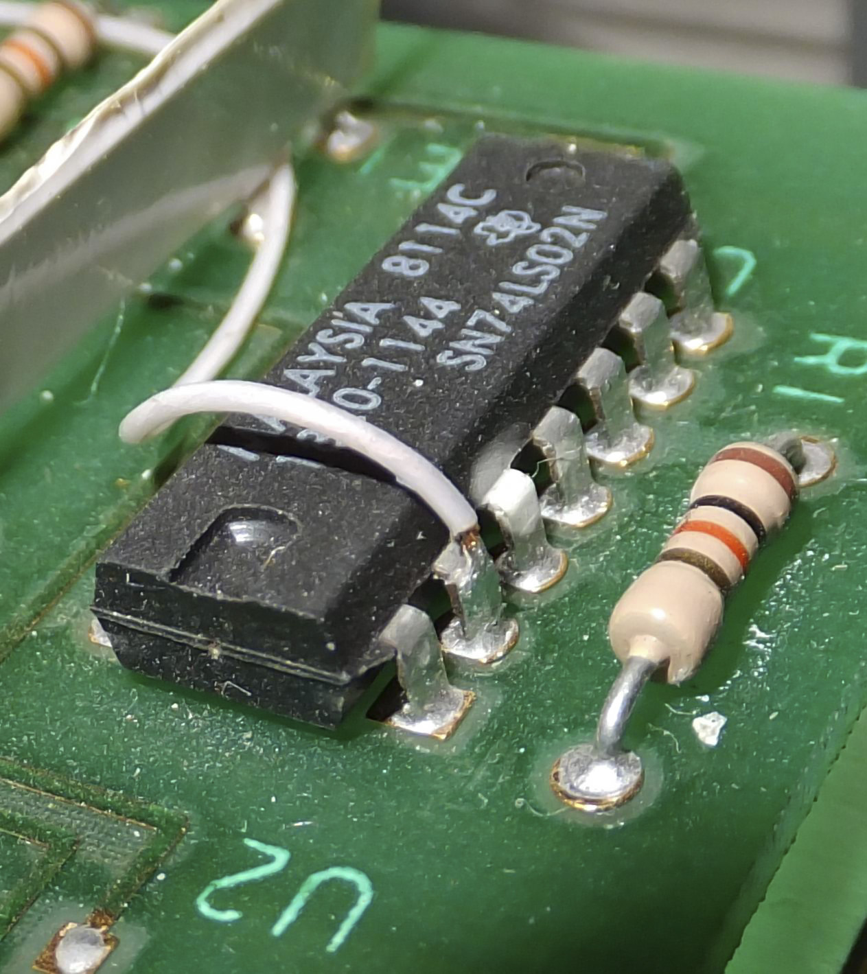
Keyboard driver U21 on A4 PCBA tested OK as well, as there were no digital bus activity on it. This in turn brings decoder logic into question, as keyboard logic should be scanned frequently to check if any keys pressed. U17 and U19 on A4 were replaced, but meter was still doing same thing.
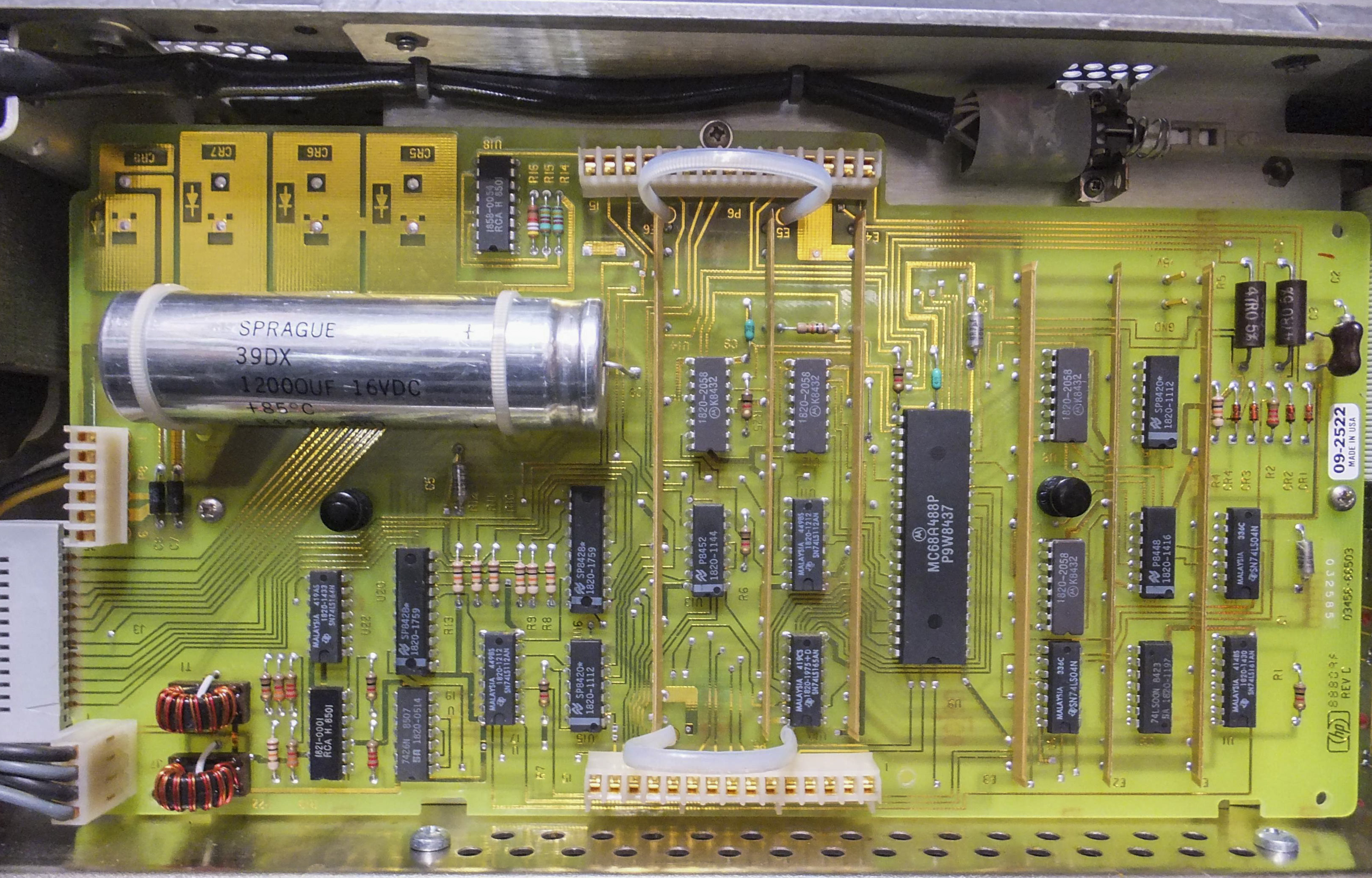
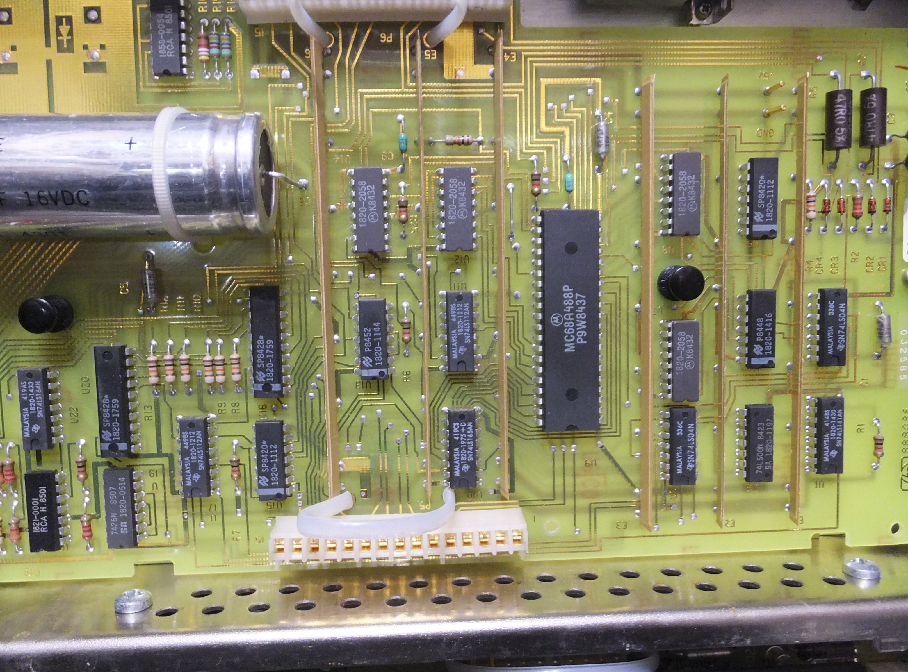
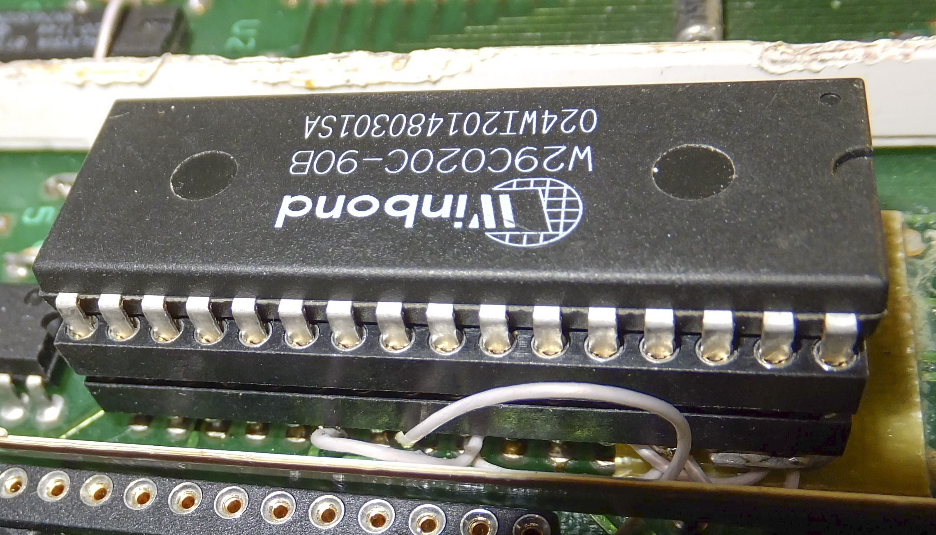
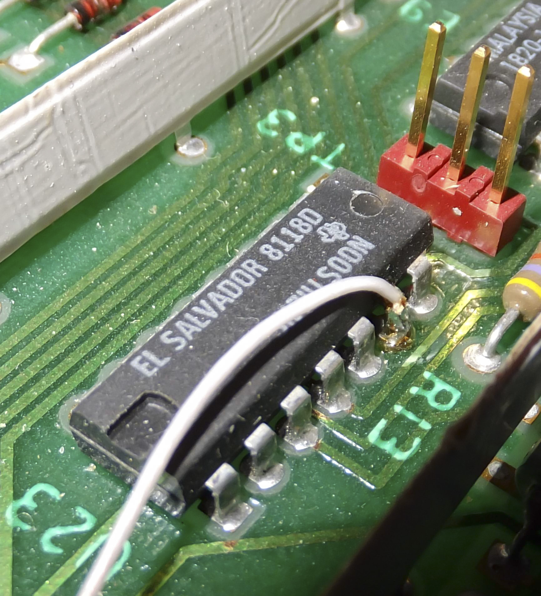
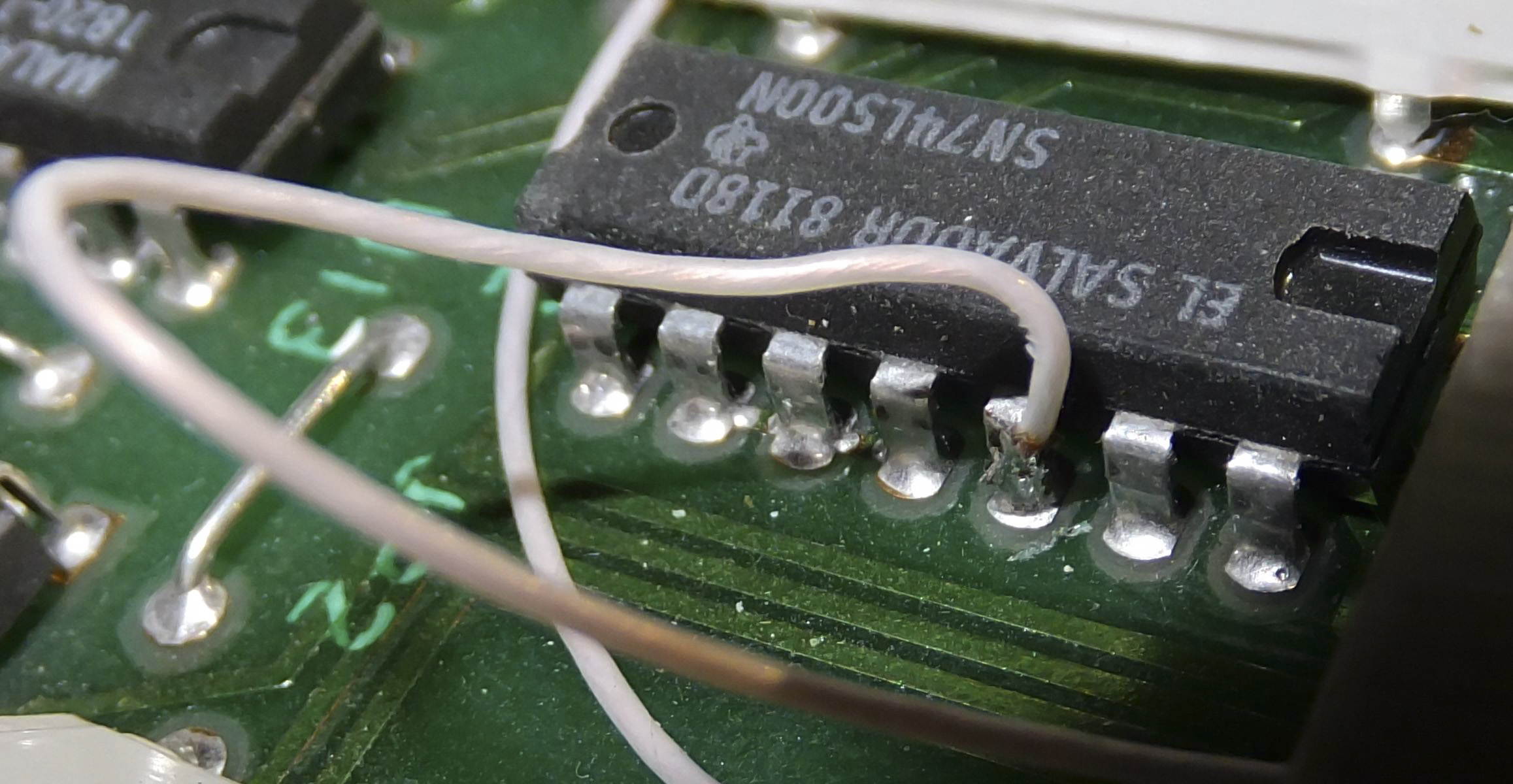
At this point, main diagnosis was reconsidered, as there were online threads, such as [3] and [4], mentioning ROM chips failures. ROM chips were replaced, but since we did not had original IC’s. Not even UV 27xx series, disregarding idea of getting into UV rig and buying extra parts. Since it was a low-cost restoration project, some salvaged parts suitable up to task were found. This was 2MBit BIOS ROM MX29F002 from old ABIT PC motherboard. It’s not pin compatible, so some modifications were performed to fit it in:
- Carefully, to avoid PCB damage, removed original ROM chips.
Since new ROM have 32 pins, instead 24 on original circuitry, direct replacement would not work. So IC socket was installed, but due to larger size and to avoid possible short-circuits I made insulator from thin PCB layer, glued to nearest ROM footprint.
Also due different pinout definition, some pins from socket were isolated from board, so we can solder wire and reroute signals to proper locations. Isolated pins are: 1, 2, 3, 4, 22, 24, 25, 28, 29, 30, 31, 32.
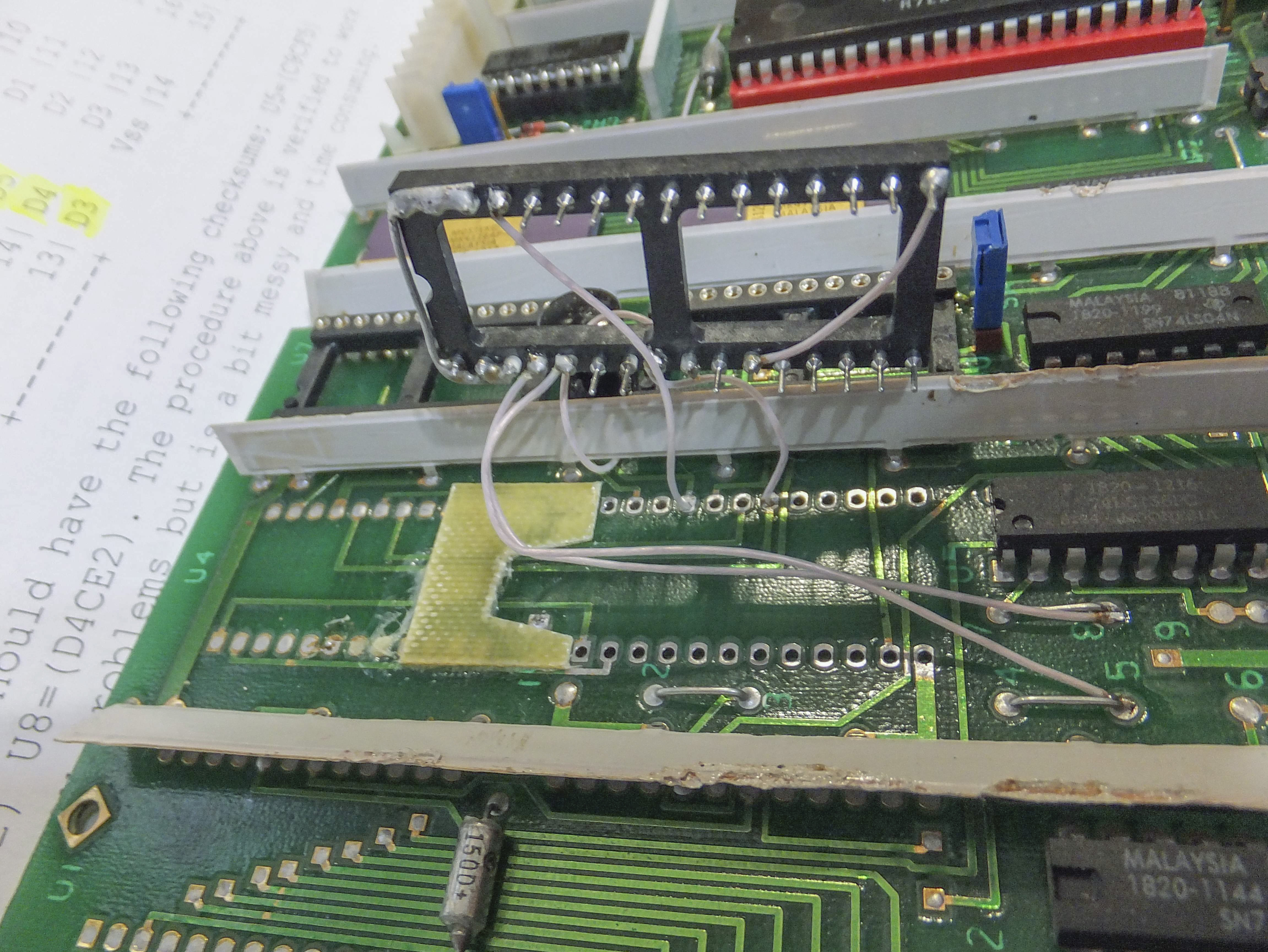
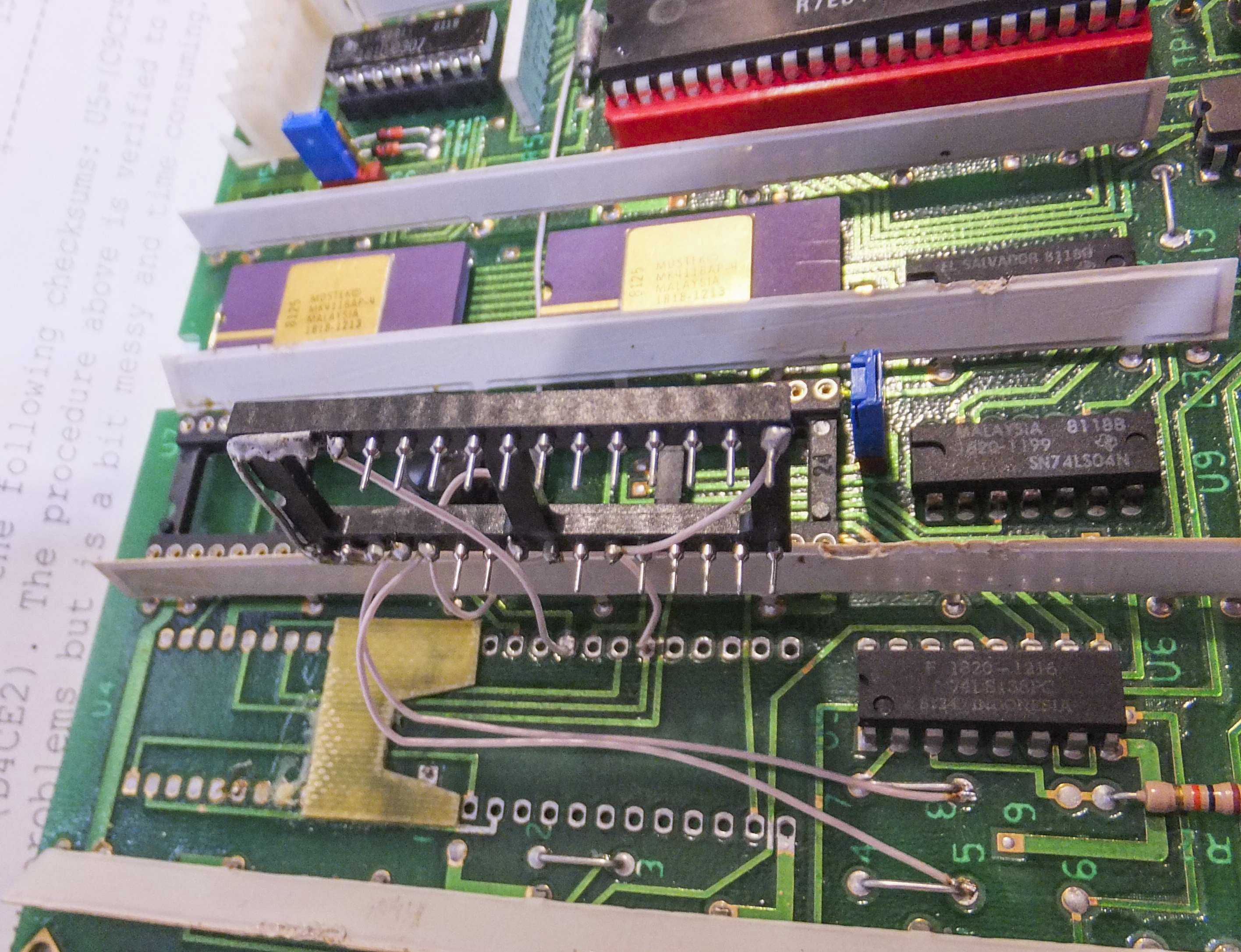
IC socket was soldered on PCB in a way, so pin 16 fits pin 12 of original ROM, so we get data bus and some address signals match original layout.
Rest of isolated pins were connected in next fashion (marked blue in A4 schematics):
- Pins 1, 2, 3, 30, 31, 32 were powered from digital +5 VDC;
- Pin 22 grounded (just a short to pin 16 on socket);
- Pin 25 routed to pin 18 of original ROM location;
- Pin 4 routed to signal А12 from original ROM’s pin 21;
- Pin 28 routed А13 from jumper pin 4-5(JMPRB);
- Pin 29 routed А14 from jumper pin 7-8(JMPRC);
- Pin 24 routed to chip select CS from U23 pin 6 (А4).
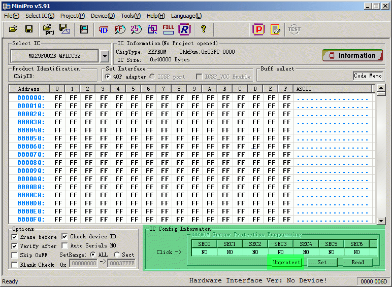
MX29F002 was fully erased in programmer, as well as disabled boot-block protection. ChipProg procedure was simple, as entering “CHIP PARAMETERS”, selection “Disable protection of all blocks”, so BIOS chip becomes simple ROM memory. Sure, most of our readers can adopt this for their specific ROM programming hardware.
Here’s example screenshot for MiniPro with highlighted protection settings:
Latest 256Kb was used, downloaded from rfscientific.eu. They also have some other firmware dumps. Thanks for sharing firmware, as it’s often a problem finding binary dumps for obsolete instruments.
This firmware dump can be flashed once to ROM area 0×38000h – 0×3FFFFh, or can be simply written 8 times, so with any upper address combination, which are actually not used in meter’s normal operation, we still can get firmware. Somewhat a backup feature for future-proof operation.
| Start offset | End offset | |
| Section 1 | 0×00000h | 0×07FFFh |
| Section 2 | 0×08000h | 0×0FFFFh |
| Section 3 | 0×10000h | 0×17FFFh |
| Section 4 | 0×18000h | 0×1FFFFh |
| Section 5 | 0×20000h | 0×27FFFh |
| Section 6 | 0×28000h | 0×2FFFFh |
| Section 7 | 0×30000h | 0×37FFFh |
| Section 8 | 0×38000h | 0×3FFFFh |
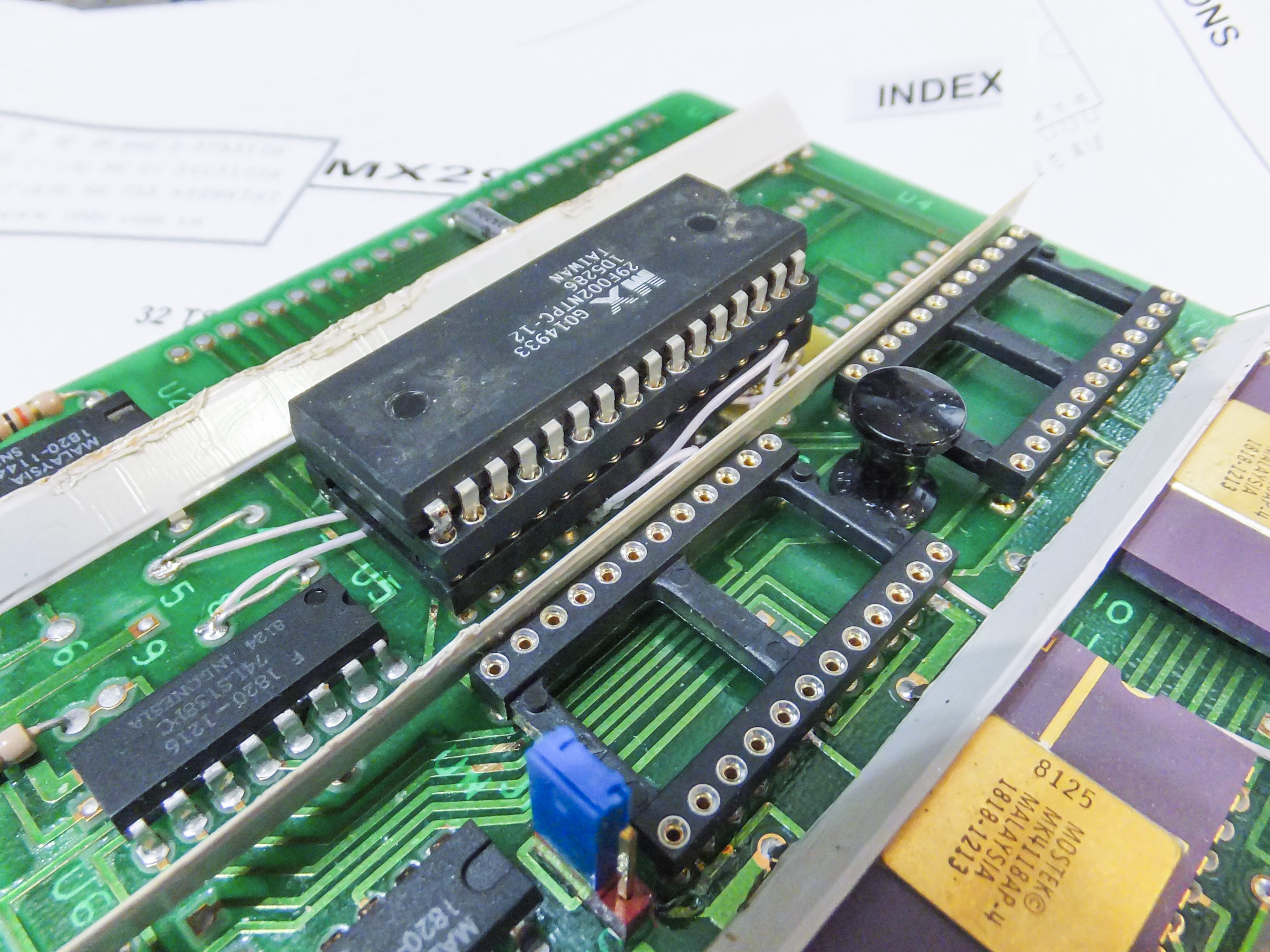
You can also spot second IC socket on photo. This is due simple reason, as my MX29F002 had missing data pin, so had to fix with extra bit. To avoid damage of socket mounted on PCB, this intermediate socket was used to hold fixed ROM chip.
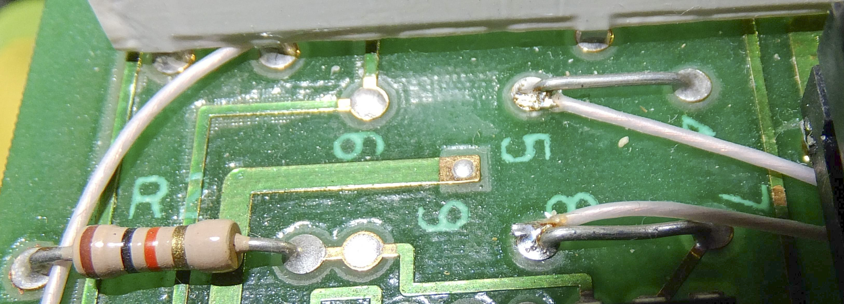
RAM repairs
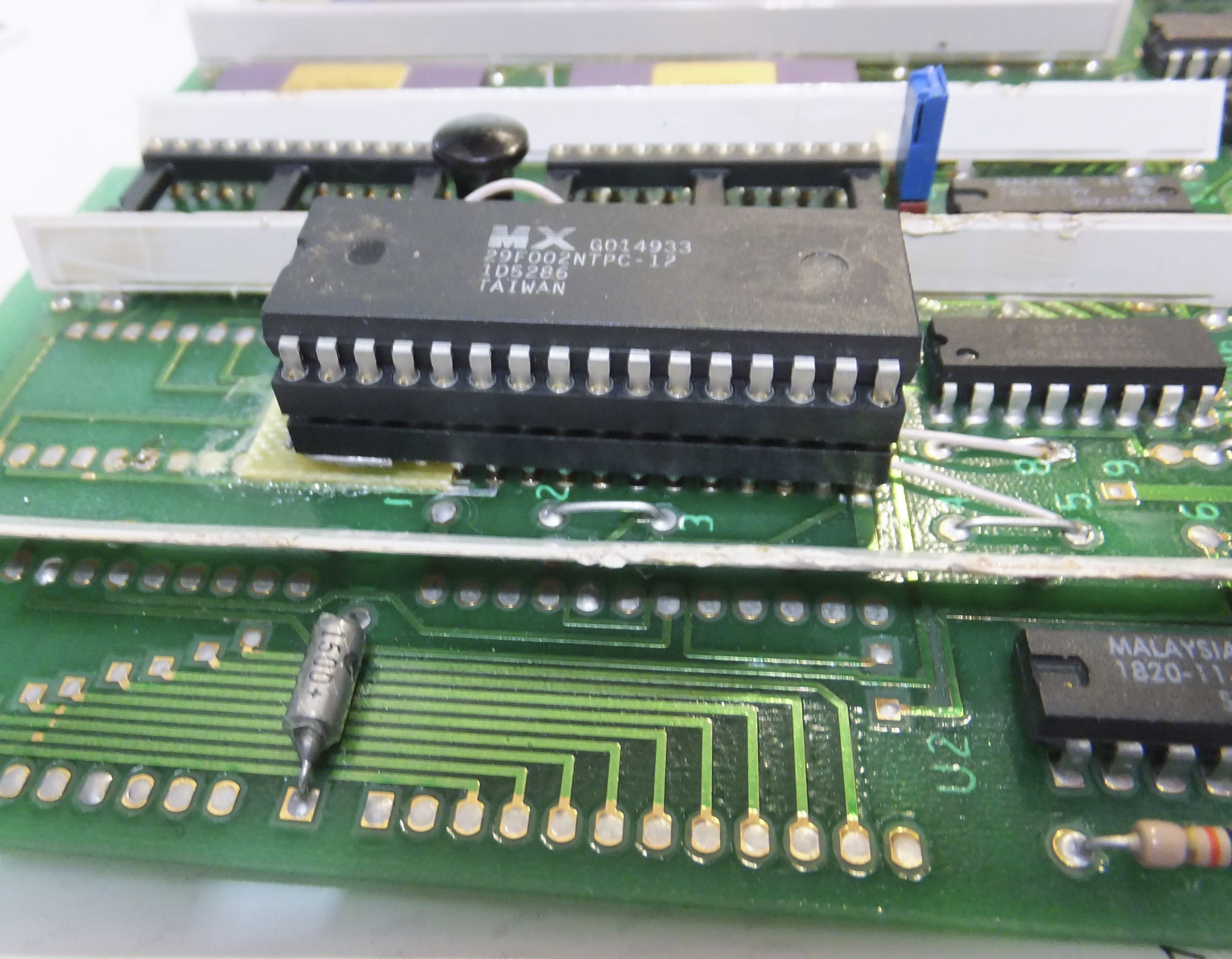
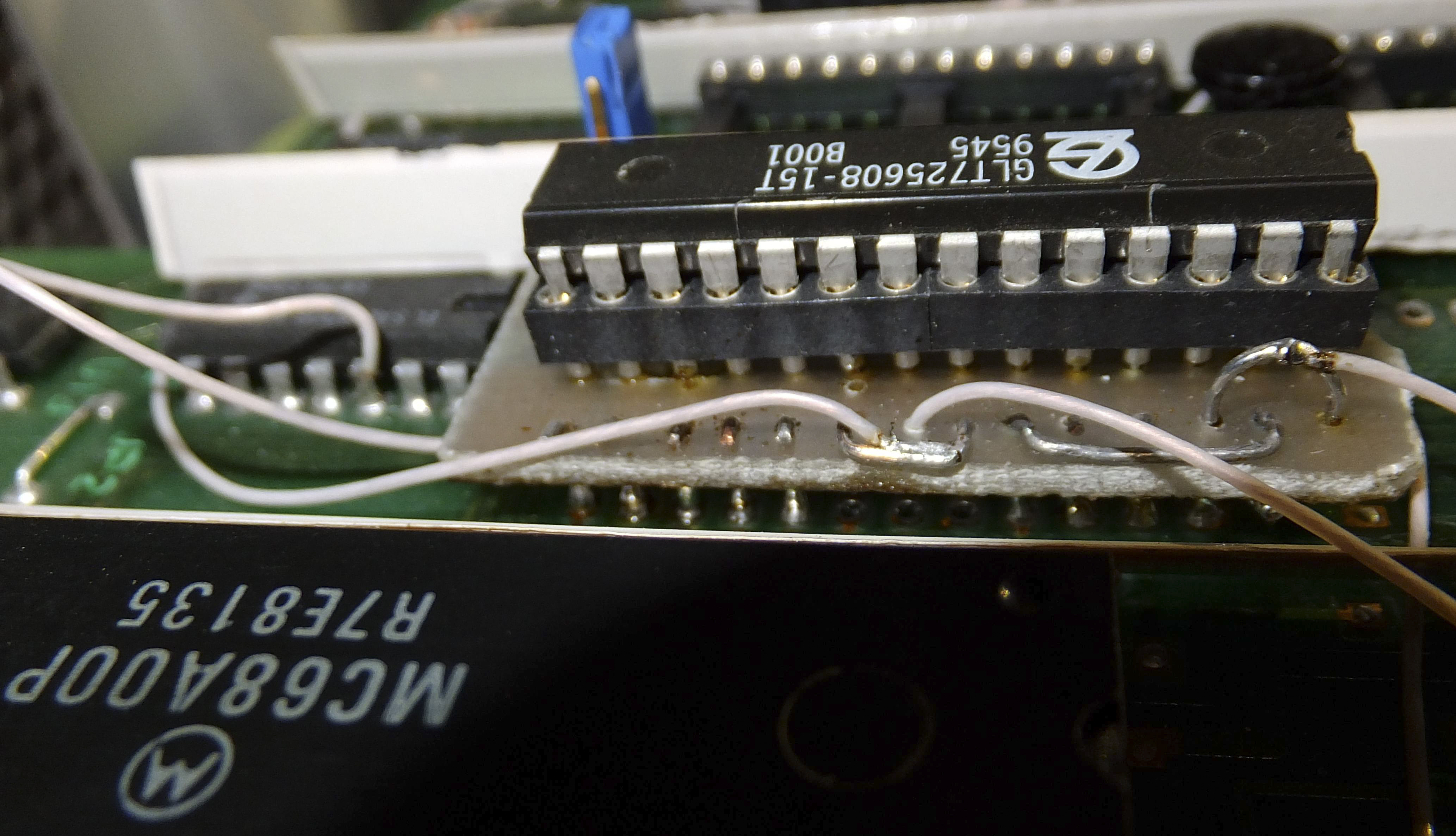
Moment of truth… Powering on meter, same problem and chaotic operation. So problem is not in ROM, or not only in ROM. There is last thing left before actual processor – RAM chips. Again search for obsolete DIP-package chips, without any progress.
I did not have anything similar to 6116 series RAM, and only suitable RAM was GLT725608, which was used as cache-SRAM used on ancient i486 motherboard. It had narrow package, so 28-pin socket (fixed up from two 14-pin IC sockets) was installed into intermediate adapter.
Everything else is similar to ROM repair workflow – careful removing old RAM chips from A4 PCB, soldering some socket pins with copper studs into PCB, so pin 14 of socket match PCB’s pin 12. Ground to ground, data bus signals to data bus.

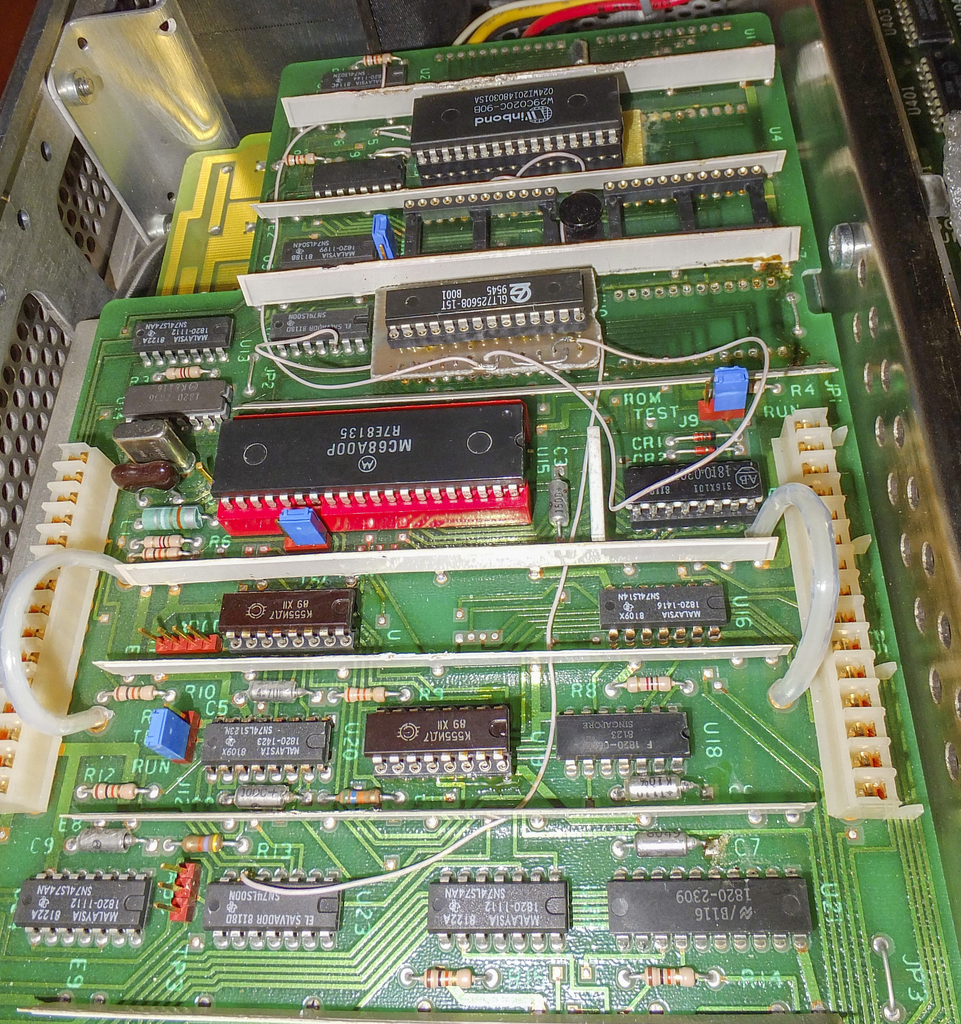

Isolated pins on adapter socket: 1, 2, 21, 23, 26, 27, 28.
Signal wired like shown on digital board A4 schematics (marked green):
Pins 1, 2, 23, 26, 28 connect to digital power +5 VDC;
Pin 21 – wired to address signal A10 taken from U12 pin 12. In original schematics, signal A10 is used to switch which RAM chip is being accessed, and for reliable operation delay line, consisting of logic in elements U12d, U12c, U9f, U9e was used. Our RAM chip have more density, so we don’t have to use this workaround, and just enough to use direct connection to address line A10;
Pin 27 wired to old pad for pin 21 (write enable signal WE).
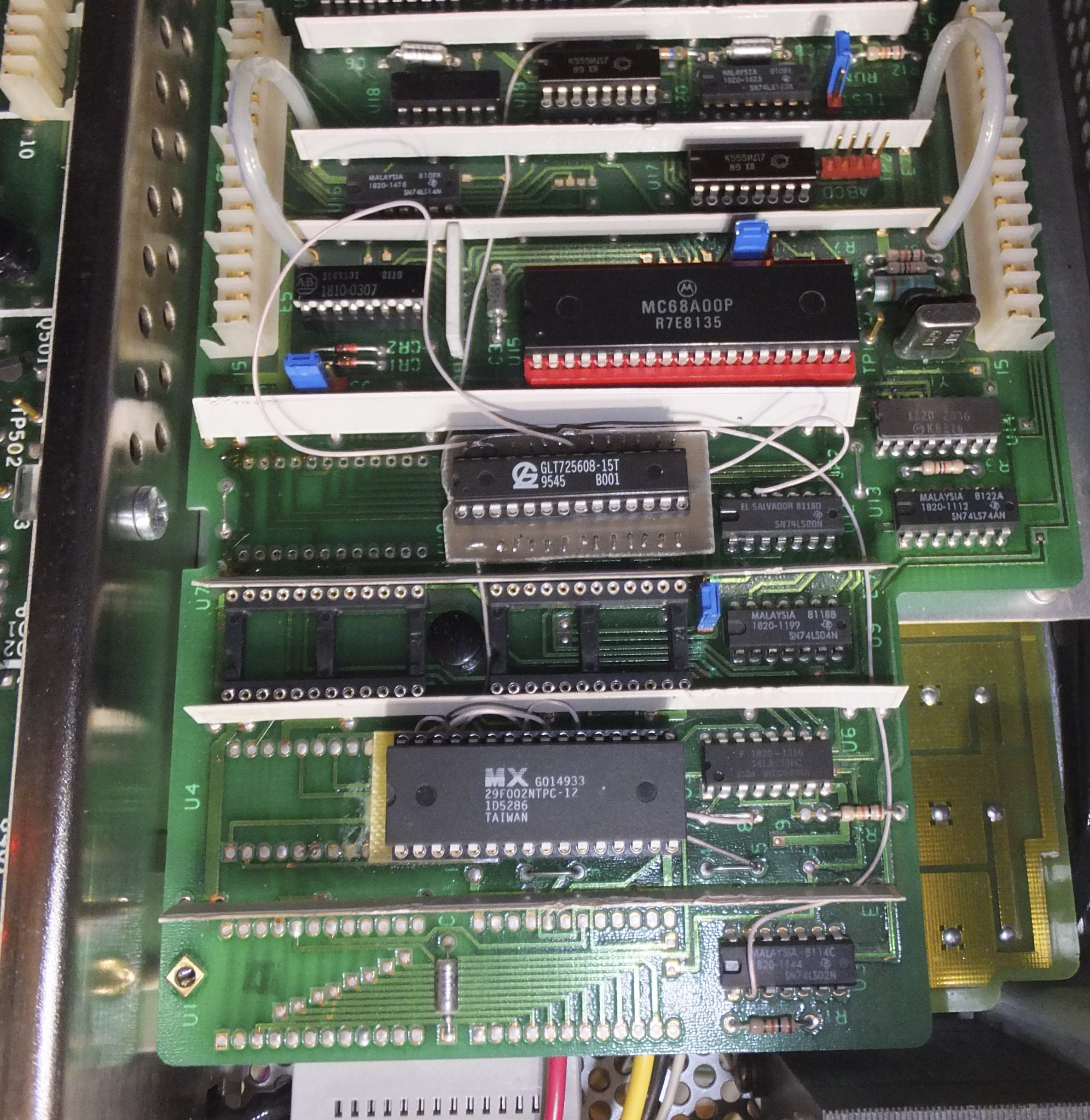
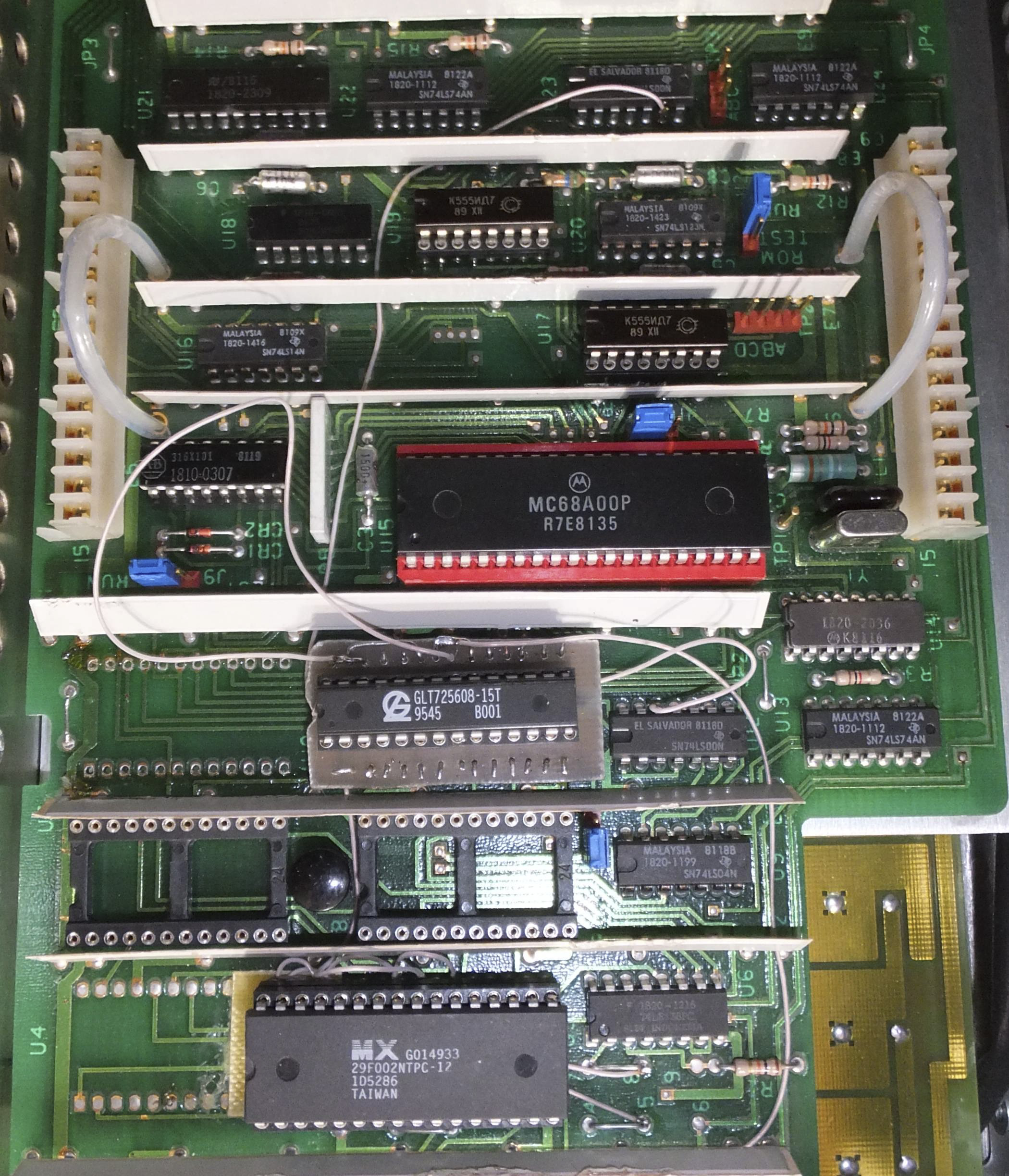
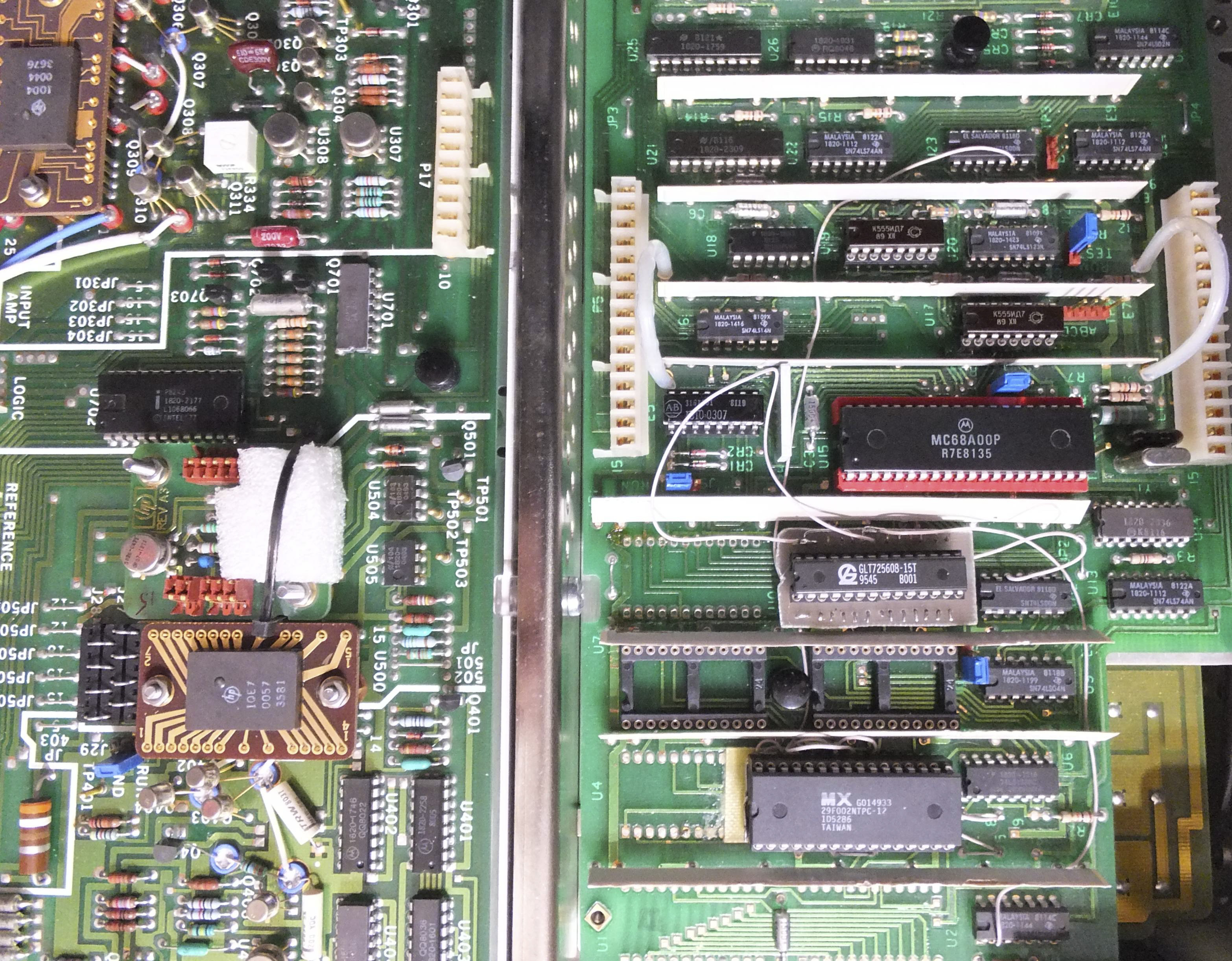
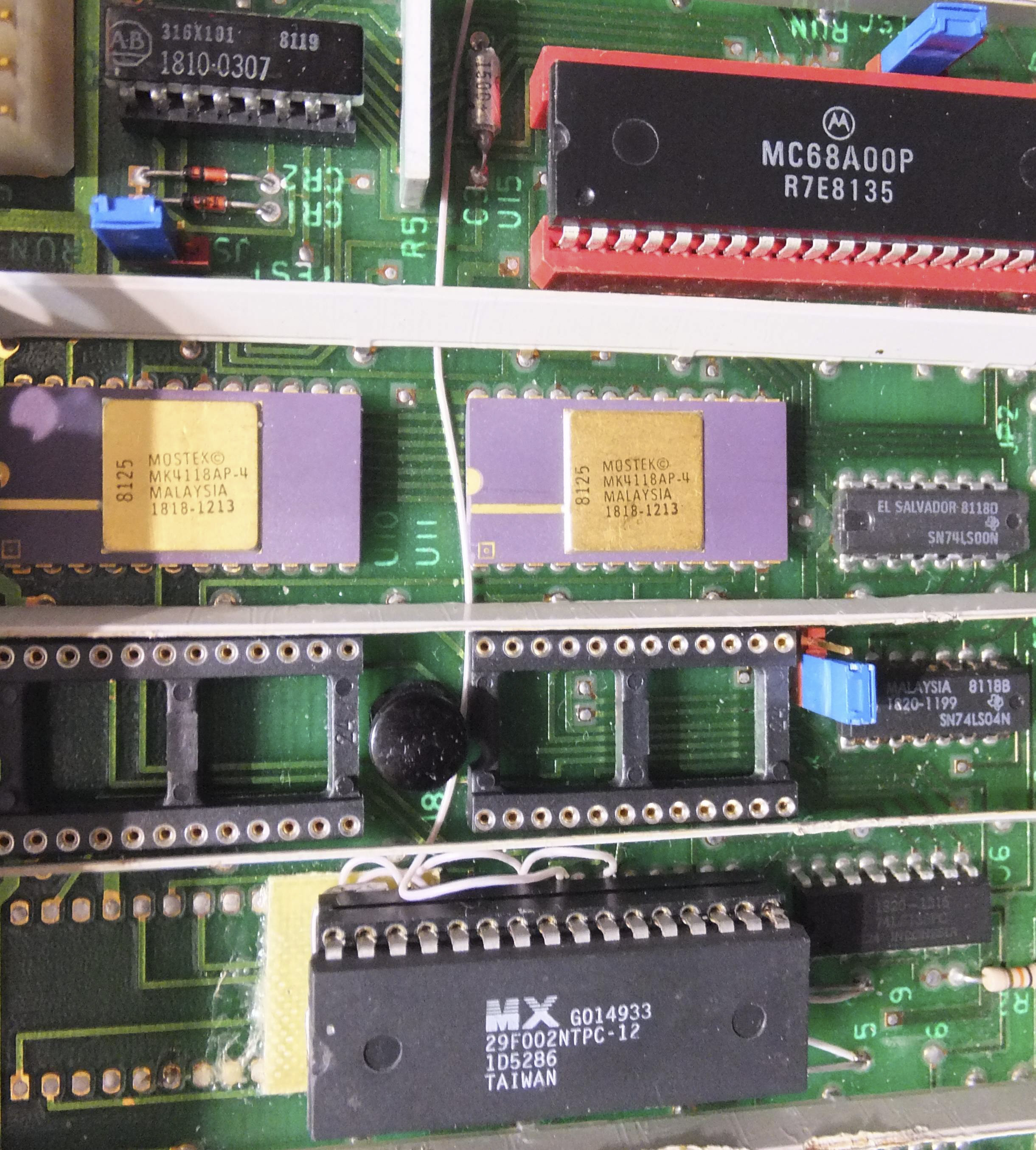
Now, after RAM replacement, instrument finally came back to life. Self-test discovered inguard-controller failure. In my case processor i8048 was installed in socket. Chip temperature was OK, so I just removed chip and installed back in. Immediately instrument went to normal operation and show few counts on display. So I went ahead and replaced old socket with modern high-quality collet-type socket. HP in 3456A-13A Service note recommends to solder chip down to PCB.
![]()
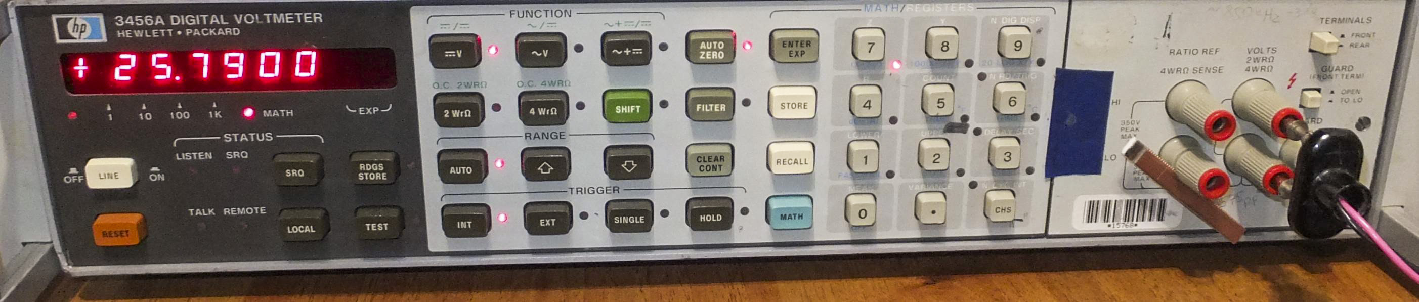
Multimeter booted fine and now able to operate normally.
Let’s take a summary on repairs performed:
- Decoders and ROM chip were replaced without actual need.
- Repair was performed for power supply, replaced capacitors.
- Replaced RAM and inguard-controller socket to collet-type one.
Modifications
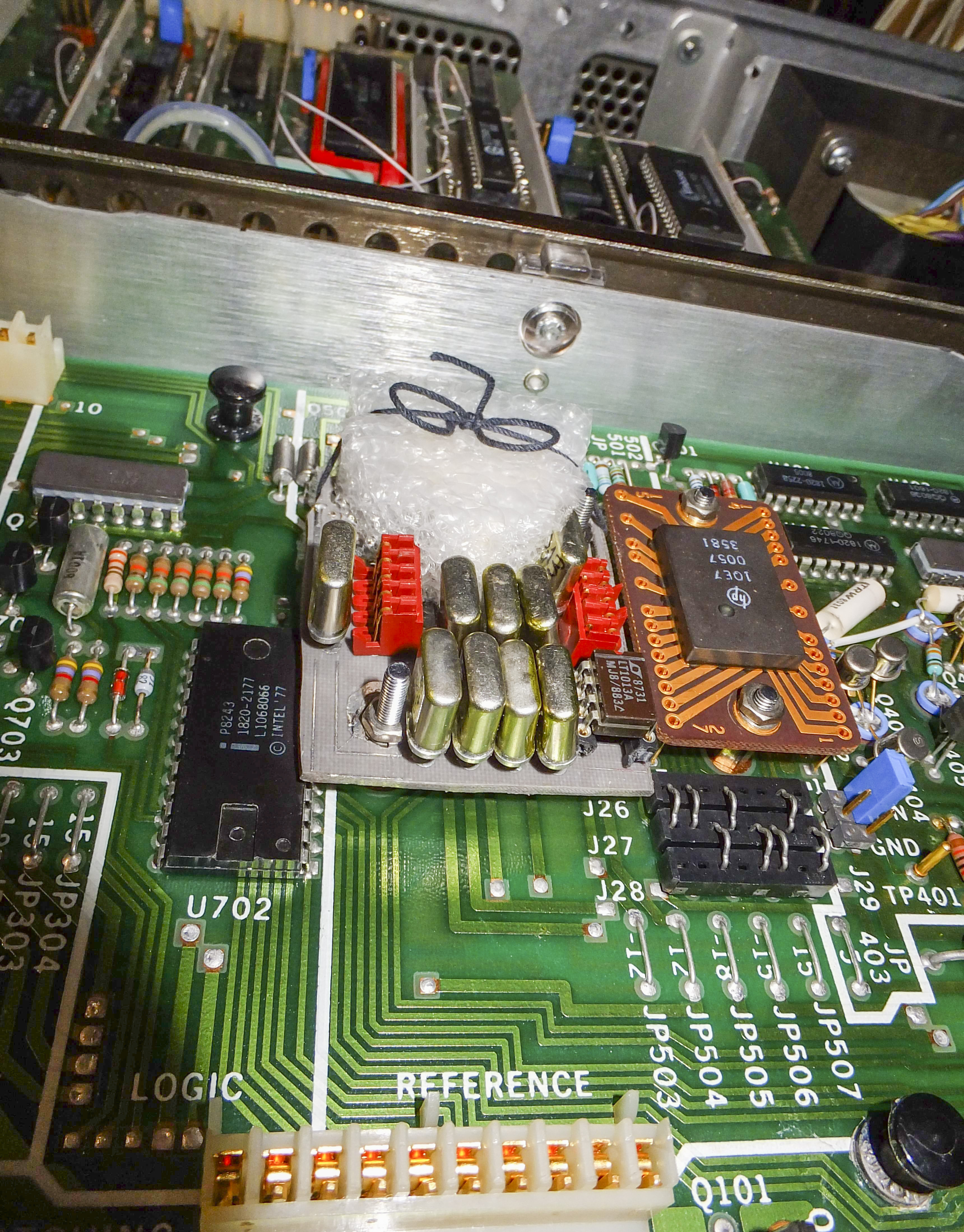
Right after repair and initial checks, instrument was modified – installed temperature sensor, improved thermal and air insulation around voltage reference zener, and later whole reference module was replaced with DIY triple “LM199-based”:“LM199”:/doc/HP_Agilent_Keysight/3456A/pdf/lm199.pdf module. Results in the end of this article were achieved after all these improvements completed and installed.
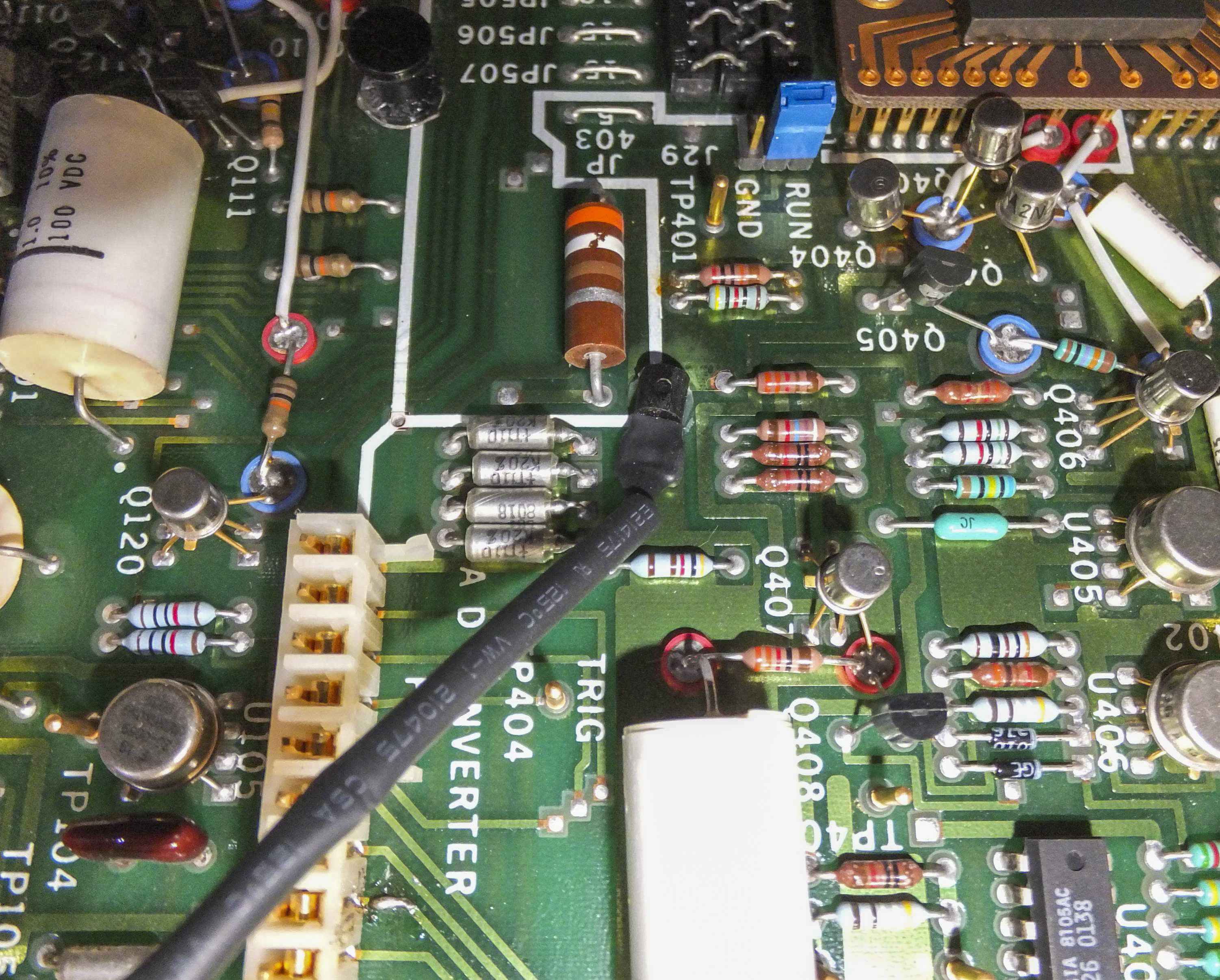
Temperature sensor
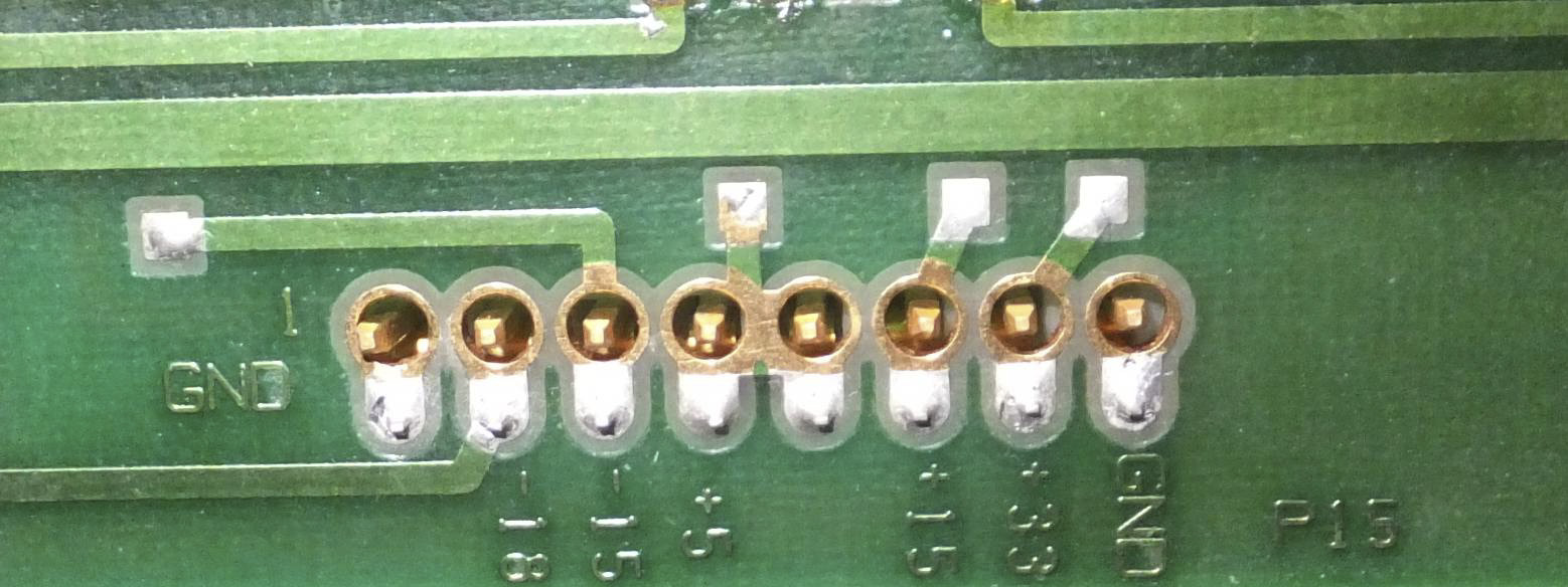
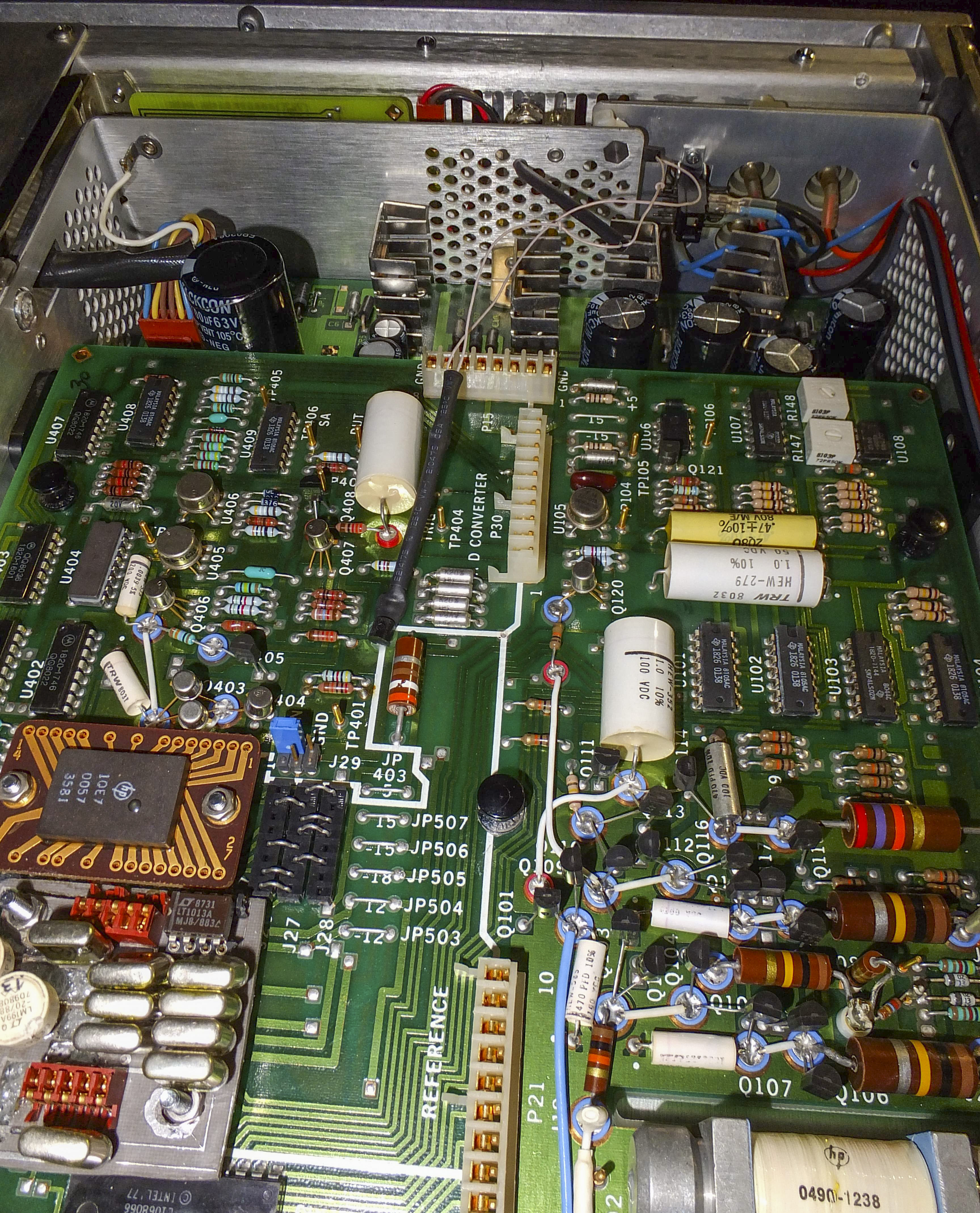
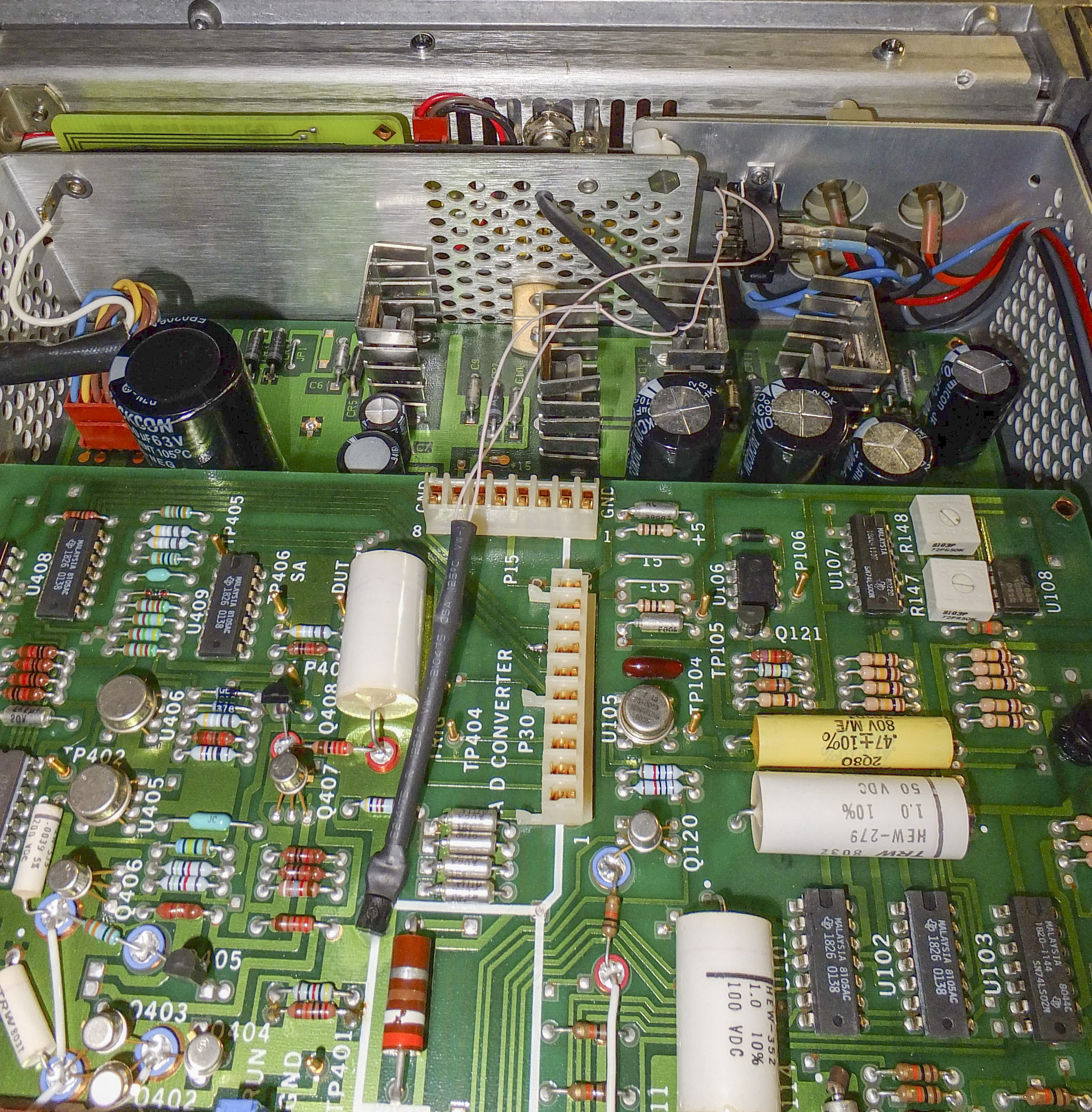
Additional temperature sensor (LM135) was installed to allow monitoring internal instruments temperature. This was performed by wired connection, protected with heatshrink tube. Sensor IC itself was glued down on A/D board over massive ground copper pour for better temperature accuracy. Sensor is powered from huge digital board’s 12000µF. Ground return was connected to chassis ground, so this does not introduce noise to analog circuitry.

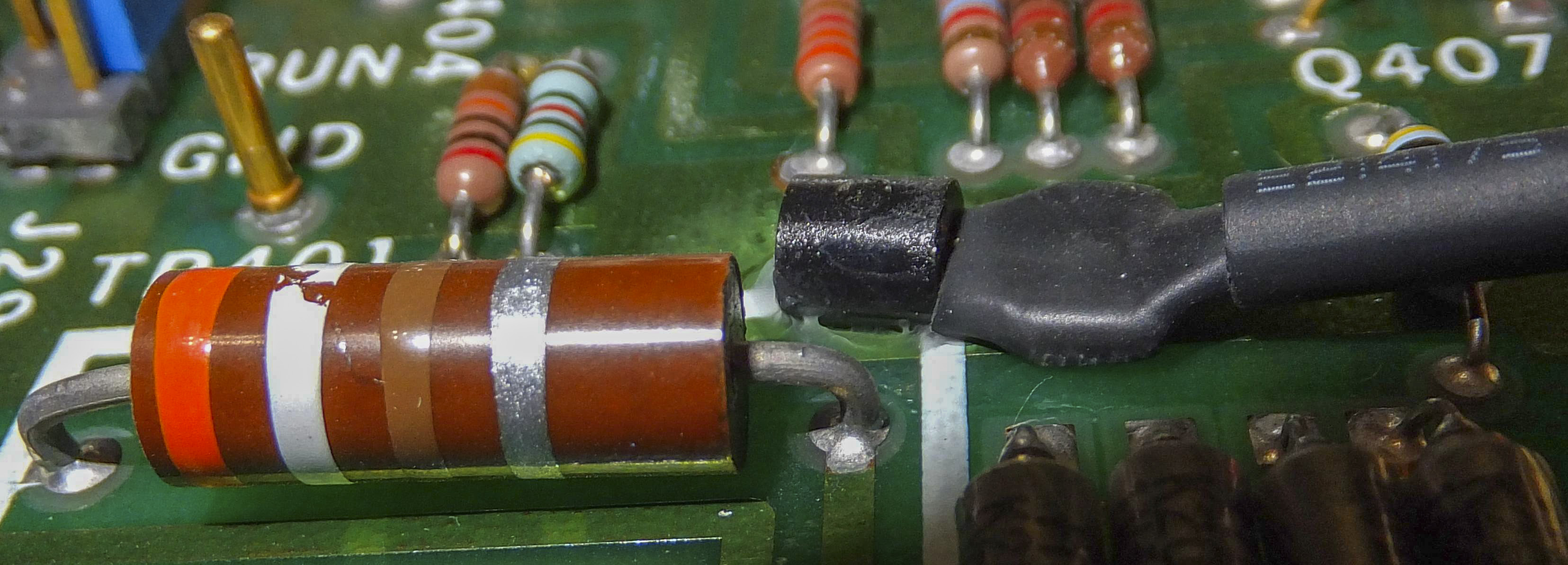
Current limit resistor was connected in series and heatshrinked as well. BNC-port with temperature output was installed on rear instruments panel, using airflow grill. One of grill sections was cut out with pliers. Avoid any drilling or milling, this easily can cause little metal bits and pieces stuck somewhere on PCBs and cause problems later.
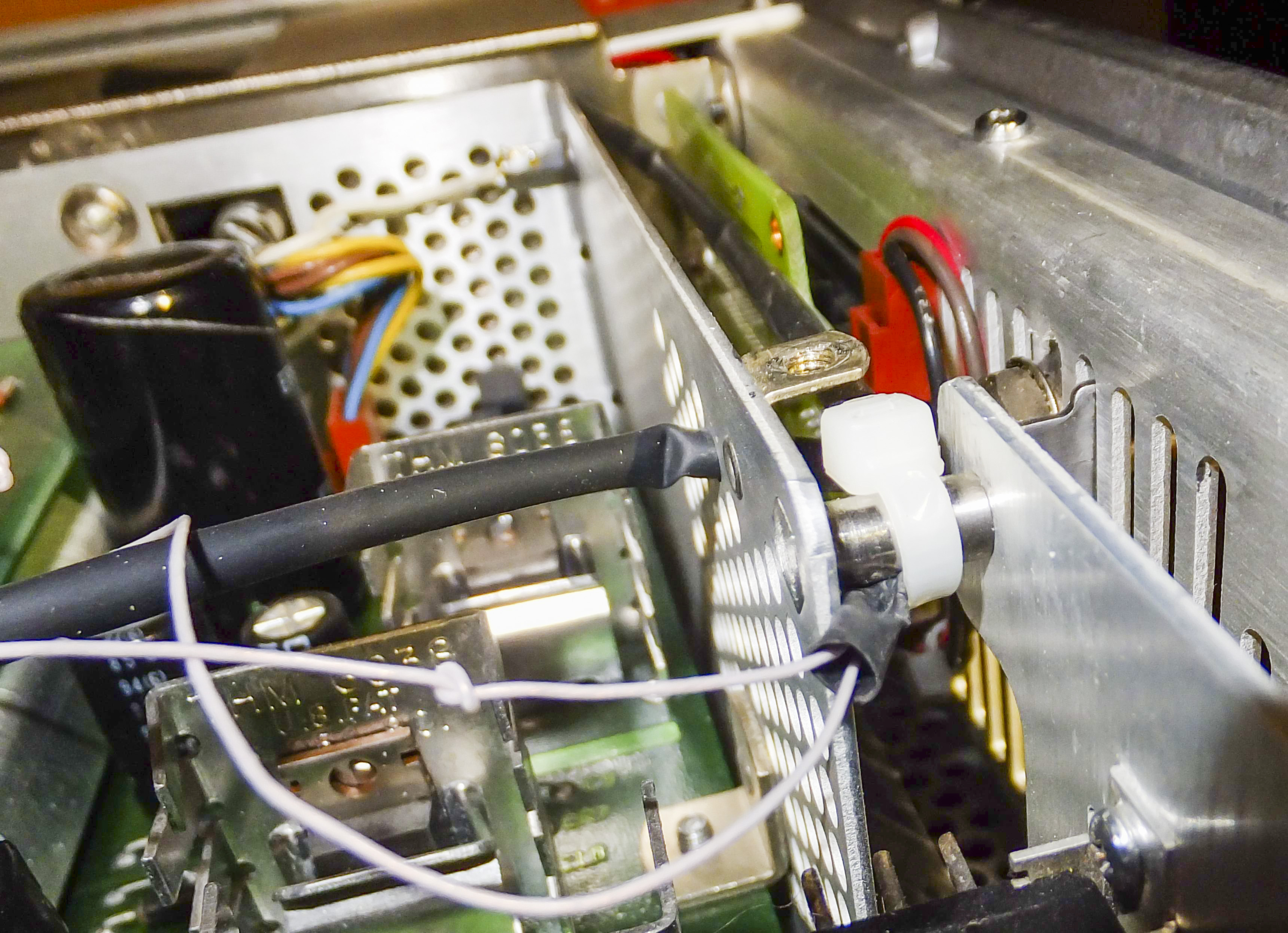

Thermal sensor wiring was routed using existing holes and areas, as you can see from provided photos.

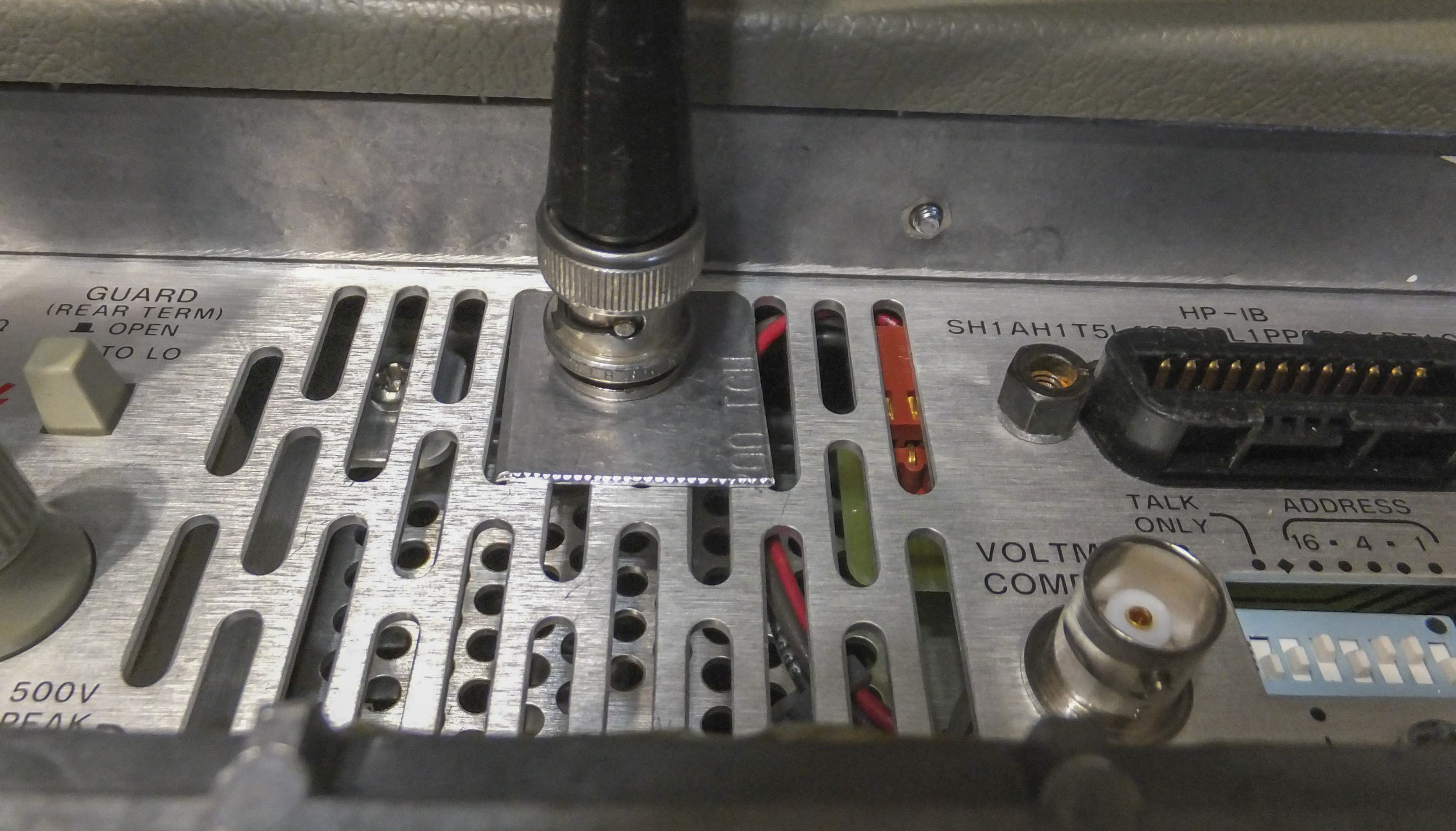

Thermal sensor output can be connected externally to rear multimeter terminals.
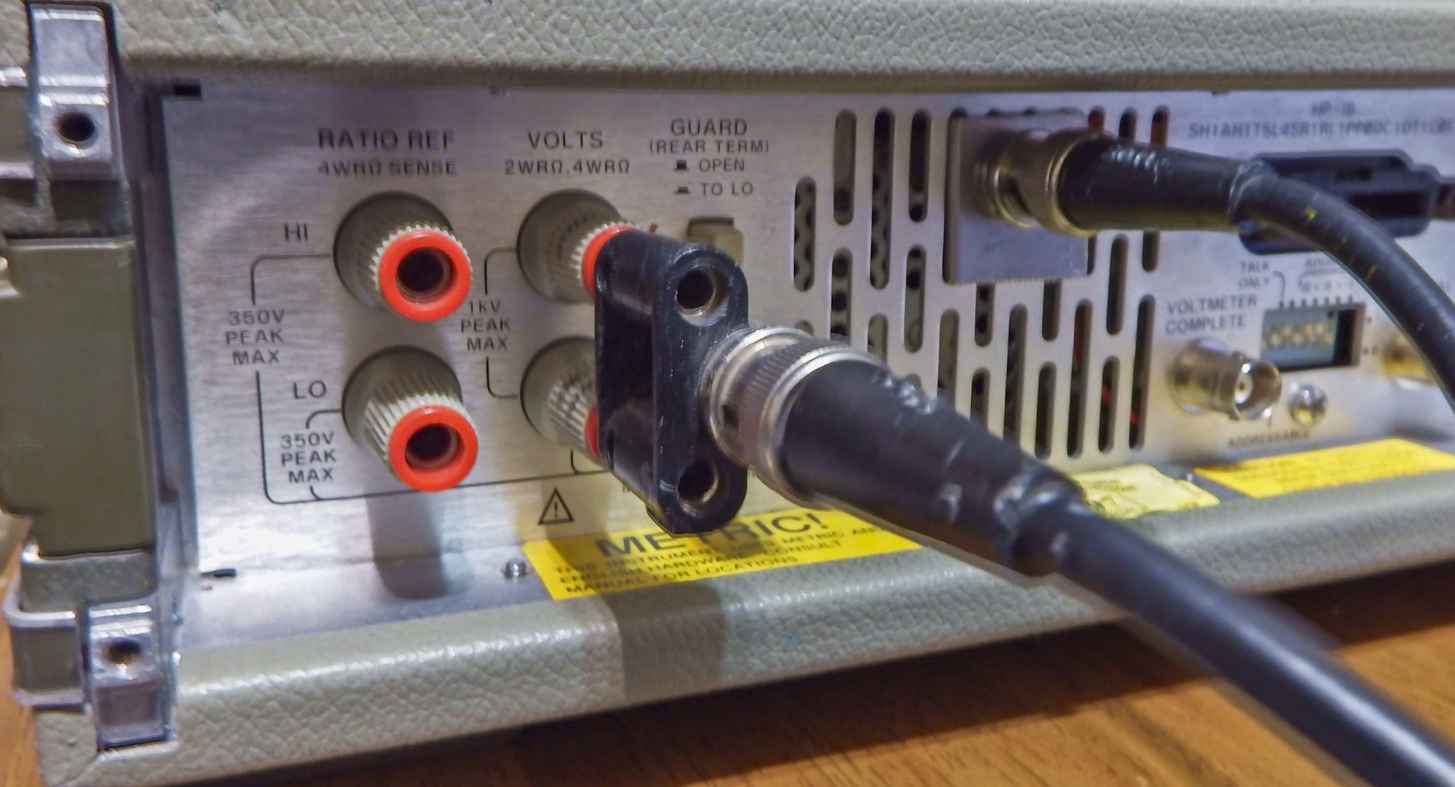
Temperature measurement can be performed on both inside meter (left photo) and outside ambient (right photo):

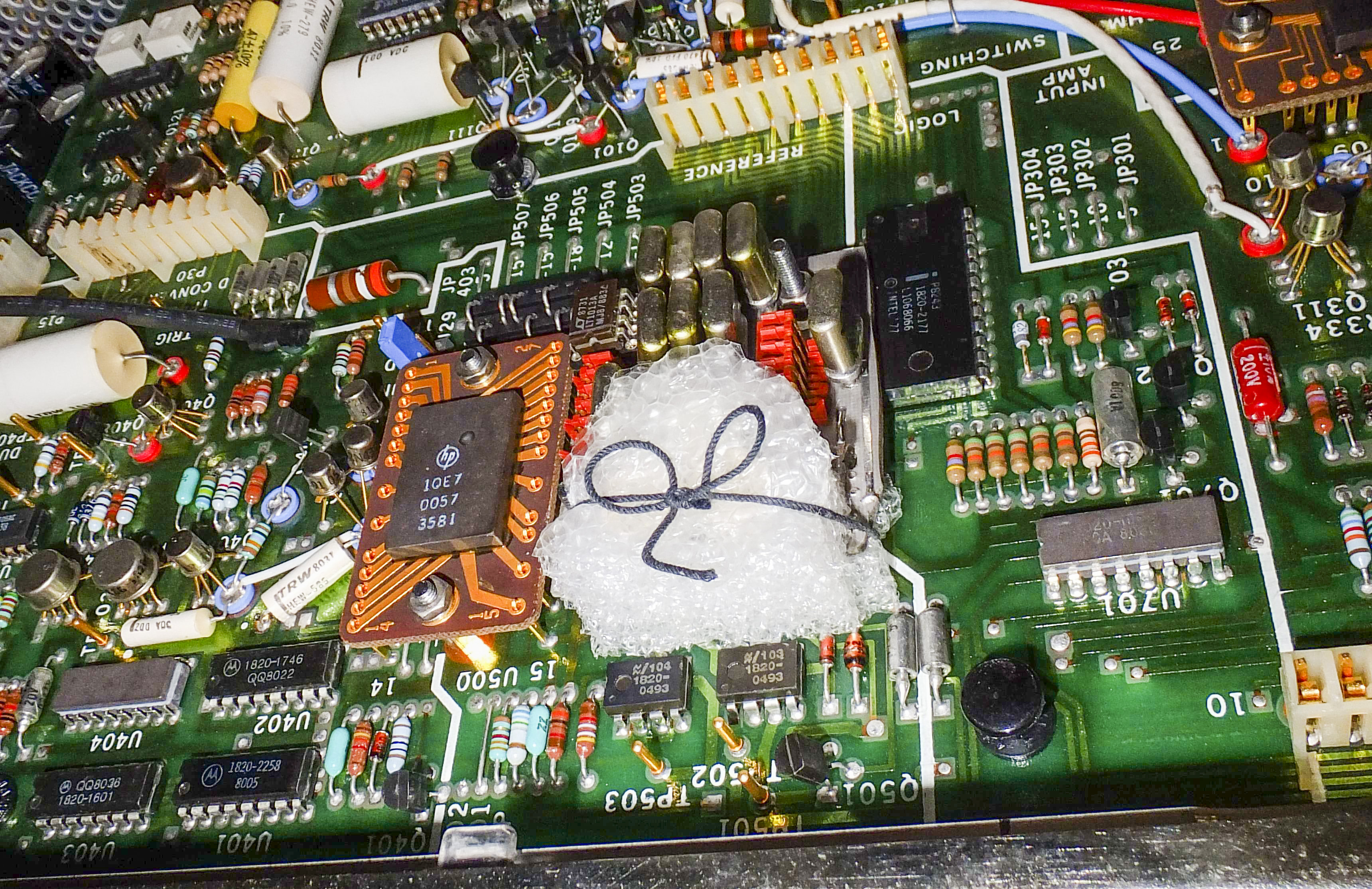
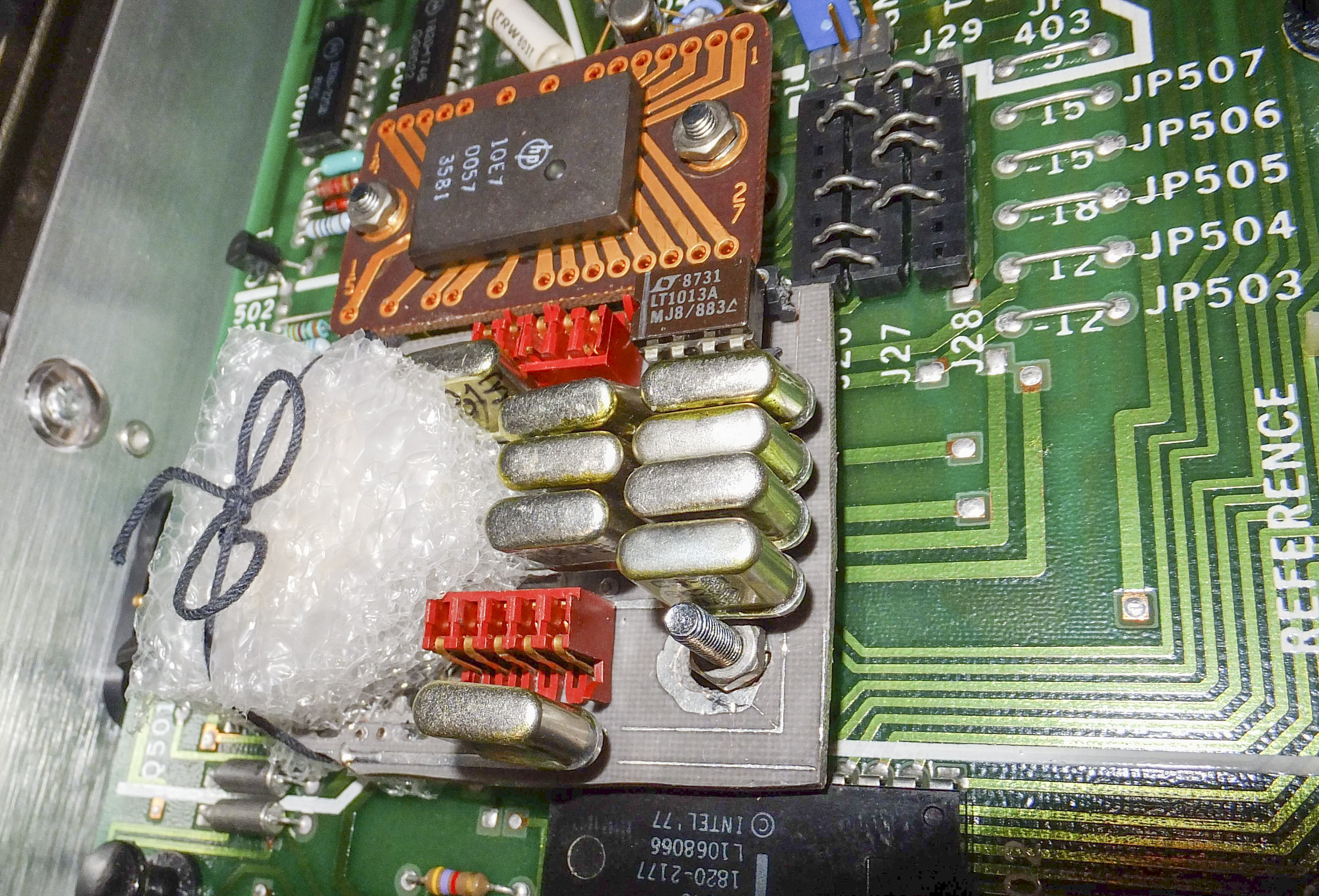
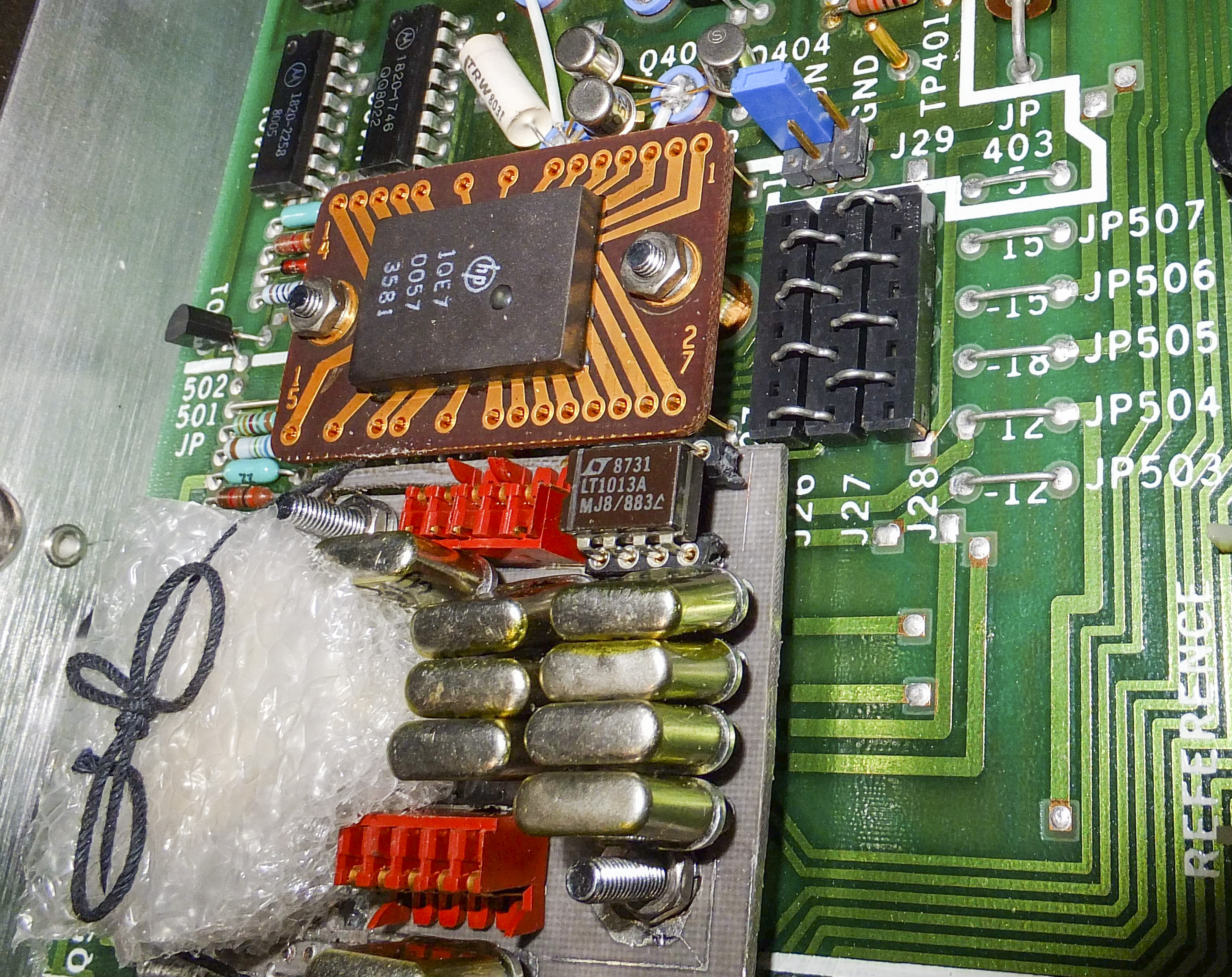
Voltage reference improvement
Members of EEVBlog forum got answers from Bob Dobkin, designer of famous LM399 and LTZ1000 about some precision enthusiasts questions. Decided to try some of these notes to implement on this particular instrument restoration project.
Most interesting notes are quoted here below:
Note that for LM399-based designs, the slots in the PC board [plus a lot of insulation top and bottom] make sense-- Bob said that the less power the heater requires, then the more stable the output voltage will be.  So, in this case, the slots [plus insulation] are helping with this.  Oh-- and he also said that the LM399 should be run at about 1mA of Zener current for best stability.  The more stable you can make the Zener current, the more stable will be the output voltage.  He said that there is about 1uV of voltage change for 1uA of current change.

If properly insulated, an LM399 can have a ppm/K figure of between 0.1ppm/K to 0.2ppm/K-- the data sheet is *very* conservative.  [Note that the DMM manufacturers are not insulating these other than the plastic insulator that they come in-- they would benefit by better insulating the top and bottom of the LM399 to keep the heat in, and the heater power down.]
So given this information, it’s clear that voltage reference long-term stability can be improved by reducing current for LM399’s internal heater. Since all thermal control and regulation is done internally on-chip, there is only one way to do such – reduce thermal dissipation into surrounding. There are two main paths for thermal dissipation: via metal pins into PCB tracks and substrate, which act as a heatsink, and also thru plastic shield around chip into ambient air.
Thermal stabilization temperature of reference chip is around 90 °С (die itself ~95°С). In most cases air temperature inside meter with ambient temperature 23°С is about 10 degrees higher, ~33°С. Temperature differential in 57°С cause high thermal conduction and increased power draw by heating circuit to maintain these temperatures.
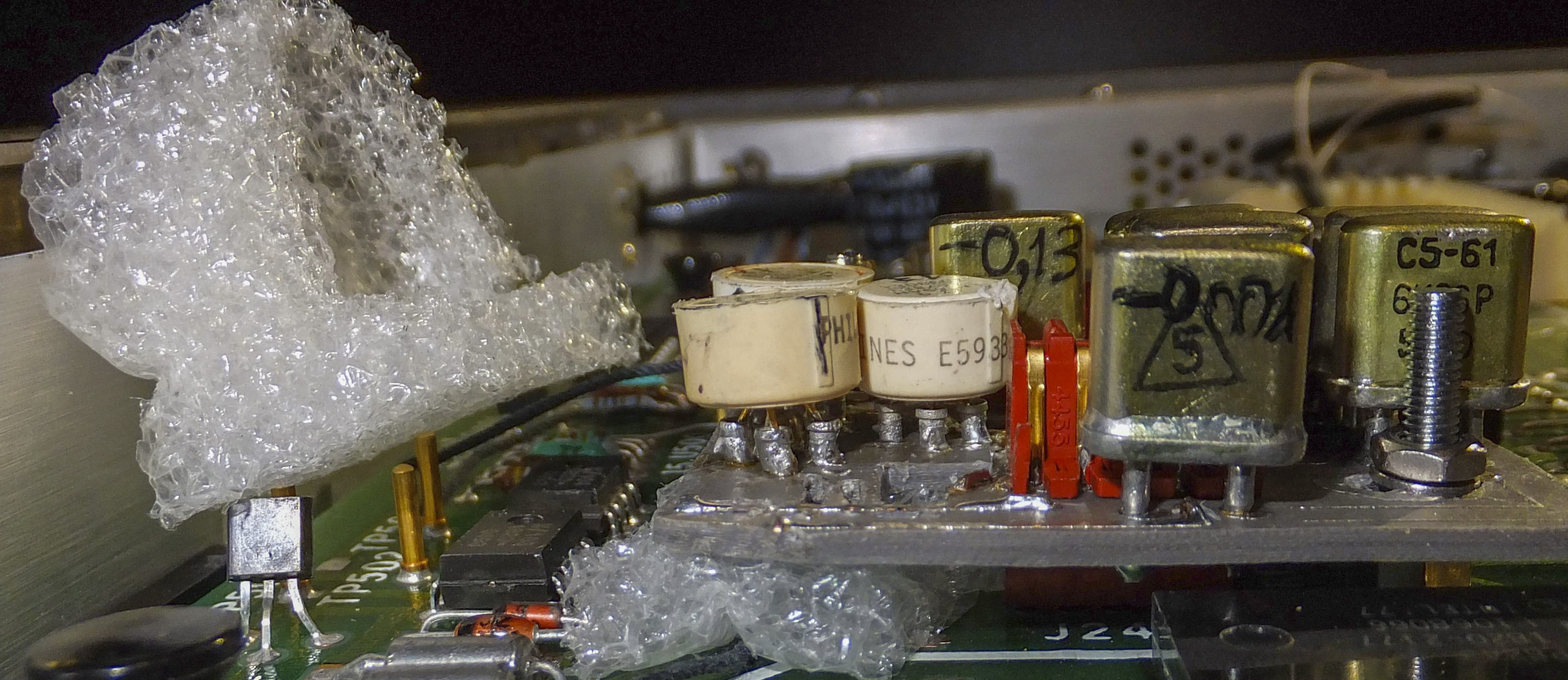
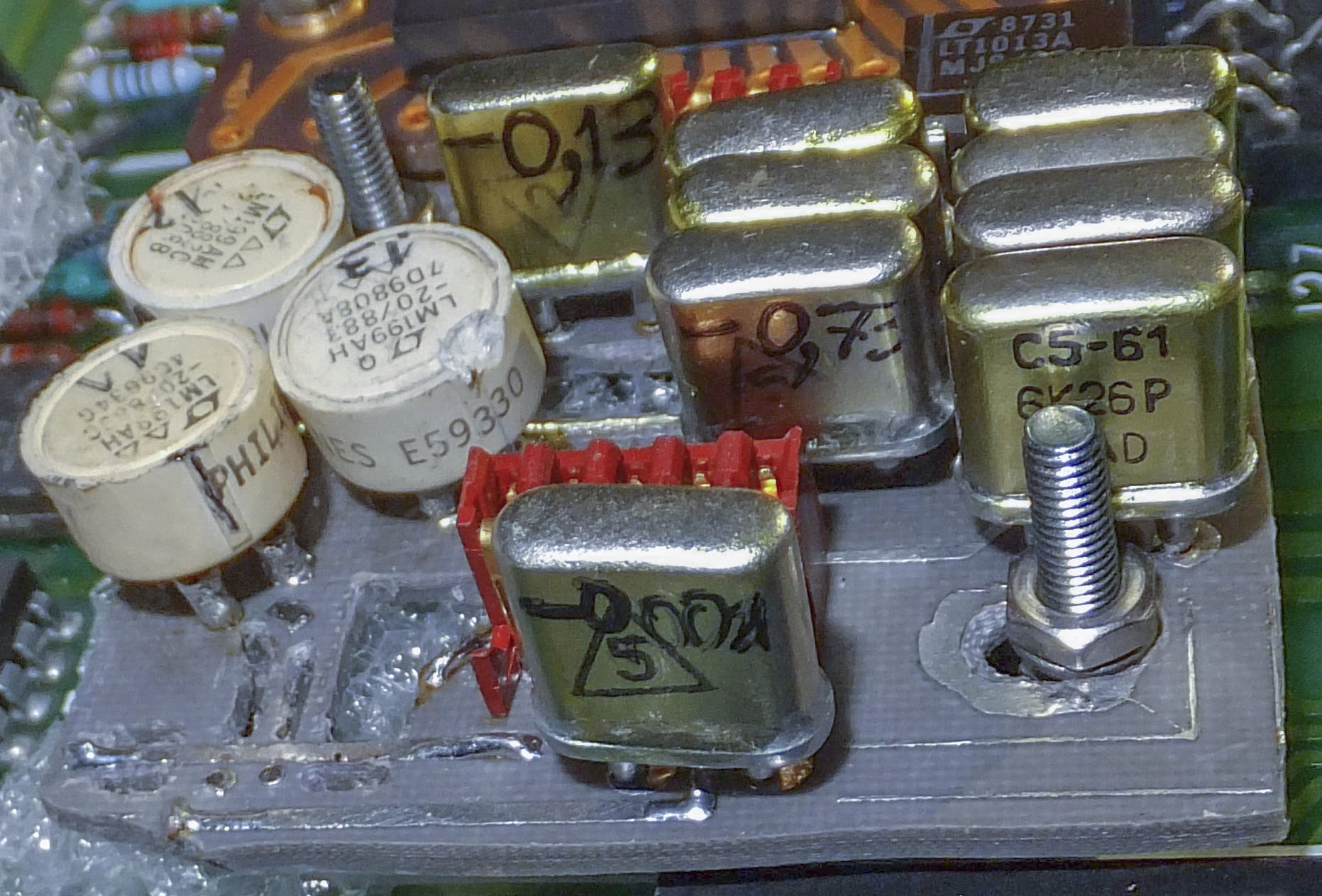
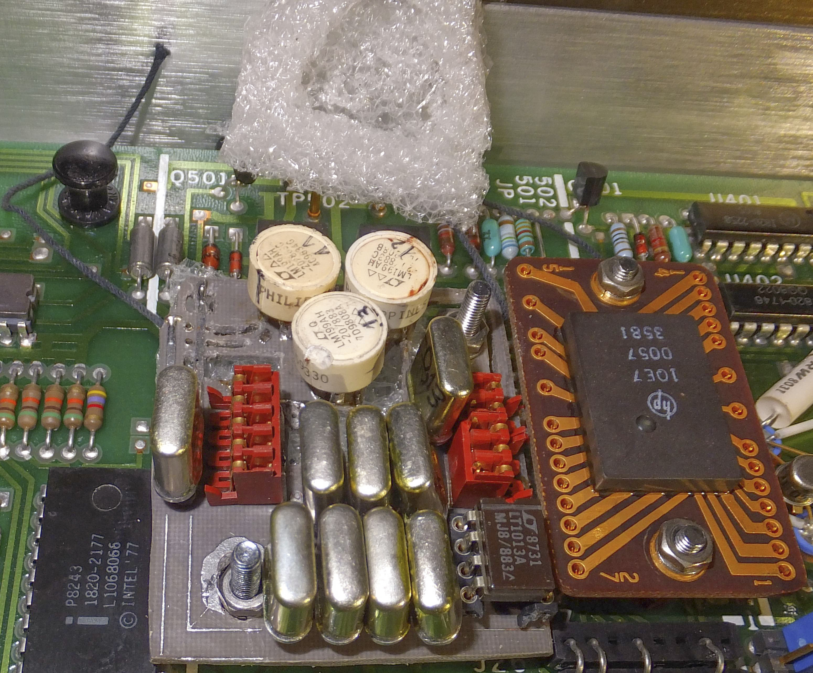
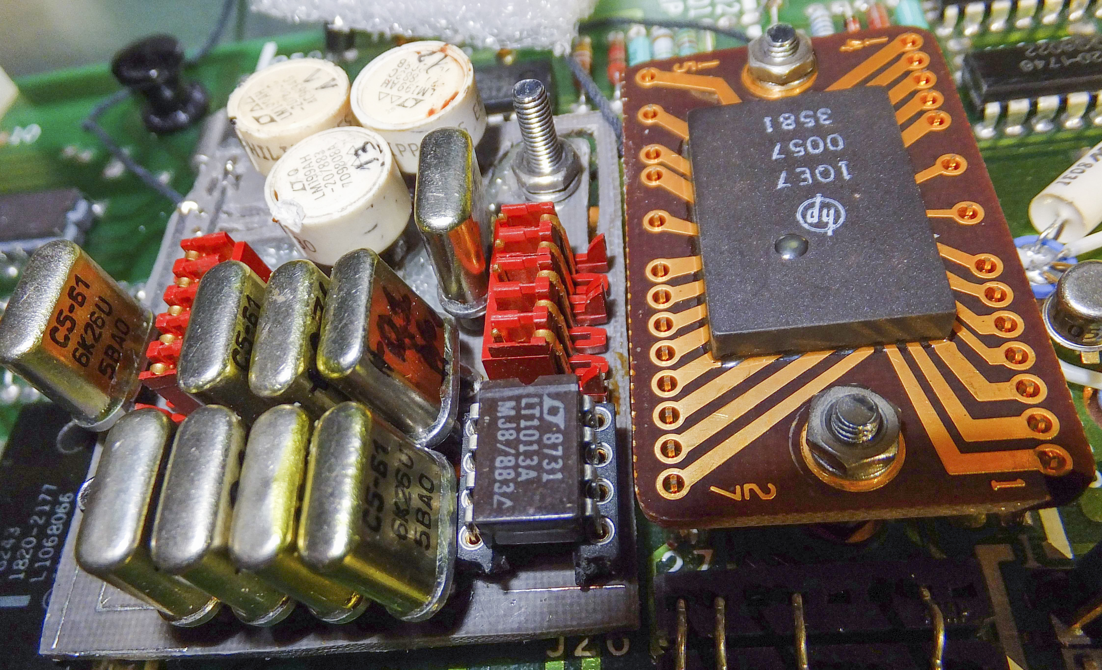
Decision was taken to modify original PCB around LM399 zener chip, leaving only space for PCB tracks. This approach will allow reducing thermal coupling between zener diode and circuit boards around, helping to reduce thermal power required to maintain temperatures.


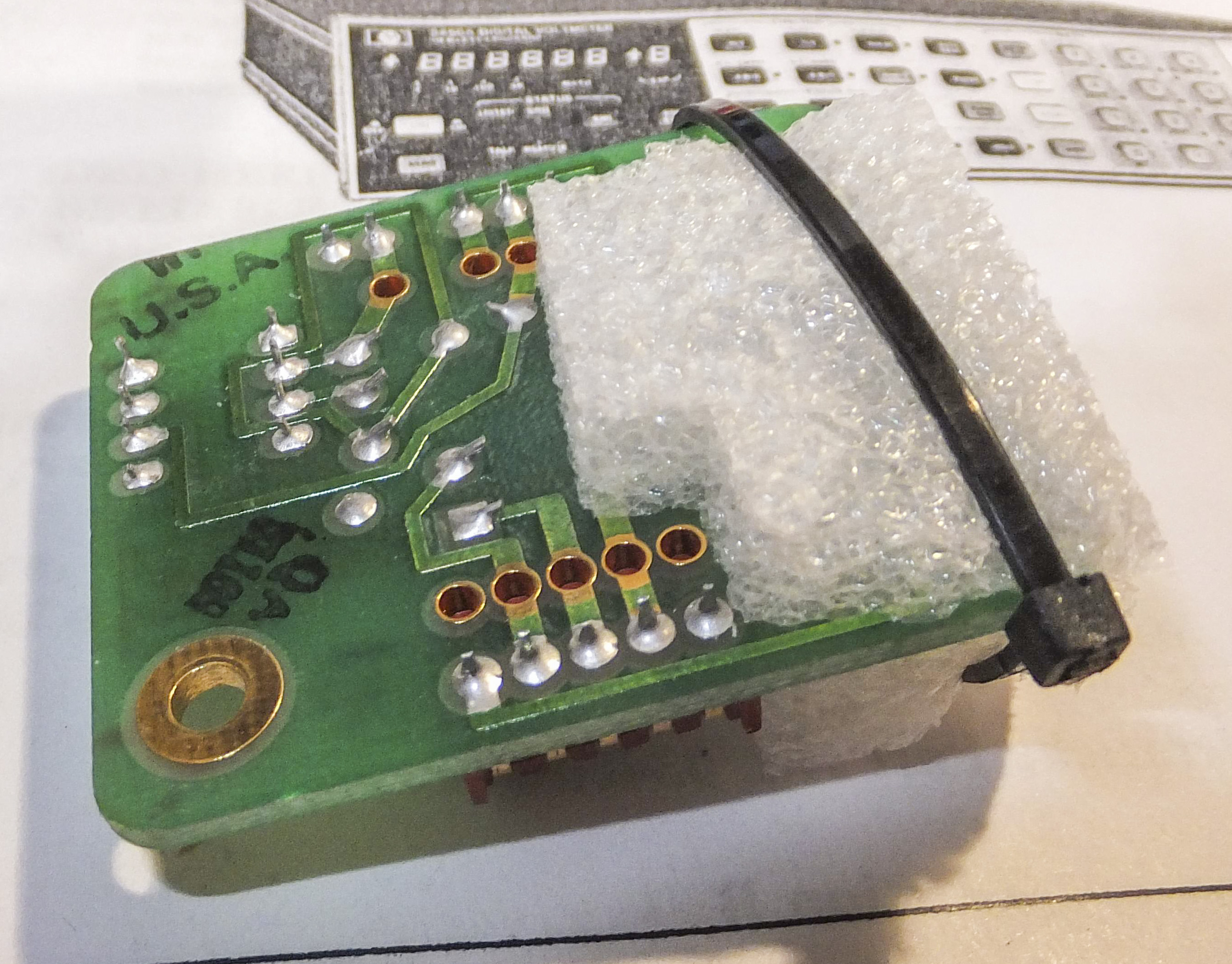

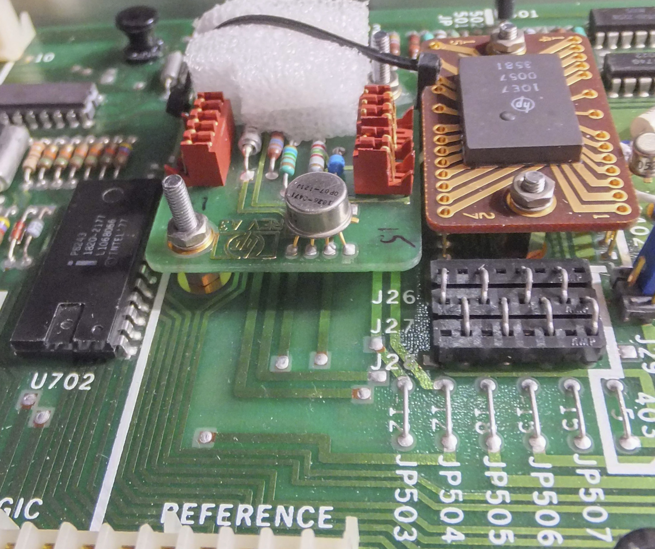
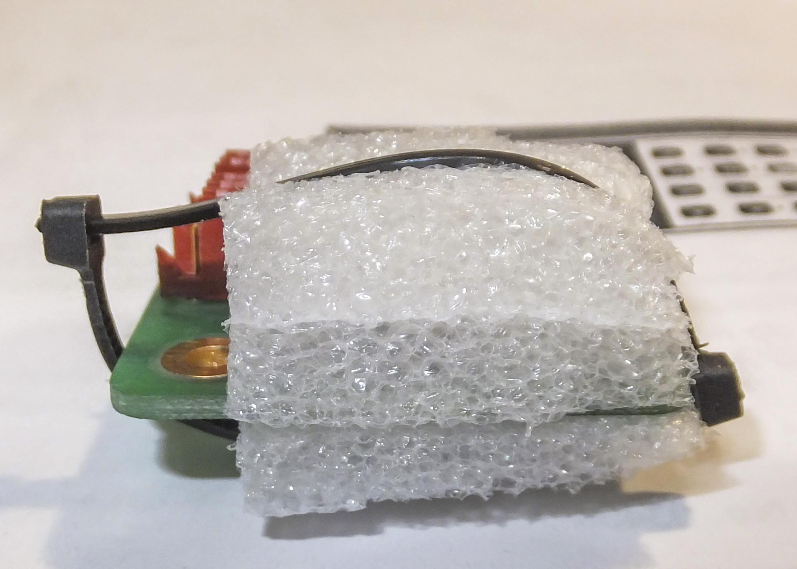
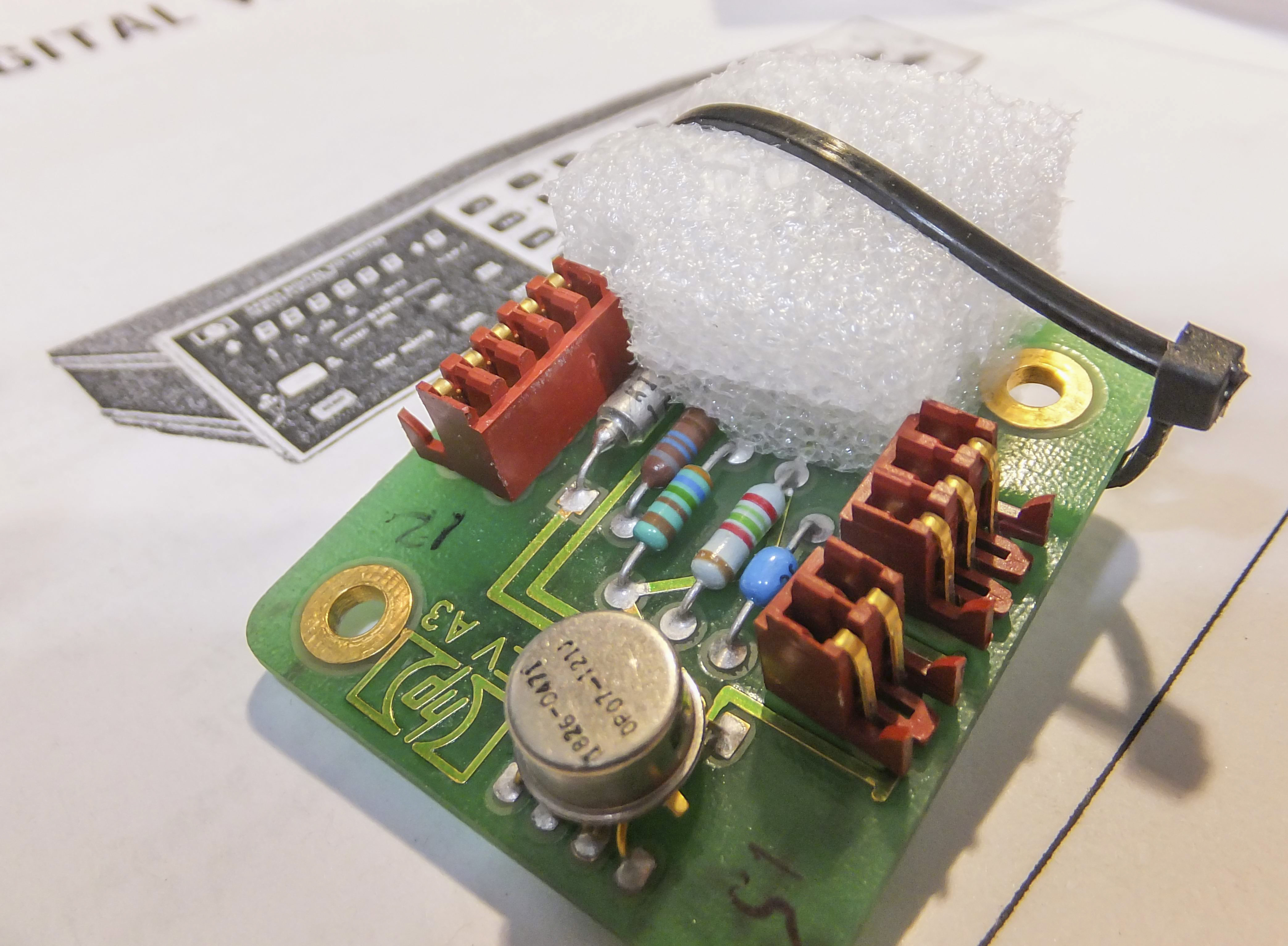
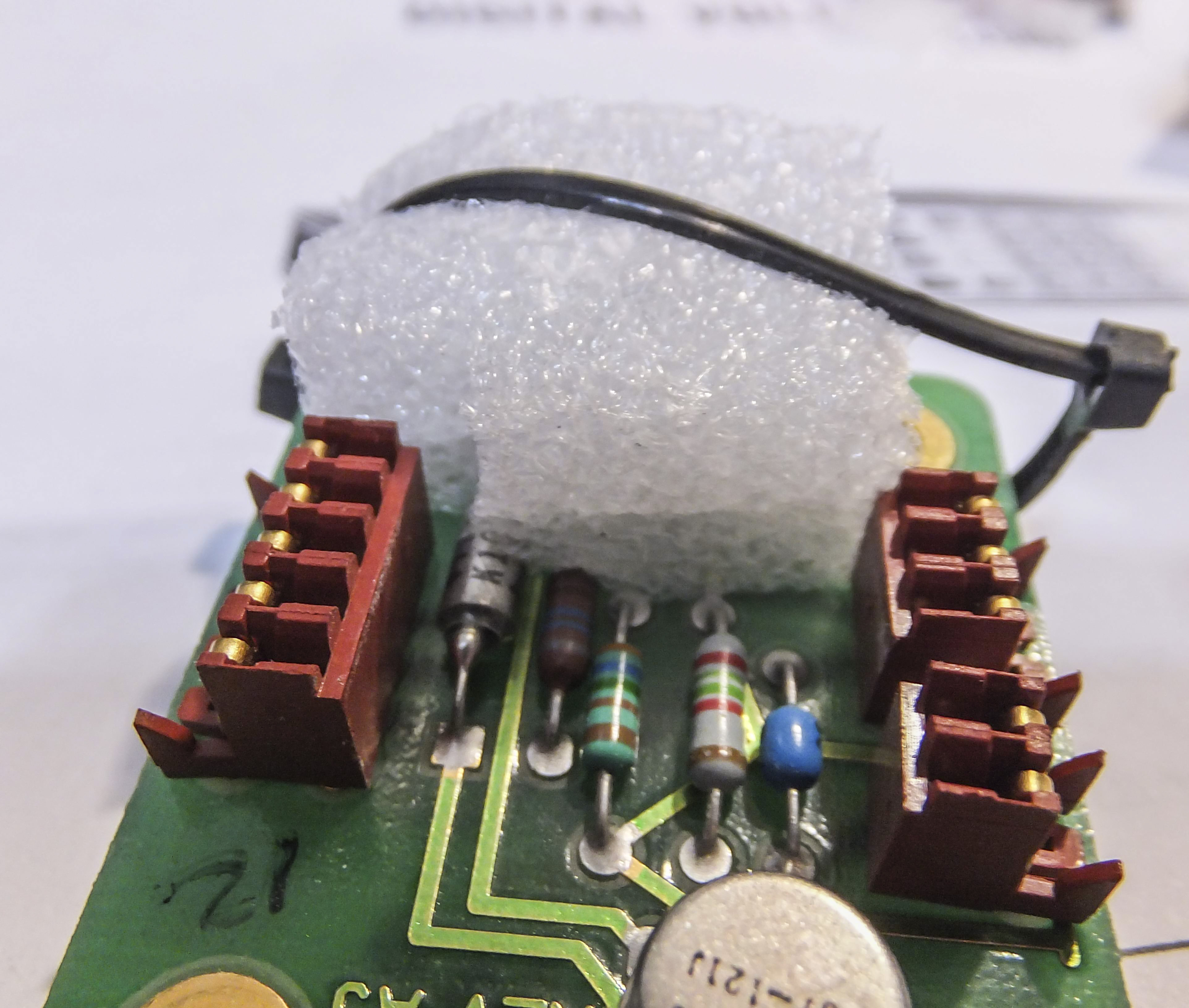

It’s critical to be extremely careful, not to track tiny traces around or damage components. To further isolate reference there were foam caps installed on top and bottom surfaces of reference board, like was shown on photographs. It’s best to fix these caps with simple fabric thread, instead of plastic coupler, as excessive pressure and mechanical force will cause extra stress to zener chip and output voltage will observe larger drifts.
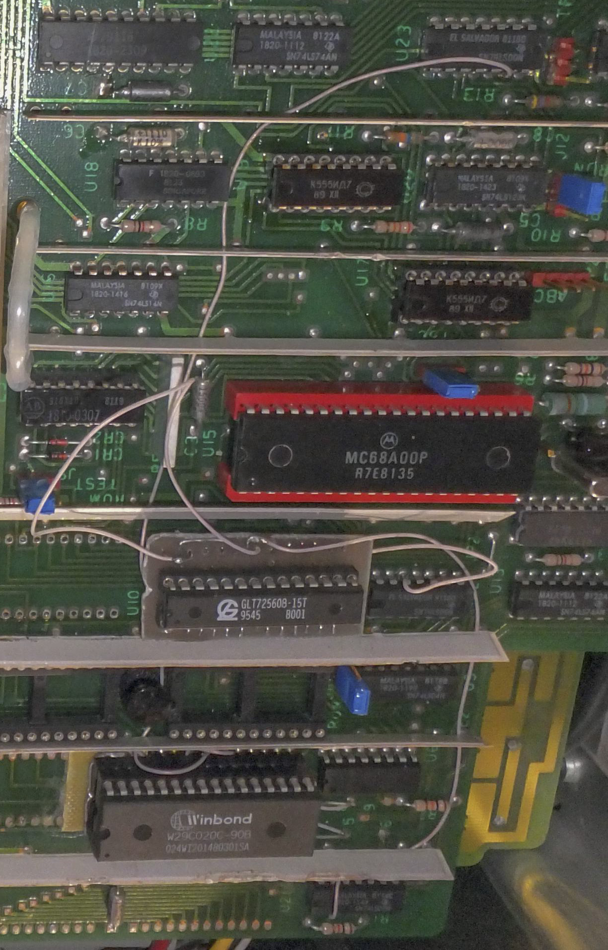
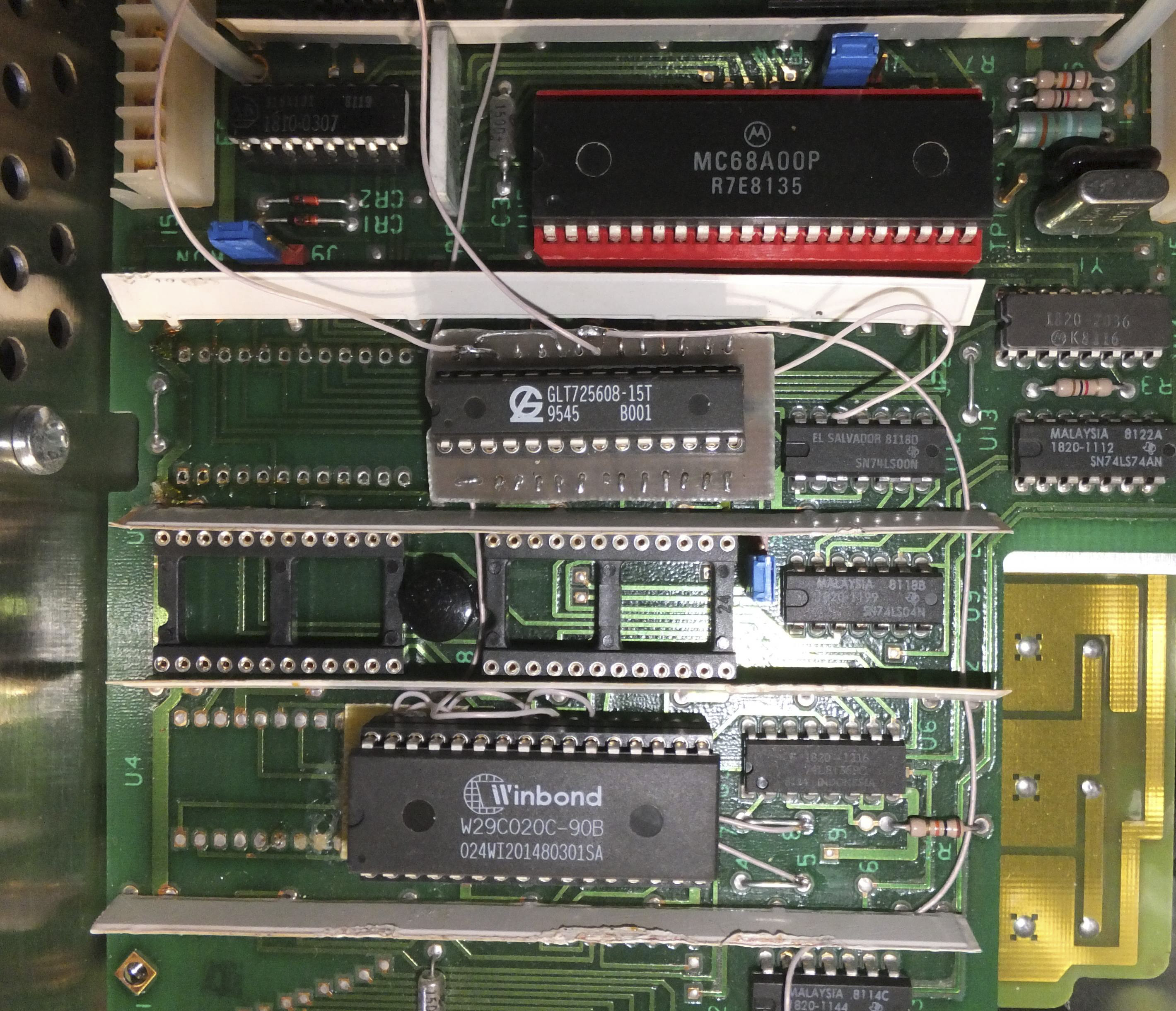
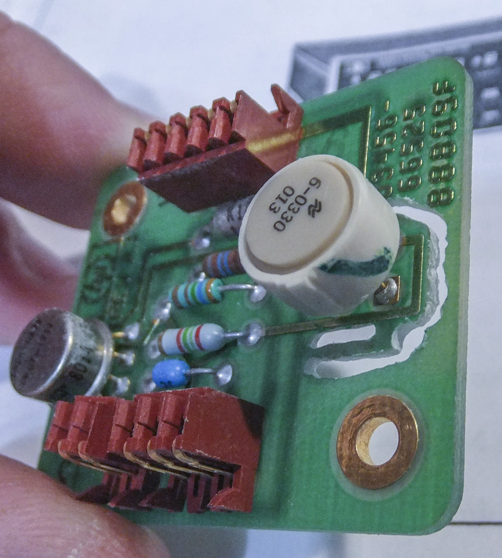
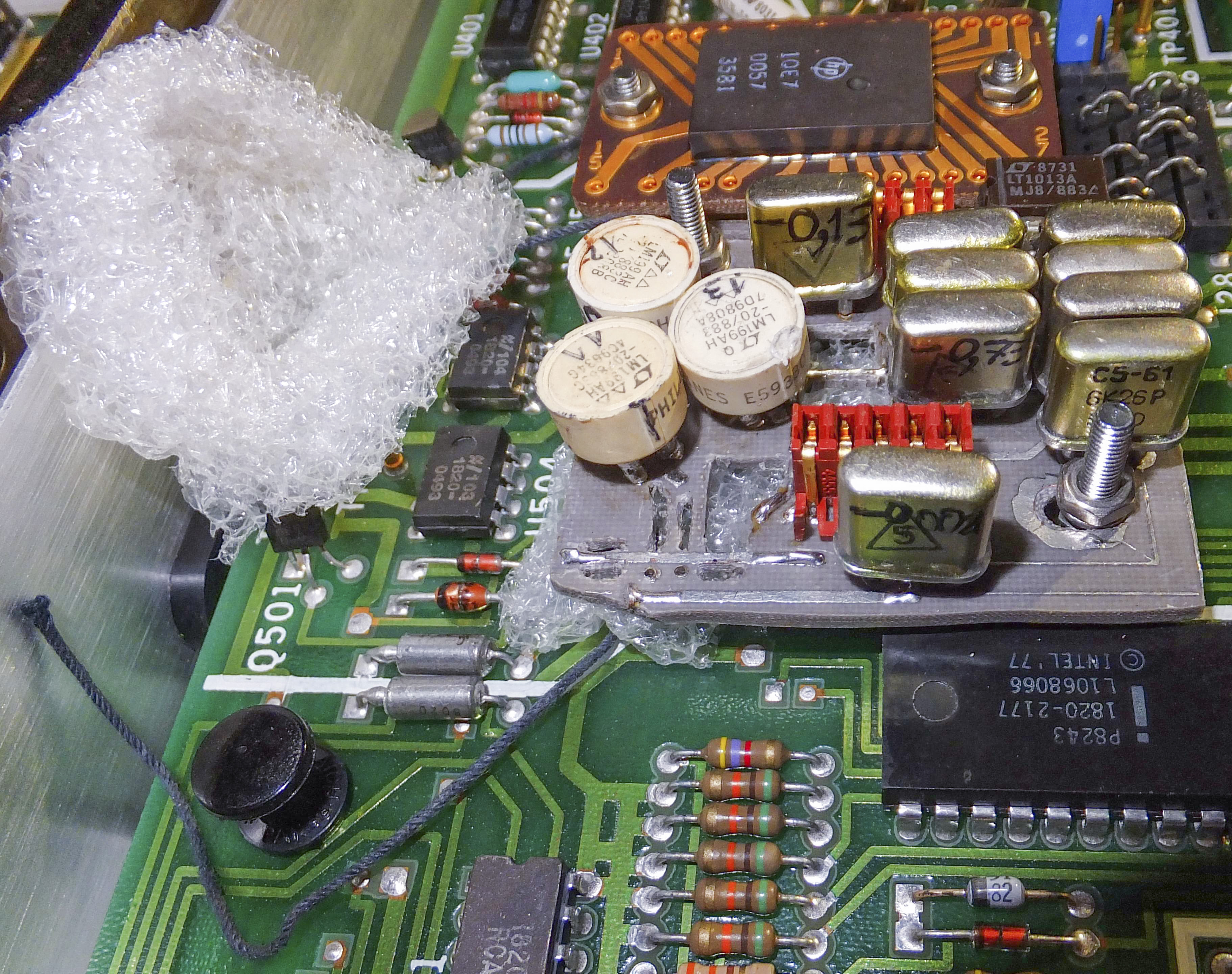
Application of second note from Mr. Dobkin, using multiple voltage reference zeners, was possible to perform just now, in progress of writing this article. Schematics of triple zener reference is shown below:
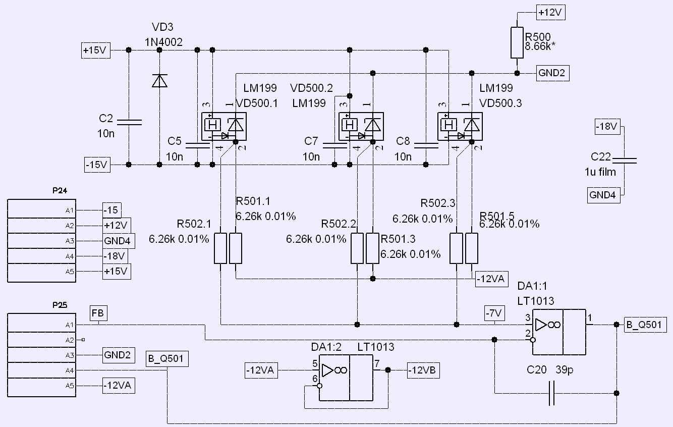
This circuit allow reducing thermal drift and output voltage noise by square root of three. Circuit was assembled on simple DIY PCB, which will replace original HP 03456-66525 module. Three LM199 (they were deliberately bought used, with old date of manufacture, to avoid initial aging effects) were grouped on one side of PCB, while resistors and operational amplifier LT1013 were populated on opposite side.
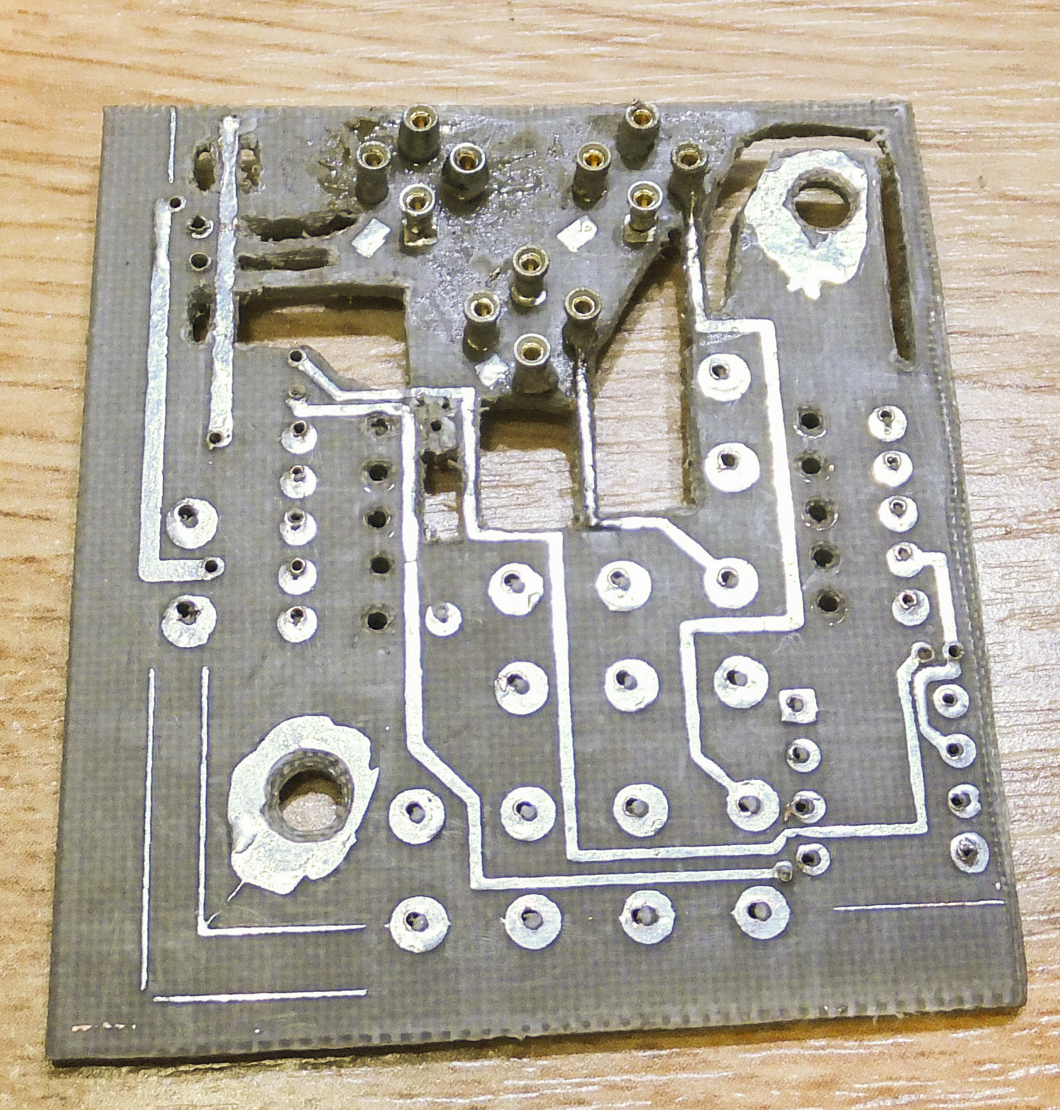

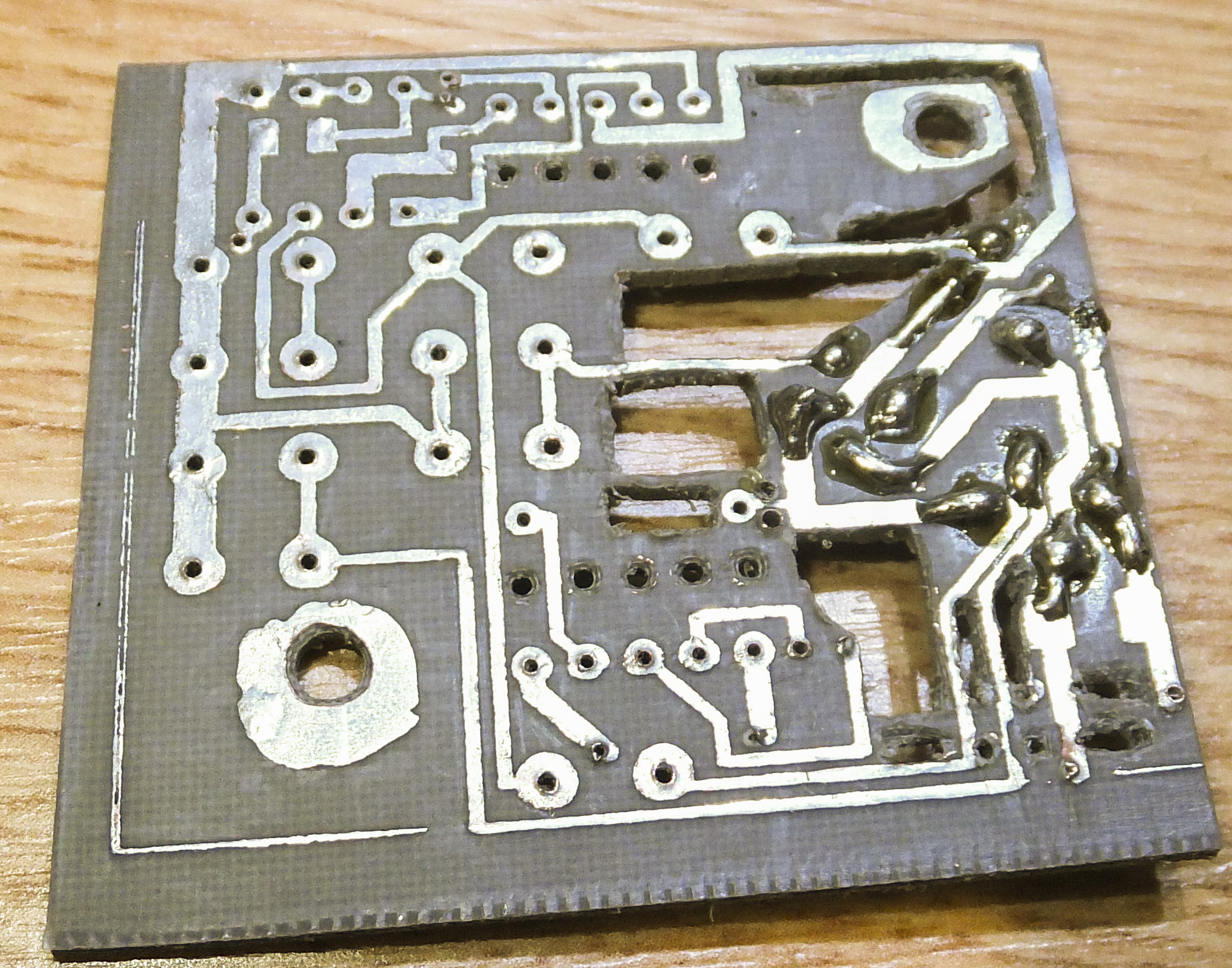

PCB cutouts were milled around LM199 zeners, and top and bottom sides were further isolated by foam caps, similar to previous approach with original voltage reference module.

Covers replacement
Missing outer cover was purchased on eBay, and inner shields were DIY manufactured. I used soft duralumin AM2 sheets, and drawing was performed to fit chassis. Metal cover thickness is around 1.5-1.6 mm, but I had only 2mm stock, so had to mill a bit around plastic locks to allow proper installation. Finished covers after few weeks of initial testing were darken using ferric chloride. This was targeted to reduce metal emission and improve thermal dissipation. Results are available for comparison: without inner shield covers temperature sensor was reading +6°C delta against ambient temperature. After installation shiny covers, this temperature was raised to +11°C. Blackened final shields allow dropping temperature difference back to +9°C.
Oscillator change for 50Hz mains
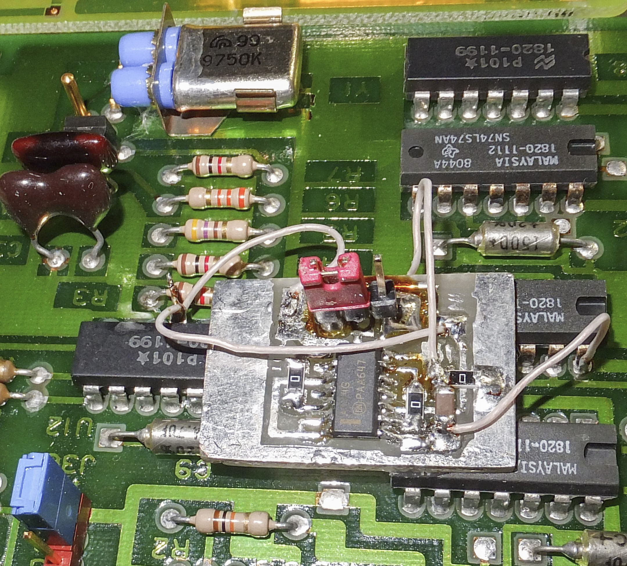
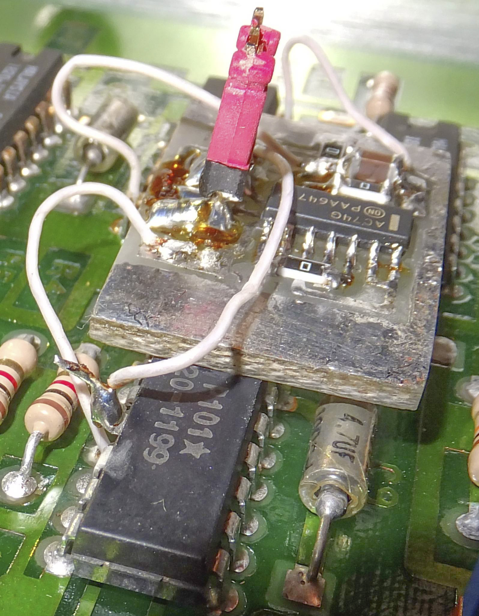
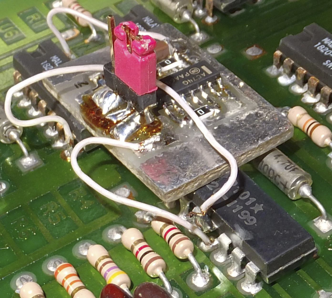
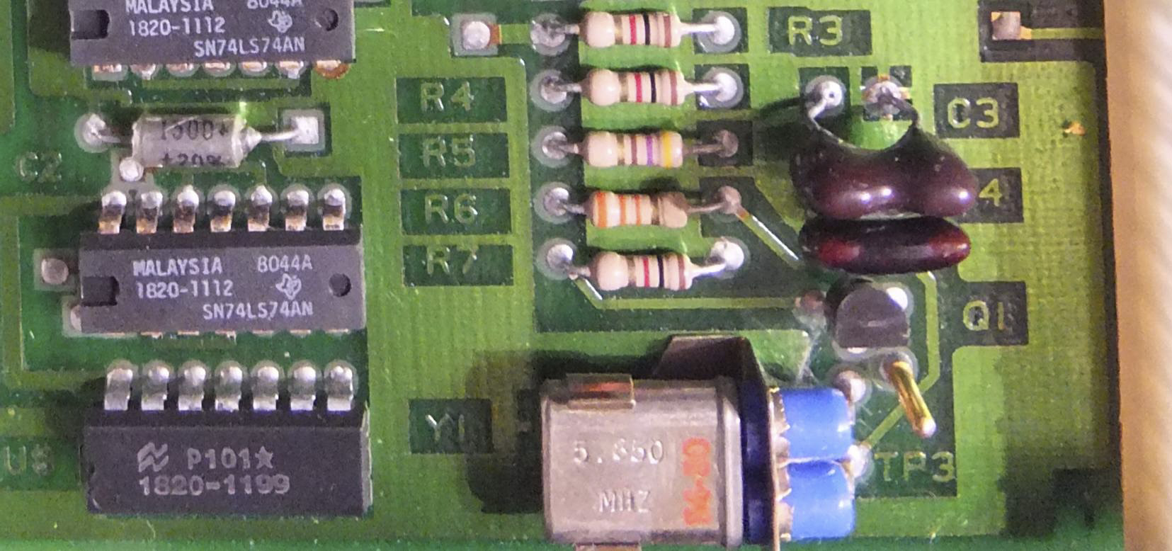
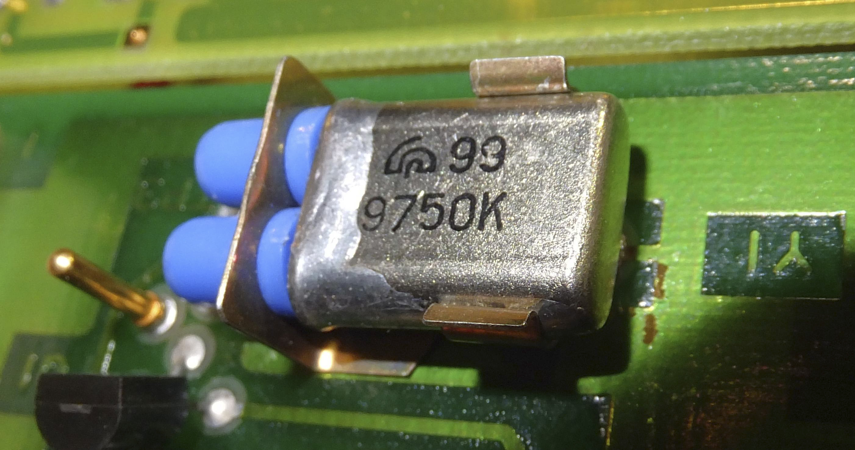
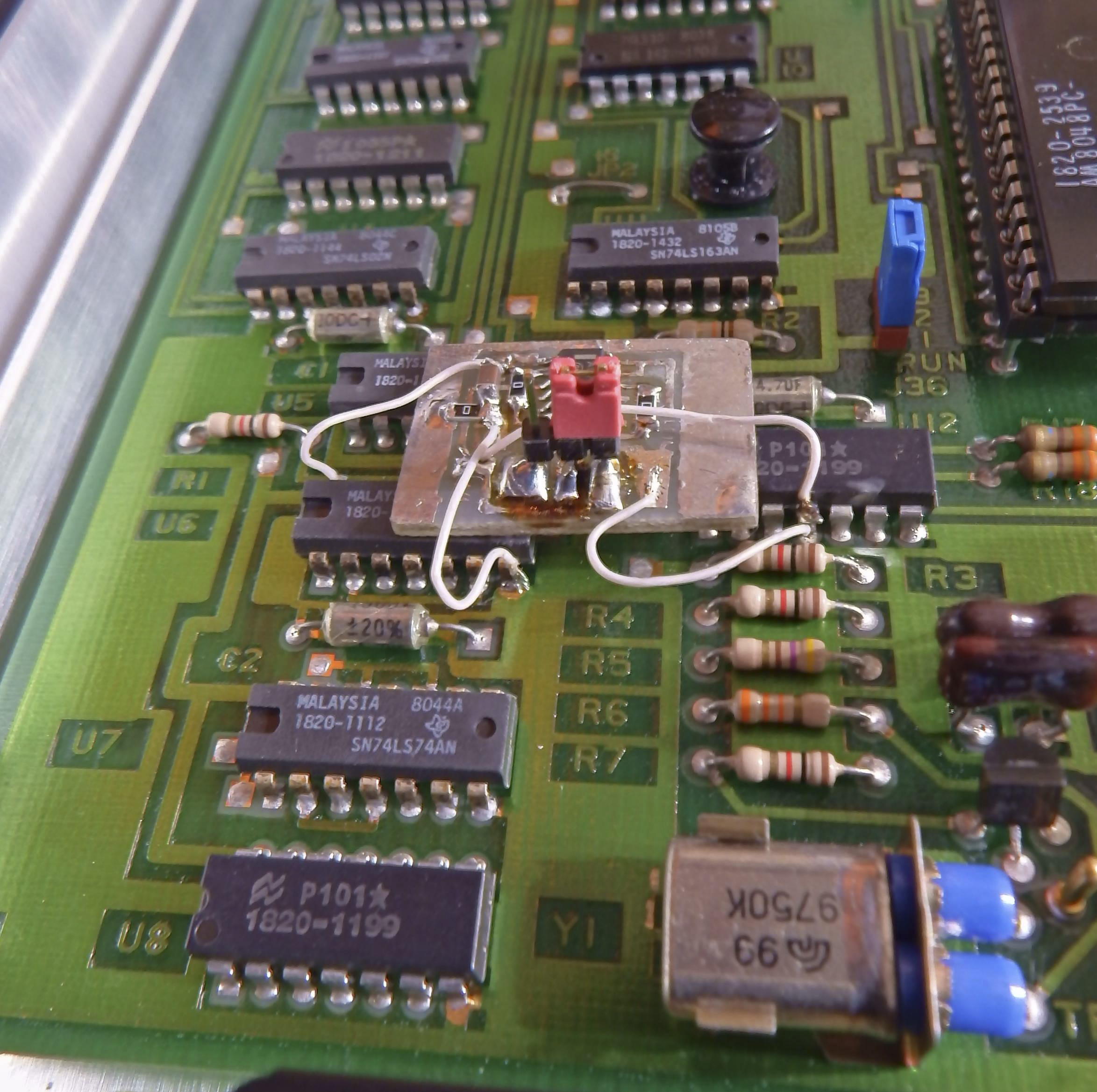
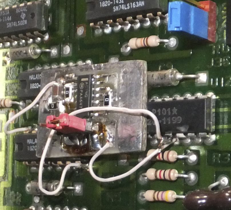
HP 3456A was designed to operate in USA, and tuned to work with 60Hz mains line frequency. Since here we have 50Hz mains, I’ll replace main oscillator to 4,875 MHz. I could not find this specific clock crystal, but doubled and quadruple quartz oscillators were available in local Quartz shop. I got one with similar case, such as this so original socket could be used.
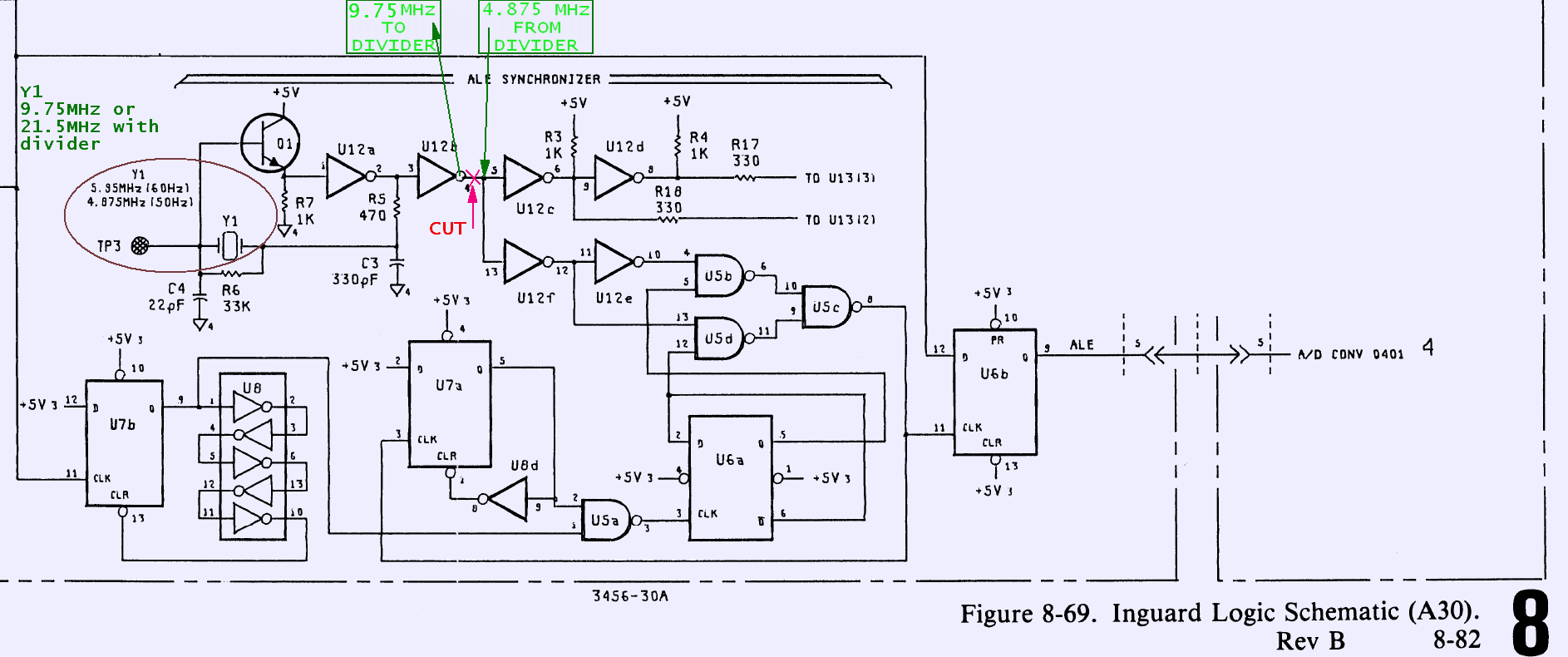
U12 pin 4 on A30 board was carefully desoldered and bent over PCB, so this output clock signal can enter clock division circuit. Divider output is routed back to free pin pad on A30 board. Clock divider is simple D-trigger based, usually posted on sites «for beginners». 7474 Logic chip was soldered on single-sided PCB, which fixed on top of U12 by glue.

Calibration
Final task of fixing meter – adjustment, or calibration, as it is usually referenced today. Lucky enough, HP 3456A calibration is rather simple, compared to multimeter such as HP3457A. Calibration sources and standards required are much less than amount of available ranges. For AC voltage only SINGLE source required, 1VAC with 1kHz frequency. For DC voltage sources of stable 0.1 V, 1 V, 10 V and 100 VDC are required. For resistance calibration only 1 kΩ, 10 kΩ, 100 kΩ, 1 MΩ and 10 MΩ are required. If exact transfer standards not available, DIY references and sources are acceptable for hobbyist level usage, if there is access to more accurate calibrated DMM during calibration period. This mean that we can supply same voltage to both calibrated control multimeter and 3456A under calibration to make values match. Make sure both instruments are being powered from same mains line socket, and very same connectors, cables are being used to reduce variables in signal path. This approach cannot be used for resistance calibration, but if stable resistors used, they can be measured first and then used for 3456A’s calibration.
In my case, HP 34401A was used as reference transfer standard DMM. For DCV, except 10V range, 34401A was used in DCV-DCV ratio mode, with stable 10V voltage reference with known voltage and temperature coefficient. Most important 10VDC range in 3456A was calibrated using direct connection to 10V voltage reference.
Direct voltage up to 11VDC was supplied by cheap calibrator EDC CR103J [12]. Higher voltage, 100VDC was generated by few series-connected zener references, and alternating 1 VAC @1kHz was generated from functional generator.
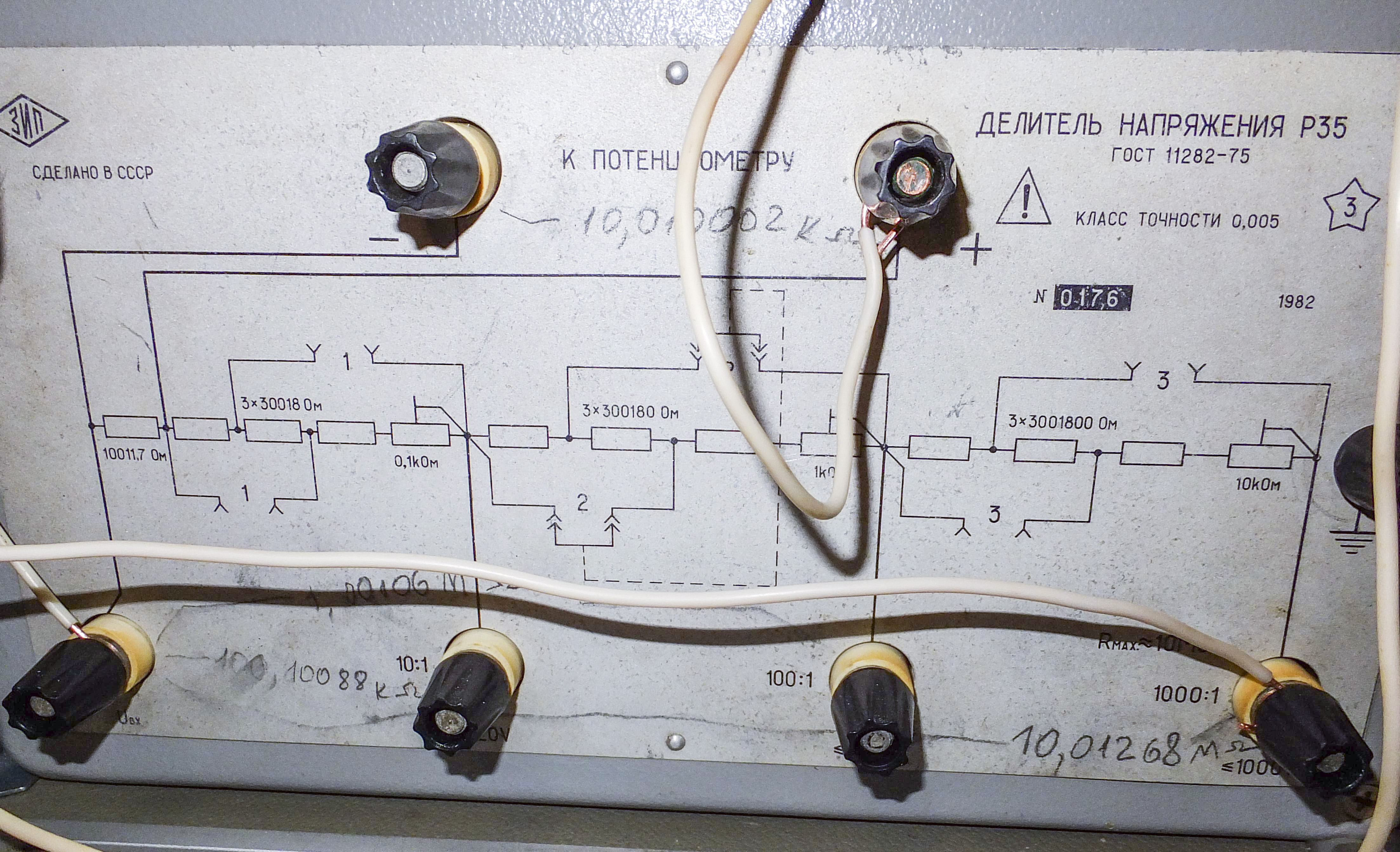
SSSR-made resistance decade box R4831 was used as resistance standard up to 100 k&Omega. 1 MΩ and 10 MΩ – were self-made statistical resistor networks, build with big quantity of S2-29 precision foil resistors. All calibration trim pots are available without meter disassembly, just by removing small front panel cover.


Good side of HP3456A – lack of NVRAM memories, and their battery cells. So calibration of 3456A cannot be lost due to longtime storage and battery depletion, unlike other instruments designed in 90’s.

Cover should be installed back after calibration operation to maintain stable thermal profile.
Results and performance
HP 3456A performance verification after calibration was showing much better stability than even newer 34401A, leave alone HP 3457A.
Tempco test for HP3456A
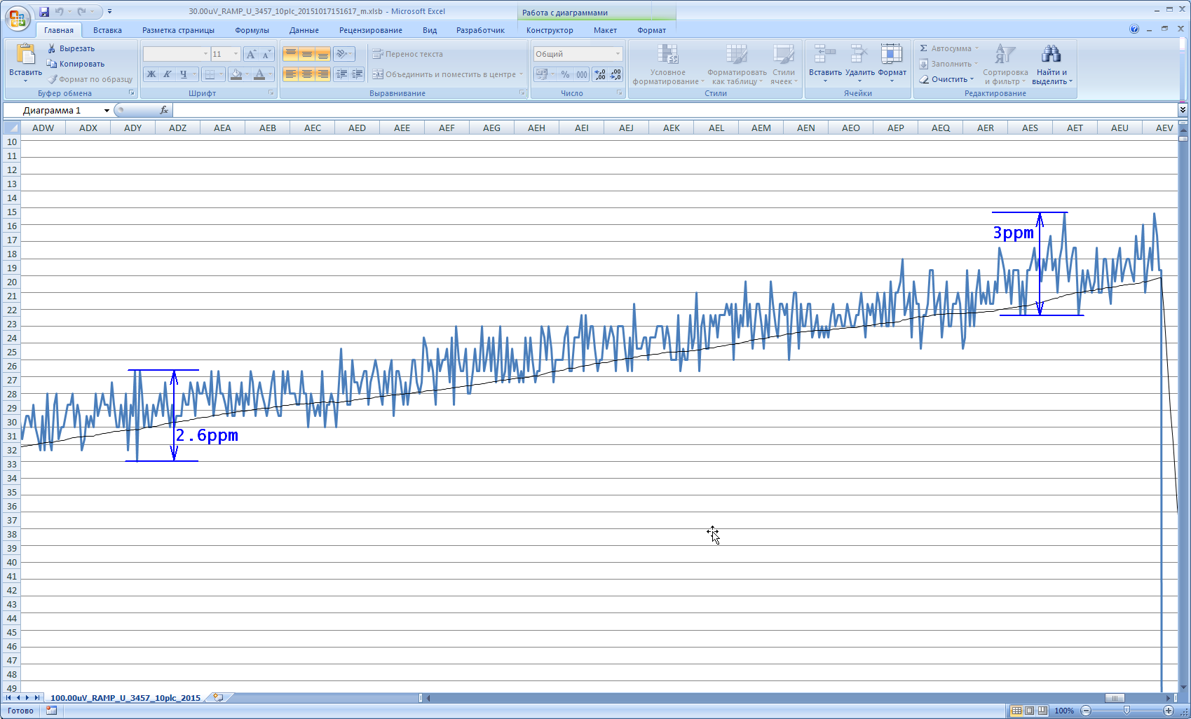
Improved original voltage reference board with caps fixe by strip demonstrated temperature stability at ~0,7 ppm/°С level.
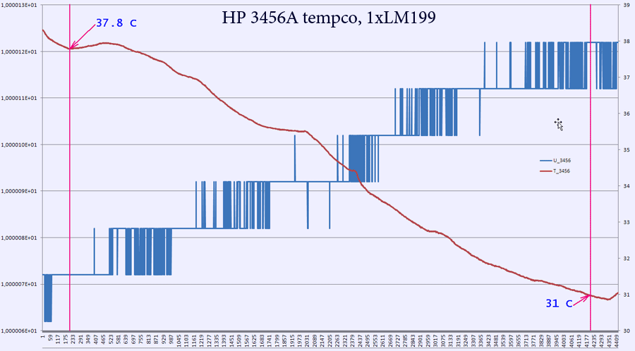
After improving isolation caps to avoid mechanical stress on voltage reference temperature stability improved to ~0.35 ppm/°C.
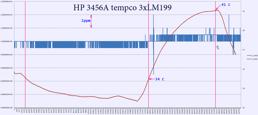
But most of benefit was achieved with our DIY triple LM199 module, providing 0,15ppm/°С temperature coefficient, which is good result for old 6½-digit DMM after repairs!
A/D linearity & noise test
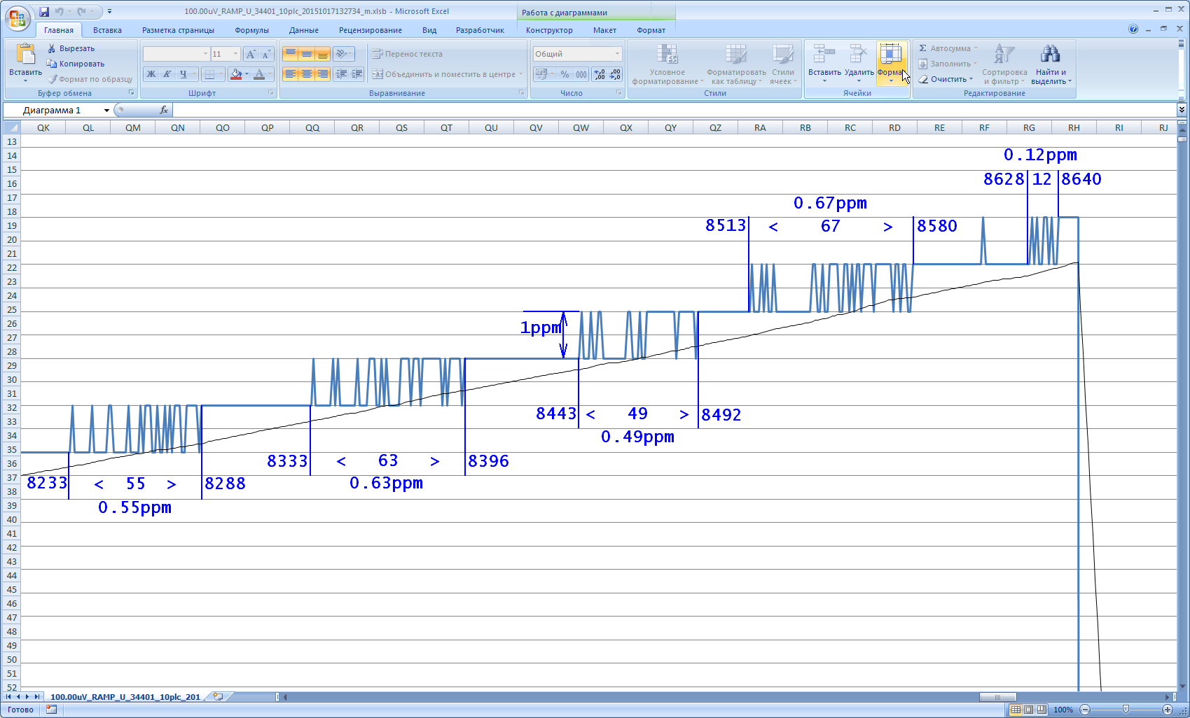
High-end Kelvin-Varley Divider or precision calibrator are required to measure and characterize linearity of precision A/Ds, like one used in this 6½-digit instrument, but I had no access to any of that expensive stuff. So plan B was to use simple generator of small scale sawtooth-signal, in range of 100 ppm around zero, so estimation about A/D noise and differential linearity could be made.
HP3456A in 6½-digit mode at 10 PLC is able to perform measurements with 2.5Hz speed, so I used 500ms timing in GPIB measurement. If we want to get 100 samples with 1ppm voltage differential this would take 50 seconds. For 100 ppm we will need 5000 seconds. Remember this value.
As sawtooth generator I used function source HP3325A in RAMP+ mode. Voltage output amplitude was set to highest value of most accurate range, which is 10V for HP3456A and HP34401A, and 3V for HP3457A. Now, recalling our time needed for 100 ppm span , we can calculate required frequency such as 1/5000sec=0,0002 Hz. Offsets are not being used, just set to zero, to avoid any unwanted instability in output. Generator’s output loaded with 50 &Omega resistor to ensure proper source operation.

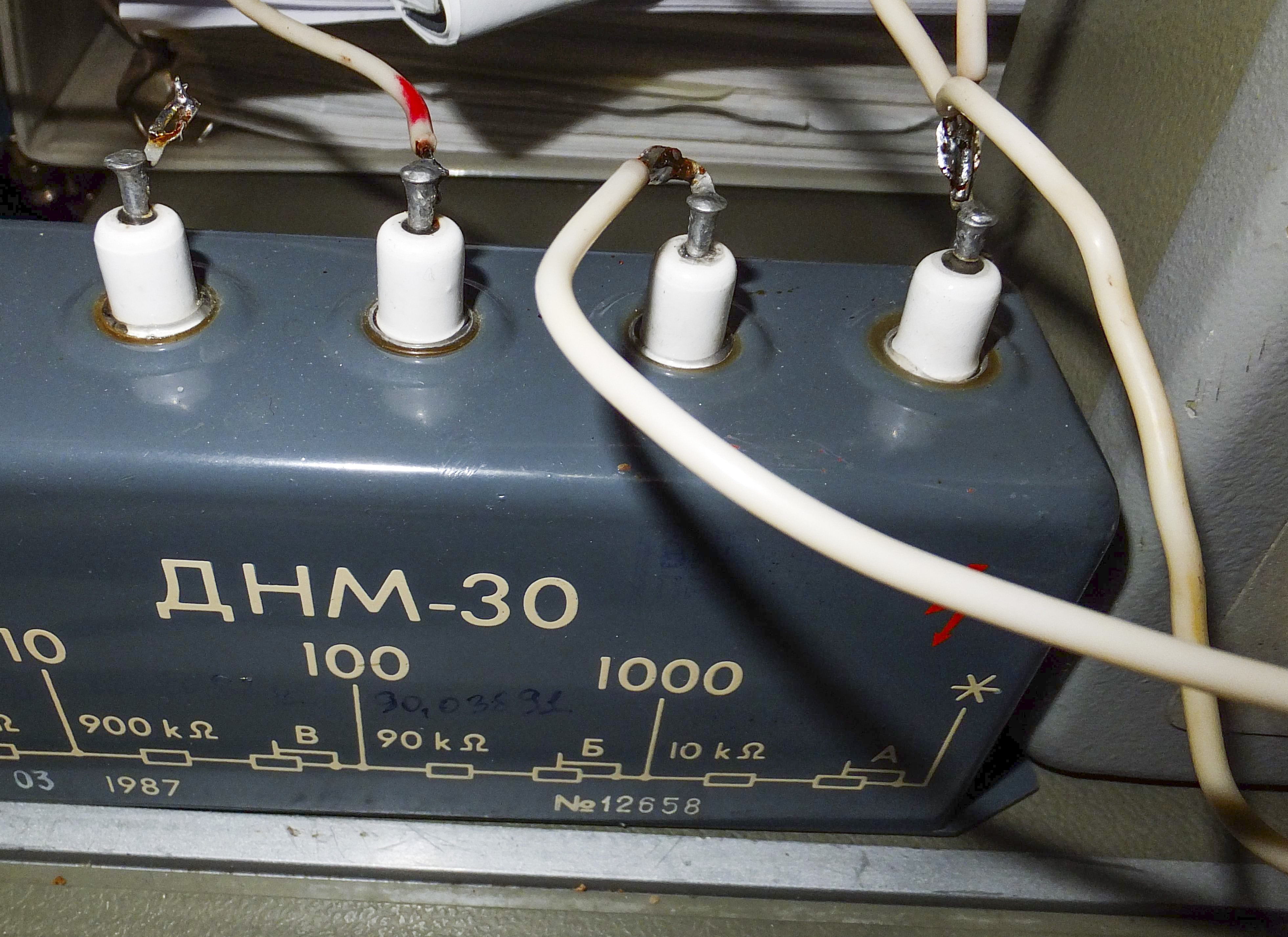
Divider 10000:1 was used to get signal with maximum range about 100 ppm. It was built around two resistive SSSR-made dividers, DNM-30 to divide 10:1 and similar R35 divides further 1000 times more. All connections are made by clean single-strand copper wire to reduce effects of thermal EMF.
Output of R35 divider was supplied to multimeters under test (HP3456A, HP34401A or HP3457A), data from which was captured to PC via GPIB->USB PROLOGIX interface. Simple Terminal program was used to capture, setup and store data. Further processing, analysis and graphing was performed in Excel.
All meters were configured with settings:
- NDIG: 6 (6½-digit mode);
- Manually fixed 10 VDC range (3 VDC for HP3457A);
- Integration time 10 PLC;
- Autozero: ON;
- Filter: OFF;
- Trigger: SINGLE (single conversion, except HP3457A, which was measuring continuously).
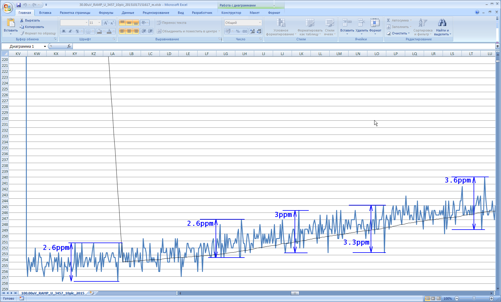
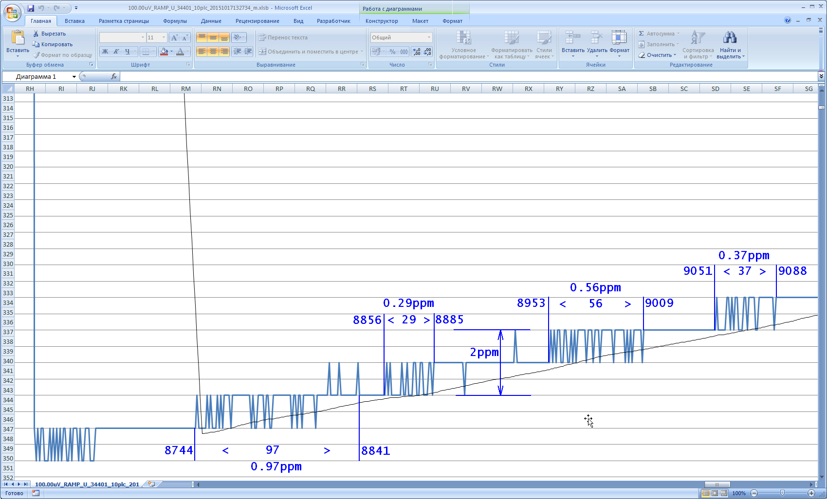
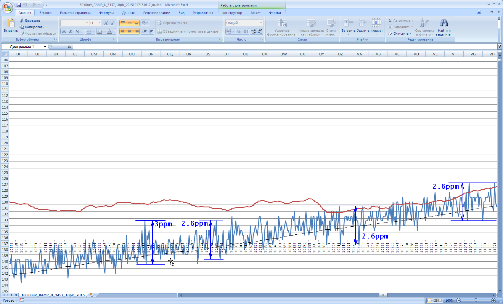
All data shown below in clickable graphs, and details available for download in Excel-table. Blue graph is measured voltage, black line is averaged value out of 100 samples and brown line is internal (or external for HP3457A) temperature.
| HP 3456A | HP 3457A | HP 34401A | |
| Performance at -50 ppm | 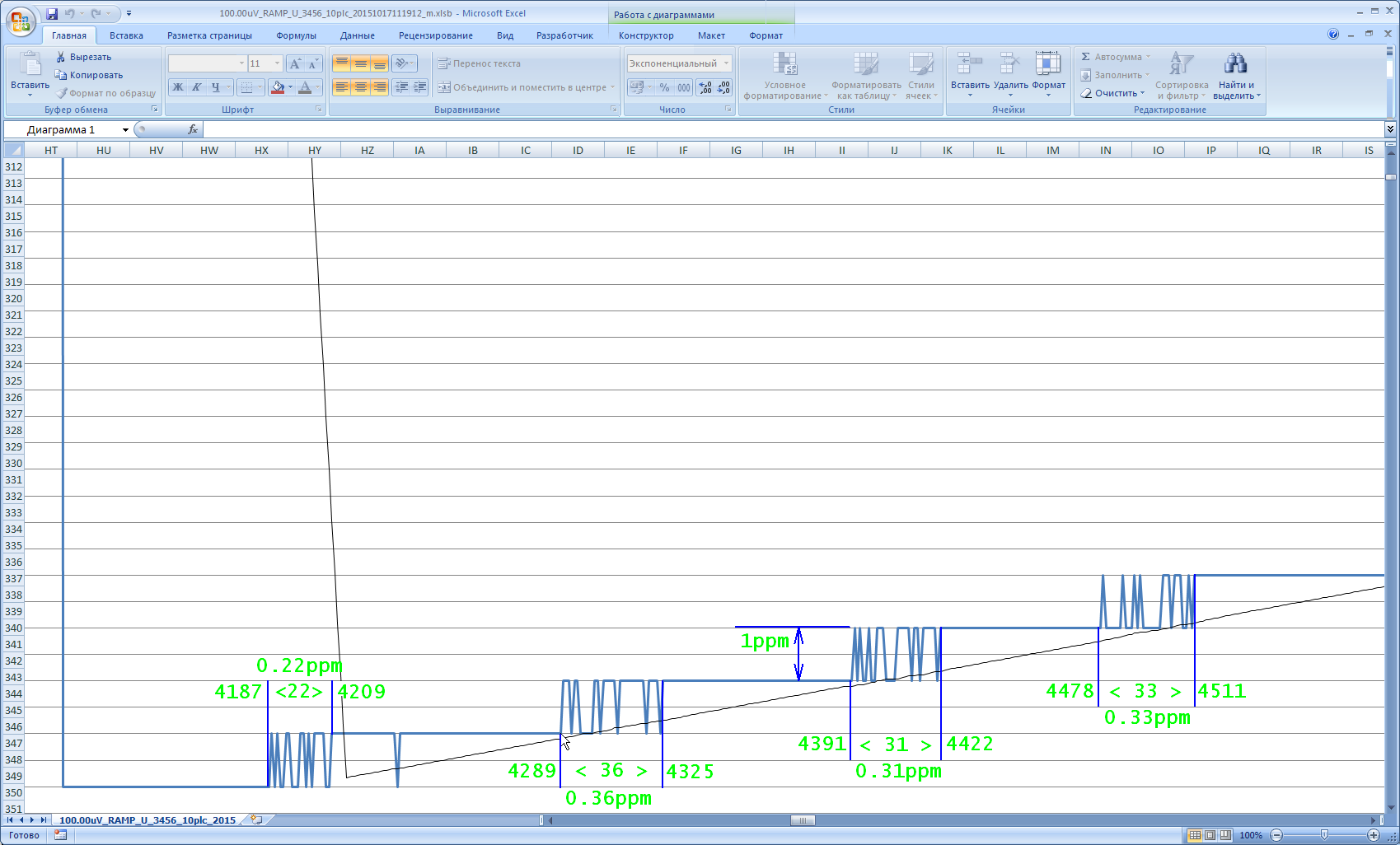 |
 |
 |
| Zero scale performance | 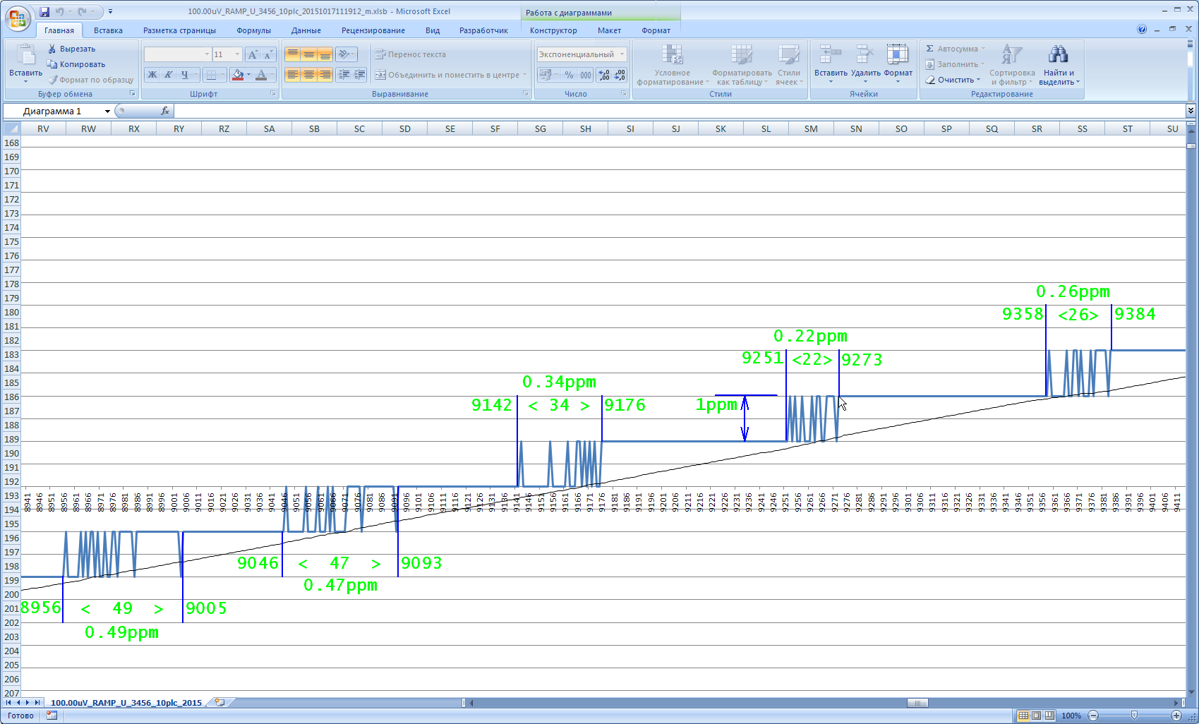 |
 |
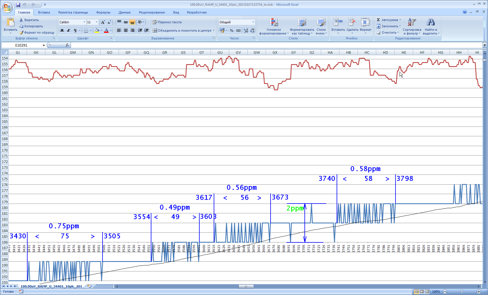 |
| Performance at +50 ppm | 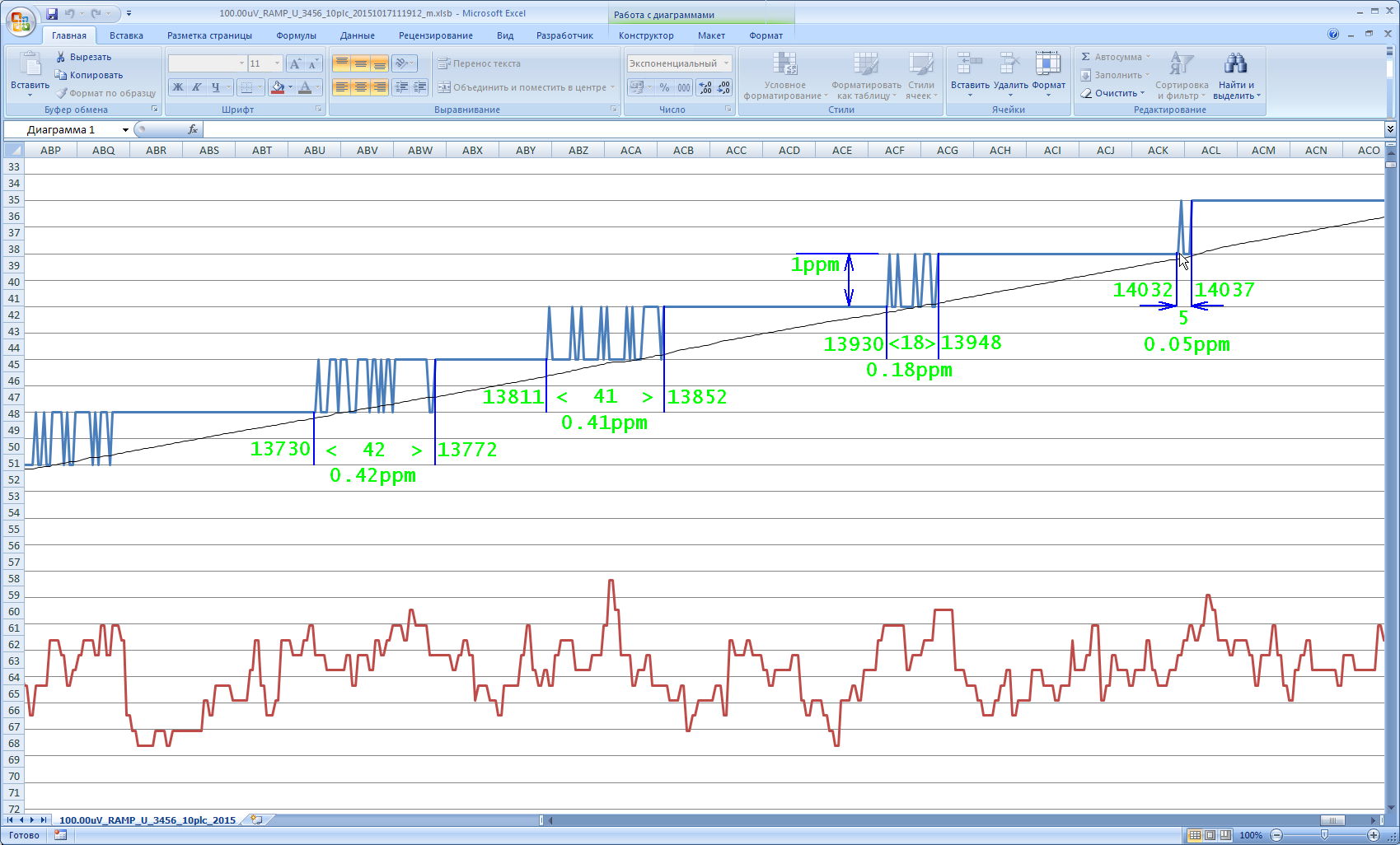 |
 |
 |
Since HP34401A provides 7 digits over GPIB interface, all results were rounded up to 6 digits using usual math averaging. It was not performed for HP 3457A data, as it was not clear how to average to 3. That’s why data log from 3457A have samples in multiplies of 0,333 or 0,666 ppm.
HP3456A noise levels was within 0.05 ppm … 0.49 ppm range, in average about 0.35 ppm ±0.07 ppm.
HP34401A noise levels was within 0.12 ppm … 0.97 ppm range, in average about 0.55 ppm ±0.25 ppm.
HP3457A noise levels are much higher, over 1 ppm. According to peak-peak measurements, noise level was within 1-3 ppm, with average 2 ppm ±0.6 ppm.
Summary
As we can see, most stable is our modified HP3456A, following with much newer HP34401A, and outsider HP3457A. In case of 3457A, it’s likely due to additional amplification with gain 3.33 in 3457A, while other instruments had direct measurement path. 3457A is even more strange in higher voltage range, such as 30VDC, as it goes to 100:1 high-voltage divider first, and then result get amplified with gain 3.33.
Another detail worth mentioning, HP34401A and HP3457A multimeters are able to provide actual 7½-digit data via GPIB-interface, while our modified, more stable 3456A cannot provide that extra digit of resolution. Would be great to have free digit, since we manage to improve stability and performance of meter, adding sense for extra resolution.
Would like to note, that all measurements were done in hobbyist environment, without expensive metrology-grade instrumentation, and likely affected by external interference, temperature variations and such. Only single units were tested, which were not had recent calibration. So these results are indicative purpose only, and may differ of your results or other results published elsewhere.
If you have any suggestions or question regarding this meter or modifications, please let us know in comments.
TEKTRON 22.10.2015
Projects like this are born from passion and a desire to share how things work. Education is the foundation of a healthy society - especially important in today's volatile world. xDevs began as a personal project notepad in Kherson, Ukraine back in 2008 and has grown with support of passionate readers just like you. There are no (and never will be) any ads, sponsors or shareholders behind xDevs.com, just a commitment to inspire and help learning. If you are in a position to help others like us, please consider supporting xDevs.com’s home-country Ukraine in its defense of freedom to speak, freedom to live in peace and freedom to choose their way. You can use official site to support Ukraine – United24 or Help99. Every cent counts.
Modified: Nov. 24, 2015, 2:32 a.m.
References
- The Boat Anchor Manual Archive : /hp/3456a/
- KO4BB manuals : 3456A Manual
- Forum discussion : HP 3456A multimeter ROMS gone bad
- Volt-nut mail list : A history of the HP 3456A
- GLT725608/08L SRAM Datasheet
- EEVBlog : HP3456a service notes, for owners info!
- LMx35, LMx35A Precision Temperature Sensors
- MX29F002/002N Datasheet
- LM199/LM299/LM399 Precision Reference
- Kurt manuals : EDC CR103J Operation manual
- Resistance decade box R4831
- KO4BB : HP 3325A Operation manual
- Radiokot.ru : Цифровой мультиметр HP 3456A (Russian)
- EEVBlog : HP 3456A DVM CPU Board Rev-B ROM replacement
- EEVBlog : HP 3456A repair LM201 replacement
- EEVBlog : HP 3456A fixes and repair thread