Contents
- Intro
- Disclaimer
- Manuals and documentation
- Project concept and workflow
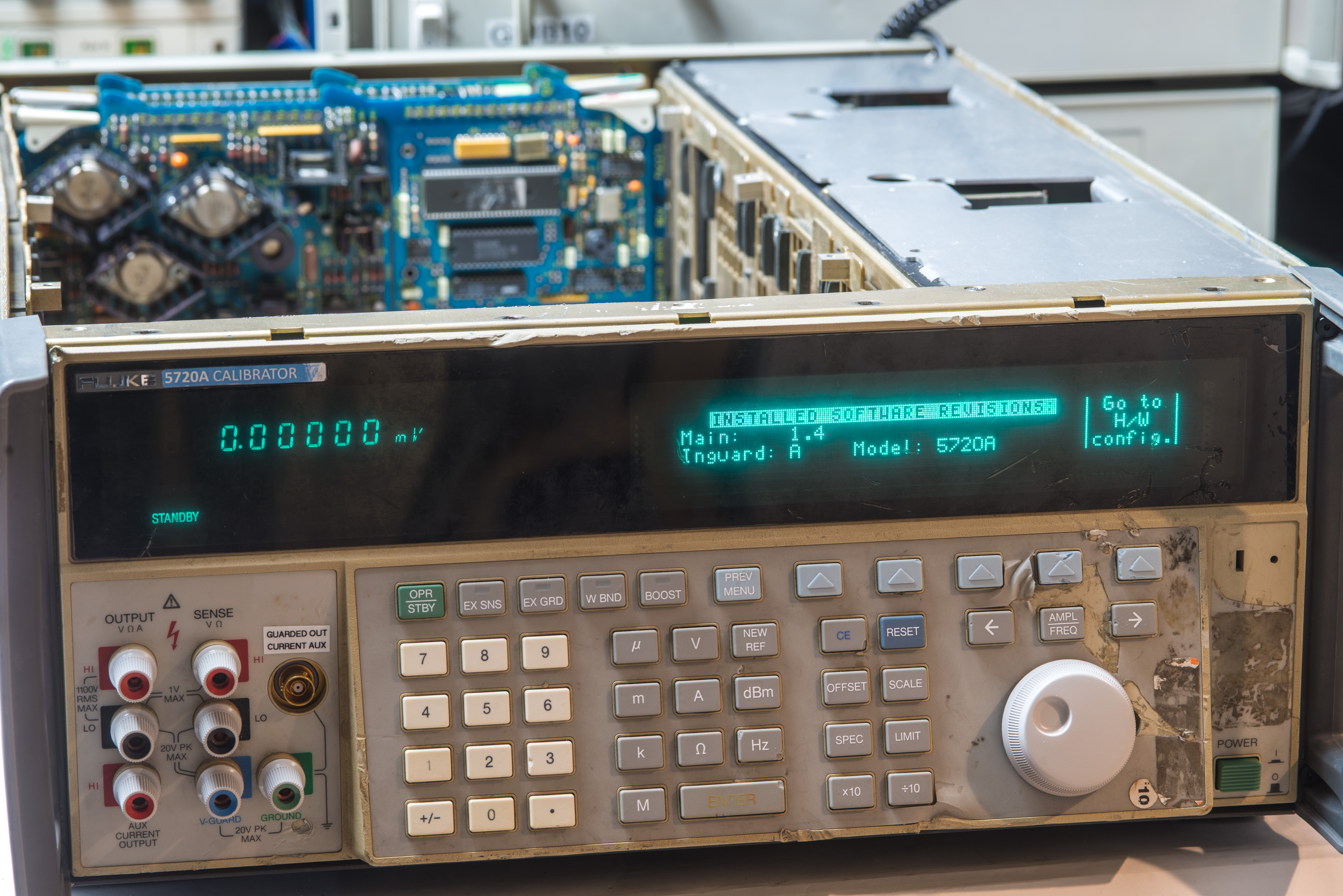
- Modularity and 5700A/5720A flexible diagnostics
- Fluke 5700 ‘C’ Hulk-III build
- Extender boards 2023
- A2 Display front panel PCBA
- A2 2012 version display front panel PCBA
- Another A2 older style PCBA test
- A4 outguard motherboard
- A19 outguard power supply board
- A17 power regulator and inguard crossing
- First outguard power on test
- A18 inguard power supply board
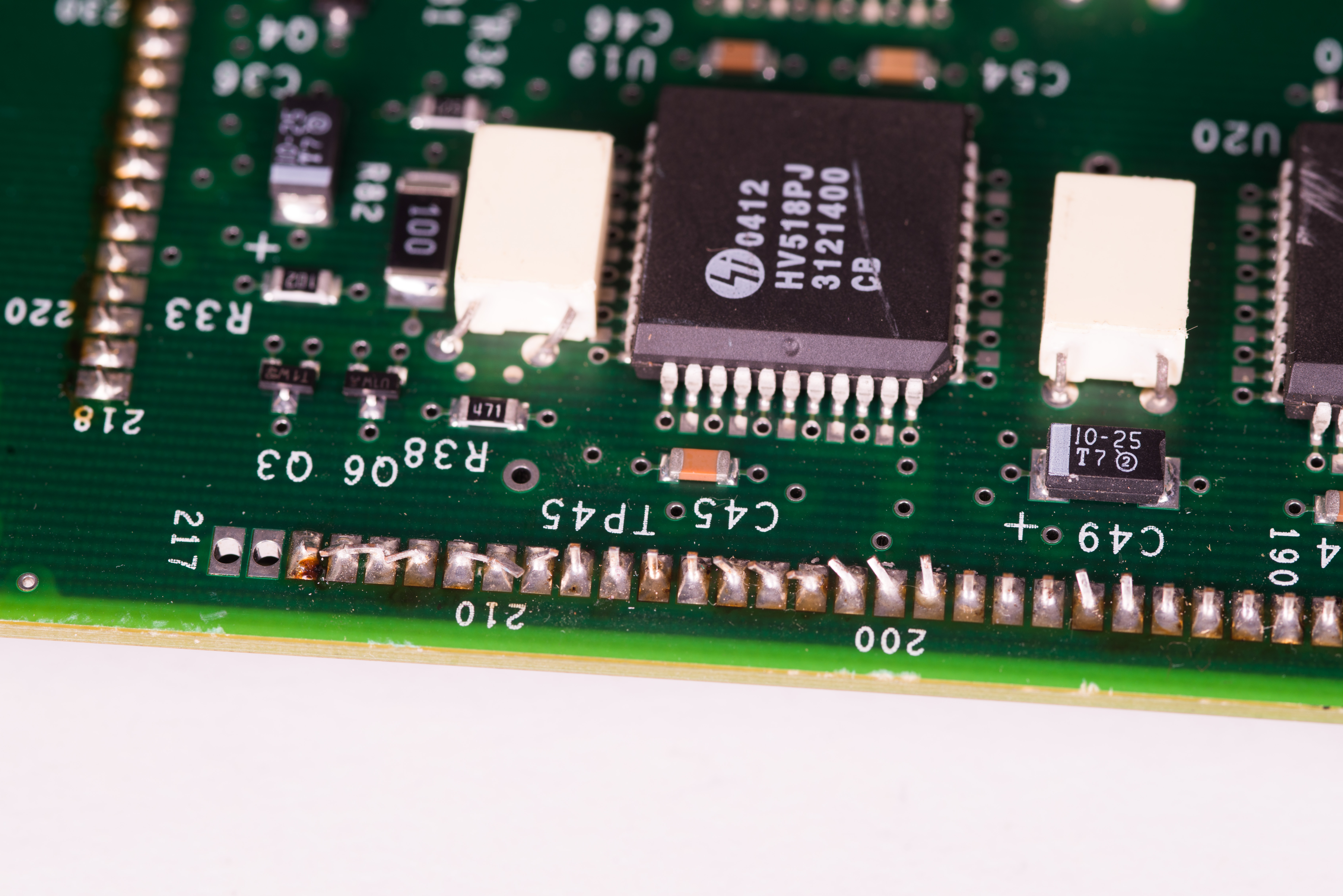
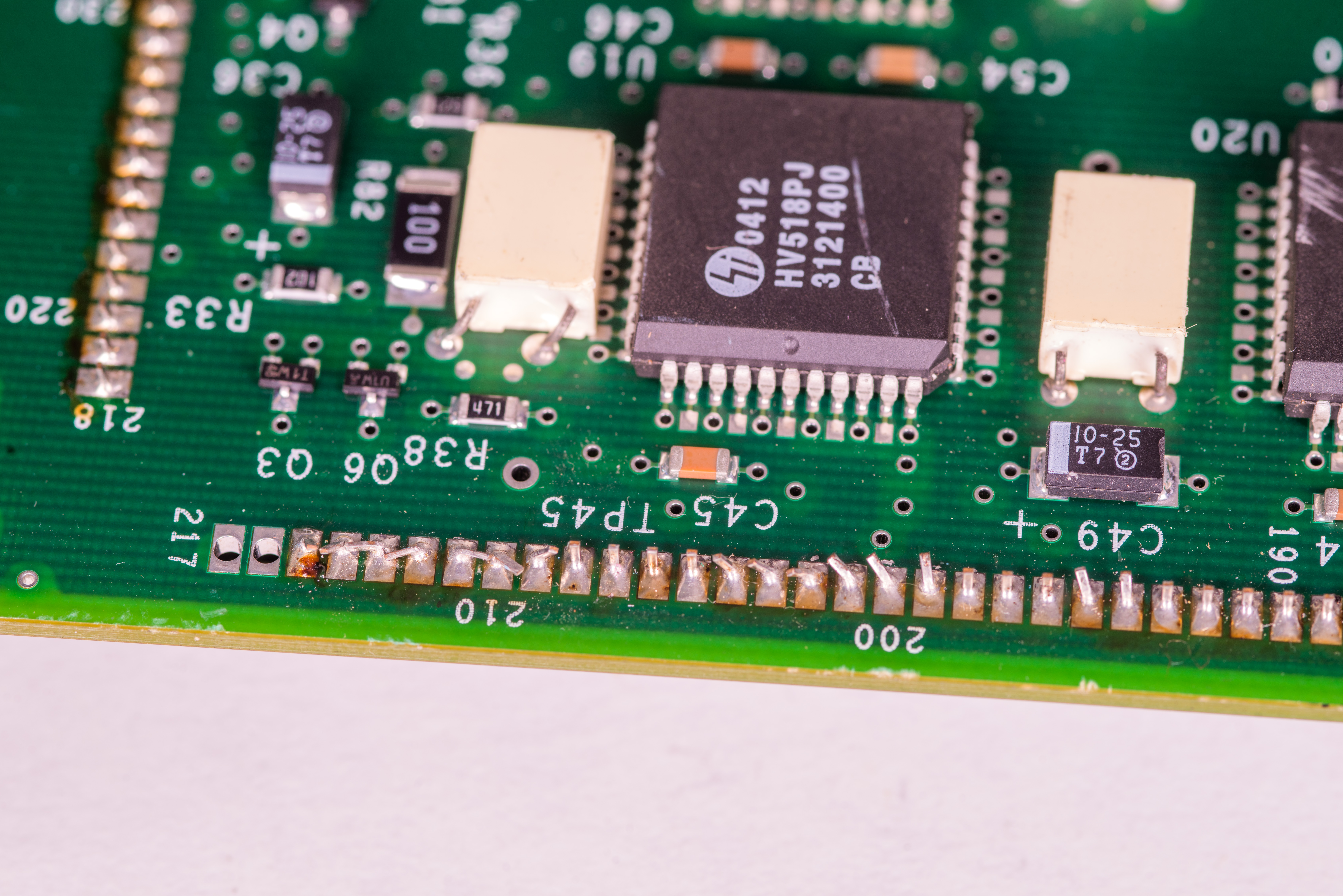
- A11 reference/DAC board
- A11 reference/DAC board, second board
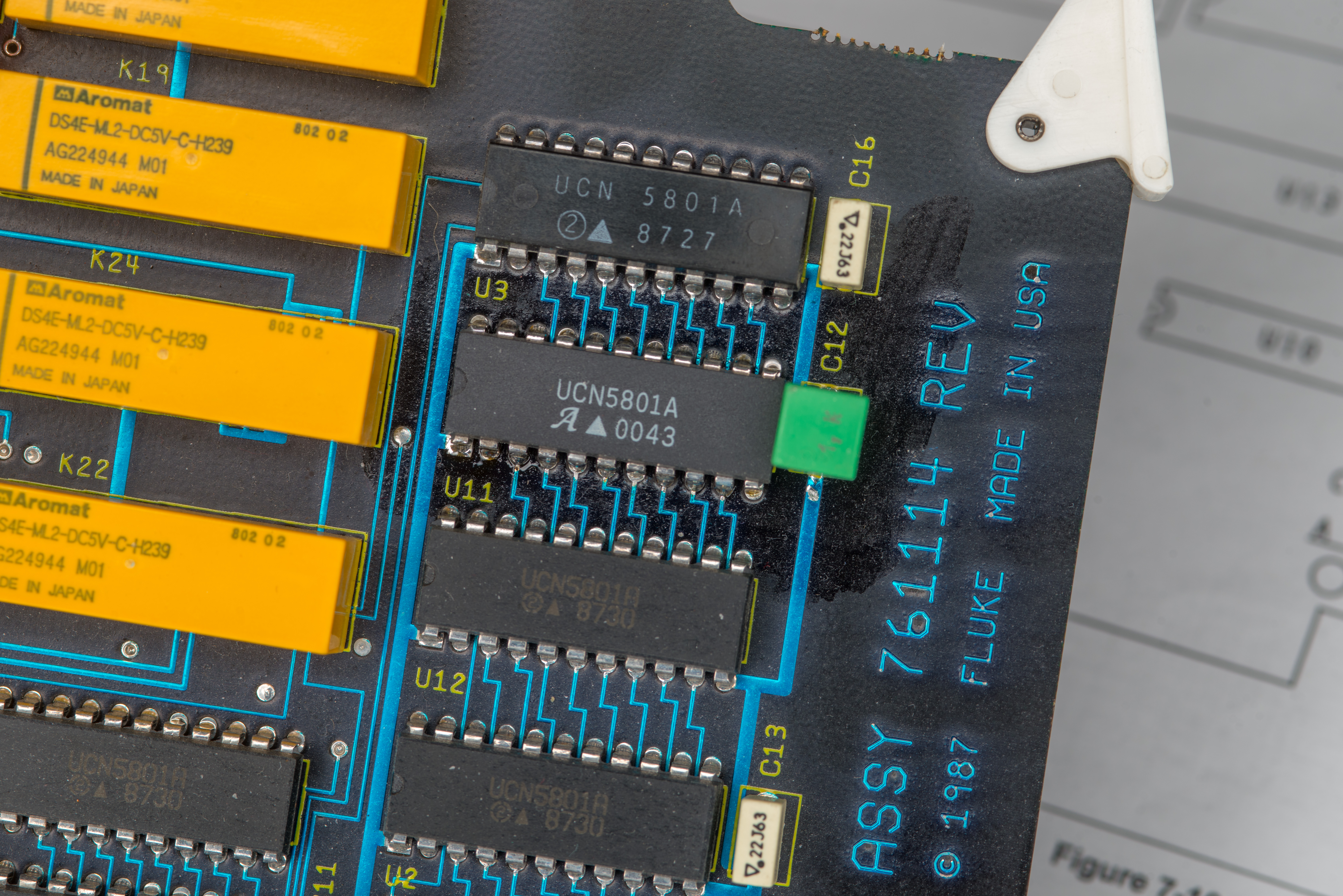
- A8 switch matrix relay board
- A7 current source/high resolution oscillator assembly
- A9 OHM calibration PCBA
- A10 OHM main output PCBA
- Full self-test diagnostics and adjustment procedure
- Initial output adjustment and verification
- Calibration of resistance function
- Temperature stability of resistance function
- Noise performance of the Hulk3 calibrator
- Summary on spent resources
![]()
![]()
![]()
![]()
![]()
![]()
![]()
![]()
![]()
![]()
![]()
![]()
![]()
![]()
![]()
This is our “experimental” calibrator rebuild project, using leftovers and spare donor boards from previous Fluke 5720A rebuild projects. Most of the boards have major failures/missing parts, so this will be the most interesting educational project, showcasing troubleshooting and design of high performance analog instrument done by Fluke grey beard in late 1980’s.
Remember, buying broken or even listed “tested good” used 5700A below market price and fixing it likely will end up as bad expensive exercise, when all hidden costs are considered and accounted for. Paid cost for such a unit WITH the proper repair, long-term stability verification and demanding calibration adjustments will easily exceed cost of buying a fully tested and calibrated unit from reputable source/distributor. So even if you buy complete calibrator for “low price” $5K, you can be easily be rewarded with just pile of unstable/non-fixable parts that would need another $XXK to get even just working again, leave alone meeting specifications.
So how would a dedicated person make the dream to have high-performance calibrator at home to come true, without donating both arms, legs and eyes to nearest Fluke Calibration branch? No escaping the dream today – go build our own calibrator from scrap parts! It is possible but not easy.
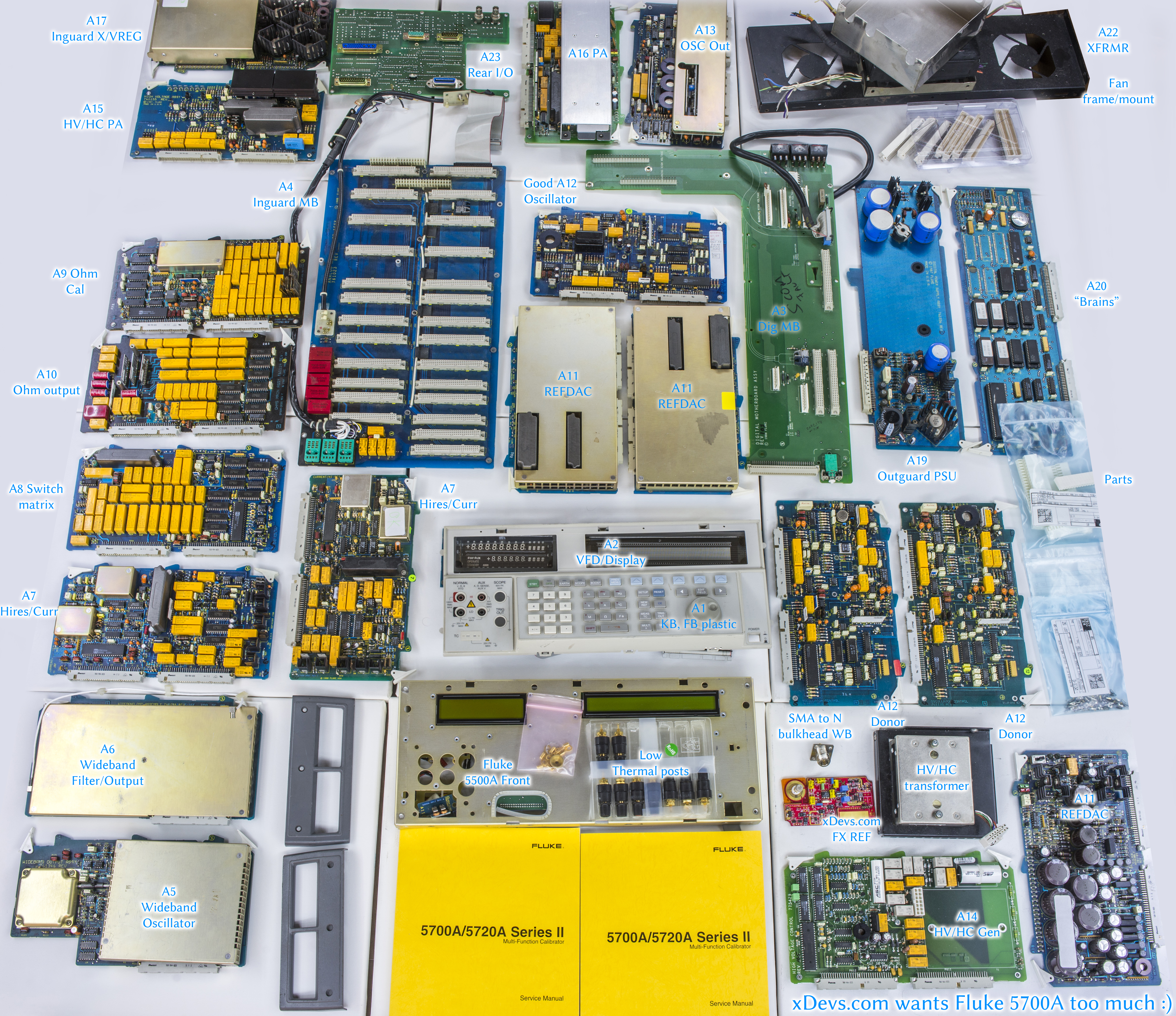
Image 1: Random bits and pieces, lego-version of the 57xx series calibrator hardware
Disclaimer
Redistribution and use of this article, any parts of it or any images or files referenced in it, in source and binary forms, with or without modification, are permitted provided that the following conditions are met:
- Redistributions of article must retain the above copyright notice, this list of conditions, link to this page (https://xdevs.com/fix/hulk3/) and the following disclaimer.
- Redistributions of files in binary form must reproduce the above copyright notice, this list of conditions, link to this page (https://xdevs.com/fix/hulk3/), and the following disclaimer in the documentation and/or other materials provided with the distribution, for example Readme file.
All information posted here is hosted just for education purposes and provided AS IS. In no event shall the author, xDevs.com site, or any other 3rd party, including Fluke be liable for any special, direct, indirect, or consequential damages or any damages whatsoever resulting from loss of use, data or profits, whether in an action of contract, negligence or other tortuous action, arising out of or in connection with the use or performance of information published here.
If you willing to contribute or add your experience regarding instrument repairs or provide extra information, you can do so following these simple instructions
Manuals and documentation
Fluke does provide all main manuals, including service information for these older calibrators, right on the product page, without requirement of any registration or access requests, unlike Tektronix or Keysight web-sites. Thumbs up for Fluke, way to host the data on your product page, not hiding behind registration forms, “ask a consultant” or other big-dollar marketing obscurity.
Brochure: The 5700A/5720A MFC: Taking Accuracy to New Level
Fluke 5700A/5720A Series II Operator Guide, May 1996, Rev.1
Fluke 5700A/5720A Series II Operators Manual, May 1996, Rev.2
Fluke 5700A/5720A Series II Operators Manual Supplement, Feb 2008, Issue 5
Fluke 5700A/5720A Series II Operators Manual Supplement, Feb 2008, Issue 9
Fluke 5700A/5720A Series II Service Manual, Nov 2007 w/o schematics
Fluke 5700A/5720A Series II Service Manual Supplement, Issue 6
Fluke 5700A/5720A Series II Service Manual Supplement, Issue 9
Fluke 5700A/5720A Series II Getting started, March 2002, Rev.2
Fluke 5700A/5720A Series II Getting started Supplement, Issue 6
Fluke 5700A/5720A Series II Remote Programming Reference Guide
Fluke 5700A Instrument Security Procedures
Fluke 5720A Instrument Security Procedures
Tech data: 5700A->5720A Upgrade Service
Model 5440A-7002 Low Thermal Test Lead Set – Specification
Fluke 5700A, 5720A CE Declaration of Conformity
Service notes
First goes the most important document for repairs/maintenance – 570-page service manual. Credits for hosting it first going to KO4BB portal. We are lucky to also have schematics, list of parts, assembly drawings of the boards included in it!
Fluke 5700A MFC Service Manual with schematics, Rev.9,3/96, March 1996
Fluke 5700A Series II/5720A MFC Service Manual with schematics, Rev.1,3/02, June 1996
5700A Series I and 5700A/5720A Series II difference
According to An evaluation of the 5700A Series II Artifact Calibration document, major changes in Fluke 5700A/5720A Series II are related to Artifact Calibration and high-frequency AC voltage. Artifact Calibration was improved on a number of ranges, to minimize biases. A new interpolation algorithm is also used for lower ACI ranges to provide better performance.
From hardware standpoint, Model 5720/5700 Series II calibrator has a modification to the in-guard microprocessor circuitry and firmware to minimize noise in the low millivolt ranges. Also, because of the tighter specifications of the 5720A there are more carefully selected components than in the standard 5700A. Lot of circuit tweaks and changes are on A11 REFDAC and A16 Power Amplifier inguard assembly modules. Many tweaks and minor changes on every board in 5720A level hardware address better reliability and stability of the calibrator. Digital processor board A20 firmware are also updated as a result to reflect added functionality.
Project concept and workflow
Over the course of the project author and other members of xDevs community have learned a great lot about inner workings and troubleshooting non-obvious soft-failure issues, such as out of specification output drift or excessive noise. These problems are not detectable by instruments self-diagnostics procedures and can be hard to catch. We hope to provide great amount of details in this article about 5700A or 5720A, however some of this knowledge is restricted to internal use and will not be published. If you have specific question about 5700A/5720A/5730A you can try asking us online on this page or via email.
Overall approach is to start rebuild of the 5700A “Hulk-3” from the basics – such as establishing metalwork chassis and start populating it with electronic modules. First to test and debug would be power supply modules, main processor, front panel display/keyboard. These modules hardware and firmware operation is main milestone before any analog functionality can be enabled and troubleshooted.
Modularity and 5700A/5720A flexible diagnostics
Fluke designers kept everything very modular making it easier to troubleshoot, service and follow the signals around. Many of the local functions are contained within one PCBA/module, allowing great deal of per-module repair or diagnostics. Self-test procedure is also very elaborate and runs about 20 minutes to perform hundreds of test and point measurements to provide you comprehensive diagnostics. Most of the circuitry is tested and many faults can be detected just from the self-test messages.
This is great help for the Hulk project here, otherwise repairs would be much harder to diagnose and correctly determine faulty conditions in many mixed cases. Having “spare” working 5700A/5720A to make “reference” measurements it can be also very helpful, but I’ve deliberately trying to avoid such appoarch to minimize risk of accidental damage to good instrument.
Wise approach here is to test minimum amount of modules/boards first , to ensure voltage regulation/power supplies correct operation and all digital control/interfacing work. Experimentally we determined various valid hardware configurations for functionality checks, as outlined in table 1.
| Config, Hardware setup | Modules installed/used | Provided functions |
|---|---|---|
| A, Inguard digital + power test | A3+A4 + A19+A20 + A1+A2 Front panel + A21 | Unit boots firmware, display VFD, hang on error “Guard crossing” |
| B, Inguard + outguard power test | Same as A + A18 PCBA | Unit hangs on “Guard crossing”, but now can check outguard power pre-regulator / filter |
| C, Outguard power test, cross-guard interface | Same as B + A17 PCBA | Unit boots, allow to navigate menus, but no any outputs/functions |
| D, DCV function test | Same as C + A8 and A11 PCBA | Unit boots, allow to output 220mV,2.2V,11/22V DC Voltage, ACAL can be run |
| E, DCV+Resistance function test | Save as D + A7,A9,A10 PCBA | Unit boots, adds Resistance and DC Current 220 µA – 220 mA, ACAL can be run |
| F, ACV function test | Same as E + A12,A13 PCBA | Unit boots, adds ACV and ACI functions, sans 2.2A and 220V,1kV ranges, ACAL can be run |
| G, HV/HC test | Same as F + A14,A15,A16 PCBA | Base configuration, adds 2.2A and 220V,1kV ranges. ACAL fully enabled |
| K, Wideband option | G + Add optional A5+A6 PCBA | Full configuration with 2.2mV – 3.5V 30MHz Wideband option |
| W, Boosted option | Connect 5725A to expansion port | Enables 11A DCI and ACI, extends V/F limits for 1kVAC range |
| X, Boosted option | Connect 5220A and 5205A to expansion ports | Enables 20A DCI and ACI, extends V/F limits for 1.1kVAC 100kHz with 200mA drive |
Table 1. Hardware modules configuration supported by the 57xx series calibrators
Configurations in bold letters allow to complete self-test and artifact calibration procedures to be completed without errors. Calibrator in this article will be rebuilt to F level. We have no plans to go further, as that would require finding rather expensive A14/A15 and WB modules. Since xDevs.com already have all these in main Fluke 5720A “Hulk-1” and “Hulk-2” calibrators, it was decided not to duplicate the functionality here.
This grading is totally made up and not used anywhere in Fluke documentation, but I figured it would be handy for further discussion in repairs to know exactly what boards are populated in the calibrator.
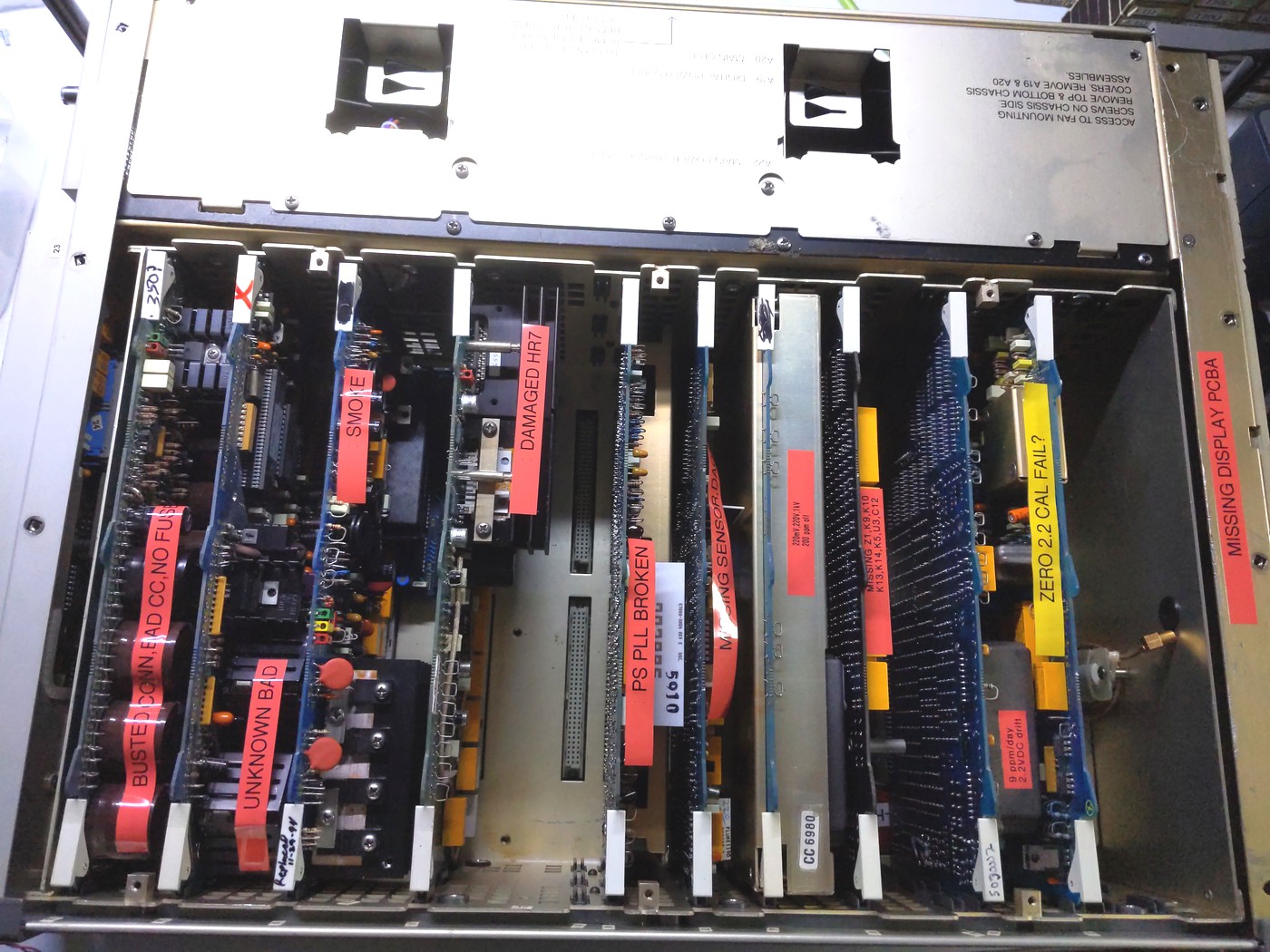
Fluke 5720 “C” Hulk-III build
Let’s go ahead with worklog on repairs and testing, module by module, part by part, as we find the problematic circuits.
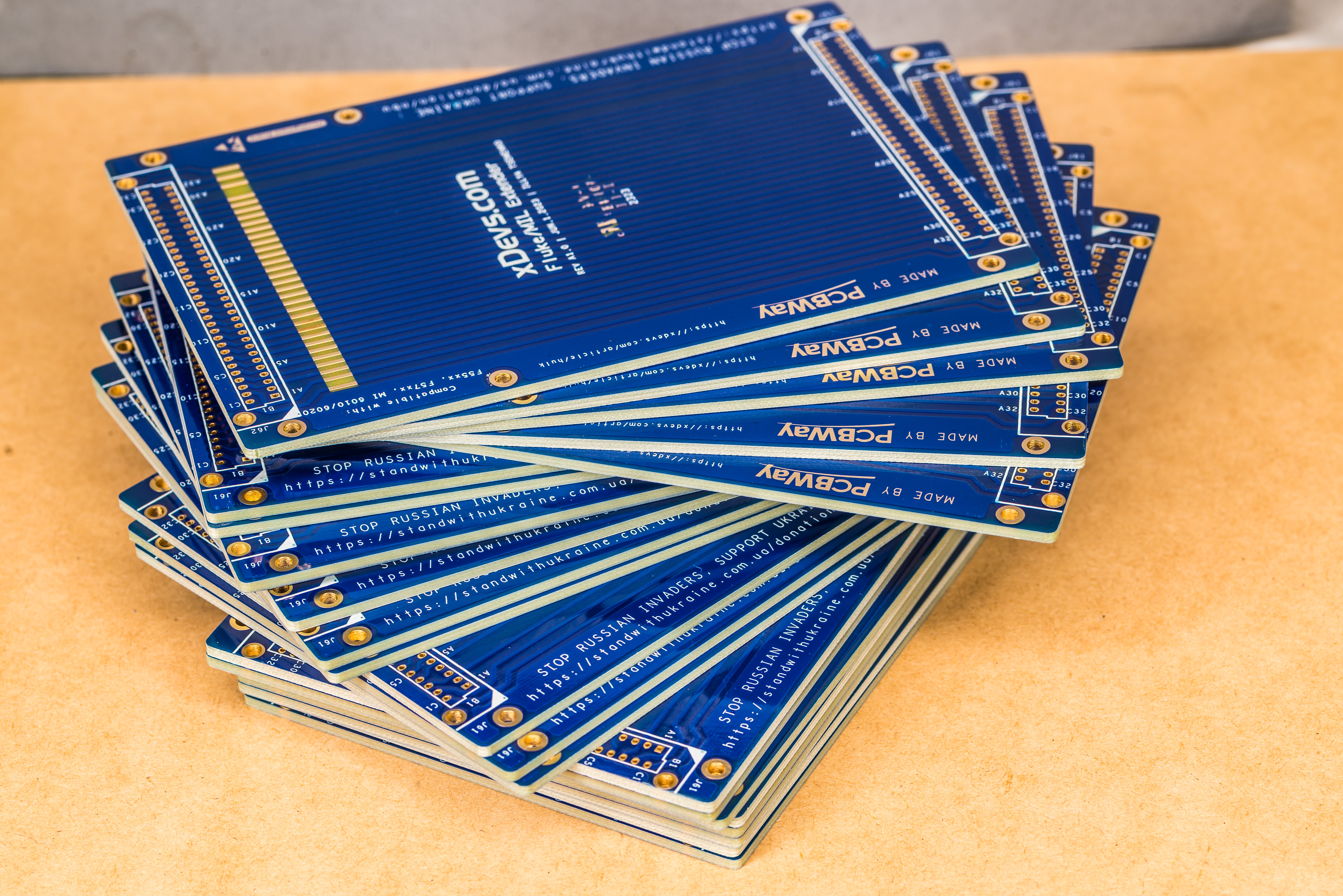
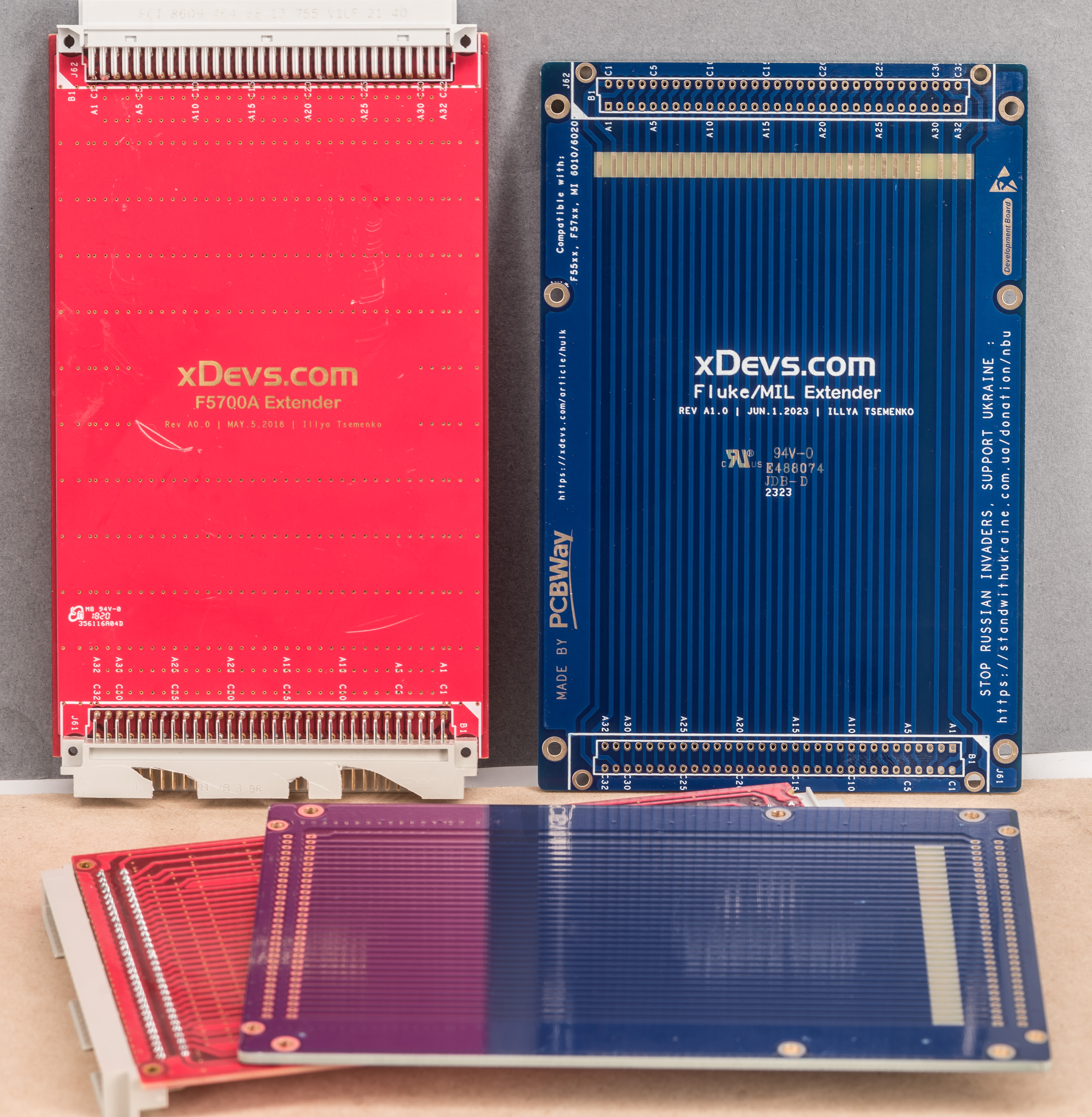
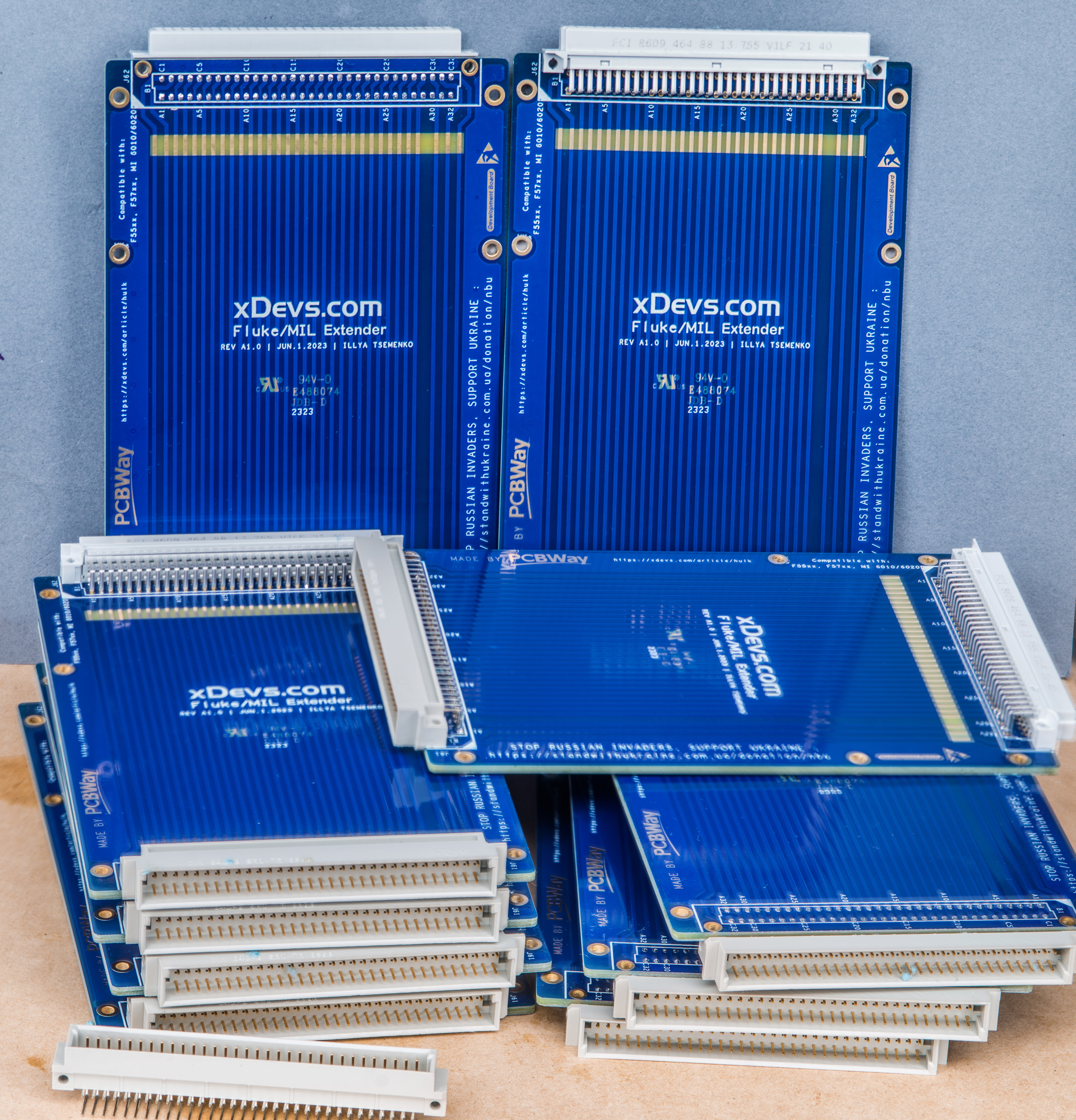
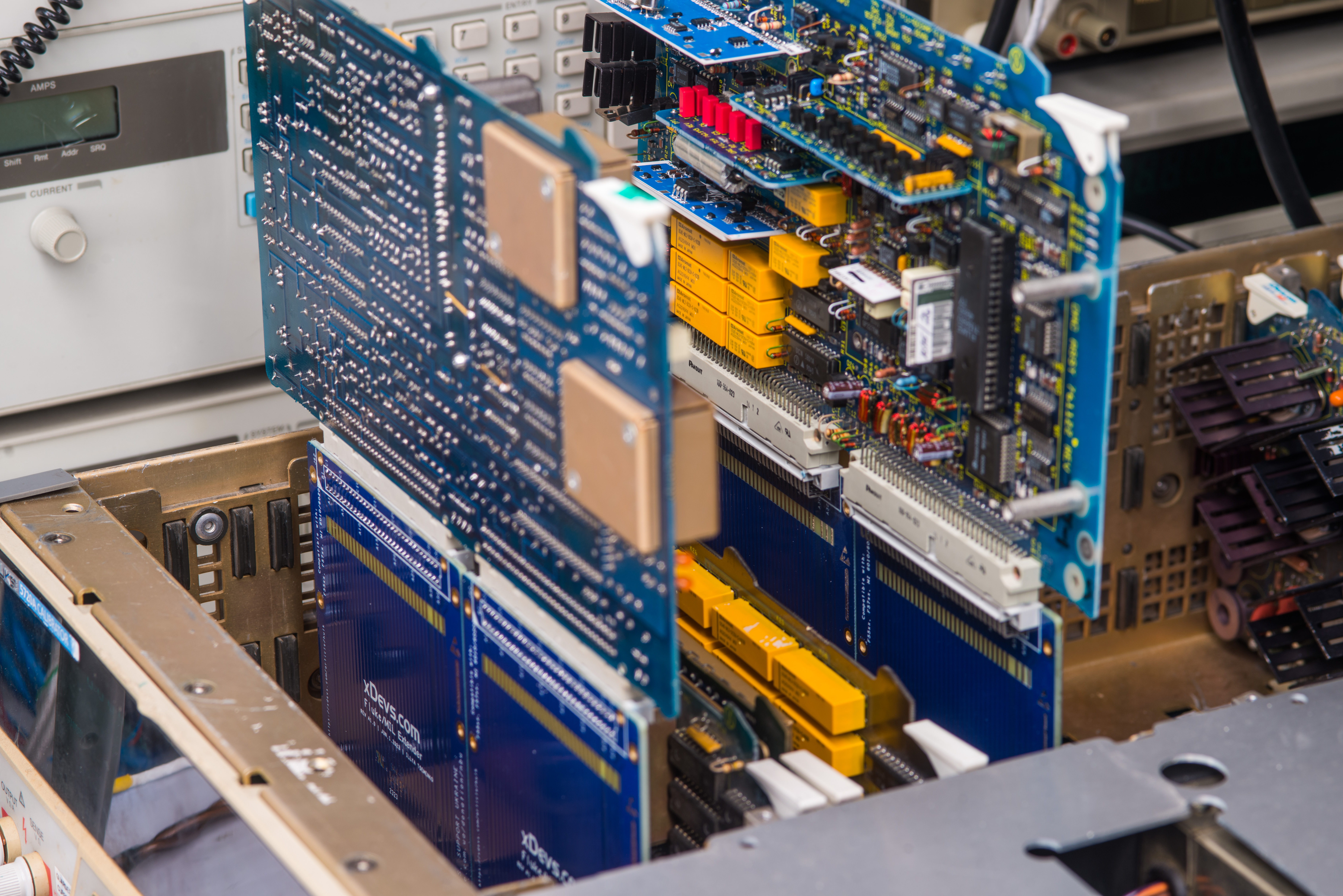
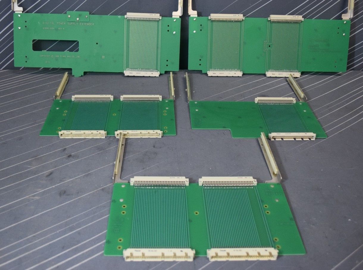
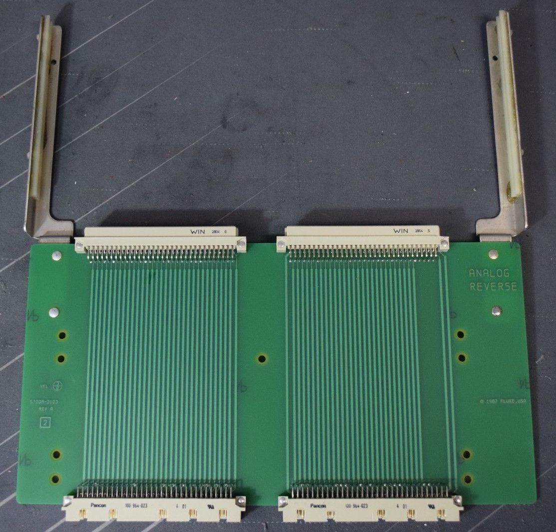
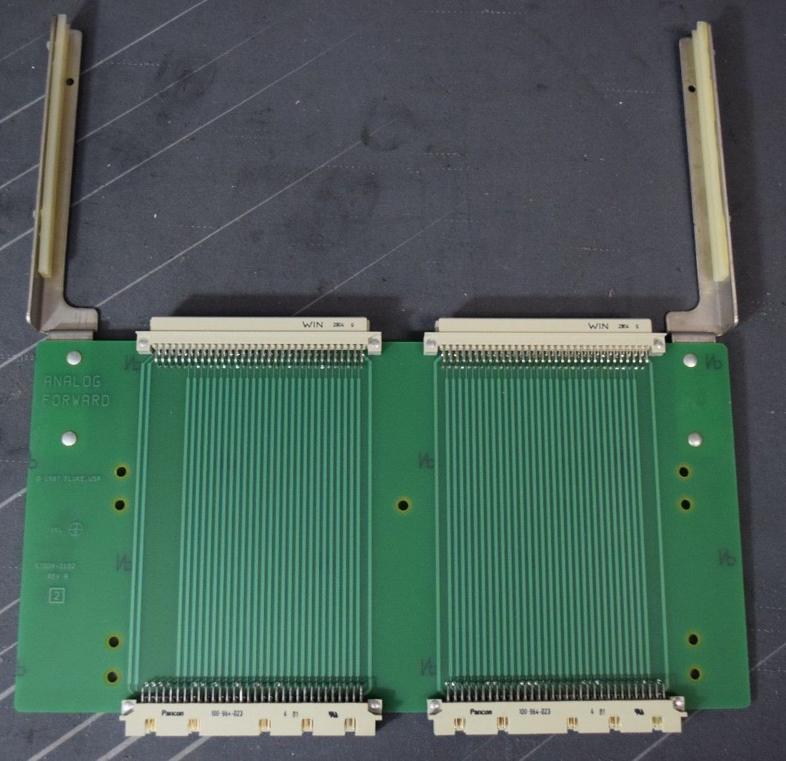
Extender boards 2023
I have designed and ordered a set of extenders for my first 5720A project back in 2018. However, that design had mechanical and electrical issues, prompting me to make improvements and obtain new extenders today. The board extenders play a crucial role in gaining access to various test points for troubleshooting, particularly for complex equipment like the Fluke 5720A calibrator.
The important enhancements for the new 2023 extender board design are outlined below:
- Matching standard DIN 41462 connector shrouds. Old 2018 extender required trimming 3 mm of PCB from each edge to resolve interference with the connector housing. The new design aligns perfectly with the connector, eliminating the need for Dremel help.
- Reducing the number of layers from four to two and increasing isolation spacing between traces: The original extender had issues with leakage and self-test failures when used with High-Voltage/High-current modules.
- Increasing the thickness of the PCB for a more robust and rigid connection: The new extender boards will have an increased thickness to ensure a stronger and more secure setup with modules.
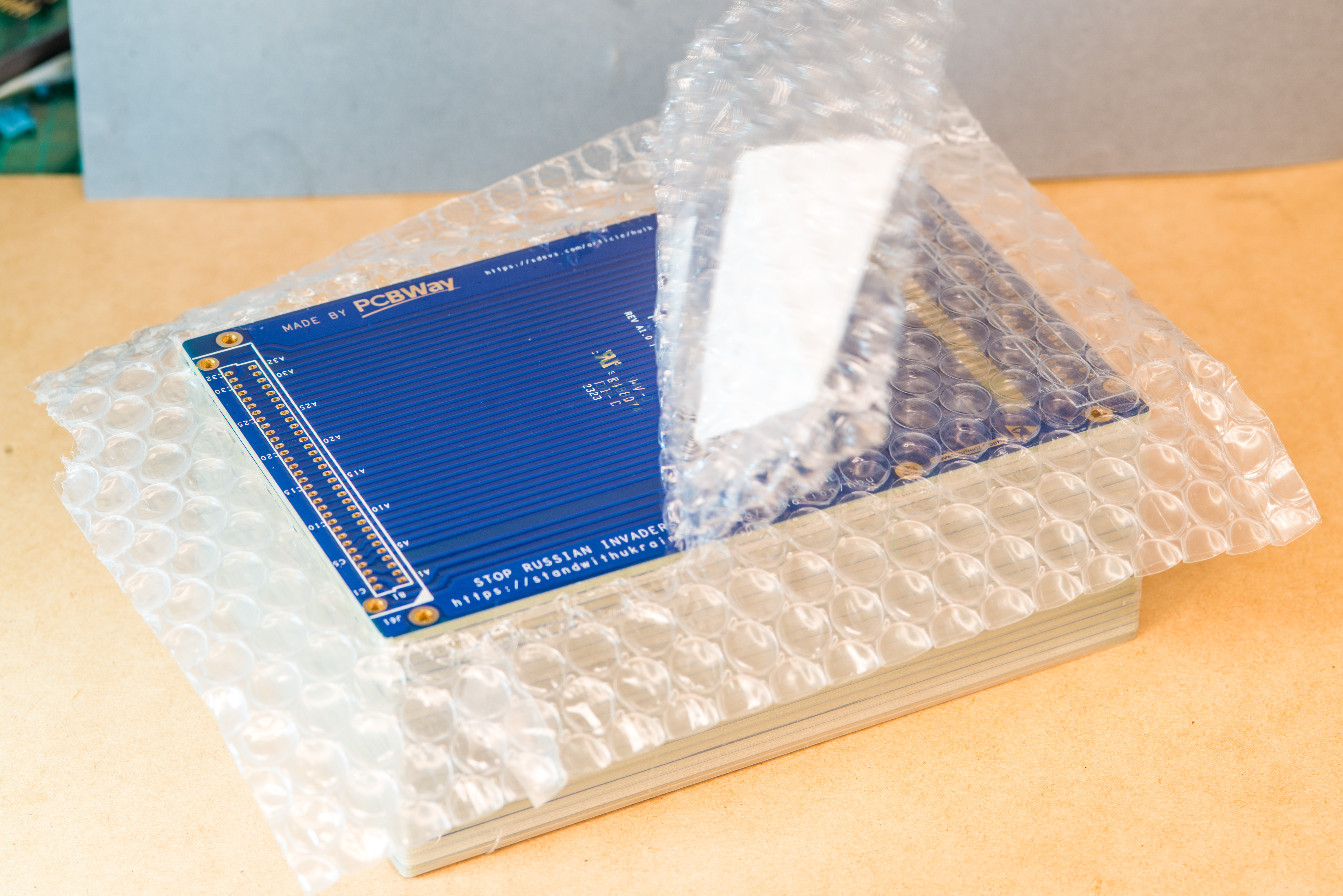
- Add silkscreen and solder mask markings. 2023 design now has helpful markings such as the project URL.
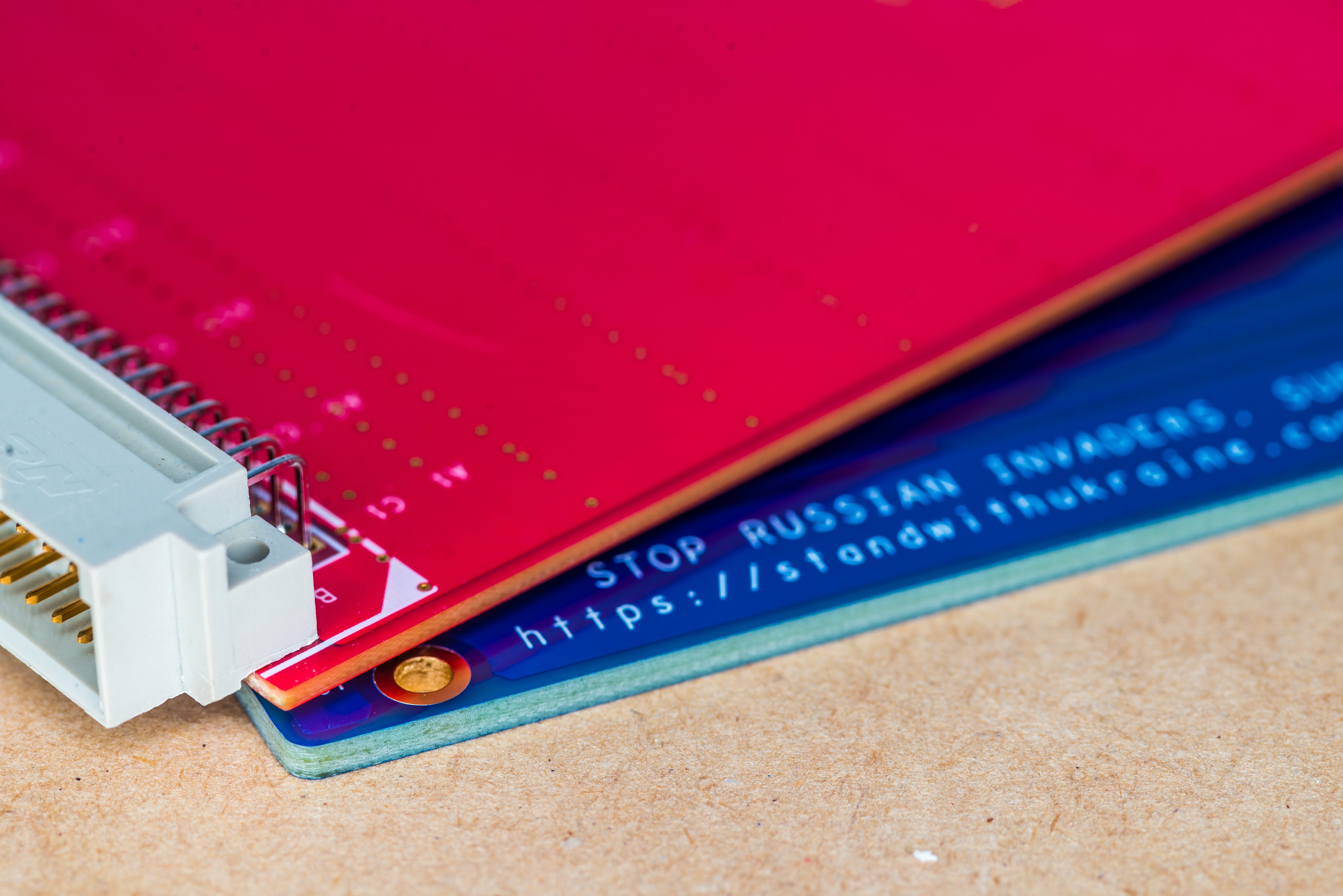
- Increasing awareness of the unprovoked russian invasion and the terror unleashed on Ukraine. It is vital to raise awareness about the ongoing conflict and support those affected.
By implementing these improvements, new 2023 extender boards addressed the previous design’s shortcomings and now provide a more efficient and reliable solution for troubleshooting and calibration tasks in 5720A.
PCBway is the fabricator responsible for producing these new upgraded extender boards.
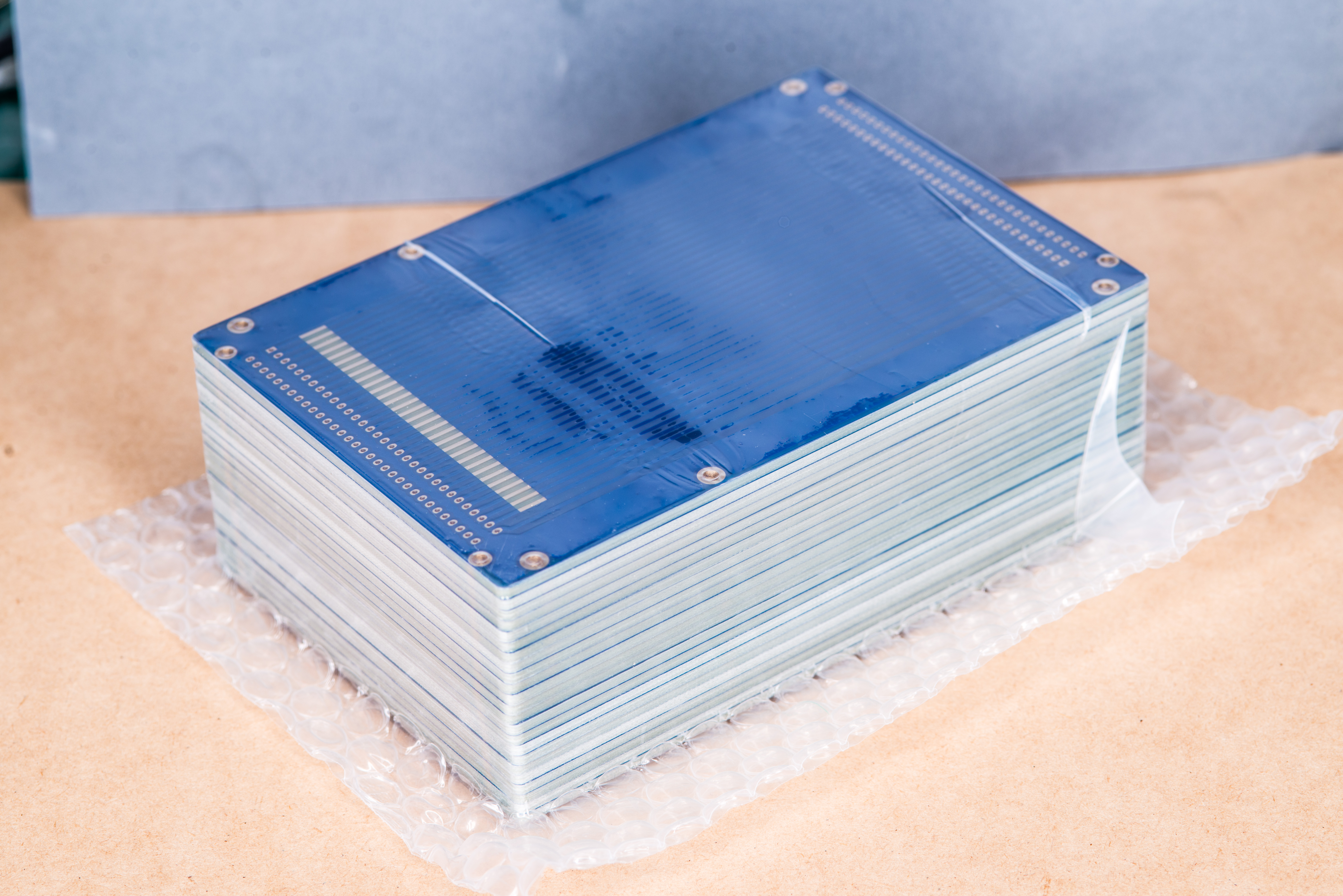
This is a simple 2-layer TG150 FR-4 PCB, with ENIG plating useful for longer shelf life. PCBway made these boards in a few days and promptly shipped using DHL international delivery service. It is common for PCB manufacturers to utilize the available space on a panel effectively, maximizing production efficiency. In some instances, there is extra space on the panel and manufacturers may include a few additional boards as a bonus. In this case, such nice addon of the PCB manufacturer was evident as the order for twenty boards resulted in the receipt of 21 boards. Additional board could serve as a backup or used for testing, prototyping, or future projects. It was a pleasant surprise that not only demonstrated the manufacturer’s commitment but also provided added value to the order :).
PCBway standard PCB service was used this time but with our custom design specific parameters, which are described in table below. To access the Gerber files and view the project page, simply click on the parameter table provided.
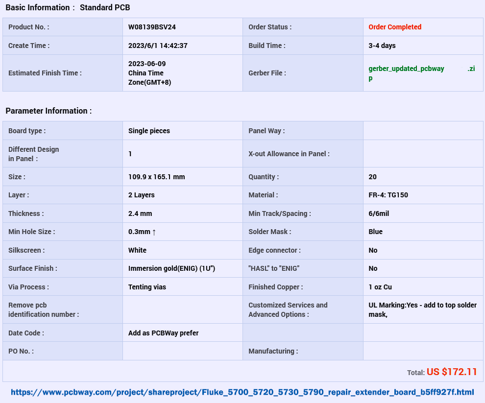
I have goofed up a little by setting UL marking in top solder mask instead of silkscreen, which clearly opened some traces on PCB, but it’s no big deal :)
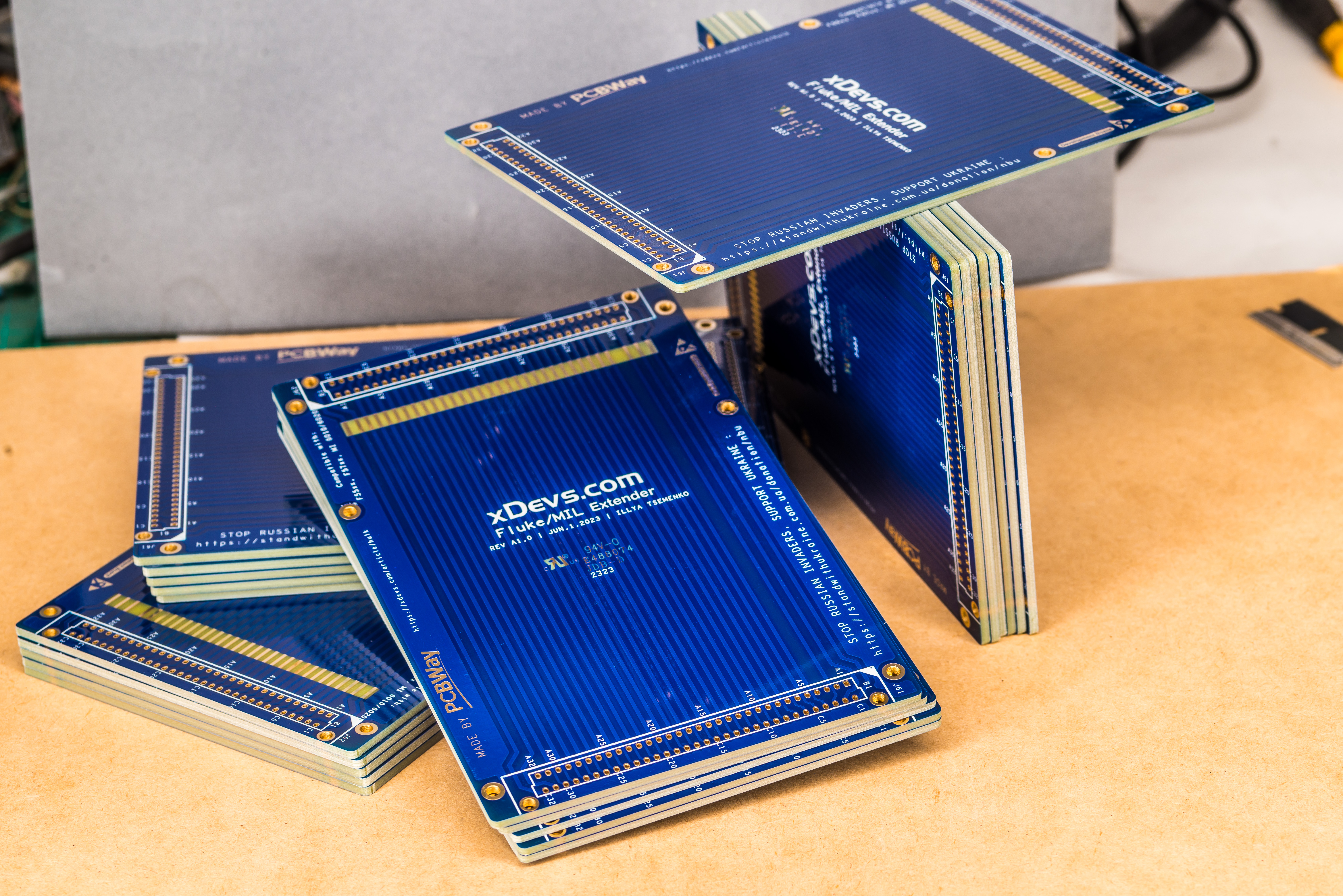
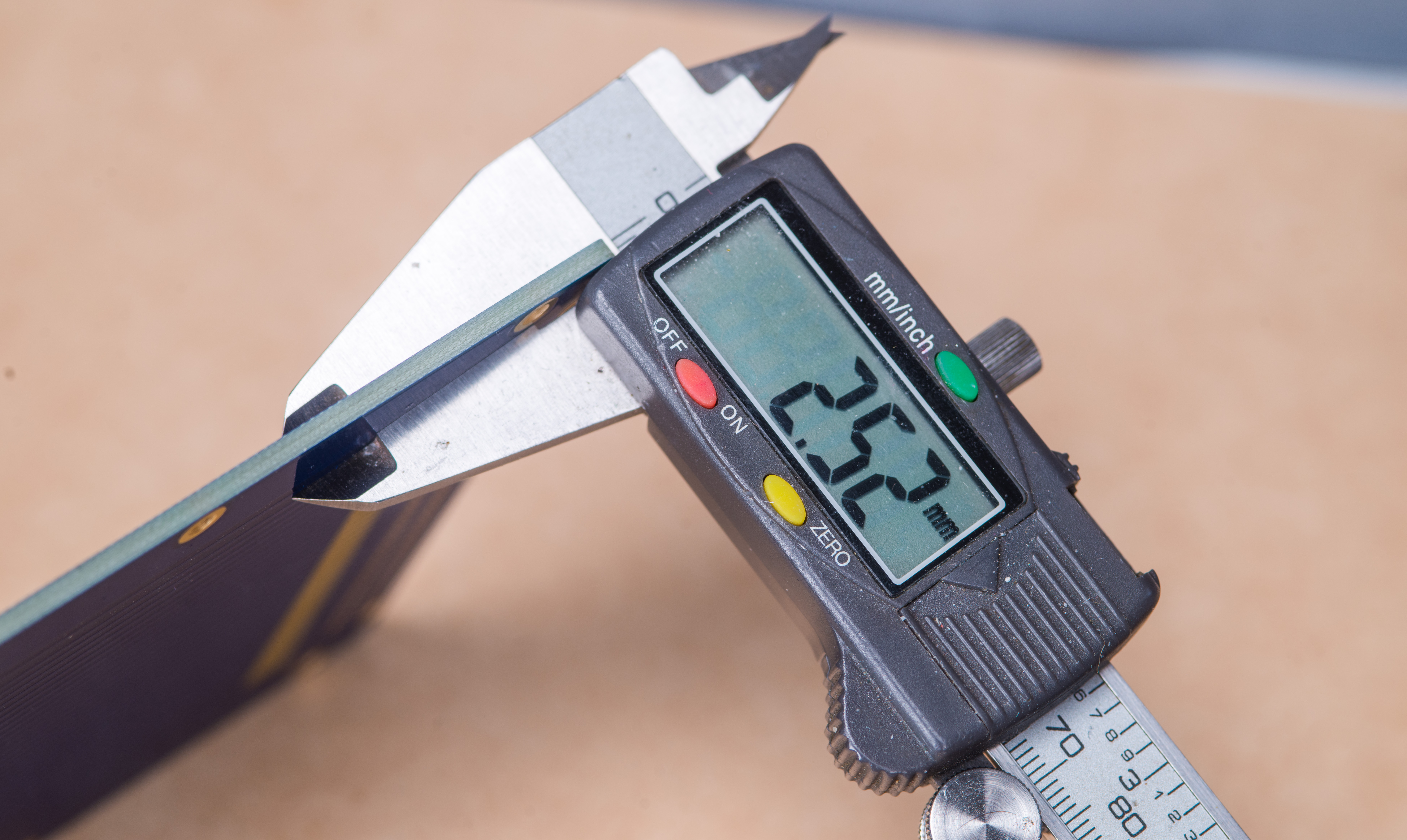
The quality of these improved extender boards is very nice. In particular, the thicker and more rigid 2.4mm substrate of this latest version sets it apart from the one I designed back in 2018. The upgrade in substrate thickness not only adds mechanical rigidity but also provides better isolation from traces on TOP and BOTTOM layers, which is important for use in Fluke 5700/5720 calibrator as some traces can carry up to 1000V DC or AC voltage. The sturdiness also provides extra support to plugged in Fluke module during probing.
When testing calibrator’s modules, there is flexibility in deciding what side to place connectors on extender for. If the desired orientation of the module requires easy access to the connectors from the front side, then the connectors will be populated on the top side of the board (with xDevs logo print). On the other hand, some modules in 5700/5720A are installed flipped (back of the module towards calibrator front). For such modules it can be useful to populate connector on reverse side of the extender board.
The decision on the connector placement is based on factors such as the physical arrangement of the modules under test within the system, the ease of connecting external probes, wires or components, and the overall position of the calibrator’s module. By allowing the connectors population from either the top or bottom side, the extender board design can be tailored to accommodate different orientation requirements, ensuring optimal convenience in connecting the module to external devices.
The 5720A’s motherboard connectors have a keying tab to prevent the installation of the module into the wrong port. As a result, if you want to populate the extender in a specific slot, you will need to make cuts in the desired locations of the standard DIN41462 connector housing. This modification allows for proper alignment and ensures that the extender can insert into the desired slot bypassing this limitation.

Fluke also has an original repair kit dedicated to service of 5700A and 5720A calibrators which include five extender cards. I never had this kit in real life, just got photos years ago. These extenders are fancier and much more expensive.
Fluke implemented metal arms with plastic slide guides to facilitate the proper connection of the module under test. These guide bars assist in guiding the module into the connectors with precision.
However, even without these guide bars, the modules fit securely in the connectors due to the reliable grip provided by the 128 pins that firmly hold the connectors and boards in place.
In addition, Fluke has also developed dedicated extenders specifically designed for either front or reverse card orientation.
Extra-long extenders are also used for A19 outguard power supply card and A20 processor card. But I found that usual narrow extenders for inguard work in those positions as well with little bit of care and added support for the length of those A19/A20 modules.
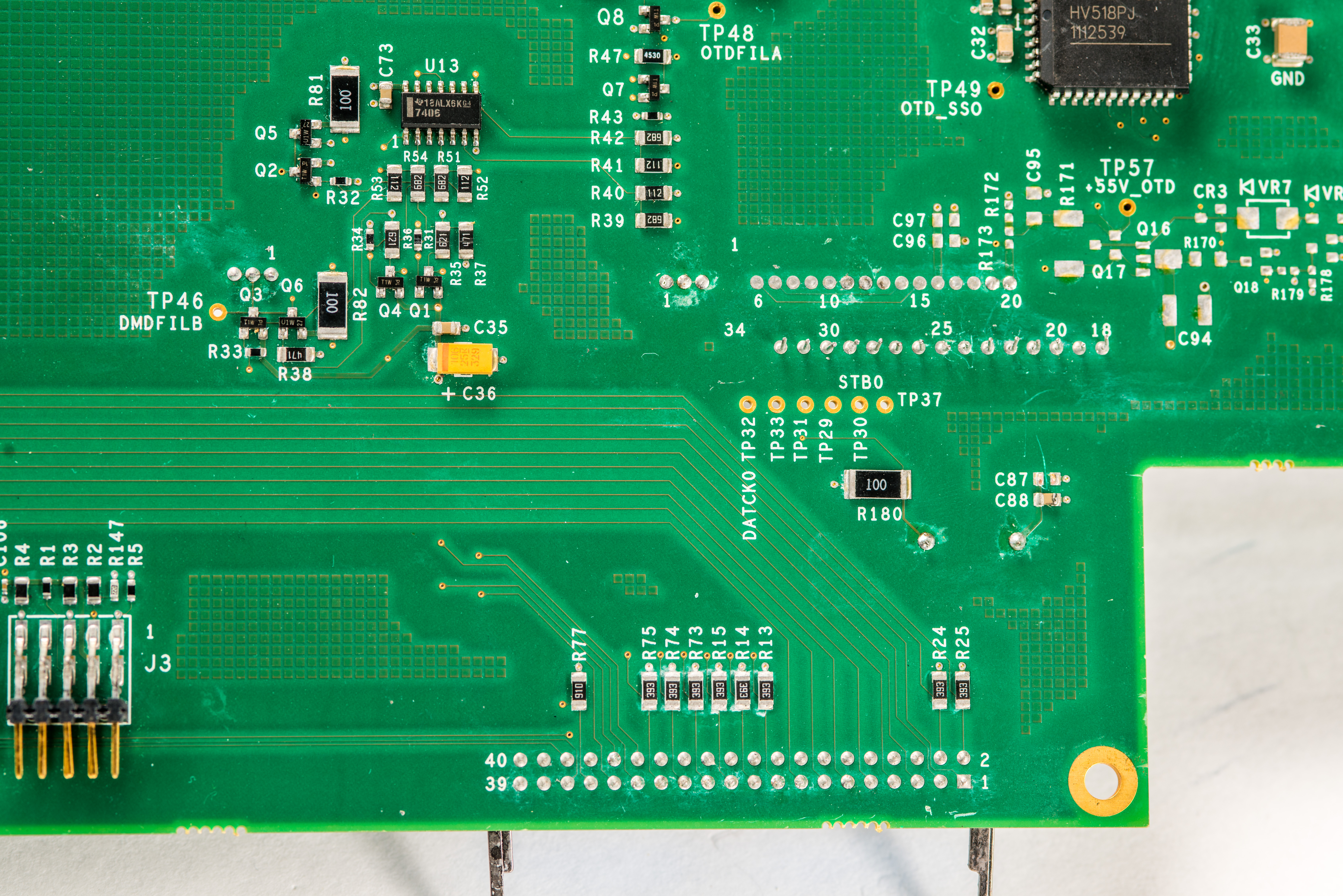
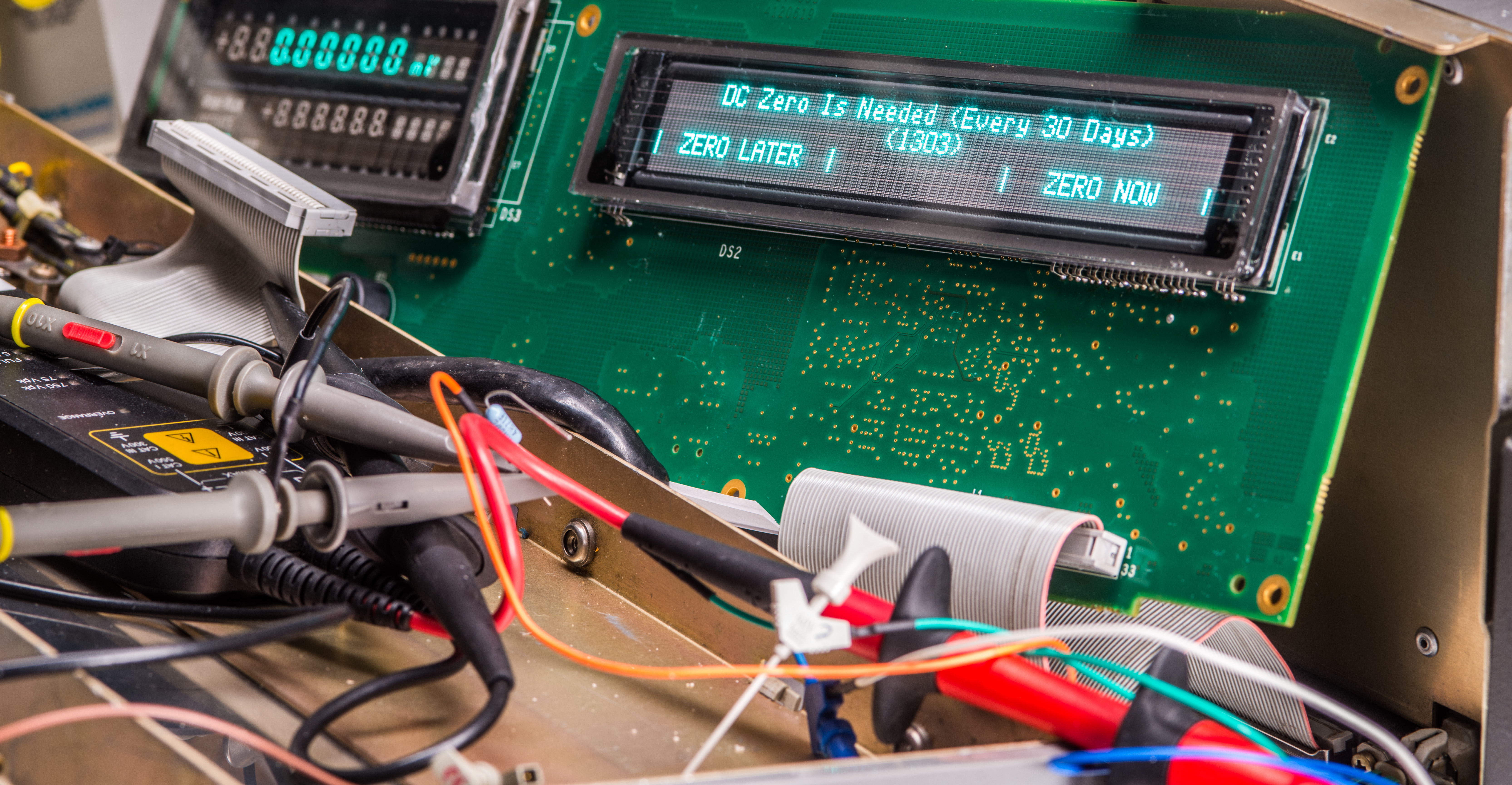
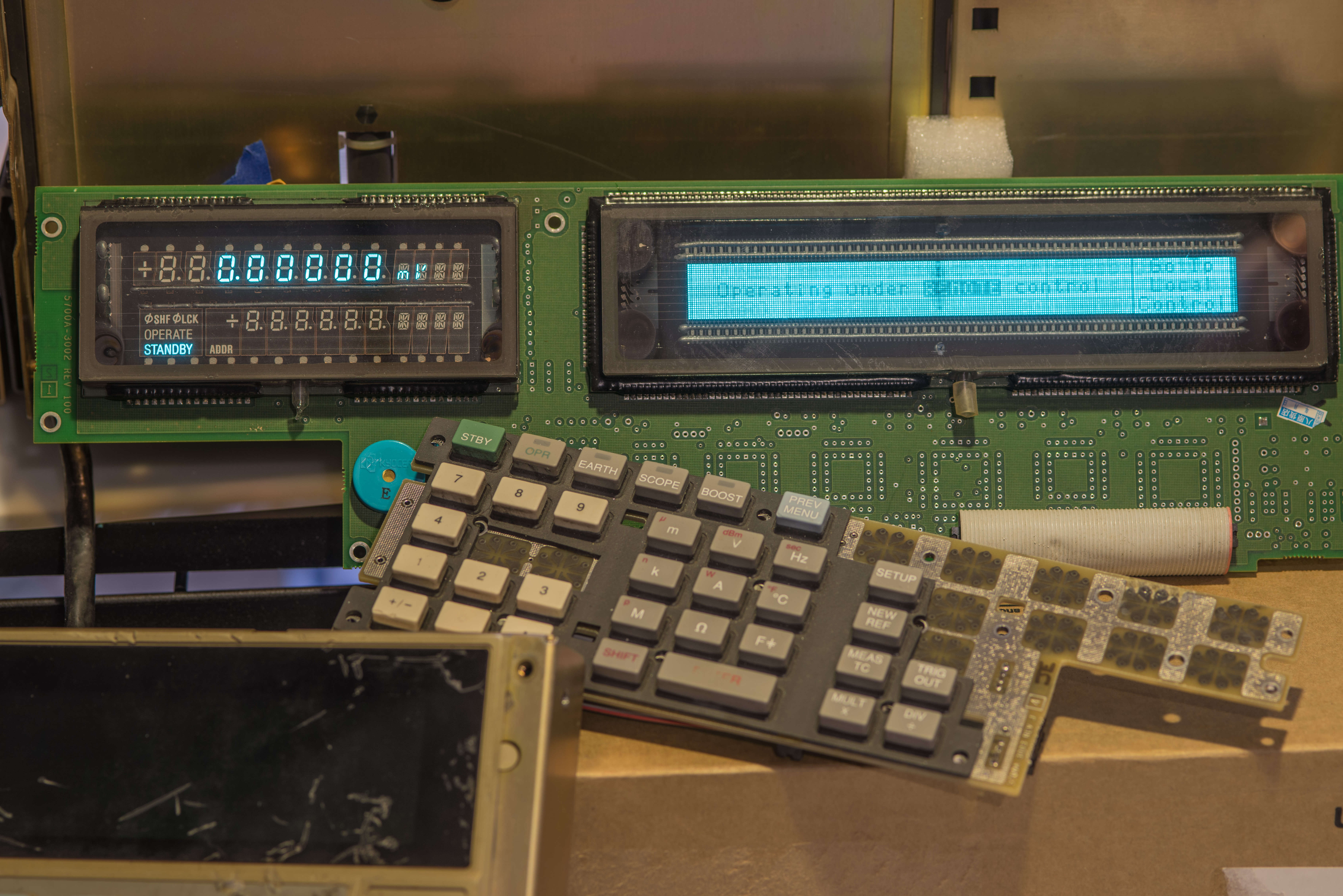
A2 Display front panel PCBA
This board was purchased broken. It is still useful, as calibrator must have controller response from FP to complete boot sequence and operate. Without A2 board calibrator will never finish booting and will not respond to any commands over GPIB or RS232 bus either.
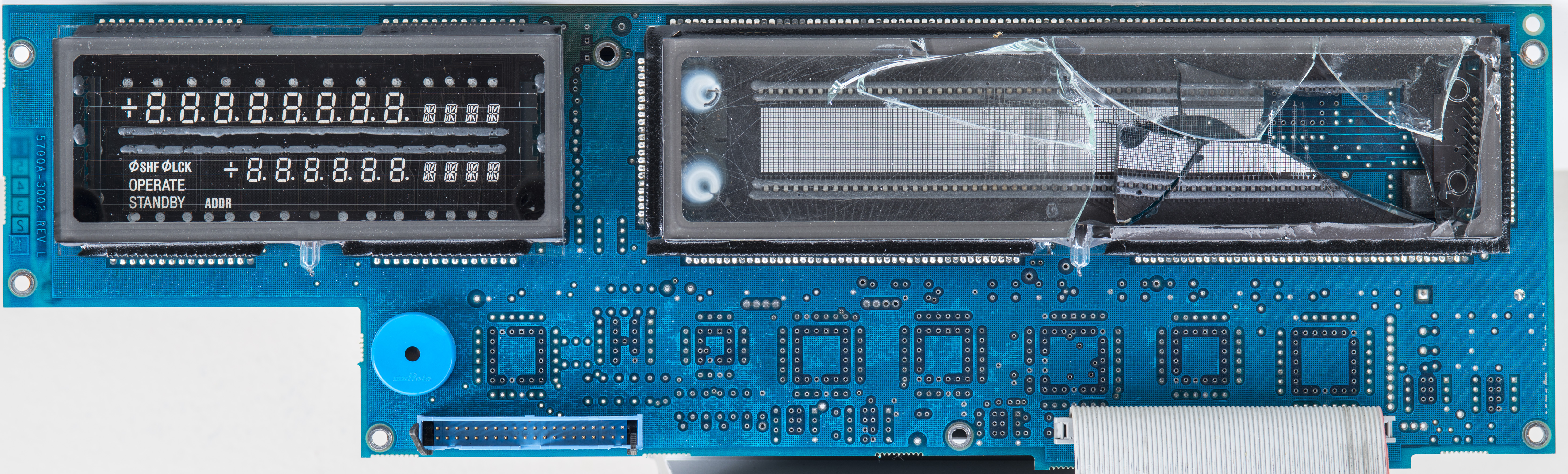
Other than shattered custom VFD glass there seem to be no other damages. Good for us, left VFD designated to display current calibrator status and output signal amplitude/frequency is perfectly fine.
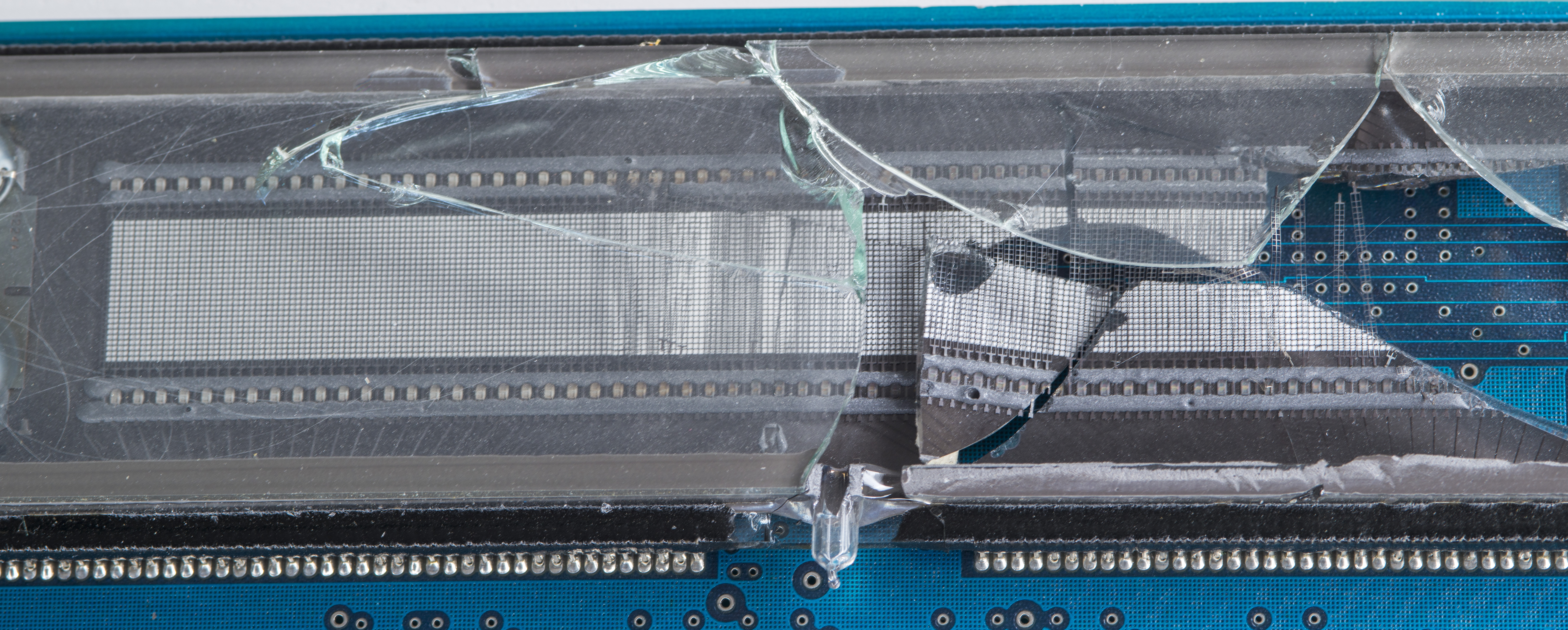
For now we can remove shards and pieces of glass to operate board as is.
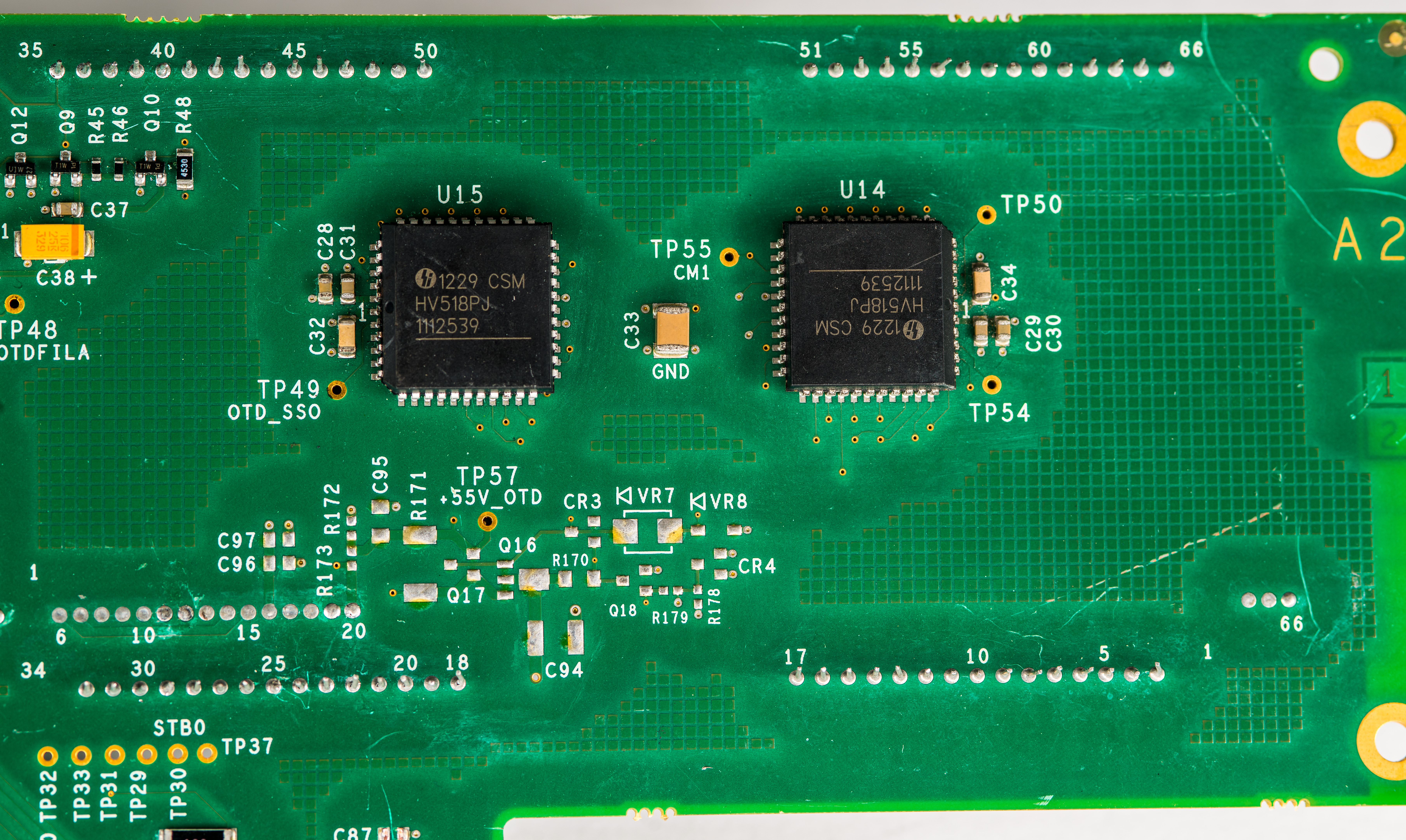
Original dot matrix right VFD was manufactured by Noritake Itron, Model DM256×32. Sadly, this is custom design and not available for replacement that easy.
Maybe in future we can buy another A2 donor board but with shattered left display? :)
A2 2012 version display front panel PCBA
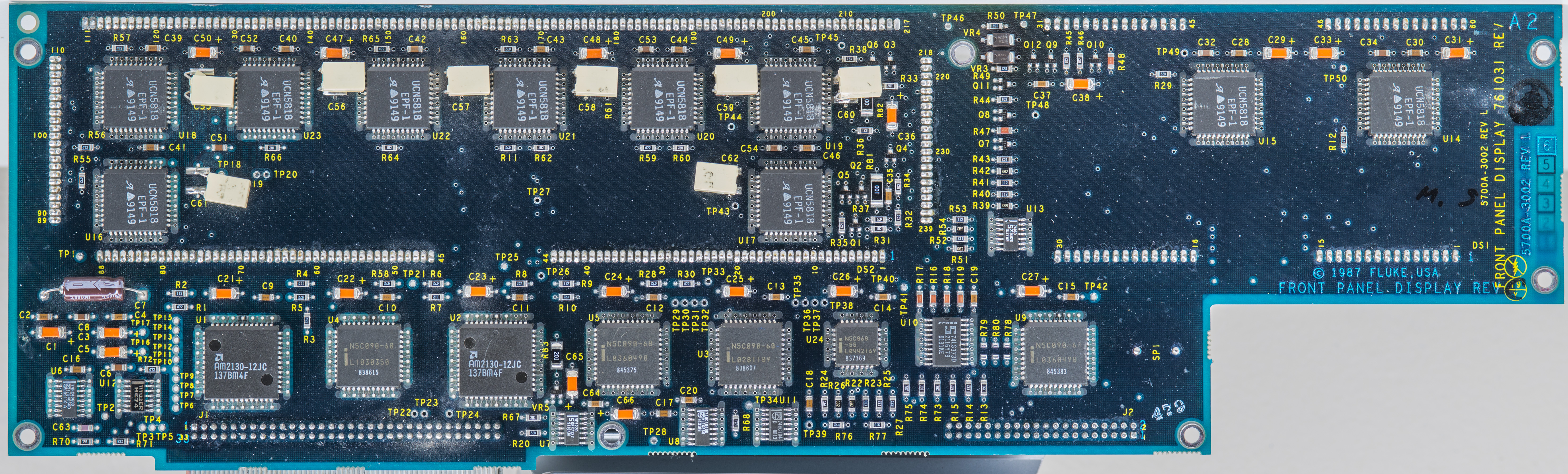
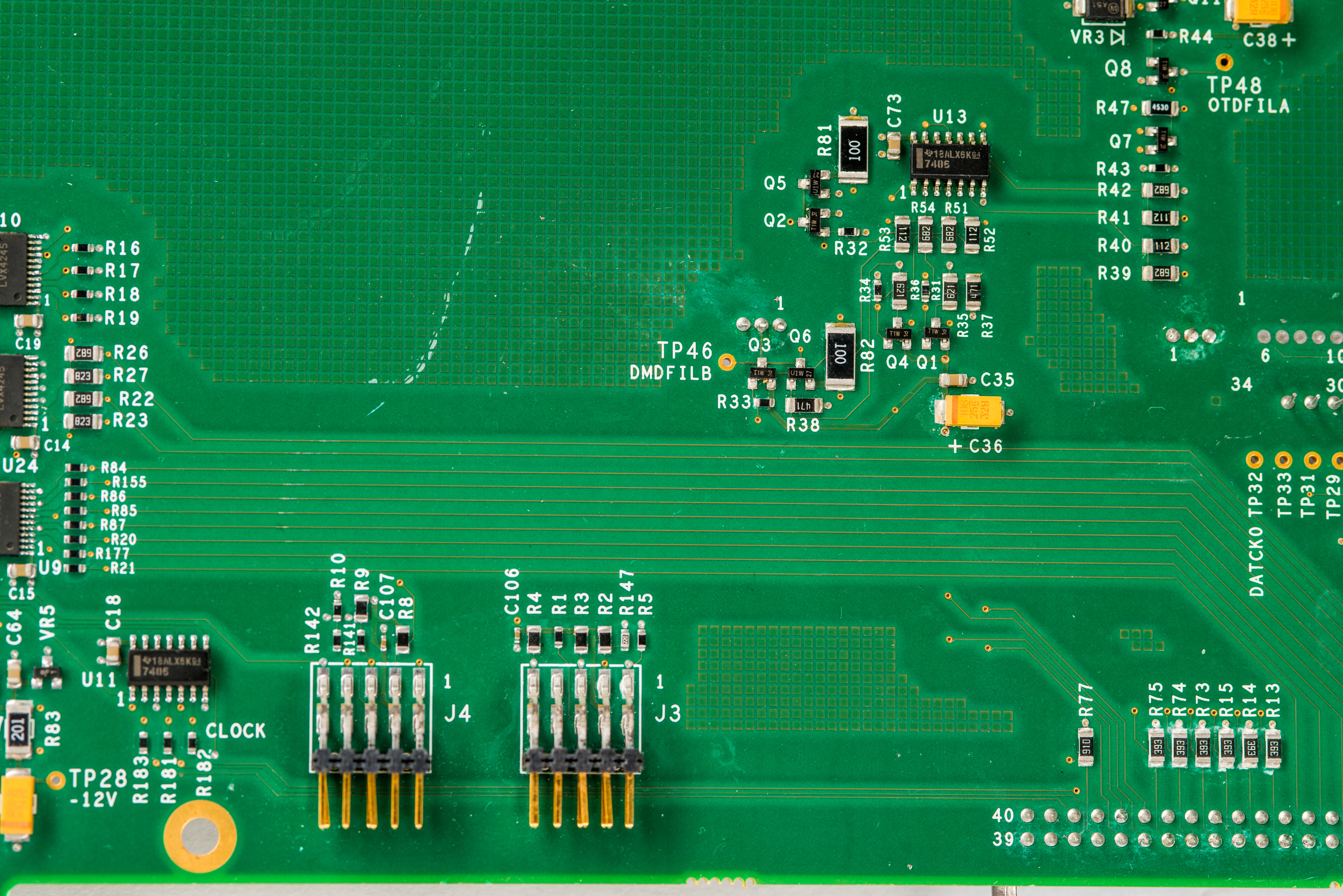
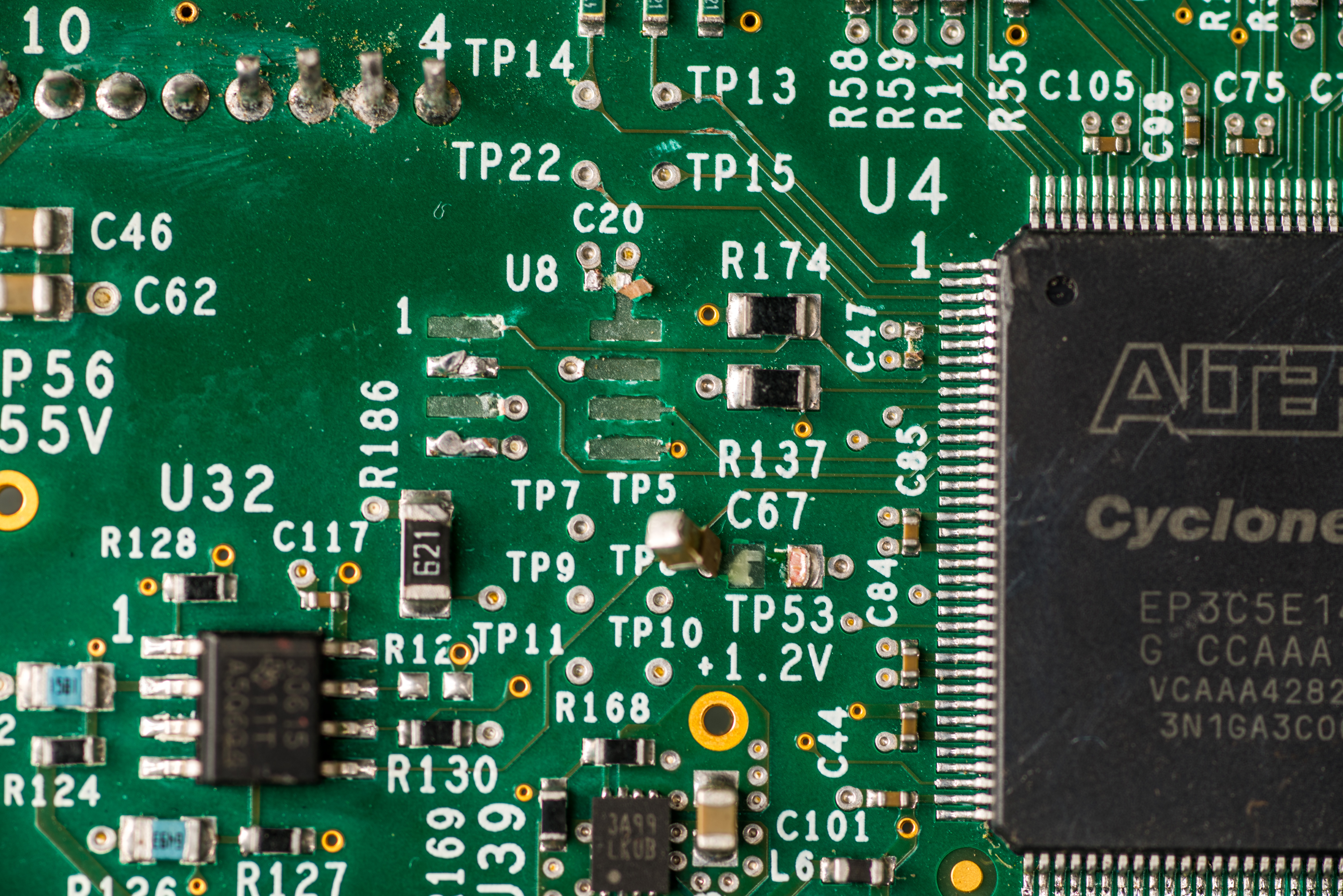
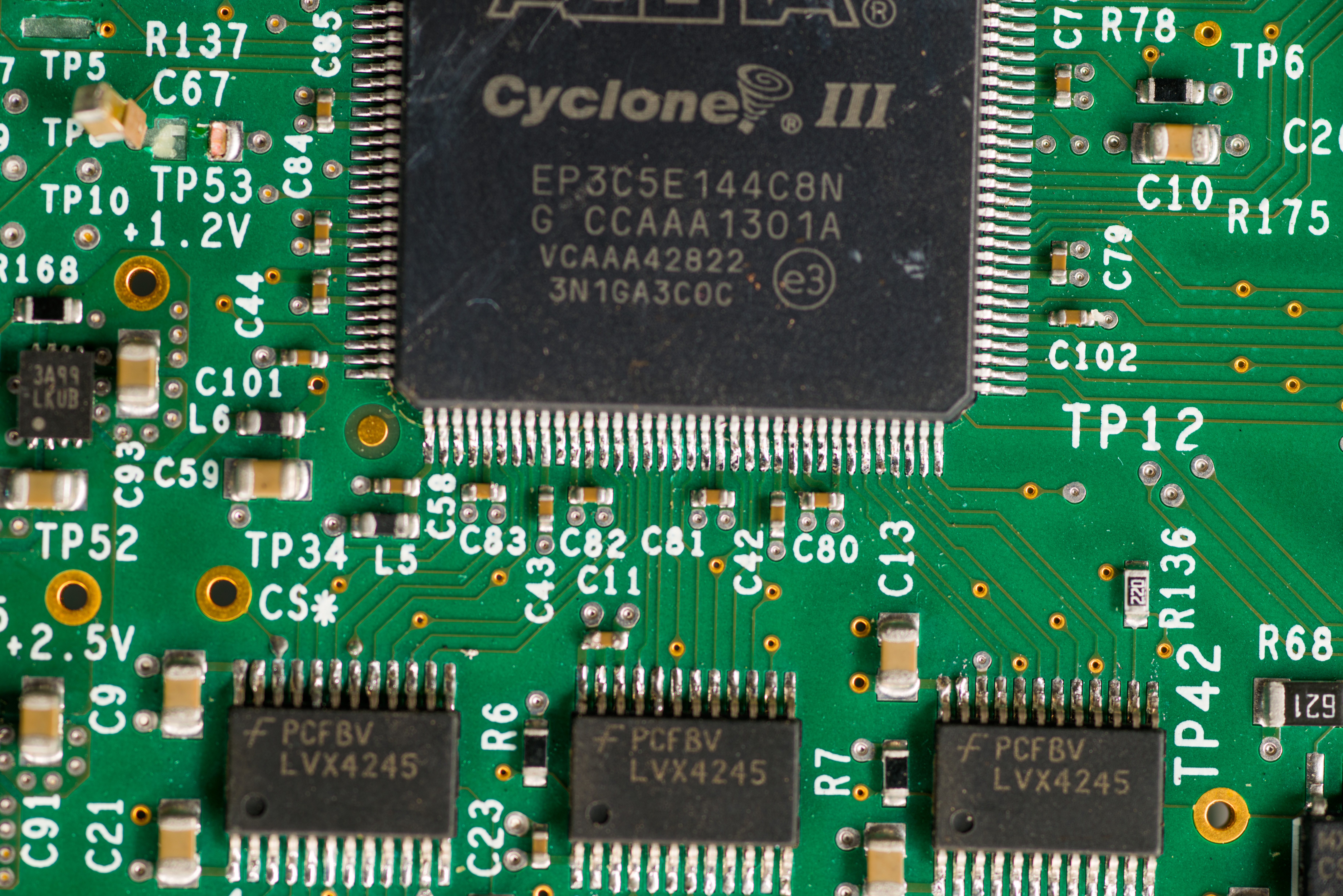
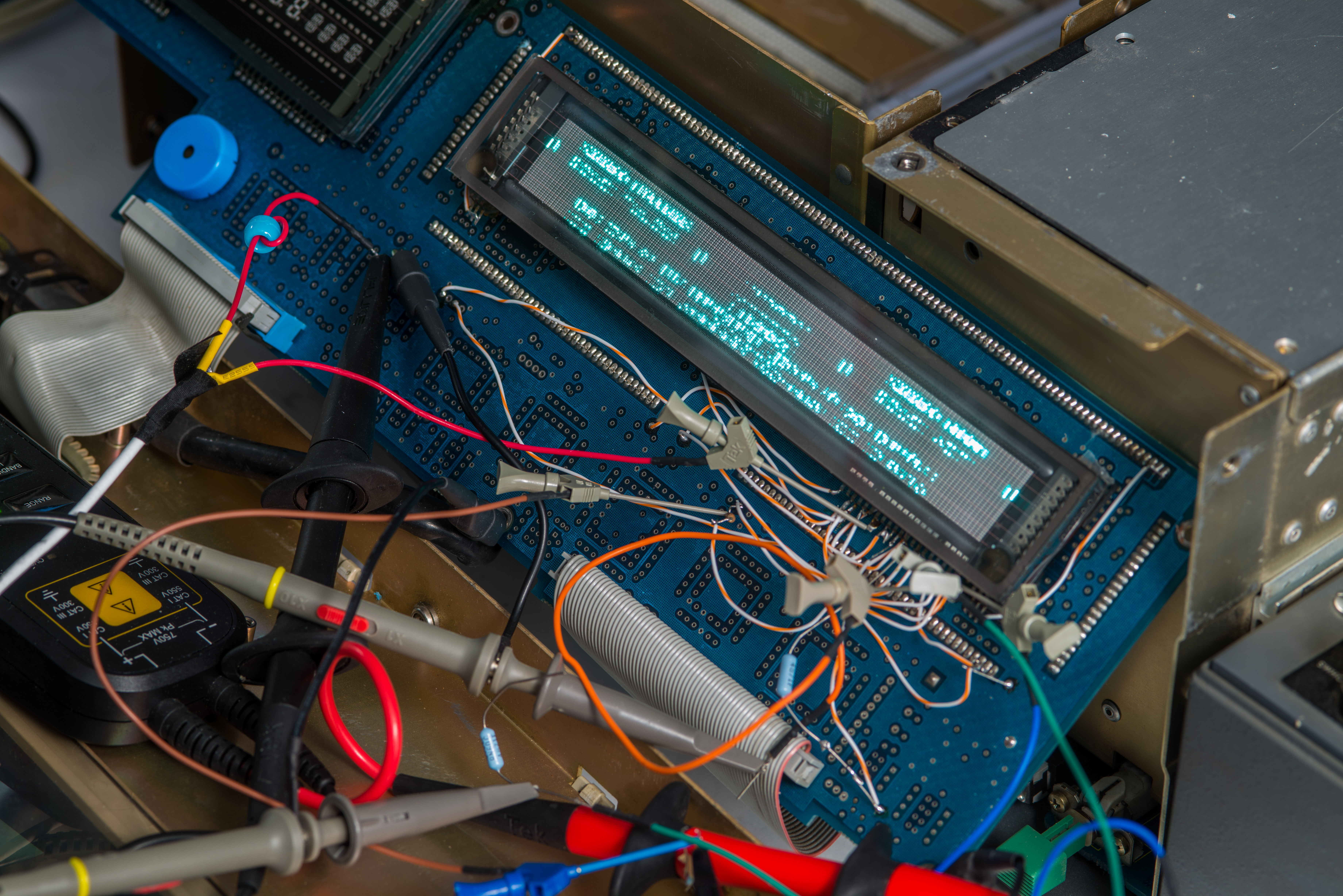
Update from April 2023. I’ve acquired yet another display board, but this time it is newer version with ALTERA Cyclone III EP3C5 FPGA.
Here are old style 1990’s (bottom) and new 2012+ style (top) display boards, designed for Fluke 5720A and newer 5790A instruments. Both boards have good glass with intact vacuum and good getters.
Higher resolution photo of newer A2 PCB:
Never mind visual artifact on the right screen, it is just stitching artifact of panoramic photo.
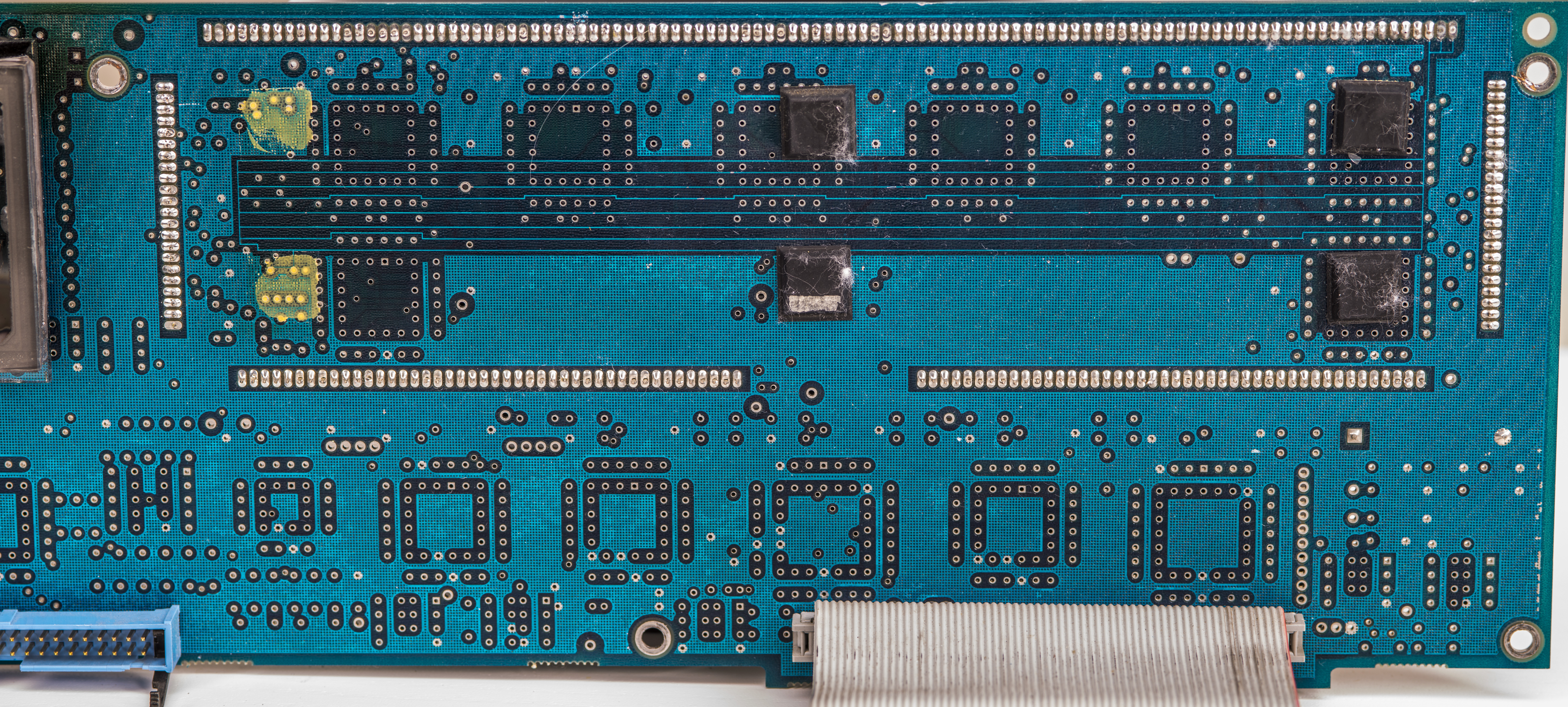
Back side reveals significant difference, especially for the right 256×32 dot-matrix VFD glass. Whole bunch of 13 custom logic chips and 8 high-voltage segment drivers are now replaced by single ALTERA Cyclone III 3.3V FPGA with 5k logic elements and some level translation buffers around it.
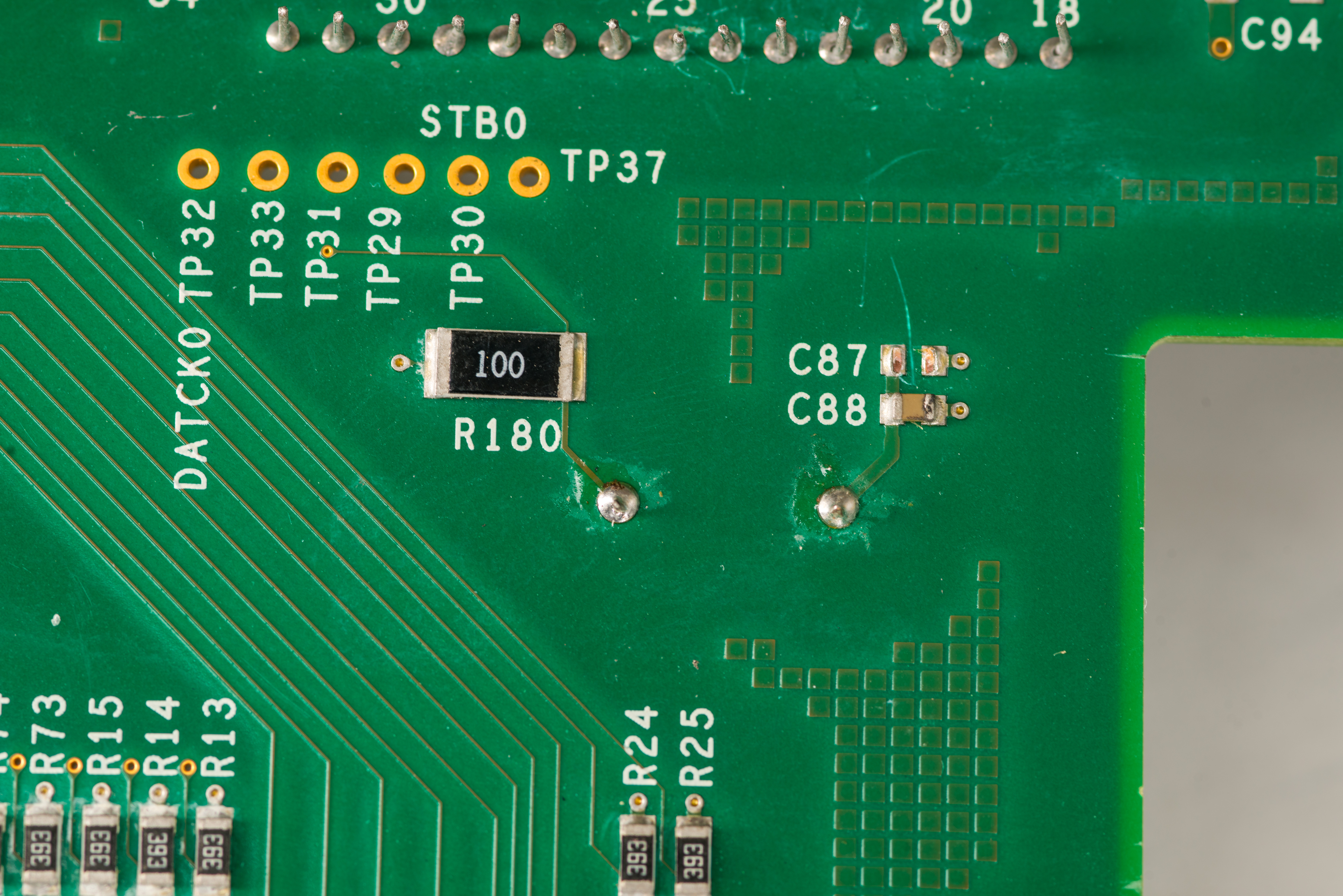
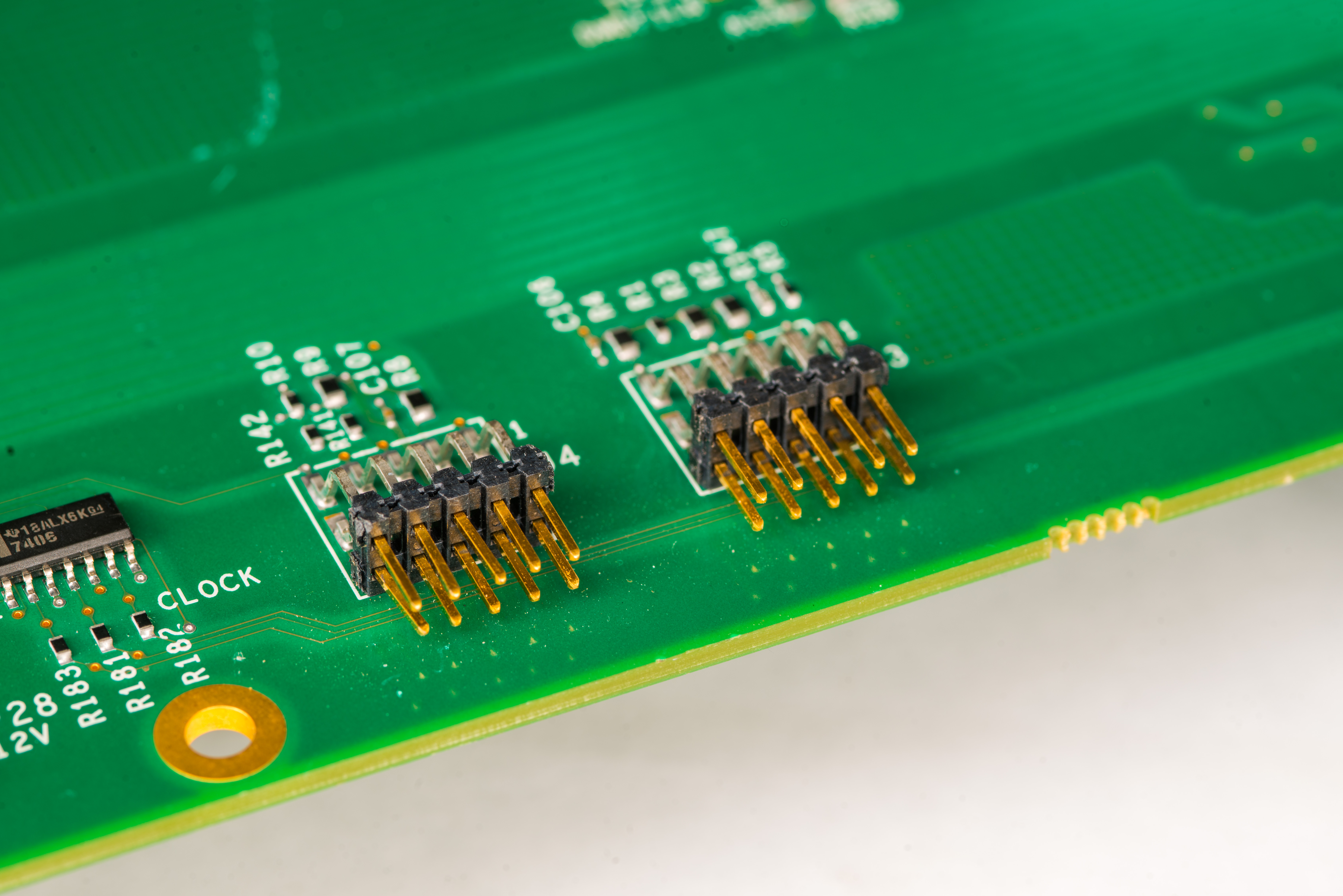
Additional connectors J4 and J3 are added to support onboard programming and debugging of ALTERA FPGA logic. I’d expect pinout for these two 10-pin 2.54mm pitch headers to follow standard ALTERA interface.
Left glass remained same as with original 1990’s Fluke 5700 design with external drivers on PCB. Both old and new PCBs use 6-layer printed circuit board.
But right VFD glass is now much slimmer with far less pins. This suggests presence of the integrated chip-on-glass driver/multiplexing controller.
Filament supply and high voltage is still required externally, but multiplexing is done right inside of the glass tube. This feature reduce required number of pins by significant factor, going from 240 pins to just 33.
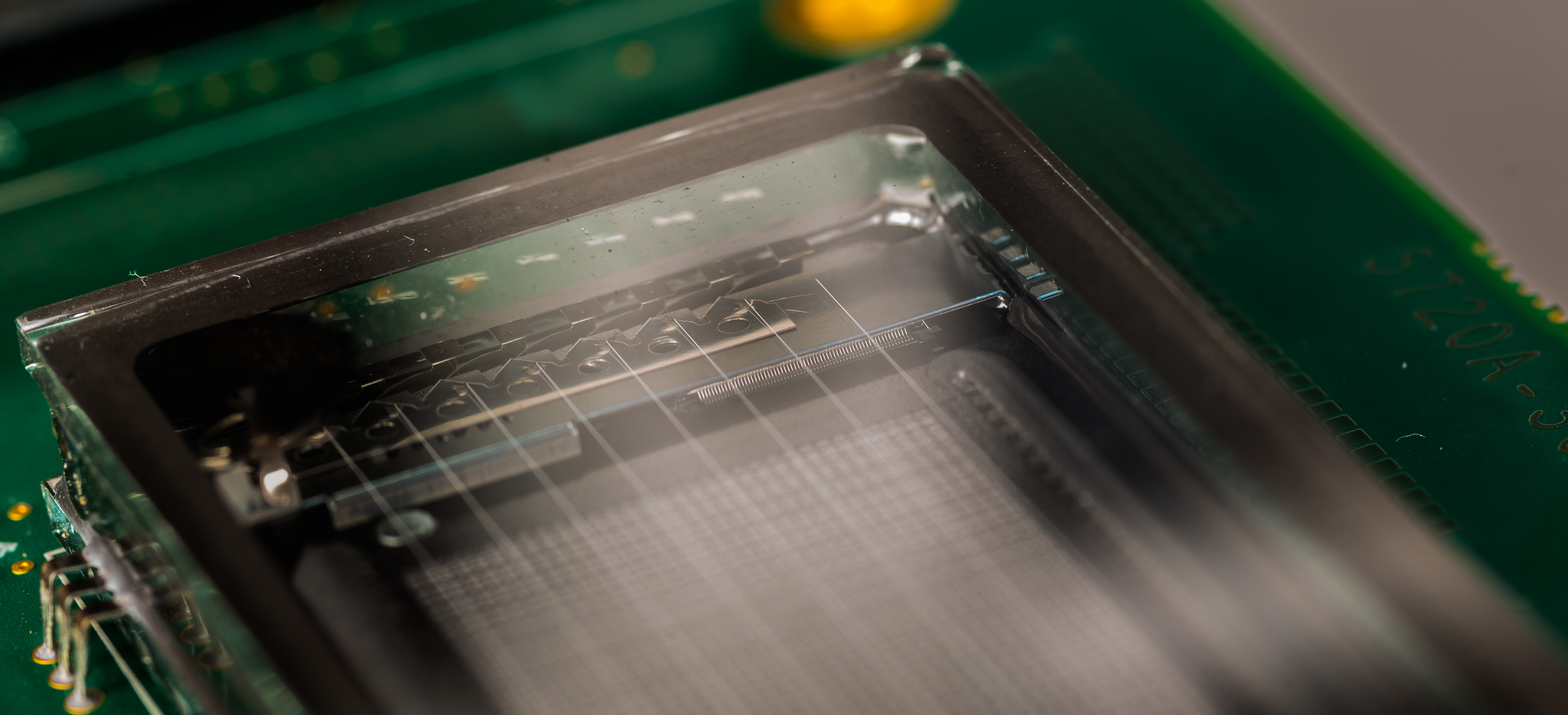
We can even see multiplexer/driver hiding under filament tensioners on both edges of VFD glass. Bare silicon die is attached to main glass substrate and wire-bonded to electrical deposited trace routing.
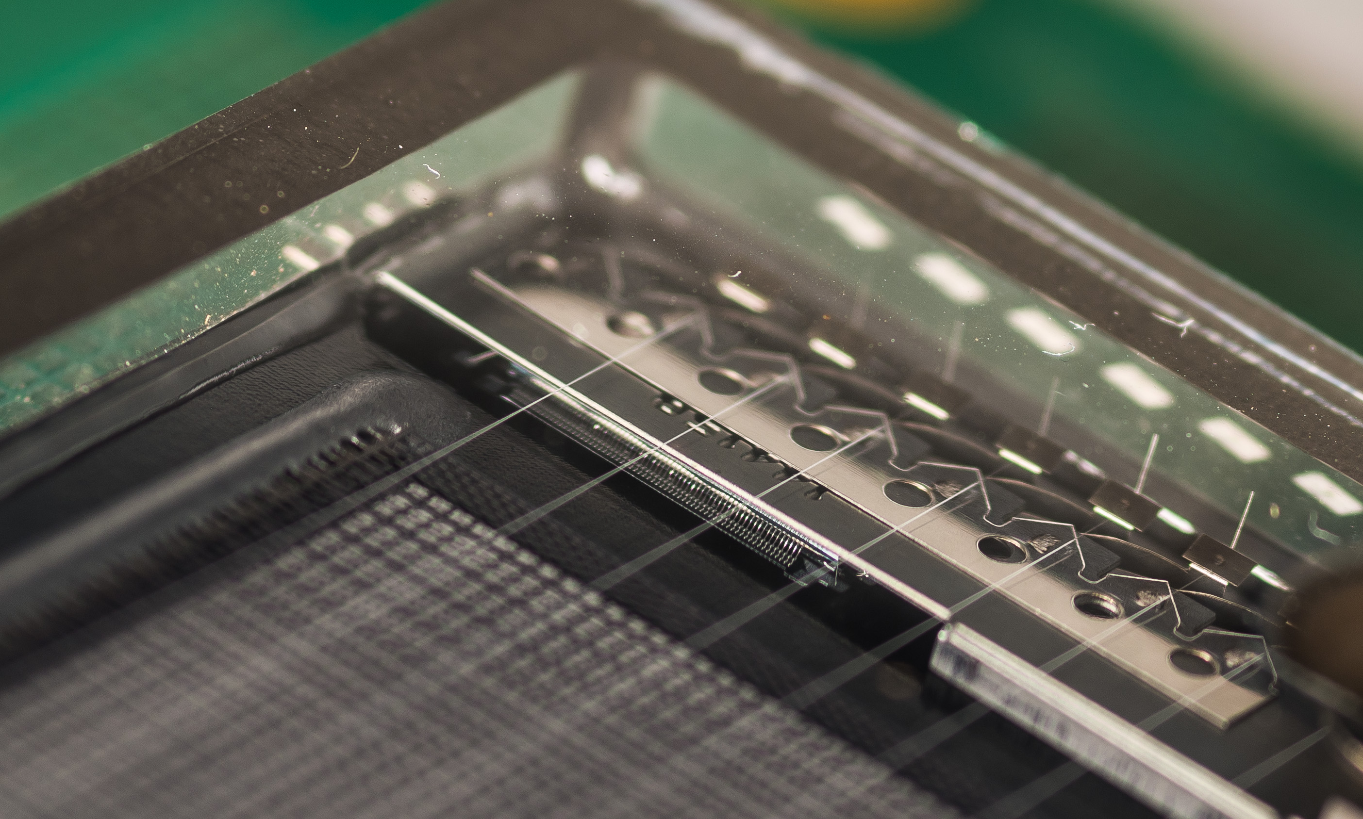
Second driver on the right side, likely same device to handle remaining section of dot-matrix array. Resolution of this display and active zone dimensions are same 256×32 pixels, just like the original Fluke glass, providing same user experience and visuals.
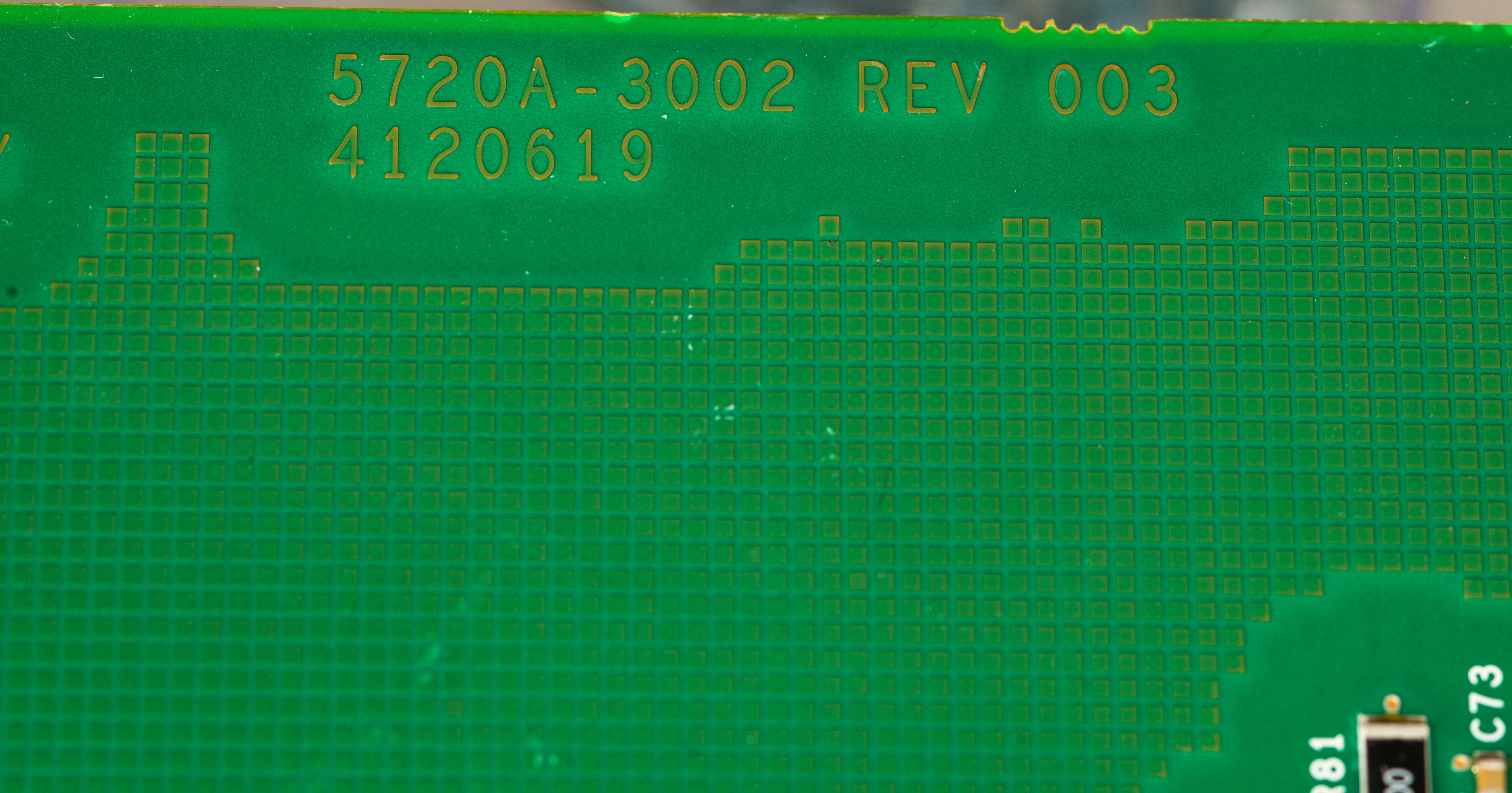
Older A2 front panel display board has Fluke P/N 761031, but this newer board sports completely different part number 5720A-3002 4120619 Rev 003.
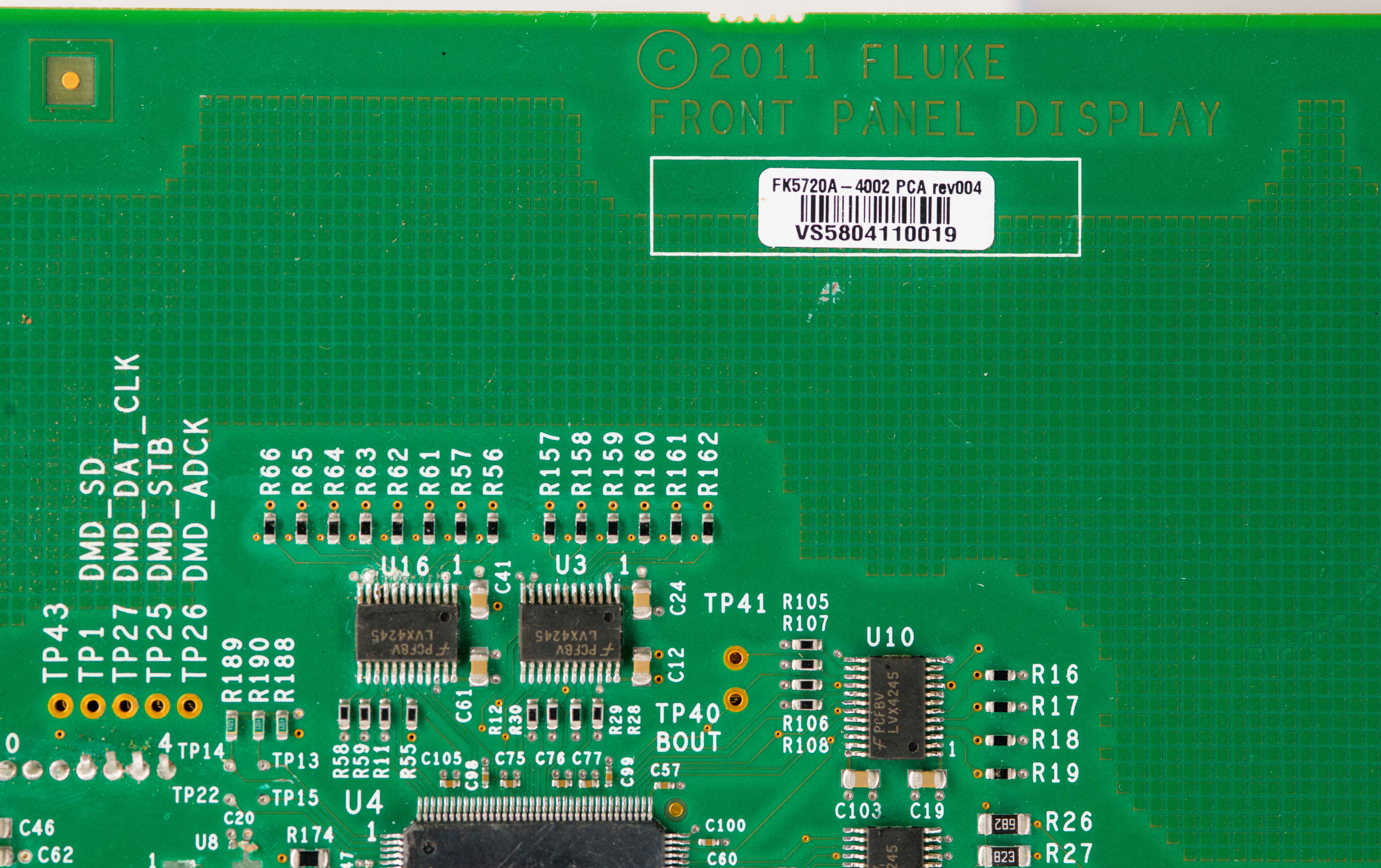
Label on newer PCB says FK5720A-4002 PCA rev004 while actual this PCB design was completed in 2011.
Connector J3 provide standard Altera JTAG port to access Altera EP3C5 configuration.
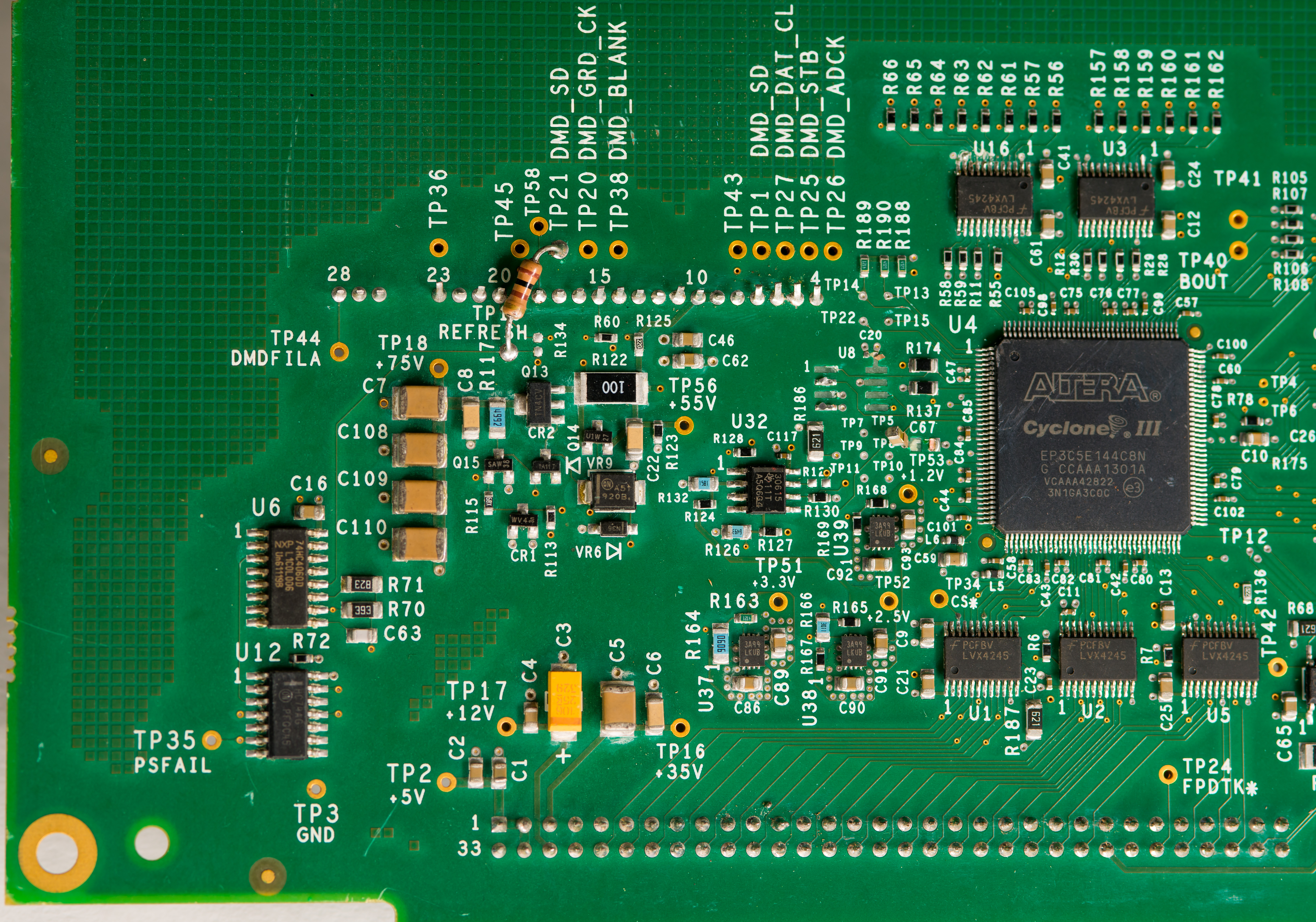
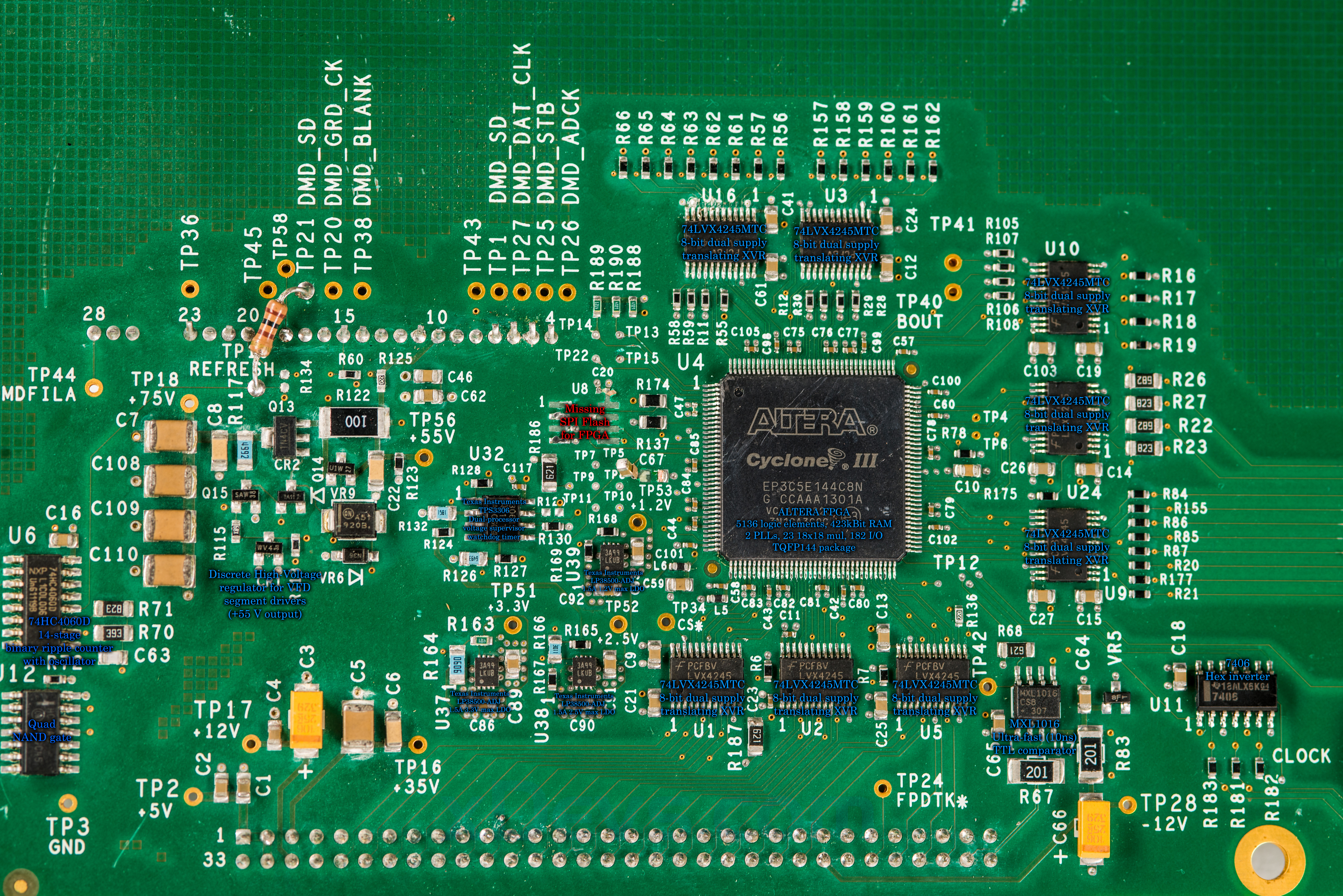
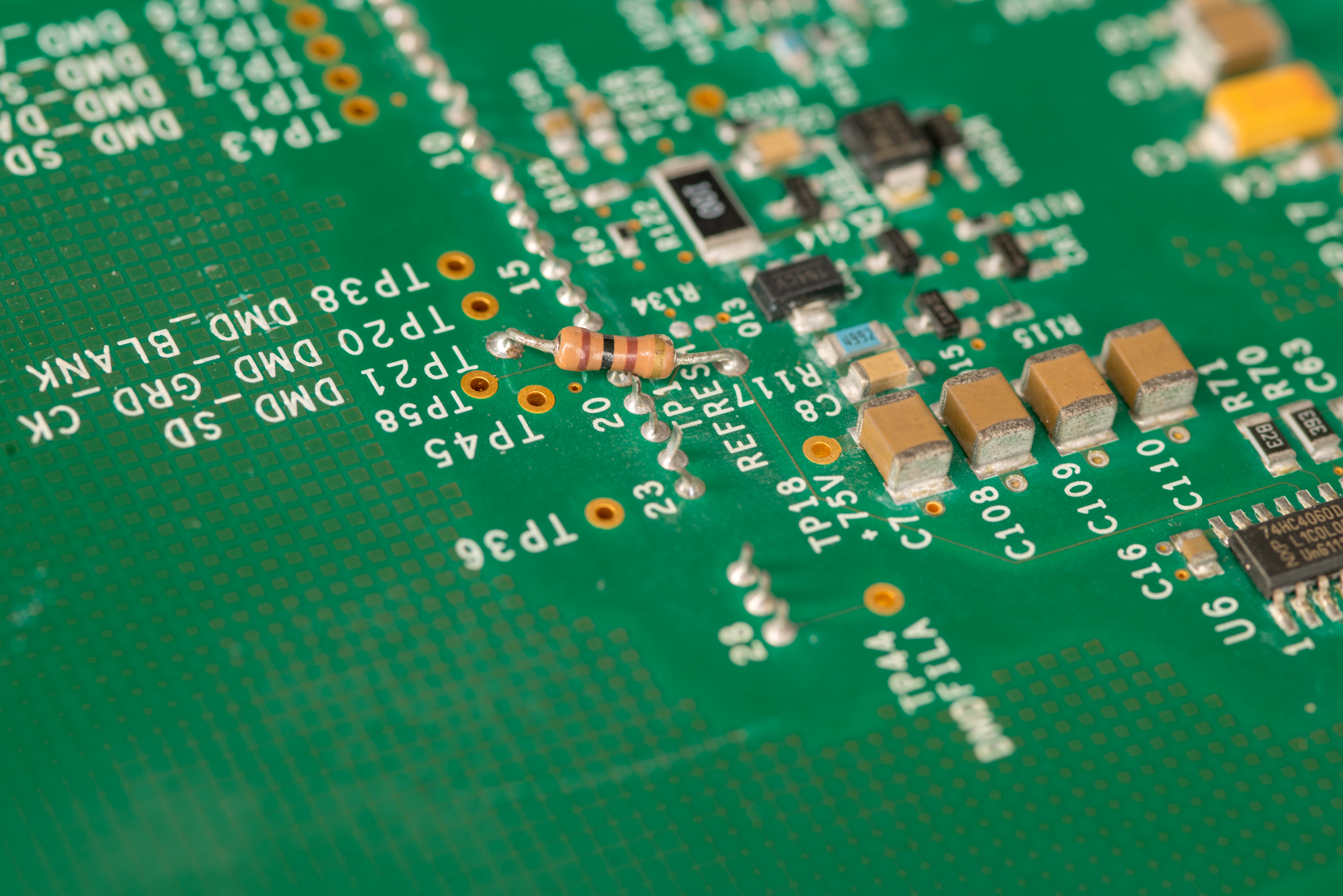
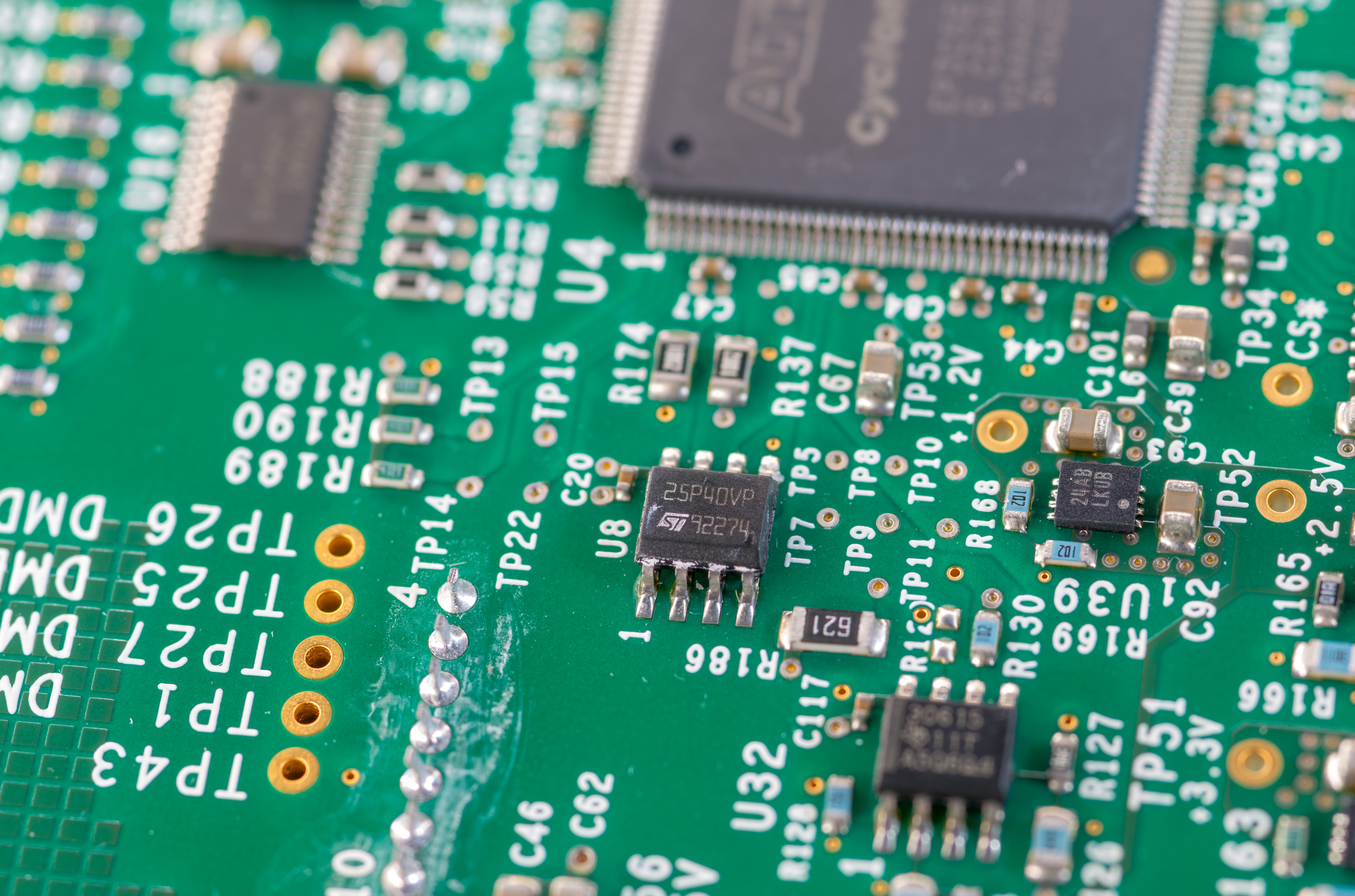
On closer inspection this newer board is sadly unrepairable without additional help. This is due to missing critical component – configuration SPI Flash memory chip (SOIC8) that supposed to be located in U8 position next to Cyclone III FPGA. Without contents of this SPI Flash memory this FPGA cannot do anything, because bitstream and actual logic design in Cyclone III is loaded upon each power up from said configuration memory.
Repairing damaged PCB hardware pads and busted capacitors is easy, but without bitstream dump from SPI Flash it’s as good as paperweight. So I’m looking now for brave soul that have 5720A with such newer FPGA-based front panel PCBA and familiar with FPGA programming tools such as ALTERA USB Blaster to dump the contents. There is small chance that Fluke protected design from reading out, but most likely it is still unlocked and can be easily readout externally with standard JTAG port access. Until then, this board is pretty but useless.
I cannot replace the VFD glass to older board either, because newer 2012 VFD has different interfacing with integrated drivers and just few pins, not like older front panel glass that is just array of segments routed to 240 external pins. This new glass is likely the same as GU256×32-800A display from Noritake.
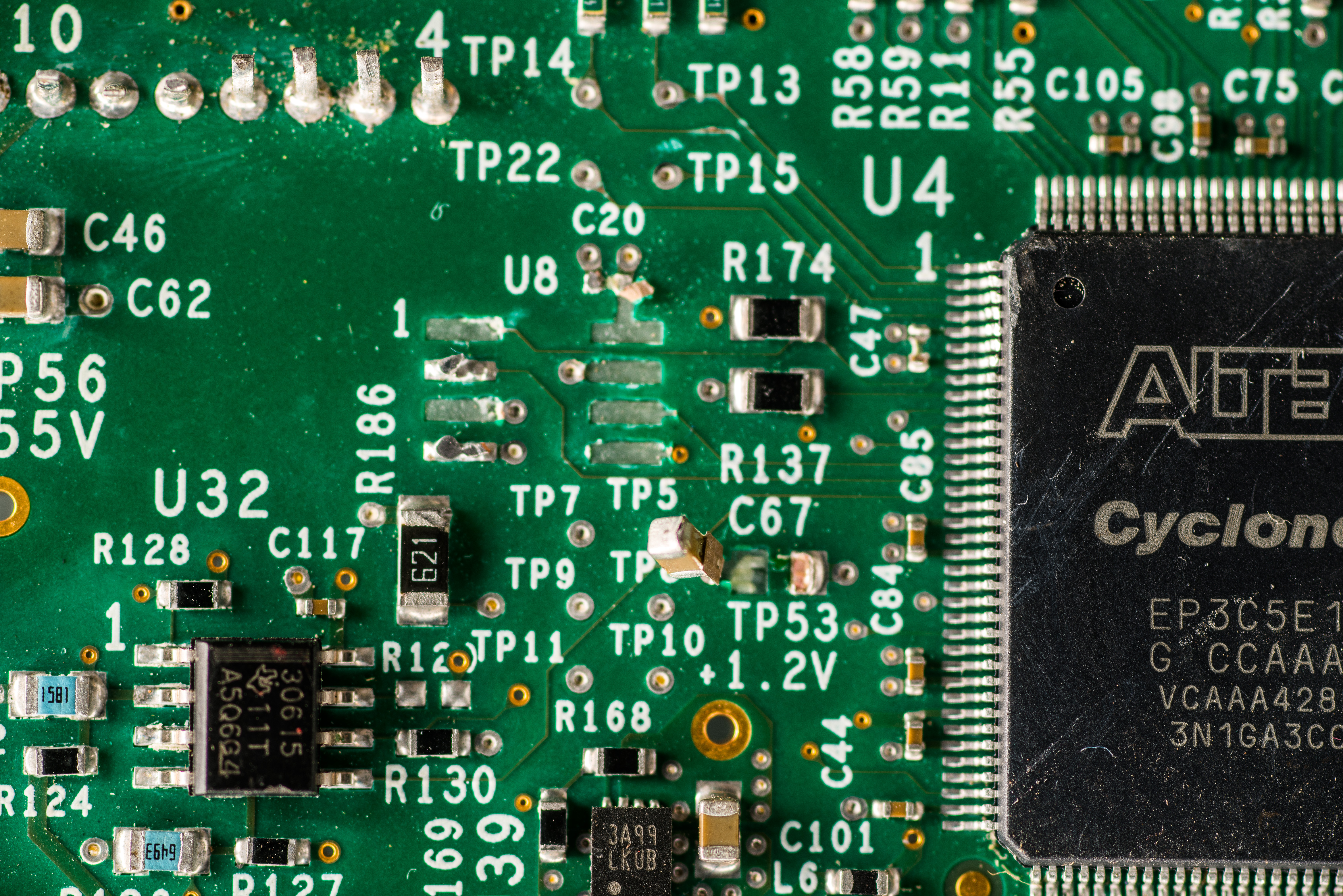
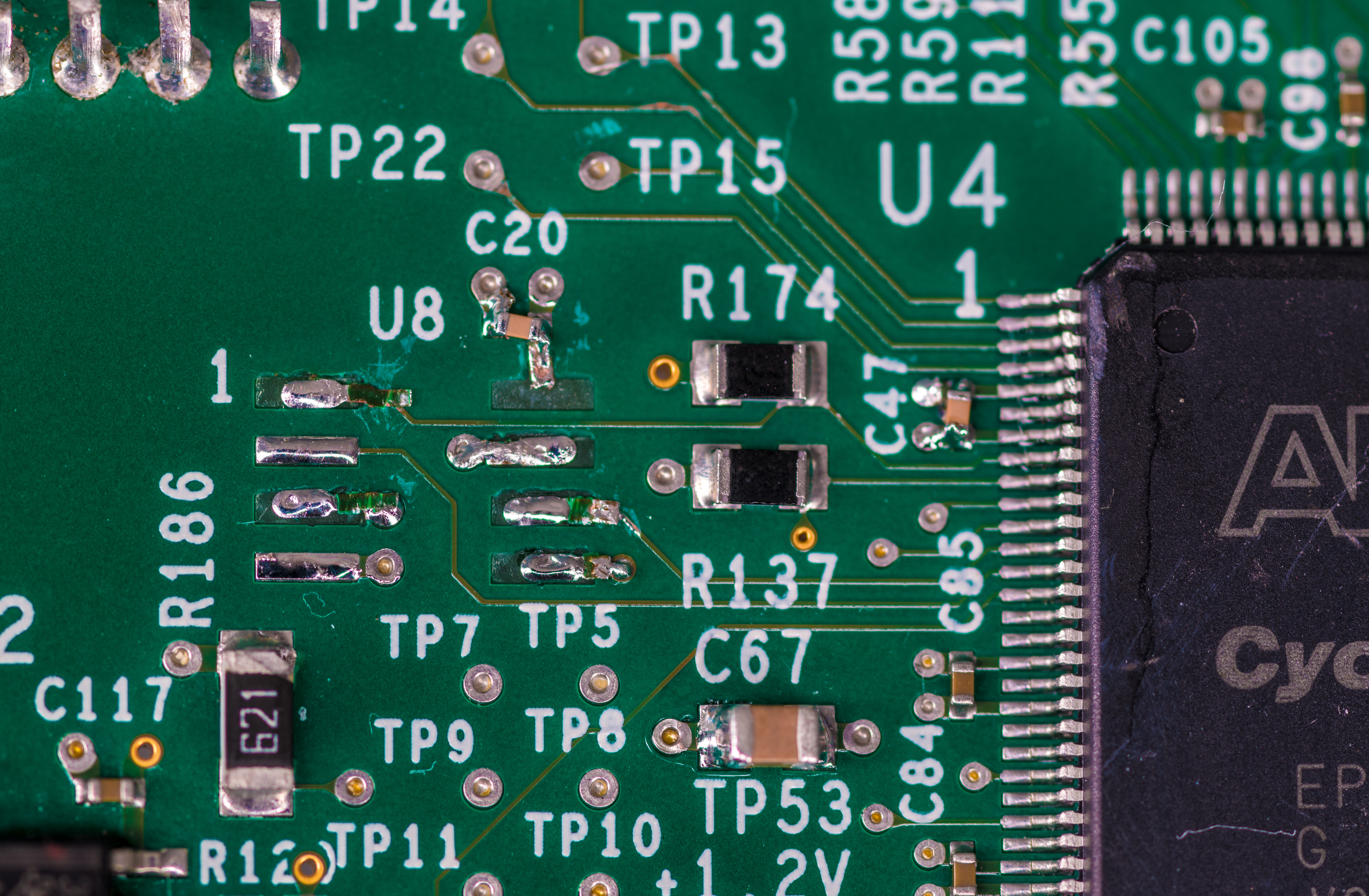
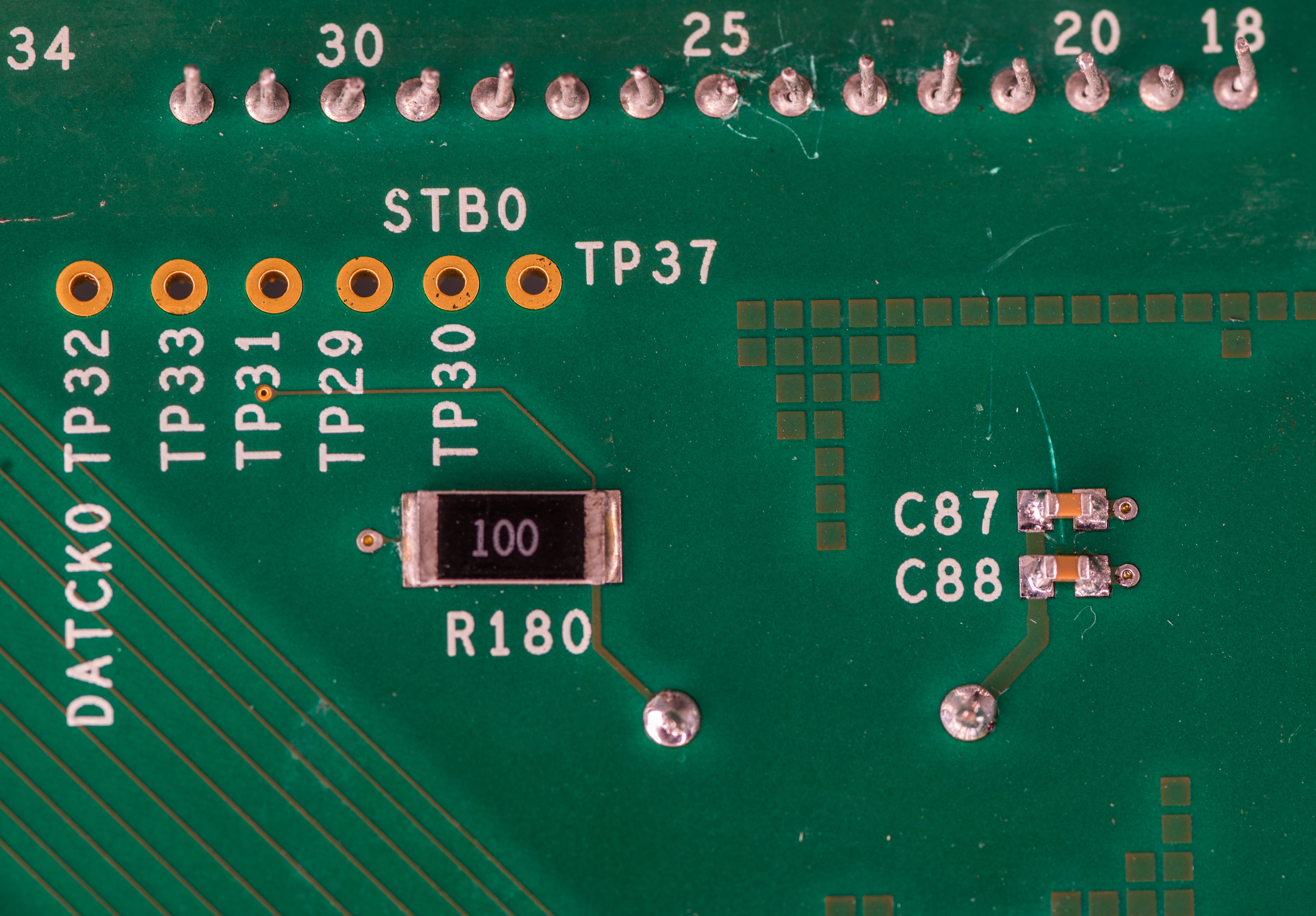
Poor ceramic capacitor is still hanging on remains of copper trace next to destroyed position for SPI Flash U8.
C87 is also destroyed by something sharp. C88 is in place still but also cracked and likely shorted. Both of those will be replaced.
Pins on EP3C5 FPGA were also mangled with solder a bit, so perhaps somebody was trying to probe something or repair?
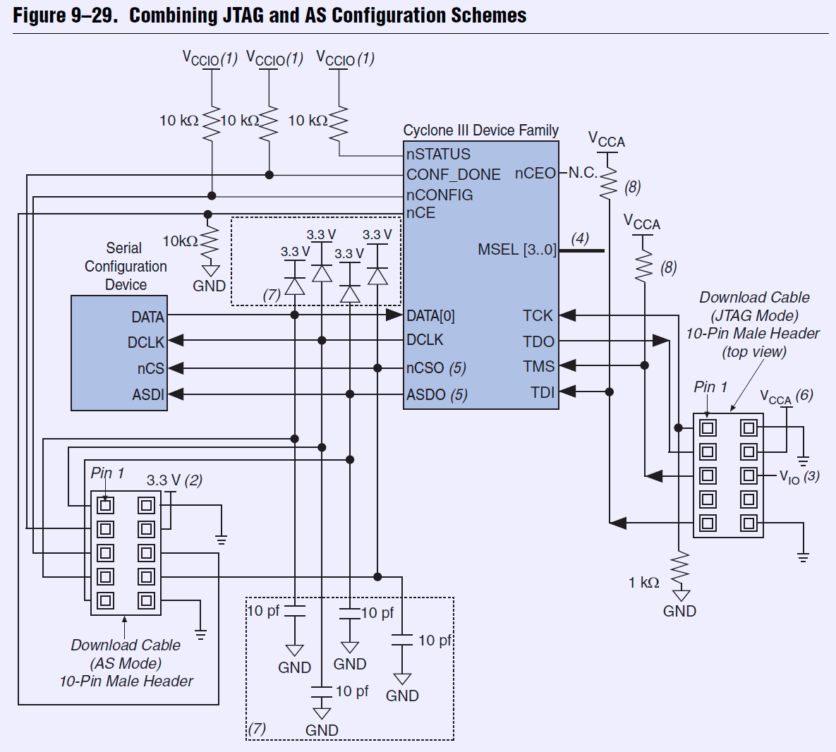
Expected signaling for J4 and J3, based on Cyclone III Device Handbook manual, page 9-57
I can solder back SPI Flash chip, power up the display board with just logic +5V supply and check if I can access ALTERA FPGA from USB Blaster programming tool.
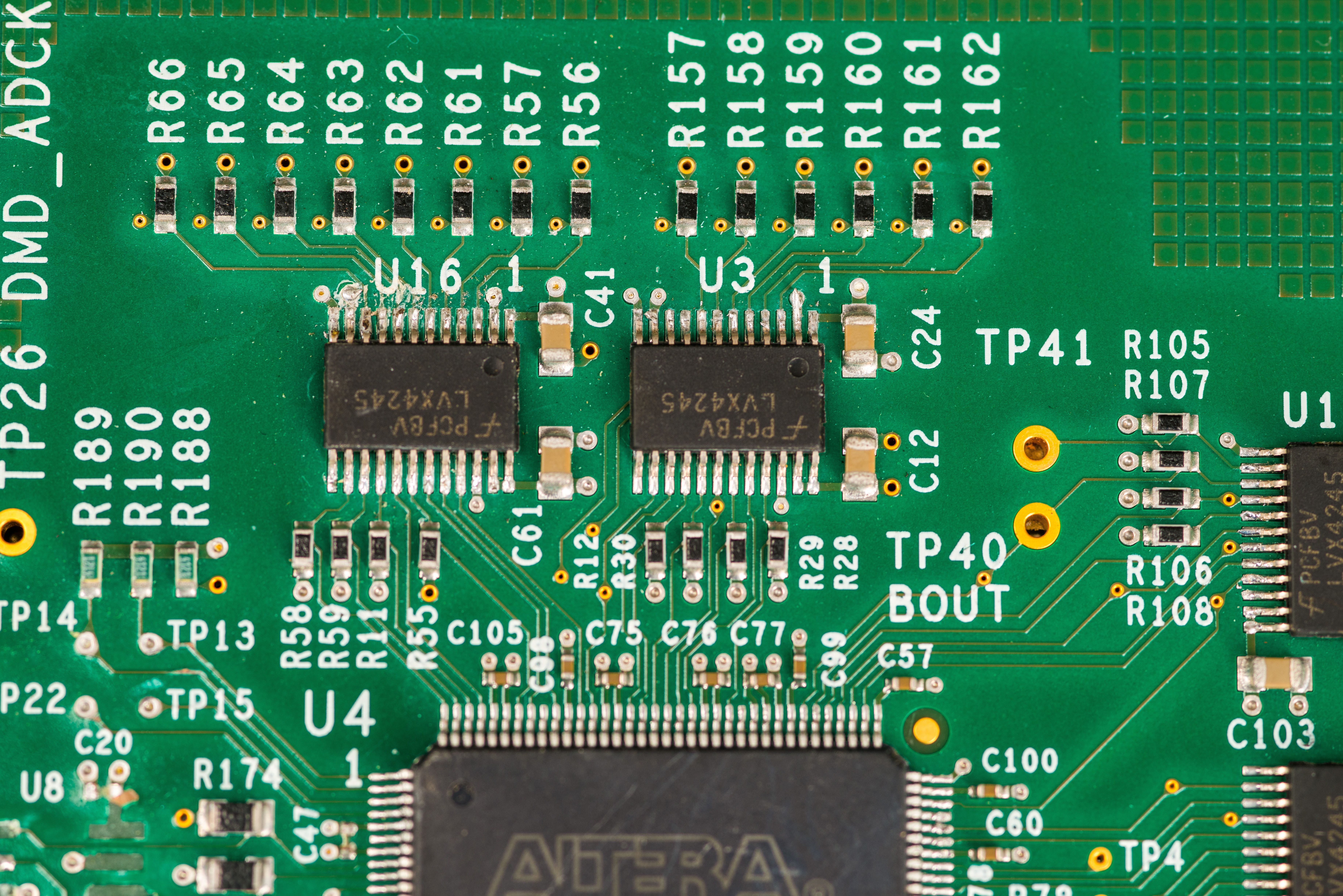
There is some white residue dirt around U16 level shifting IC, PCF LVX4245
Repairs for new A2 hardware in hopes to obtain FPGA bitstream in future
Before installing replacement SPI Flash chip on U8 position I have restored missing pads and connections. With microscope, ERSA Icon fine tip soldering iron and steady hand I’ve put pads cut from some donor Tektronix DPO4034 PCB. Configuration flash ALTERA EPCS4 in SOIC-8 was also salvaged from oscilloscope board, because it is long obsoleted part today.
This took about 60 minutes to complete. Once pads are installed, I’ve put back C67 (10 µF 16V 0805 ×7R capacitor) as well as two 47nF 16V 0402 ×7R capacitors on positions C20 and C47. R186 also have mechanical damage but I will deal with it after I get actual bitstream for this front panel assembly.
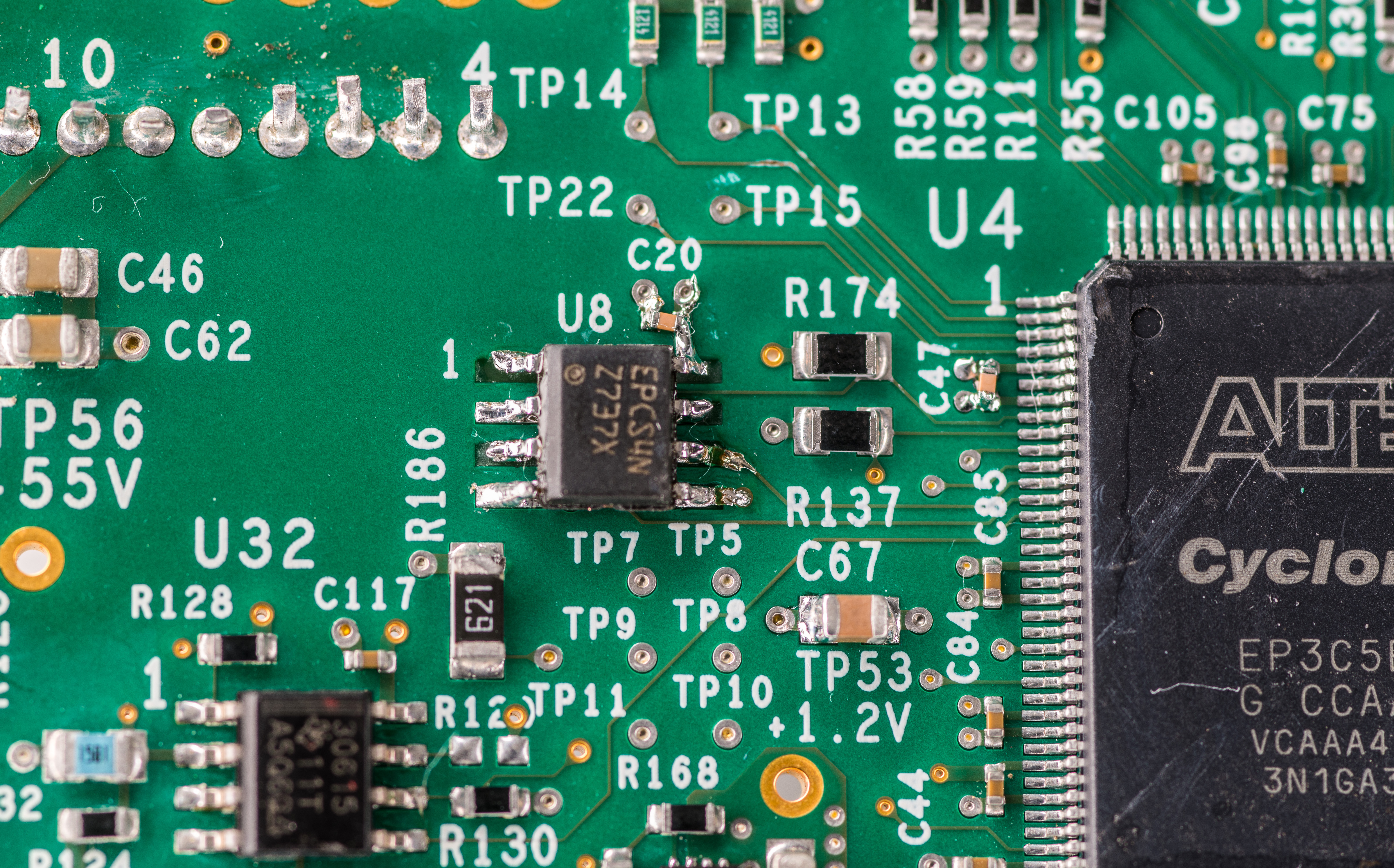
SPI Flash was carefully soldered on top of restored pads and all connections to FPGA pins were probed and confirmed good.
Pair of 100uF 0603 ×7R capacitors were installed instead of busted C87 and C88 for the buzzer.
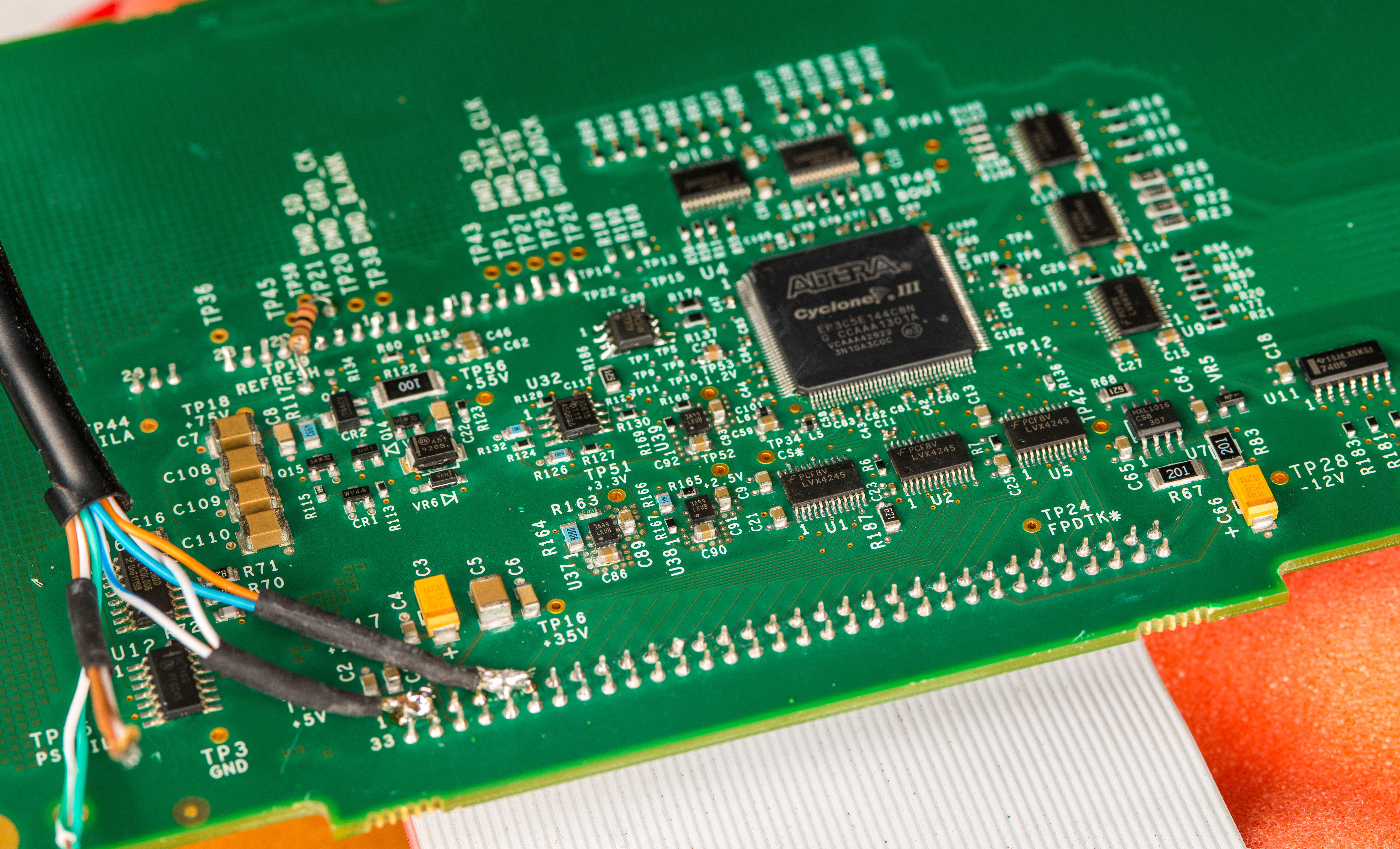
Now we can power up and check if FPGA at least responds. Actual 5700/5720A calibrator supplies bunch of voltage rails to A2 PCBA like +5V, +35V, +75V, filament AC voltage, +12V and so on. It could be dangerous to have all power rails present without proper configuration in ALTERA (now part of Intel PSG) FPGA, so I’ve connected only +5V rail to Keithley 2400 SMU instead of risking more damages on calibrator hardware.
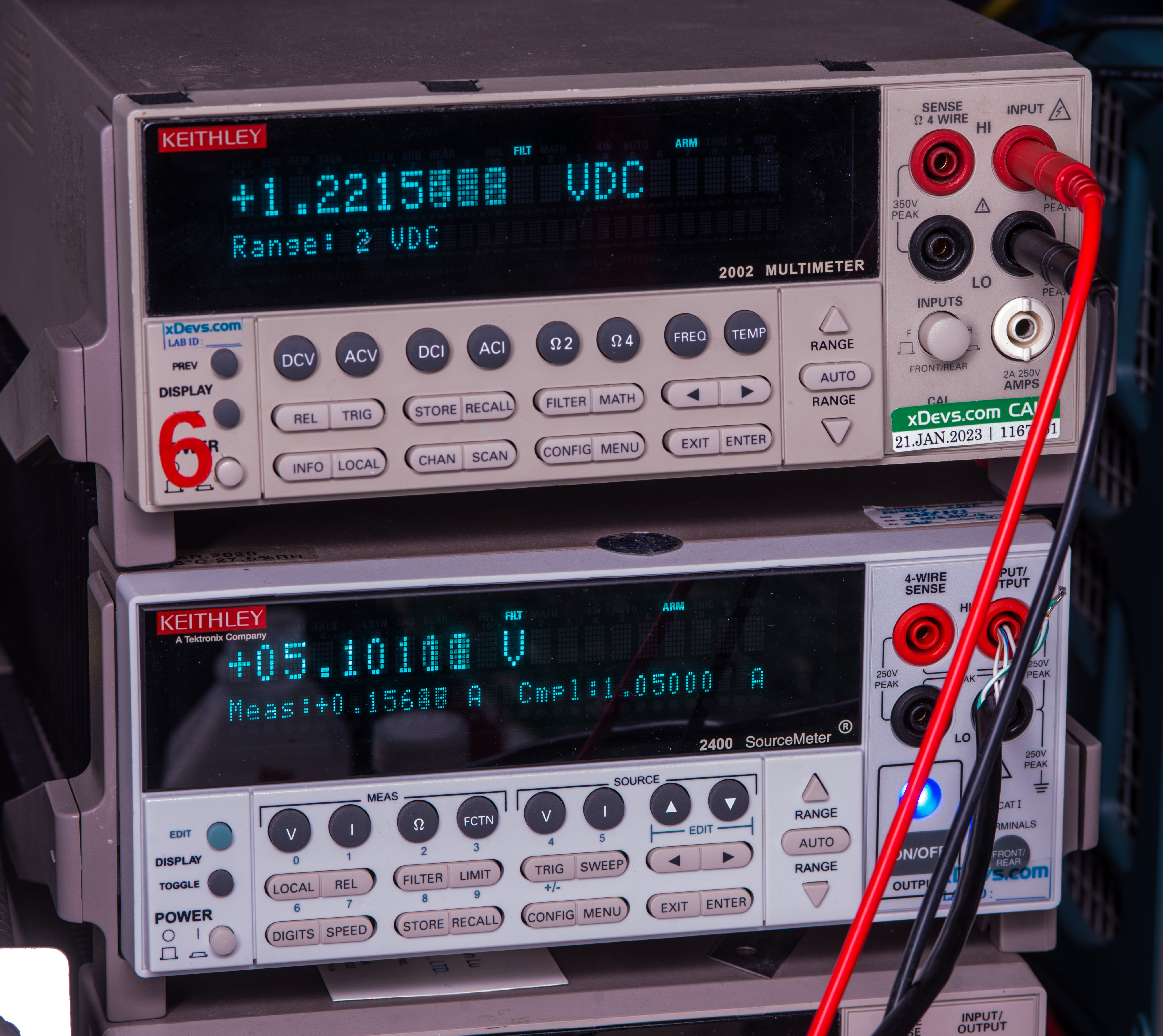
On power up from +5.1V sourced by SMU current draw starts at ~0.2A but quickly drops to around 0.17…0.16A which sounds reasonable. Onboard linear power regulators that supply voltages to FPGA were checked and confirmed healthy +3.3, +2.5 and +1.2 VDC outputs. Nothing on the board sizzle, which is always a good start.
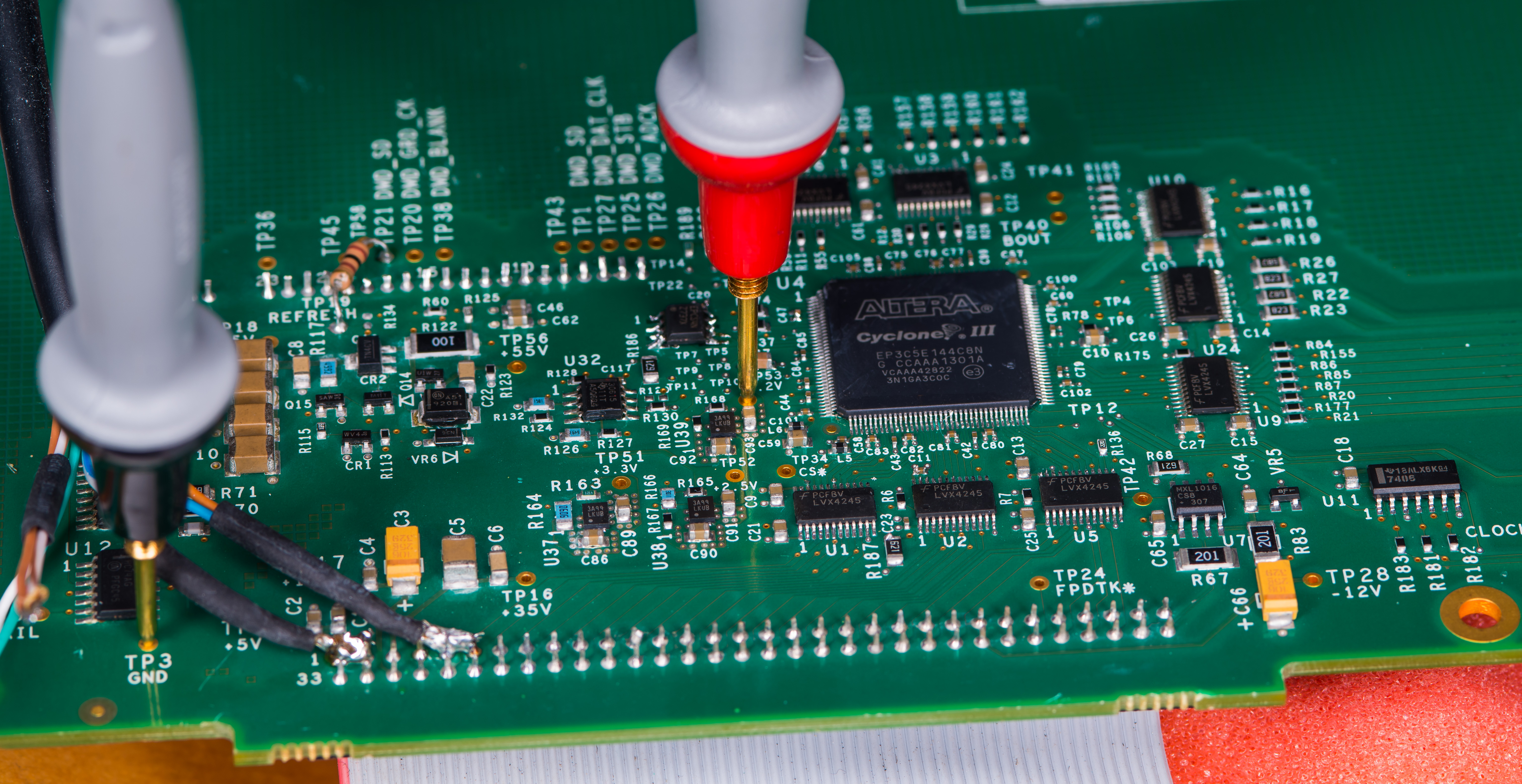
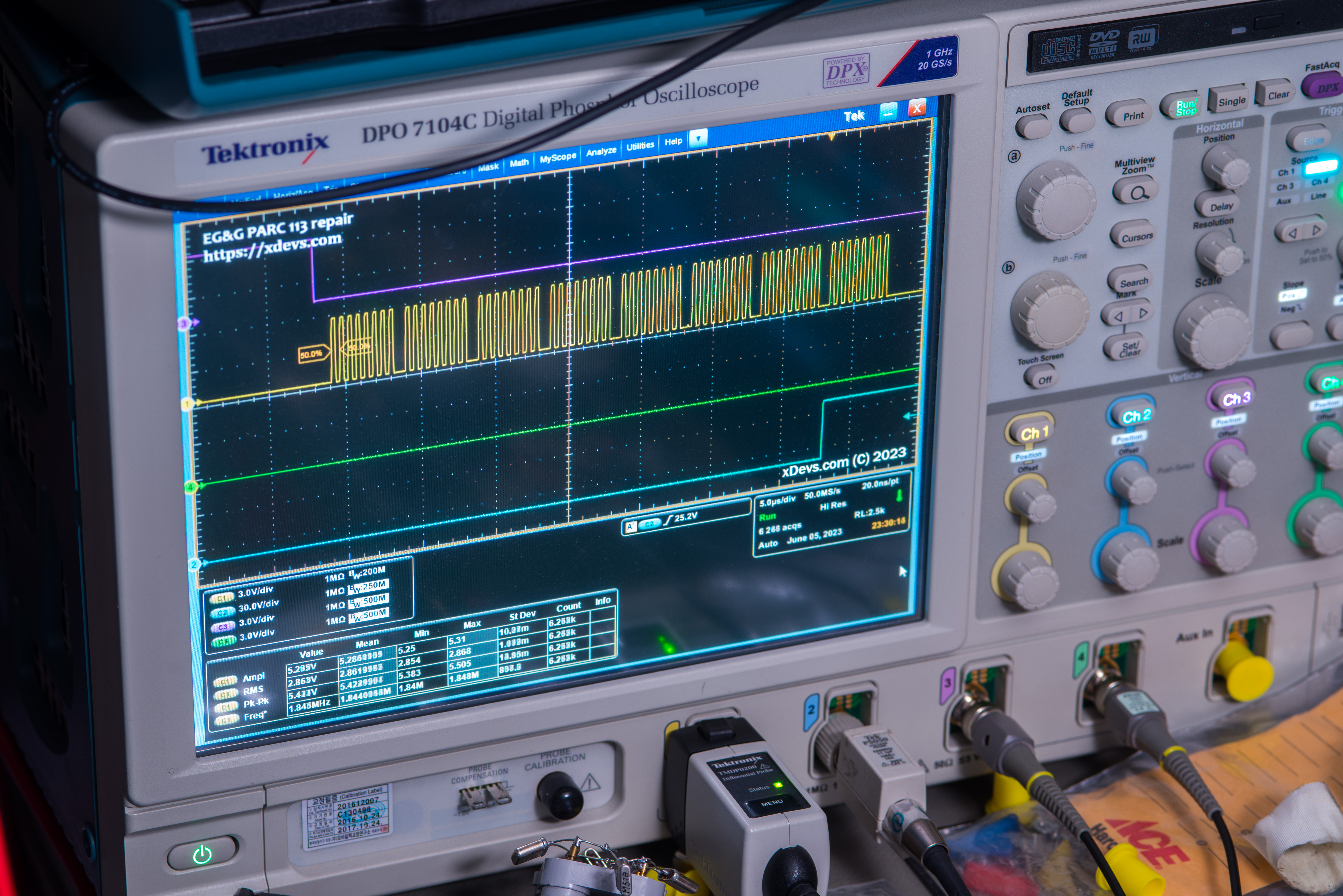
Time to connect JTAG to the board and see if we can detect Cyclone III from programmer. To test communication I’ve used USB Blaster from the Terasic devboard and Quartus 15 Programmer tool. Experimentally I’ve determined that J3 header is actual JTAG port with +2.5V I/O voltage level, and J4 is something else with +3.3V voltage level.
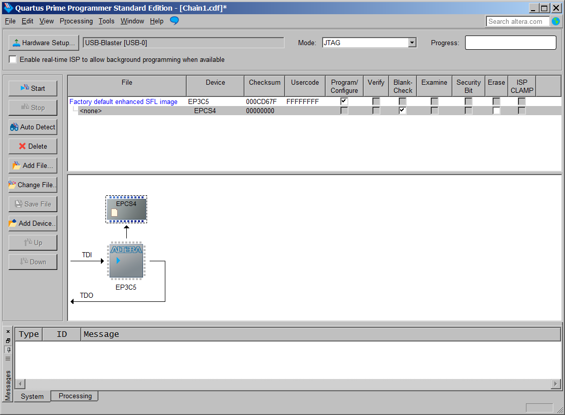
Autodetection with Quartus Programmer correctly found and identified EP3C5 device. I’ve added EPCS4 flash chip into the chain and attempted to check if it is blank.
![]()
This EPCS4 already had configuration data in it for Cyclone II device, so testing for blank resulted expected fail. This meant that chip is not empty.
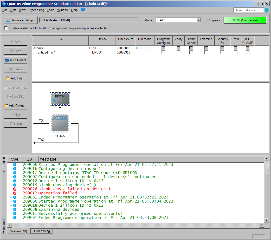
Examining contents allow to reads bitstream out of the EPCS4 and store it in Altera-specific JIC binary file, if configuration memory is not read-protected by manufacturer. Hopefully I can obtain and use such JIC-file to write my own EPCS4 if I can obtain the dump from working modern Fluke 5720A A2 board.
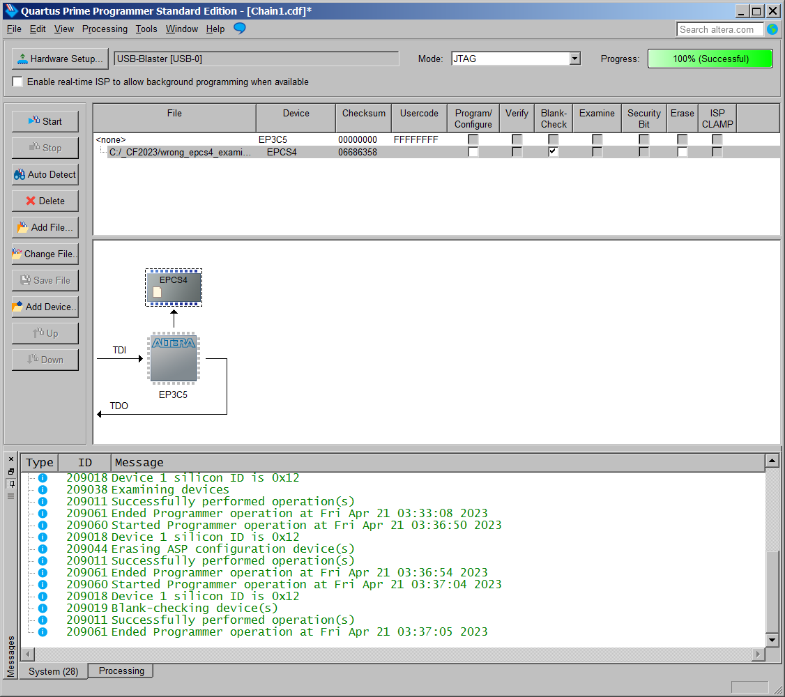
Also erasing my EPCS4 worked fine without surprises. Now I can only wait and hope for helpful owner of such newer A2 PCBA, to recover the correct dump.
Testing with new A2 hardware
Attempts to get new glass with integrated drivers working on old front panel electronics (by reusing input to drivers from logic chips and powering new VFD glass from external +55V source) ultimately failed due to different anodes mapping. For tests I’ve obviously removed original high-voltage drivers from PCB and instead routed serial data lines from onboard logic to same test points on new integrated glass.
All signals are +5V level and looked reasonable on the oscilloscope. In best case all I got was just barely recognizable screen data, heavily garbled.
Old drivers topology was configured to drive A+B and C+D anodes together, while new CIG glass is operating with A+D and B+C anodes grouping. Also mapping of bits is different.
So reusing newer glass with integrated drivers on old PCB is impossible as result due to this different protocol and mapping.
Return to original plan A with recovering bitstream contents. Thanks to friends and their support I’ve repaired one of Fluke 5790A AC voltmeter standards. It was old unit from 1992 but had front panel replaced at some point later. Lucky for me new front panel was the fancy new FPGA version.
Fluke used 25P40 SPI ROM to store ALTERA Cyclone III FPGA configuration. With help of USB ByteBlaster connected to J3 JTAG port I’ve examined and stored bitstream from the good front panel board. To avoid damaging electronics while accessing JTAG (as we have +75V, +12V and +35V coming from the calibrator mainboard normally) I’ve powered only +5V from HP 6629A power supply, current limited to 500mA. Actual consumption on this rail was just 180mA, which is reasonable for Cyclone III FPGA and various chips around.
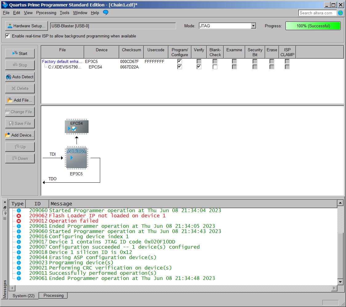
Fluke 5720/5790A front panel FPGA bitstream backup, checksum 0×0667D22A
Now with bitstream I’ve reconnected JTAG to broken board, flashed EPCS4 device on it and put back integrated driver glass that was previously de-soldered from the failed attempts with old FP PCB board.
To my satisfaction board booted up and calibrator properly recognized front panel, which confirms successful FPGA configuration and function. However bunch of segments on BOTH good left segment glass and unknown dot-matrix right glass were missing, and 5720A upon power up complained of “control display failure”, but proceeded to boot anyway.
Touching up solder joints at FPGA and buffer chips didn’t change anything. All voltages were measured within expected specifications. Issue with both displays hinted that it must be some connection or data integrity issue. And since there is wide parallel bus between front panel and motherboard with main calibrator CPU perhaps one of the signals is missing/shorted? And FP board did not provide correct data back to main CPU, hence it detected fault, which should be somewhere between FPGA and main CPU, and not the VFD glass side. Pondering a bit more with multimeter revealed indeed open wire in the 64-pin ribbon cable to mainboard DIN connector.
After replacing whole ribbon cable to one from the old A2 front panel I’ve got now nice and fully working modern A2 board:
Now Hulk-3 calibrator officially have both displays and fully operational “head”. Front panel plastic is very ugly looking, but I’ll worry about cosmetics much later after electrical functionality is restored.
Another A2 older style PCBA test
While at it I’ve also tested another older version A2 board, that has some bent pins from the right glass display.
After cutting and fixing that issue board powered up and confirmed working. Brightness of the segments is quite alright for 20 year old VFD.
Calibrator that originally had this display on was operated mostly in remote GPIB control mode, which caused sentence “Operating under REMOTE control* to be burned in right screen. This is common for decades old displays on all Fluke 5700/5720/5790A calibrators.
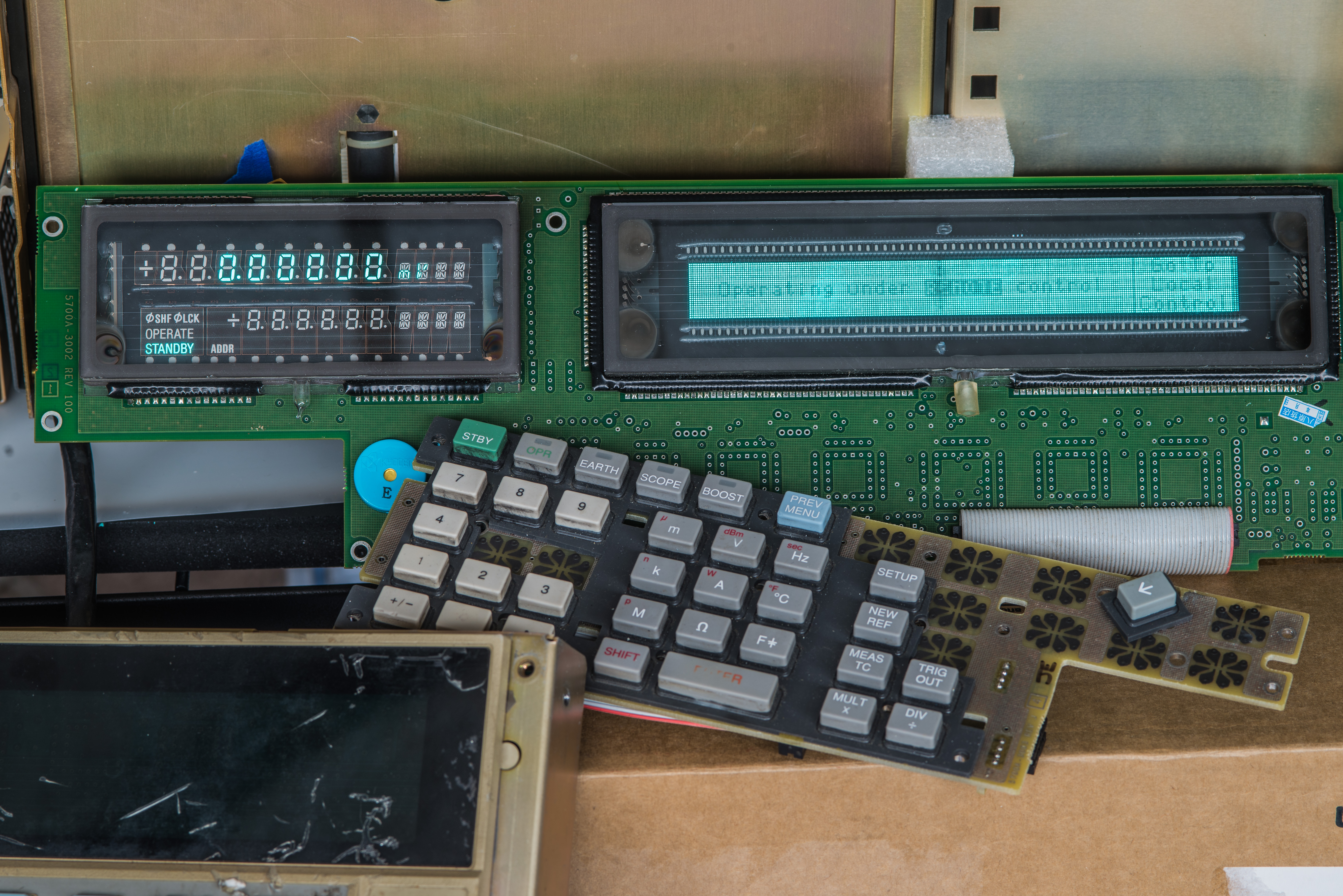
This board is good otherwise and used in another project.
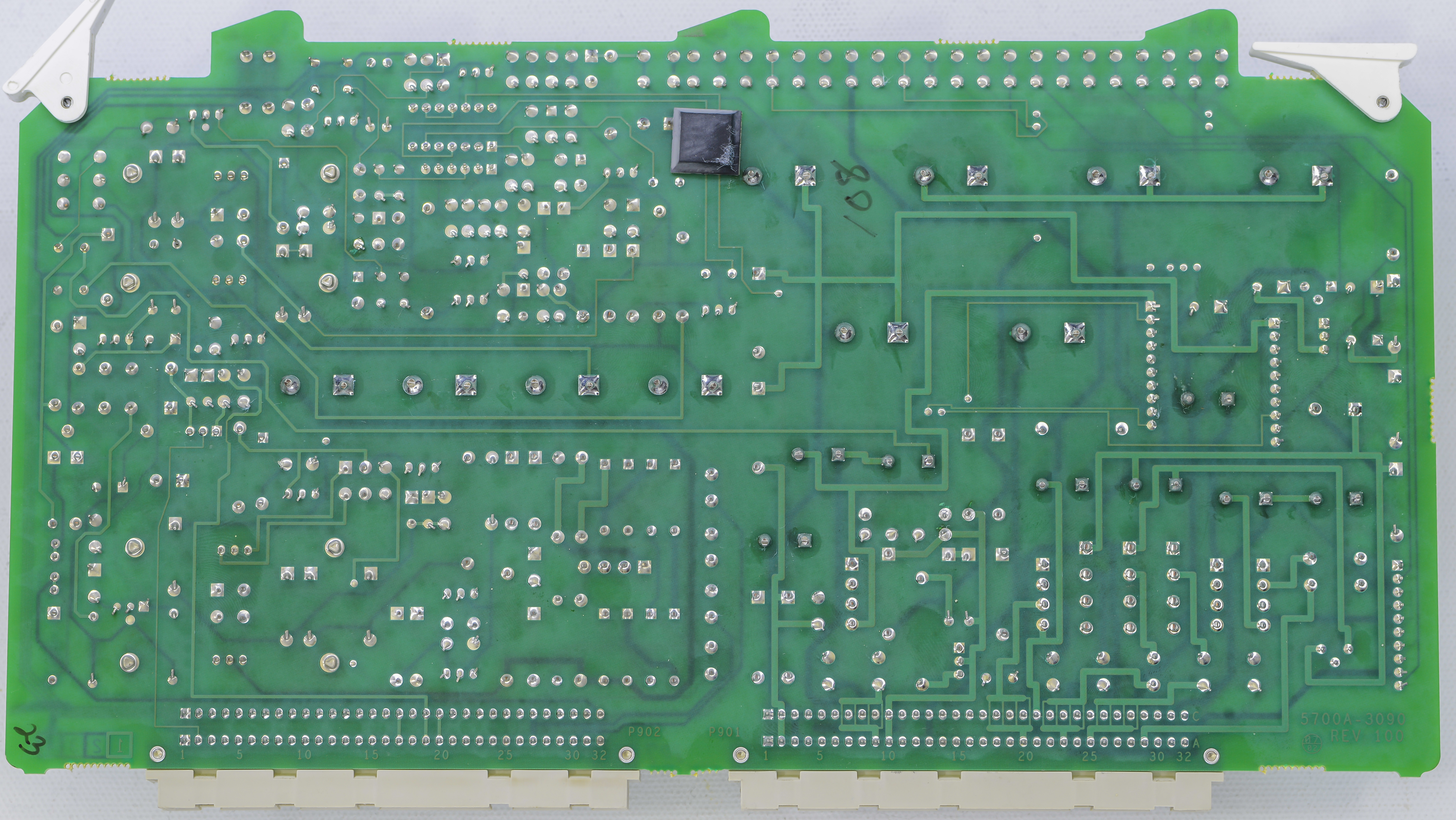
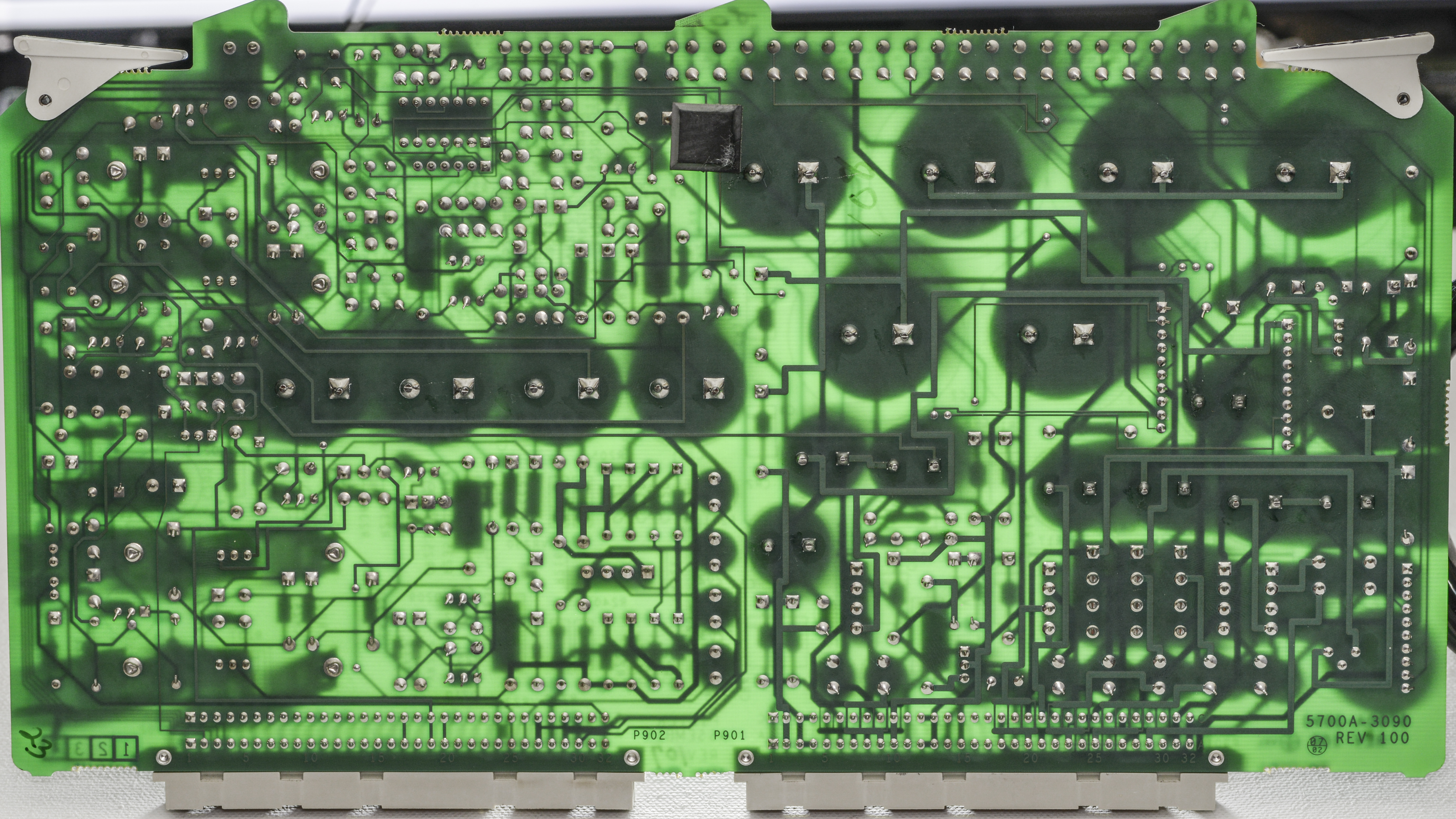
A4 outguard motherboard
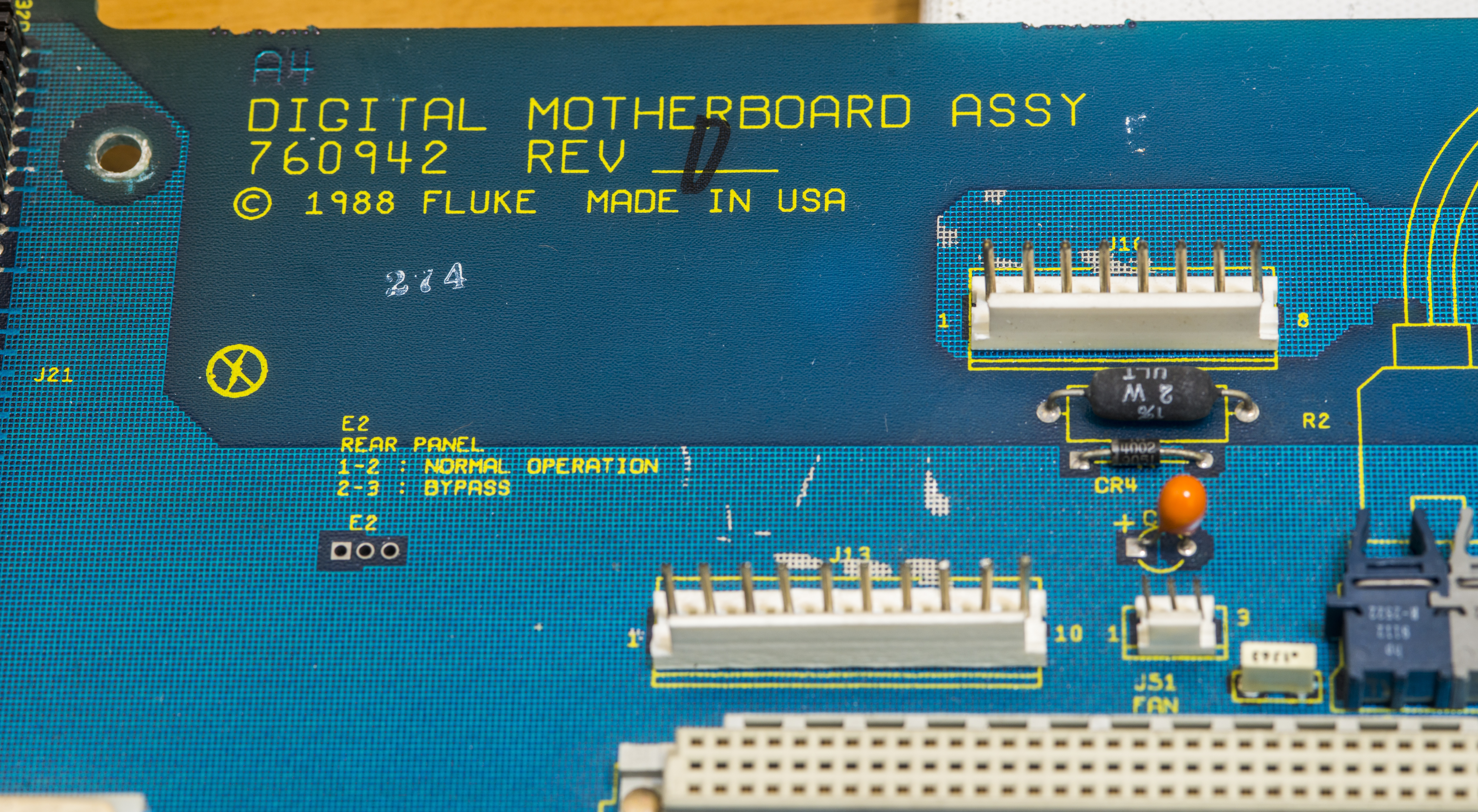
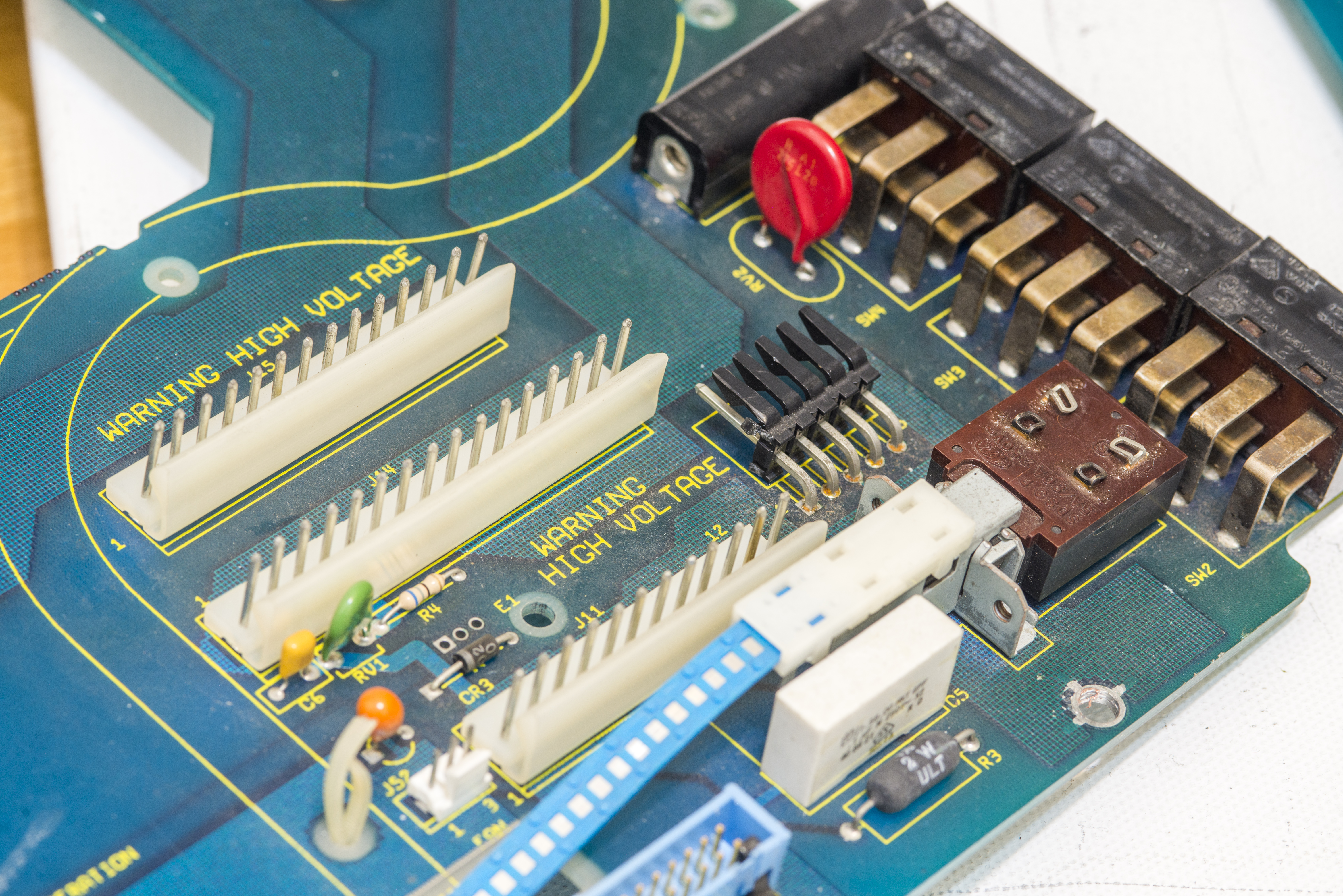

Board has internal layers damage from burn/arc flash.
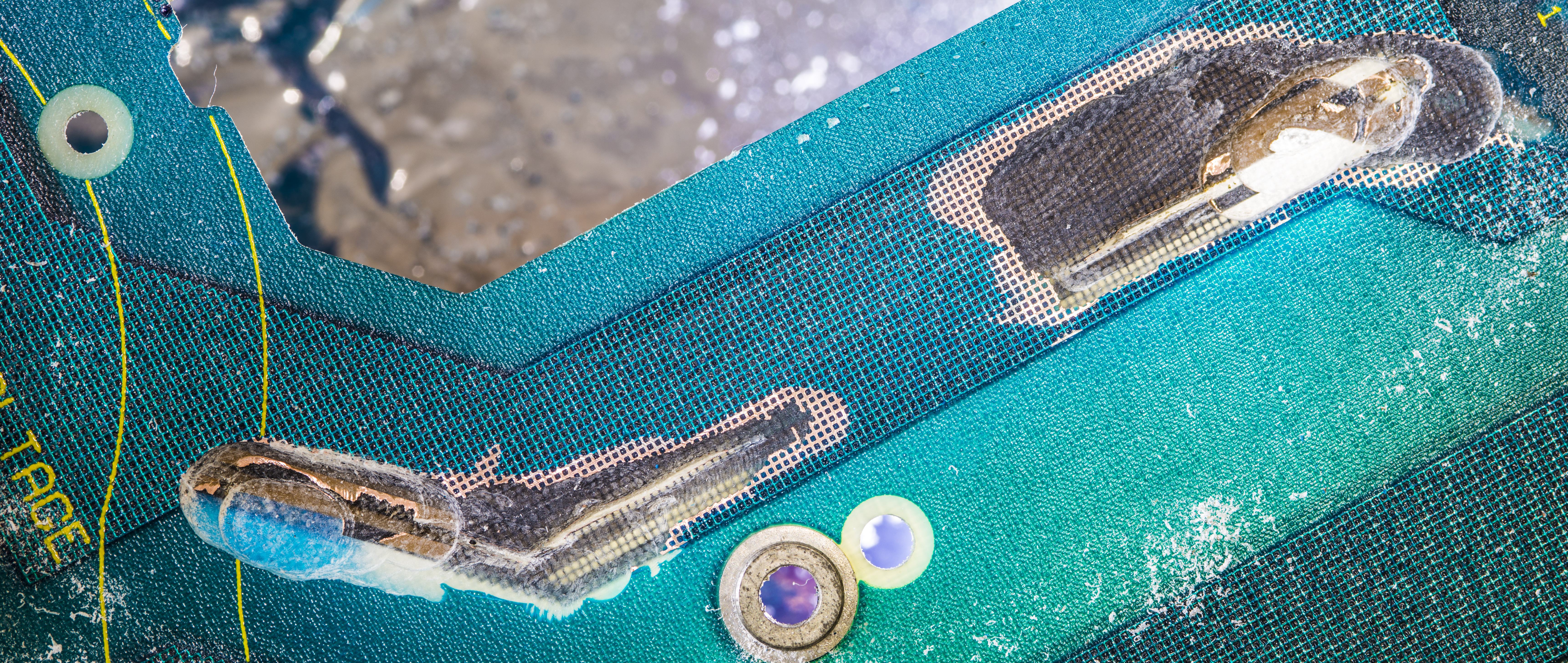
Some smashed connectors too:
Also high-voltage transformer output was shorted to +44VAC rail. So this required excavation down to layer 5, milling all carbonized epoxy FR4 material and replacing broken connections with copper straps.
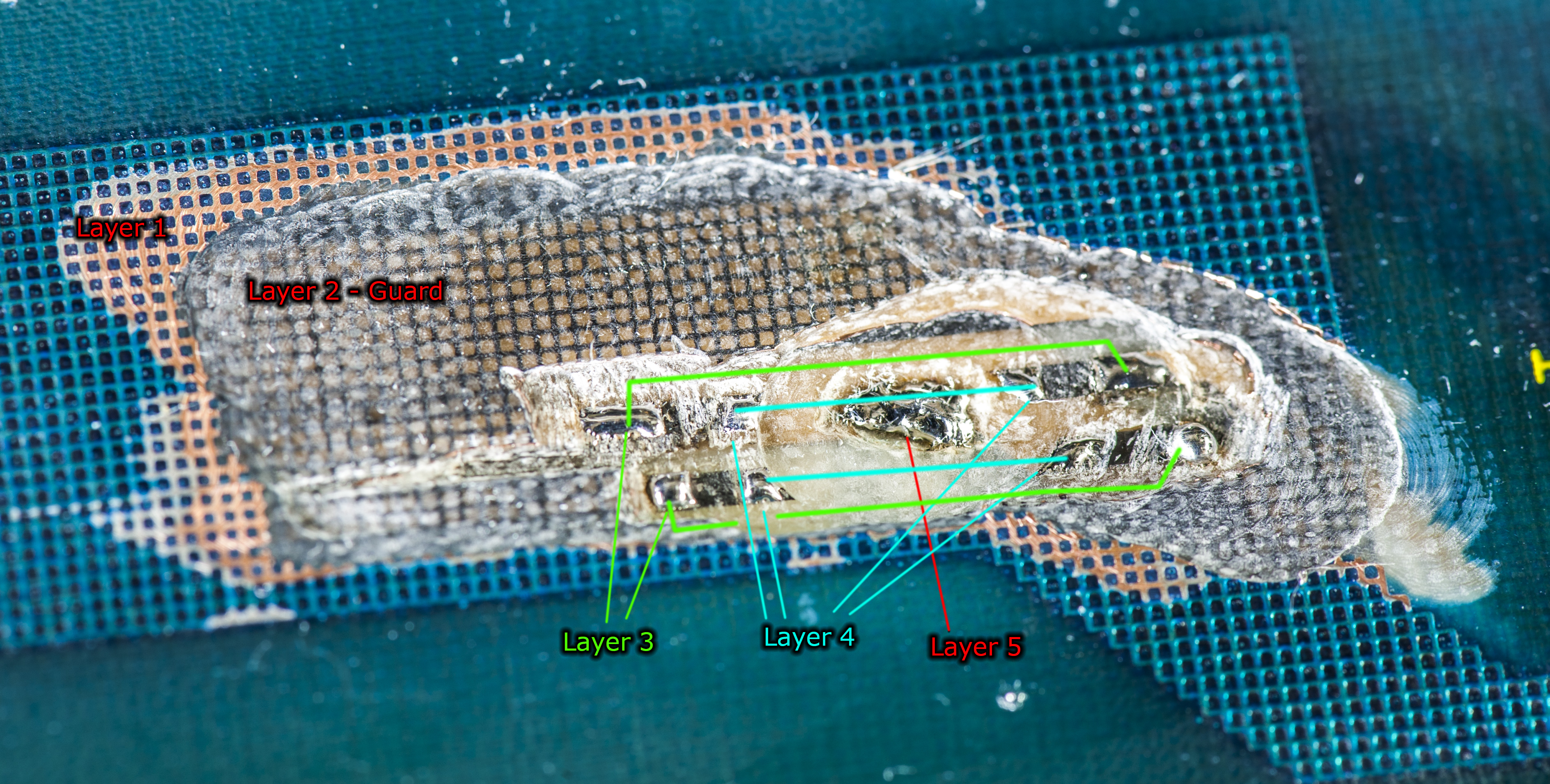
To allow spacing and insulation between “layers” additional Kapton tape was applied between connections.
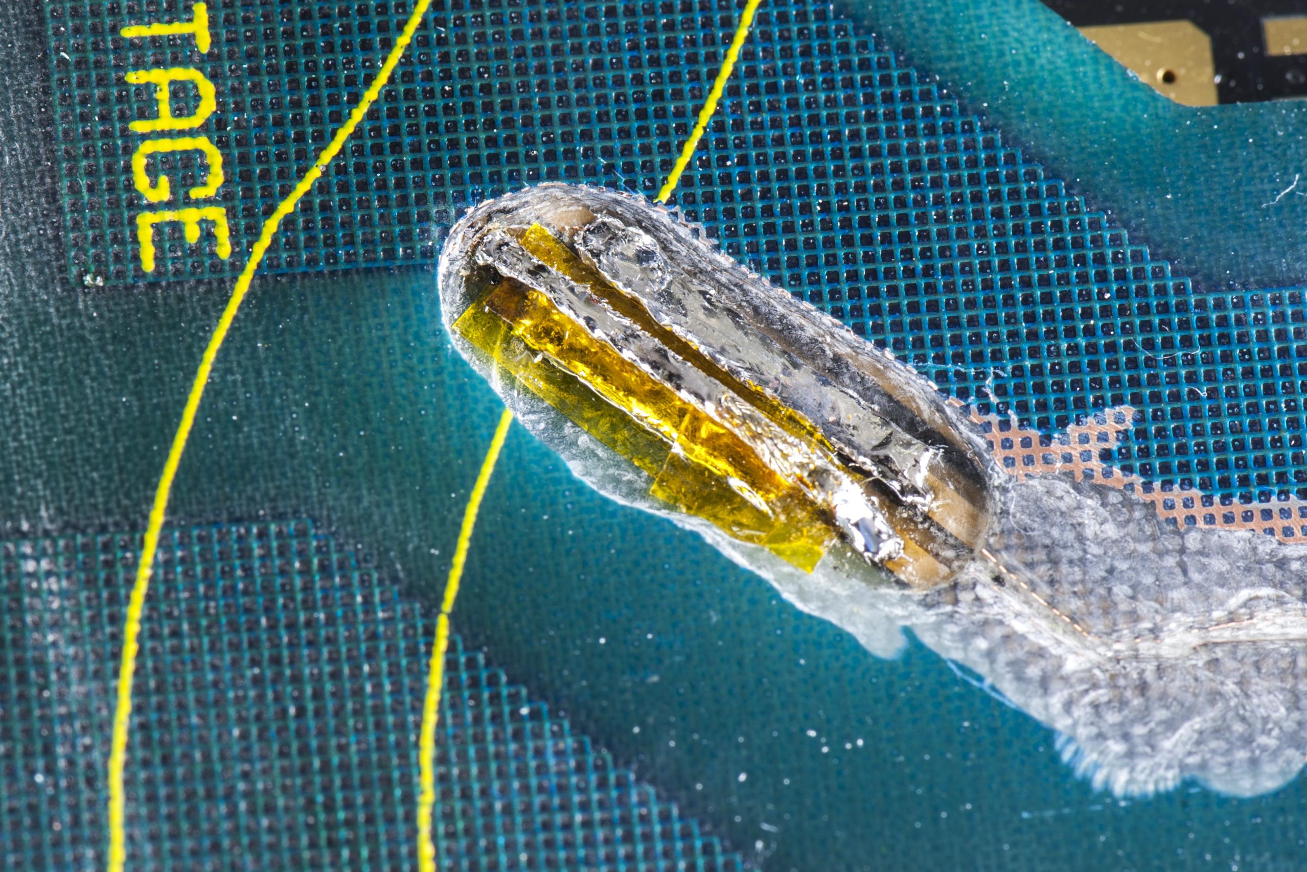
Similar process done for mains switches area.
A19 Outguard PSU PCBA
No repairs were necessary on this circuit board. For preventive maintenance all CC resistors and capacitors were replaced anyway.
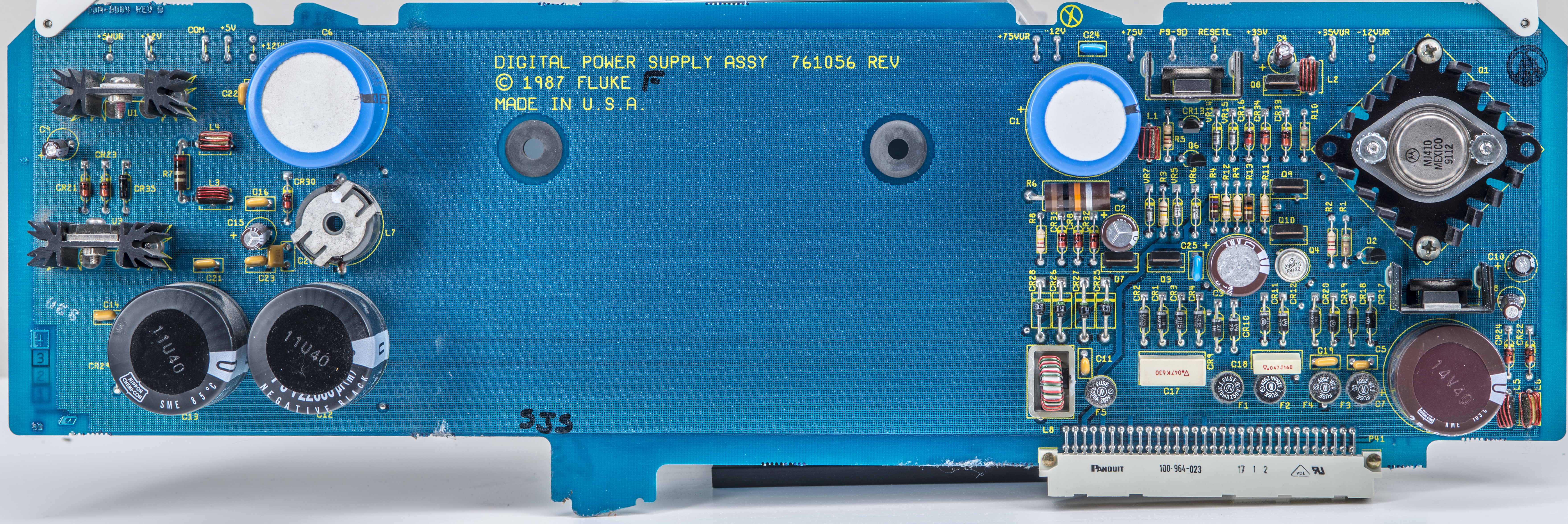
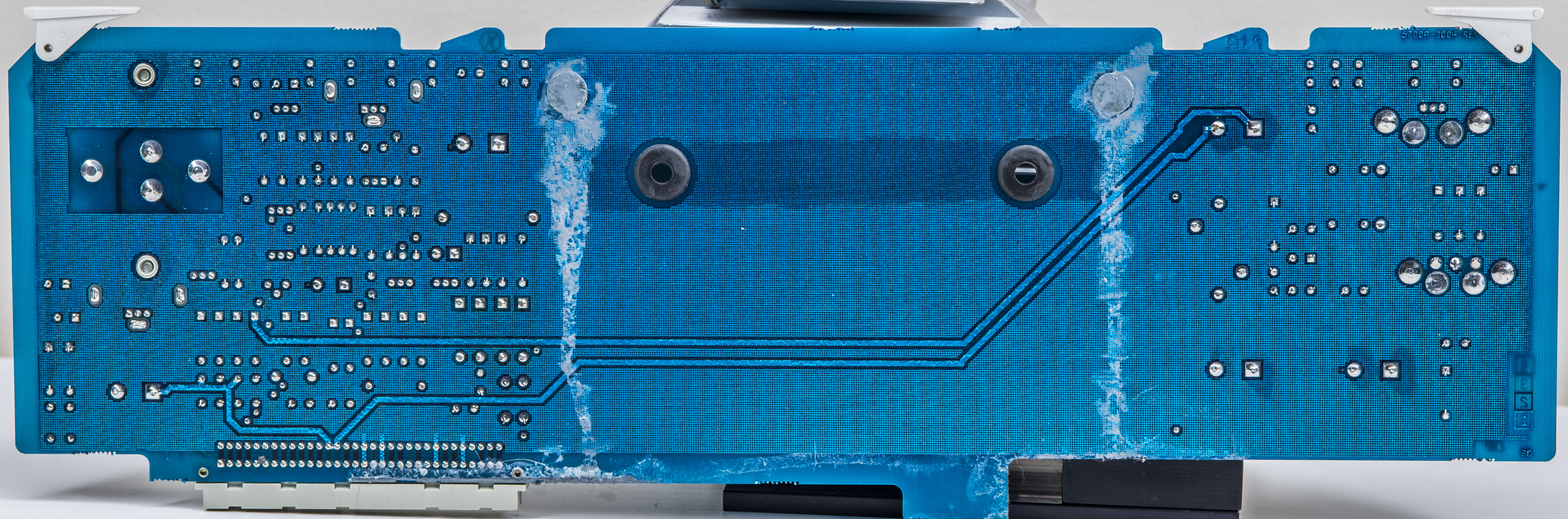
Original rubber pads desintegrated into gray goo. Typical for old 5700A boards. It was easy fix by cleaning with some IPA and replacing with brand new silicon pads. Purpose of these pads to prevent A19 touching adjacent A20 CPU board.
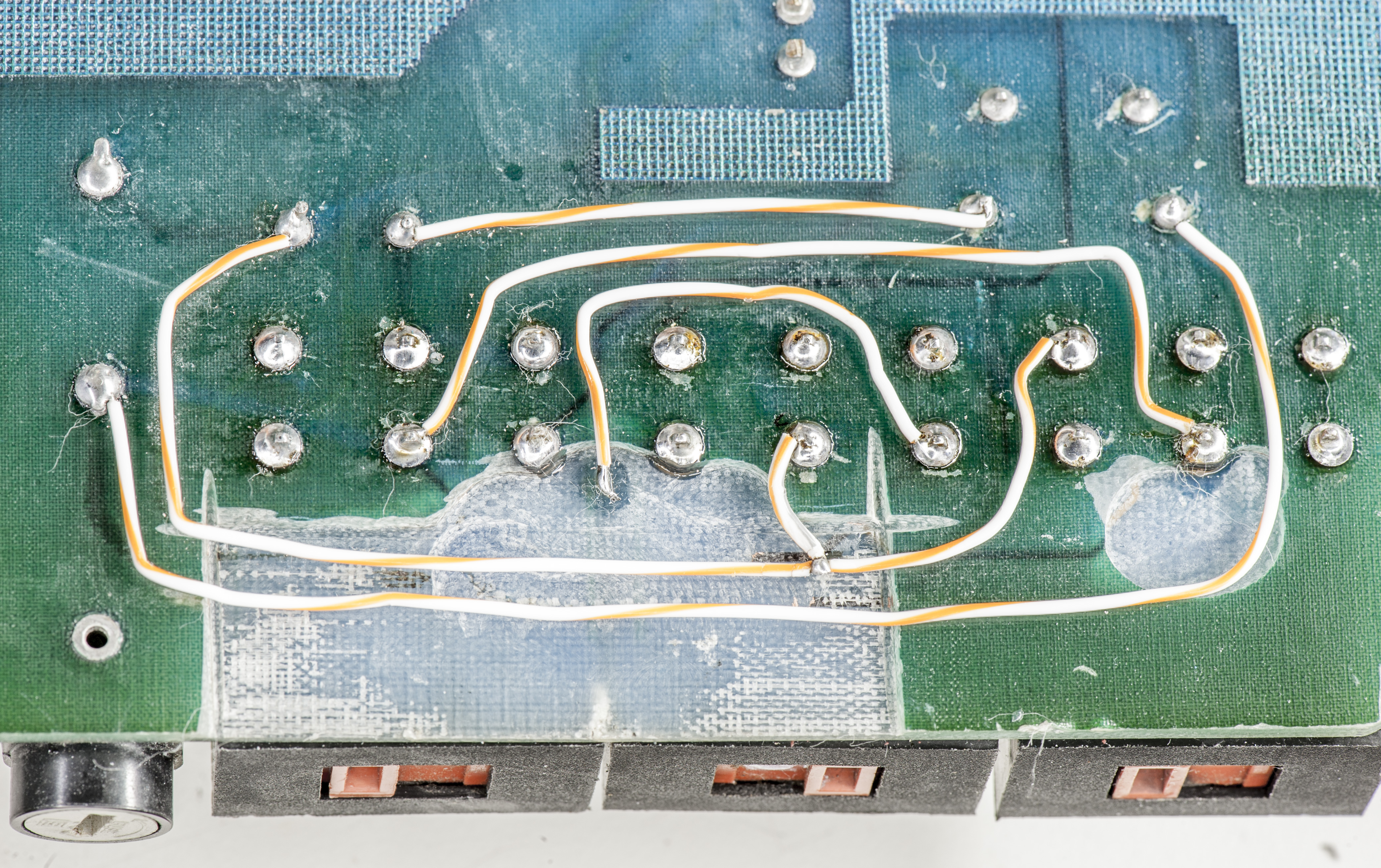
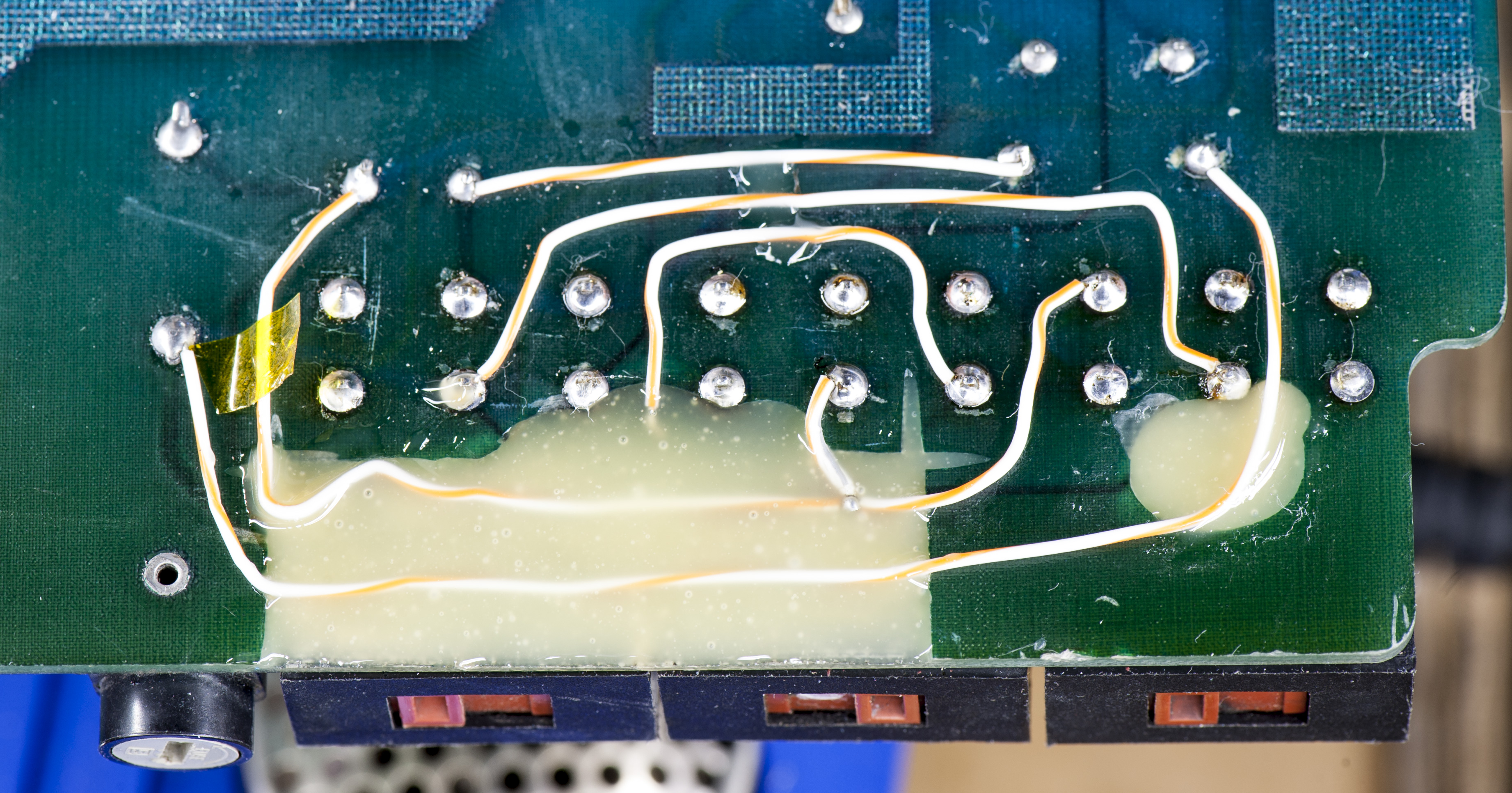
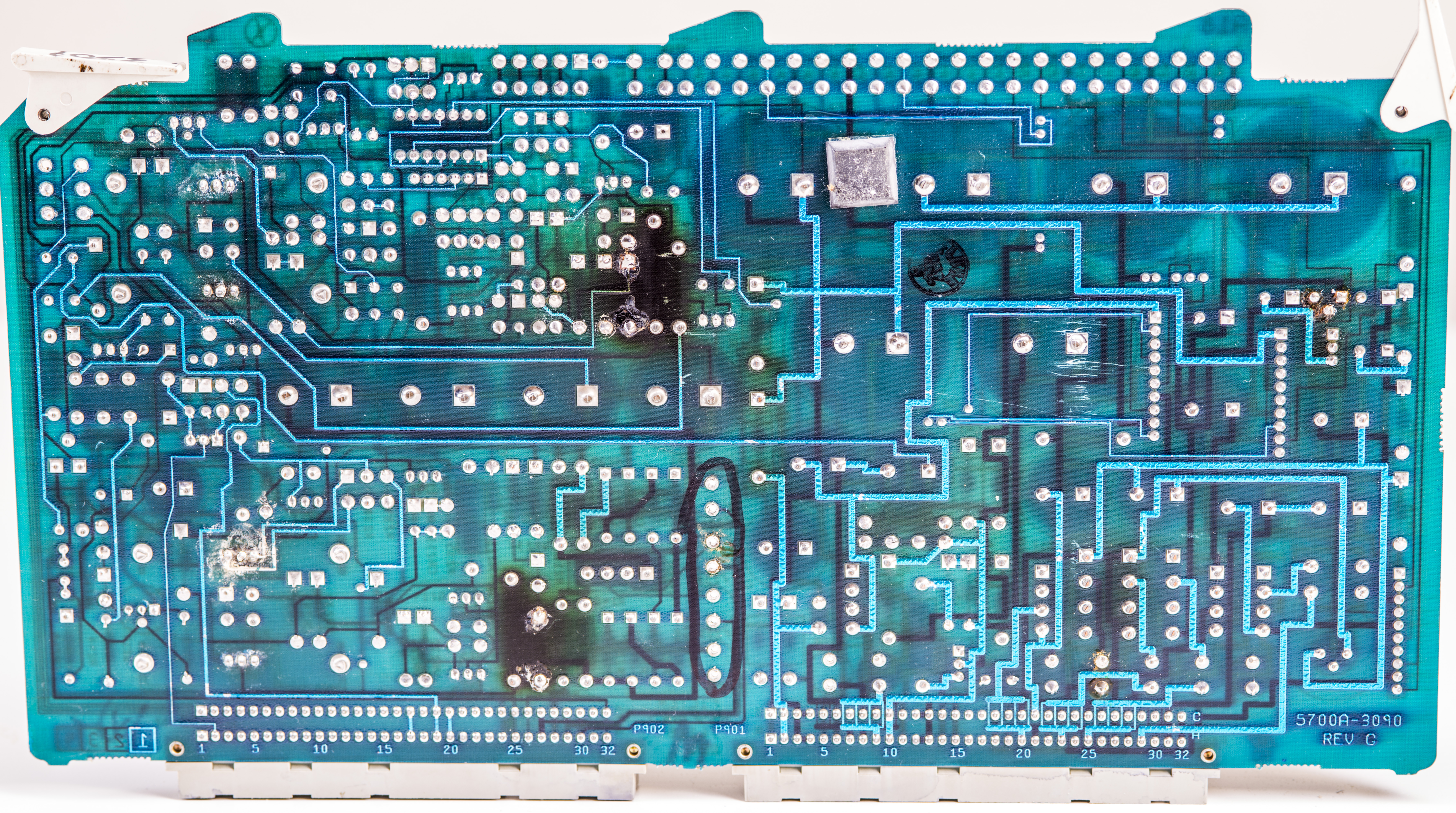
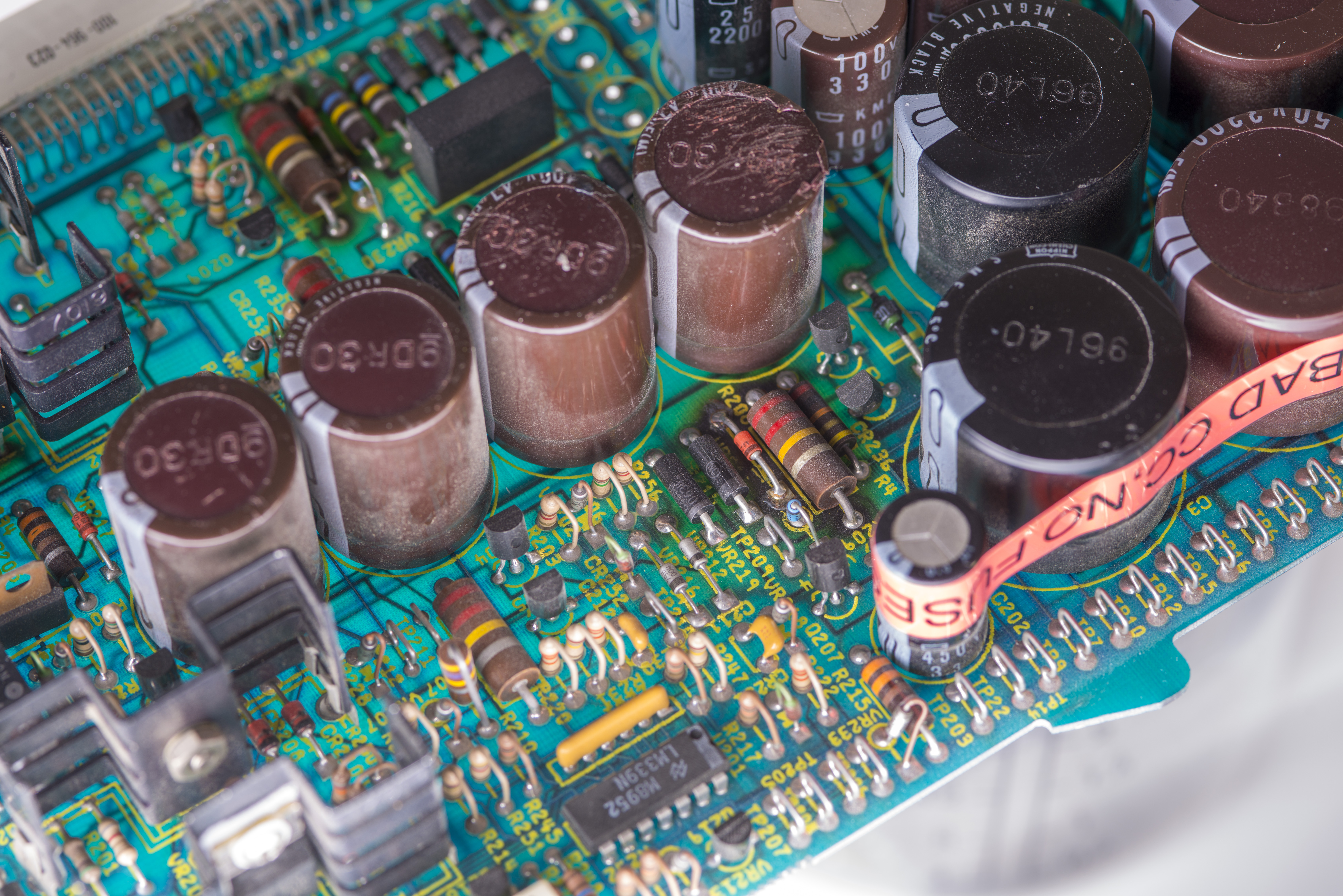
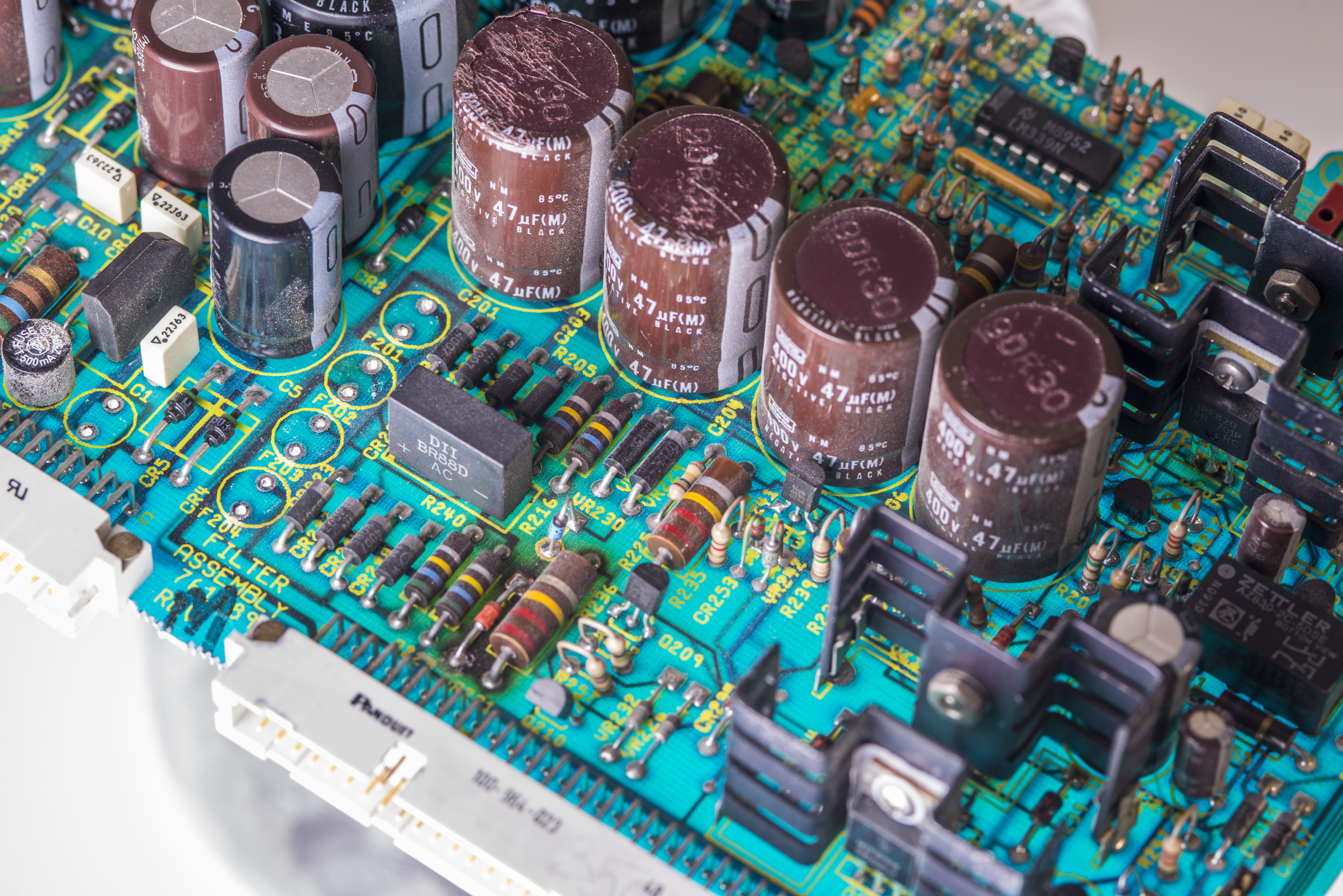
A18 inguard power supply board
This board acquired as broken with missing parts and FR4 damage. Condition as received:
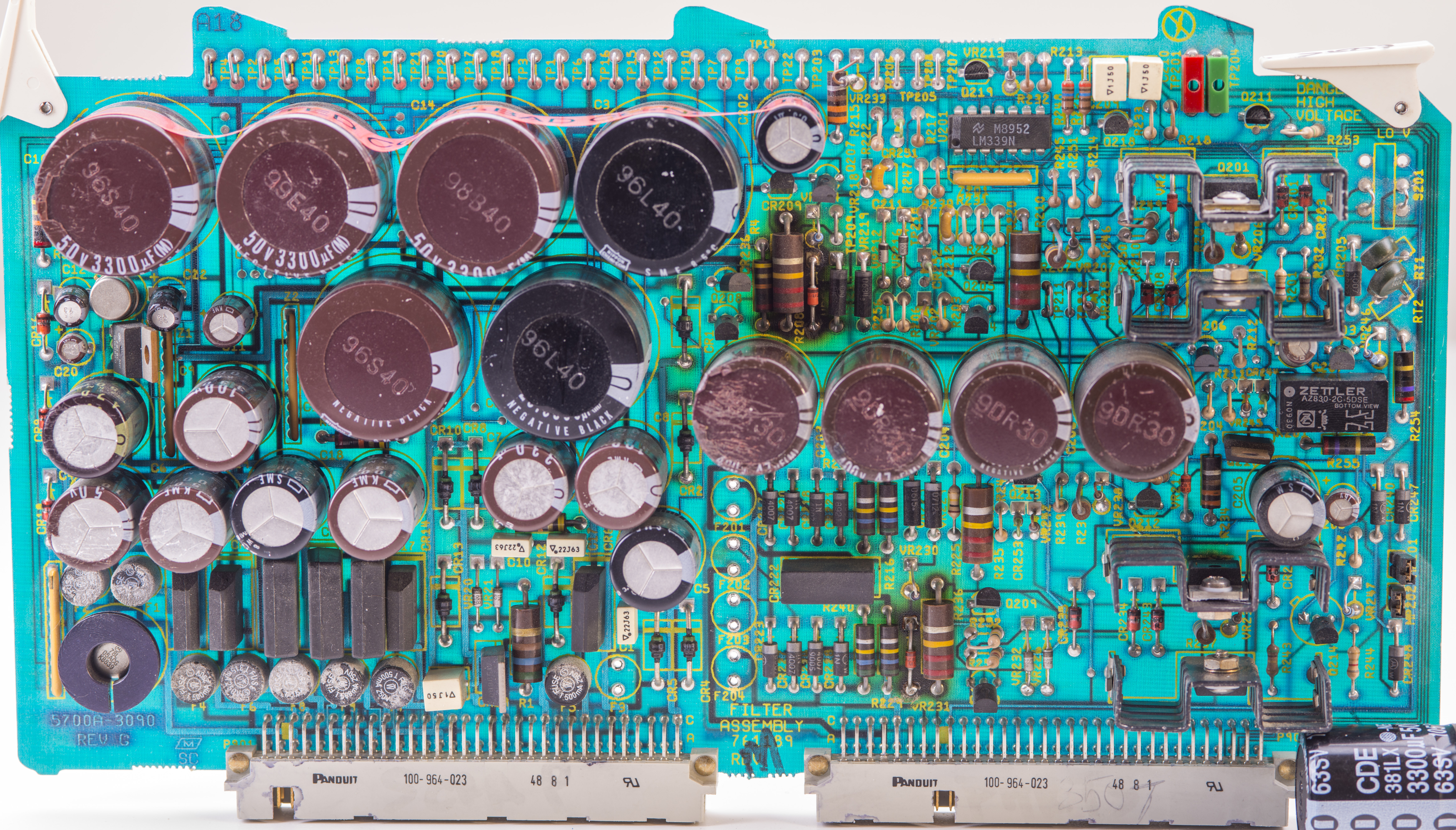
Burnt PCB around 220kΩ high power carbon composition is dead giveaway for bad board. This is very common issue for 30-year old 5700A and 5720A units. If your unit does not have burnt A18 PCB – then it’s either never been powered on for lengthy duration or have newer revision PCB where Fluke populated good metal film or PWW resistors.
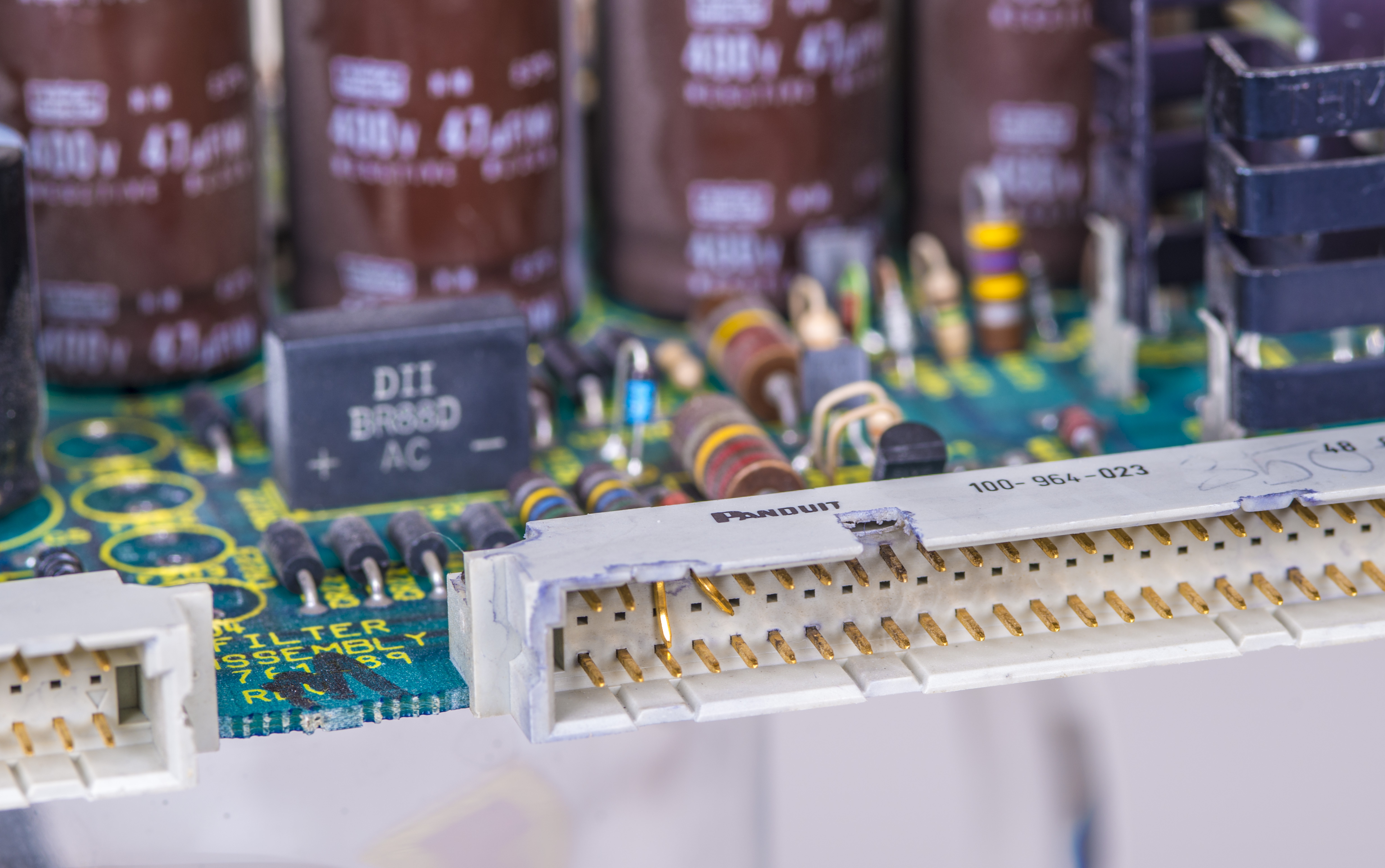
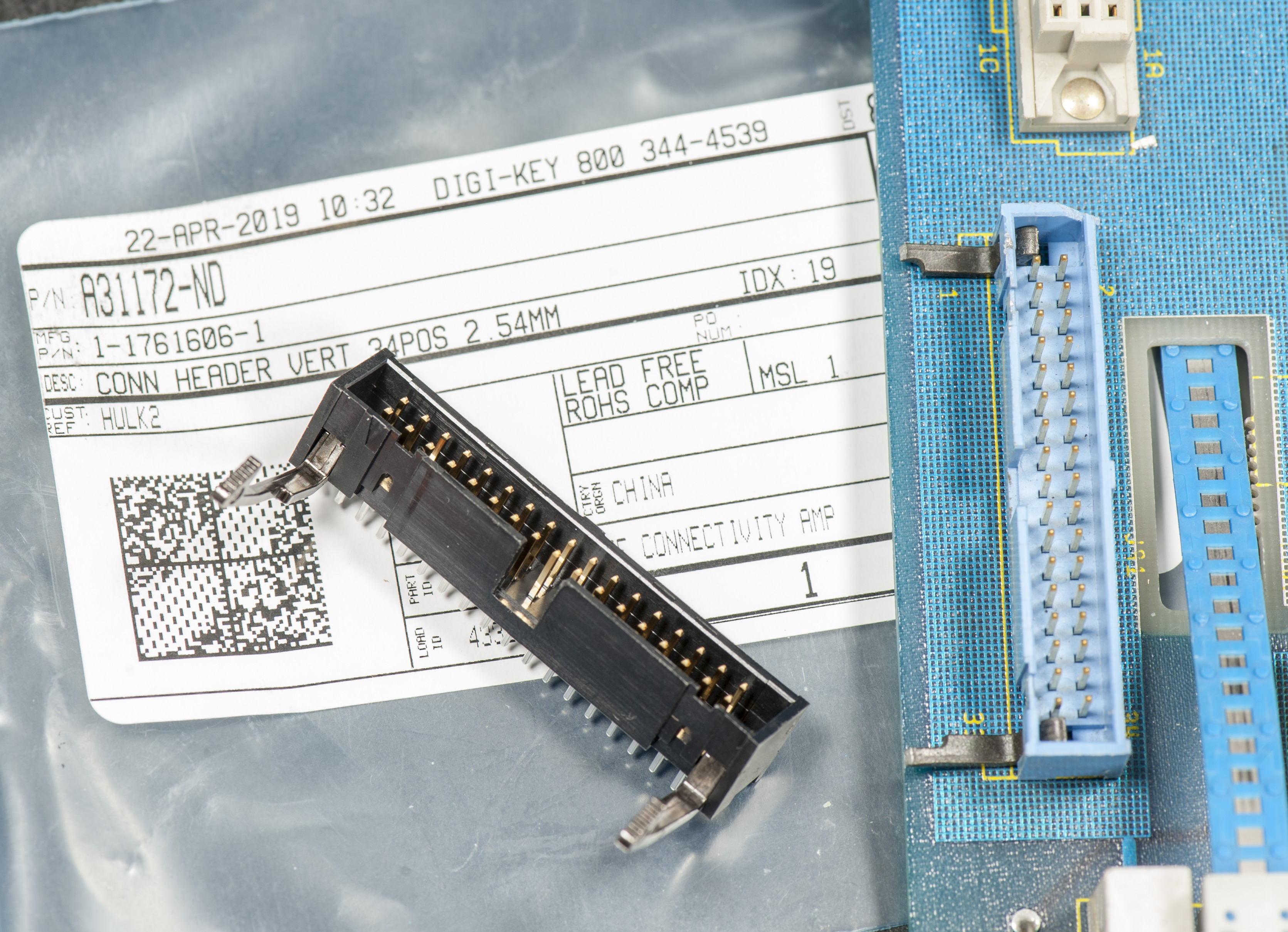
P902 DIN connector had 3 pins bent, so that had to be rectified before board would be installed in the motherboard backplane. Always check DIN connectors for bent/damaged pins to avoid further mating connector damages.
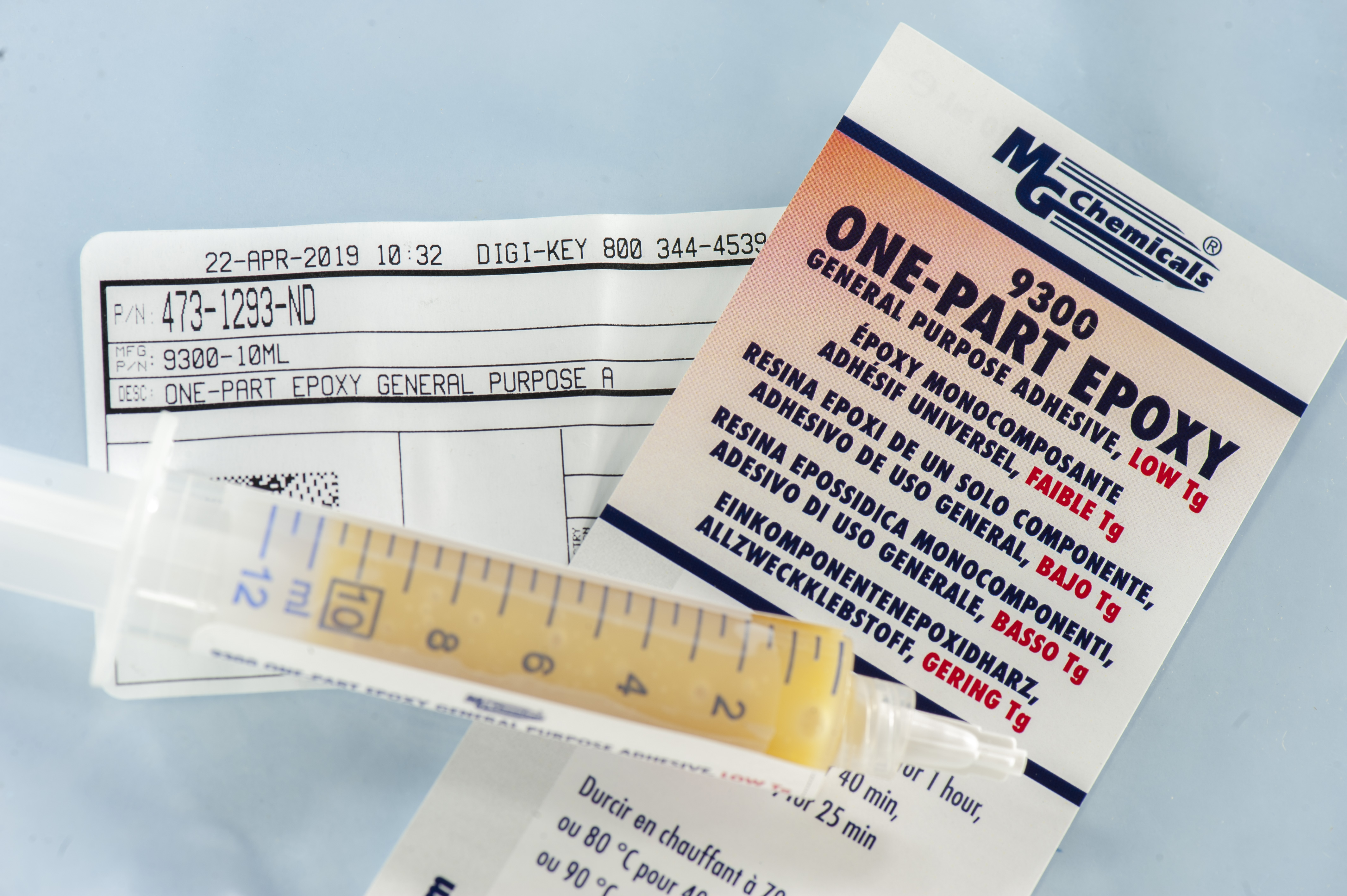
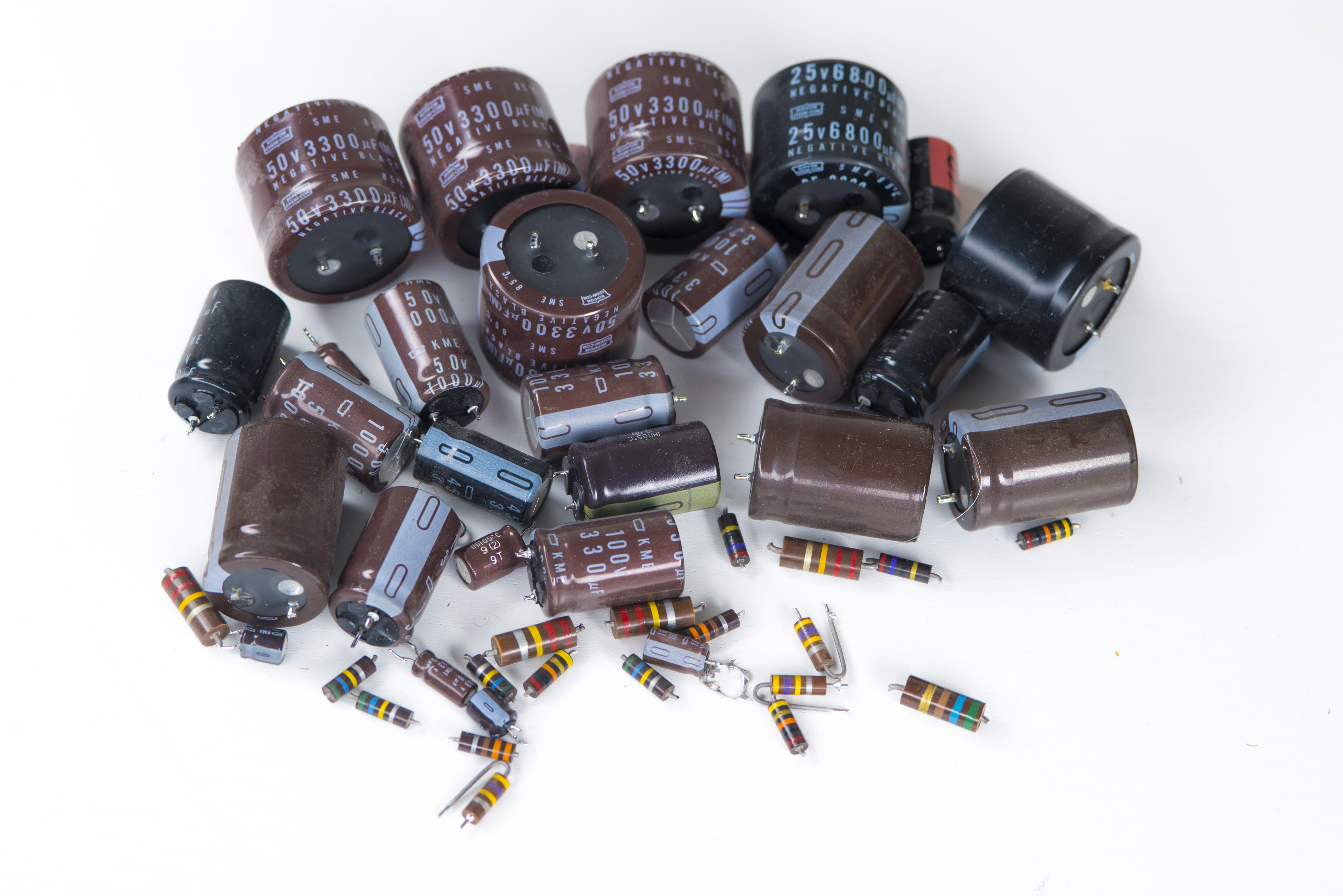
Before any troubleshooting steps begin we must replace all consumable parts, such as electrolytic capacitors (ALL!) and carbon composite power resistors that tend to fail badly with age. All replacements parts purchased from Digikey online, using BOM below.
| Part | Description | Digikey P/N | Qty | RefDes on A18 |
|---|---|---|---|---|
| cap | C16,C15,C14,C3,C202,C13,C2,C20,C21,C6,C9,C19,C18,C7,C8,C5,C4,C12,C11,C22 | |||
| cap | C201,C203,C204,C206,C202,C205 | |||
| cap | C207 | |||
| res cc | R5,R215,R207,R4,R208,R239,R210,R207,R238,R225,R229,R205,R216,R240,R224,R236,R235,R237,R209,R254,R255,R234,R2,R3,R1 | |||
| fuse | F3,R204,R203,R202,R201 | |||
| diode | VR211, VR215, VR219, VR210, VR231 |
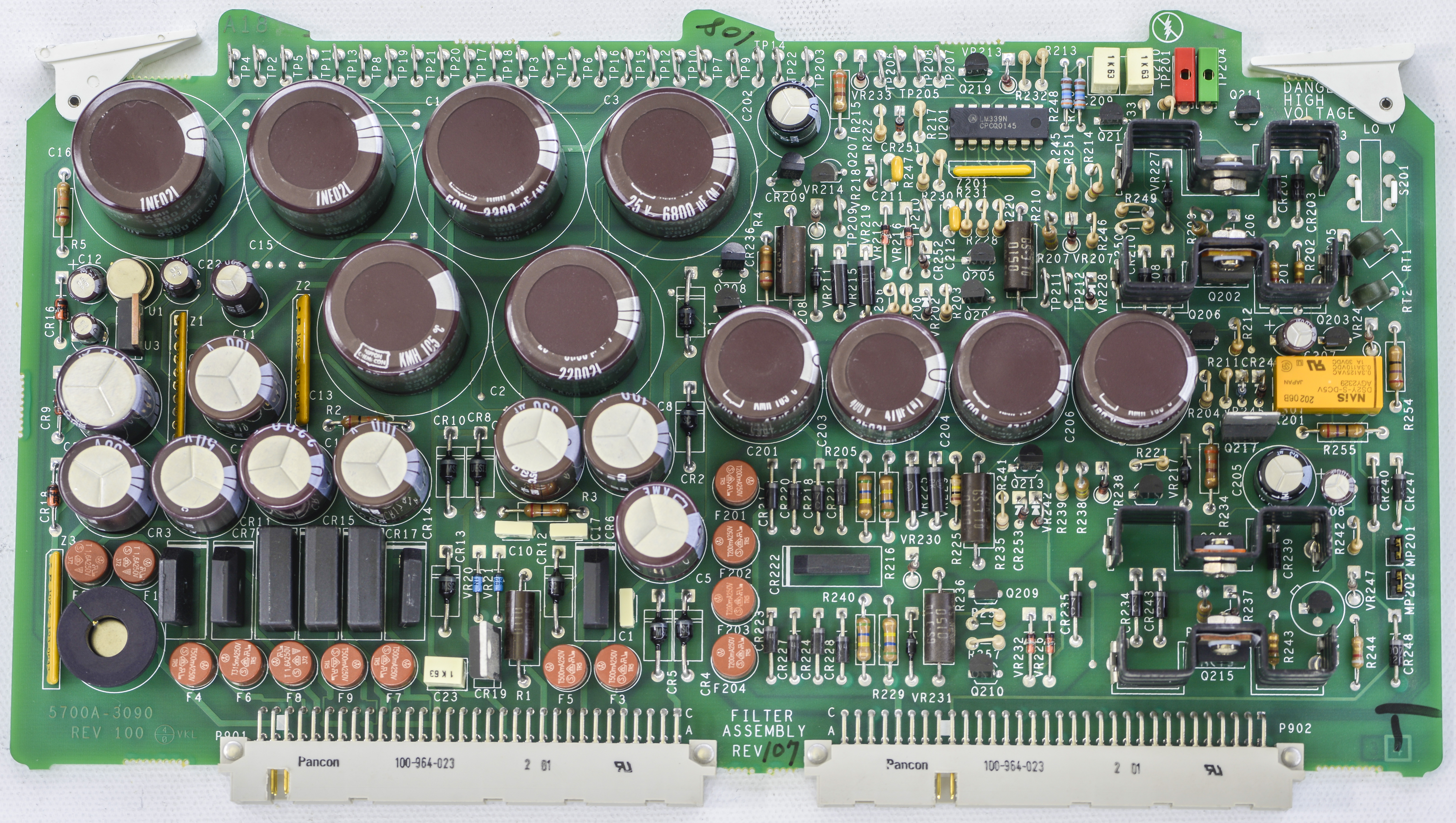
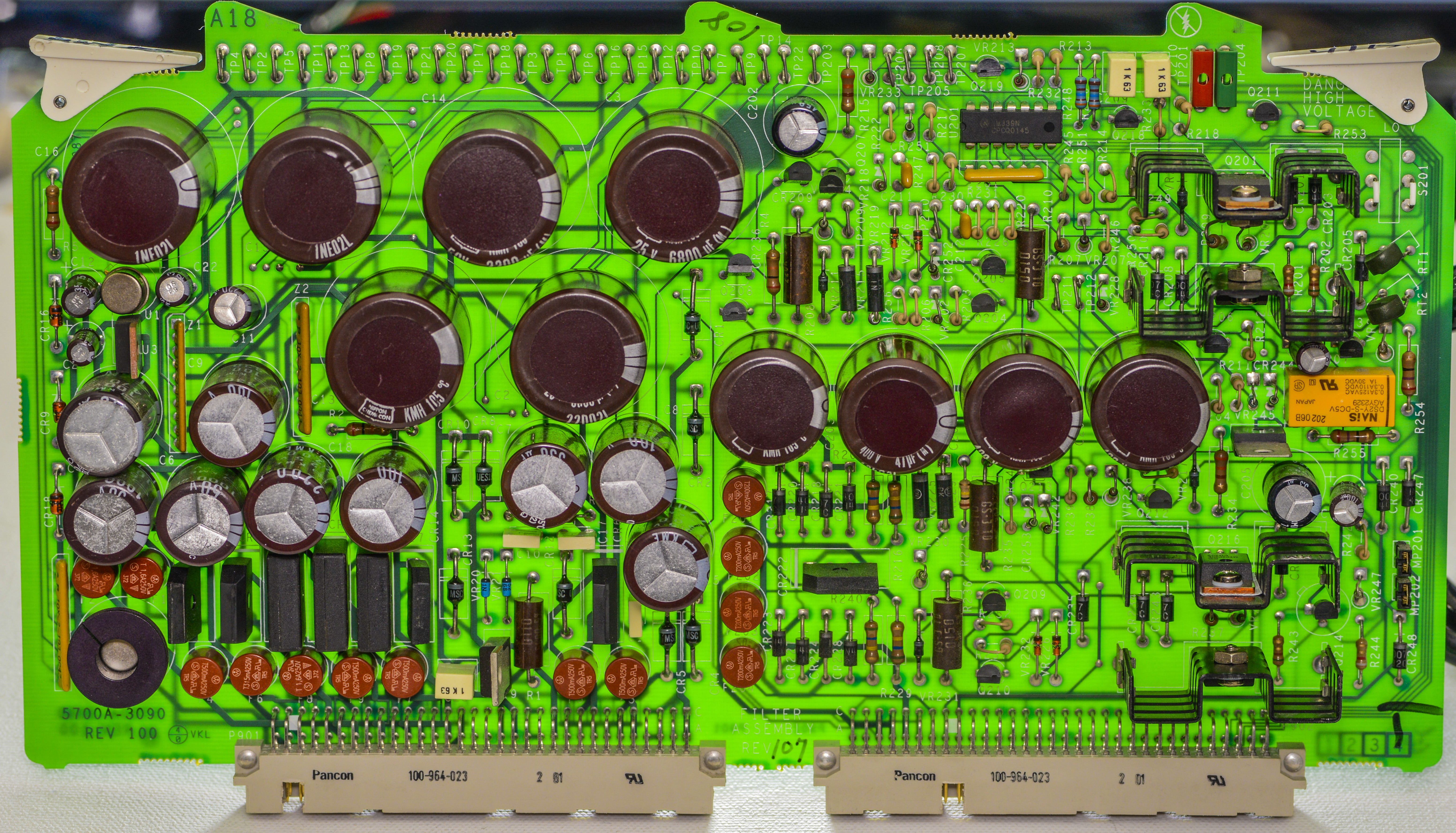
Here is for comparison how modern 5720A latest revision A18 board should look like:
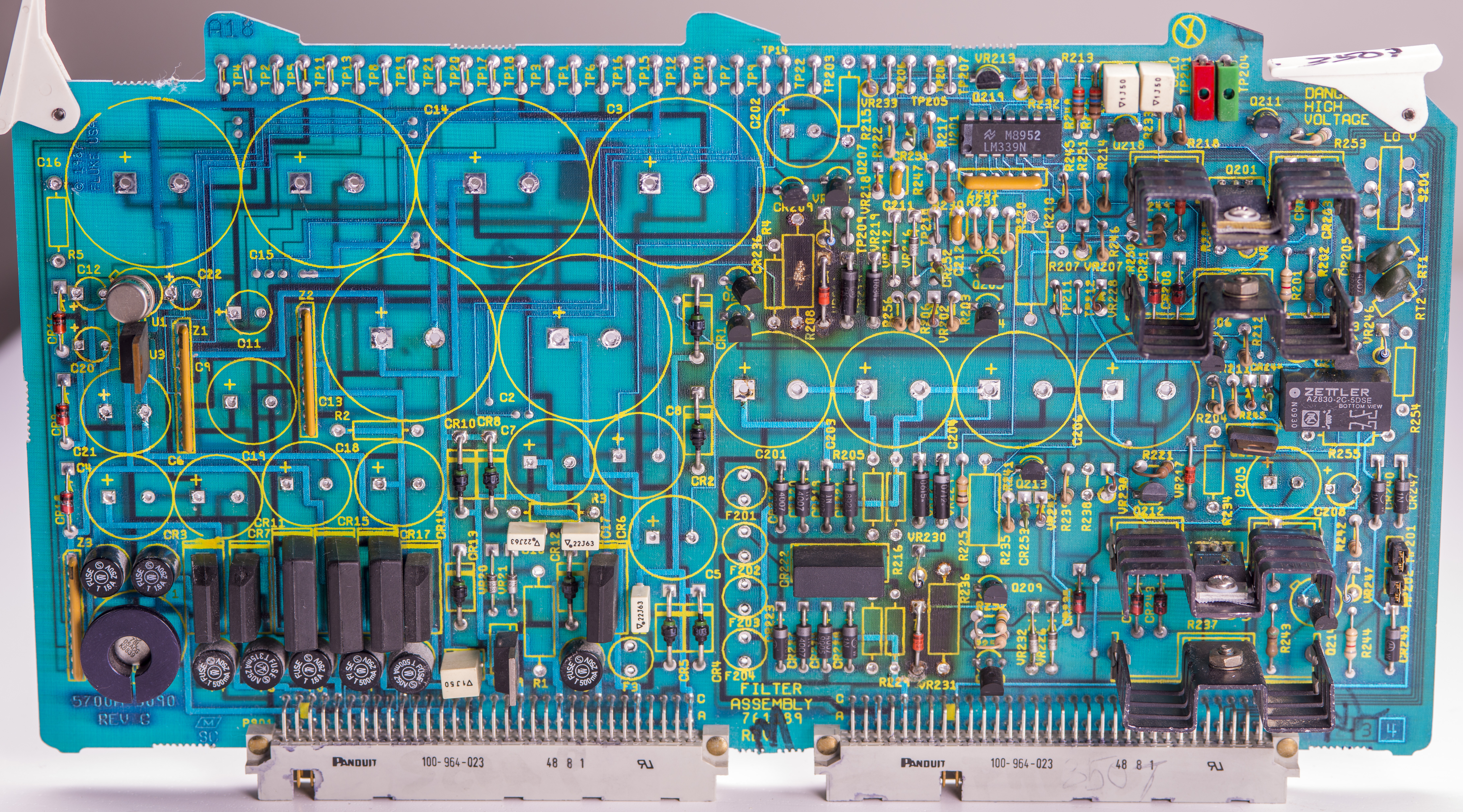
After sniping all bad parts out we got quite a pile already.
After replacing all CC resistors and electrolytic capacitors board was installed in calibrator and powered on. All low voltage DC rails checked out okay. Not so lucky with high-voltage section supply. Without smoke or sparks input 200mA fuses F202 and F203 were blown open. So this part will need more troubleshooting.
A17 Inguard regulator power supply and inguard crossing
This board received as broken/unknown condition with missing metal shield/airflow duct cover.
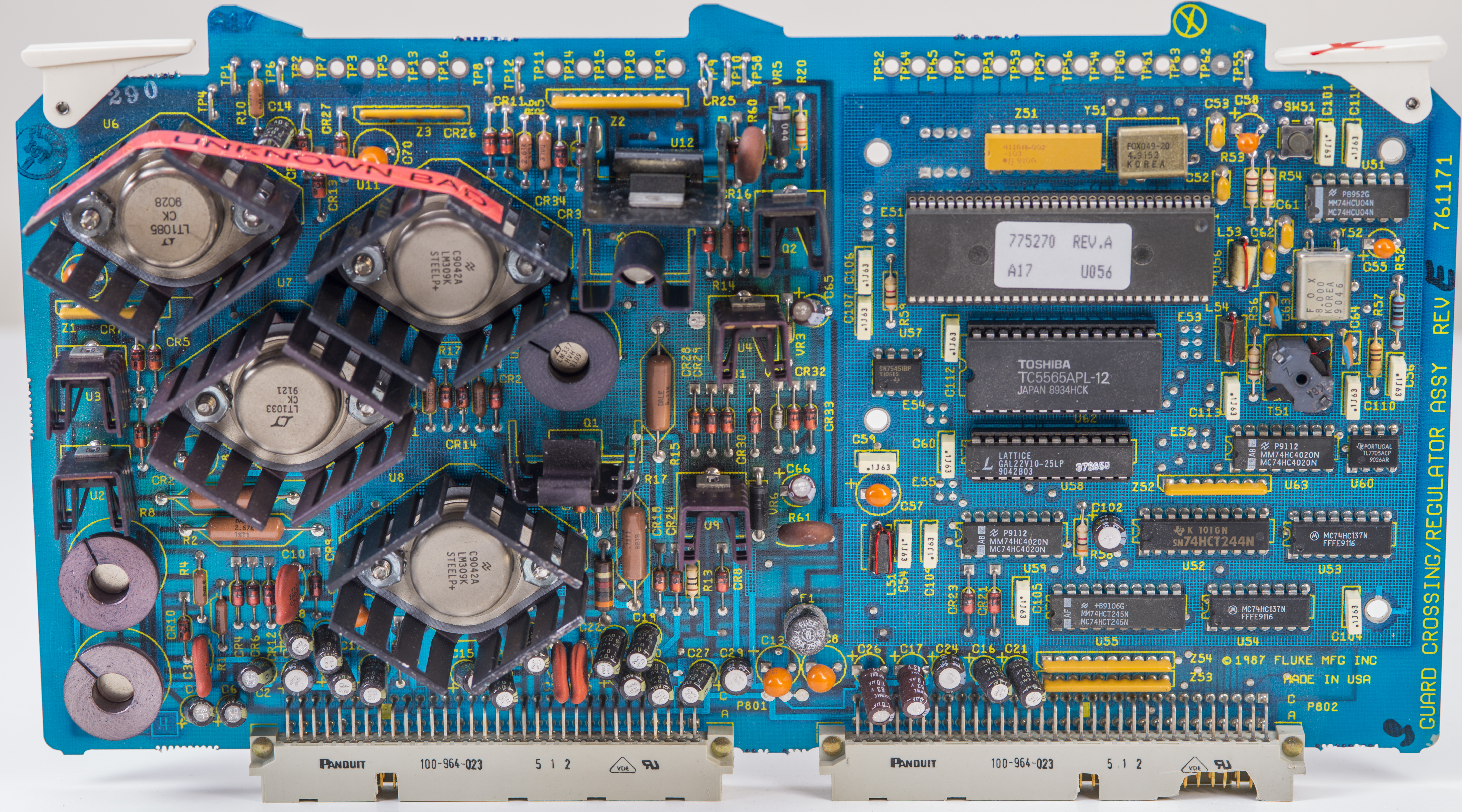
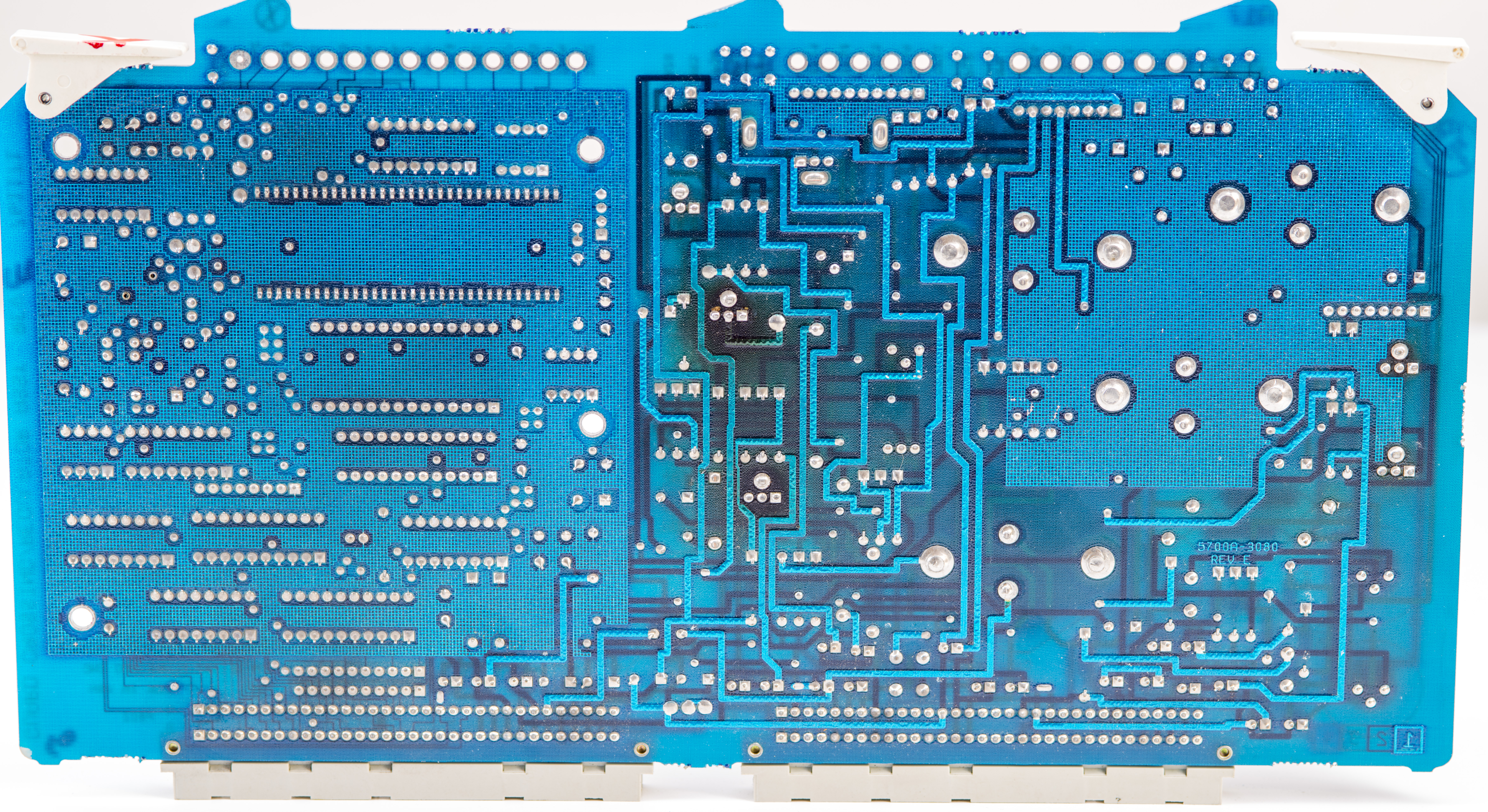
TBD
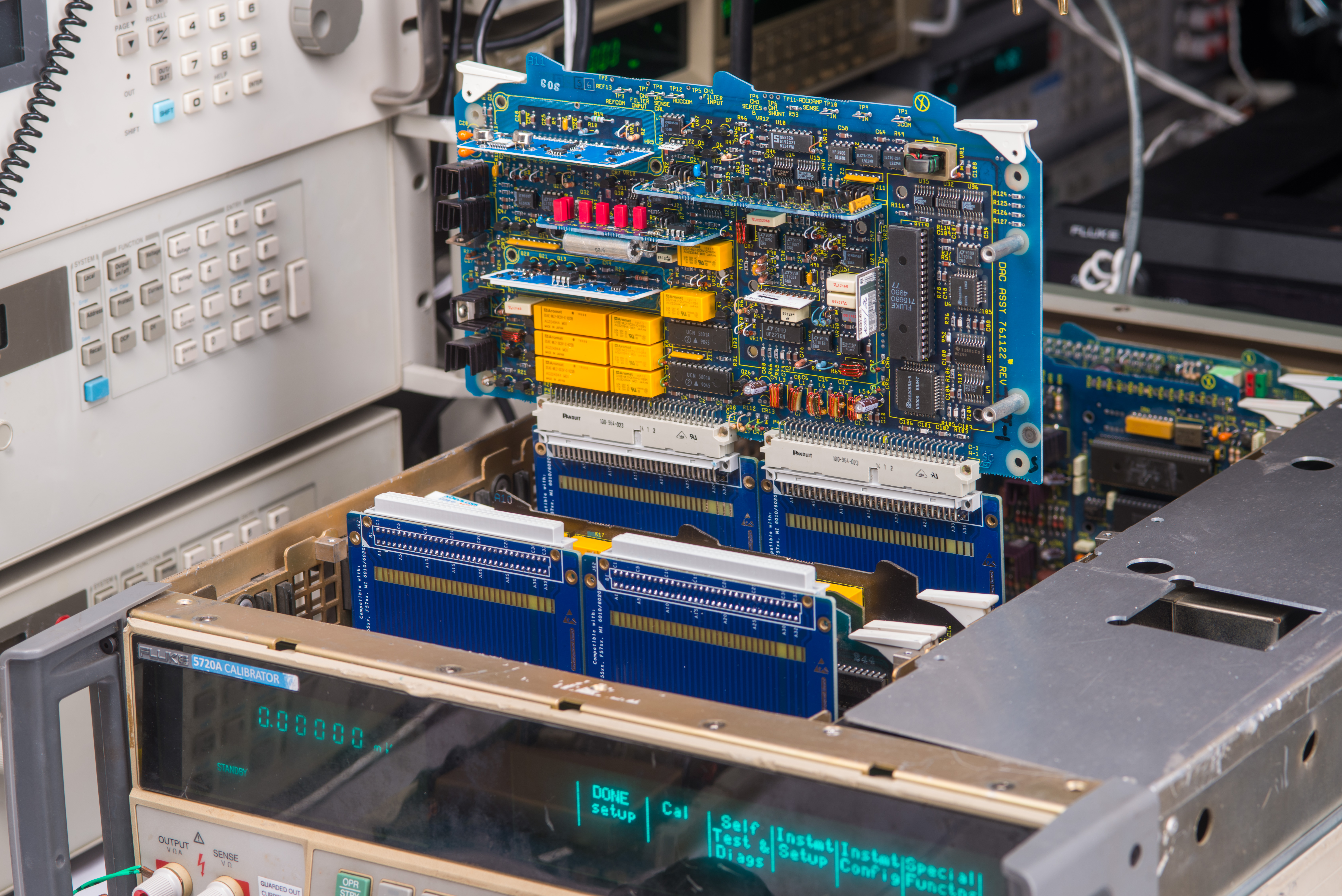
First outguard power on test
For this test 110VAC supplied from Chroma 61604 AC source to calibrator. Calibrator is populated with A1,A2,A3,A4,A19,A20,A21 boards only. None of the inguard analog PCBAs installed.

Yay, it’s first power on for Hulk-3 5700A project! During this test calibrator consumed ~24W (without fans). Now we can proceed with next step, fixing most important A11 REFDAC. All calibrator functions depend on operation and performance of A11 assembly.
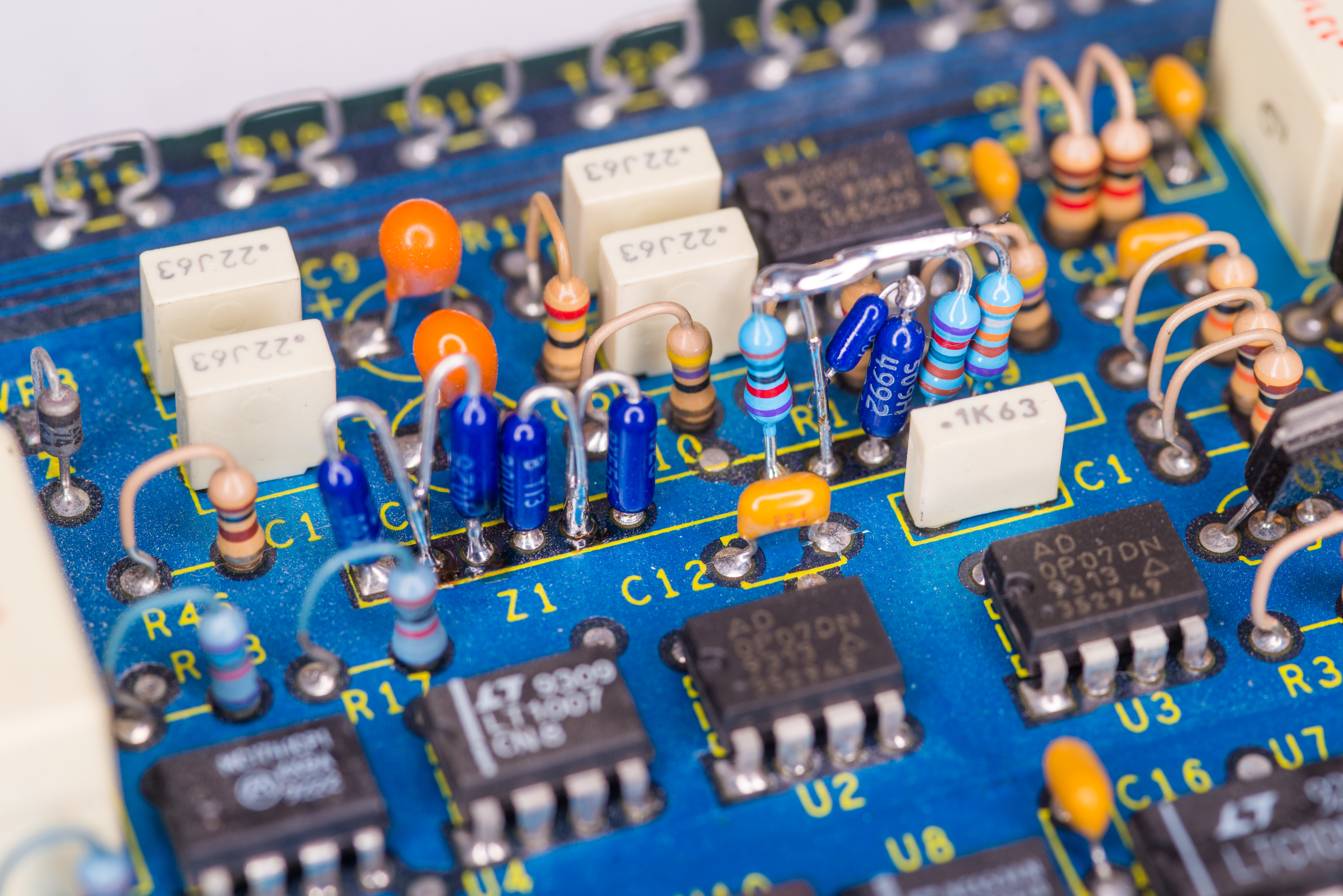
A11 reference/DAC board
A11 reference/DAC board, second board
Second A11 board came while ago with some random listing on ePay, included with some other 5700A parts. With this board installed in the calibrator self-diagnostics reported lot of A11-related problems, such as:
- 13V Reference fault
- 6.5V Reference fault
- A11 monitoring fault
- +11V DC range failure
- -11V DC range failure
- +22V DC range failure
- -22V DC range failure
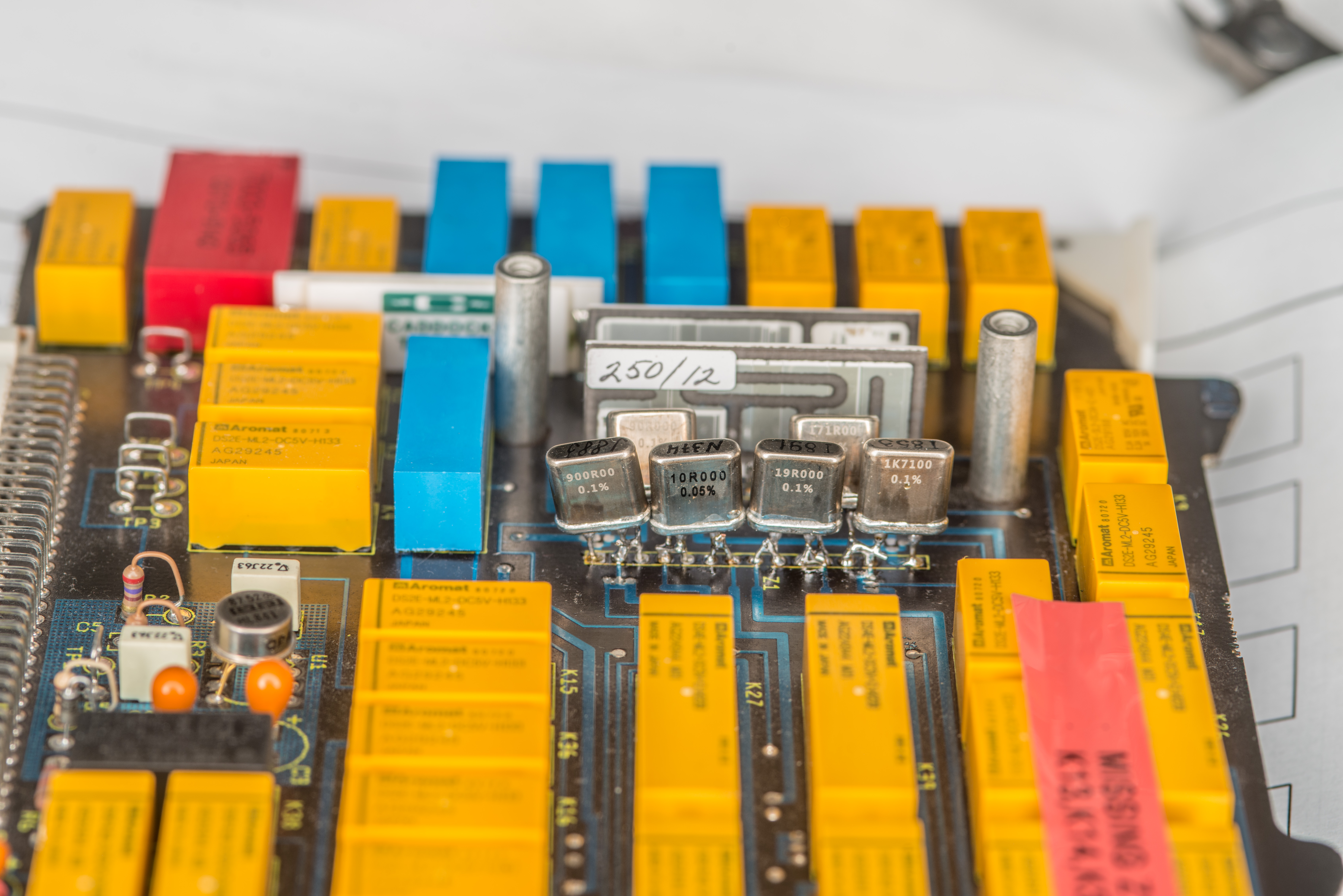
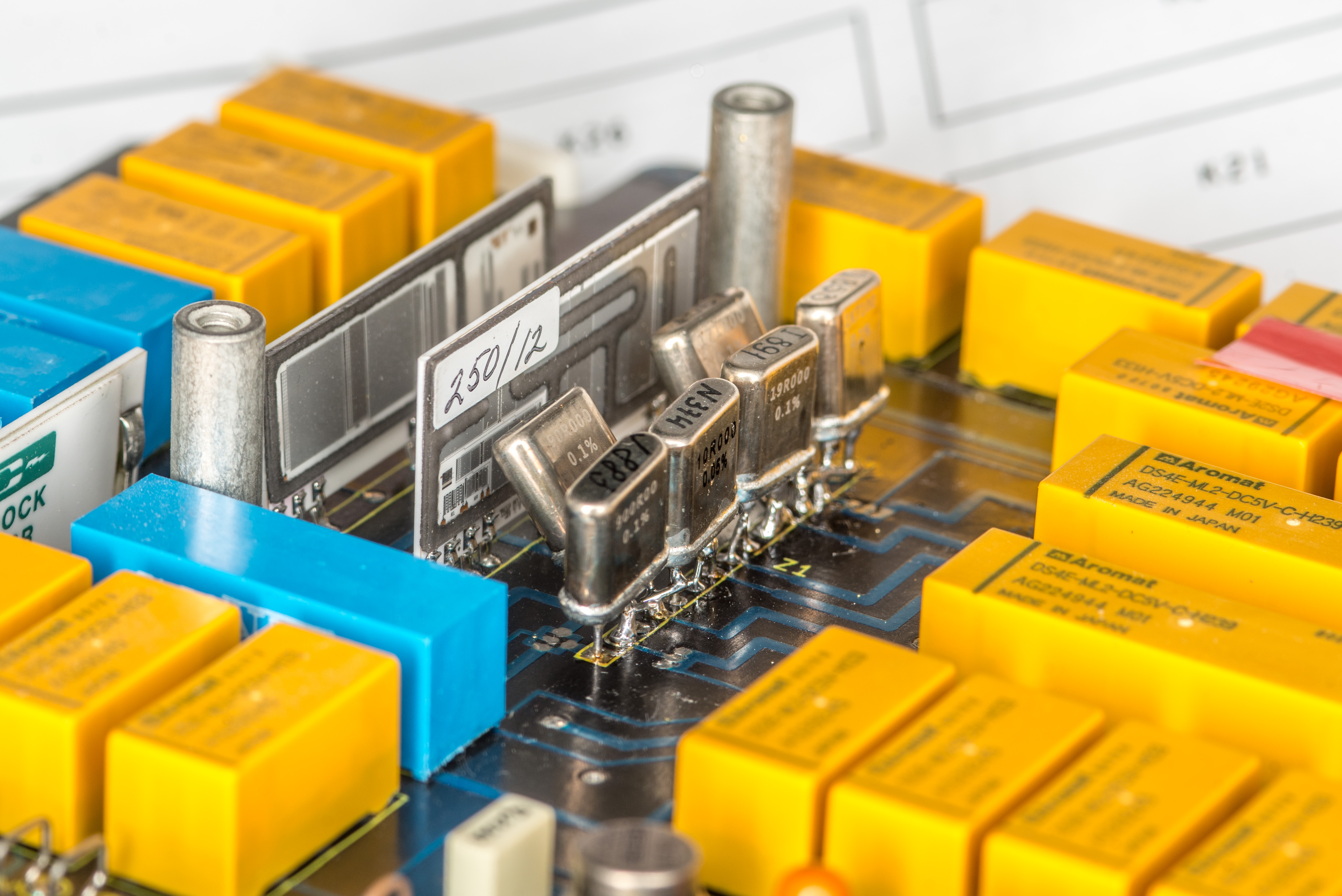
And many more. Something is very broken on this assembly. Let’s take some thermal images and investigate if there is something cooking out of ordinary. A11 has two oven hybrid assemblies – reference module and output buffer amplifier. Both hybrids have matching precision network attached with harden epoxy to alumina plate and embedded heater. Both hybrids covered with plastic cap to protect from airflow and maintain isothermal environment. Buffer amplifier regulated at +52 °C while reference assembly maintained at +60 °C.
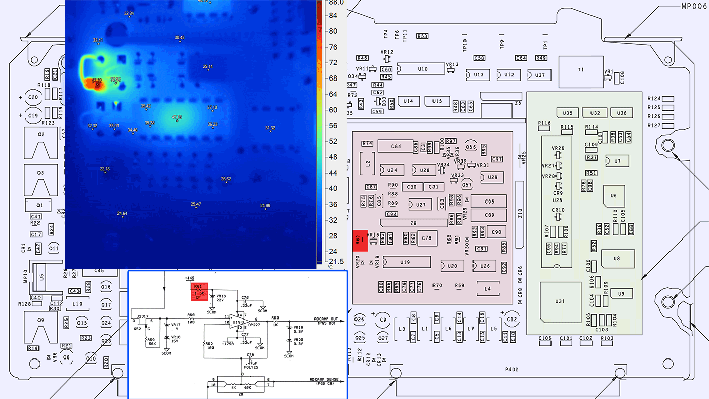
Quick investigation revealed suspicious heating in resistor R61. This resistor connects +44S high voltage power rail to ADC amplifier opamp OP227. Nominal value for resistor is 1.5 kΩ. I can see little tantalum capacitor sitting at the opamp power pin after this resistor, so excessive current would flow in resistor if the opamp or tantalum capacitor are shorted to ground. Very old tantalum capacitors are prone to failure, especially when they are sitting on high voltage rails which can see relatively high current. Typical mode of failure in tantalum capacitor is developing high leakage (or low resistance across terminals, in other words). This high leakage cause excessive current draw and accelerated heating of the capacitor, often resulting in meltdown, fire or explosive unscheduled disassembly. In modern applications tantalum capacitors often used with 50-100% specification derating for the applied voltage.
Original Analog Devices OP227 rated for ±22V supply voltages is now long gone and even datasheets for it are obsoleted. Close modern replacement would be perhaps Texas Instruments OPA2227P or Analog Devices AD8672. Analog Devices chip is available only in SMT packages and just like TI part supports only ±18 V supply range. TI OPA2227P dual opamp is not pin-compatible with original OPA227 DIP14 part, so some leg twisting would be required.
After fixing A11 and A8 board Hulk-3 calibrator is operational to Grade D, per Table 1.
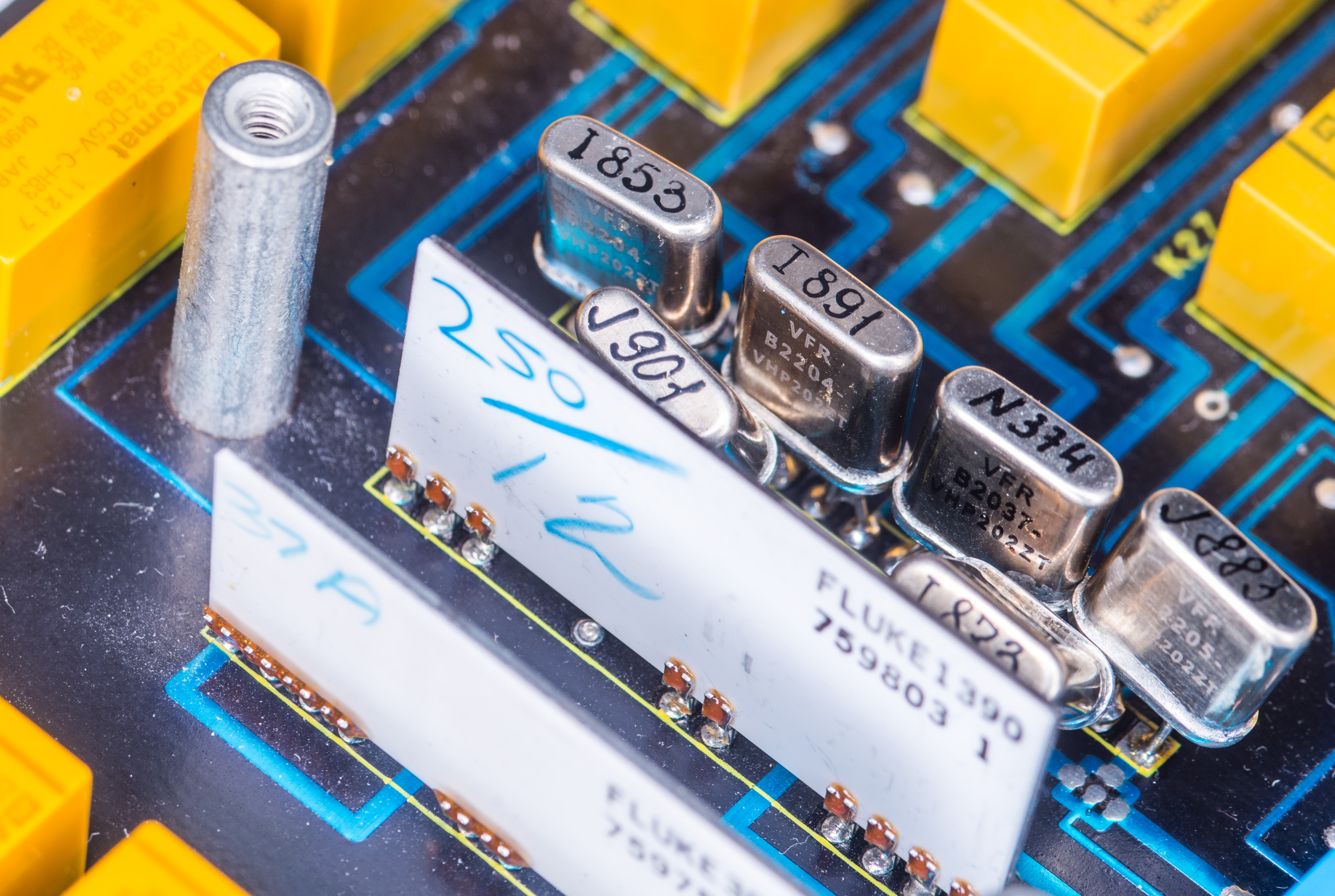
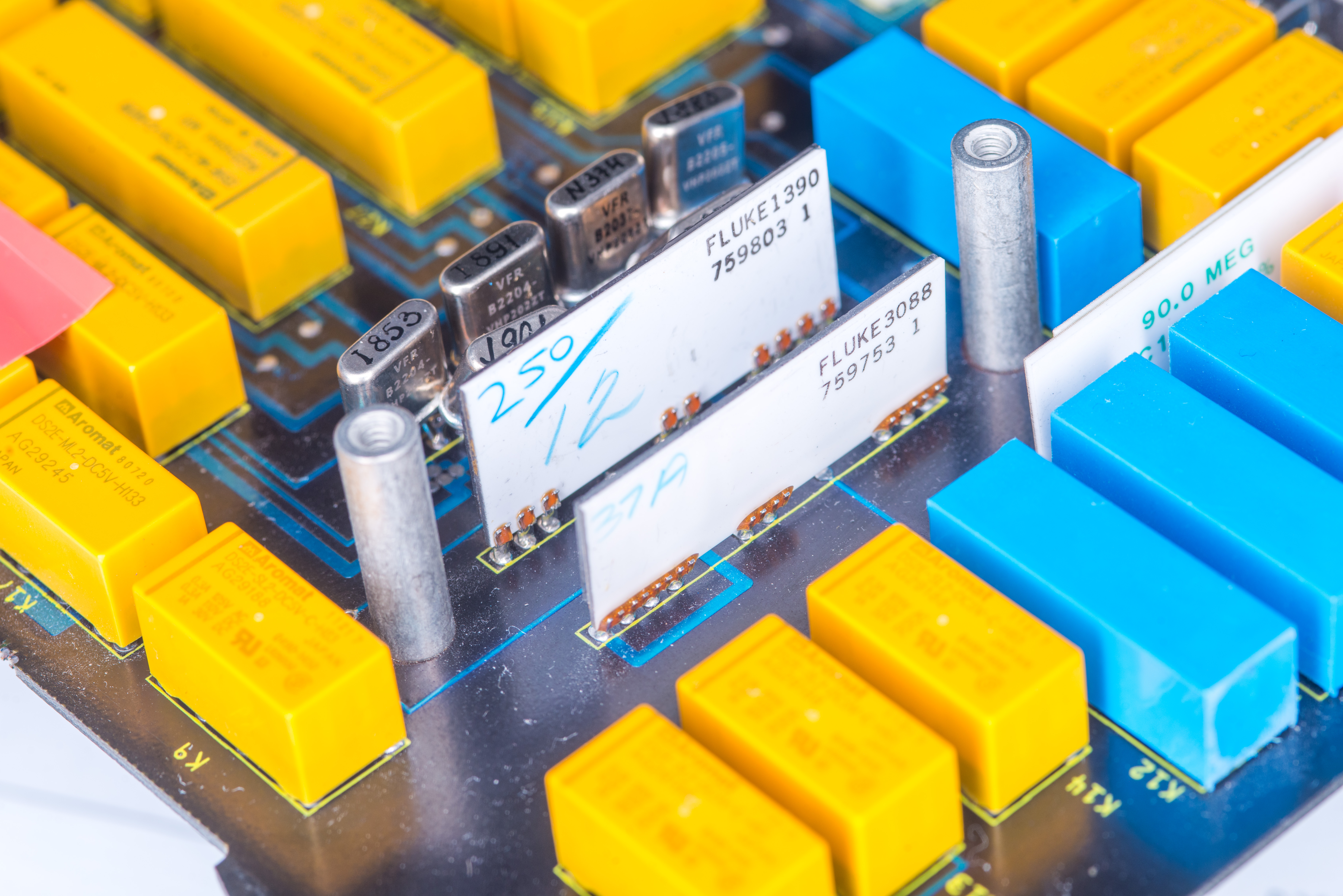
A9 OHM calibration PCBA
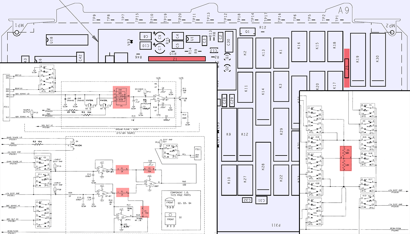
This is Fluke 5720A version OHM CAL board.
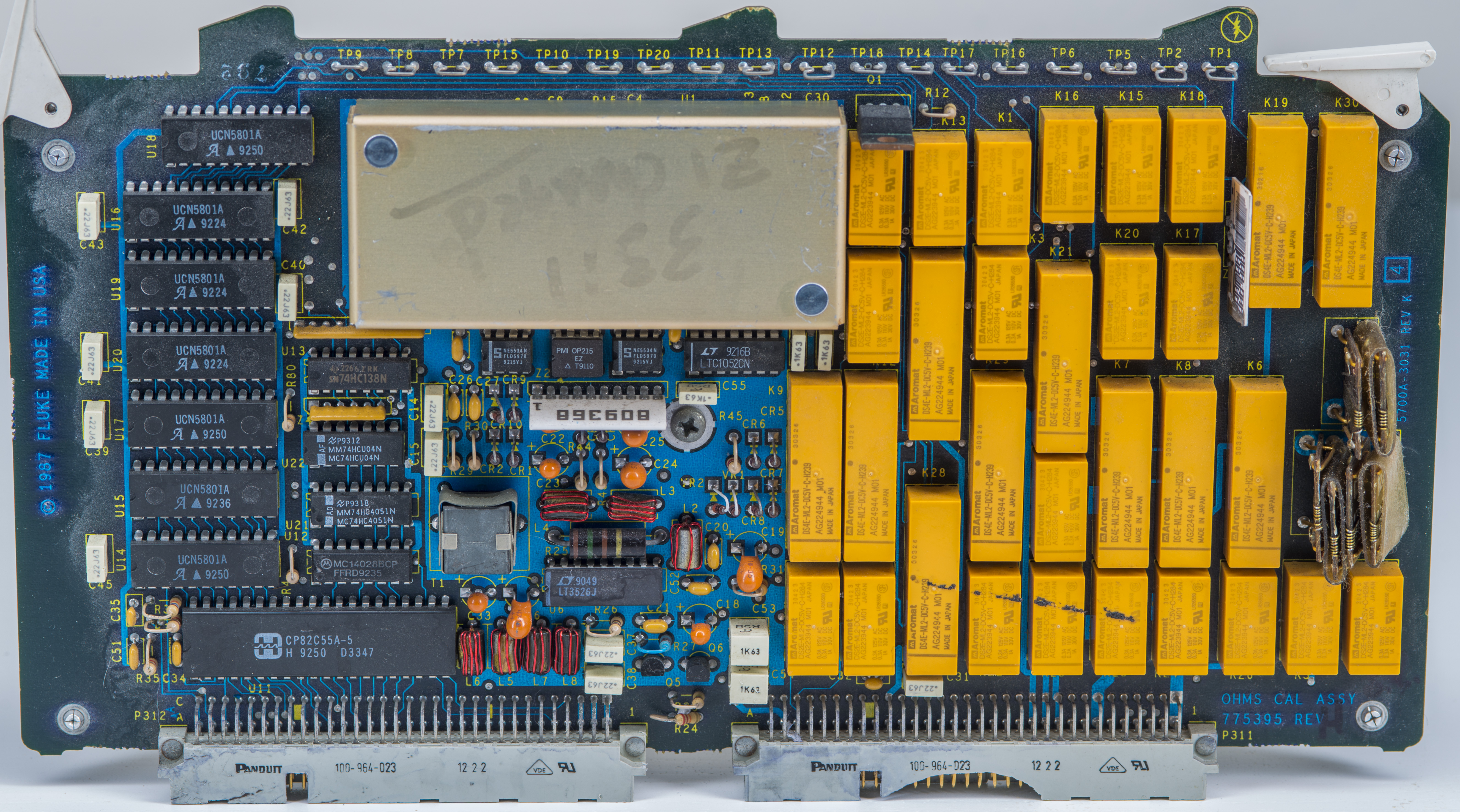
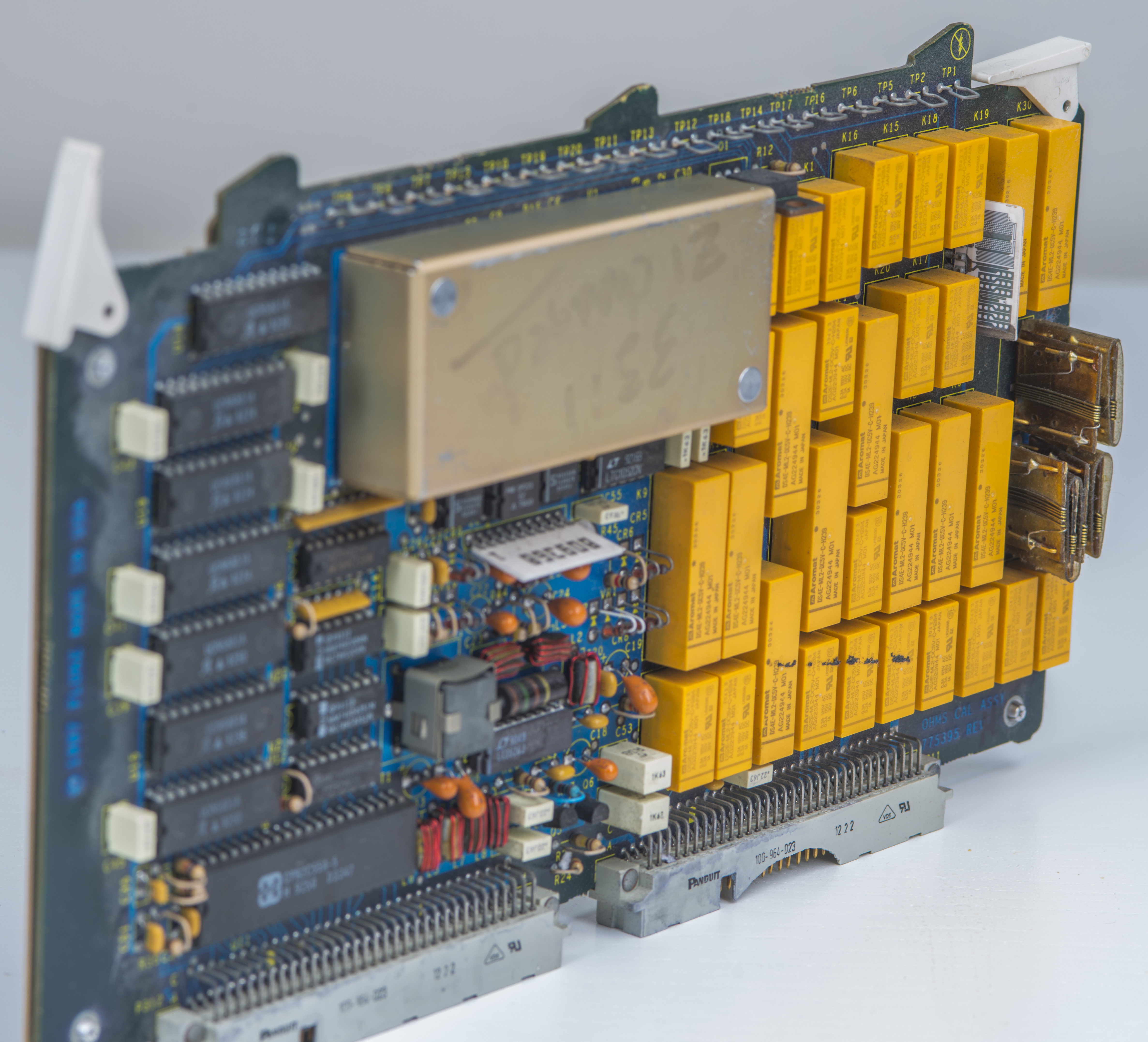
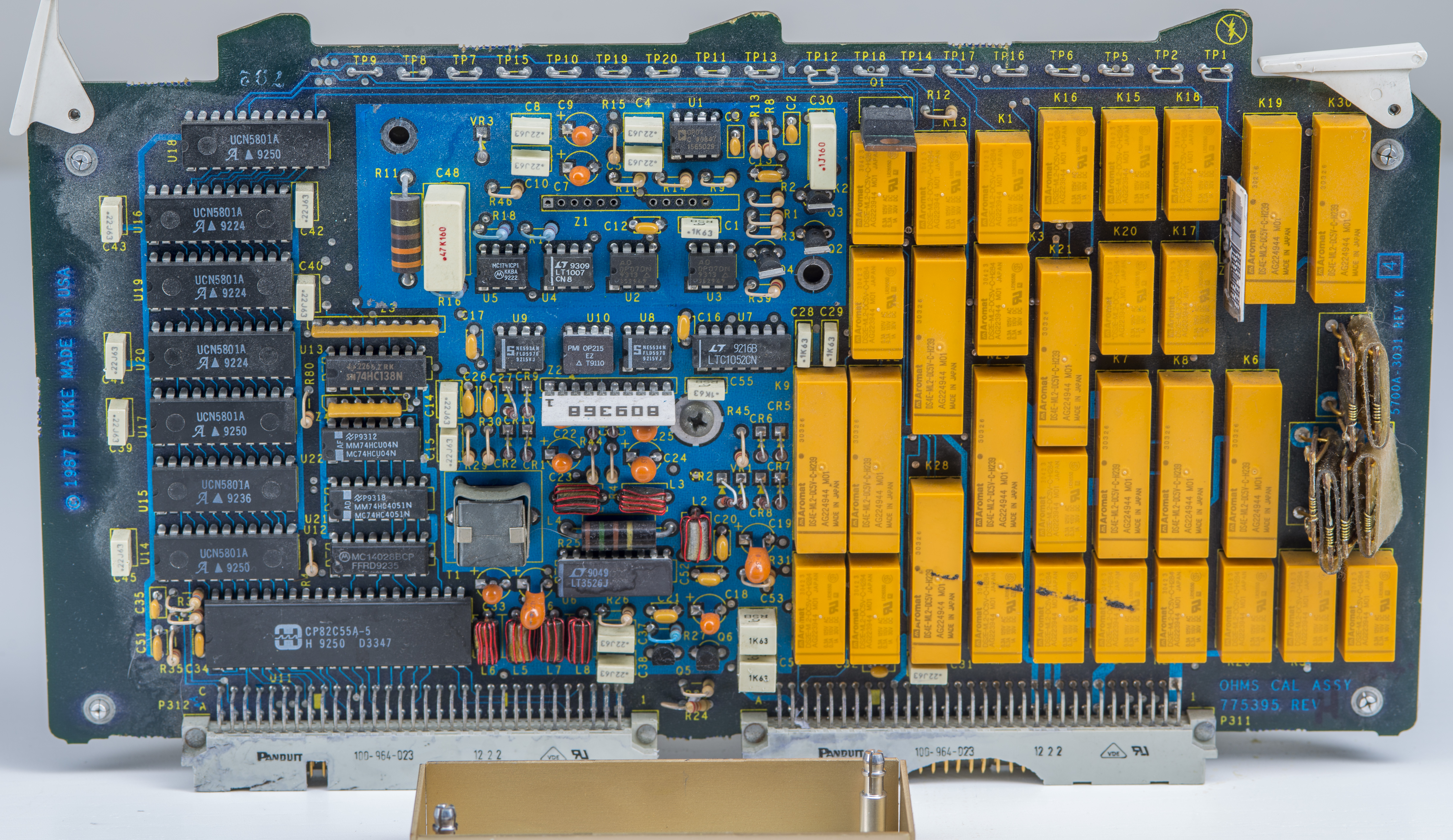
Here we can see missing Z1 network under the cage. It will be interesting to retrofit replacement…
This network is used for differential amplifier and has next elements:
| Network resistor Z1 element | Nominal value | Pins |
|---|---|---|
| Rx | 1 kΩ | 1-2 |
| Rx | 75 kΩ | 2-3 |
| Rx | 1 kΩ | 4-5 |
| Rx | 75 kΩ | 5-6 |
Second issue is destroyed reference 10k/90k network.

| Network resistor Z5 element | Nominal value | Pins |
|---|---|---|
| Rx | 10 kΩ | 1-2 |
| Kelvin junction | 0 Ω | 2-3 |
| Rx | 90 kΩ | 3-4 |
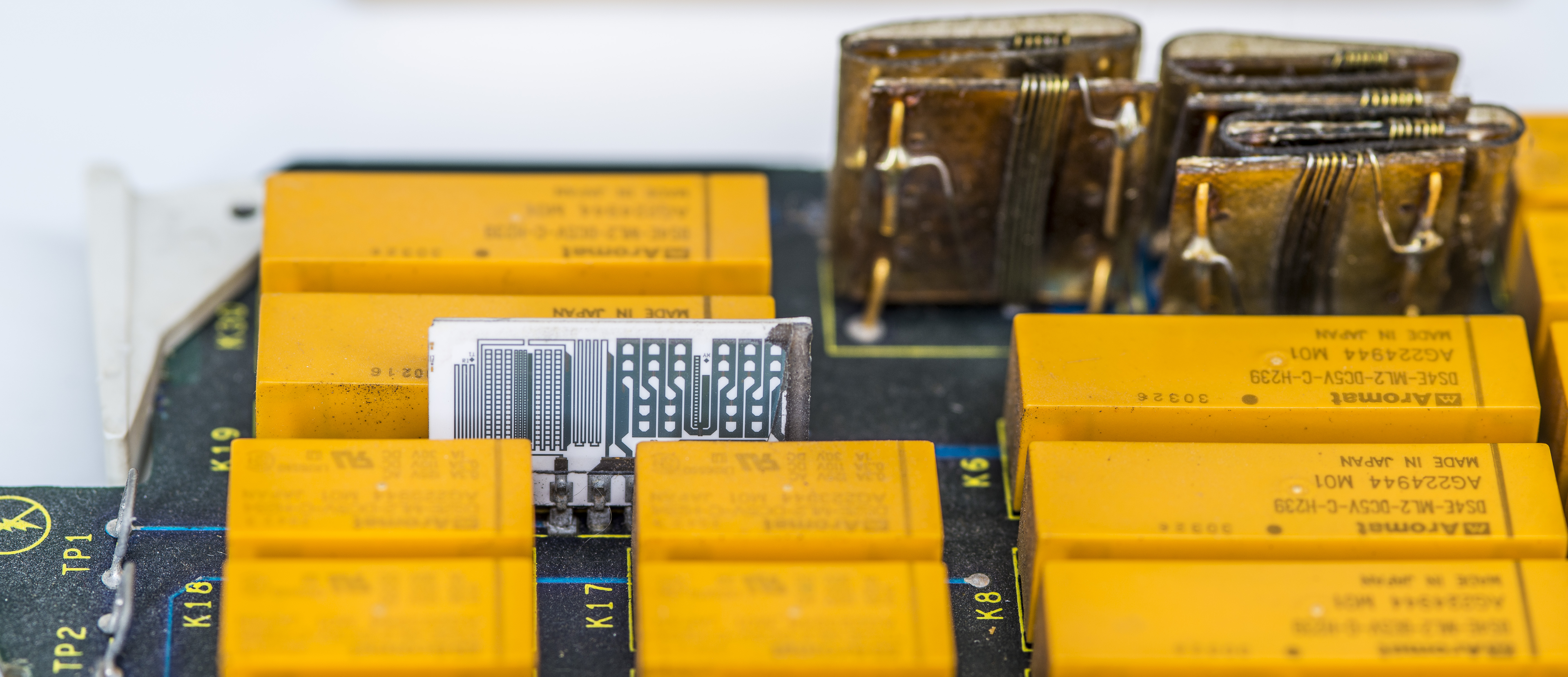
Refabricated resistor network out of discrete PTF56 and similar spec resistors for initial testing:
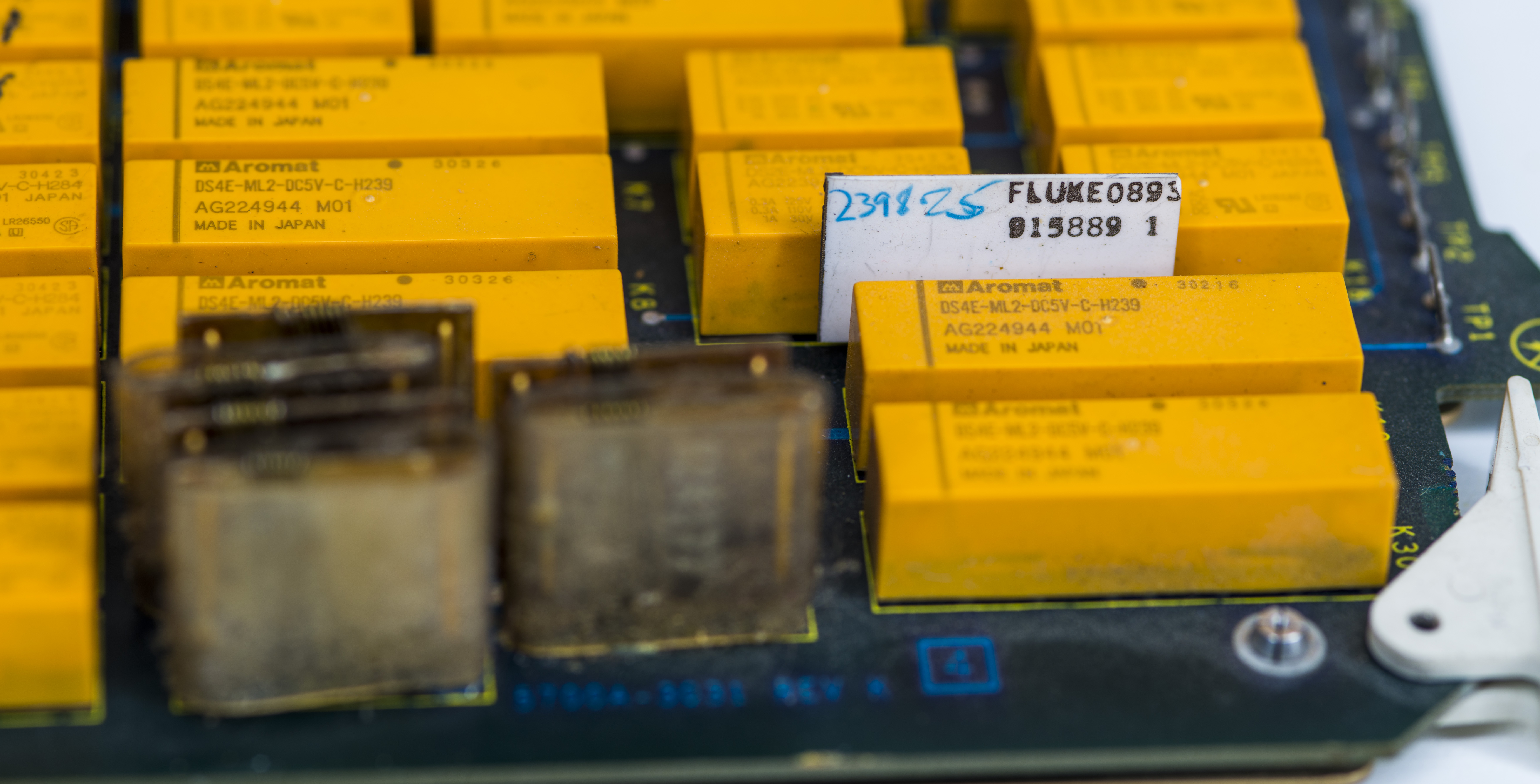
A10 OHM main output PCBA
This board was acquired back in 2018 to donor Z1 resistance network to repair A10 in my primary calibrator after earthquake struck Taiwan and caused some damage. It also had missing relays and relay driver.
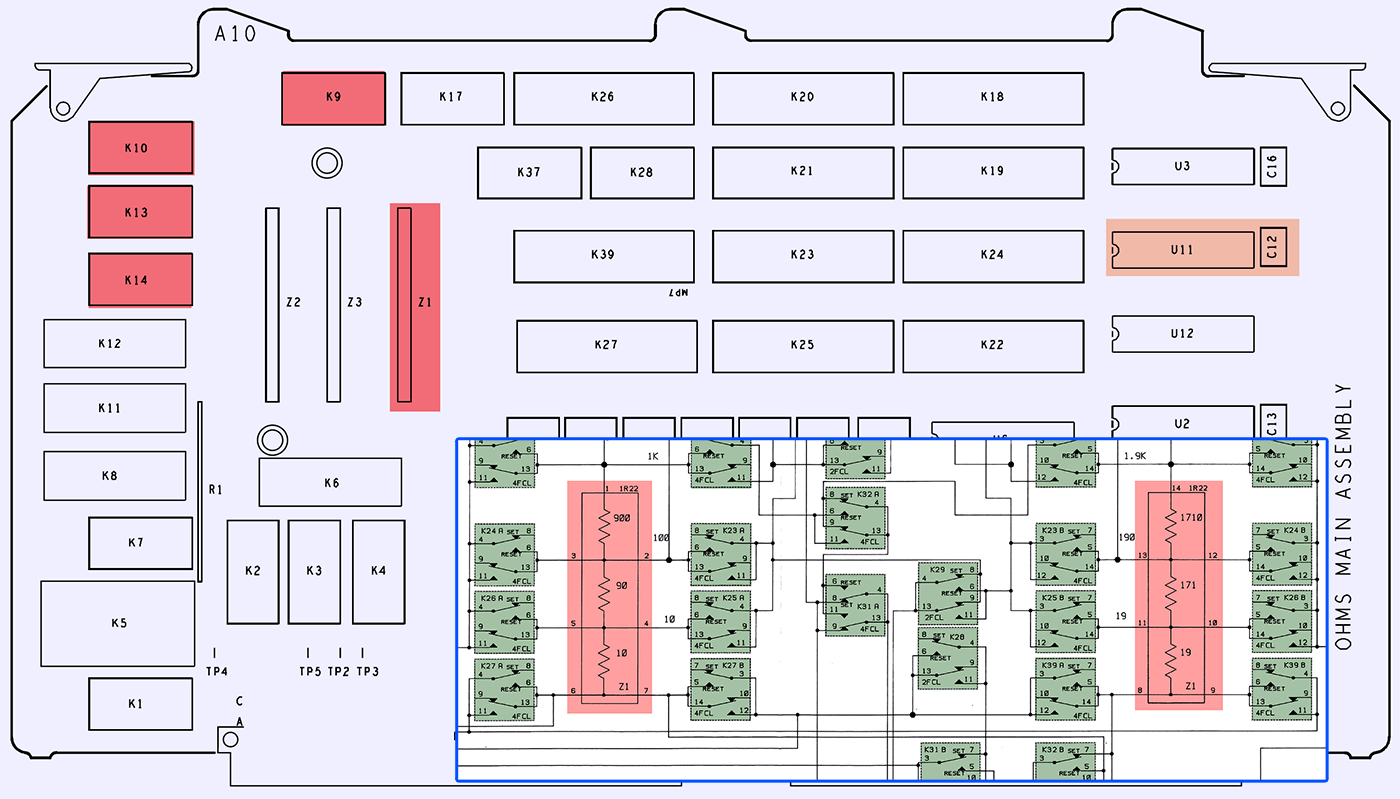
Otherwise untested if any other issues.

Now at this point Hulk-3 calibrator is operational to Grade E, per Table 1.
Summary on spent resources
This project took about $6k USD just in parts, so it does not make financial sense to go down this road. It will be a while till this investment pays for itself, but there are many benefits with 24/7 available multiple 7½ precision calibrators for analog design and various experiments.
And everything started with just innocent buy of 5700A A11 PCBA for $200 to tinker with. Who knew that idea to make stand-alone LTFLU reference get converted into this build? “Volt-nutting” at it’s finest, as even not every calibration lab actually own fully-featured 5720A.
Fortune favors the bold. Perhaps hobbyist with that level of commitment could already buy used and fully working Fluke 5700A, which could need only minor repairs (hopefully). But that was not the goal of this xDevs.com project. It is more interesting to understand (and share via such article) what goes into design of high-performance instrument like Fluke 5700/5720A series multi-function calibrators, with hands-on approach during complex repair tasks.
Discussion about this article and related stuff is very welcome in comment section or at our own IRC-chat server: irc.xdevs.com (standard port 6667, channel: #xDevs.com). Web-interface for access mirrored on this page.
Modified: June 14, 2023, 12:19 a.m.