Contents
- Intro
- Turbo Boost 3.0
- Cooling compatibility
- STEP 1 – Prep your bench
- STEP 2 – Get card ready
- STEP 3 – Power limit overrides
- STEP 4 – GPU Voltage trim-pot mod
- STEP 5 – Memory voltage trim-pot mod
- STEP 6 – PLL Voltage trim-pot mod
- STEP 7 – AUX Voltage trim-pot mod
- STEP 8 – Remove thermal protection
- STEP X – BONUS
- Voltage scaling and ’1.25V limit’
Intro
Sure all of you already read numerous GeForce GTX 1080 reviews, but some still may be left thinking – “what’s about real overclocking, how far this puppy can go with watercooling/subzero cooling?”. It’s time you find out this. Performance boundaries are pushed once again, possible once more with arch changes and latest 16nm TSMC process node technology upgrade. Most of our readers already know all key specifications and performance figures of reference GTX 1080 cards, so I’ll not bother you with that and we go straight to overclocking the new cards.
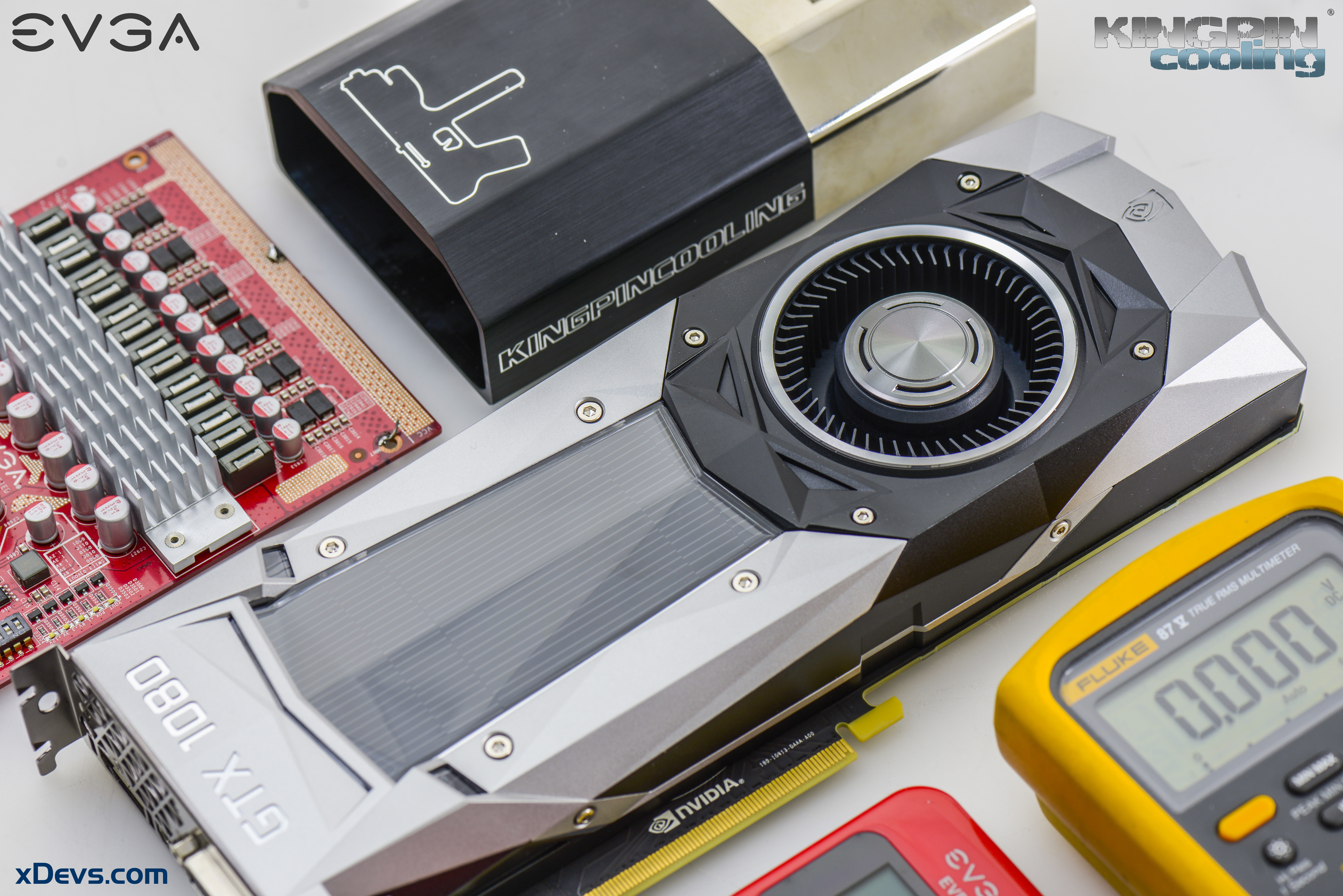
Image 1: Introduction to GTX 1080 overclocking
This guide is evolution of my usual “uncork series”, with all good traditions set by previous guides:
- Reference GTX 680 – Uncorking KEPLER
- EVGA GTX 680 Classified – Uncorking guide
- Reference GTX 780/780Ti – Big KEPLER
- EVGA GTX 980 Ti K|NGP|N OC Guide
- Removing power limits on any NV card
- Using Raspberry Pi to control your VGA VRM
Let’s study plain reference EVGA GeForce GTX 1080 which is also called “founders edition”. This is the baseline card, which we all get to know first before going any specific custom designs.
No doubt, modifying your GFX to for these kinds of results require bit of above-minimal soldering skill knowledge and cold mind. Surely, pro overclockers who are into this sport already have their EPOWER setups handy, so main audience of this guide is not them. I’ll still omit obvious things like how to probe voltage/resistance with multimeter, what is trimpot and how to solder, as these things were explained over the internet thousands times already and easy to google. If you need more info – check previous guides, linked in References section.
As usual, you are on your own when doing even little simple mod. If you card/system burns in flames or just simply stop working, do not try to RMA it or expect a support from manufacturers. Anything below this paragraph in this article is NOT covered by any kind of warranty, and provided AS IS only for education purpose, without support from manufacturer or NVIDIA. So yes, “don’t try this at home”. Any RMA attempt of soldered card is easily diagnosed today and will be rejected.
Okay, let’s find out what color of smoke is hidden inside those Pascal 16nm GPUs! :)
Turbo Boost 3.0
Before we dive, let’s chat a bit about new Turbo Boost thing. On previous Maxwell generation we had three main levers for GPU frequency – voltage, temperature and power consumption. To maximize GPU clock all these conditions must be below limits. Now on Pascal cards the overall concept of GPU controls is still exactly the same, but some of new controls for finer adjustment were added.
Different ways of overclocking
There are two main ways how power users overclock their hardware. Few words about this are necessary to further comply with overclocking approach on Pascal GPUs.
Max performance for everyday use – users who mostly care about practical overclocking fill in this method. This means getting most of performance possible with keeping low power management, low acoustic noise levels and reasonable power consumption. Such users often use aftermarket cooling, like water-blocks to get most from the card while keeping maximum temperatures low. For this case new Turbo Boost 3.0 might be helpful to uncork those little bits of performance left in card.
Max performance at all costs – this is where hardcore benchmark and extreme overclocking folks lurk. Usually involves subzero cooling, completely removing thermal limitations from the card operation. Power limit modifications help to avoid hitting performance cap from the power monitoring. Avoiding worry about temperatures and power simplify things a lot. And since for this case we just want maximum performance at all times, there are no benefits from Turbo Boost 3.0 here.
Now with this short intro of both cases we can get a grasp on new controls. On Pascal now it’s possible to adjust not only GPU clock offset to the all GPU states, but adjust offset for every specific VID range. As part of power management tech on NVIDIA cards since very first GeForce cards, GPU have ability to control its voltage. According to different GPU usage levels power regulator output is adjusted on real-time to get lowest possible voltage for desired frequency. This translates to a voltage/freq relationship, which can be shown as table of values with multiple points.
On pre-Pascal GPUs we can add offset to desired GPU frequency which is being applied to all frequencies in V/F table. But actual maximum frequency of specific GPU can be either lower on specific voltage points (this will make card crash and get stability errors/artifacts) or higher (meaning card could be faster, but capped by fixed GPU offset/volt table). Turbo Boost 3.0 on Pascal now allows you to control each point, to get the most performance possible. So new version allows you to play with everyday overclocking knobs in more precise manner, but does not change much for extreme “all-out” overclocking cases.
Cooling compatibility
Many of enthusiasts always worry if their current water/chiller or LN2 cooling system will still be useful for fresh new hardware, such as GeForce GTX 1080. Worry no more, mount hole locations and clearance is exactly same as 680/770/780/980/980Ti/Titan reference cards. Previous generation GPU coolers will fit new card fine, if not constrained with VRM area coverage.
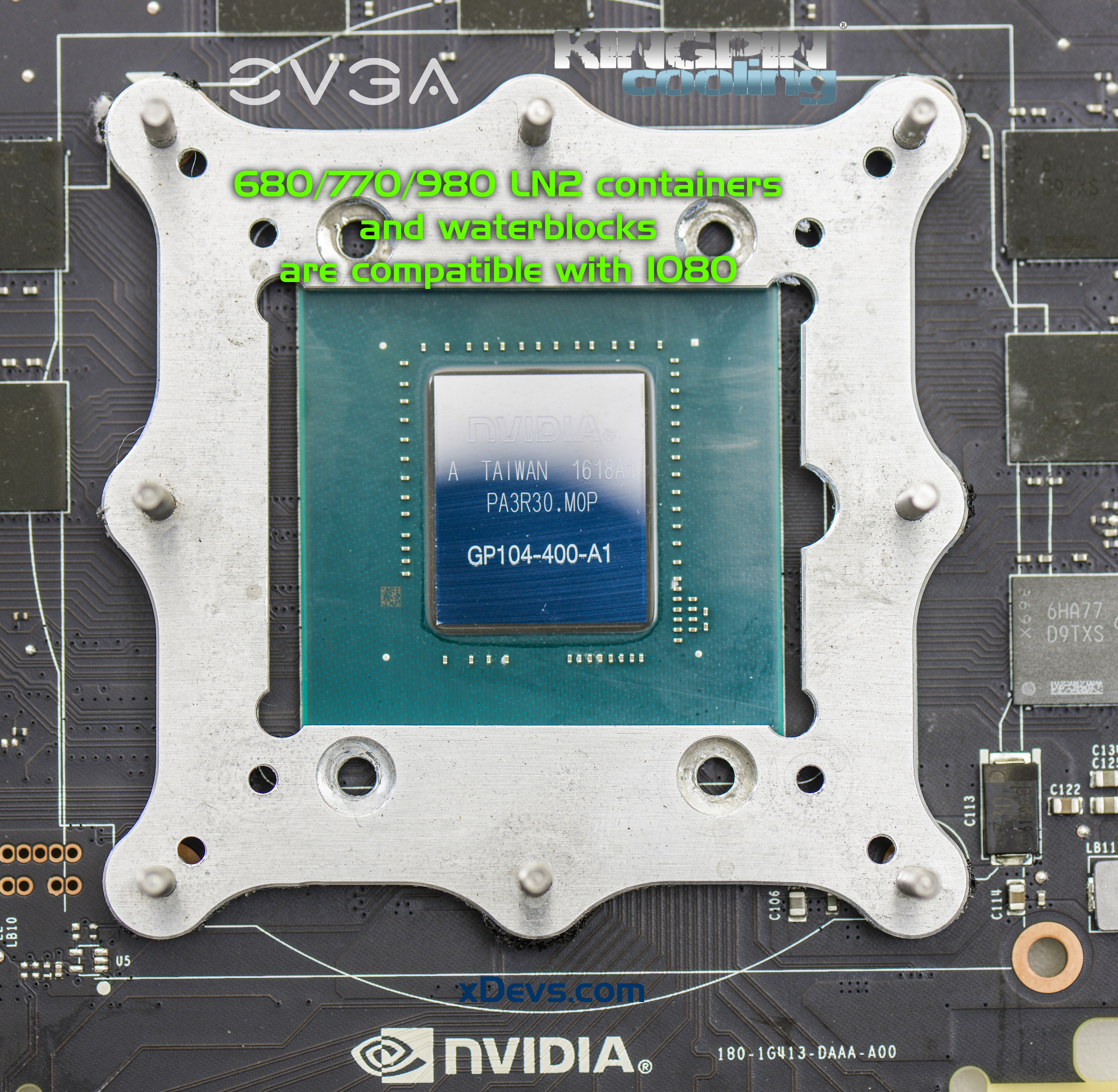
Image 2: Cooling hardware overlay on GPU area
New GPU does not have metal shim around the core anymore, so be extra careful mounting your cooling solution and keep surfaces parallel. Cracked GPU silicon never did any good to card’s functionality.
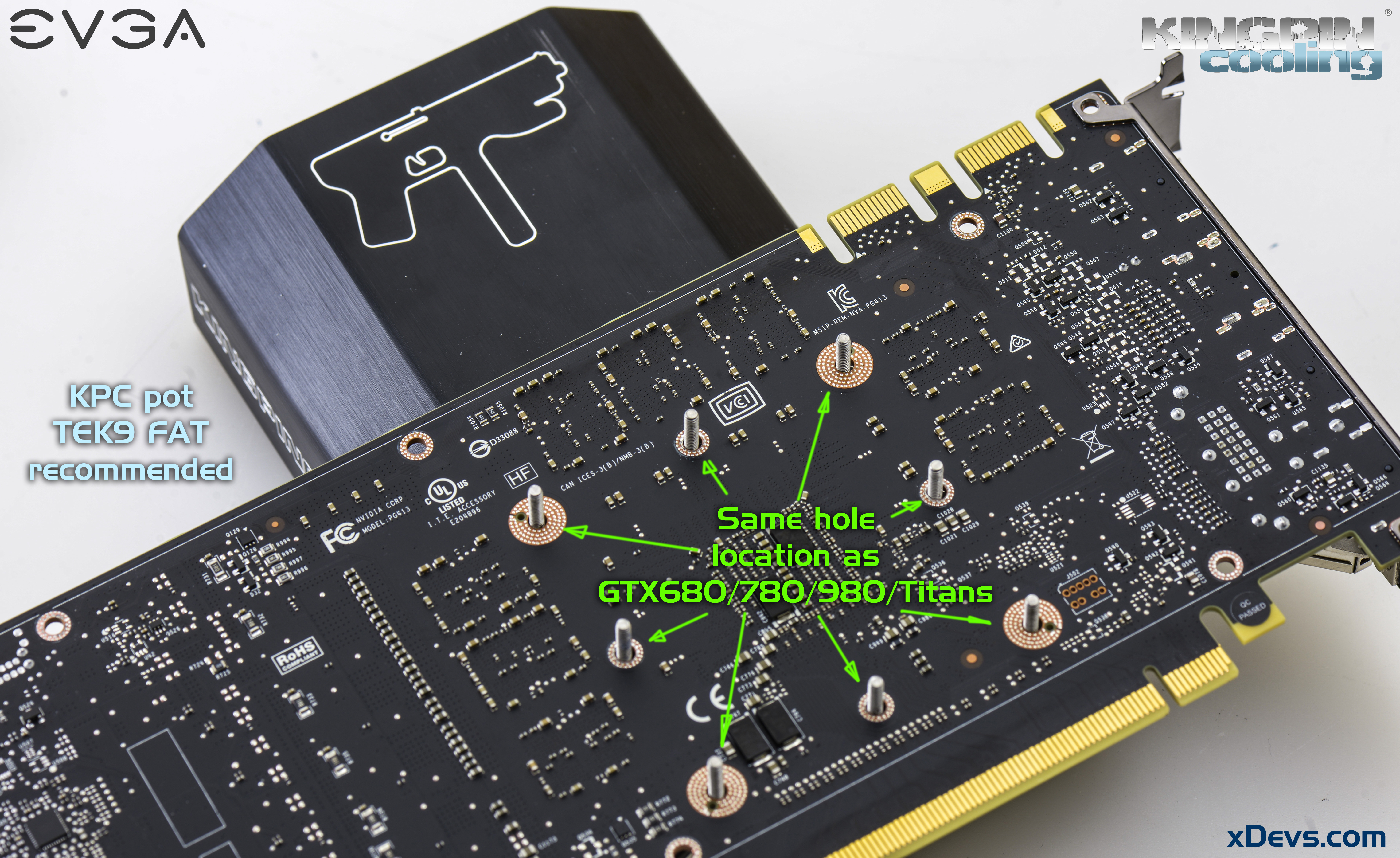
Image 3: 8-point mount of LN2 container on GTX 1080
Best to have full 8-points brackets to ensure good and even mount pressure across all GPU sides. It’s compatible with all TEK9 FAT and TEK9 SLIM containers and can be bought separately on Kingpincooling.com shop
STEP 1 – Prep your bench
Will need set of common tools for successful modding of reference GTX 1080 card. Modification of GTX 1070 FE can follow same technique, as layout of both reference cards almost identical.
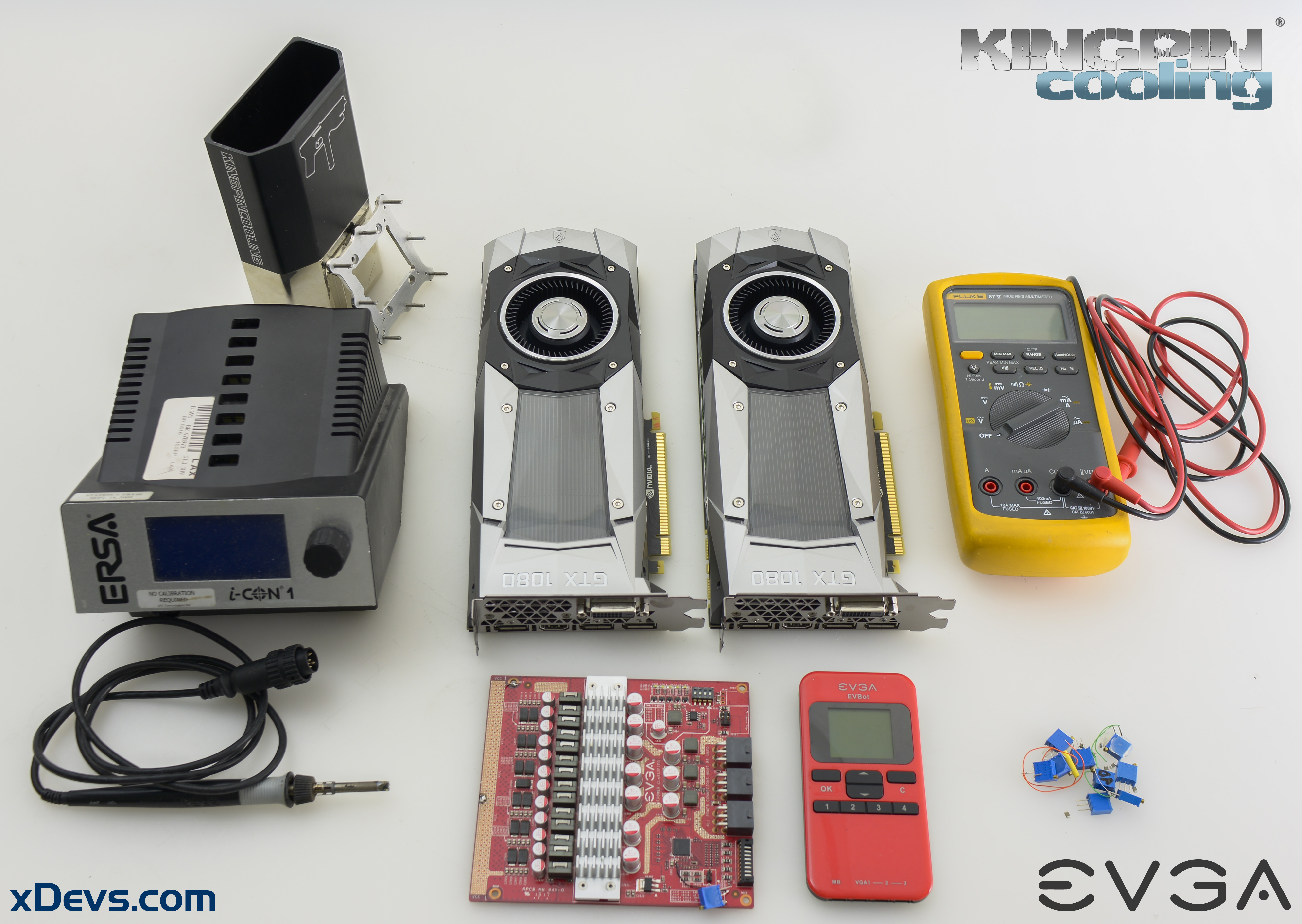
Image 4: Cards, DMM, soldering gear, parts and LN2 pot ready
- Card itself. Here are two EVGA GEFORCE GTX 1080 FE (08G-P4-6180-KR) cards to play with.
- 2 × 1 KΩ multi-turn VRs (trim pots) for memory and GPU vmod.
- 1 × 1 MΩ multi-turn VR (trim pots) for 1.8V vmod.
- 1 × 100 KΩ multi-turn VR (trim pot) for PLL mod.
- 3 × 10 Ω chip resistors, 0805 size. Example from Digikey, Mouser, Farnell DE for power limit mod.
- 25-45W soldering iron for trimpot mods, 80-120W for EPOWER.
- Roll of 28-32AWG insulated wire
- Soldering FLUX
- Kingpincooling TEK9 FAT
- DMM (I use fancy handheld Fluke 87V and high-performance Keithley 2002, but any 10$ DMM can fit needs of this guide)
- Low-ESR capacitors (2.5 or 4V rated, 680-820uF , etc) if you like to juice things up, but not required.
Image 5: Trimmer resistors and ceramic capacitors example
Since EPOWER connection to card this time is not covered, no need to use high-power soldering iron and pretty much any soldering gear you have on table will fit the task well.
I had used ERSA iCON-1 soldering station with to cover all below. 102CDLF2.4 tip covered all trimpot mods for this guide, with temperature set to 290 °C. Before starting with soldering, clean the usual mess on table, get all tools checked and ready, turn on enough lights to clearly see tiny parts on PCB. Worth to ensure enough space around, so you don’t knock other stuff by accident. Your setup shortly can look like on Image 6.
Image 6: Removing backplate covers and getting card ready
Also worth to take a close look on PCB layout from both top and bottom sides, to get familiar with location of key components and design. Two 105 MPixel resolution images will surely help you to do so:
Image 7: 105 megapixel GeForce GTX 1080 photo, front top side
Design is fairly similar to previous x80 cards from NVIDIA, such as GTX 680, 980. We have GPU in center with eight Micron GDDR5X memory ICs around, main power converters for GPU and memory at right side of the card, powered from single 8-pin MiniFit JR plug and usual display output layout with three DP ports, HDMI and DVI-D. There is no VGA analog output, so VGA-DVI passive adapter will not work with Pascal anymore. You still can use DP-VGA or HDMI-VGA active (with converter IC inside) adapters if you really want to.

Image 8: 105 megapixel GeForce GTX 1080 photo, rear bottom side
On the bottom side we just have some passive components and auxiliary circuitry. NVIDIA FE cards are equipped with very thin backplate covers. Brief look on the fansink..

Image 9-10: Heatsink after removal from the card
It’s similar to previous generation cards with blower fan and finned aluminum heatsink. To improve thermal transfer from GPU die copper vapor chamber is soldered on the base, just like on GTX 580/590/680. As you will see later, better thermals are crucial part of Pascal’s performance scaling.
And final overview of GPU package and used memory:
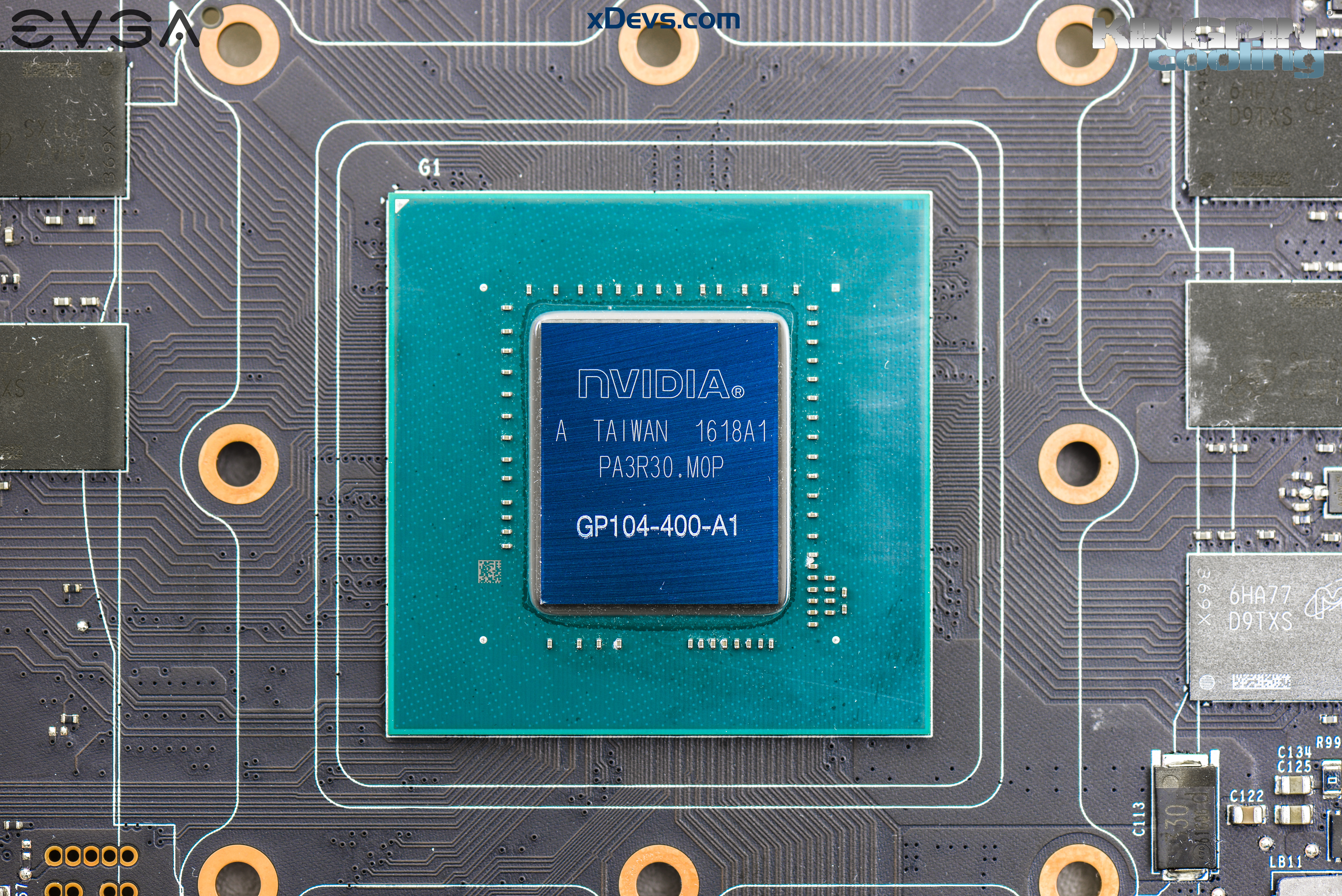
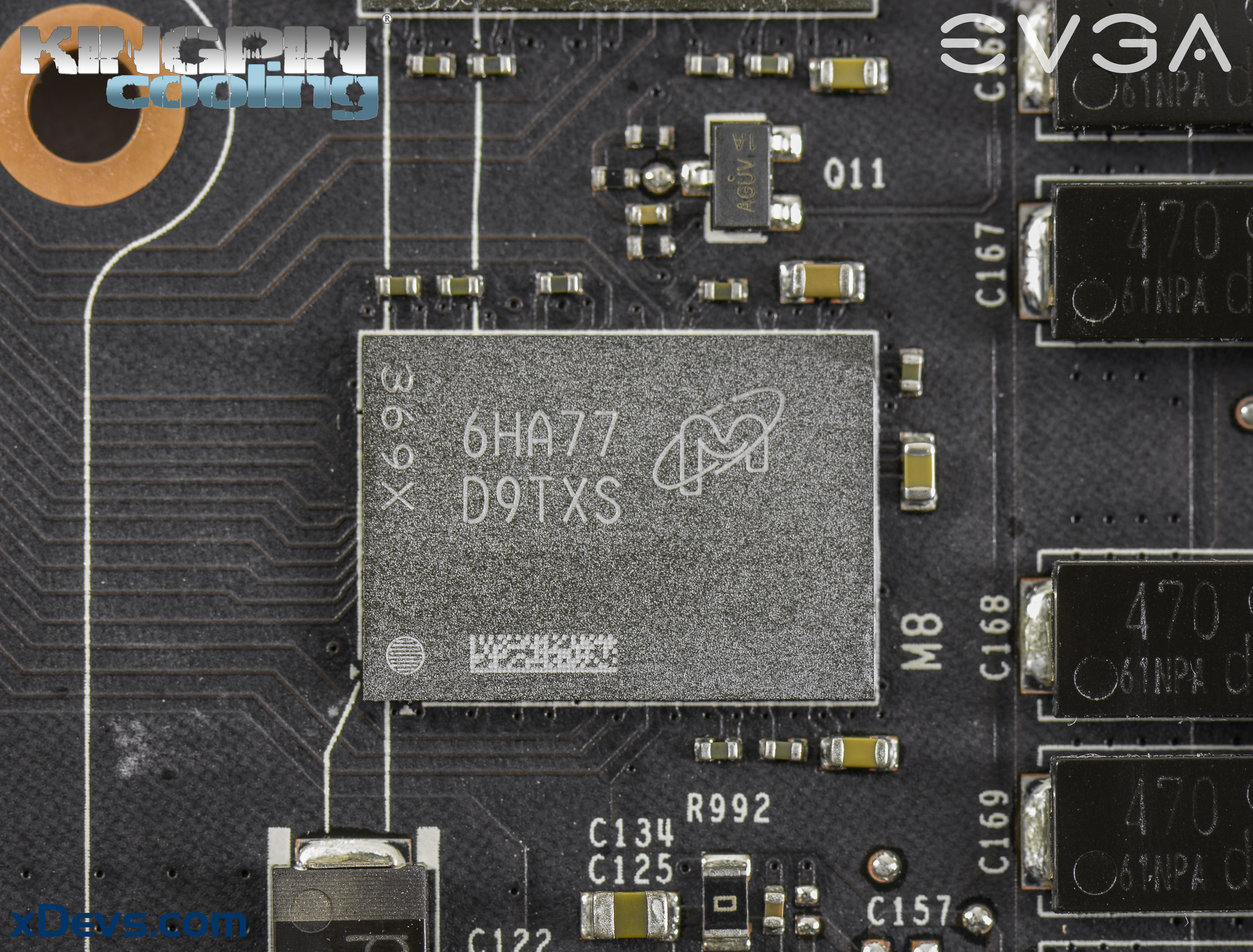
Image 11-12: NVIDIA Pascal graphics processor and Micron GDDR5× 10GHz memory
GPU bears GP104-400-A1 marking, which tells you it’s mid-range 104 series processor (to remind you, GTX 680 was GK104, GTX 980 was GM104), silicon revision A1. It was manufactured by TSMC Taiwan in 18th week of 2016. GPU area is similar to previous generation processors, but have much more transistor gates due to much smaller 16nm FinFET node process. There are some 0201 decoupling capacitors around GPU die to help with power delivery. No hidden jumpers, traces or test points are visible on the package elsewhere.
Micron memory is production sample already, with BGA code D9TXS. Using Micron’s FBGA & Component Marking Decoder we can easily get chip part-number: MT58K256M32JA-100:A which according to datasheet is 8Gb: x16, x32 GDDR5X SGRAM with rated data rate at 10.0 Gbps. Currently this is the only GDDR5X memory available on the market. Technically it’s QDR memory, but to keep things simple JEDEC desired to keep GDDR5X name for it, as it’s layout and core technology is similar to well-known GDDR5.
Few more things we can learn from the memory IC datasheet, such as nominal voltage reduction from 1.55V (GDDR5) to 1.35V and requirement of one extra voltage rail – VPP with 1.8V level.

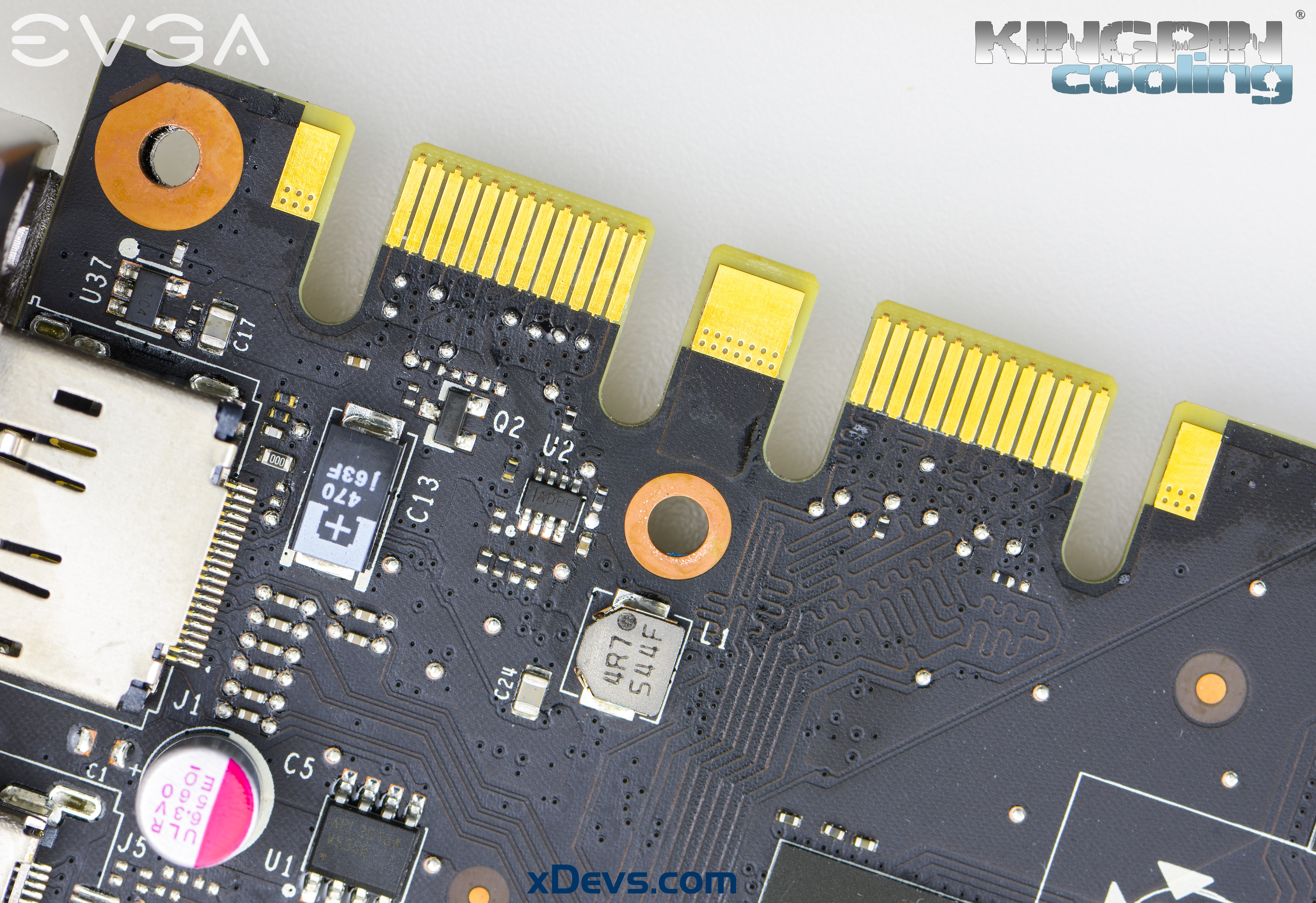
Image 13-14: PCI-express 3.0 and SLI edge connectors
SLI and PCIe connectors look exactly same as before, no magic there. For high 5K/8K resolutions and multi-monitor surround you might want to use new SLI HB bridges, which connect both SLI fingers in 2-way SLI setup.
STEP 2 – Get card ready
Remove cooler from the card, since access to both sides of PCB for modifications is required. This time NVIDIA did not use TORX, so usual Philips and hexagon driver will do just fine. Avoid using pliers as those little components and resistors around are very easy to get damage if tool snaps. You will need hexagon driver to remove nut-head screws which used to hold backplate and PCB together. Better keep all those custom screws in secure place somewhere, so you can put heatsink back after you done if you will decide to do so.

Image 15: Screws after stripping card
Remember, after soldering your warranty will be surely violated, as every RMA center will easily see non-factory soldering specks, even if you very careful. Please, believe me ;).

Image 16: GTX 1080 bottom side exposed
Now graphics card is exposed and ready for some measurements and modifications. I’ll spare our readers from boring part of measuring various points to find out what we need and where different connections go, so we can jump right into good stuff, starting with removing power cap limitations.
STEP 3 – Power limit overrides
Often gamers and users are mistakenly referring to 6-pin or 8-pin MiniFit.JR connectors as 75W or 150W capable inputs. Nothing can be further from truth. These power levels are nothing but just way for NV determine how capable is used board hardware to deliver power. It’s purely imaginary number and have nothing to do with actual power taken from connector nor power input capability. Software and NV BIOS will handle GPU clocks and reduce voltages if measured power hitting programmed BIOS limit (which can be different value than 75/150W!).
So if we just change circuit to report lower power reading, this limitation will be lifted accordingly as well. Also to make sure we are not at any physical limit of power connector itself, check Molex 26-01-3116 specifications, which have specifications both 13A per contact (16AWG wire in small connector) to 8.5A/contact (18AWG wire). This means that using common 18AWG cable, 6-pin connector specified for 17A of current (3 contacts for +12V power, 2 contacts for GND return, one contact for detect). 8-pin have 25.5A current specification (3 contacts for +12V power, 3 contacts for GND return and 2 contacts for detection). This is 204W at +12.0V level or 306W for 8-pin accordingly. Now if somebody tells you that 6-pin can’t provide more than 75W, you know they don’t understand the topic well. It’s not the connector itself or cable limit the power, but active regulation of GPU/BIOS/Driver according to detection of used cables and preprogrammed limits. So how actual power measured?
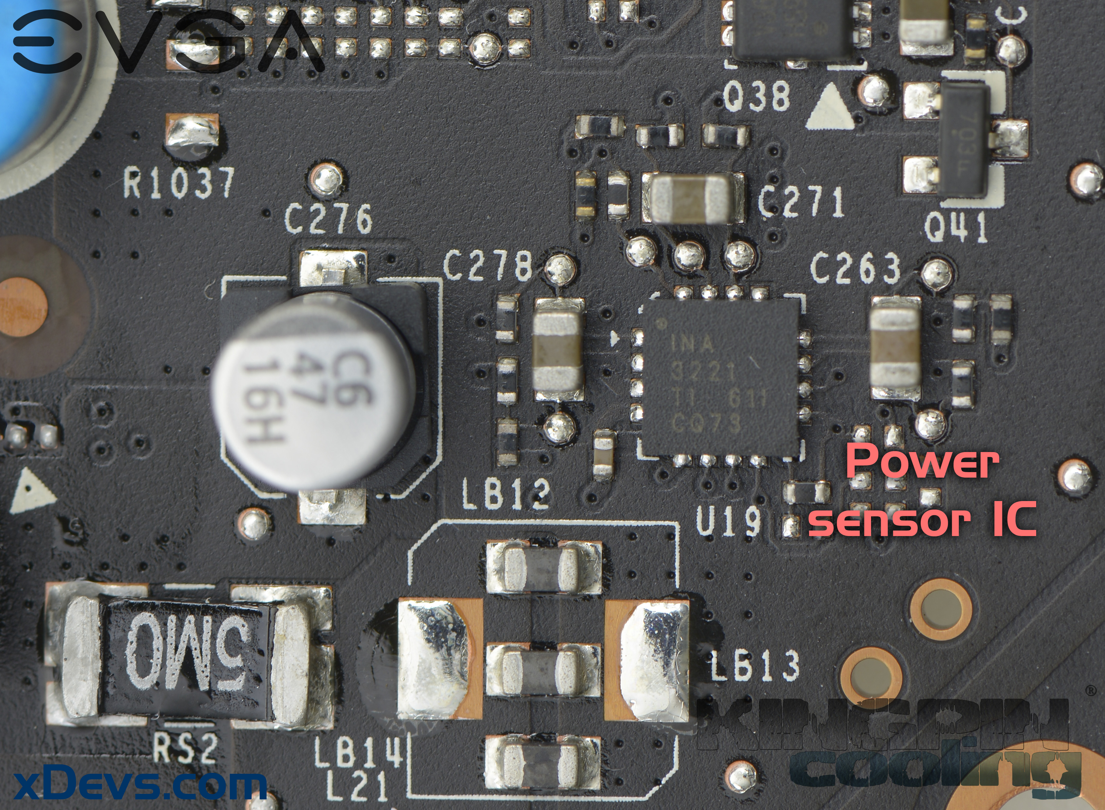
Image 17: Texas Instruments INA3221 location
This card is using already known Texas Instruments INA3221 sensor IC, which is triple-channel monitor able to measure voltage, current and power on +12VDC input rails using just few external components and current shunts. Current shunt is special type of resistor which generate little, but measurable voltage which closely depends on amount of current flowing thru it. Thus card can detect power consumption in real-time and adjust its clock speed and performance automatically to keep power within specified envelope.
And since when doing serious overclocking we likely to need more power than actual limit is, here we need to tamper this power monitoring circuitry to report less current flow than actually is.
It sounds more difficult than it actually is, so here are photos to illustrate the mod:

Image 19: Location of current shunts
You can find current shunts which are marked RS1, RS2, RS3 on PCB with black resistive element in center and often with R002 or R005 or 2M0/5M0 mark on top. Sometimes there are no marks, but look is always very similar. Usually these shunts are located very close to input power connectors before the main VRM circuitry. If we manage to reduce signal from these shunts, then reported power limit will be reduced as well.
Note that earlier version of this guide incorrectly mentioned need to short RS1, RS2, RS3. This is wrong, and will cause card clock to lock at 135MHz. Do not short shunt resistors themselves, but add resistors like shown on photo below. Sorry for confusion.
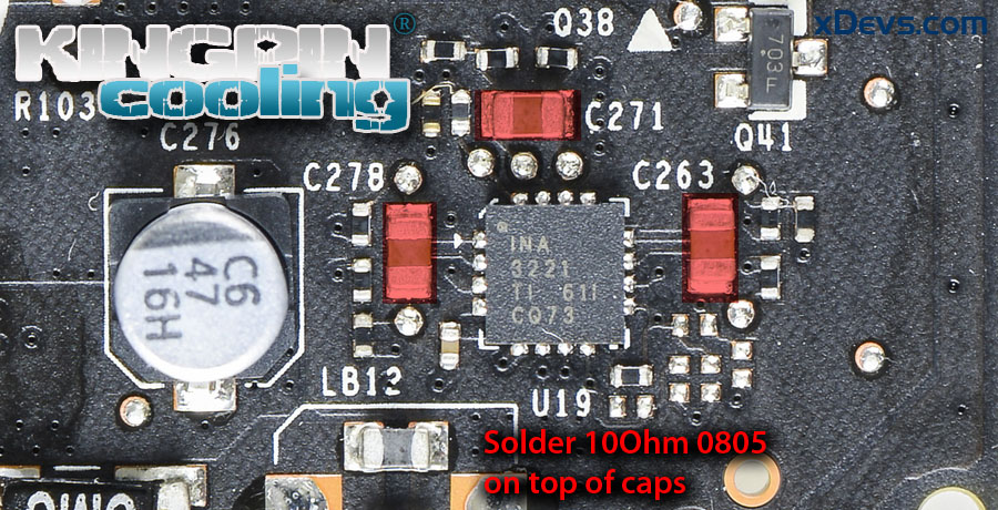
Image 20: Add 10Ω resistors on top of red mark parts
Adding 10Ω 0805 size resistor on top of every capacitor will reduce power levels about x3 times. These chip resistors can be bought in usual electronics shop, or online at retailers like Digikey, Mouser. In worst case you still can use usual thru-hole resistor, but it’s not as convenient and tidy.
This modification is very similar for all other NVIDIA cards, and bit more details covered here and here before.
STEP 4 – GPU Voltage trim-pot mod
First and usually most viable modification is one to adjust GPU core voltage. Often (but not always!) extra voltage can help to get better stability and higher clocks, given no temperature or power limitations are hit. Maximum available voltage thru software only control on reference cards are very limited, so hence you may need hardware modification to achieve higher voltages.
Here’s photo of GPU power controller, which is now UPI uP9511P, instead of ON NCP81174 which we saw on previous generation reference GTX 980 and GTX 980 Ti cards. UPI’s site is really obsolete and lacks of information, so I could only know from layout and probing around that this controller supports at least 6 phases, no digital interface or parallel VID code setting (no array of 6-8 resistors around to set VID voltage code).
Also uPI chipsets are still using purely analog, so there is no firmware for this PWM and all protections like OCP/OVP are done by hardware and external components.

Image 21: GPU power PWM controller
But no worries, by tracing where GPU power signals come around chip voltage sense lines were quickly found. These are two lines from resistors near R1007 and Q510 location. Enough to know for us to do the voltage mod!
Prepare VR’s, in this case one 1 KΩ nominal resistance multiturn variable resistor (potentiometers). I like to use very common blue square 3296 type. There are many electronic components retailers have these available for sale, and it should be easy to find suitable resistors from your local store.
Now remove resistor marked in red box on photo below to enable adjustment on feedback sense.
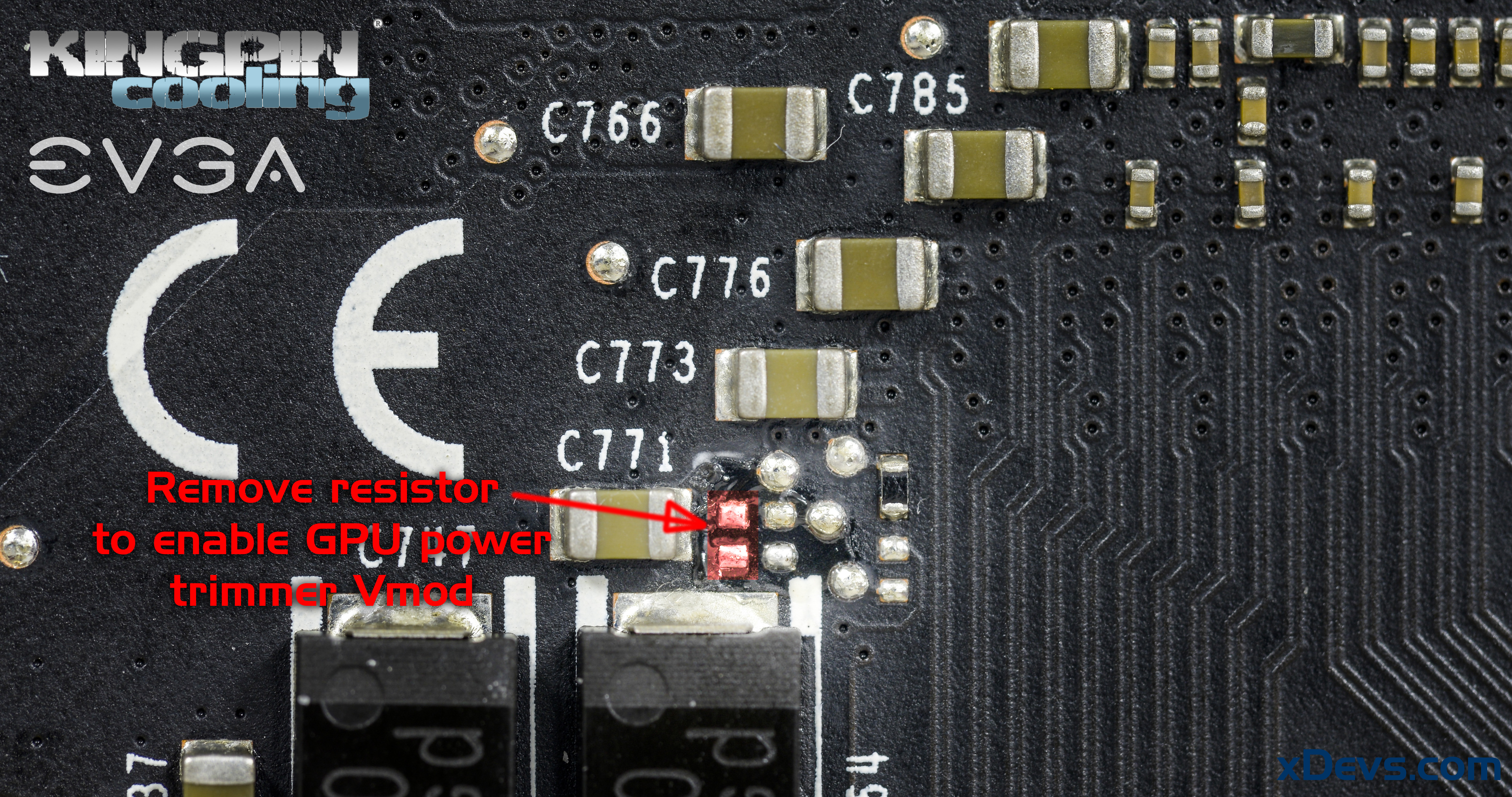
Image 22: Resistor location to remove GPU power control
Without this step voltage will be directed by GPU to VRM connection, and modification would not work as expected.
Glue 1000 Ω trimmer on the PCB like shown on photo below, to make sure it does not rip off or short anything later on. I also used 2-position jumper pins to add ability of disabling mod to get stock voltage on the fly. That could be useful for troubleshooting later. Two AWG32-28 wires will be needed to connect trimmer to specific points.
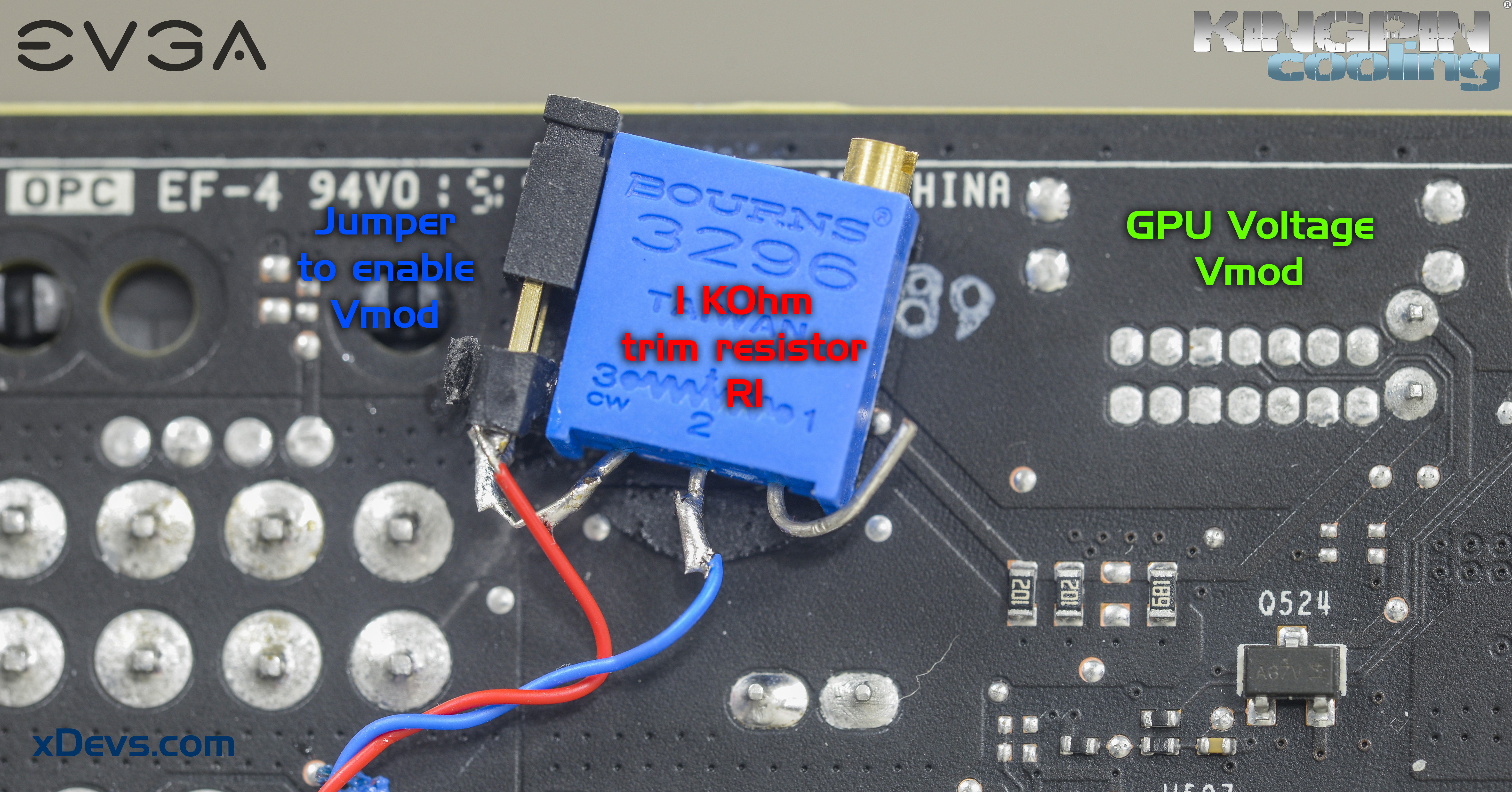
Image 23: Example location of 1 KΩ trimmer
Make sure you set resistor to maximum value (resistance measured by DMM across both wires, not connected to anything), which should be around 1000 Ω. Not a good idea to boot card right from maximum voltage. Solder wires to tiny spots near GPU voltage controller (uP9511P IC on the bottom side of the board).
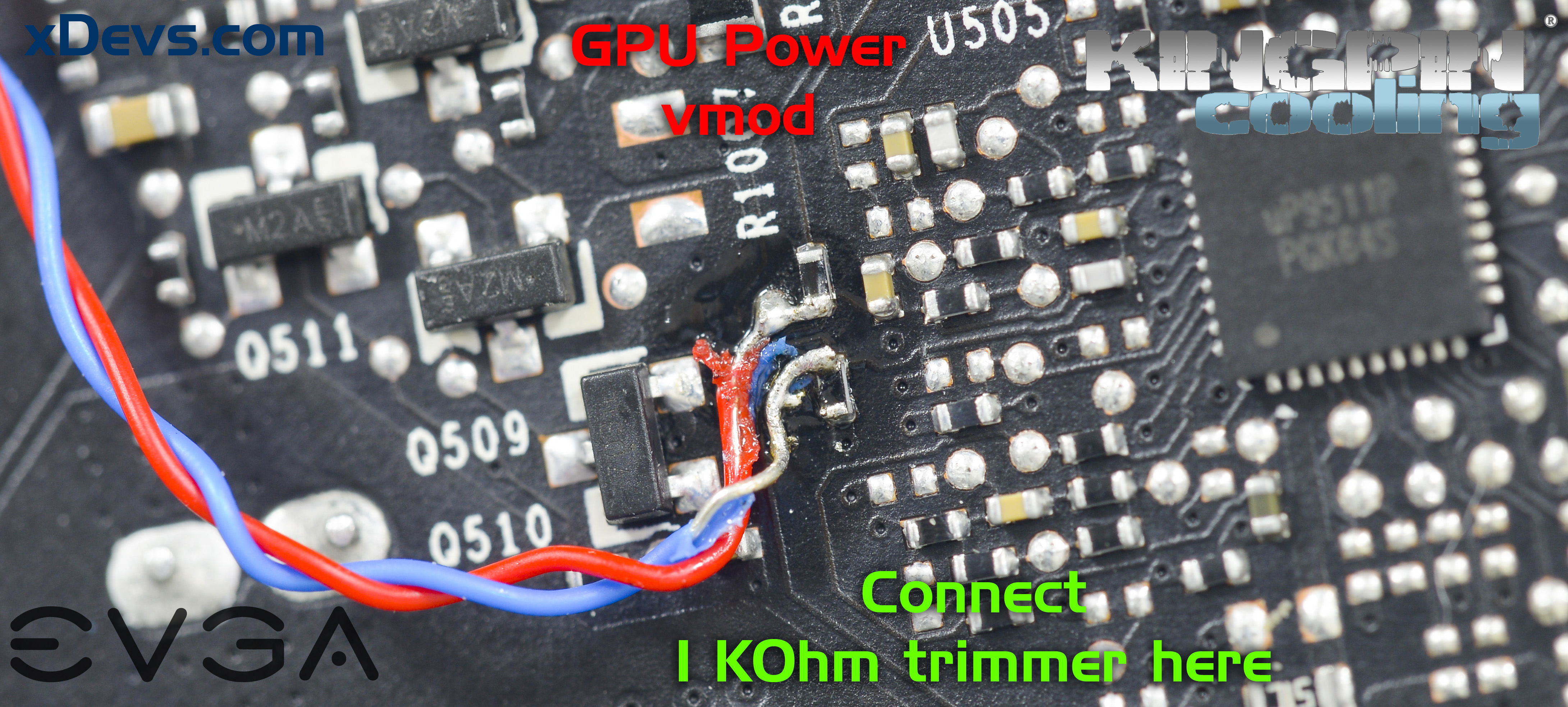
Image 24: Connection points of trimmer to raise GPU voltage
Any wire to any resistor can be soldered, order here is not important, as resistor have no polarity and bidirectional. Just make sure your connection is in same way as on the photo, and that should do it. Overall modification shown on final photo below:

Image 25: Overview of NVVDD modification
Since traces and solder points on PCB are very thin and easy to peel off, make sure you fix the wire to PCB in few places, so it does not move. I found use of few cyanoacrylate superglue drops on areas free from components good enough. This will ensure modification is safely secured and will not rip apart tiny components so easy.
You can go as high as 1.6+V with this kind of modification easily, which is more than enough for Pascal extreme overclocking. However, safer voltages, even on LN2 cooling are rather around 1.3-1.6ish range, as this 5-phase VRM is not exactly designed for high-power/high-voltage use.
Note that GPU resistance on GP104 is very low, opposite to many previous GPU generations. I measured it around 90-120 mΩ (0.09-0.12 Ohm) using four-wire resistance measurement with expensive high-accuracy Keithley Model 2002 DMM.
If you plan to use waterblock or Kingpincooling TEK9 LN2 container as GPU cooler, make sure you have good 120mm fan over VRM area to ensure good airflow and acceptable temperatures (best under 70°C) when overclocking. Each phase for GPU power is capable of providing ~25A of current. Power switching is done by ON Semiconductor NTMFD4C85N PowerPhase Dual NFETs in compact SO8FL package.
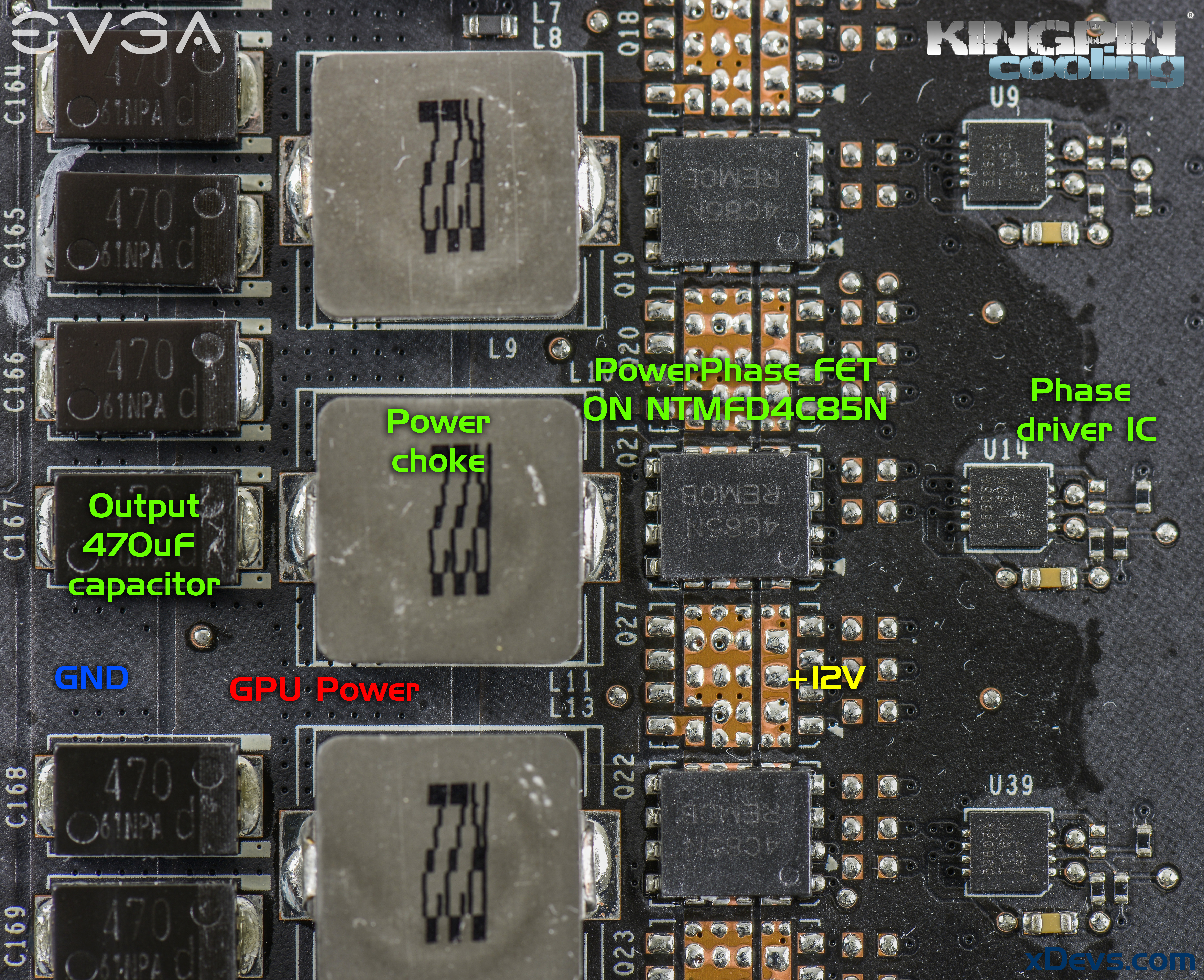
Image 26: Power circuits of GPU voltage regulator
PG413 reference design PCB have all six phases implemented for GPU power with two PowerPhase arrays on each phase, but currently only 5 are used for the GTX 1080 with only one PowerPhase Dual NFET/phase. This is done to cost-down manufacturing and keep better efficiency on low/medium loads. It’s common design compromise, as higher power regulators are also taking bit more power in parasitic losses when power consumption not pushed to higher limits.
STEP 5 – Memory voltage trim-pot mod
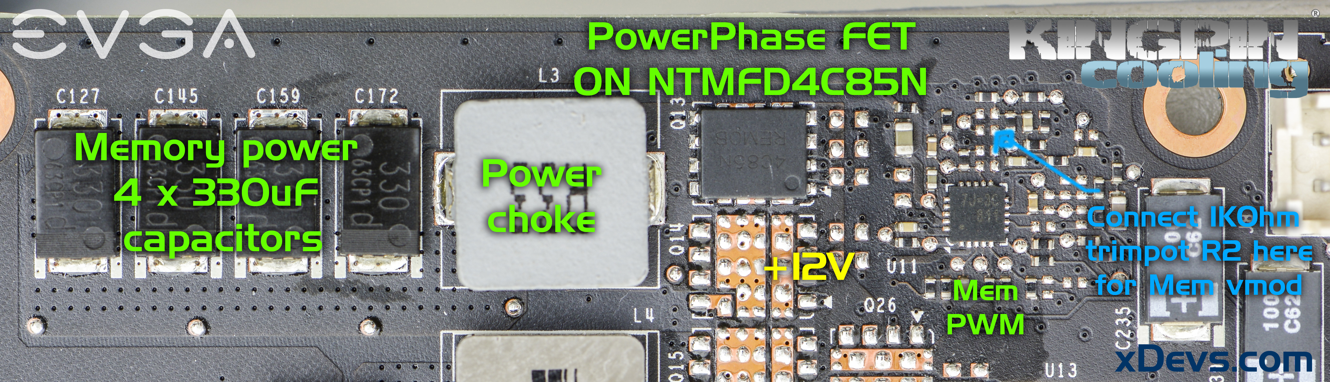
Image 27: Memory regulator and power parts
Memory VRM using single phase, with same 25A PowerPhase dual NFET and output fixed 1.35V for all eight GDDR5X memory chips.
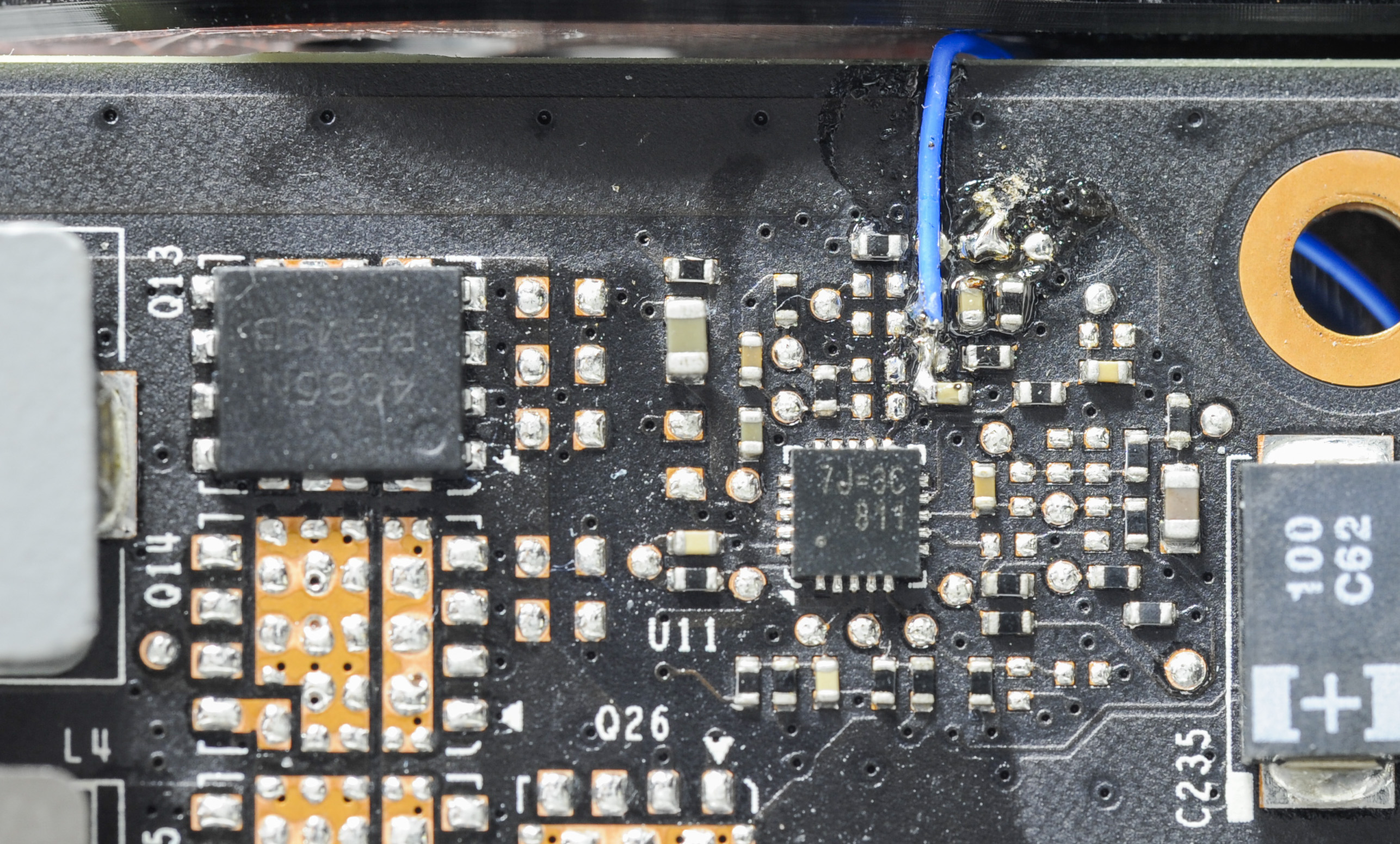
Image 28: Modified memory circuit to raise voltage
To raise voltage all you need to do is just 1KΩ trimmer to GND at marked point.
STEP 6 – PLL Voltage trim-pot mod

Image 29: PLL voltage regulator
PLL regulator is common and known from previous GPUs, so nothing new here. PWM chip used is uPI UP1628Q in tiny DFN package. Modification to raise voltage on it is straight forward and involve connection of 100KΩ trimmer to GND and point on the photo above.
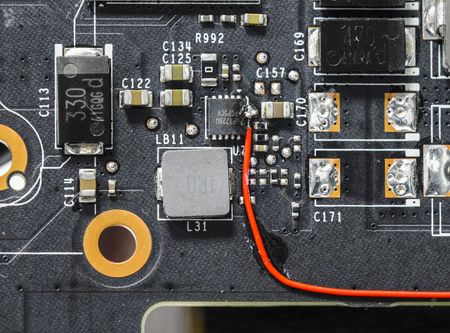
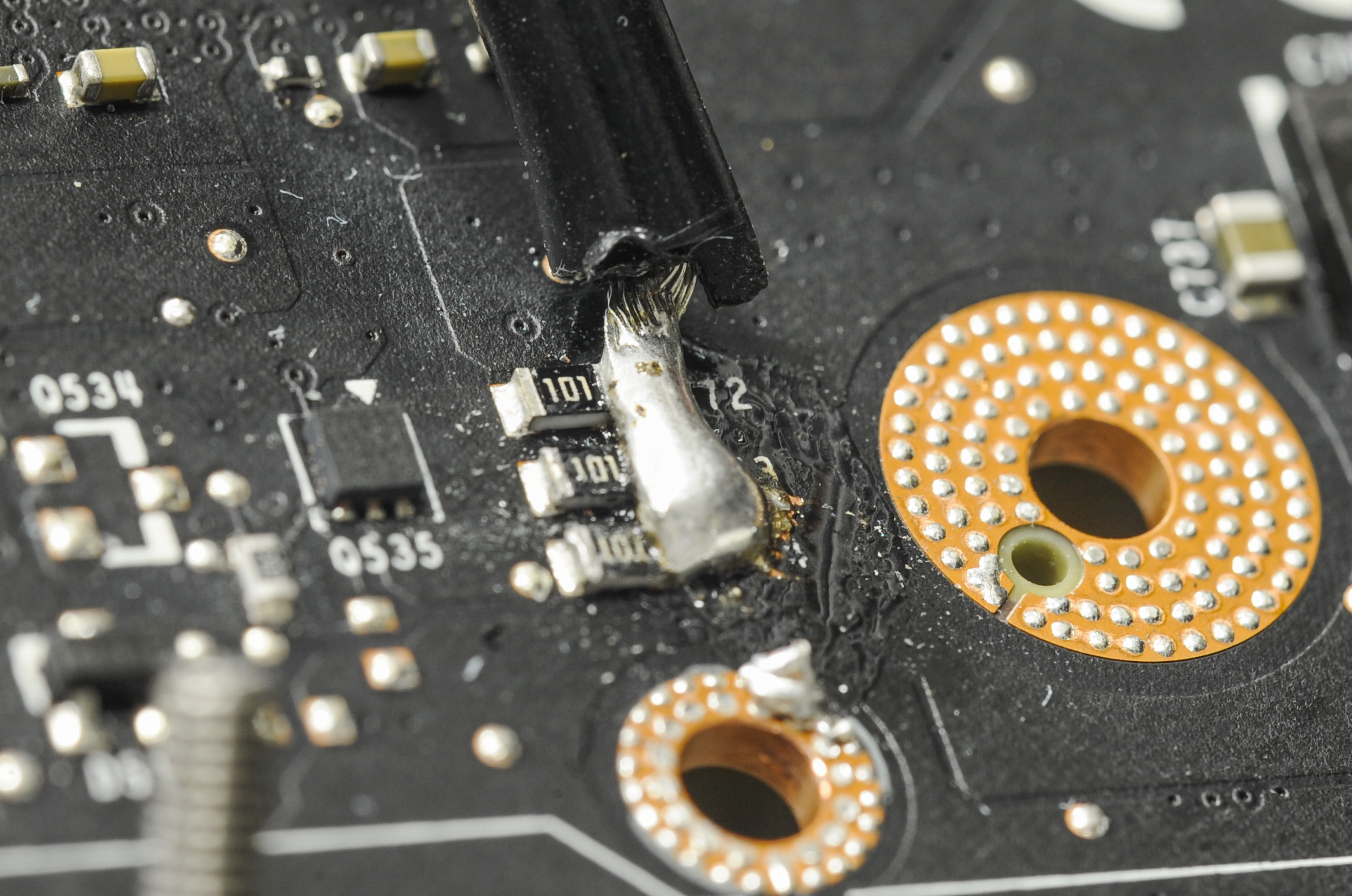
Image 30-31: Connected trimmer wire and monitoring point
Monitoring of PLL voltage output can be done by soldering wire to location of three resistors near bottom left GPU fan-sink mount hole.
STEP 7 – AUX Voltage trim-pot mod
GDDR5X memory need extra voltage rail, so now additional power supply regulator is used to provide 1.8VDC. It can be found right near power monitoring circuits on right side of PCB.

Image 32: Auxiliary 1.8V regulator location
1MΩ (1 mega Ohm = 1000000 Ohm) trimmer is required for this mod.
Too low resistance causes higher than 2V output and is dangerous for card. Make sure you start with small voltage increments and test each step well.
Resistor trim point to GND is shown below:
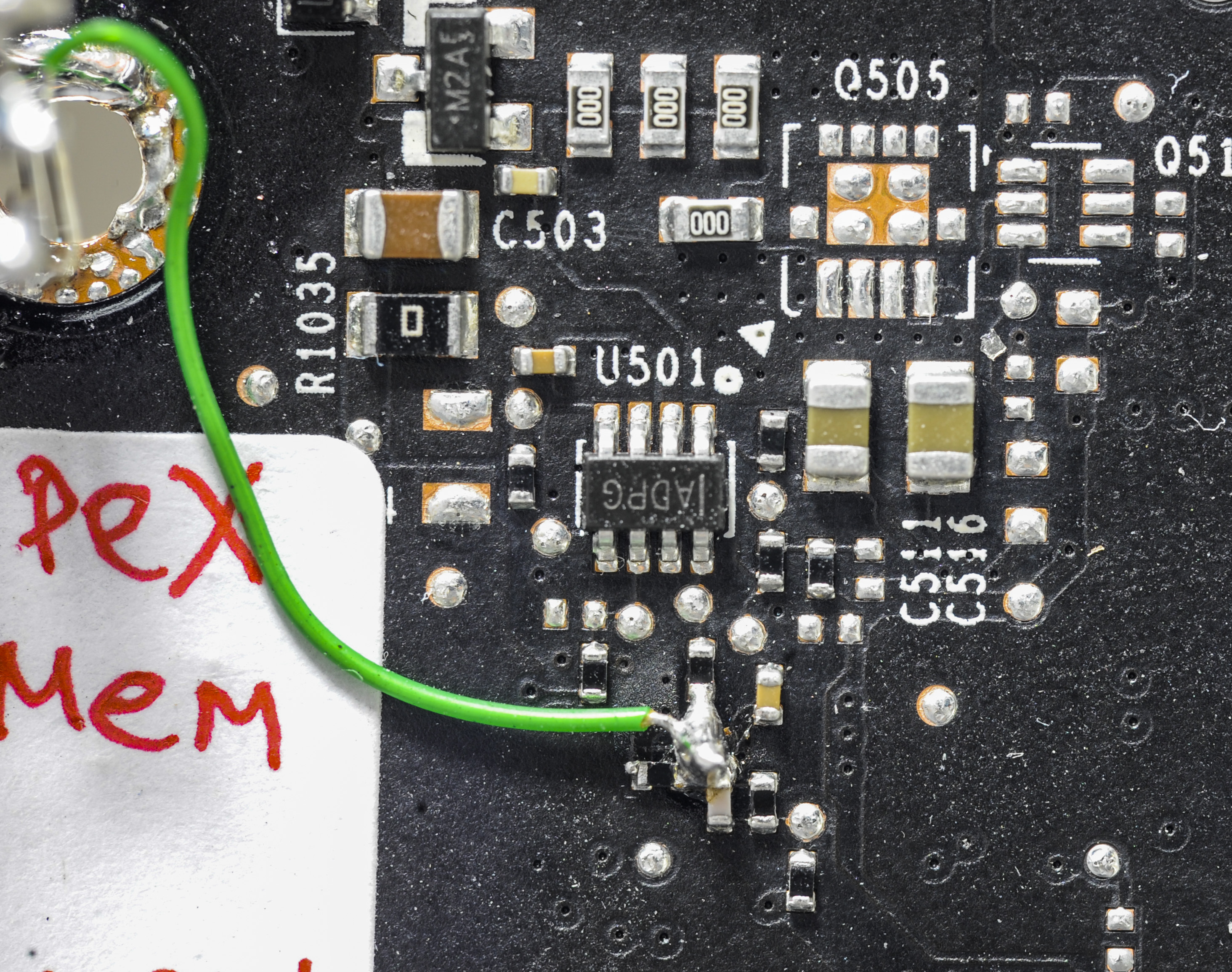
Image 33: Wire connection to increase 1.8V rail
This mod is not expected to improve overclocking on most of the cards.
Now everything is finally ready for some serious testing. Make sure you start with little voltage adjustments first and note all steps as you go higher and higher. This will help you to understand how voltages and things affect stability and make further overclocking easy.
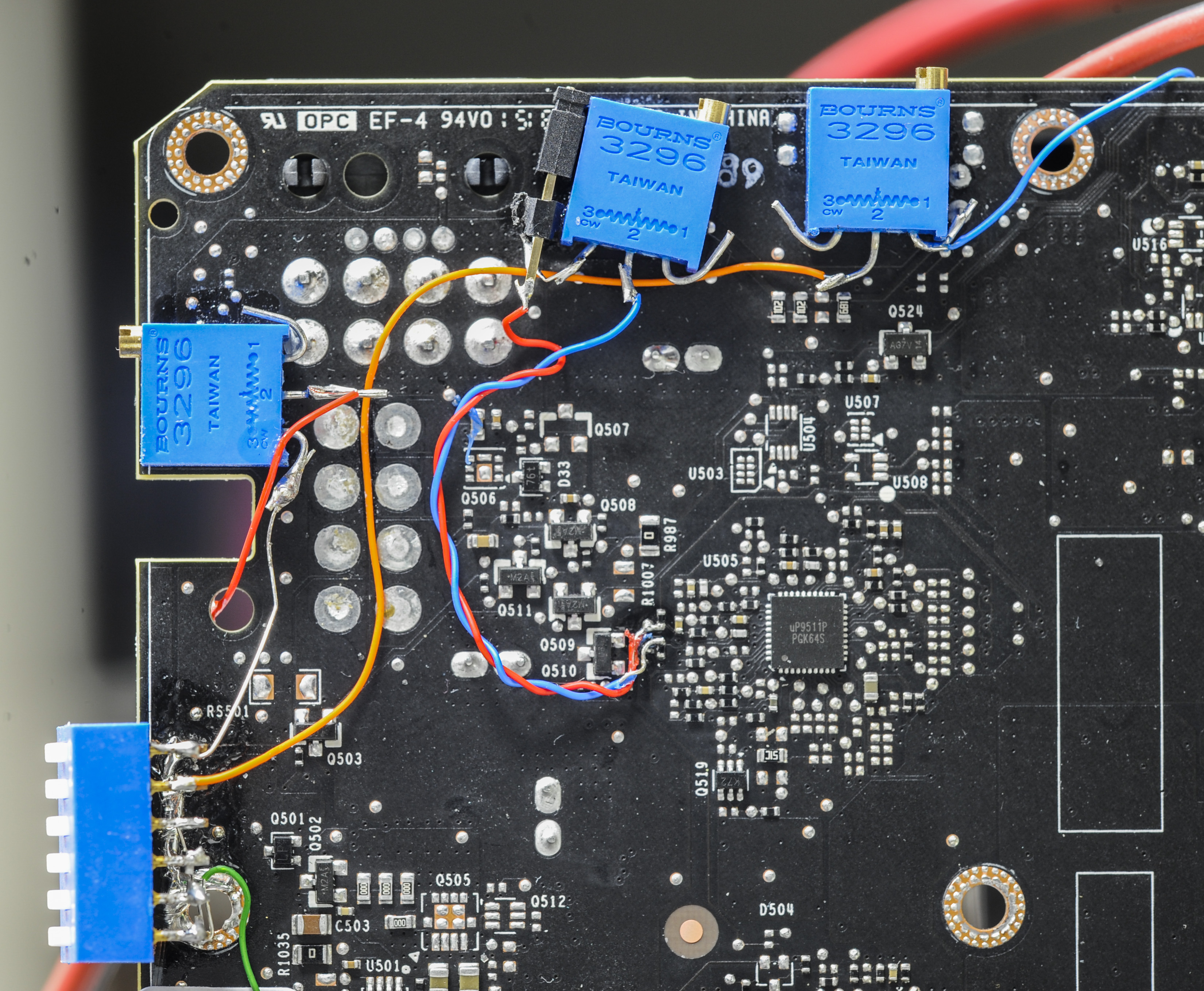
Image 34: All modifications in place
I also used DIP switch to get ability of turning off memory and PLL vmods ON/OFF in real-time, so actual impact of different voltages can be quickly tested during one bench session:
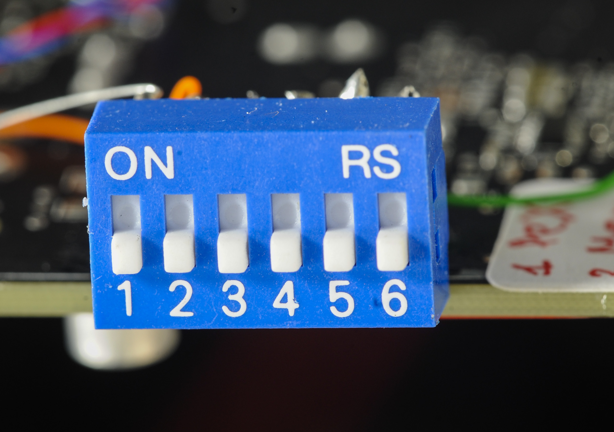
Image 35: DIP switch to turn mods ON/OFF
STEP 8 – Remove thermal protection
To avoid losing power doing LN2 overclocking when GPU temperature can reach below -50°C, remove D505 component, located on the bottom side of the board near the GPU power controller area.
Warning! This modification essentially removes thermal protection mechanism, and in case of overheating GPU will be permanently damaged. Always make sure your cooling solution is installed correctly.
STEP X – BONUS

Image 36: Reflection of GPU on Kingpincooling TEK9 FAT
Extreme overclockers often like to put some brutal bodges over their cards, so here are locations to add more capacitors:
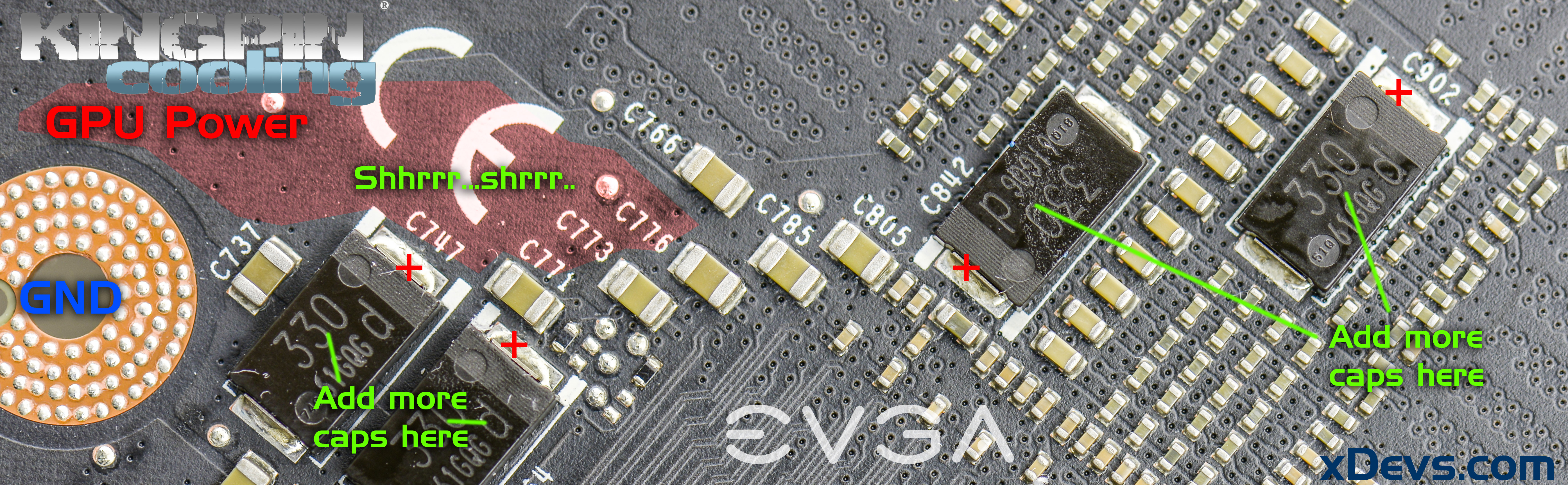
Image 37: Best locations for additional capacitors
Note that those red marks are not X but “plus” to show you location of positive voltage terminal. Electrolytic and tantalum capacitors are POLAR devices and must be soldered in proper polarity, positive to positive, and negative to negative. Or big fireball and unrepairable damage can occur to your hardware.
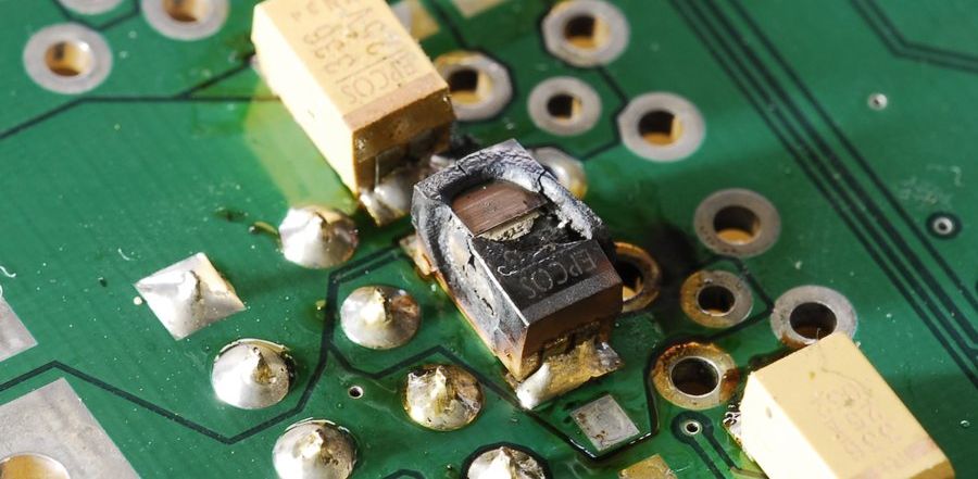
Image 38: Do not solder polar capacitors in wrong polarity!
Extra capacitors may or may not help to push higher clocks. Up to you to find out that.
For die-hard EPOWER guys, here’s magic sauce to enable EPOWER function on this cards. If you got reading to this section, you should already know how to use EPOWER, how to connect it to graphics cards and all the usual stuff.
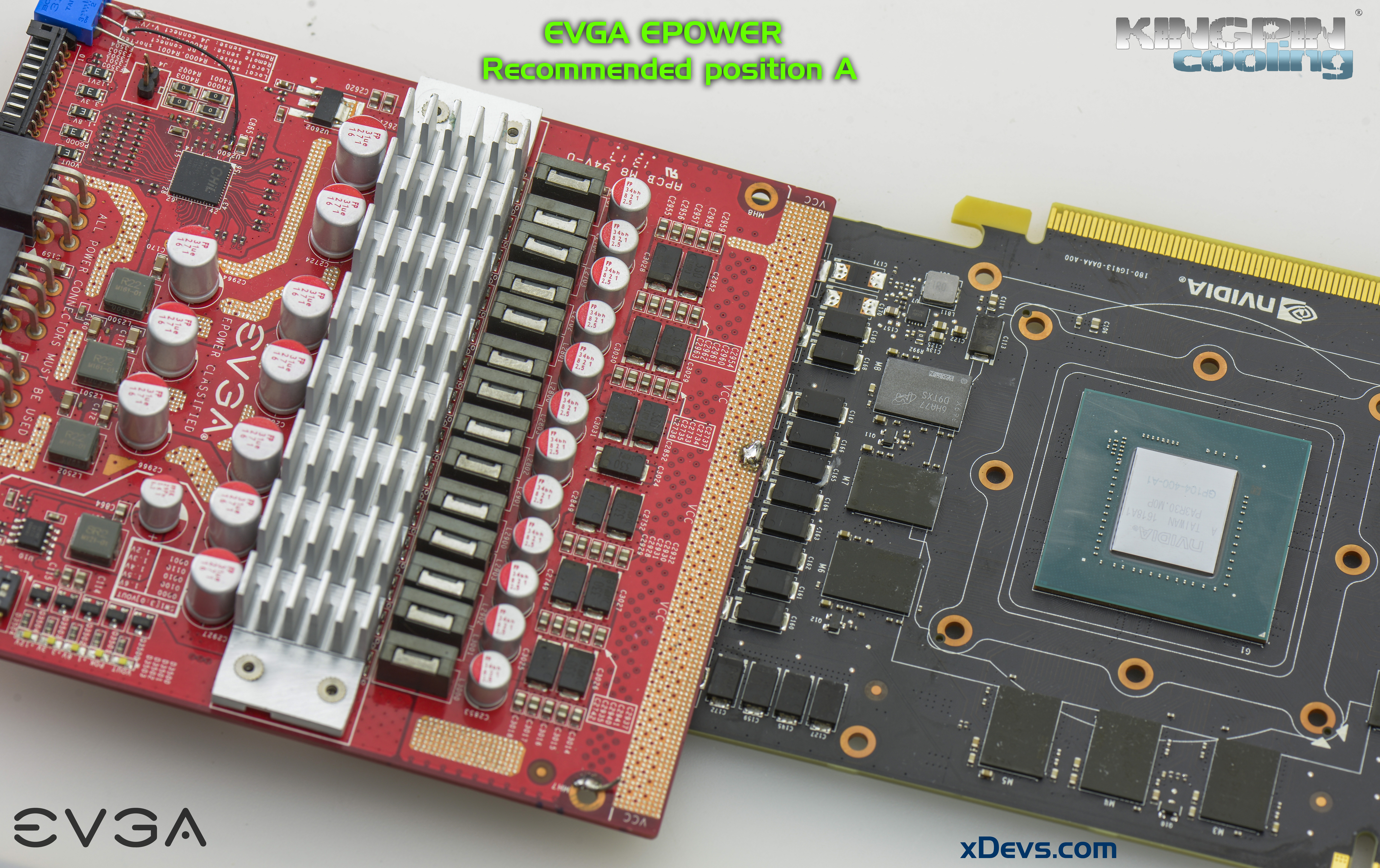
Image 39: Option A with EPOWER on the front
There are two possible positions for best EPOWER connection. Option A is best in terms of power delivery, but might be bit tricky to solder on and need to be more careful doing shhrrr-shhhrr on power copper plane. Usual “remove 5 inductors”, shhrr-shhhrr PCB solder mask (black paint) to get more copper for connection, soldering copper bars apply here. Applying EPOWER was covered in great detail in previous 980Ti reference mod guide. Be sure to check it out.
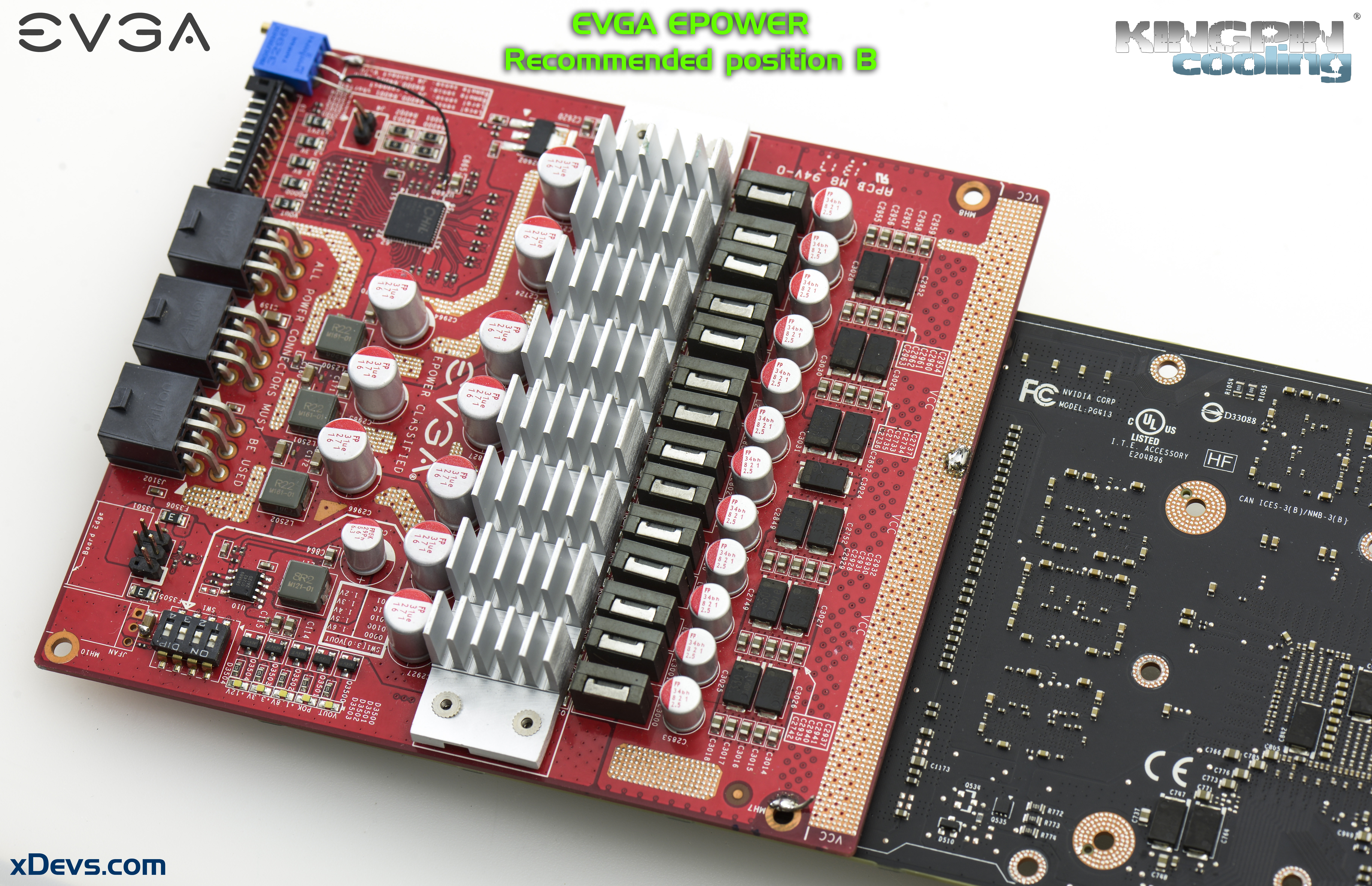
Image 40: Option B with EPOWER on the back
Option B is at the card’s bottom side, where you can easily connect VCORE output from EPOWER to card’s GPU power plane near long array of ceramic capacitors. Second side is one nice ground, plane, so that can be shhrr-shhrr’d to get robust GND connection.
Some shhrrr-shhrrr areas for better understanding:
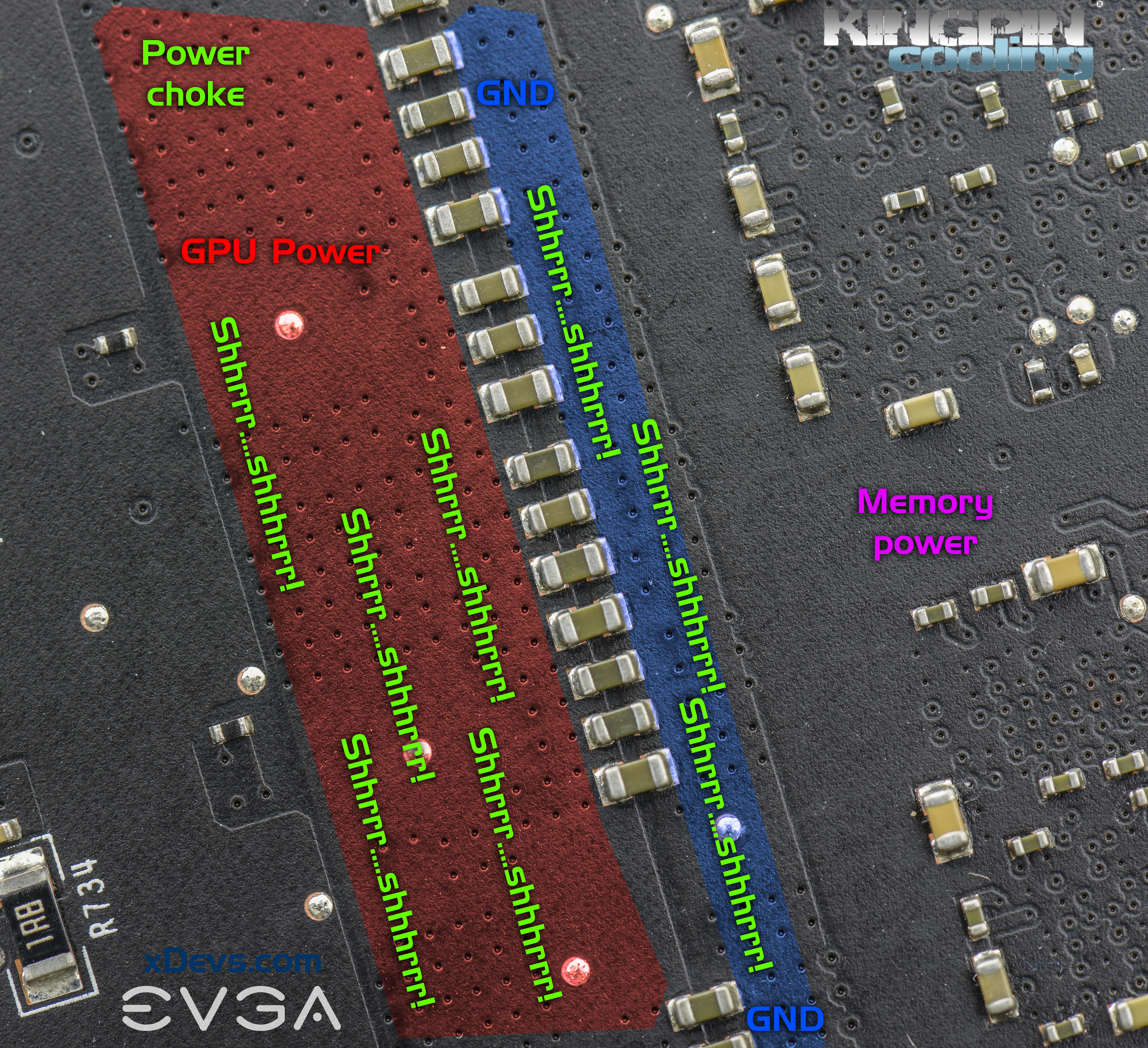
Image 41: Areas to remove black solder mask paint for better copper connections
Check again, if everything good, no shorts on the card or damaged parts, solder blobs or dirt. Make sure all trimpots are set to proper value.
Assemble your cooling solution to a card, test voltages and give it a spin on overclocking, using EVGA Precision XOC 16.
Since you unlikely to get EVBOT today, one of the ways is to reuse Raspberry Pi to control voltage. It’s fairly simple and well explained before.
Secret mod for EPOWER. Cut trace marked red on photo below. Make sure not to cut anything else  .
.
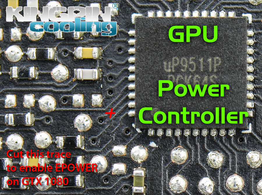
Image 42: Cut trace to enable EPOWER operation with GTX 1080
Also here are reference points, key resistance values measured with high-accuracy Keithley 2002 DMM on good working card:
| Voltage rail | Resistance measured | Nominal voltage |
| NVVDD | 80-250 milliΩ | 0.64 VDC … 1.21VDC |
| FBVDD | ~97 Ω | 1.35 VDC fixed |
| PEX | ~44 Ω | 1.02 VDC fixed |
| MEMPLL | ~450 Ω | 1.80 VDC fixed |
Table 1: Nominal resistance on main power rails from good GeForce GTX 1080 card
If you get very different resistance readings, you card is likely borked and game is over.
Voltage scaling and “1.25V limit”
There were some rumors spreading wildly these days regarding “1.25V limitation” or whatever on modified GTX 1080 cards, which requires here few words to explain.
Hardware itself is well capable of getting to that and above voltage output for GPU core, but GP104 chip itself now more sensitive to voltage, than even previous Maxwell generation. Part of it due to thinner physical process, other part due to challenges removing heat from all those tightly packed 7.2B transistors quick enough from 21% less surface area. Those overclockers who did 2200+ MHz on GTX 980 Ti’s are well aware of all things required to achieve those high clocks. Same principle applies to Pascal generation. So if you can manage to keep GPU cooled well and have good voltage delivery to it, you indeed can push higher voltages. Cards cooled by liquid nitrogen during this guide testwork were able to run 1.35-1.4V, reaching speeds over 2500 MHz.
Fact that GTX 1080’s capable of reaching 2.1GHz on aircooling without any modifications confuse lot of people, making them to think that these chips can overclock well past 3GHz on liquid nitrogen cooling. But it’s still silicon, with similar architecture, so reality is bit sour. Yes, it allow to get good performance without extreme cooling, but hides the fact that LN2-cooled 980Ti is still much faster than overclocked GTX 1080 due to more shader cores and better CPC performance.
This also brings and answer to the question if overvolting can help OC on aircooling or watercooling. It does not help, due to thermal, which get only worse. Higher temperature render stability and performance decrease. GPU literally overheats and cannot run high frequency anymore, even though temperature is below specified maximum temperature +94°C. Think of it as temperature to frequency dependency, all the way down from +94°C to -196°C, with slope around 100MHz every 50°C. So just like in 980/980Ti/TitanX case, over-voltage on aircooling/watercooling is not recommended, as it gains little if any performance improvement.
Don’t get this message wrong, as GTX 1080/1070 are still great cards for daily gaming/content creation and VR experience. They are fast, not power hungry, moderately cool. The only catch is that overclocking them is not as fun and rewarding as it was on previous generations, even considering all tricks involved to get Maxwell clock high.
As usual, any feedback and questions are appreciated. Feel free to share link to this guide, but keep links and references intact, as guide likely to be updated in future.
Modified: Aug. 4, 2017, 1:25 p.m.
References
- Using Raspberry Pi to control your VGA VRM
- Removing power limits on any NV card
- EVGA GTX 980 Ti K|NGP|N OC Guide
- Reference GTX 780/780Ti - Big KEPLER
- EVGA GTX 680 Classified - Uncorking guide
- Reference GTX 680 - Uncorking KEPLER
- Review of ERSA I-CON Soldering station
- NVIDIA GeForce GTX 1080 : Whitepaper PDF