- Intro
- Disclaimer
- Manuals and service information
- Exterior
- Design and internal design review
- Firmware
- Battery installation and initial checks
- Performance testing
- Experiment 1: Board surface leakage
- Experiment 2: Capacitor leakage
- Conclusion and summary
Introduction
Picoammeter is an electrical instrument able to detect and accurately measure extremely low currents. Modern instruments of this type based on state of the art solid state devices can be used to measure currents down to femtoamperes (10-15 A or 15 zeroes after decimal point). To give some perspective how small these currents are, compare current 1 Amp (typical charging current for devices we use every day, like smartphone) with length unit of distance – 1 meter. Scaling down to femtometer scale bring us to realm of elementary particle sizes, where neutron-proton nuclei (not atom itself!) of Hydrogen have radius about 1.8 femtometers.
The electrometer can measure electric charge or electrical potential difference. Simplified way is to understand electrometer as special version of traditional voltmeter/ammeter. Electrometer can be used for many measurement tasks, just like regular DMM but also offering the advantage of ultra-high input resistance when used as voltmeter or ultra-sensitive current measurement with low voltage burden when used as ammeter.
As result these instruments can do things that none of bench-top DMMs able to reach, like measuring circuits that cannot support loading caused by DMM input. That makes electrometers the go to choice for measuring weak signals and voltages with high source impedance or low currents with low source impedance. Electrometers can also measure charge and provide direct reading in coulombs. They are often used in research, detector and sensor validation and analysis, photonics applications, semiconductor characterization, dielectrics and material properties measurements.
Keysight Technologies B2980A series include four benchtop instruments, from basic high-performance picoammeters (B2981A and B2983A) to fully featured electrometer equipped with integrated high-voltage source and high-impledance voltage input (B2985A and B2987A). In this article we will take a look on top SKU – Model B2987A Electrometer/High-resistance meter.
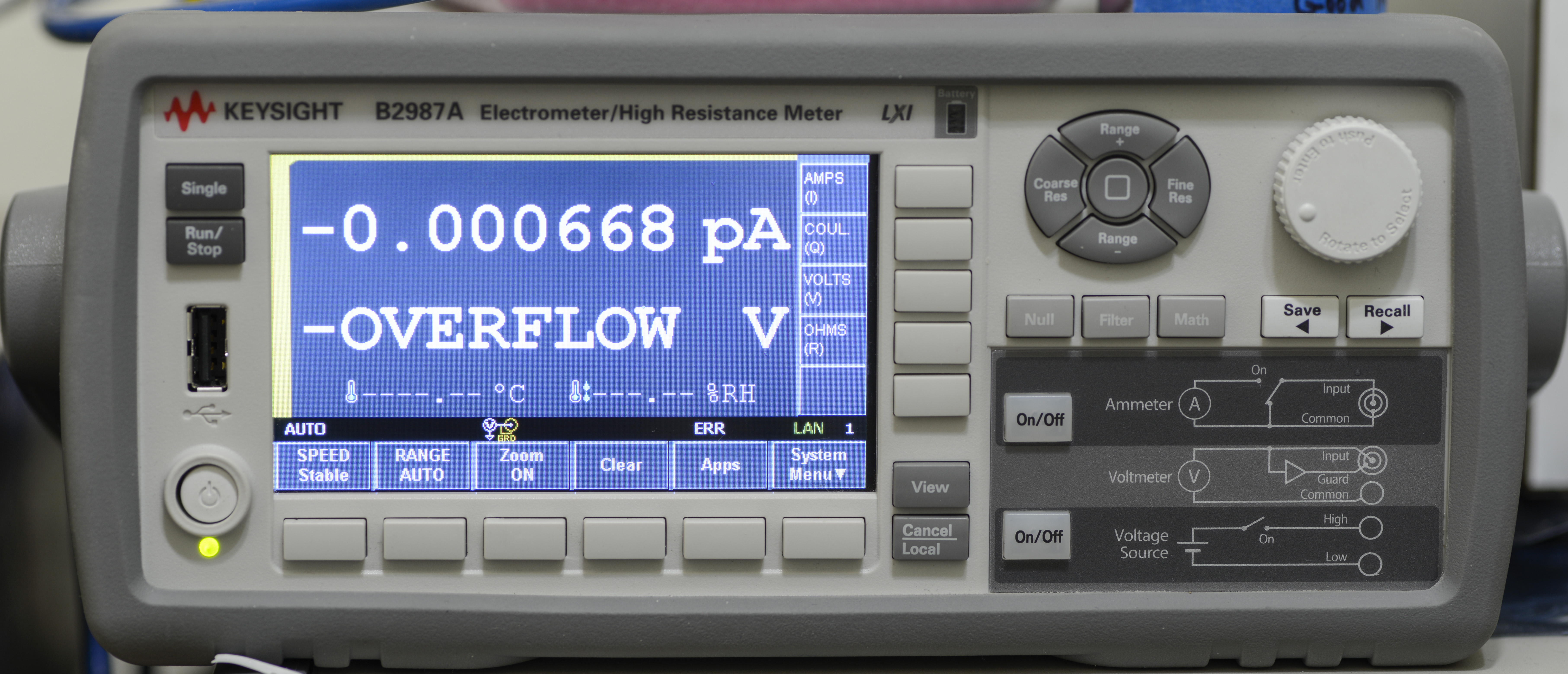
Image 1: Keysight B2987A front face
To understand why high impedance of the voltmeter can be important, we can try to compare portable DMM and high-end DMM with electrometer, in role of the voltage measurement device. As a device under test we pick some high-impedance output source, such as light sensor or humidity sensor. For sake of this mind experiment we picked Zsource = 100 MΩ.
| Parameter | Typical portable DMM | High performance DMM, like Keysight 3458A | Keysight B2987A electrometer |
|---|---|---|---|
| Measured DUT output source impedance | 100 MΩ | ||
| DMM annual 10V range accuracy specification | ±0.05 % | ± 8 ppm (0.0008%) | ± 250 ppm (0.025%) |
| DMM input bias current | <100 nA (typical) | <20 pA (typical) | <20 fA (typical) |
| Voltmeter input impedance | 10 MΩ (typical) | 10 GΩ (typical) | 200 TΩ (typical) |
| Measured reading error due to DMM loading | 90.9% | 1 % | 0.00005 % |
| Total error | useless | 1% due to loading + DMM spec = 1.0008% | 0.0001% due to loading + Vmeas spec = 0.025% |
Table 1: High-impedance voltage source measurement comparison between different type voltmeters
Values above are NOT complete accuracy specifications and not include all error contributors of the measurement setup, but give the basic idea how DUT loading with meters own input impedance can affect the measurement results.
Similar situation also possible for current measurement function, when low voltage burden feature of electrometer is important. Voltage burden is the voltage that appears across the ammeter input terminals, when ammeter is placed in the DUT circuit.
Nearly all DMM use a precision shunt at the current input terminals. Shunt require few hundred millivolts voltage signal to be developed across in order to convert current flowing thru shunt into ADC input voltage to calculate the current. This undesired voltage drop or voltage burden for the DUT circuit as result reduce the actual current flowing in the load and reduce measurement accuracy. Voltage seen by DUT device after the shunt-based ammeter also would be equal to Vsource – Vburden. If DUT is sensitive to input voltage change, it may malfunction or have incorrect operation, even making measurement result invalid.
Electrometer’s ammeter circuit uses a feedback-type circuit to reduce this terminal burden voltage by multiple orders of magnitude. Modern electrometers also can go a step further, actually sourcing additional compensating voltage that eliminates any residual offset voltages at the ammeter input, further reducing burden down to as little as 20µV. This way you can measure wide range of currents with near zero effect the measured circuit.
| Functionality | Keysight B2981A | Keysight B2983A | Keysight B2985A | Keysight B2987A |
|---|---|---|---|---|
| Current measure | 0.01 fA to 20 mA, 6½ resolution | |||
| Voltage measure | Not available | up to 20 V | ||
| Voltage source | Not available | programmable, up to ±1050 VDC | ||
| Charge measure | Not available | 1 fC to 2 µC | ||
| Resistance measure | Not available | up to 10 PΩ (Petaohm) | ||
| Battery option support | No | Yes | No | Yes |
Table 2: Keysight B2980A series instrument variants
Disclaimer
Redistribution and use of this article, any part of it or any images or files referenced in it, in source and binary forms, with or without modification, are permitted provided that the following conditions are met:
- Redistributions of article must retain the above copyright notice, this list of conditions, link to this page (https://xdevs.com/article/b2987a/) and the following disclaimer.
- Redistributions of files in binary form must reproduce the above copyright notice, this list of conditions, link to this page (https://xdevs.com/article/b2987a/), and the following disclaimer in the documentation and/or other materials provided with the distribution, for example Readme file.
All information posted here is hosted just for education purposes and provided AS IS. In no event shall the author, xDevs.com site, or any other 3rd party, including Keysight Technologies be liable for any special, direct, indirect, or consequential damages or any damages whatsoever resulting from loss of use, data or profits, whether in an action of contract, negligence or other tortuous action, arising out of or in connection with the use or performance of information published here.
If you willing to contribute or add your experience regarding instrument repairs or provide extra information, you can do so following these simple instructions.
Manuals references
B2980A User’s Guide, Edition 4, March 2016
B2980A Programming Guide, Edition 2, March 2016
B2980A SCPI Command Reference, Edition 3, March 2016
To our misfortune there are no service or calibration manuals available for any of the B2980A series instruments.
AN: Reliable High-Resistance Measurements Using the B2985A/87A
AN: Low Current Semiconductor Measurements Using the B2980A Series Ammeter
AN: Measuring Insulating Material Resistivity Using the B2985A/87A and N1424
N1414A High Resistance Measurement Universal Adapter brief
N1420A Setup Integrity Checker Function brief
Ion Beam Current Measurement – Product Fact Sheet
AN: Wide Range of Resistance Measurement Solutions from µΩ to PΩ
AN: Capacitance Leakage Current Measurement Techniques Using the B2985A/87A
AN: Real-time Noise Monitor Function in B2980A
N1424, N1425, N1427, N1428 Accessories for Keysight B2985A/B2987A
Keysight: Sensitive Measurement Considerations
Exterior
Instrument designed around common half-rack format, with large display and programmable front panel buttons. All inputs and connection ports are located on the instrument rear side. Optional battery is installed in the special bay located on the top side. Front and rear plastic bezel frame are protected from damage by rather massive rubber boots. Boots and adjustable handle can be easily removed for rackmount installation.
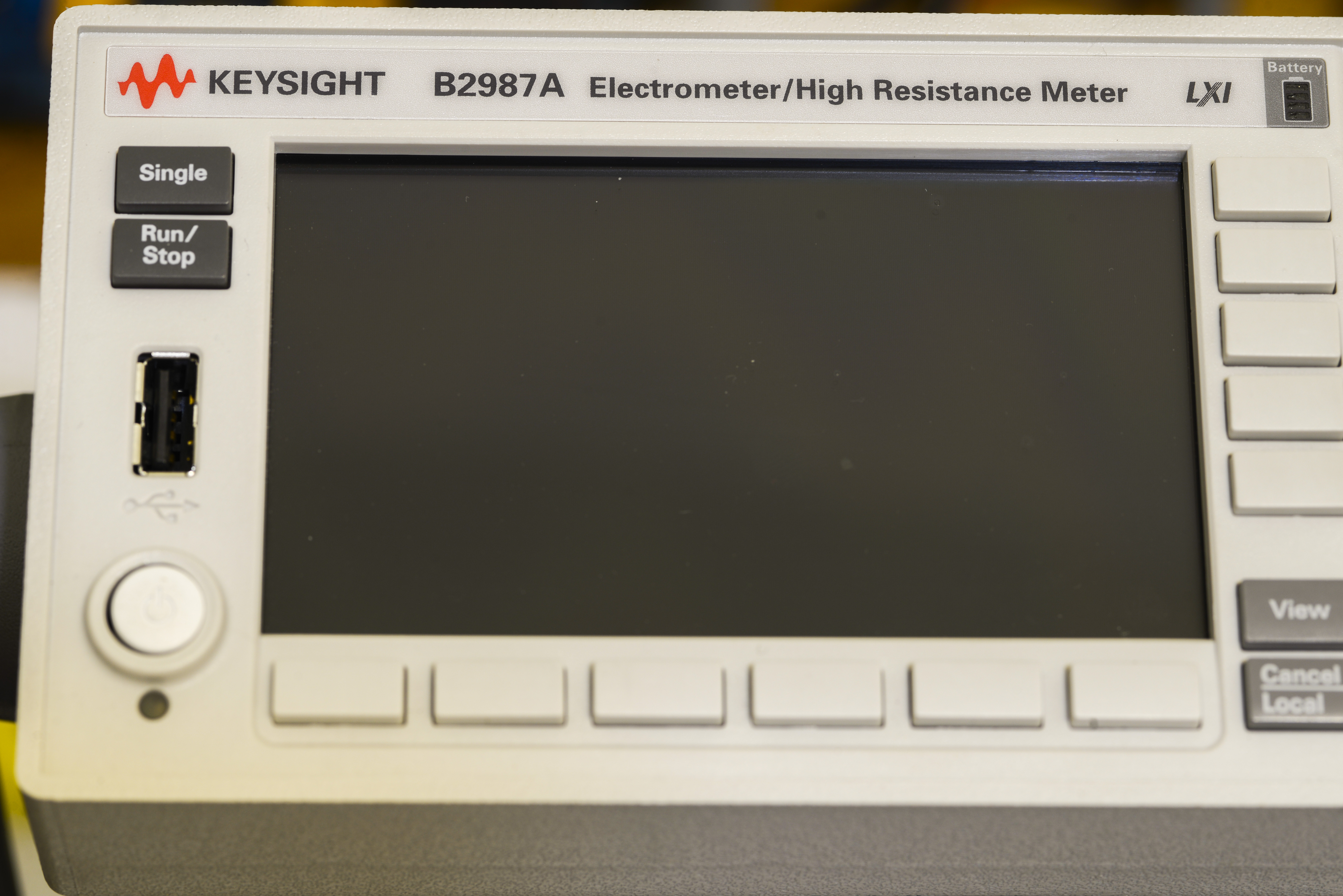
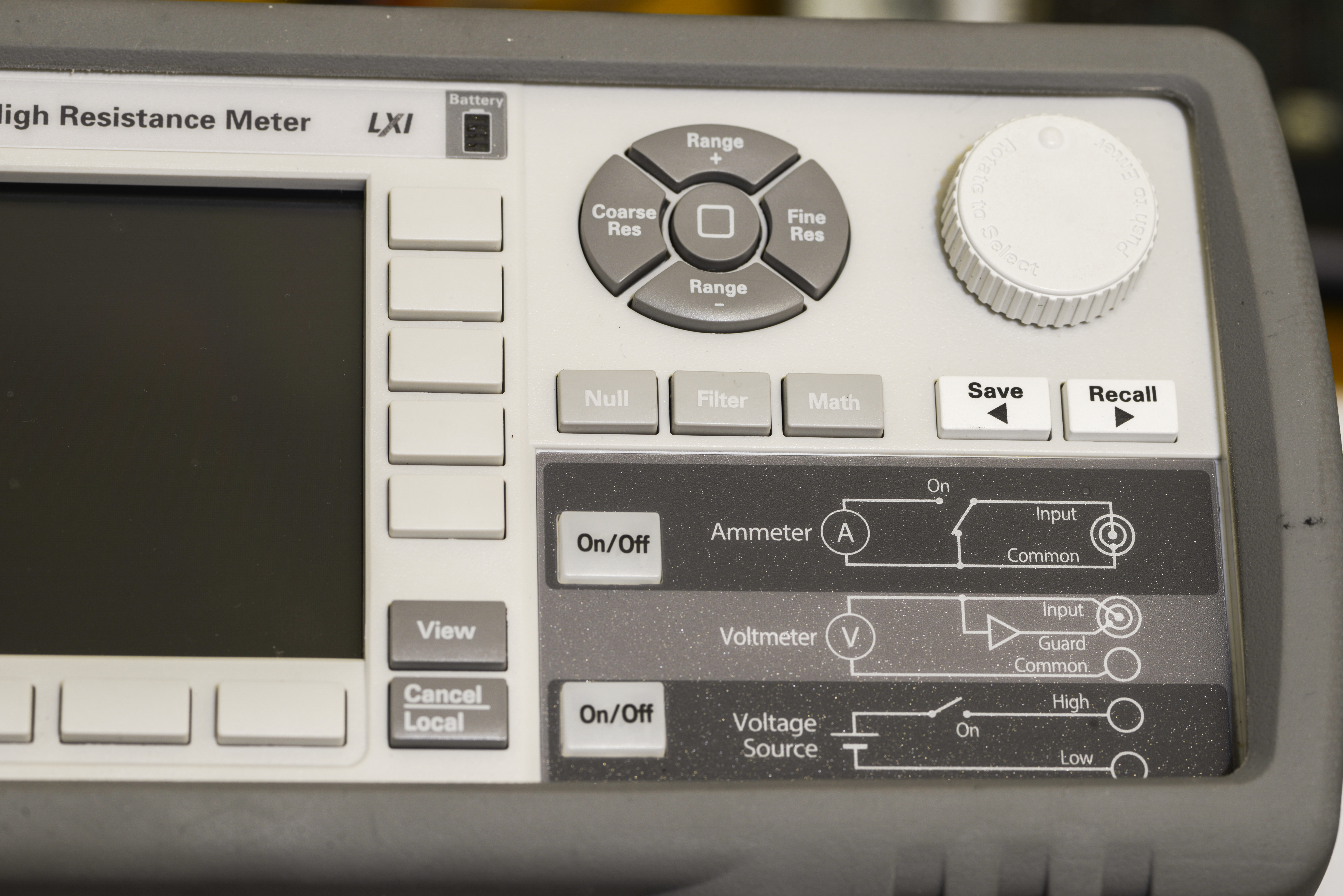
Image 2-3: B2987A front panel display and UI buttons
This electrometer is 100% silent, as it does not contain any fans. Fans generate vibration which can cause big problem for sensitive instrument like this. Vibration would translate into electrical noise by the triboelectric effects in cables and piezoelectric effects in ceramic-based components like surface-mount capacitors. The triboelectric charge is generated when friction stress applied to both cable conductor and insulator, resulting in charge stored on the insulator surface. This effect can be seen when vibration coupled into cable, and as a result, it is likely that there are many risks to suffer from this noise. Any cable on test setup and interconnect can act as the noise source due to triboelectrics.
So passive cooling design was important design constrain to meet. Generated heat managed by low-power electronics design and external enclosure cover extensive perforation to provide enough vent slots for better airflow. It is important to keep this in mind when installing the meter into tight spots or rackmount equipment setup.
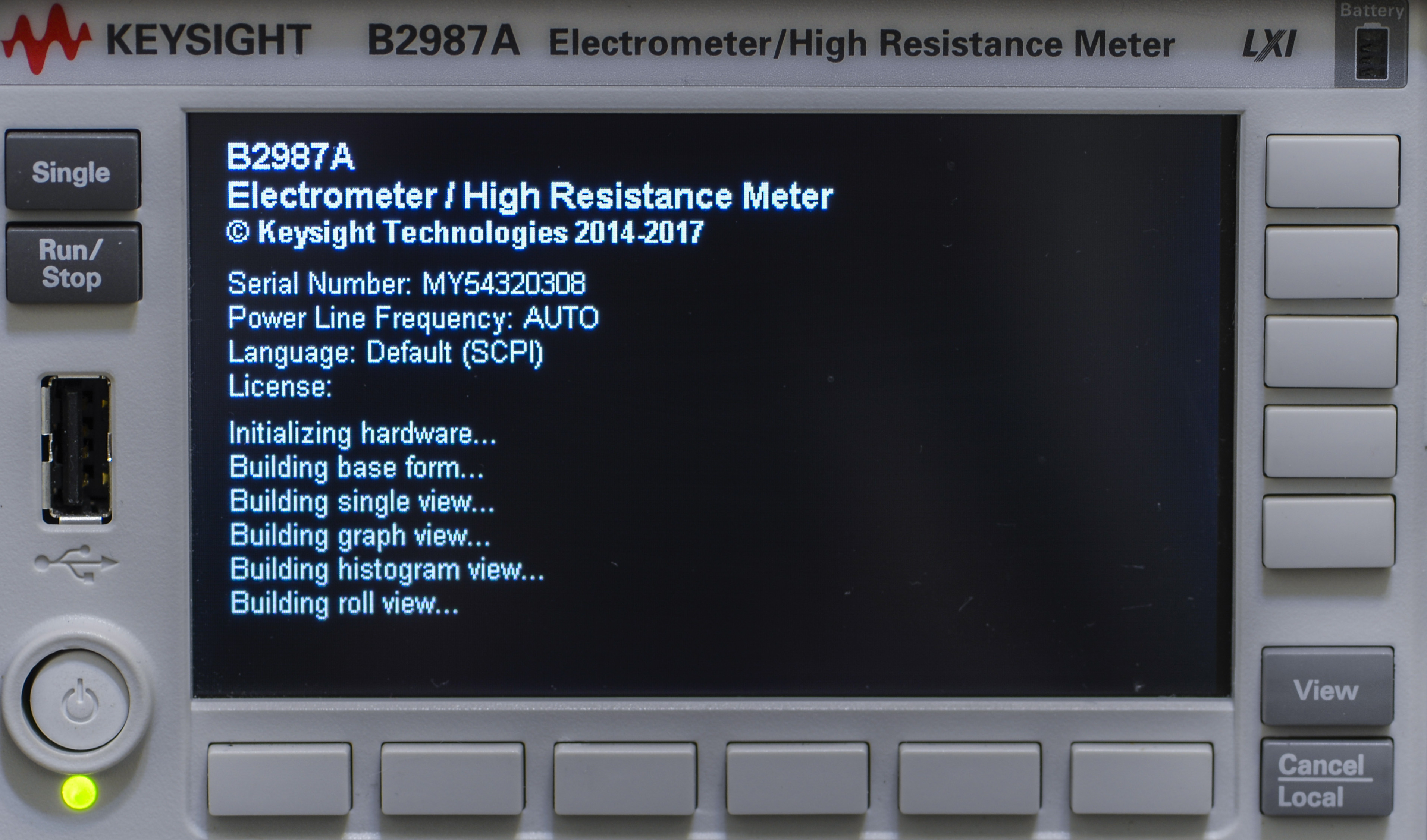
Image 4-5: Boot logo and start procedure information
Since this meter runs some sort of RTOS, it takes about 53 seconds to boot up before it’s ready for operation. It’s not important for typical workflow, as you need few hours warm-up time to reach specified accuracy but some engineers do like faster boot-up time for some reason.
Front panel sports full-color TFT panel without touchscreen, falling for modern trend with large LCD on everything, rather than expensive and fragile high-contrast VFD displays. Of course both display types have strong and weak spots, but contrast and visibility angles of the VFDs are not possible to beat with TFT panel. OLED provides great contrast too, but many of them fall by low life period. It is not uncommon for expensive test equipment to be in use for decades without powering off, so display life is one of the parameters to consider.
Also fonts used on display… Our apologies to Keysight engineers, but meter have at least five different fonts used in UI as they were not sure which one looks better. Why, Keysight?
Courier New font is not the best font for relatively small LCD display. Modern Keithley LCD GUI design in that respect much more pleasing, even though overall colorful TFT LCD displays in professional instruments more of a gimmick, than necessary functionality. Also LCD do always come out ugly on photographs, just a reviewer note.
Overall UI performance is rather underwhelming, it does not take lot of time to notice lags and lot of interface quirks during standard operation from front panel. Yes, yes, this instrument supposed to be put in the rack, connected over GPIB/LXI and never seen again, but it’s fair to expect wee bit more effort put into $11000 instrument..
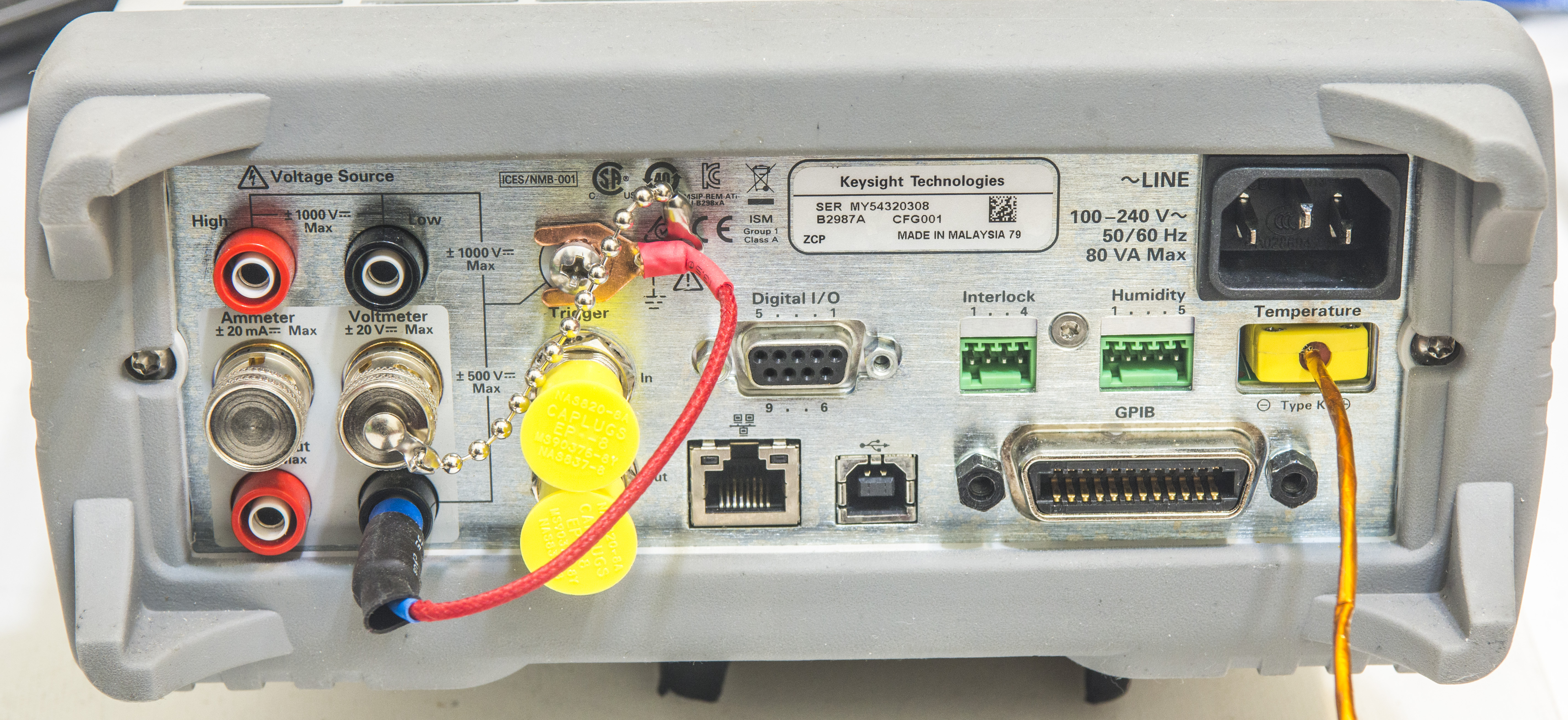
Image 6: Rear input connectors
Rear panel have lot of various interfaces and connectors:
- Voltage source HI/LO shrouded 4mm banana ports
- Analog output HI/LO shrouded 4mm banana ports
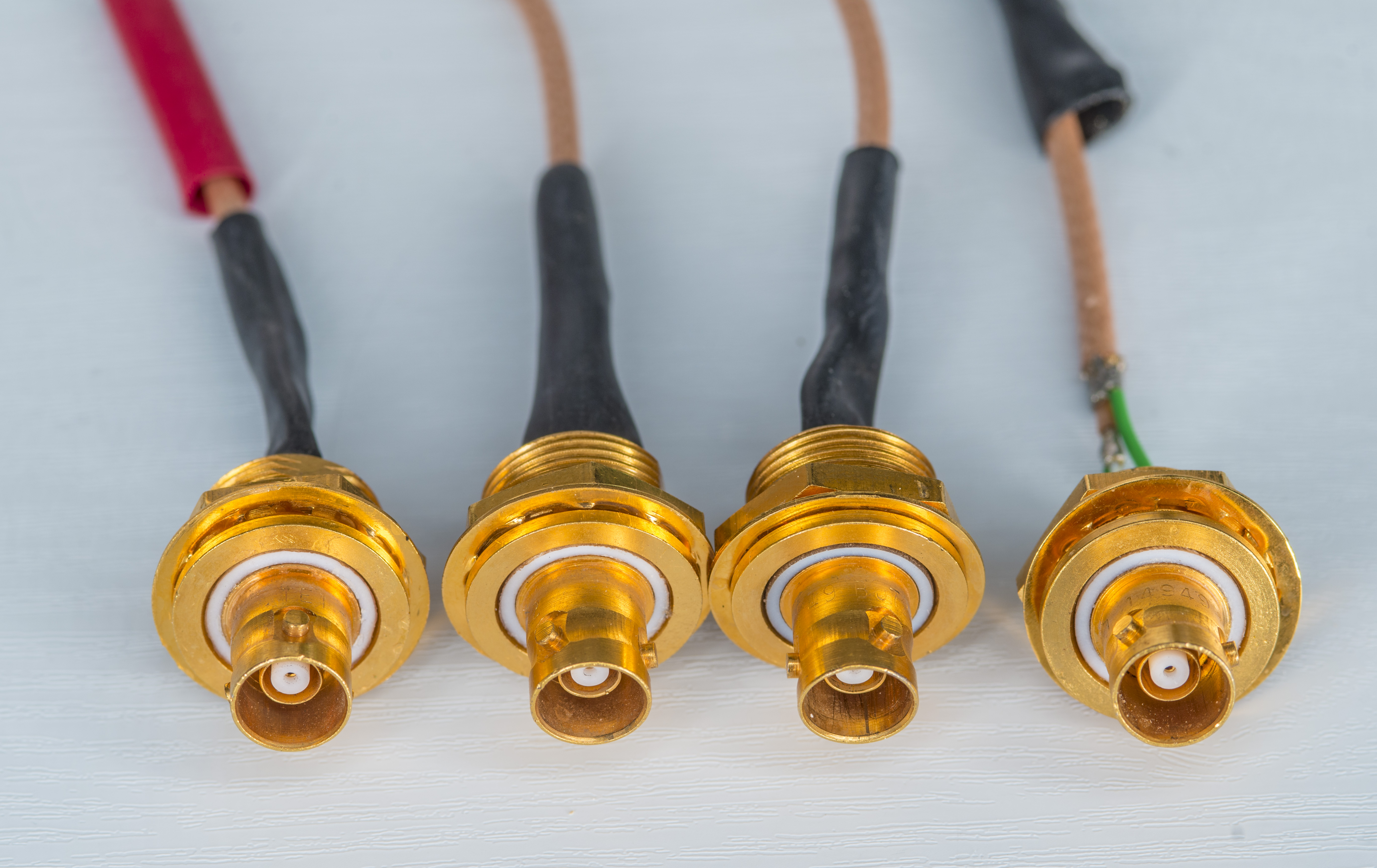
- Ammeter gold-plated 3-lug triaxial input (2 pA to 20 mA ranges)
- Voltmeter gold-plated 3-lug triaxial input (2 and 20V ranges)
- GPIB remote control port
- USB Device remote control port
- LAN remote control port with LXI support
- Trigger In and Out BNC ports for precise timing
- Digital I/O to interface DUT fixtures
- Interlock input for DUT fixture, to safely limit voltage source below 21V during DUT replacements
- Humidity digital interface port, designed to support E+E EE07 probe
- Type-K miniature thermocouple input with CJC sense
- Common point for chassis connection
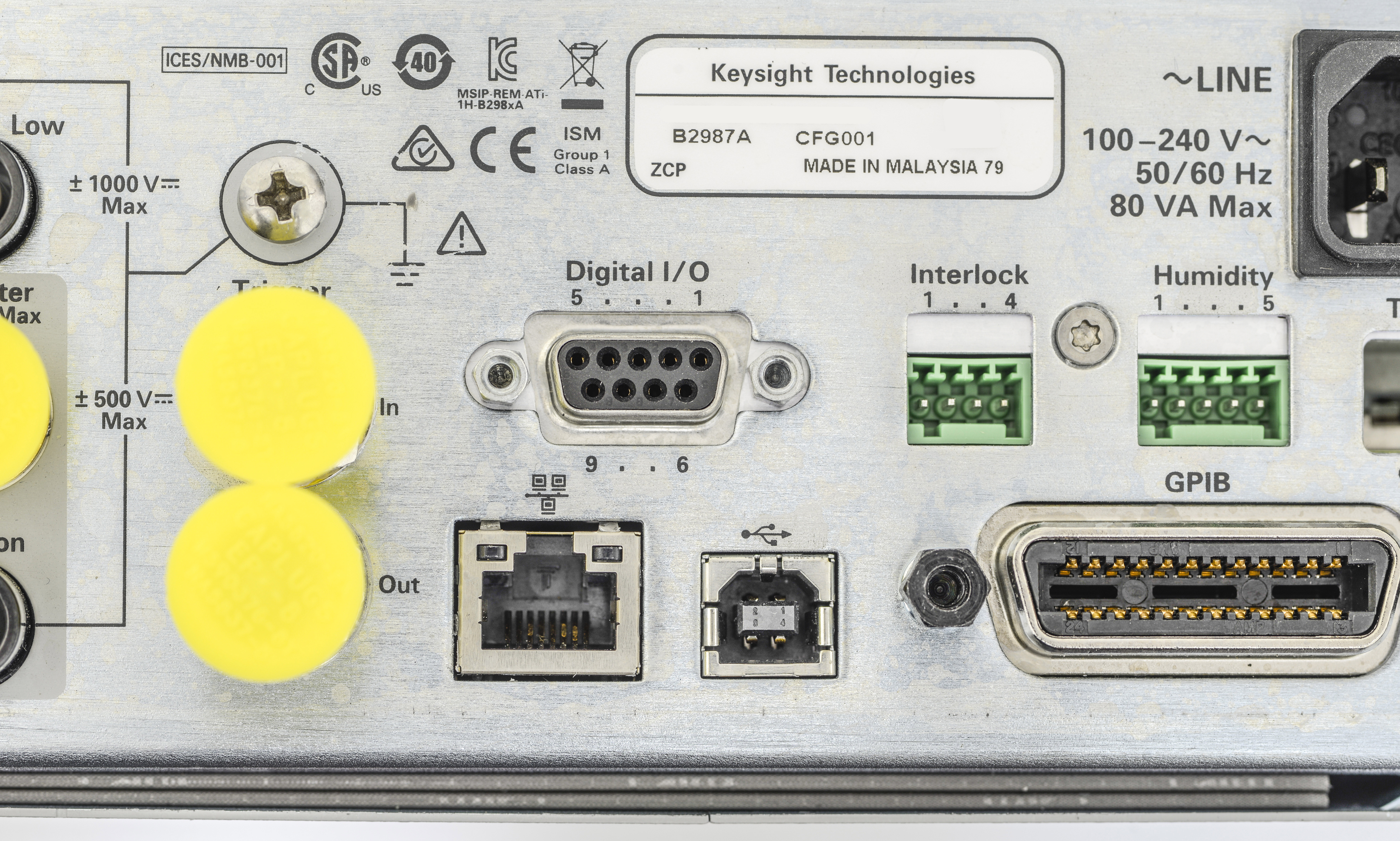
Image 7: Rear panel communication interfaces
Those triaxial inputs look so pretty with surface gold plating. We also see trigger BNC ports to allow syncronisation of the meter with another experiment equipment for precise timing. Also glad to see GPIB is still present on this modern instruments to allow easy integration within older instrumentation.
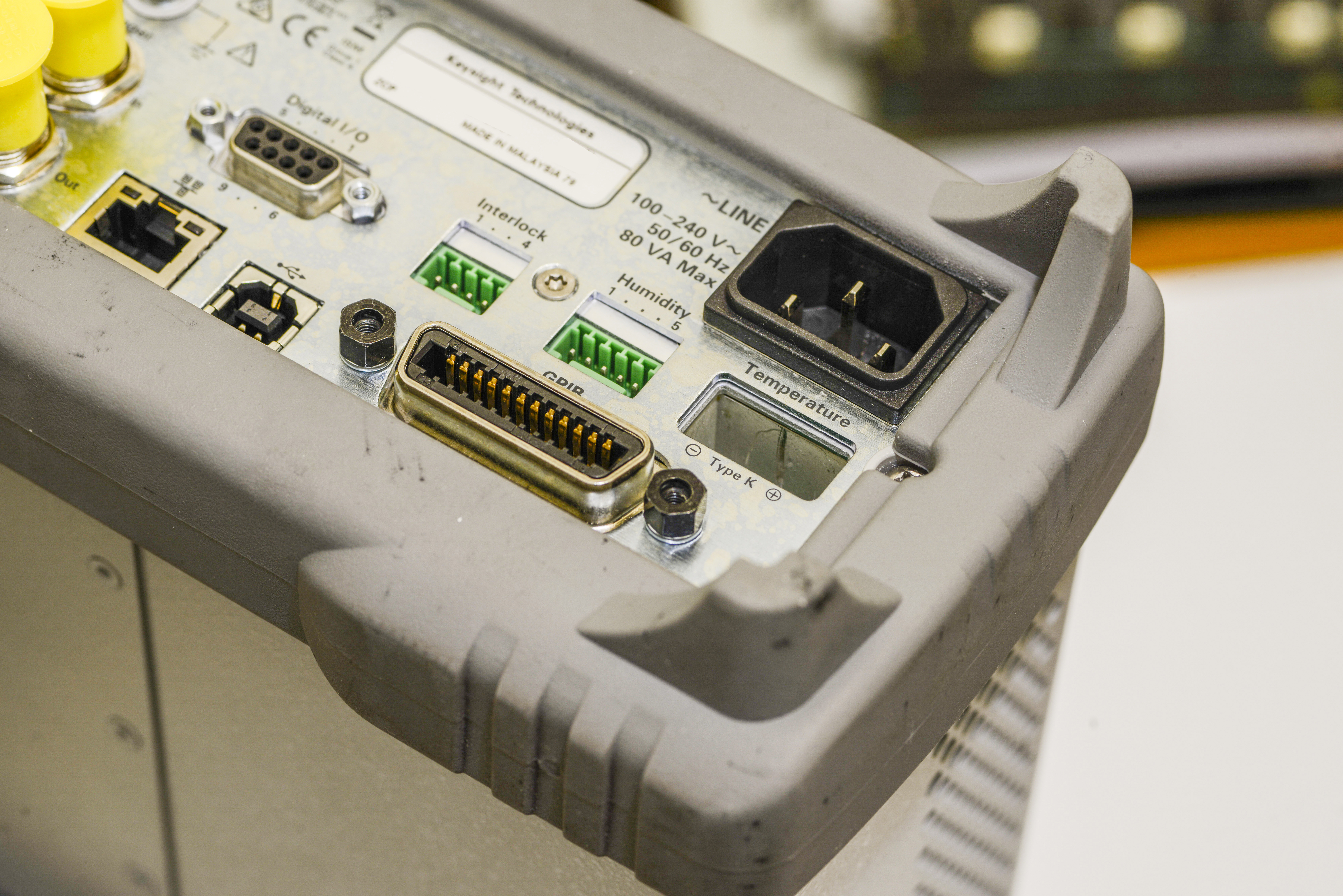
Image 8: IEC mains power input and thermocouple miniature jack for Type-K probe
Use for triaxial inputs is essential for sensitive instrument like this to prevent leakages of the current between input signal terminal and outer shield/common return. We will cover more on this topic further in the article during the circuit design review.
Operation of both current meter and voltage source is decoupled by own ON/OFF buttons to allow flexible operation and easy zero offset corrections.
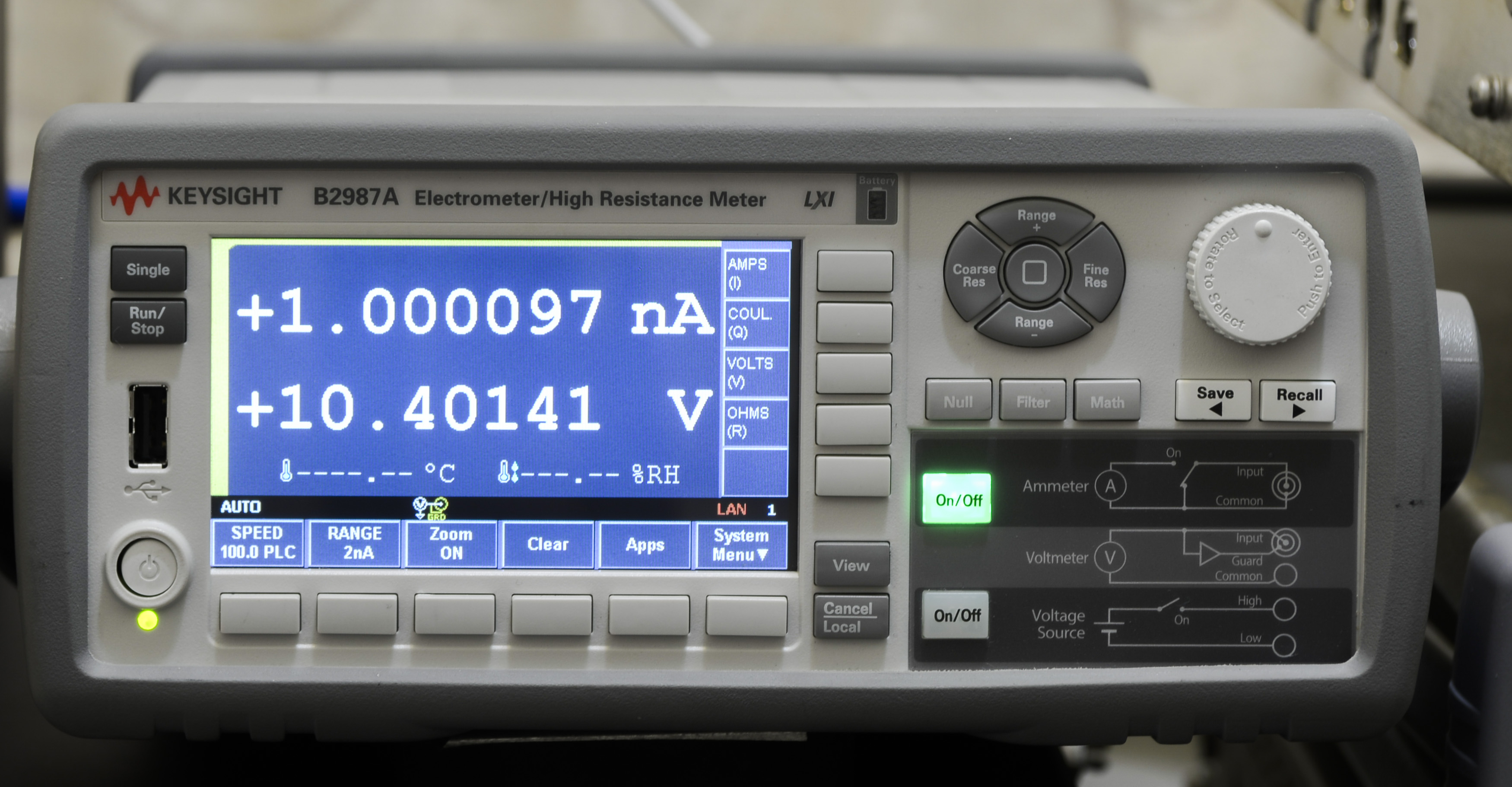
Image 9: Front panel with current meter turned on, measuring 1 nA
Design and internal design review
-1200 and +1200VDC voltages present inside of this electrometer when operation are dangerous and even lethal. Pay attention of what you are doing, and keep all connections nice and tidy. Use hands-free probing technique to ensure safety. Use tools rated for CAT III operation while servicing high-voltage live circuits in this instrument.
After removing rear bezel and metal cover with help of typical HP size Torx screwdriver internal boards are available for access. Top side reveals high-voltage output assembly, mains AC-DC switching power supply brick, battery charger PCBA and various interconnects. This is modern instrument, so majority of the components are mounted by SMT, as expected. Everything inside is organized and tidy, as you would expect from $11K professional instrument.
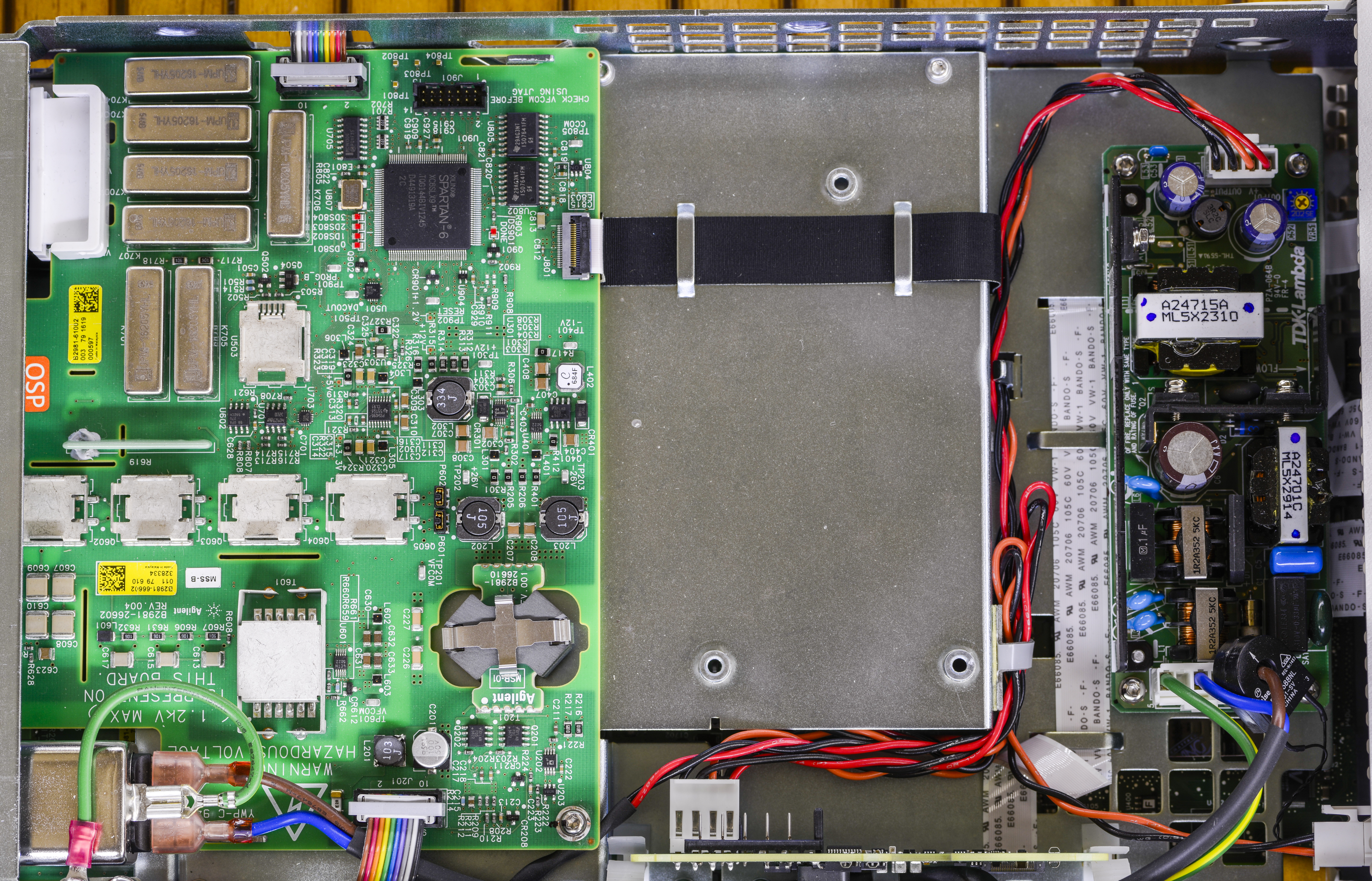
Image 10: Top side with cover removed reveals HV source, charger and main power supply
Cable harness carefully fixed to the chassis parts, so no loose wires running around. Top board in the back of the unit is high-voltage output source. B2981A and B2983A units will not have this board present.
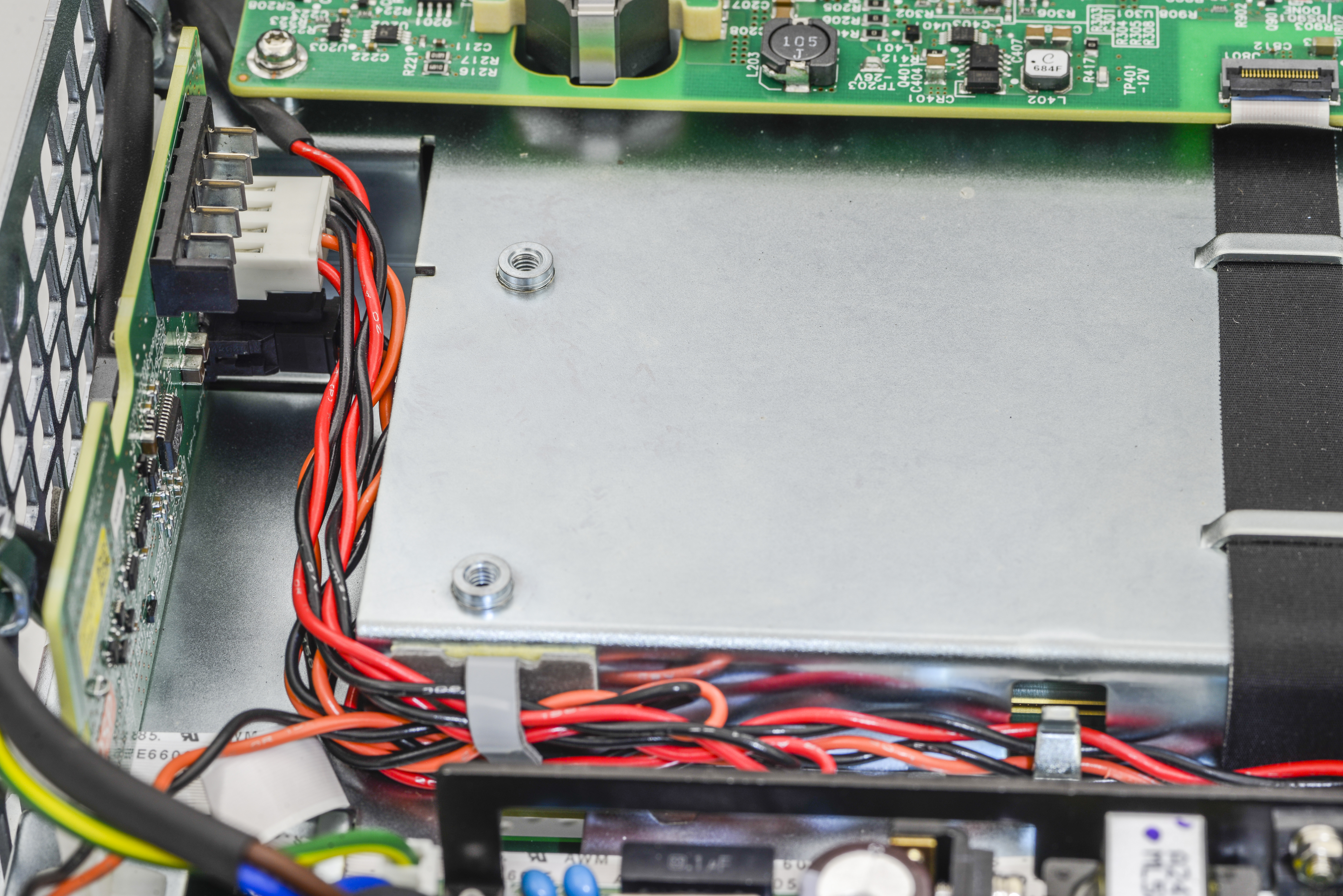
Image 11: Cable harness to charger board
Bottom side reveals back side of main acquisition board, small digital brain SOC module and multiple interconnect flat ribbon cables.
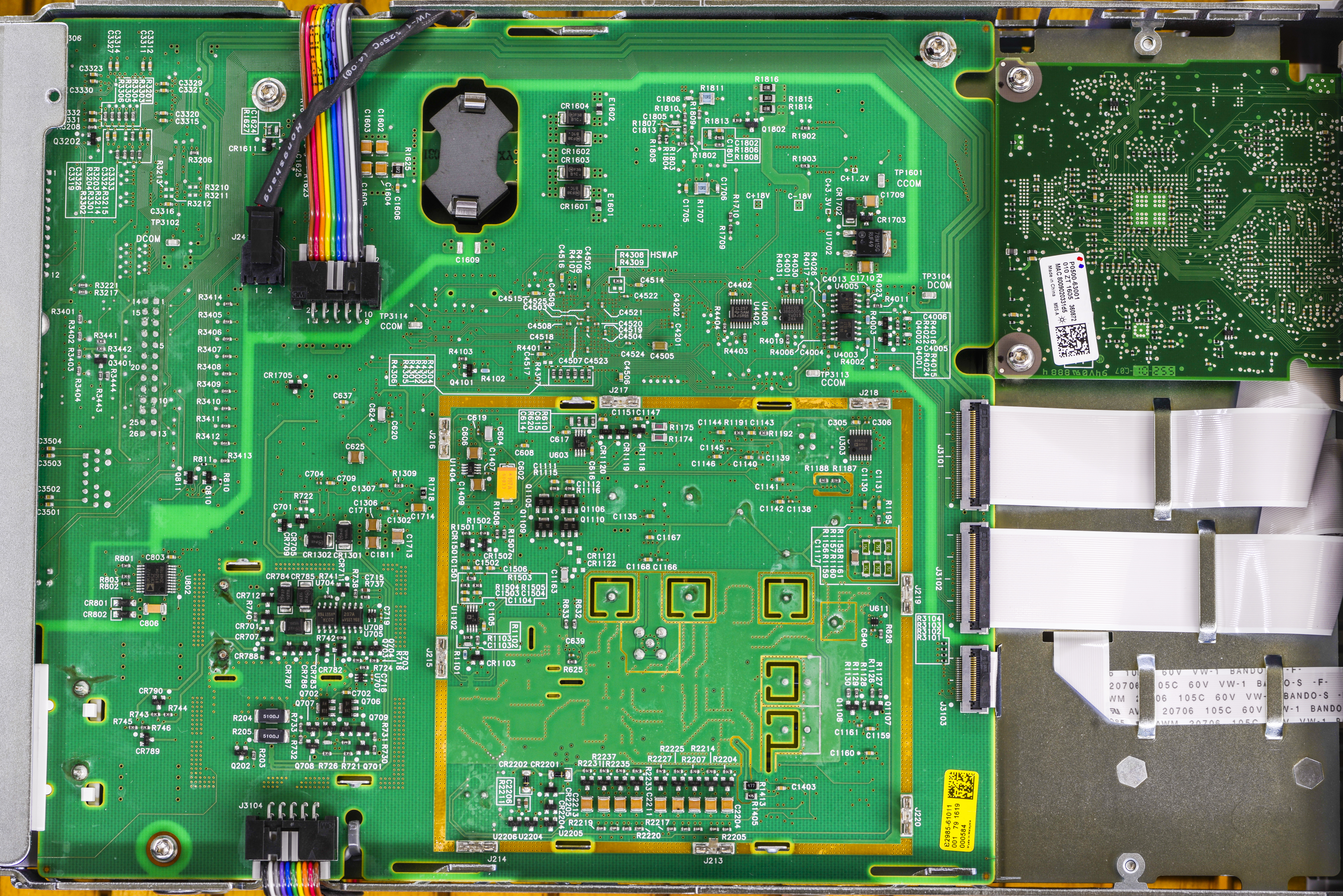
Image 12: Bottom side with cover removed. Shield on bottom board is removed for clarity
Analog board have fully shielded areas, enclused from both sides, but Image above have shield removed for clarity. Electrometer input circuitry is extremely sensitive and must be kept clean to maintain instrument’s performance, so use of proper gloves to prevent board contamination is mandatory here.
Mains AC-DC power supply
Input power supply is high-quality switching module is 50W 24VDC output, made by TDK-Lambda, model ZWS50BAF-24. It retails for $80 USD, and provides output current up to 2.1A from the universal input 85-264 VAC mains. Output noise and ripple maximum specification is 150 mV pk-pk so it is not low noise supply. It’s not a problem as this PSU output will be regulated and isolated from any sensitive circuitry by onboard POL regulators on main boards.

Image 13: AC-DC supply and front panel area
Also front panel board is visible behind the power supply. We will not be taking that part off, as there is nothing interesting on the front panel. Just Xilinx Spartan 6 FPGA with DRAM chip to handle color TFT interfacing and GUI refresh, keyboard readout and related DC-DC power for digital domain of the instrument. Most likely this front panel board reuse design from other instruments in series as well.
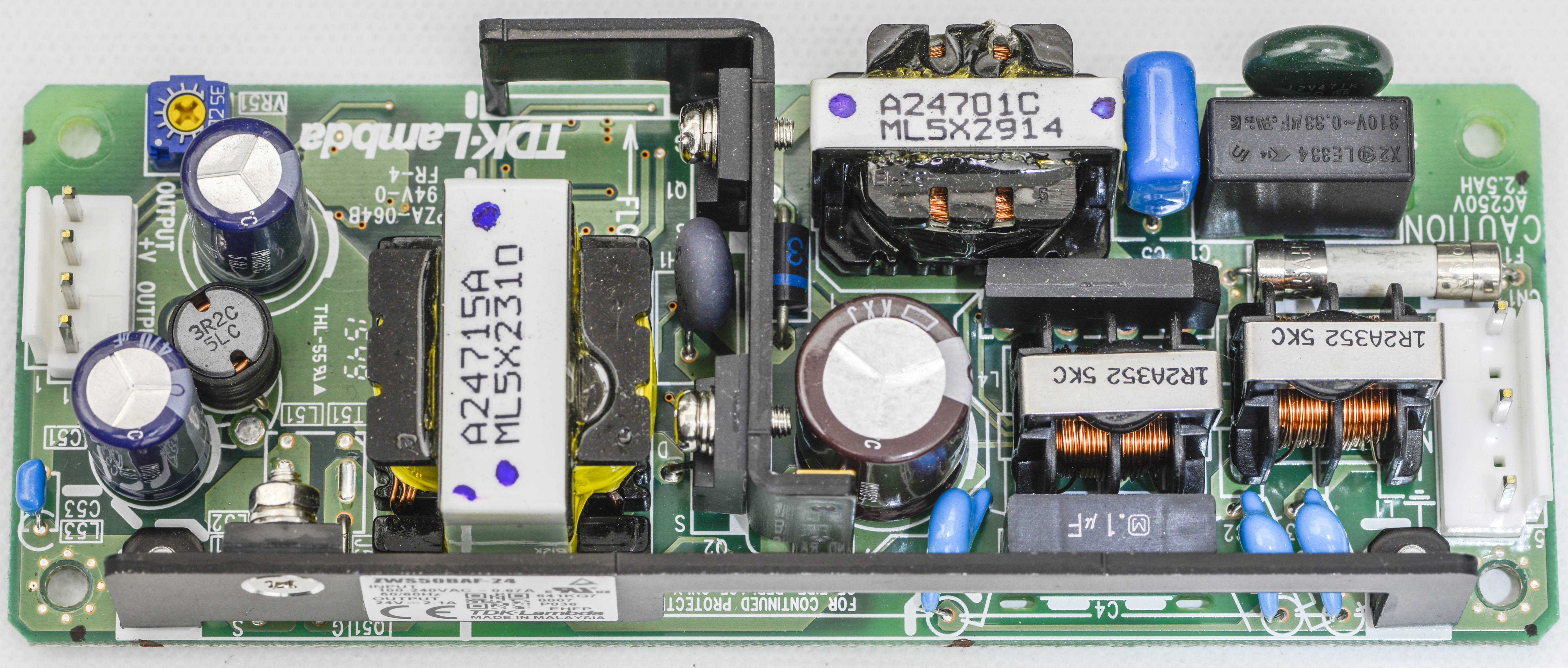
Image 14: AC-DC supply, top view
Back to power supply module, mains input arrive to the instrument from the right side connector, pass onboard line fuse, go thru passive CMC and protection components, rectified to high voltage DC by a bridge and storage capacitors and then AC/AC controller and power FET provide drive to a switching pulse transformer. AC/DC module have top tier Chemicon KXJ +105 °C rated capacitor on primary side and pair of Chemicon LXZ low-ESR +105 °C capacitors on the output side. No cheap capacitors of unknown origin, so we have nothing to complain here.
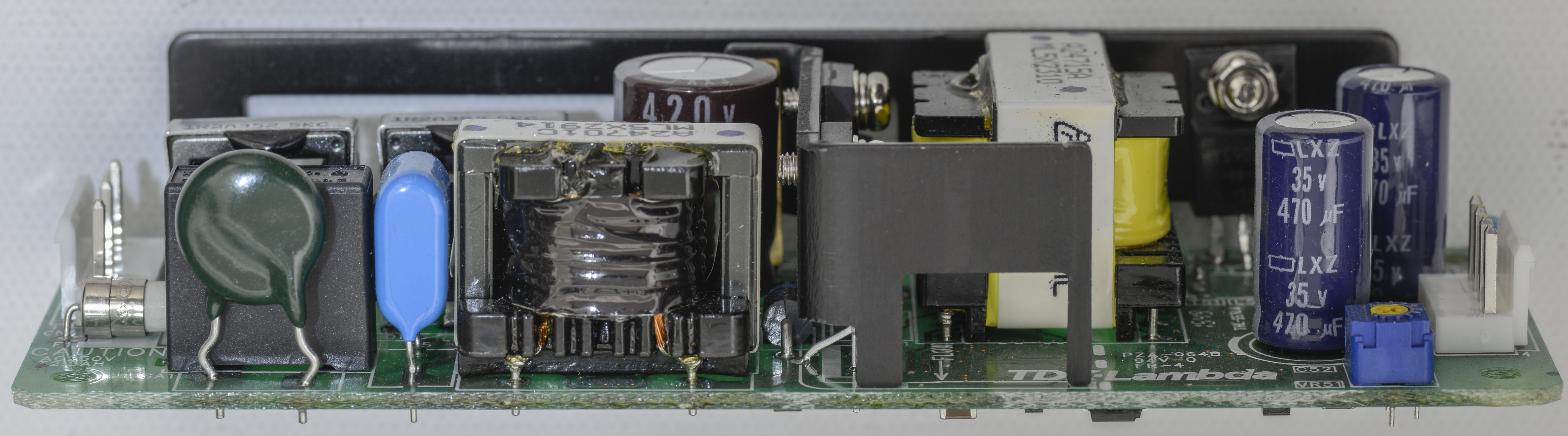
Image 15: AC-DC supply, side view
There is little adjustable trim-pot resistor near the output connector. Perhaps it’s available to adjust output voltage, if needed.
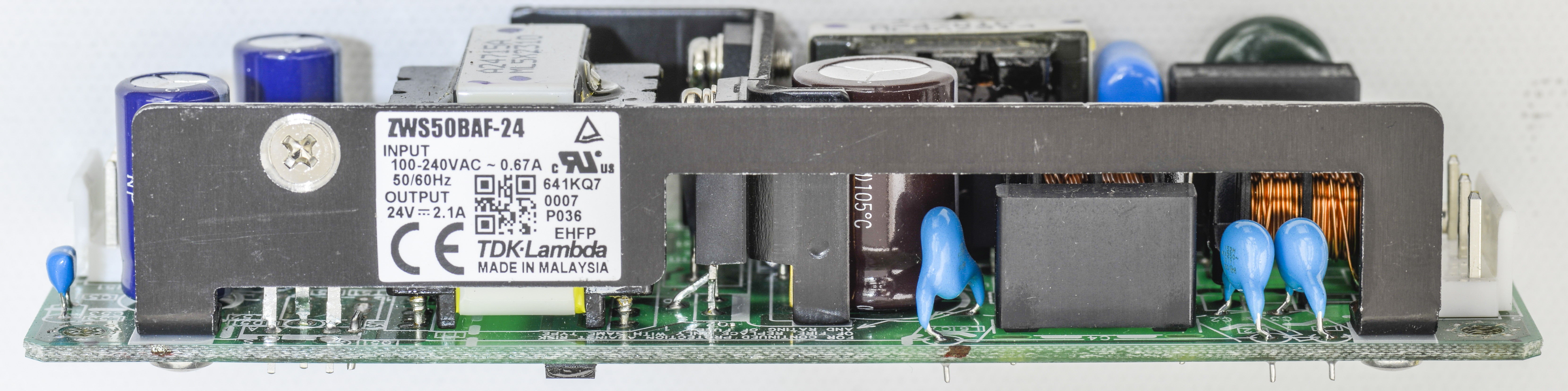
Image 16: AC-DC supply manufacturer label and power ratings
Power supply module was manufactured in Malaysia around week 49, year 2015.
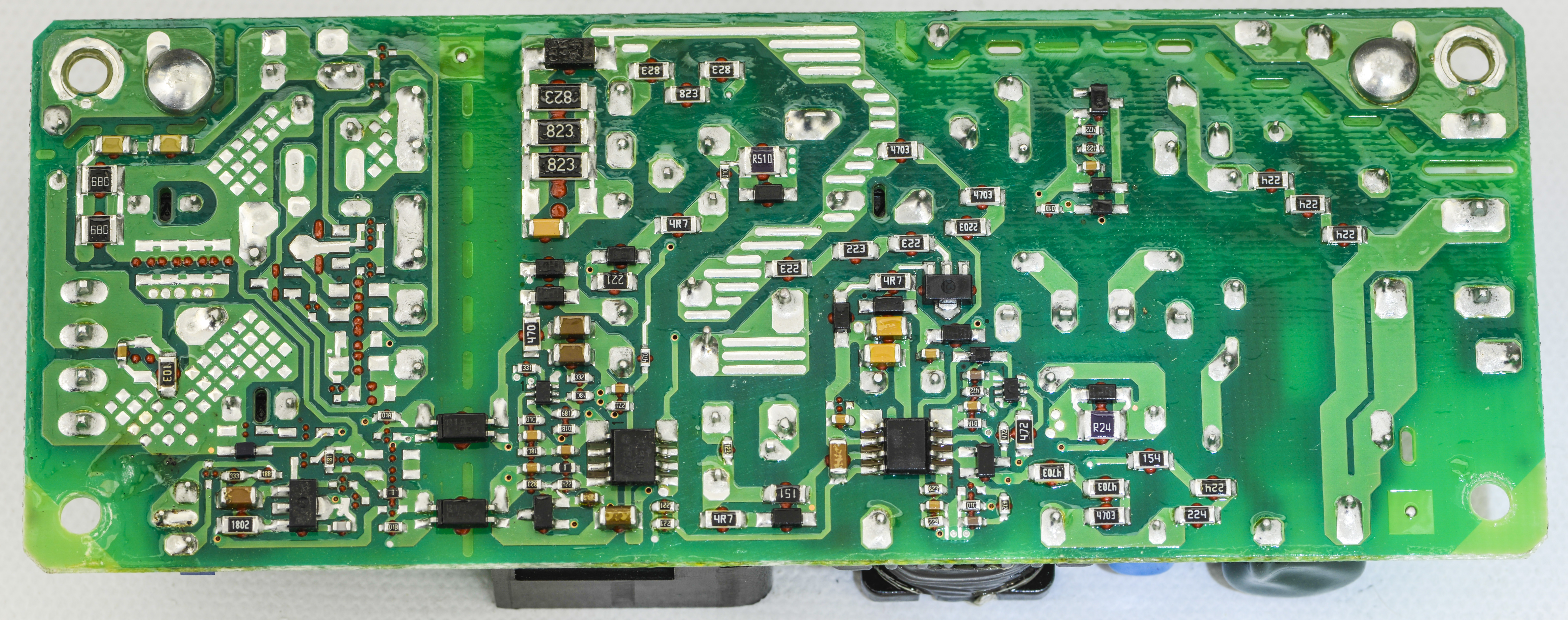
Image 17: AC-DC supply, bottom side with SMT components
Bottom side is packed with SMT components, there is room even for one tiny SOT-363 device. Most of surface mount passives are 1206 and 0603 size. Two optocouplers provide feedback signal to the high side for output regulation and protection.
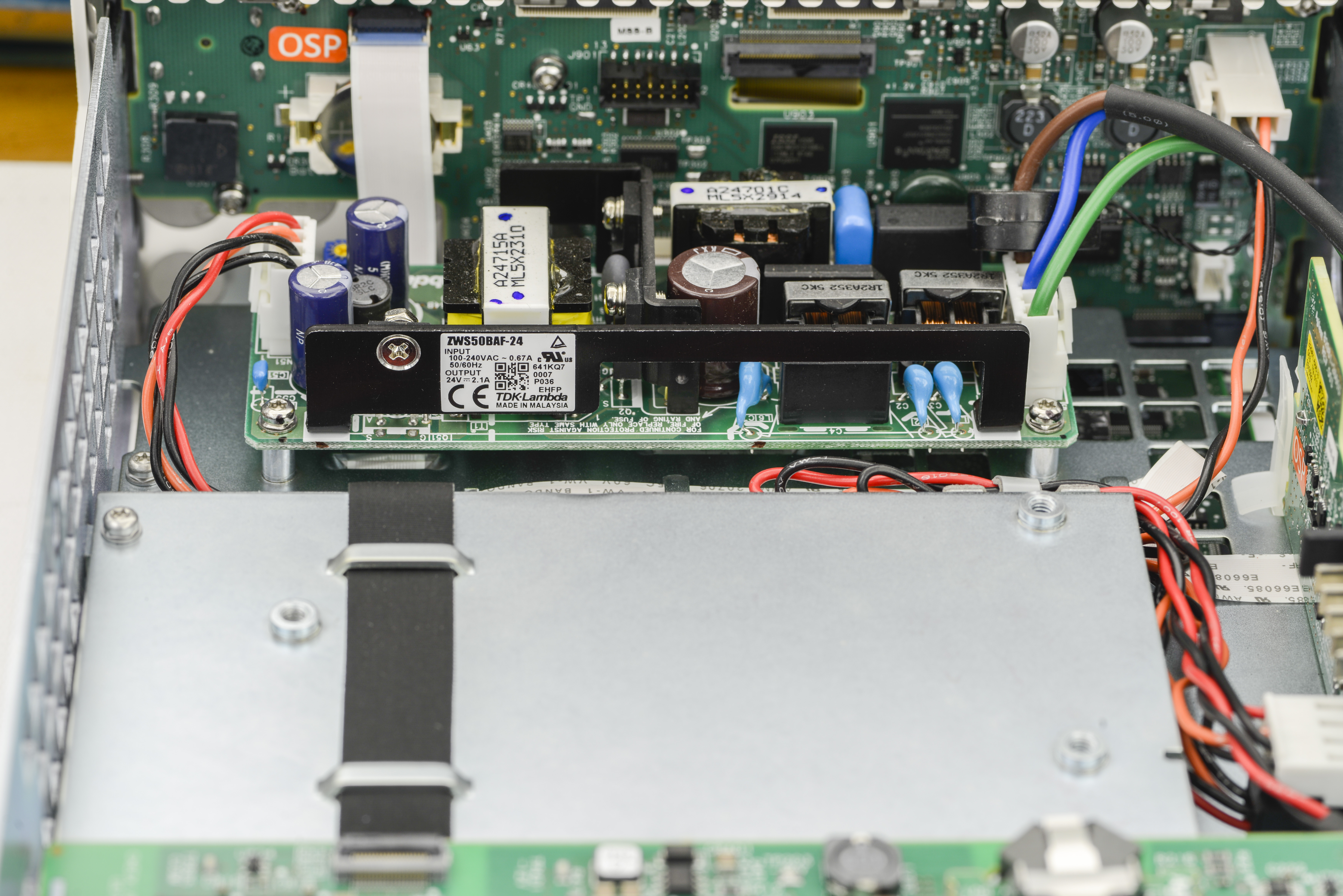
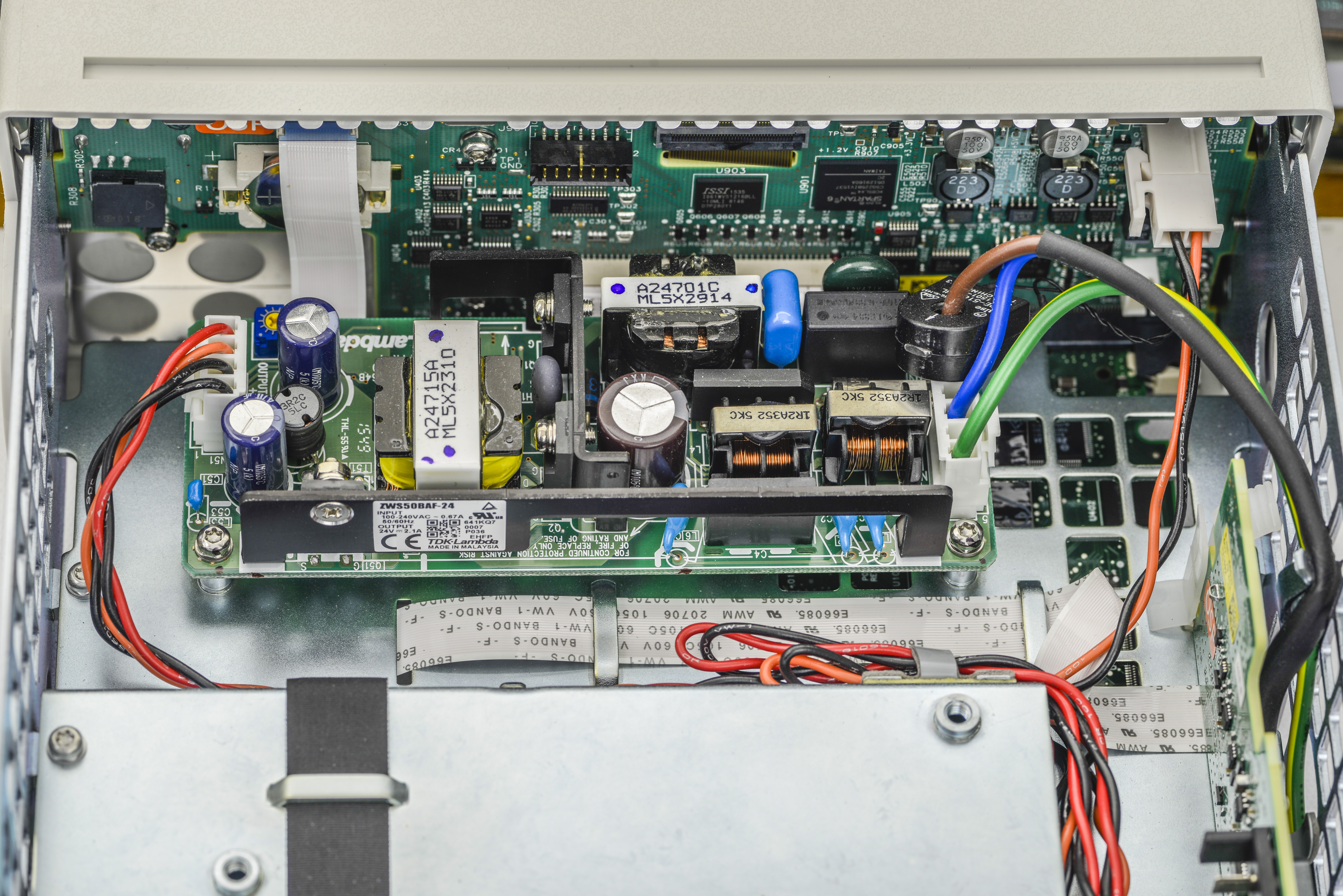
Image 18-19: Overview with PSU installed in system
Interesting detail visible on the mains cable to the power supply. Line wire before entering PSU have small current transformer, with secondary connected to front panel PCBA. Perhaps this is used to detect the mains grid frequency for automatic PLC timing setting? I see no obvious reason why meter would possible need measurement of it’s own input power otherwise.
Charger board B2981-26603 for optional battery pack (only for B2983A and B2987A)
Looking at the charger PCB it become also obvious why main AC/DC supply is selected to provide +24VDC output. As we know, battery nominal voltage is 14.4V, so charger circuit should receive higher voltage for good regulation margin. Based on Rev.003 label Keysight engineers had few revisions to get this little charger module working properly before entering production in this unit.
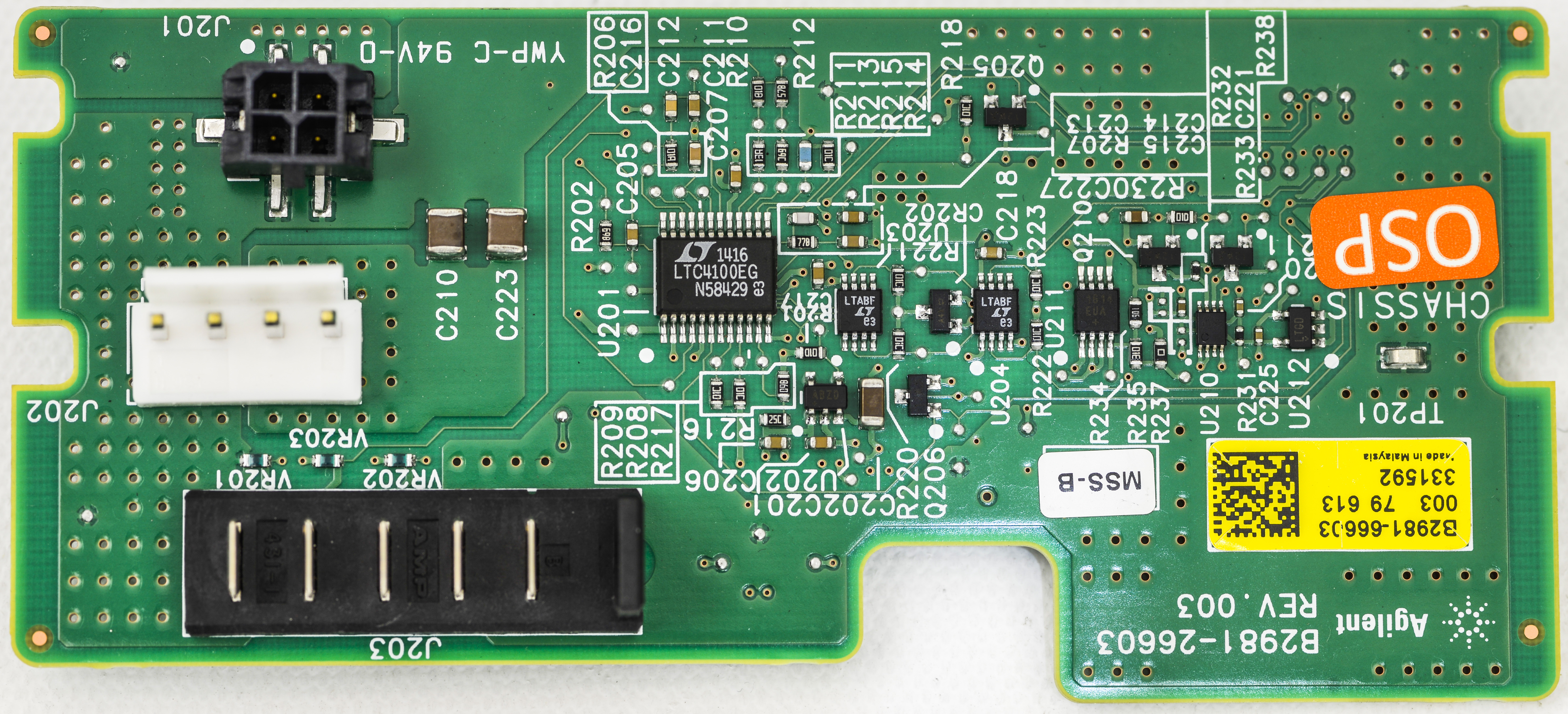
Image 20: Battery charger module, top side
Board still have Agilent logo, and date code on Linear (today part of Analog Devices, sadly) LTC4100EG charger controller reveals manufacturing period around week 16, year 2014. LTC4100EG is Smart Battery Charger Controller with digital SMBus telemetry support, wide 3.5 to 26V output voltage range and up to 4A of charging current capability. It is rather complex all in one chip with lot of functionality and protection available for safe charging and battery management.
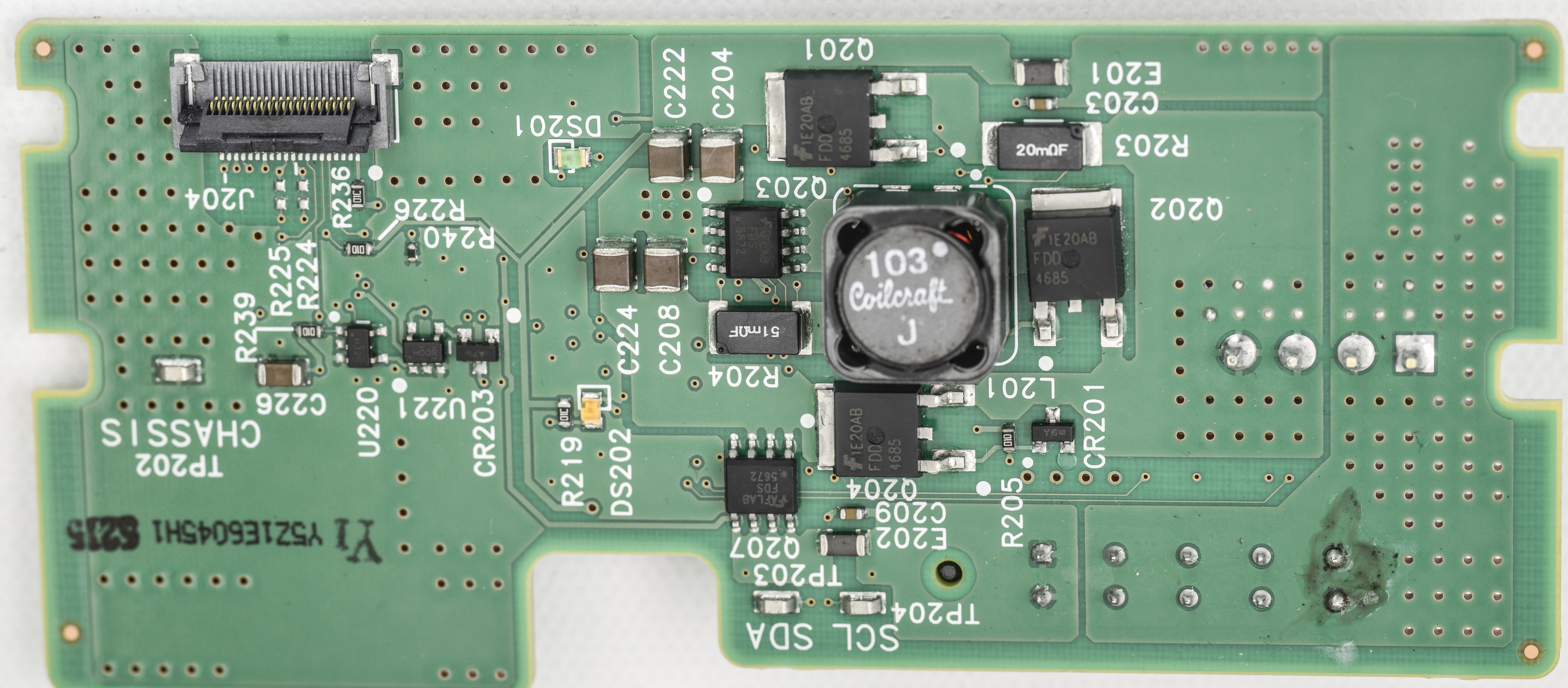
Image 21: Battery charger module, bottom side with power components
Rear side of the board also have components populated. These include pair of ON Semi FDS5672 60V N-channel MOSFETs, three ON Semi FDD4685 -40V P-channel MOSFETs, Coilcraft inductor, some 1210-sized MLCCs and two shunts for current monitoring. There is tiny DS201 green LED for charge indication and couple of test points, marked SDA and SCL. These are obvious related to SMBus interface and available for easy probing.
Keysight does offer battery as an option N1418A, however priced at $871 USD for US market that is almost five times over the original RRC2024 pack. Benchtop charger available from Keysight, option N1419A goes at $1081 USD, clearly targeted for enterprise/business market customers.
Original battery from OEM manufacturer that Keysight use for B2987A is Lithium-ion pack RRC2024. This battery have 6600 mAh capacity, rated for 14.4V and supports up to 4.6A charging current. It have internal cell 4-series 3-parallel (4s3p) topology. We have already ordered 3rd party battery to try in unit in standalone operation.

Image 22: Battery blade connector
Battery and charger interface using blade-type connector, typical for power packs. There are five contacts to provide power and telemetry connection between the unit and the battery pack. According to the user’s manual operation time on battery power for fully featured B2987A listed as mere 5 hours. Picoammeter B2983A without high-voltage source specified for 7 hours of battery life. This gives us some interesting math to guess.
Meters power consumption = 95.0 WAh / 5 hours = 19 W. Two extra hours between the units means that high-voltage output option board takes about 5.4W of power alone. Would be interesting to know power savings possible if one would ditch power-hungry TFT front panel interface and its related FPGA logic? Hint to Keysight for NFP-version of the instrument for production test rigs :)
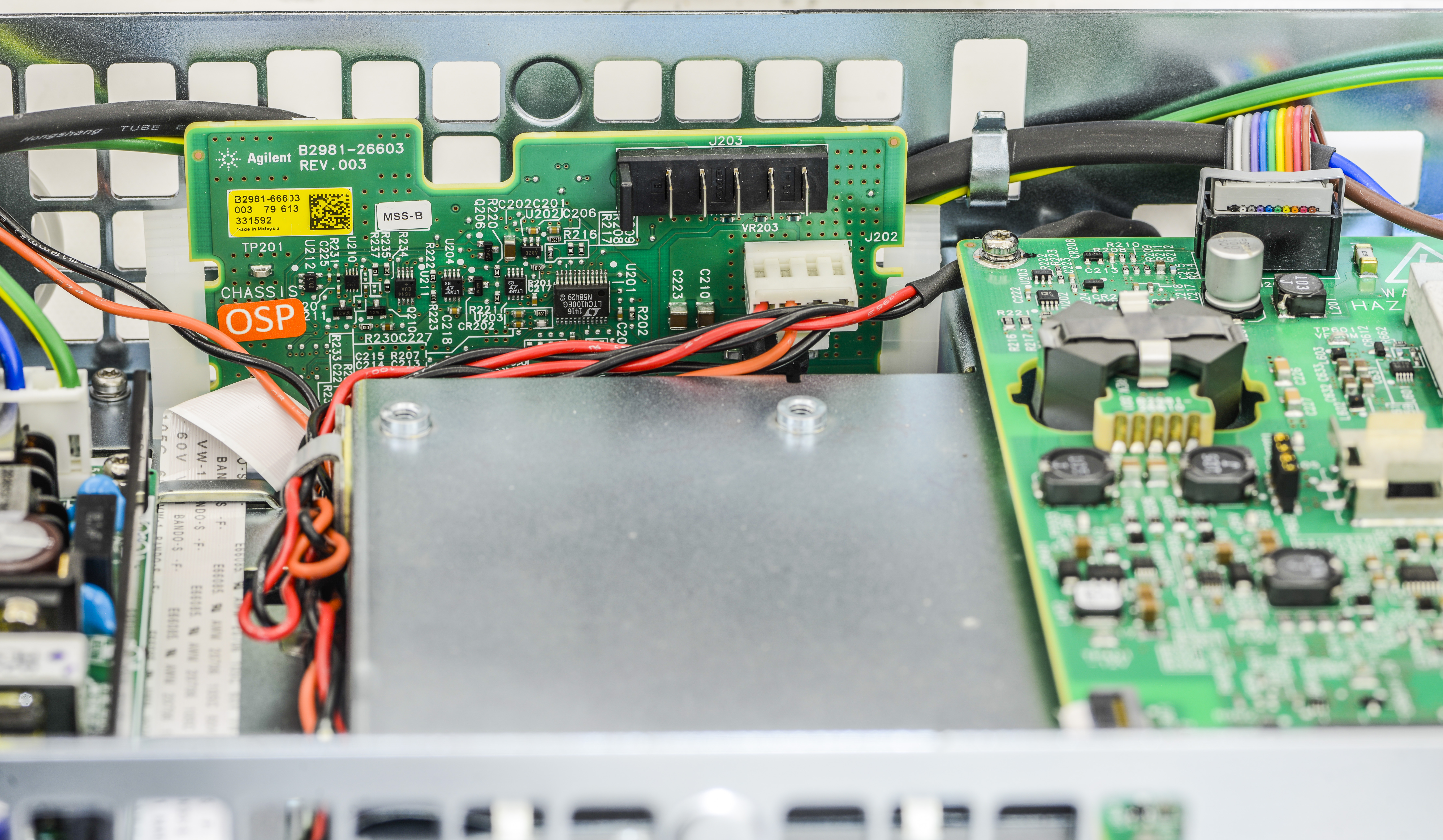
Image 23: Battery charger assembly installed in the meter
Interesting design note – charger board does not have rigid mount to the chassis and have small movement freedom. Two plastic holders keep the board in place, but allow flex to prevent contact damage and excessive stress during battery pack replacement/installation.
Main processor board / module P0500-63001
Heart of the digital sub-system is STMicro SPEAr eMPU with support of Xilinx Spartan-3E FPGA. Xilinx FPGA provides acceleration and additional I/O for the SPEAr SOC to help interfacing all those peripherals onboard of B2987A.
Processor board is not unique design only for this instrument, but shared module design. It is also used in other Keysight instruments like B2900A series SMU, Agilent/Keysight 532xx series frequency counters, arbitrary signal generators. Some Keysight 1000X/2000X/3000 X-series oscilloscopes also share similar CPU topology.
Small investigation work revealed that Keysight B2987A running Windows Embedded CE 6.0. One hardware hacker even discovered how to run legendary DOOM game on his Keysight DSOX1102G oscilloscope. Maybe next step is to try Quake on B2987A electrometer? ;)
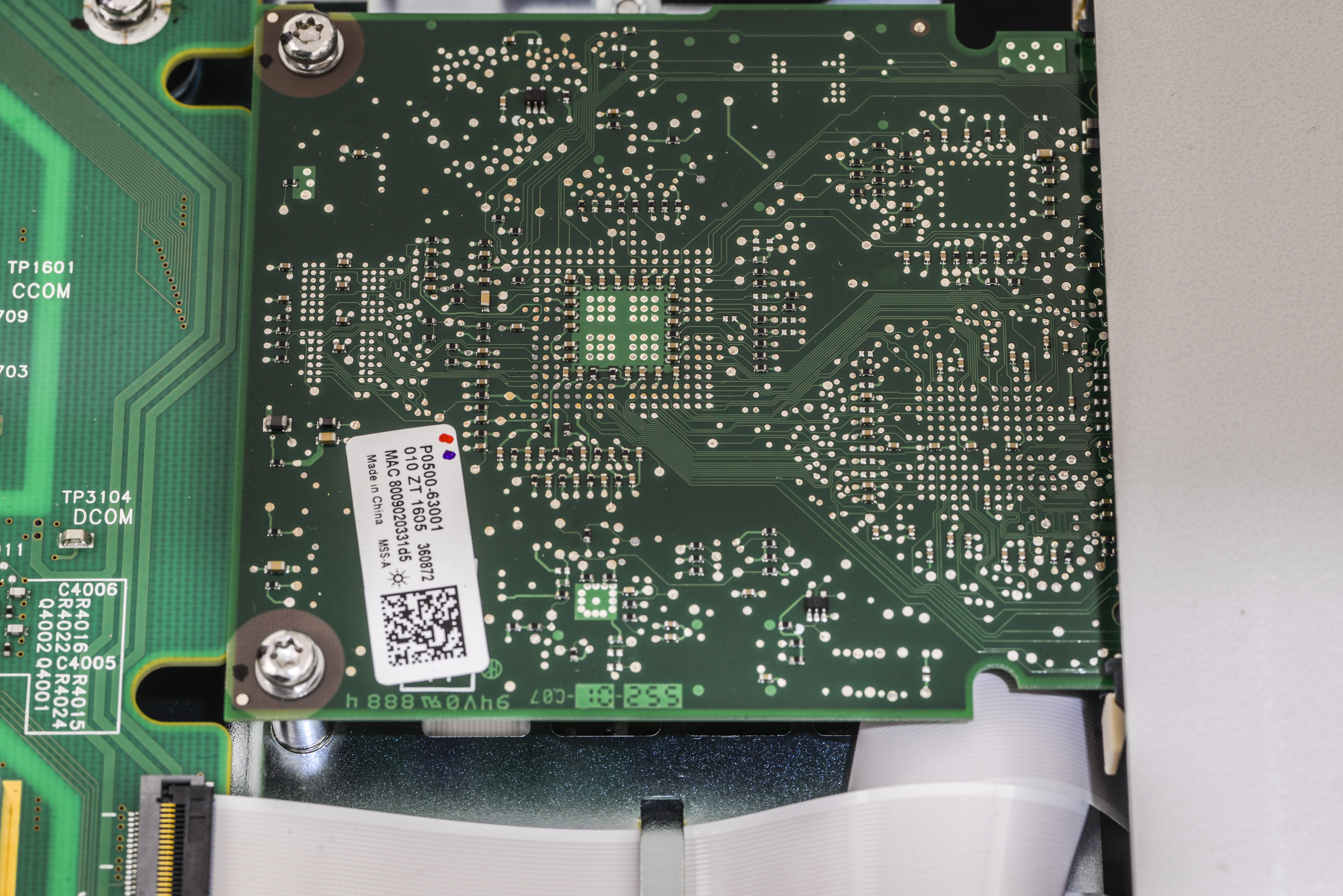
Image 24: Main processor board
This board use mechanical SO-DIMM type slot to interface with front panel PCBA. This allows easy development and reuse of the existing design in various instruments and not uncommon concept in world of mixed-signal instrumentation. Board have metal U-shape plate glued to the processor (main BGA chip in center) to provide additional surface area for better thermal performance.

Image 25: Edge card connector for CPU module
We can also find 63-VFBGA (9 × 11 mm) package with marking NQ432 is Micron MT29F1G08ABADAH4-ITX:D NAND Memory with 1Gb (128M x 8) capacity and parallel interface. It stores OS and firmware code of the instrument. This NAND Flash is already EOL’d in February 2018 by the manufacturer, but reference price for it was about $3.5 USD a piece.
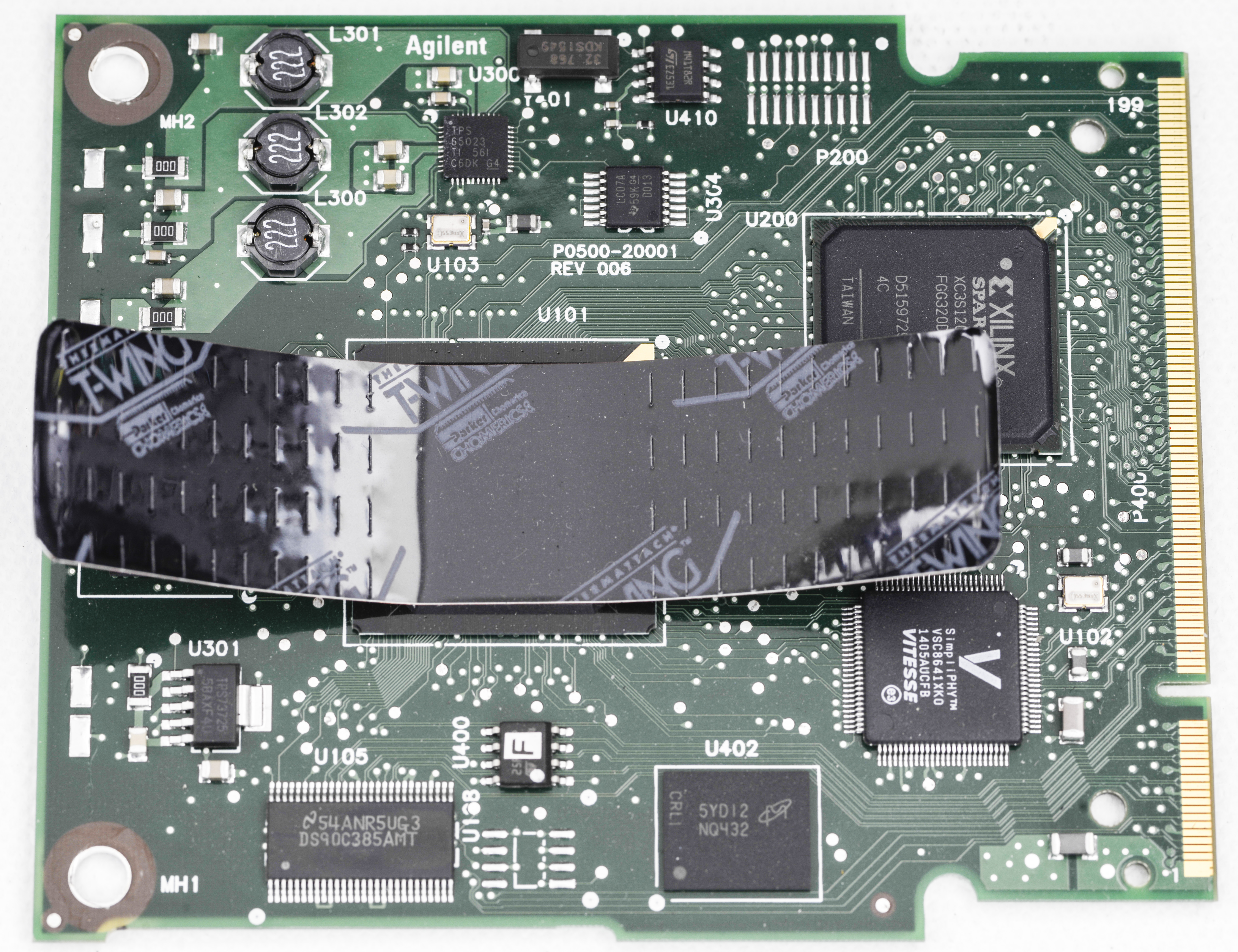
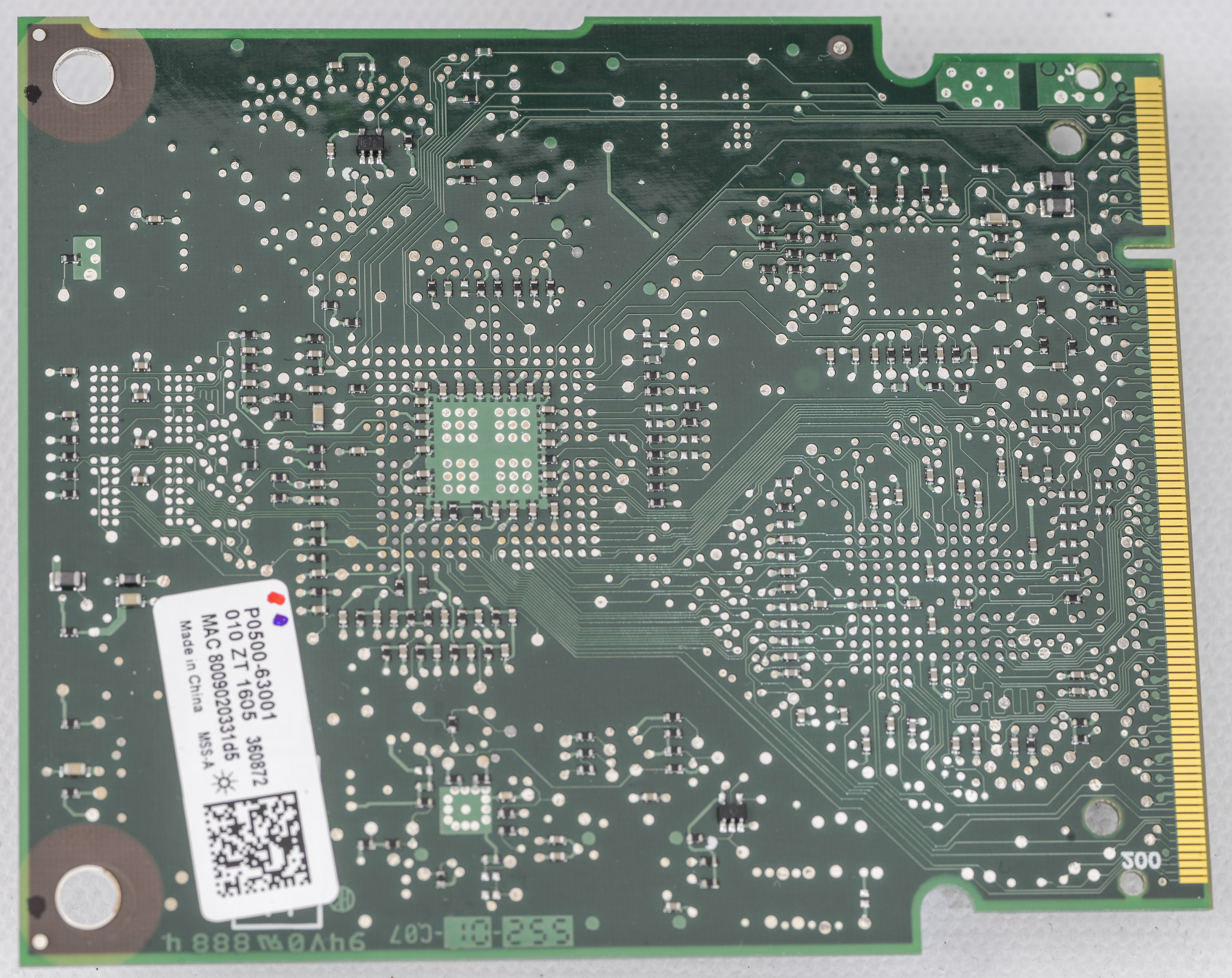
Image 26-27: CPU module top and bottom sides
TI DS90C385AMT in TSSOP package is programmable LVDS Transmitter, designed to convert parallel 24-bit RGB bus from SPEAr processor into serial Flat Panel Display Link. This interface is quite similar to other modern display interfaces, but adapted for flat-panel interconnect.
Another Texas Instruments part – TPS73725 1 Amp LDO take care of memory bus termination voltage and related power delivery. Vitesse VSC8641XKO is low-power 1GbE MAC+PHY interface chip that handle LAN/LXI connectivity of the instrument.

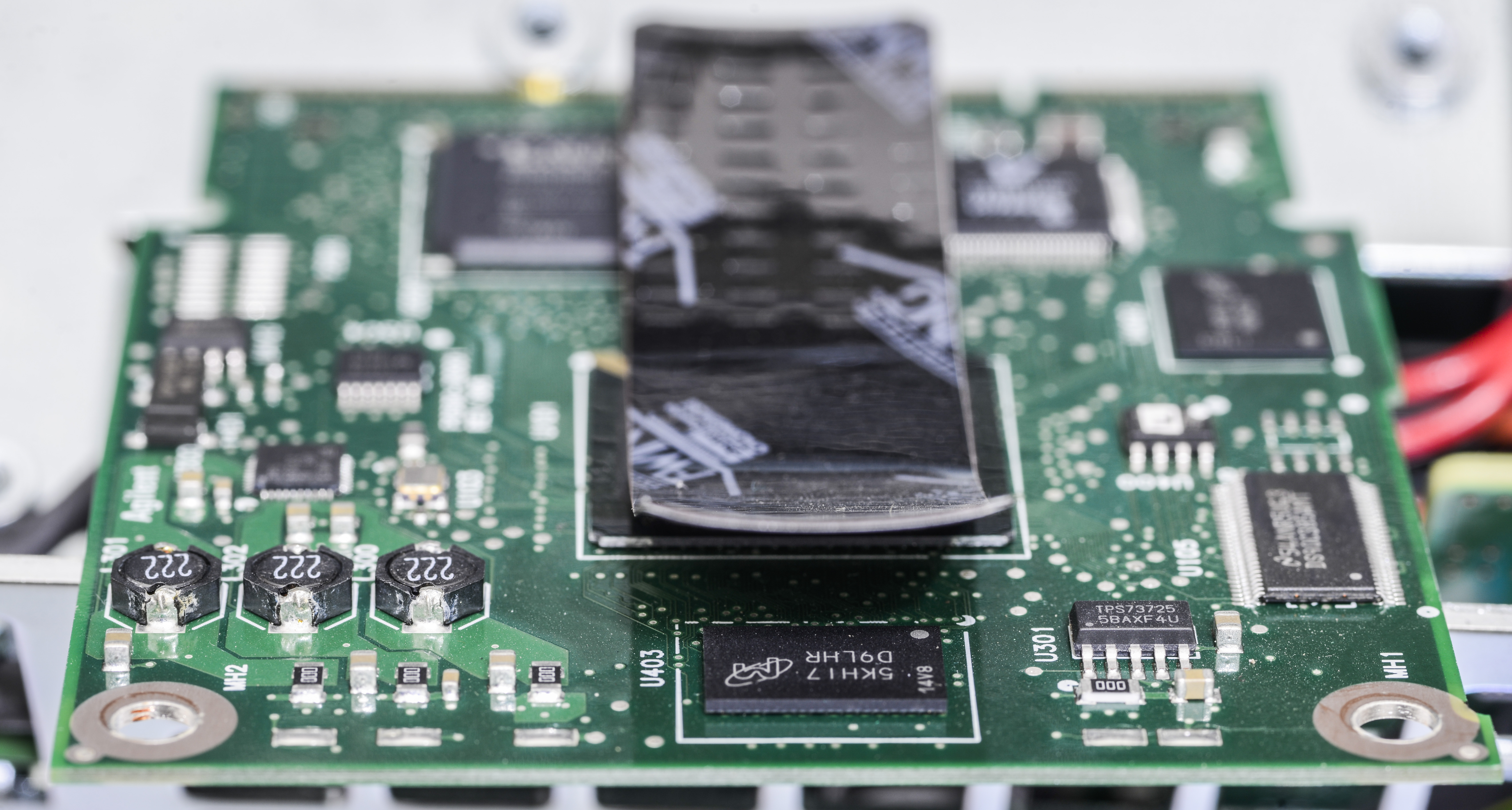
Image 28-29: Side view, unveiling FPGA and DDR2 SDRAM marking
84-FBGA (8 × 12.5 mm) D9LHR hiding under the heatsink plate is Micron MT47H64M16HR-3:H DDR2 SDRAM chip, also with 1Gbit capacity organized as 64M x 16 bit parallel bus. This lowest-grade 3ns RAM rated to run at 333 MHz (DDR-667 effective).
We can also find various support components, 32768 Hz XO for RTC timekeeping function and main power regulator, based around Texas Instruments TPS65023 PMIC. This regulator have three separate switching DC/DC regulators for SoC/FPGA power and three LDO regulators for auxilary power. There is even serial I2C interface for management and telemetry.
High-voltage output board B2981-66602 (only for B2983A and B2987A)
This assembly generate programmable voltage output in either polarity with two available ranges. With only 1 W of available power it is not high power, but suitable for many biasing applications and test conditions.
| Voltage Source | Output current | Output accuracy | Resolution | Noise, 0.1-10Hz (10Hz-20MHz) |
|---|---|---|---|---|
| ± 20 V range | ± 20 mA | 0.05 % + 2 mV | 700 µV | 55 µVpk-pk ( 1.6 mVRMS ) |
| ± 1000 V range | ± 1 mA | 0.05 % + 100 mV | 35 mV | 2.6 mVpk-pk ( 3.0 mVRMS ) |
Table 3: Voltage source ranges and specsheet
Voltage ranges and specifications are presented in detailed table. This voltage source can also provide sweep (linear or list of values) and ARB (square) mode for complex experiment requirements.

Image 30: Rear high-voltage source overview
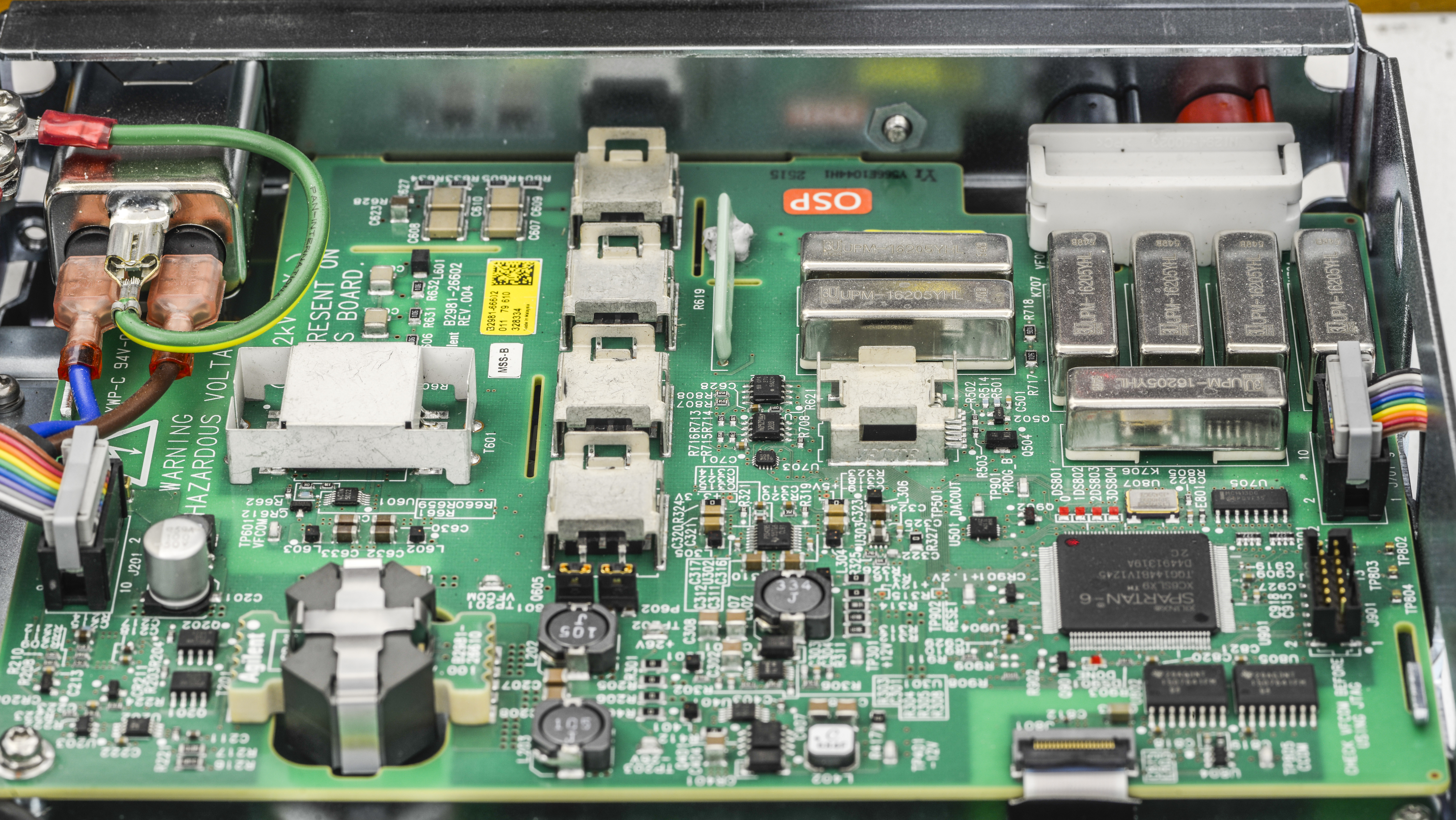
Image 31: test
Image 32: test
Interconnect for HV source is done via two 100 mil pitch 10 pin headers located on sides and going to main analog board. Digital control and programming performed thru FPC ribbon cable, close to digital isolators.
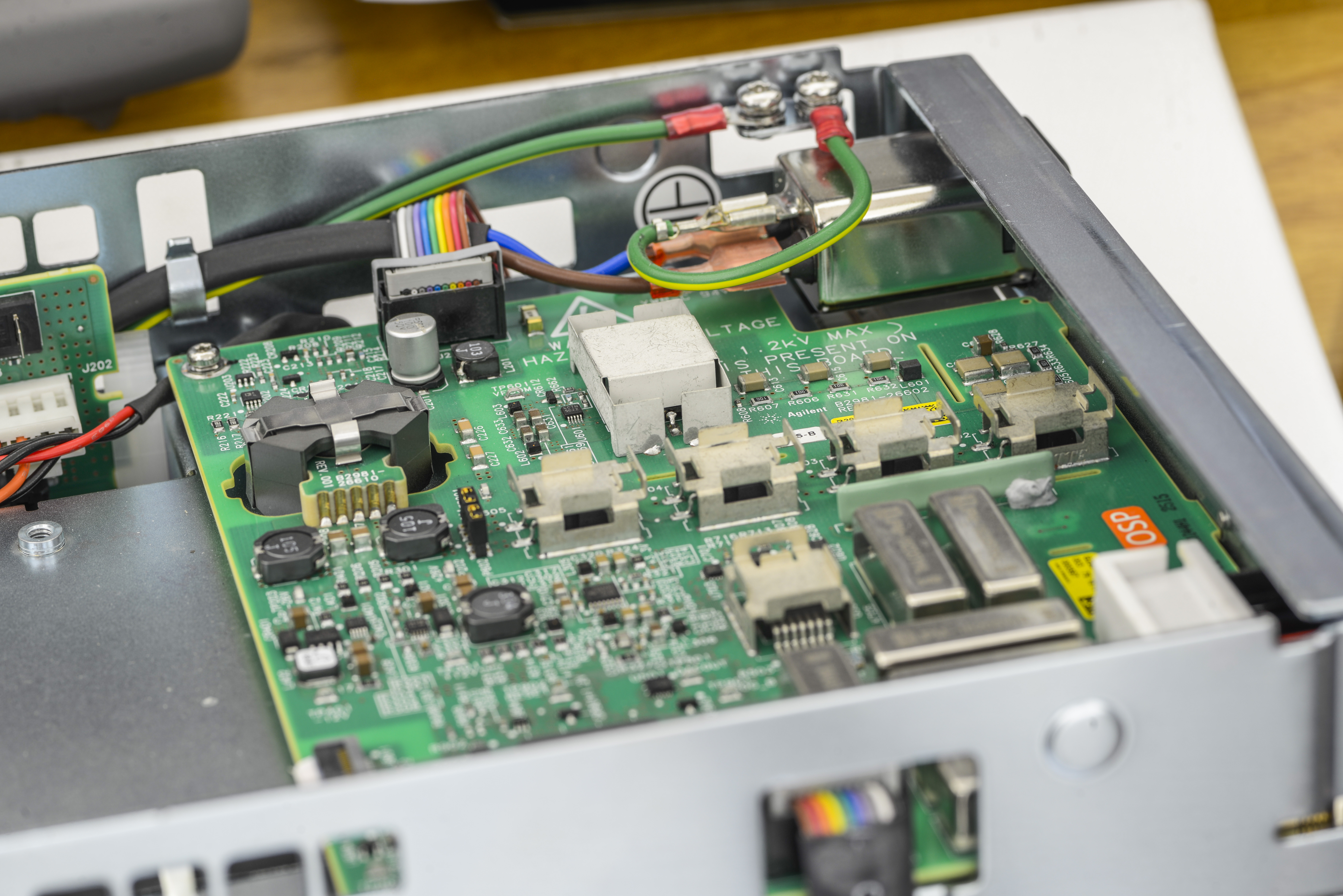
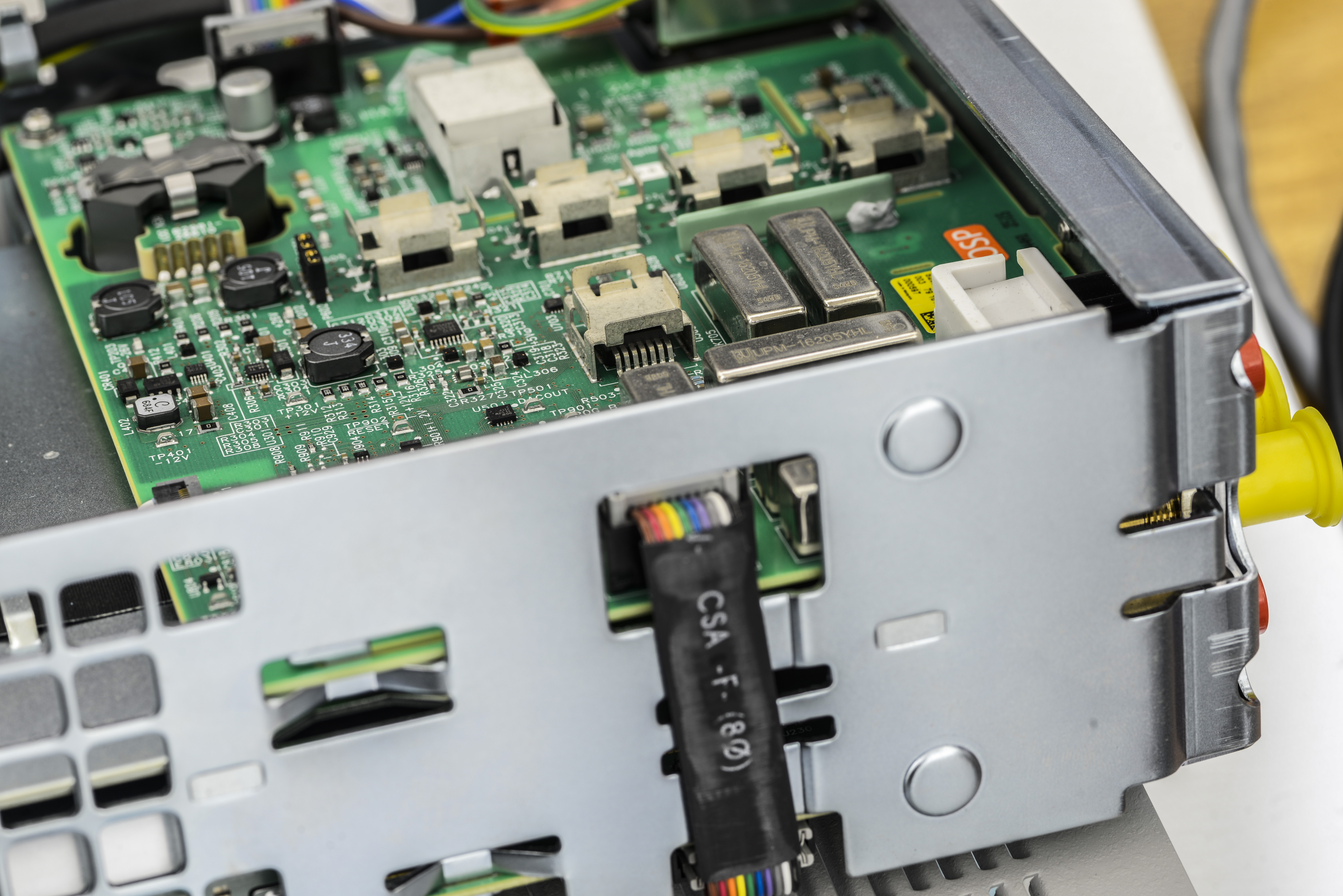
Image 34-35: test
All active power devices have heatsinks mounted on them to help with thermal management. Unit does not have fan, so board location on top, right under the chassis vents definately helping here.
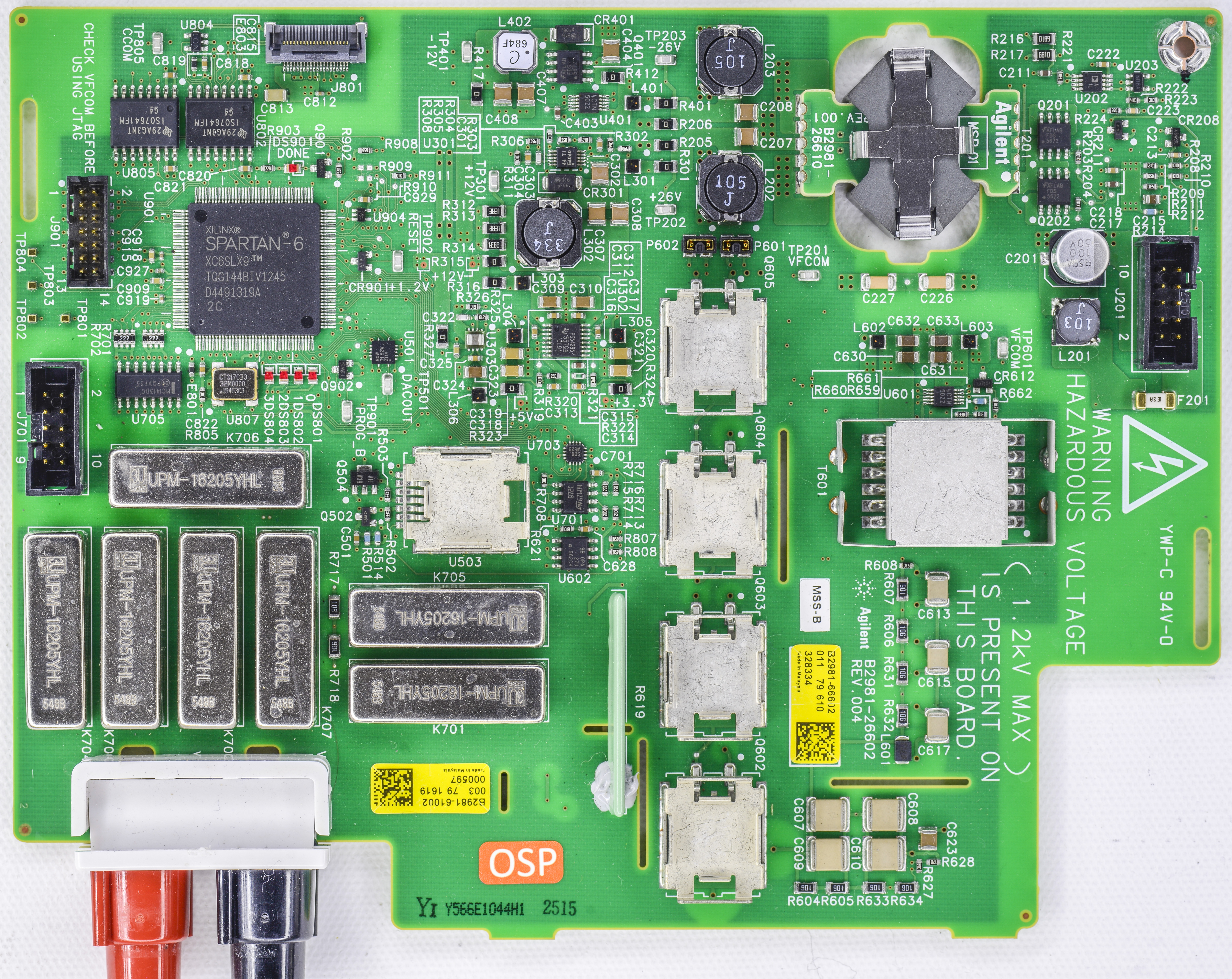
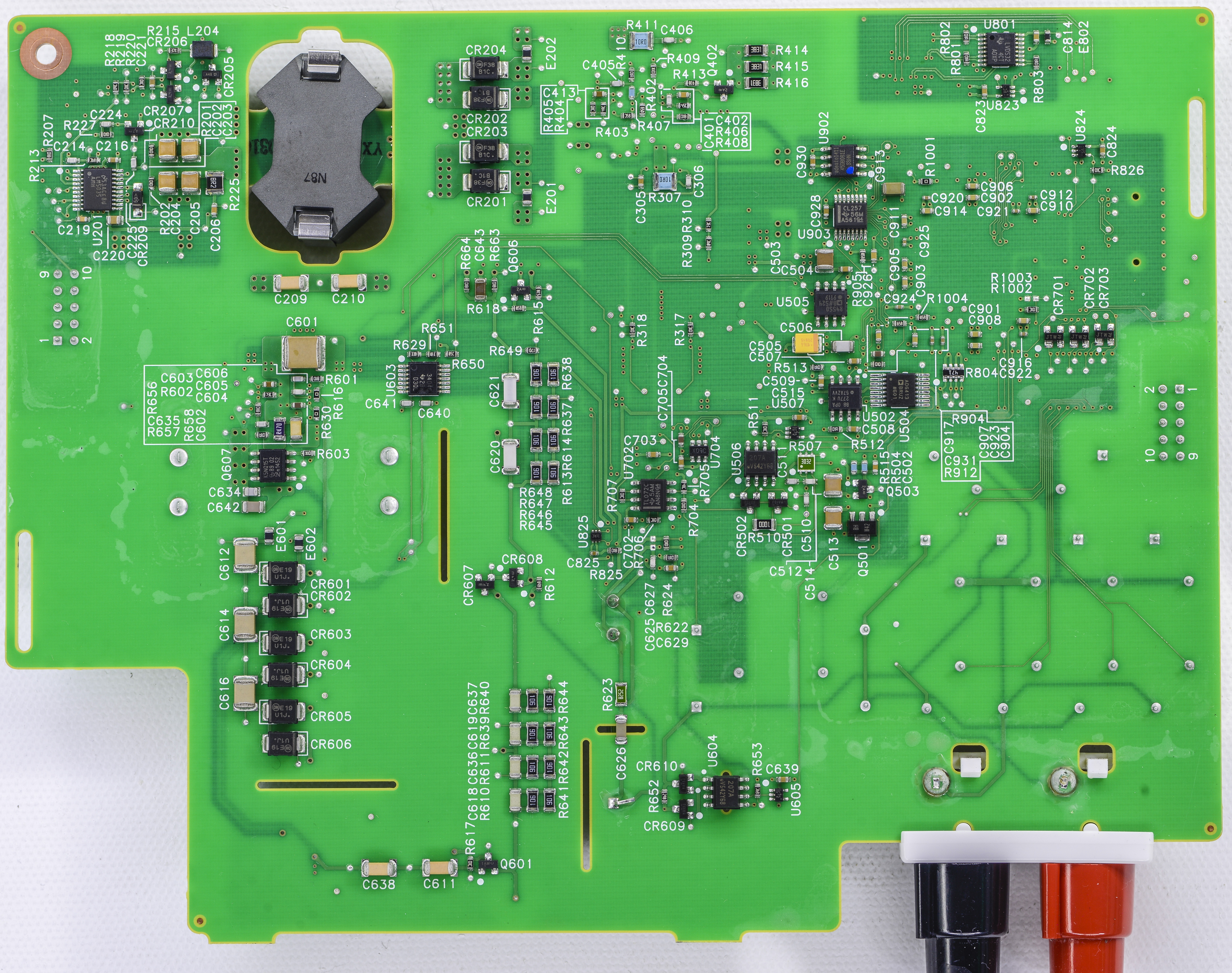
Image : HV board removed from the chassis
This PCBA is using 6 layers and have components populated on both sides. There are no special requirements for high leakage isolation so we don’t see much guarding or slots here.
High voltage reed relays are manufactured by TPM Sanyu Electric Model UPM-16205YHL designed for 1000V switching voltage and insulation resistance minimum 100 GΩ. Relay contacts rated to switch currents up to 1 A, way over the specification of the B2987A HV output. Relay activation coil voltage is 5V, and this type is non-latching.
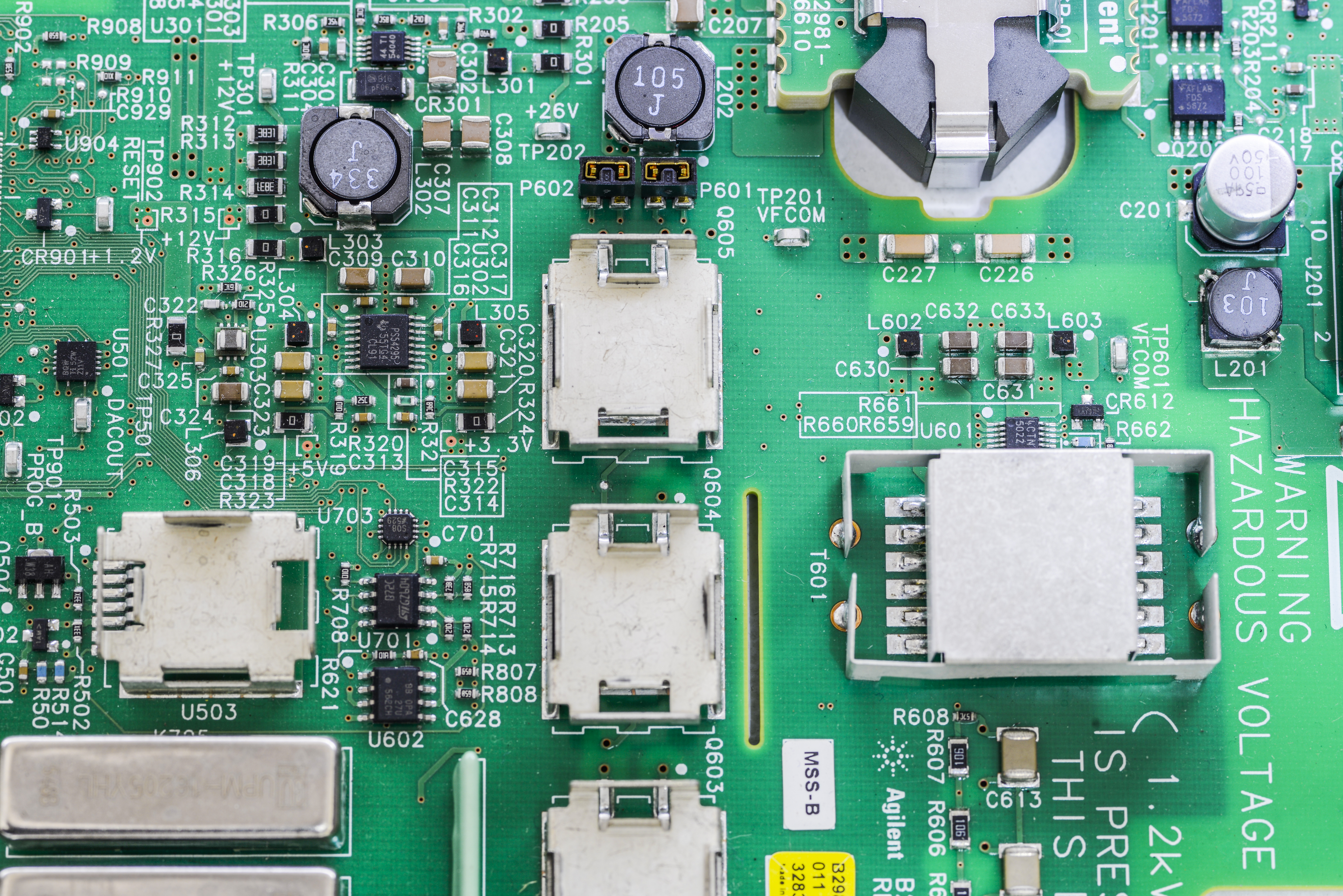
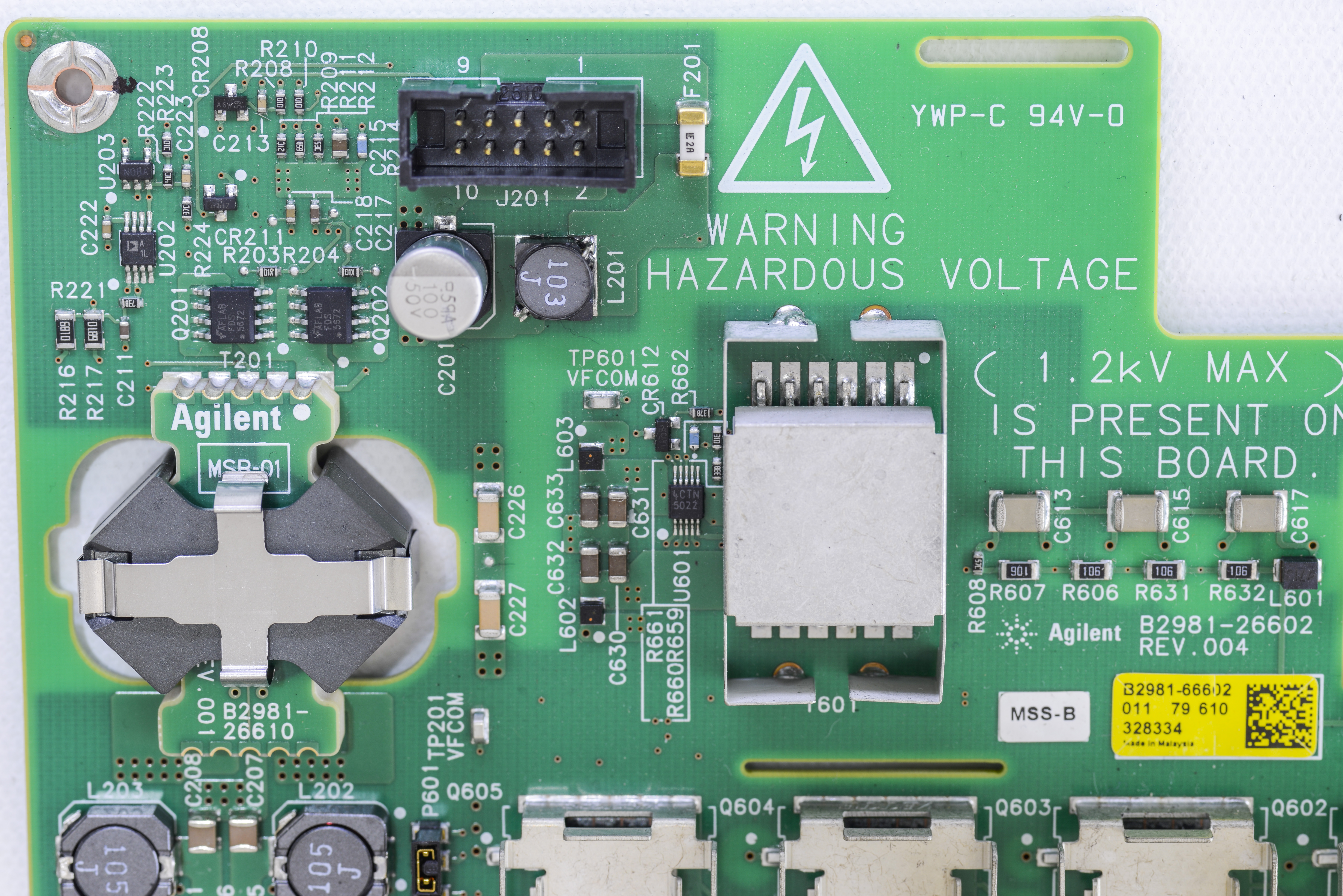
Image : test
Galvanic isolation between high-voltage assembly and rest of the instrument provided by pair of Texas Instruments ISO7641FM 6kVpk low-power digital isolators. Each of these have four independent channels and rated for isolation at least 4200 VRMS. This is quite fast isolator with 7 ns typical propagation delay.
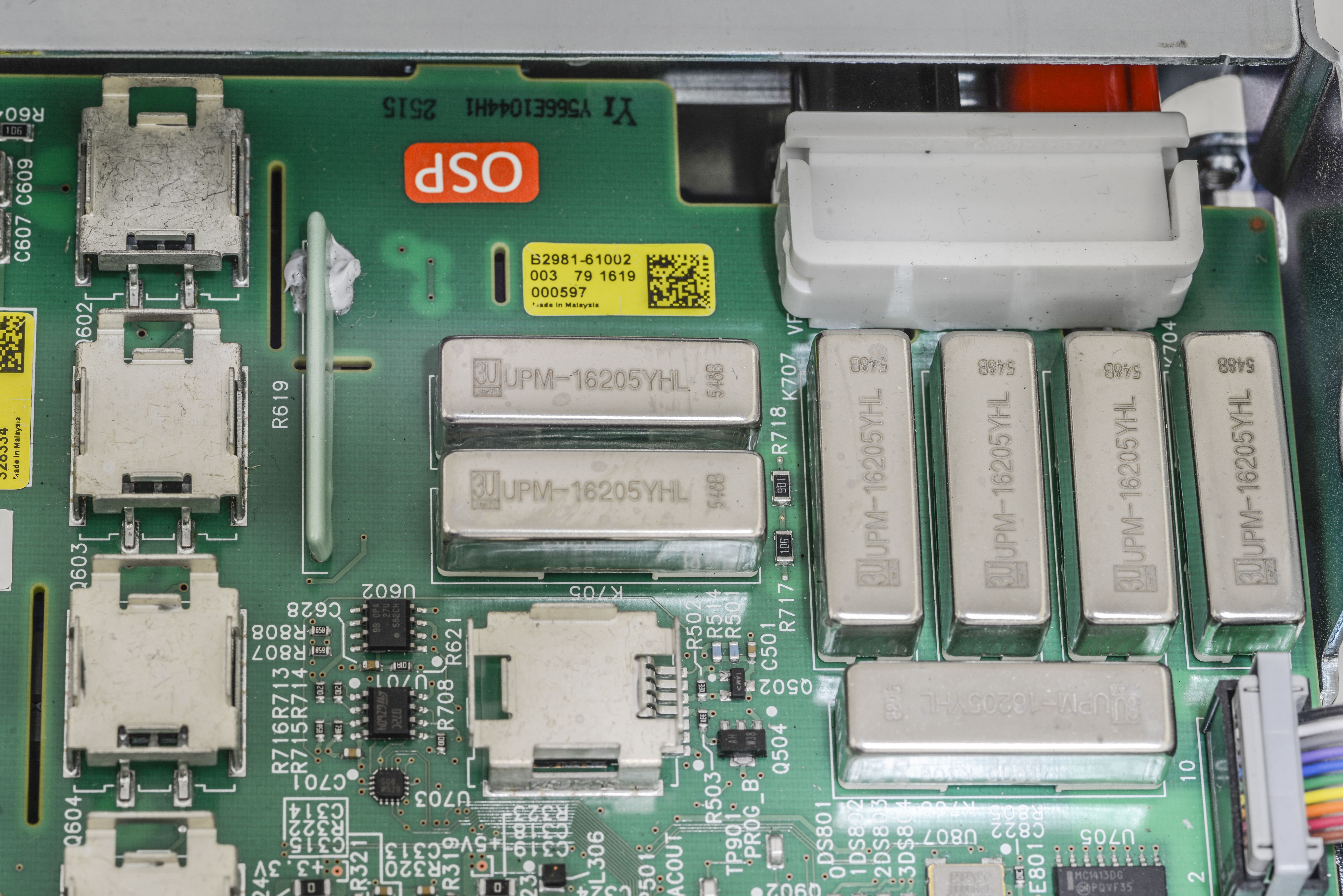
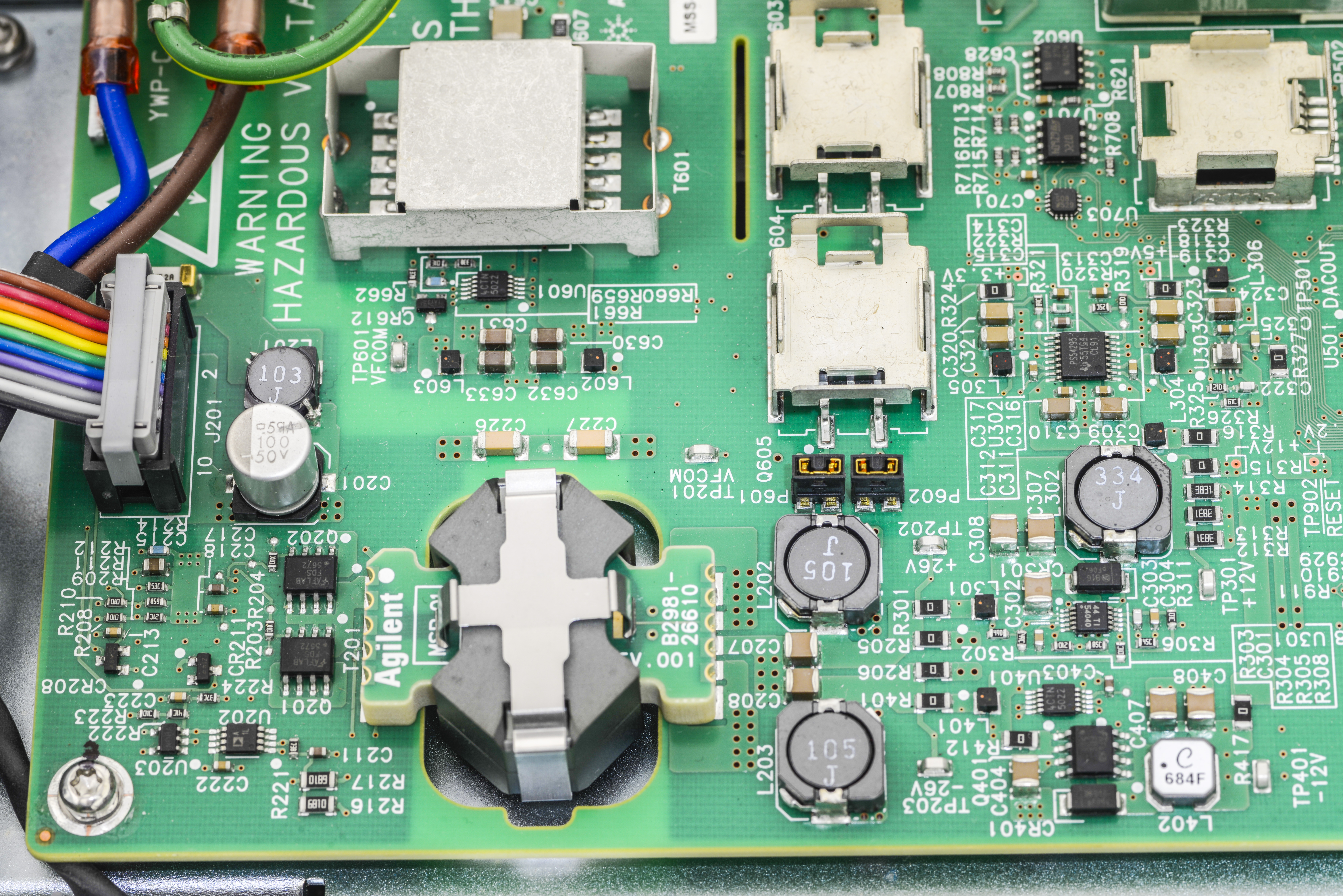
Image : test
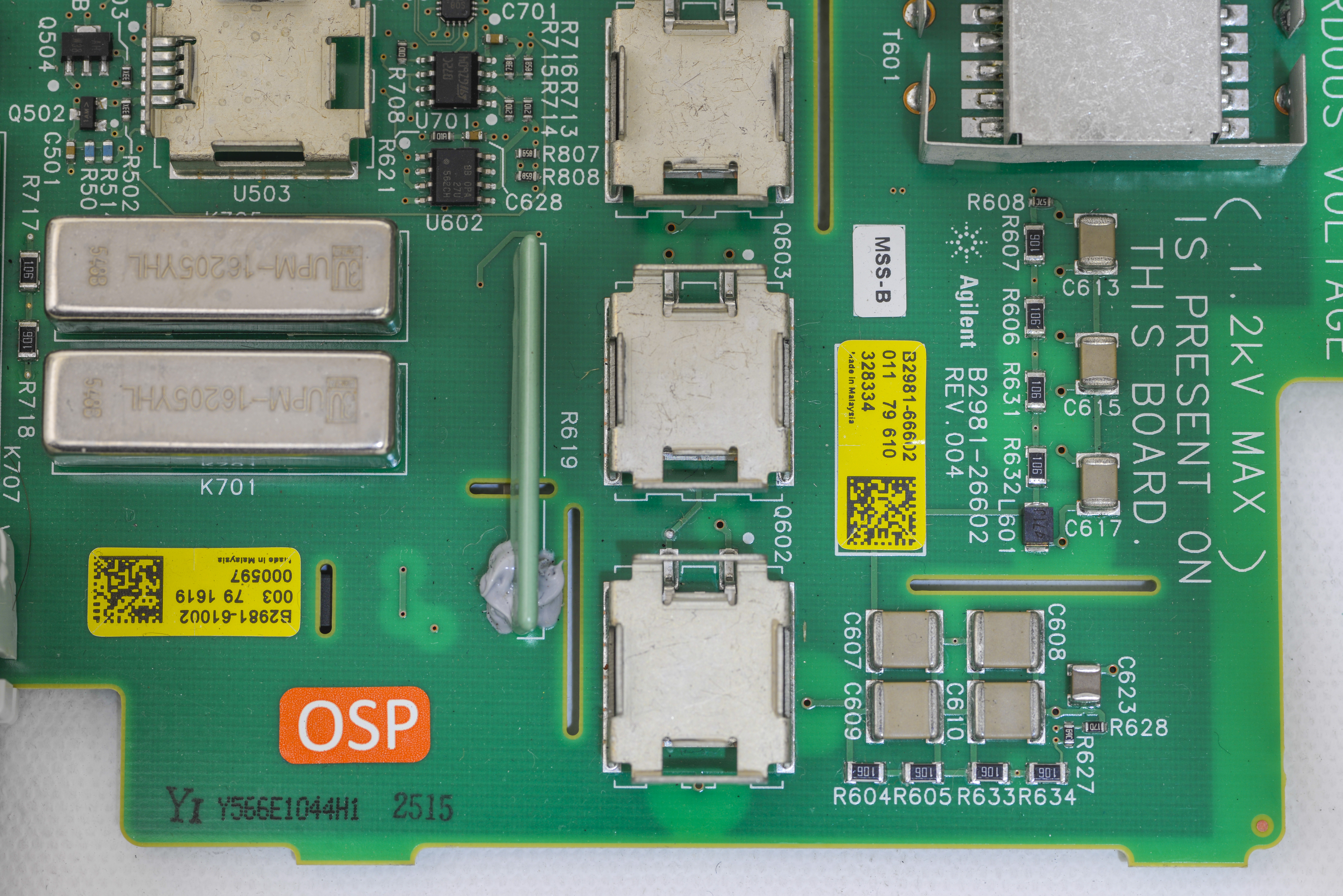
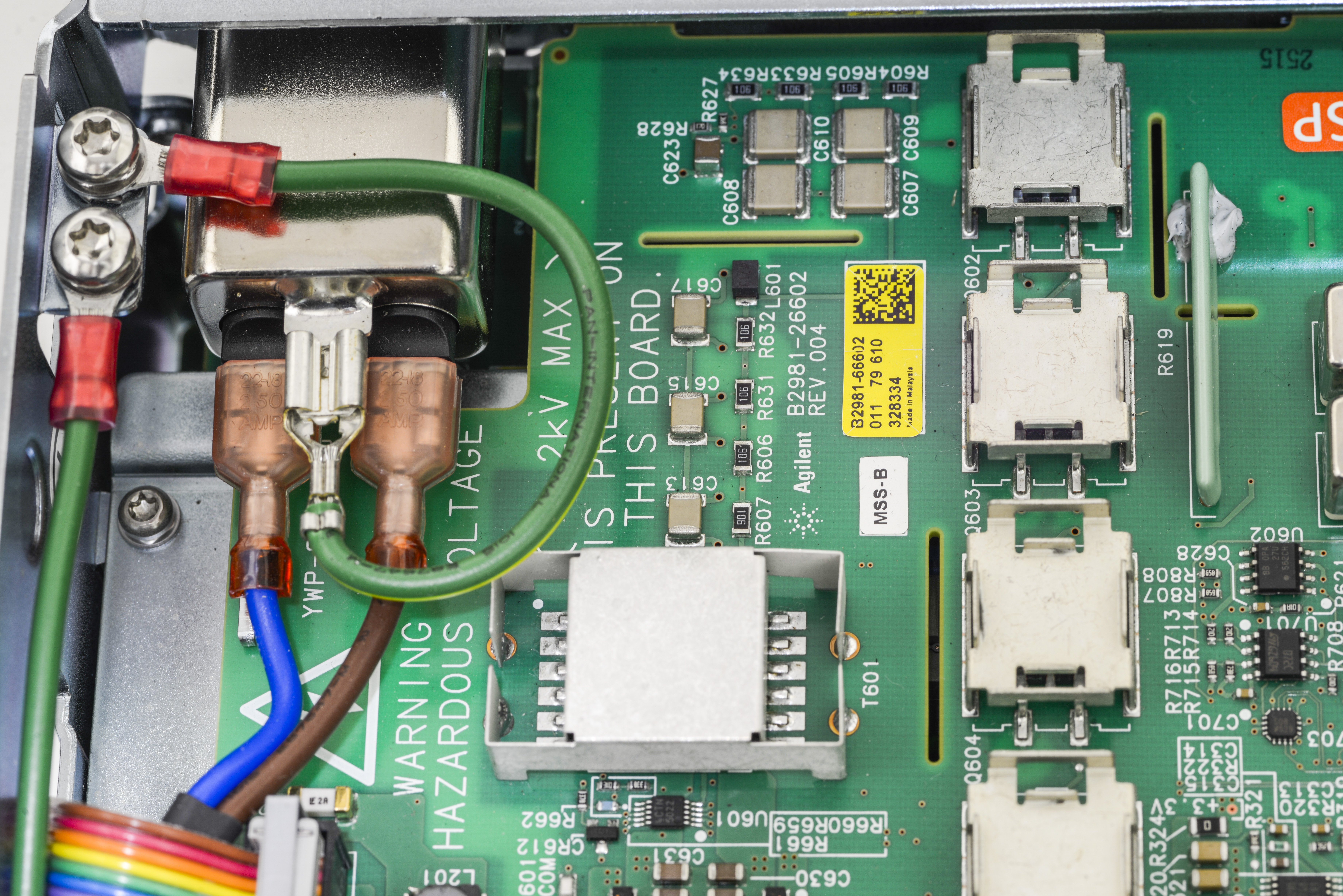
Image : test
Pretty looking magnetic device is custom planar transformer. They got name from planar design made of metal windings etched in multilayer PCB and coupled magnetic core thru machined slots. This construction type of magnetics and conductors assembly have some clear advantages (and drawbacks too) over traditional wire-wound transformers. Advantages are compact footprint with low-height, low leakage inductance and excellent thermal characteristics. Drawbacks are capacitive coupling and more expensive manufacturing and design evaluation, however all these factors can vary a lot depending on application requirements and design.
This is still actively developed field as modern electronics demands even higher power density and better efficiency. There is interesting PhD thesis paper by Ziwei Ouyang on these devices type. Worthy read if you into DC/DC converters and power conversion design.
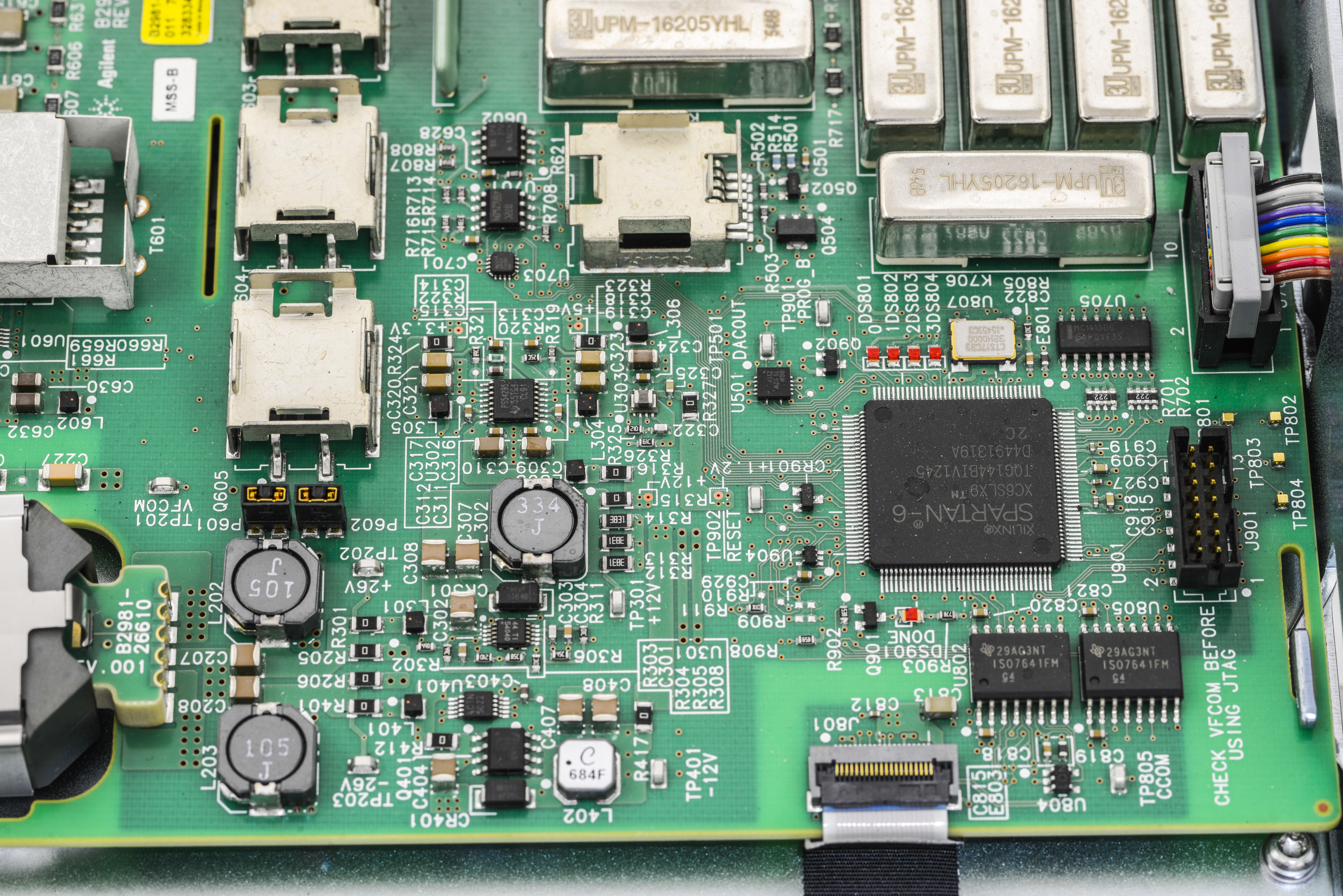
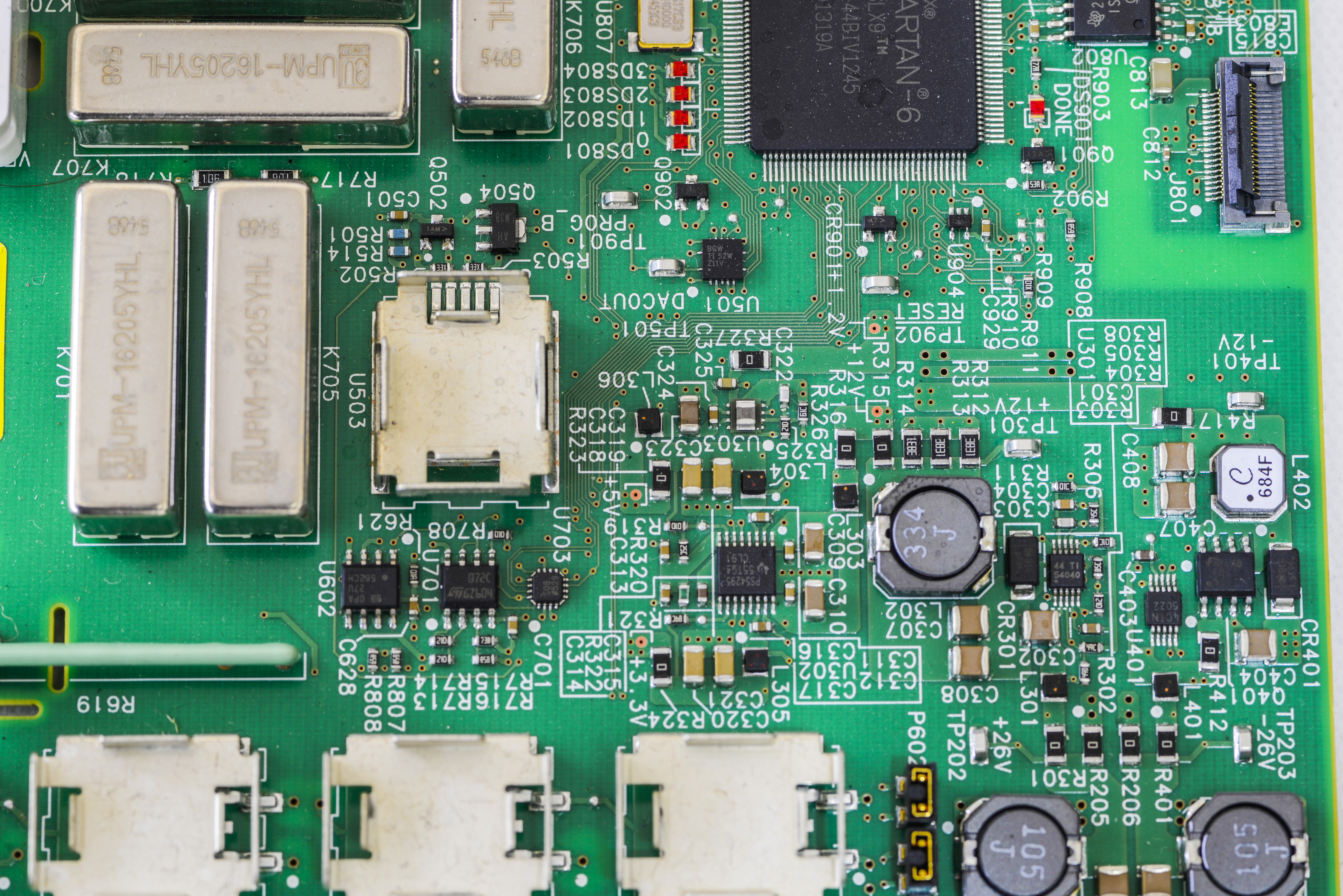
Image : test
This board also have FPGA, Xilinx Spartan-6 LX, XC6SLX9. Used version have 9k logic elements, over 600 Kb of integrated memory, 16 DSP blocks and feature up to 102 configurable I/O pins in used TQFP-144 package.
Tiny QFN-14 chip near DACOUT as you may have guessed already is Texas Instruments DAC8832 voltage programming DAC. This model is low-noise 16-bit voltage output single-channel DAC, operating from external reference. It have good INL (1 LSB) and fast settling time about 1 µs, which is important for fast response. It is connected directly to FPGA I/O for fast interfacing.
Texas Instruments TPS54040 next to L304 33nH inductor is 42V 0.5A step-down buck regulator with adjustable switching frequency. Larger TSSOP package is another TI part – TPS54295. Another synchronous step-down buck switcher with intergrated FET and two output channels. Inductors next to this regulator are tiny, almost same size as 0805 passive component package, but wider.
U303 catch the eye too, it looks like tiny 8-pin DFN package but with 0805-size capacitor on top. It has to be some local LDO regulator.
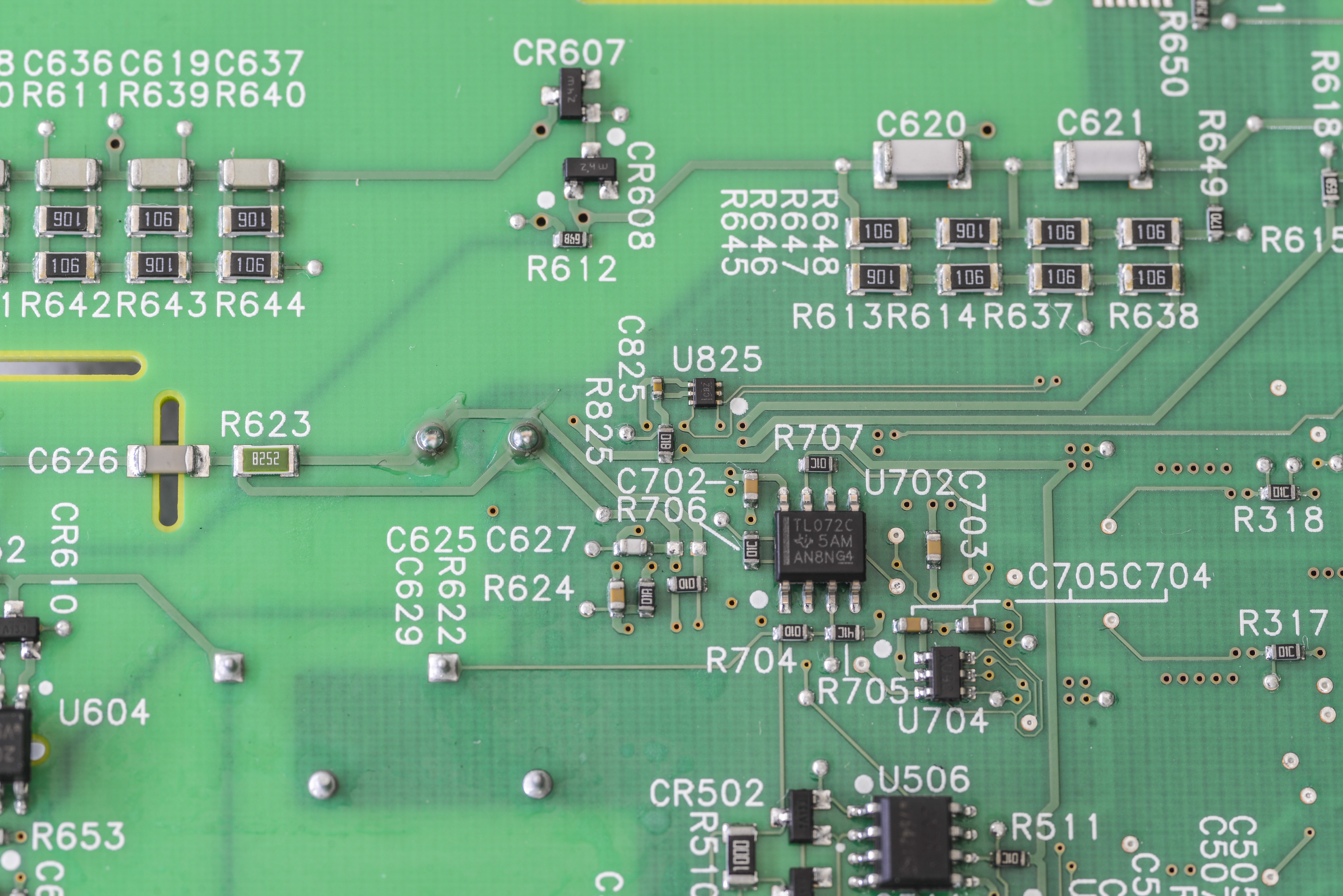
Image : test
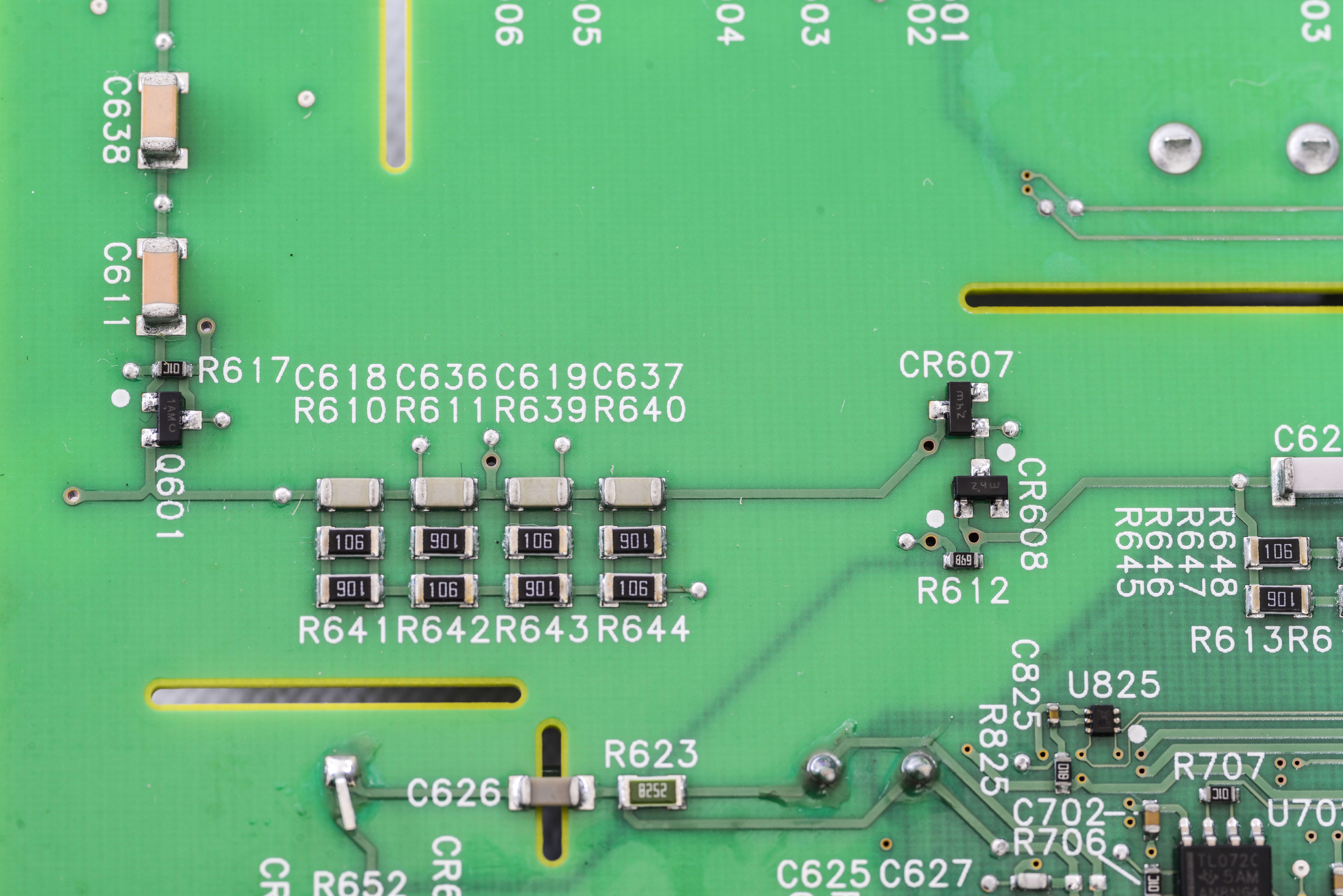
Image : test
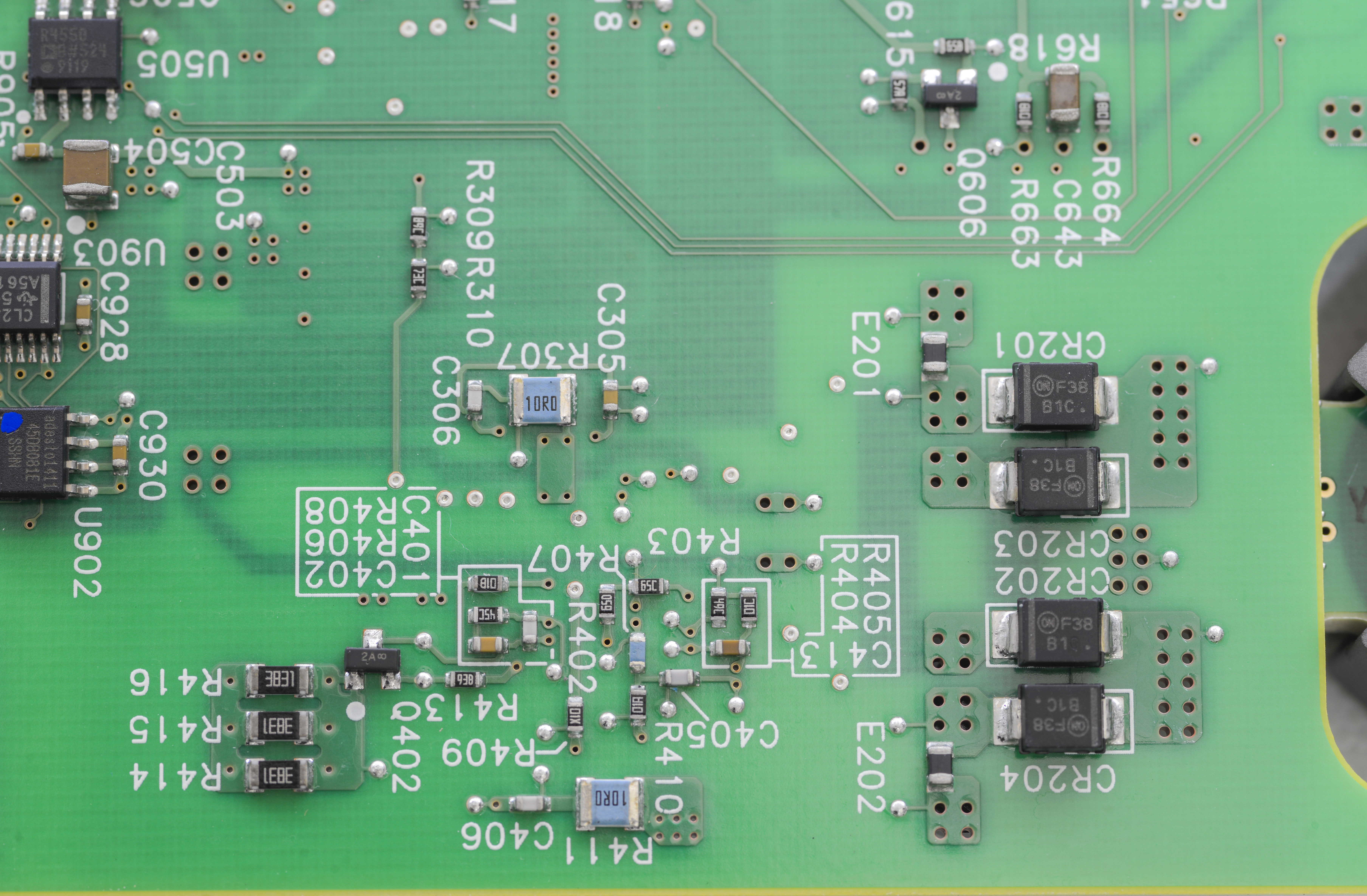
Image : test
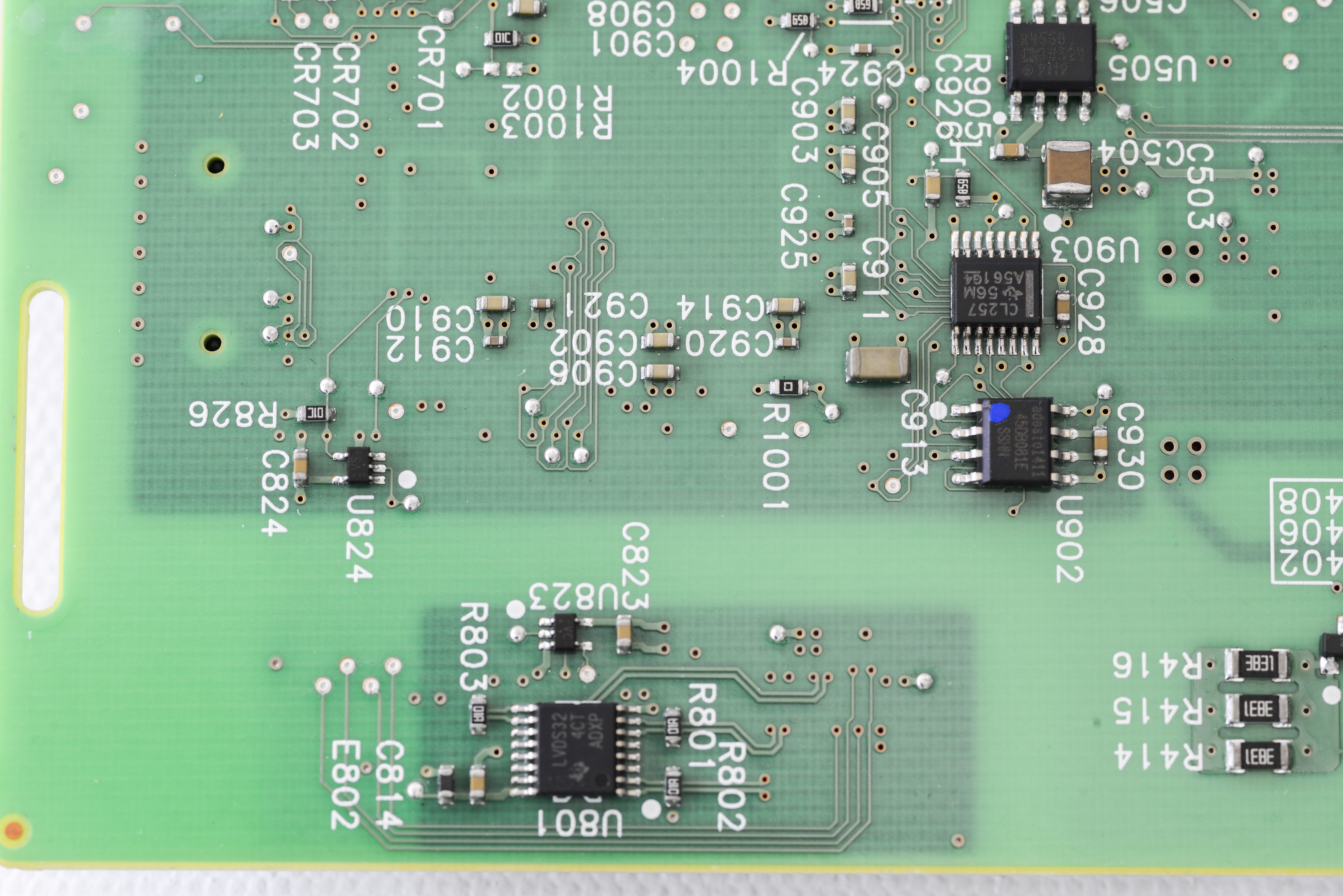
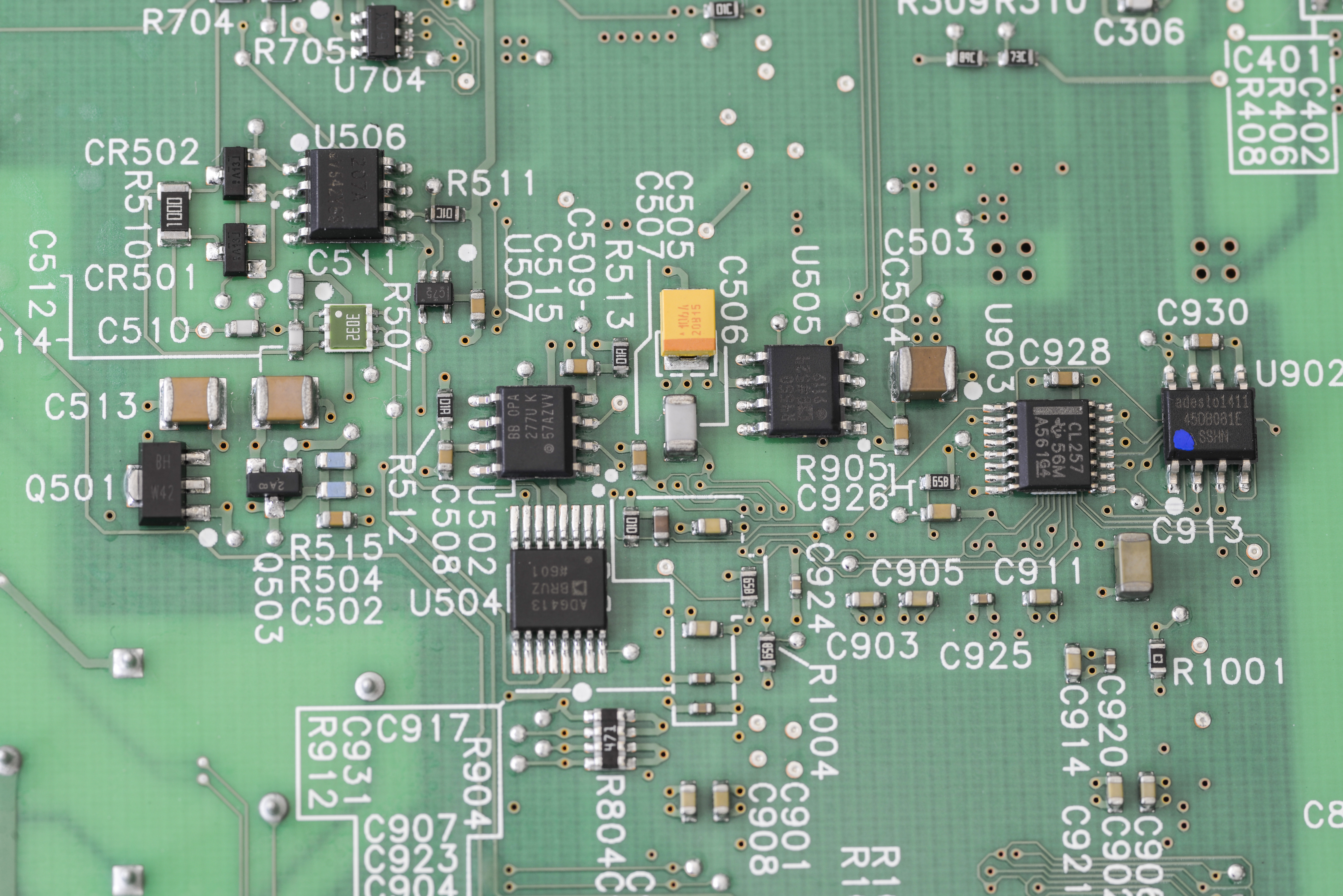
Image : test
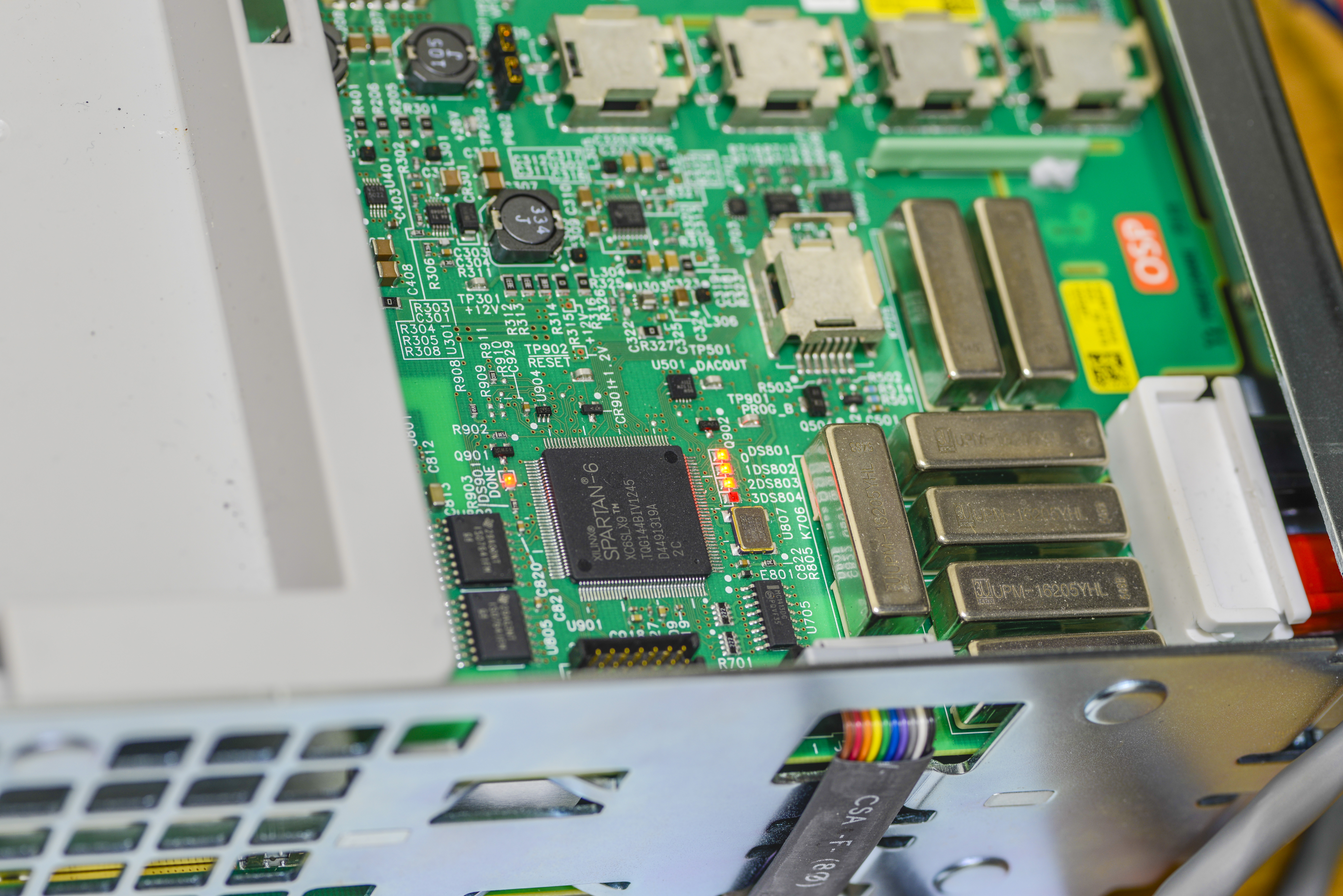
Image : test
Analog front-end assembly B2985-61101
Now it’s time for the heart of the electrometer, main analog front-end and acquisition board, located on bottom of the meter.
This is fragile and sensitive assembly. Removing shielded cans and components exposure to dust will null and void unit calibration and may affect performance of the instrument. Do NOT do this, unless you agree with expensive repair and recalibration service.
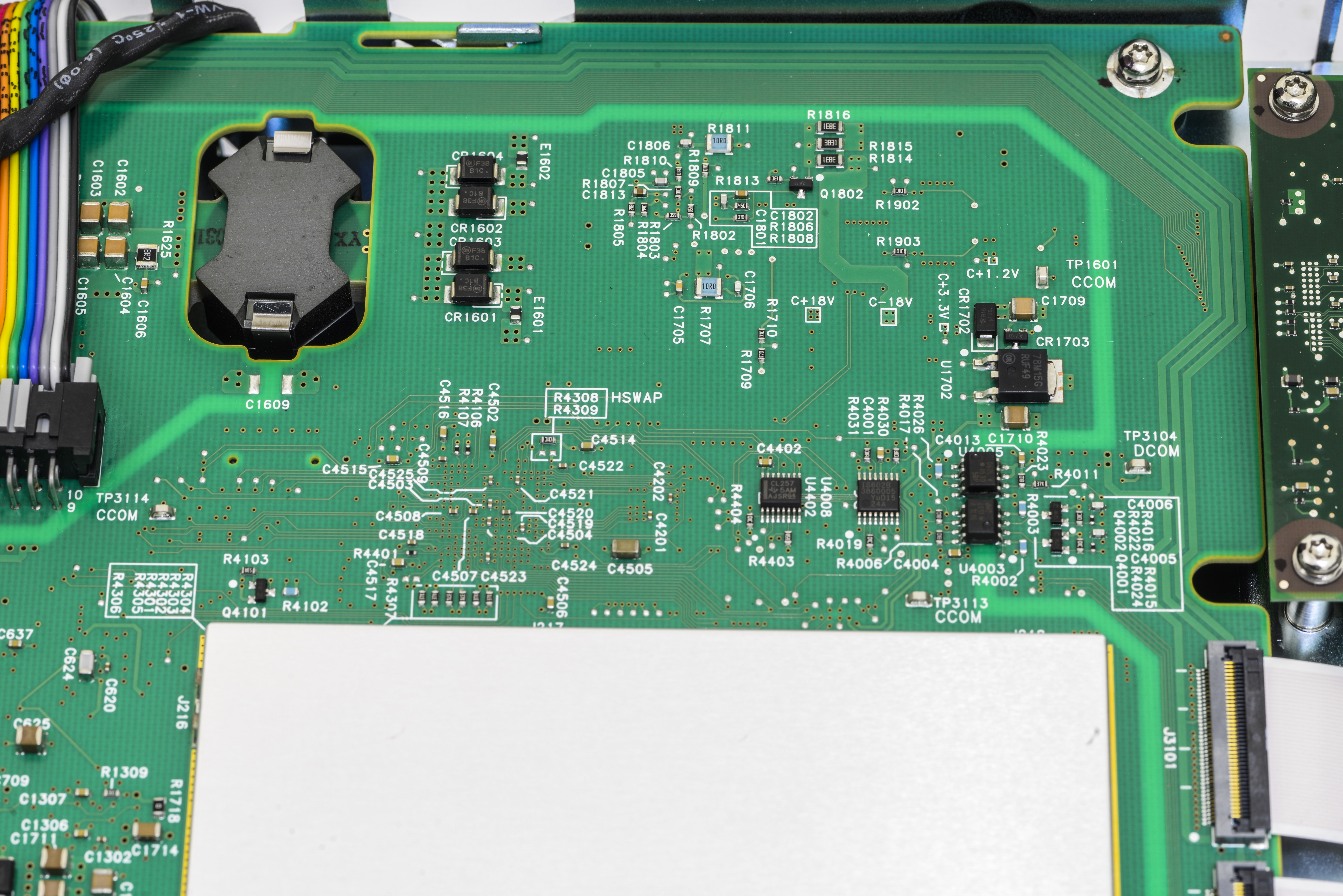

Image : test
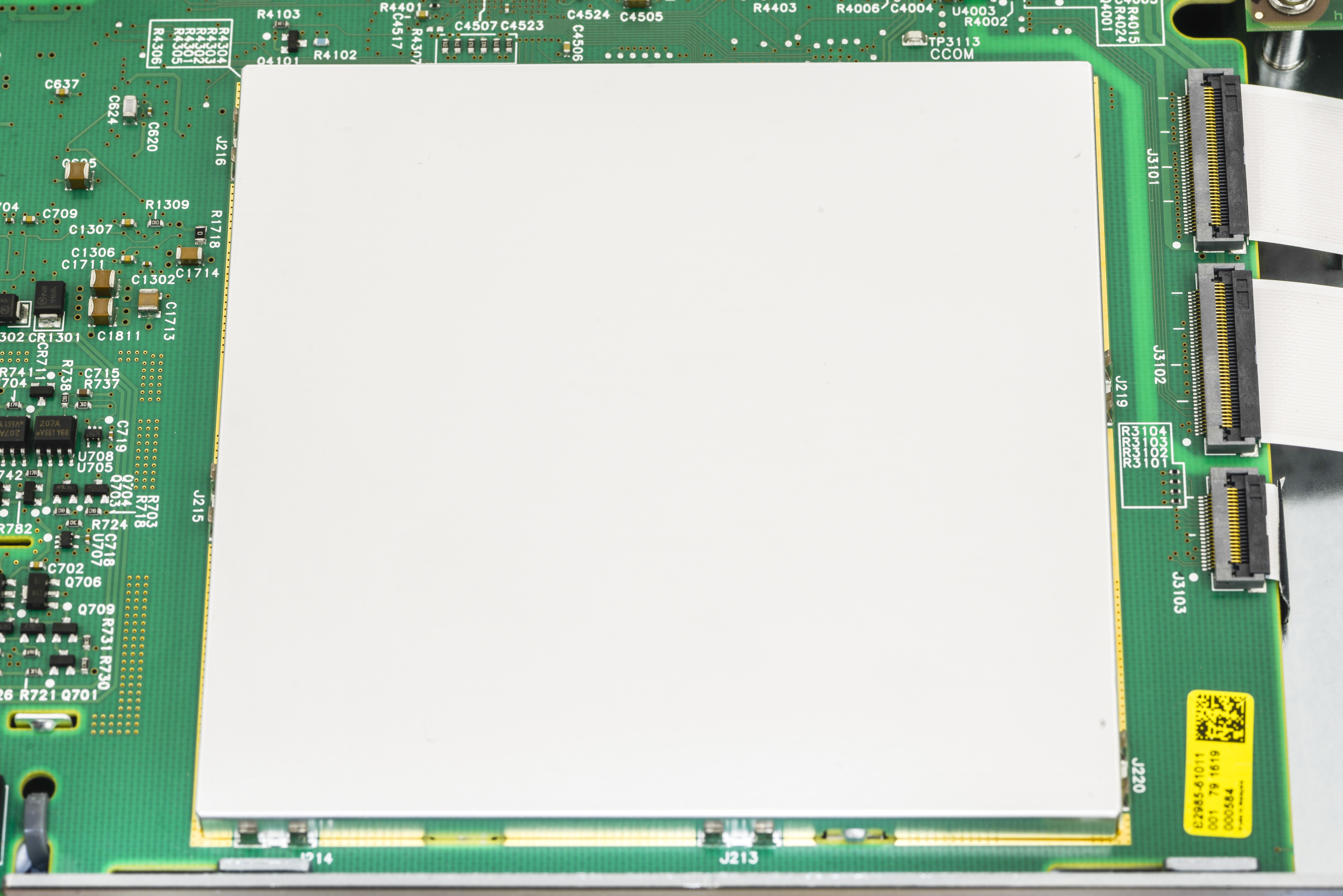
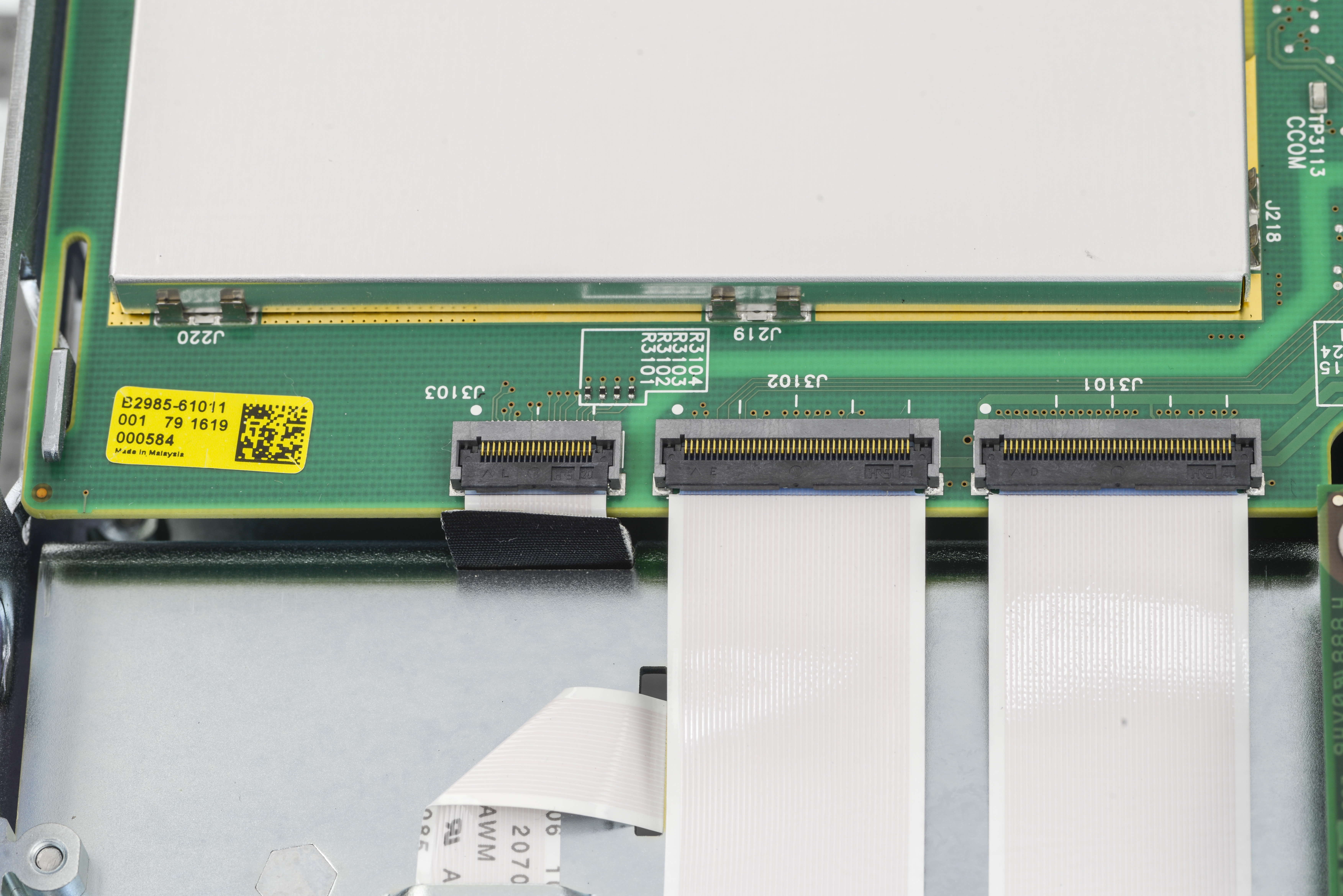
Image : test
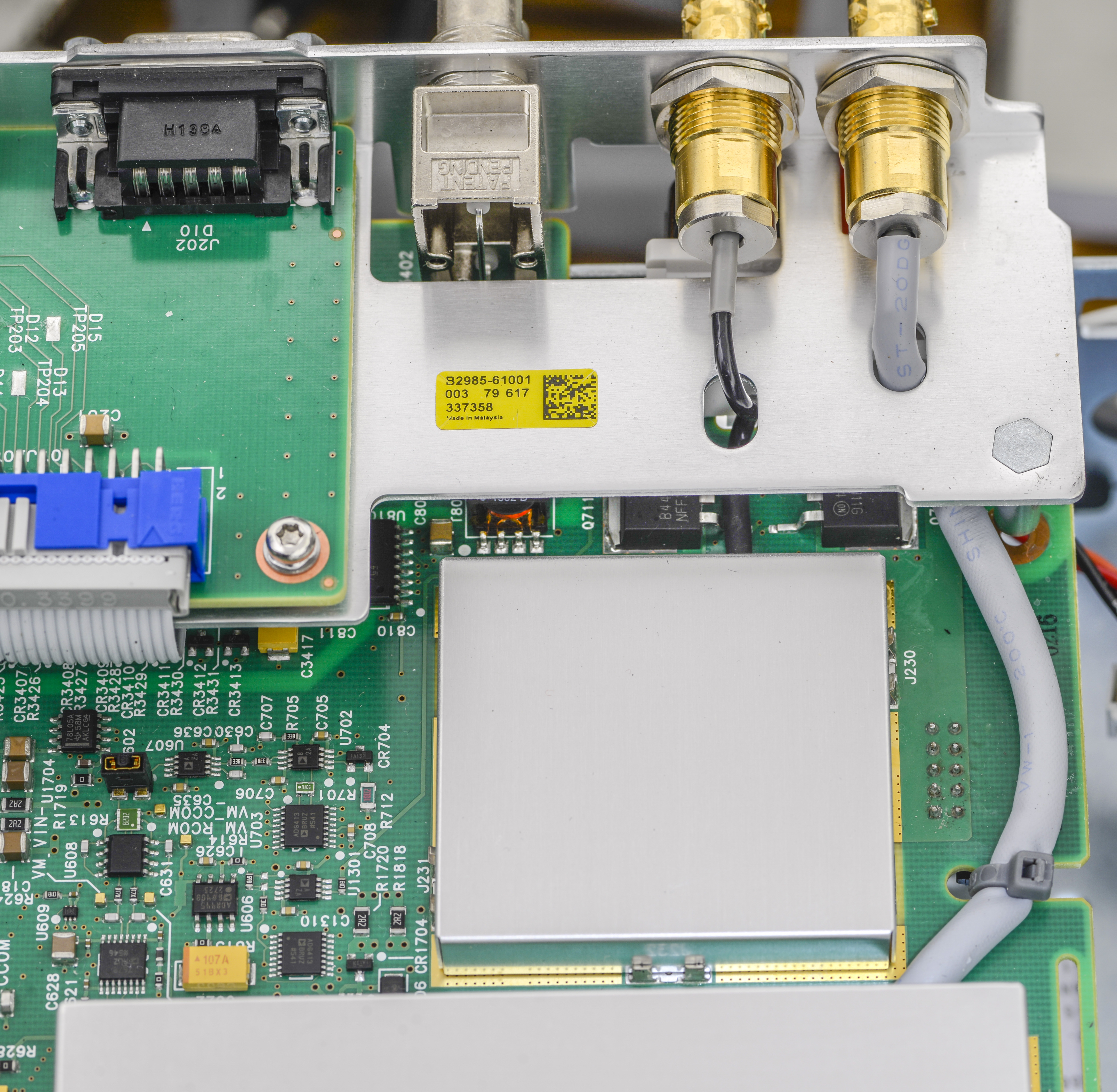
Image : test
Insulator such as a cable jacket or board dielectric is always physically existent between the current input terminal of the ammeter and the other voltage potential. When the insulator is biased by a voltage source, a certain level of leakage current can flow in the insulator and generates a measurement error. This issue can be mitigated by using a much higher resistivity material or using a shorter cable to increase the equivalent resistance, but these are sometimes not realistic solutions in practical environments.
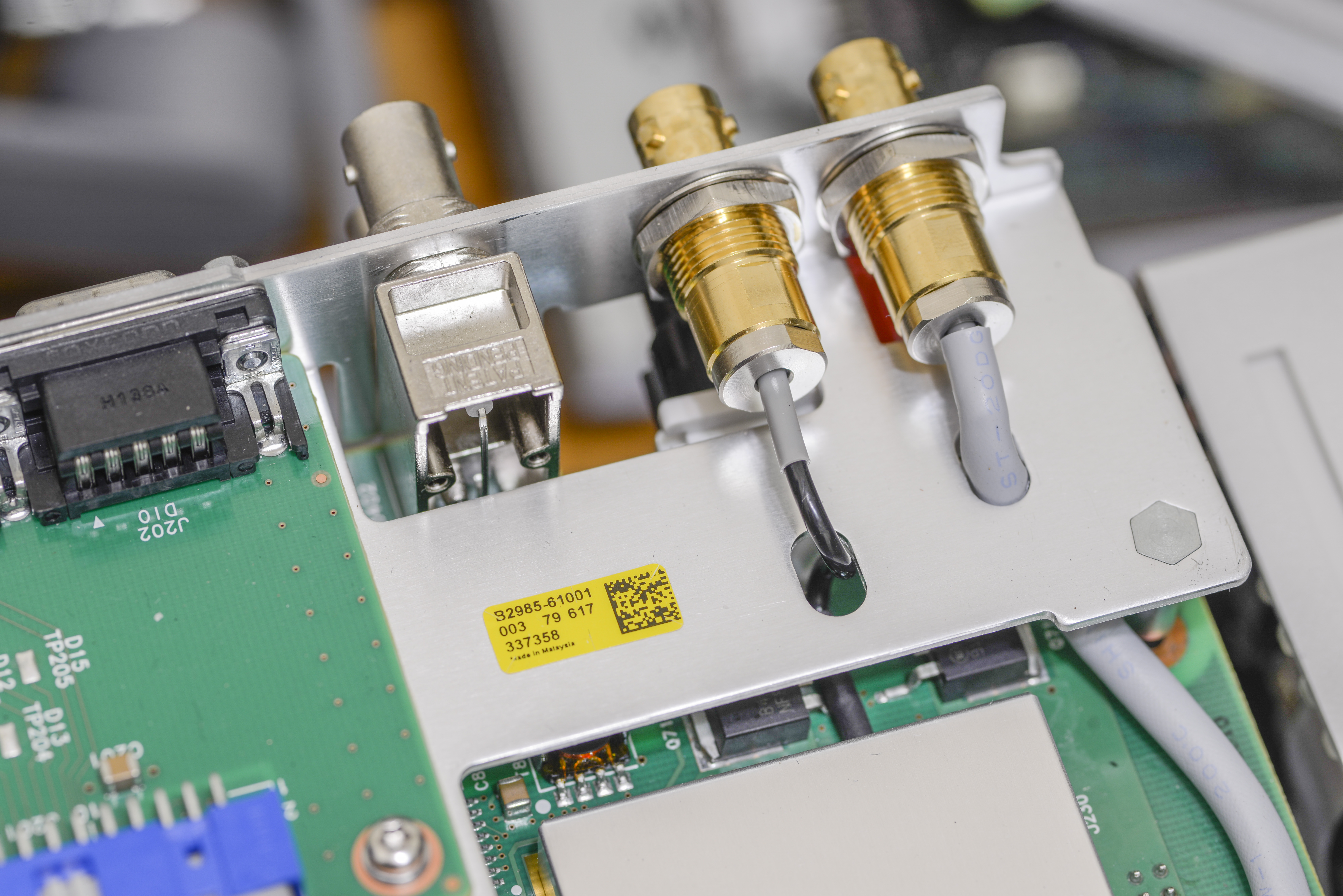
Image : test
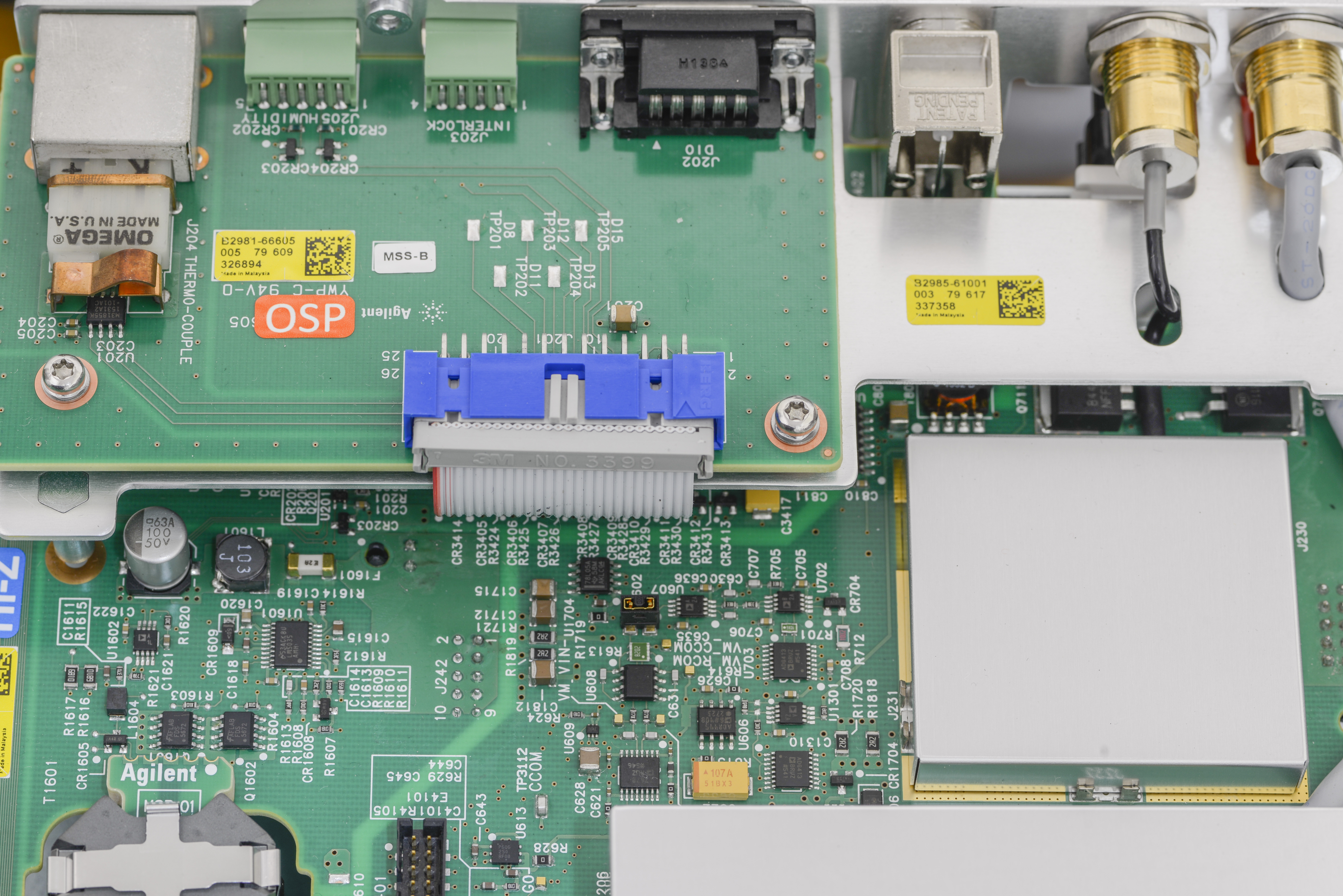
Image : test
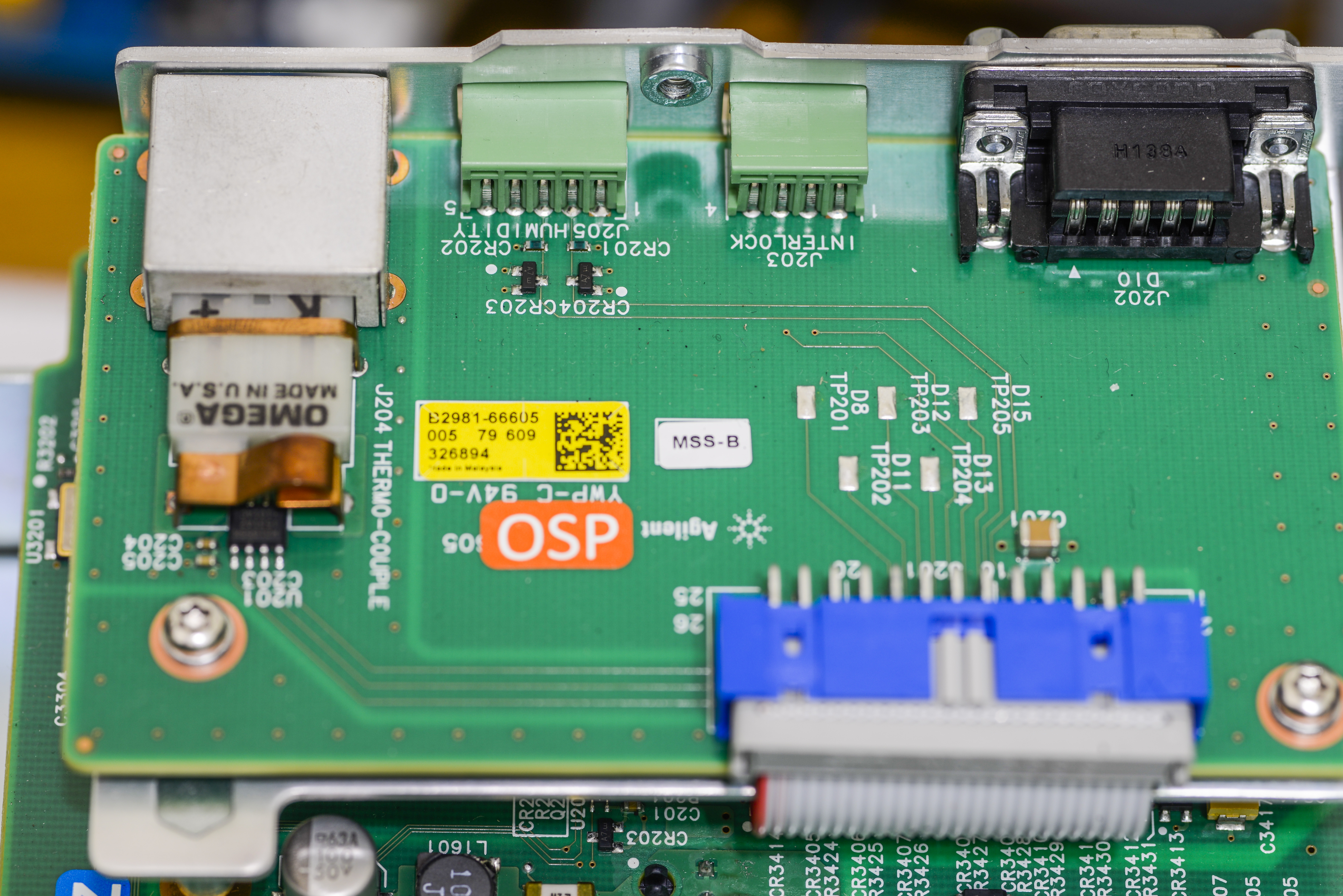

Image : MAX31855 sensor test
Image : test

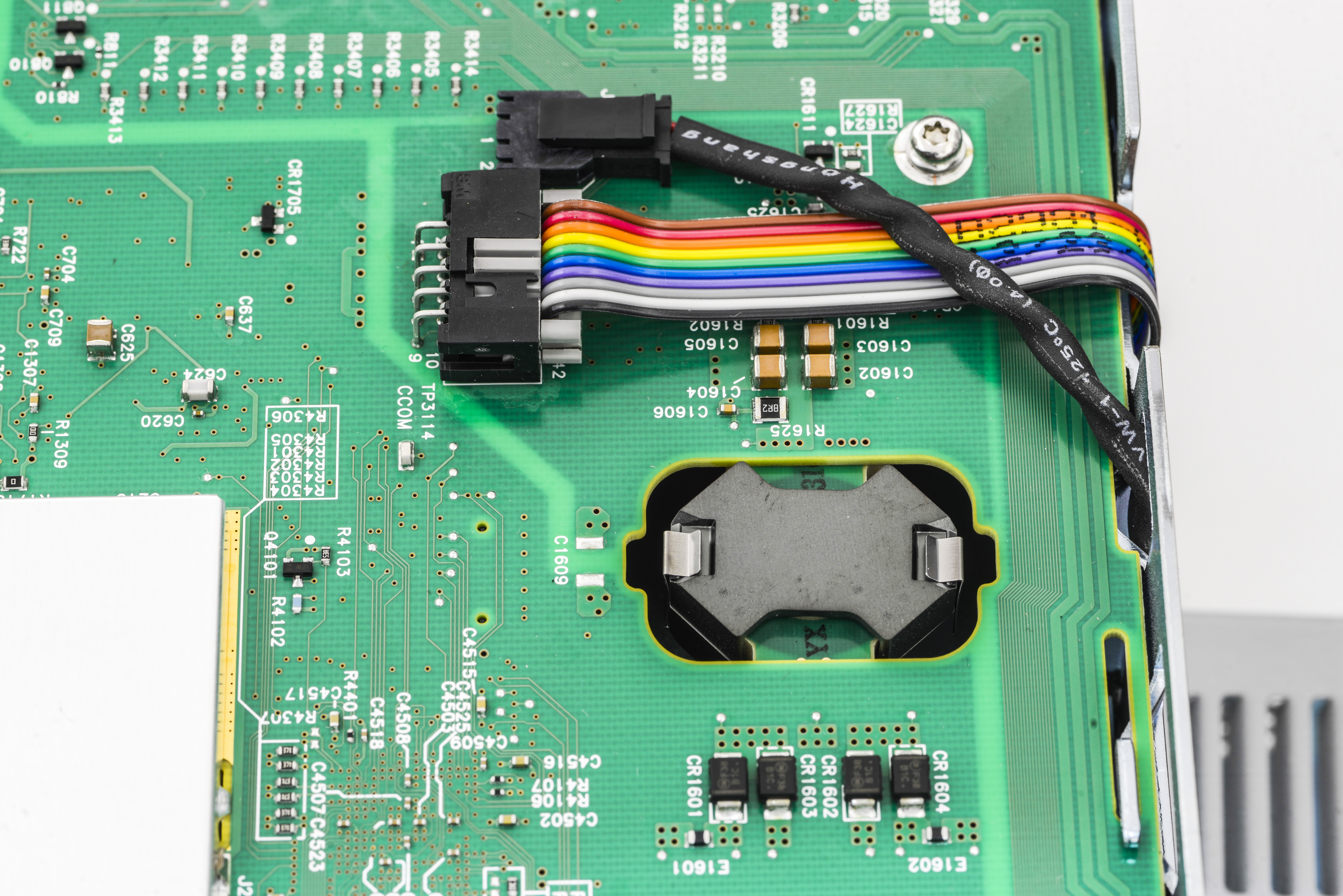
Image : test
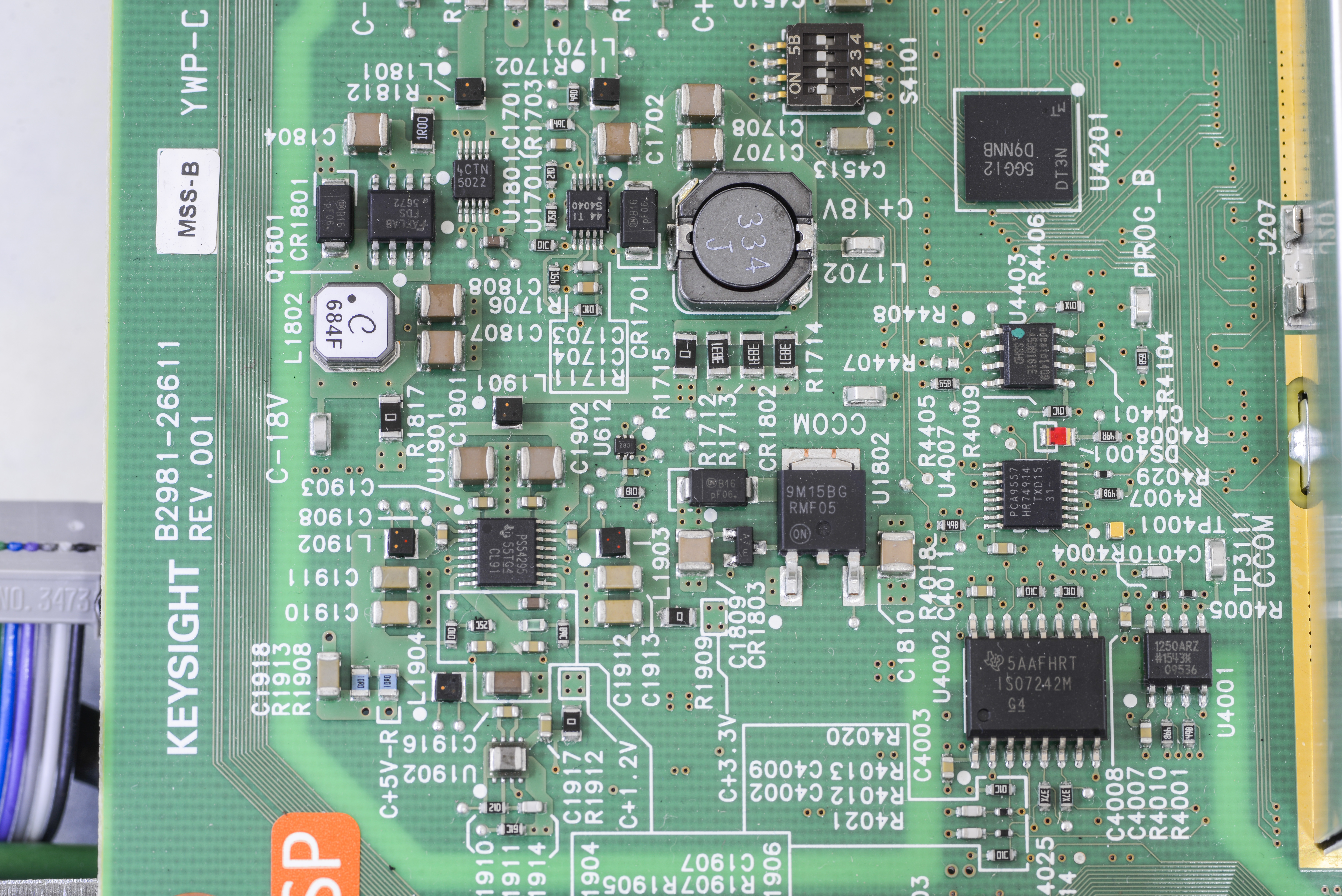
Image : test
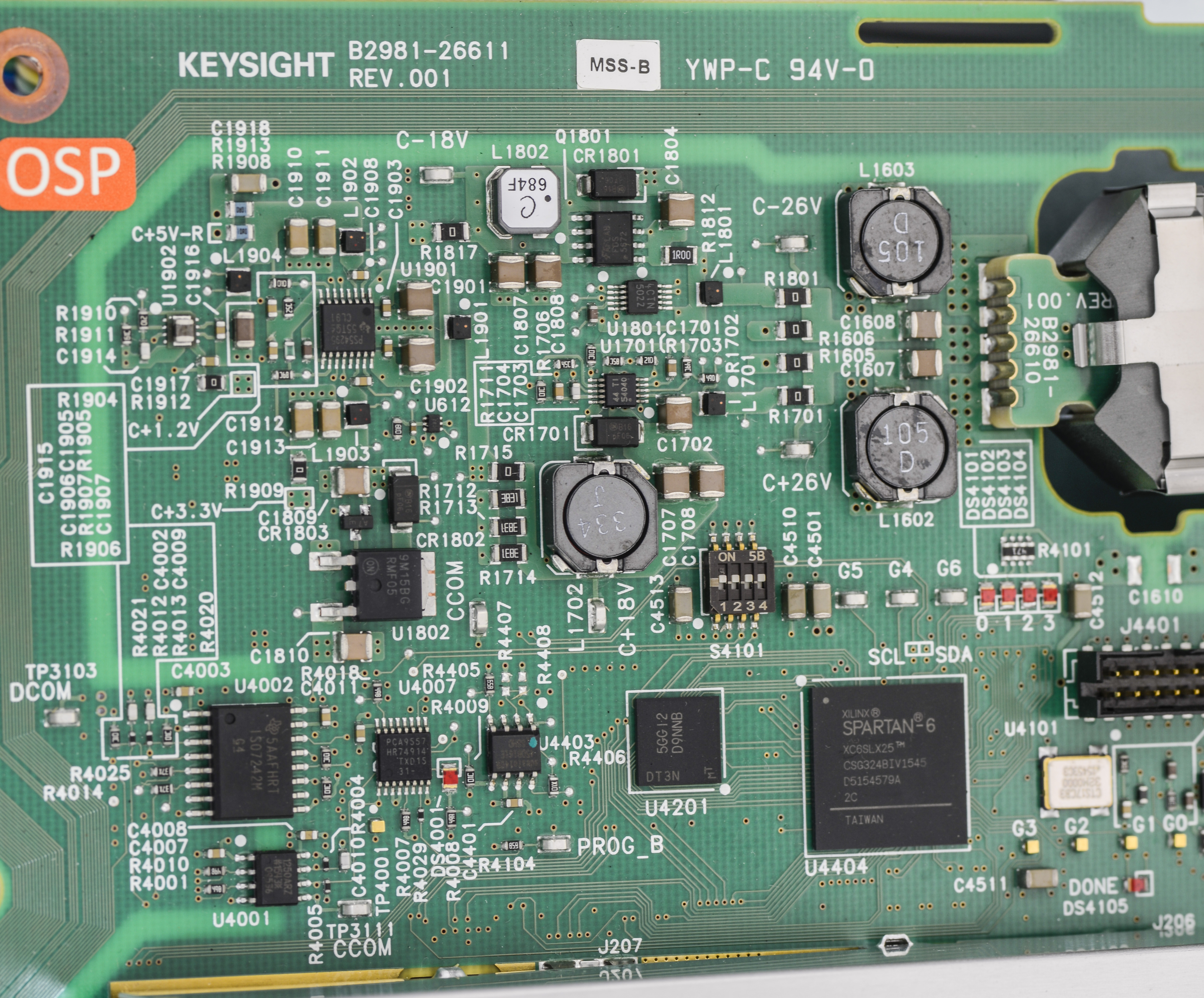
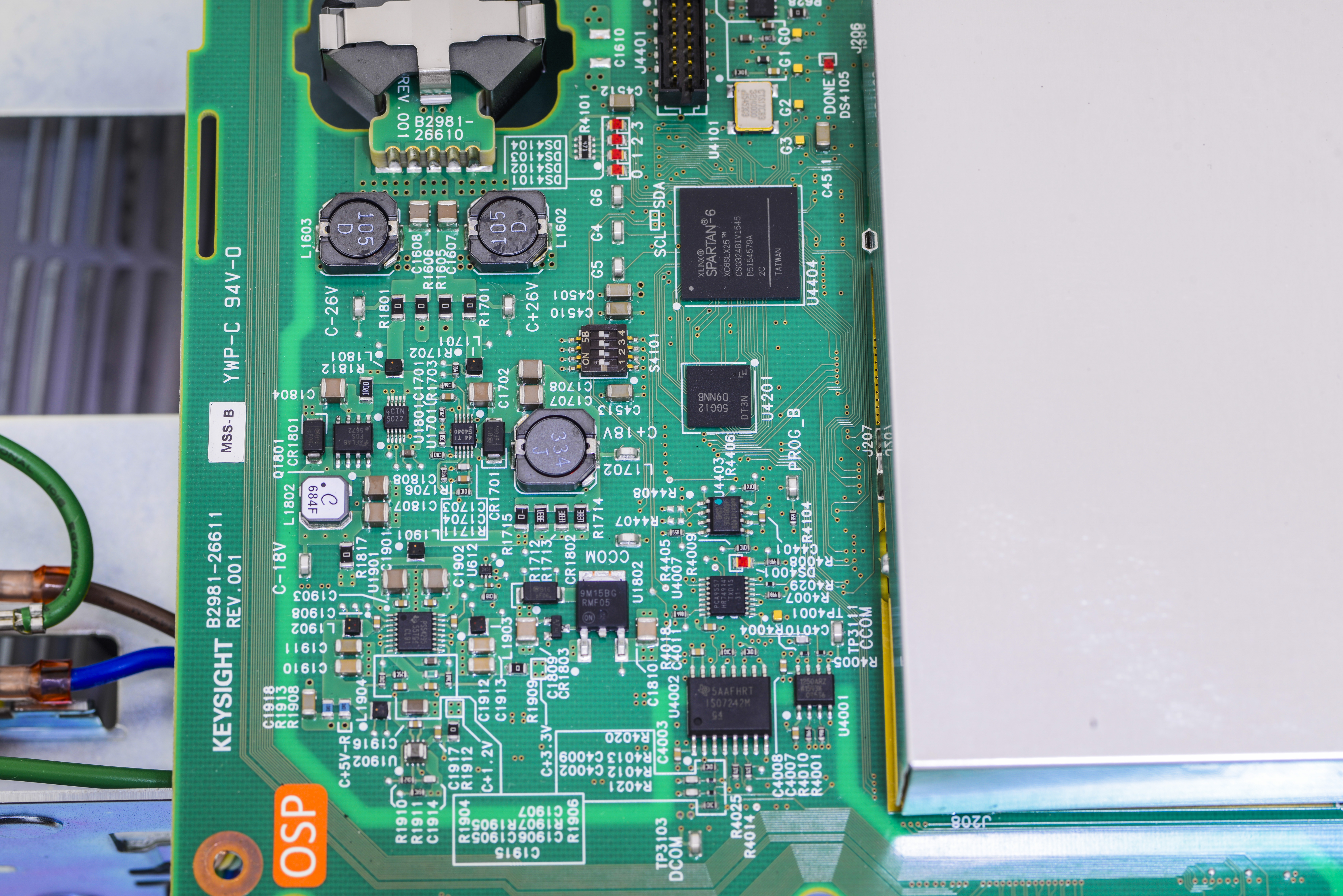
Image : test
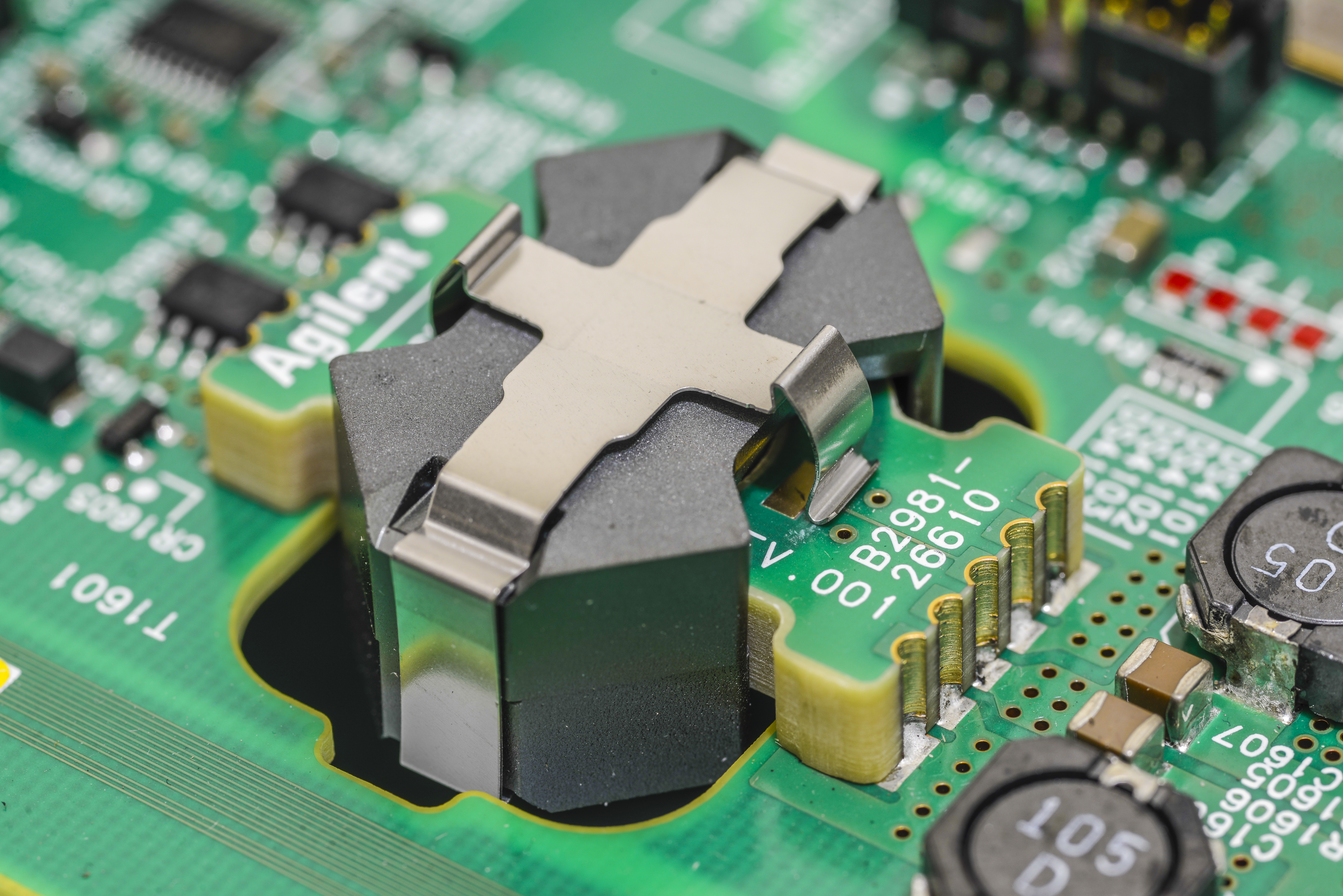
Image : planar transformer
Similar to voltage source board here we can also find another Agilent-designed planar transformer to provide isolated power between different parts of the board.
Now time to remove shields and reveal the secrets.
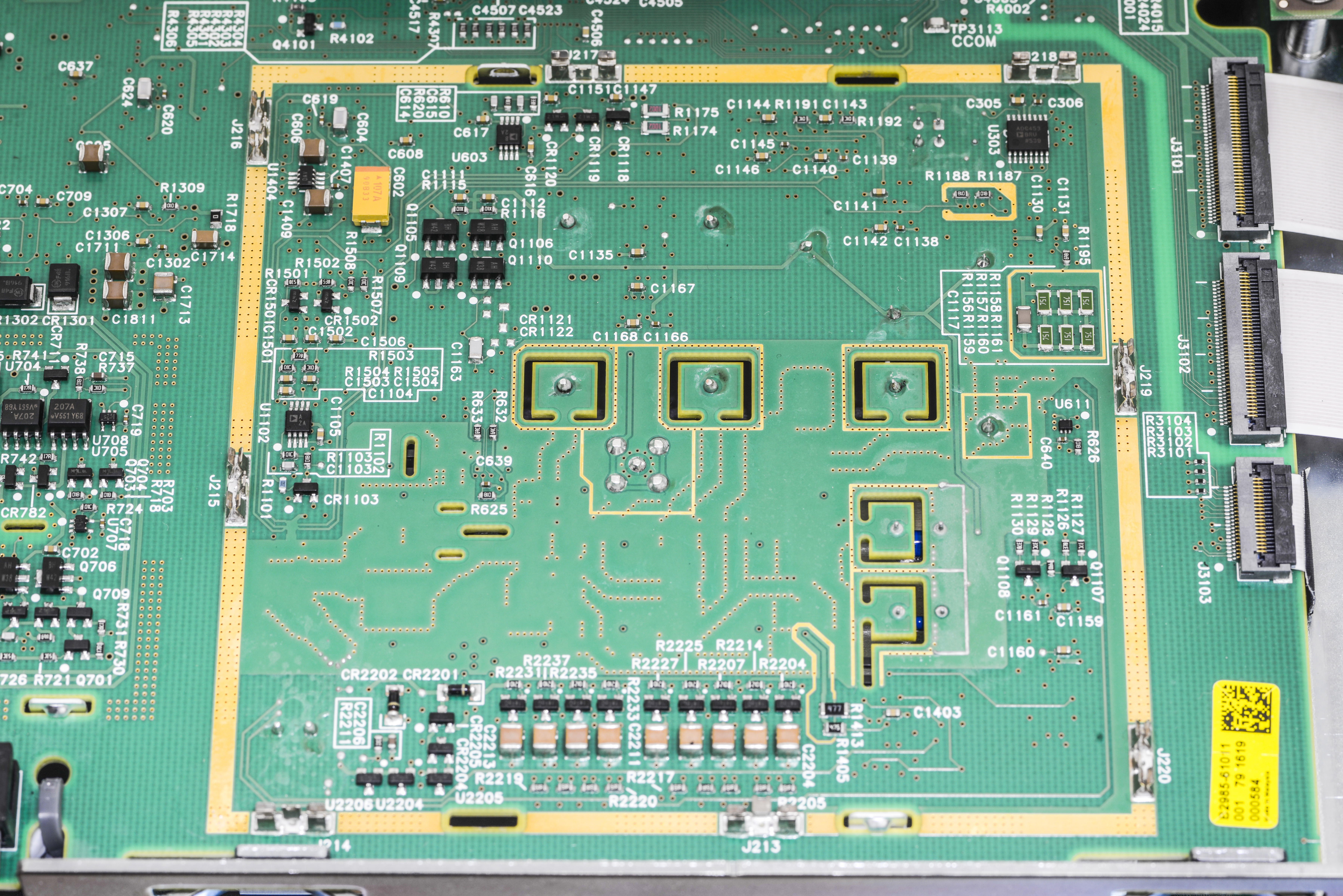
Image : test
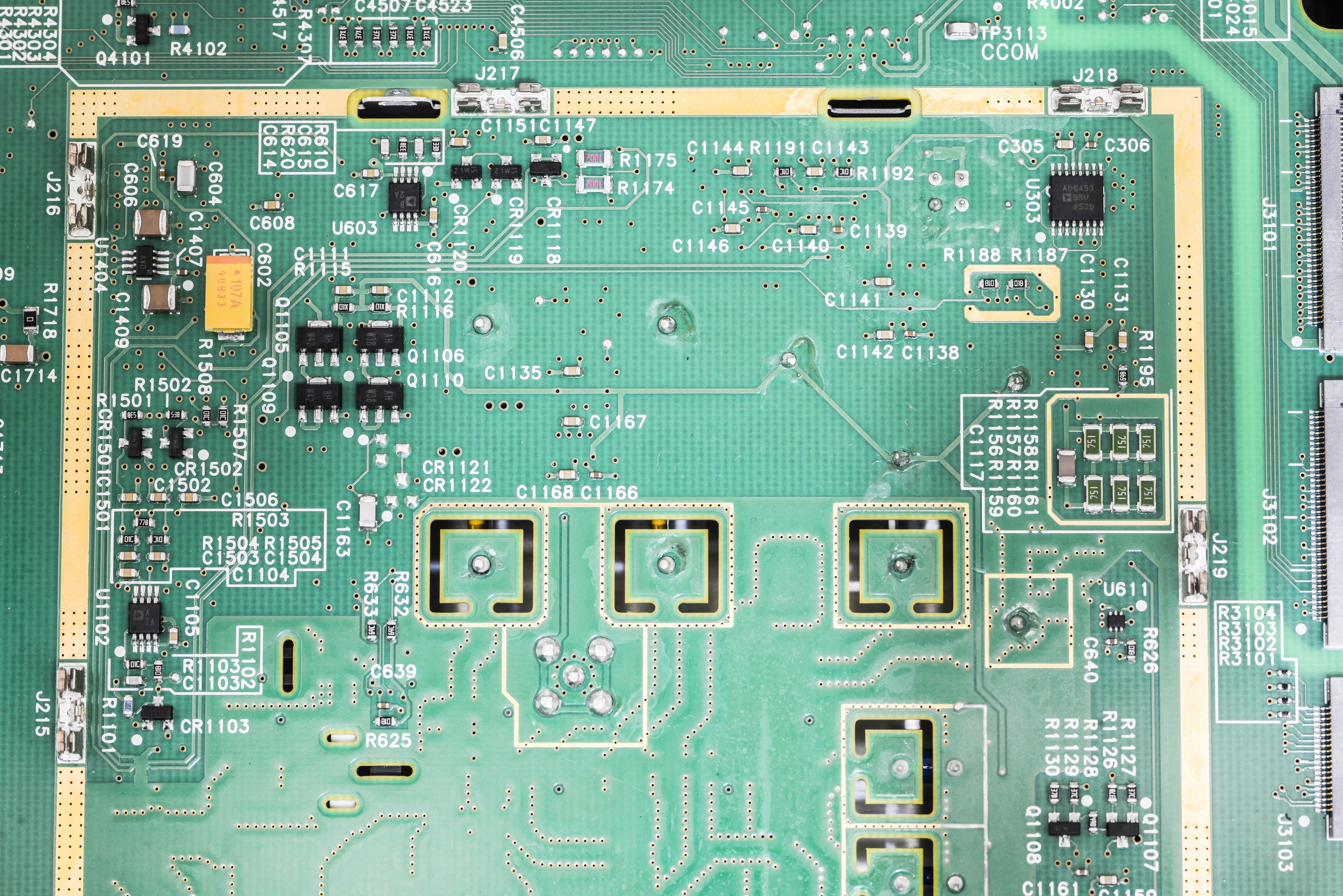
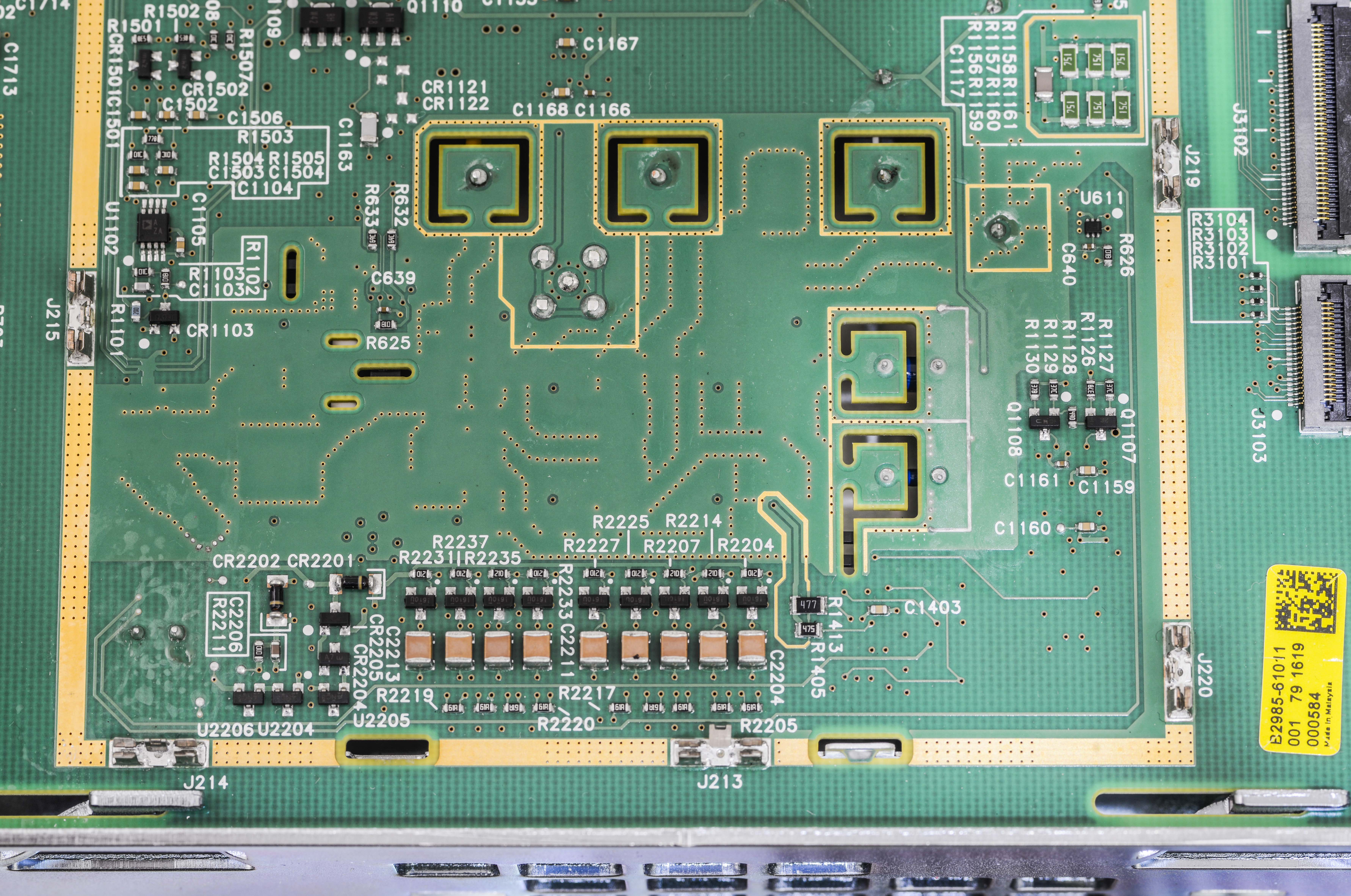
Image : test
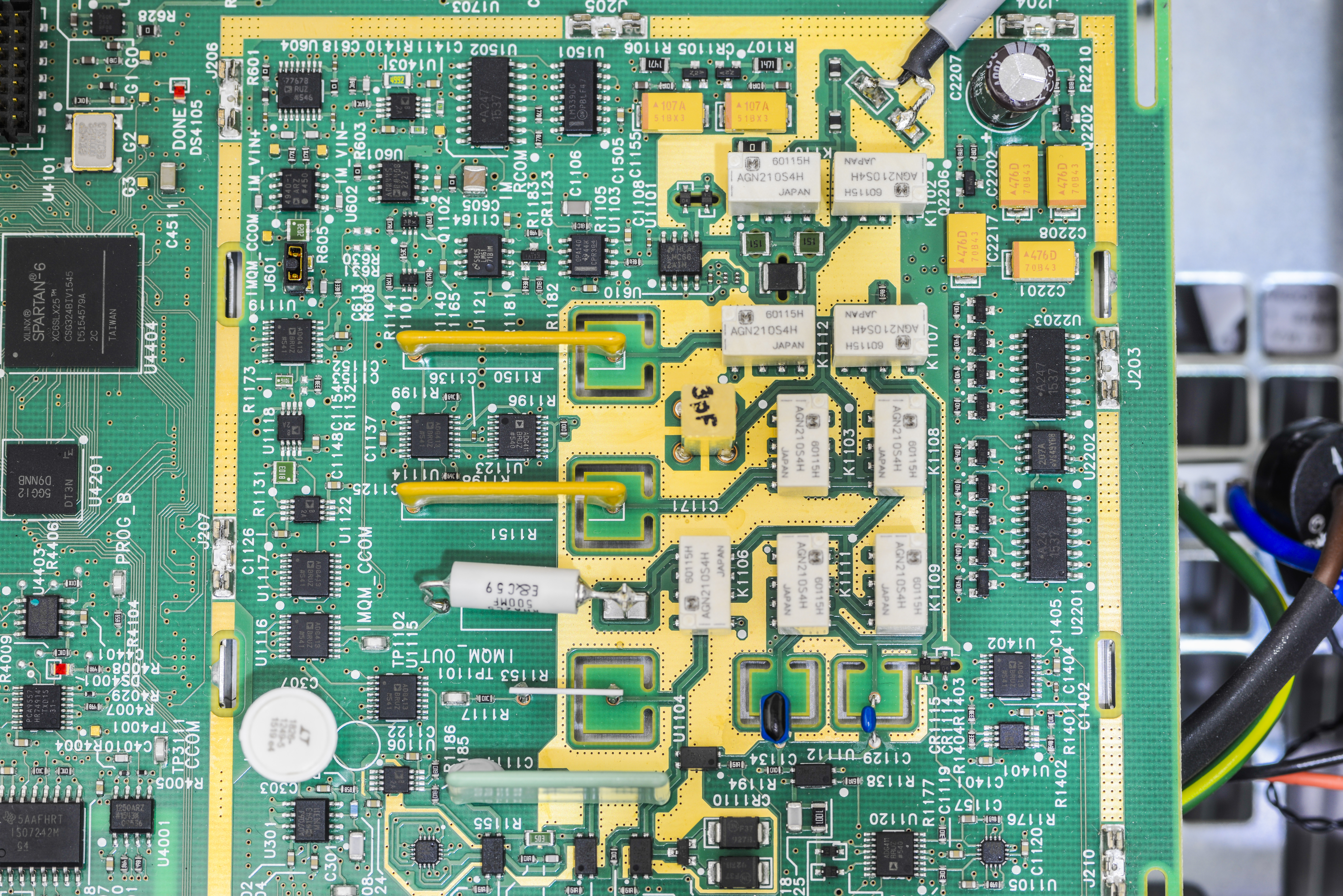
Image : test
Image : test
Main voltage reference is typical LM399, selected by Keysight for their specifications. Chip is relabelled with custom Keysight partnumber 1826-1249-5. Reference manufactured around week 19 in 2015.
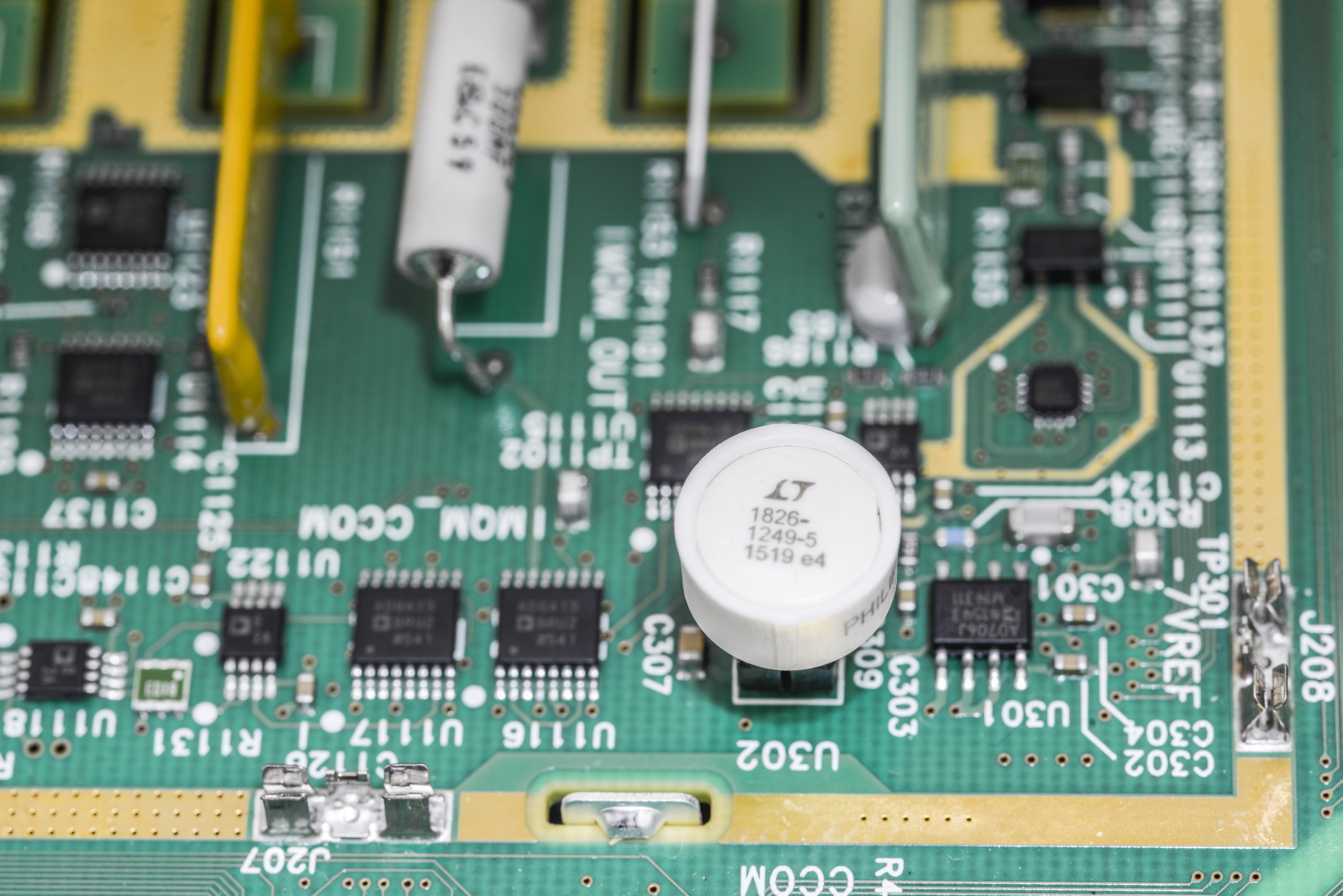
Image : test
It is interesting to see different approach chosen for this instrument, particularly choice of switching relays. Keysight opted for general purpose relays and rely on heavy guarding to prevent excessive leakages, rather than special high-isolation reed relays typical for electrometers and picoammeters. Image below shows front-end area of direct competitor for B2987A unit, which is Keithley 6517A electrometer (modern Model 6517B have updated design but likely to follow same idea).
We have fixed few 6517A before, so there is photograph of it’s front-end for comparison. Keithley opted for LMC6001 as input amplifier. Largest feedback resistors used in Keithley meter are thin-film 4 TΩ and 1 TΩ.

Image 5: Keithley 6517A front-end, using COTO reed relays and custom parts
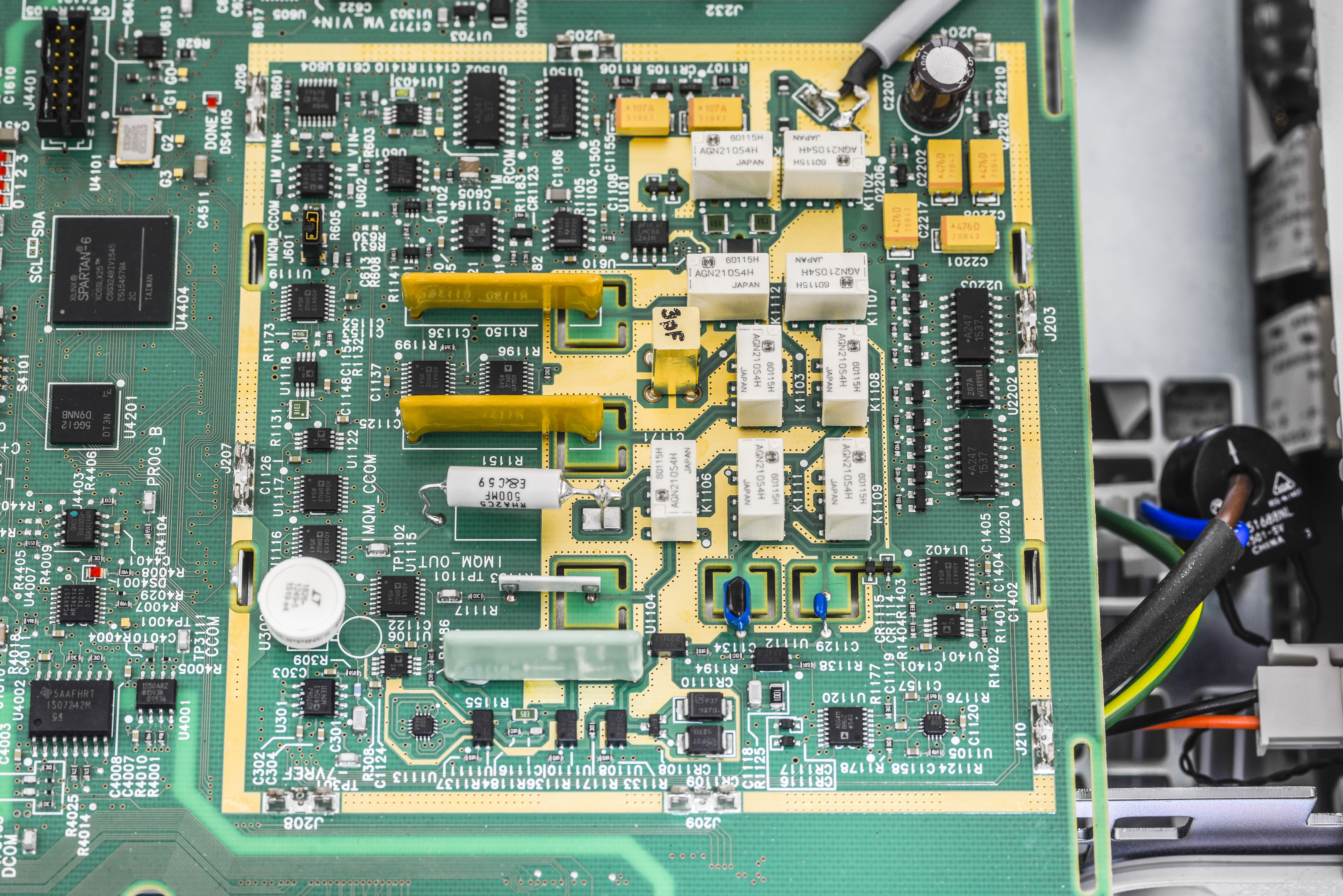
Image : test
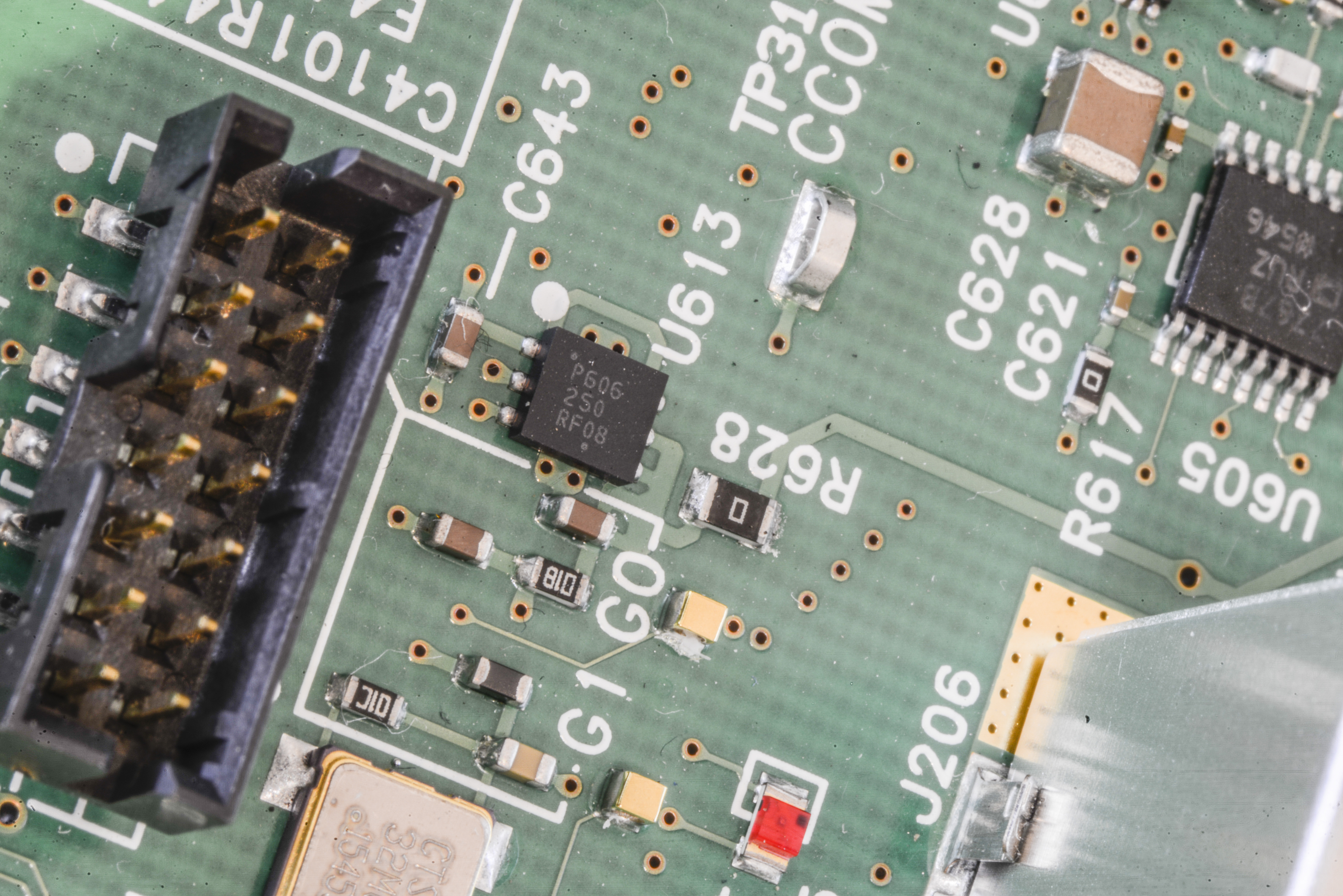
Image : test
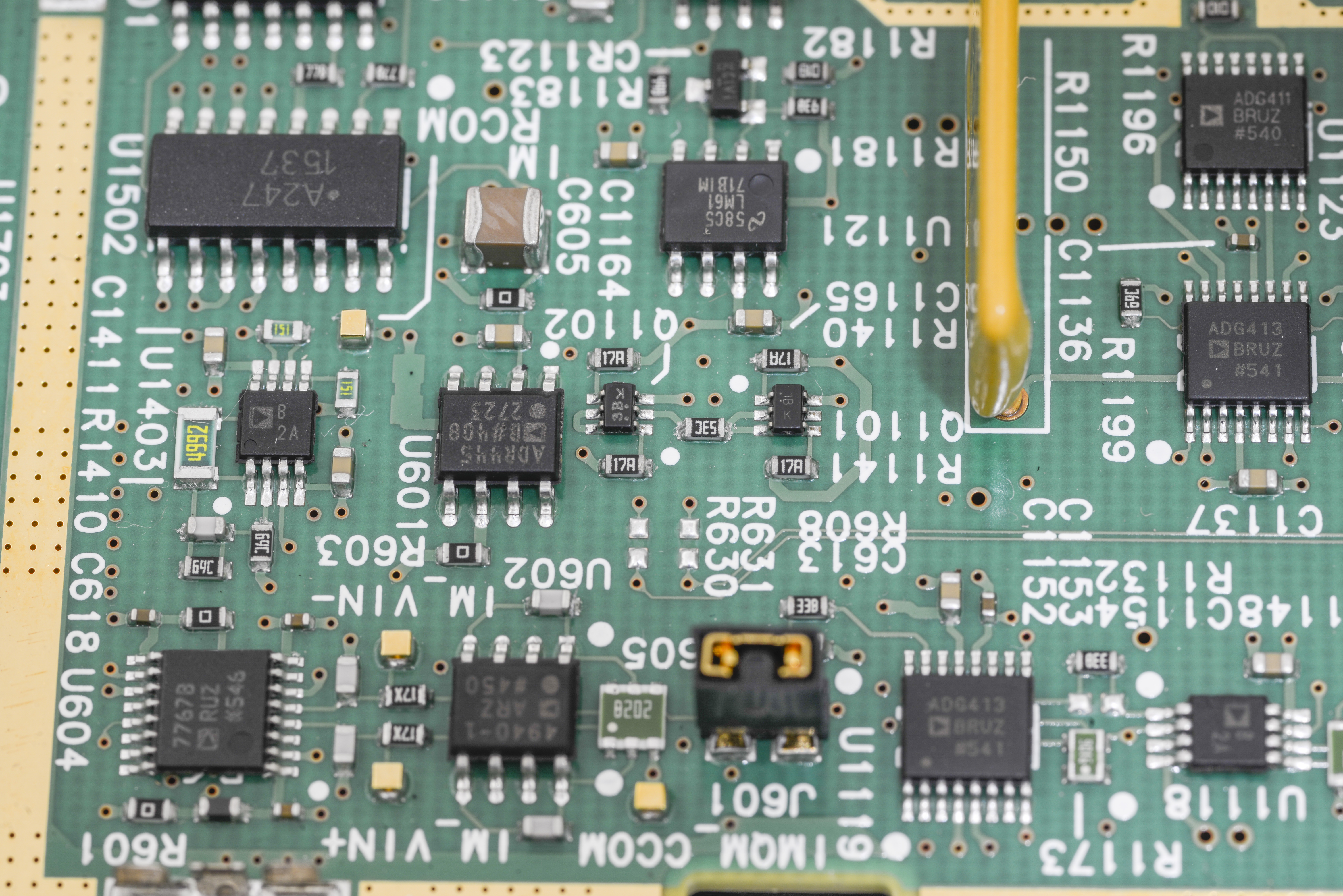
Image : test
Little TSSOP chip marked U604 in the bottom left corner of the photo is Analog Devices AD7767BRUZ. This is 24 bit high-performance SAR A/D converter, capable for speeds up to 128 kSPS. DC performance is not bad, sporting maximum ±7.6 ppm INL and Gain drift 0.4 ppm/°C. Key parameter of this ADC would be large dynamic range, about 110 dB, depends on conditions.
It is not too often that we see SAR ADC used as main detector in instrument designed to provide 6½ digits of resolution.
But it’s not a surprise, because of B2987A’s ability to digitize inputs with 20 µs intervals to internal memory. It can provide up to 12500 readings/s to the GPIB interface.

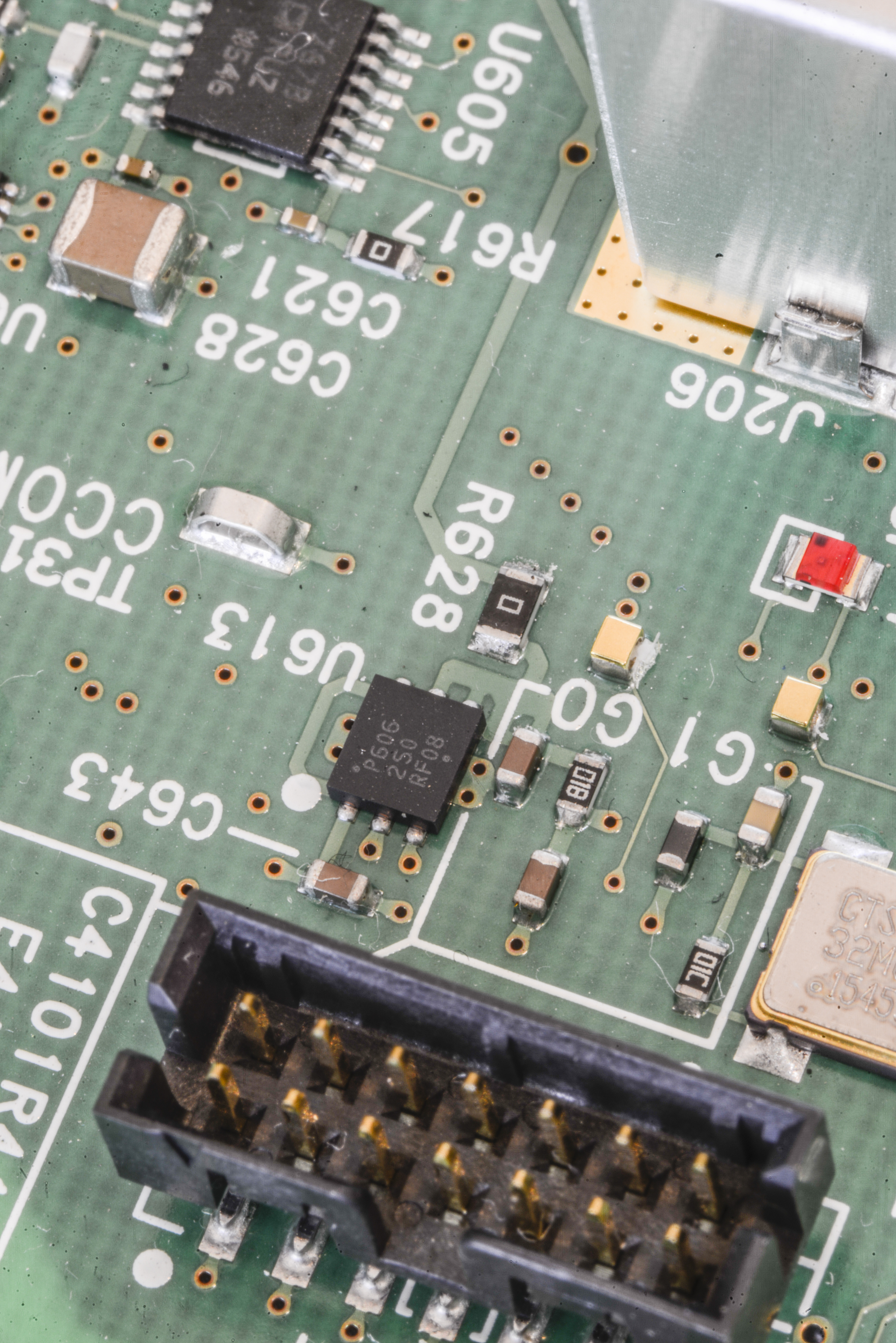
Image : test
Close-up macro photographs show surface condition of the PCBA. One can see some dust debri and particles present on the surface, so those guard rings and shield covers are definately put to test. Ideally instrument like this must be kept clean to maintain high sensitivity and good performance. However it is not easy to clean populated PCBA surface and would require lot of cleaning chemicals and baking to ensure high resistance isolation.
Other technique to mitigate PCB leakage is to use PTFE standoffs, however it’s only viable for thru-hole components and makes circuit board much larger physically (also larger area for guarding against leakage). This method was often used back in the days of thru-hole assembly decades ago, but as this special case demonstrate old tricks can be very useful even today.
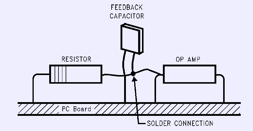
Image : Texas Instruments LMC662 Opamp datasheet shows air wiring method for sensitive signal
Older HP/Agilent/Keysight instruments are also known to implement manually-assembled air wiring design, for example in Agilent 41421B Source-Measure Unit module designed for Agilent 4142B semiconductor parametric analyzer.
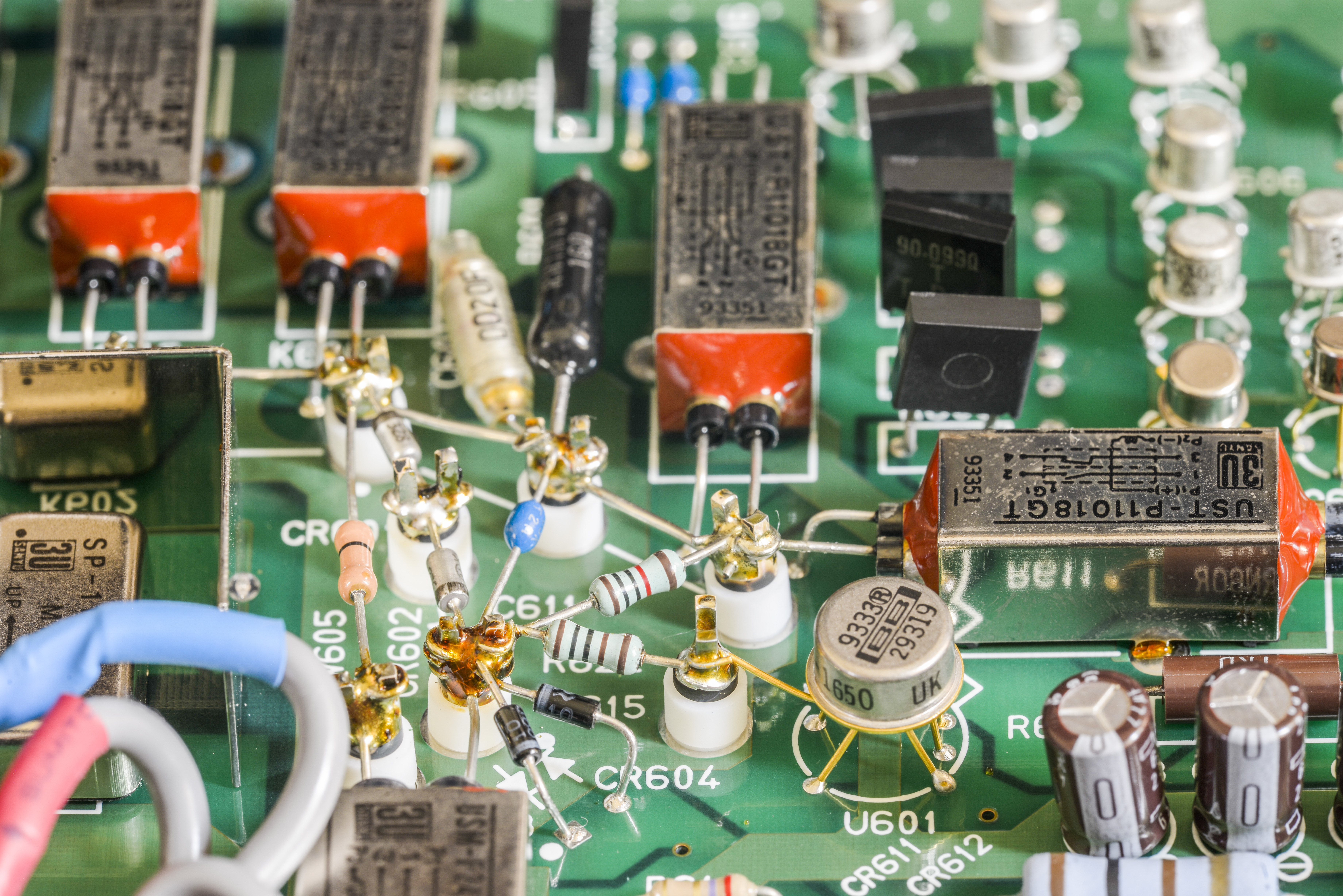
Image 5: PTFE-turret method of low-leakage circuit design, Agilent 41421B MPSMU
Photograph of exposed SMU front-end reveals isolated assembly with PTFE standoffs, pressed into the standard PCB board.

Image : test

Image : test
Guard shielding metal is all that exposed gold-plated area you see under the covered area. Surface leakage would be cought by exposed metal and prevent the sensitive signal loading and coupling. Guarding also reduce parasitic capacitance, because there is also no charge to accumulate between equal potentials.
Common and effective way to reduce the leakage current is to use the guarding technique. Enclosing the entire electrical signal path connected to the ammeter by the conductive material, but biased at the identical voltage level by additional low-impedance source, equal in potential to ammeter input terminal called guarding. Guarding also implemented in special cables between instrument input and device under test, by using triaxial low-noise cables, which have not one but two inner shields, separated by different dielectric layers. Inner shield in triaxial cable biased by guard voltage, removing leakage to center signal conductor, while outer shield is connected to common or ammeter Lo.
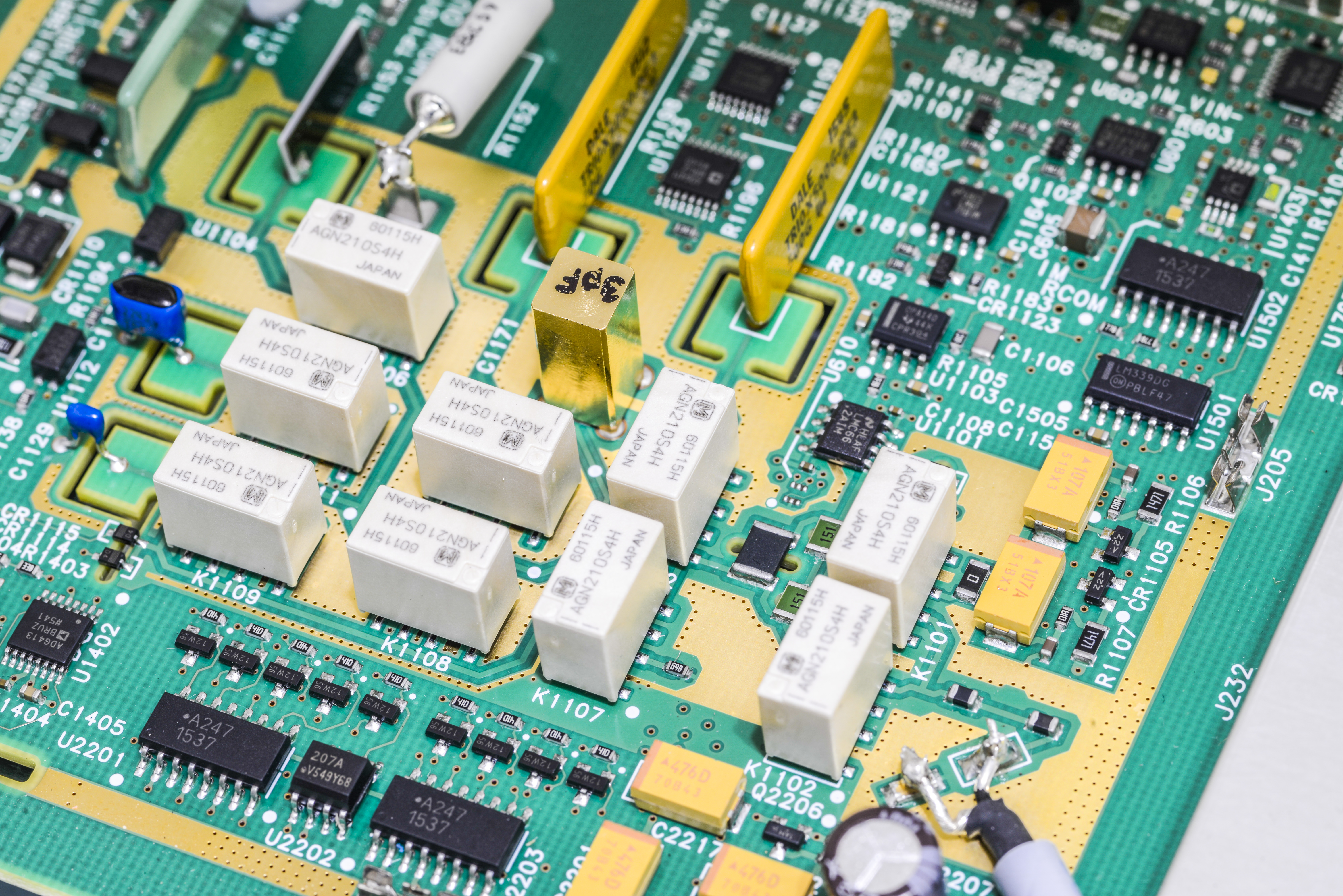
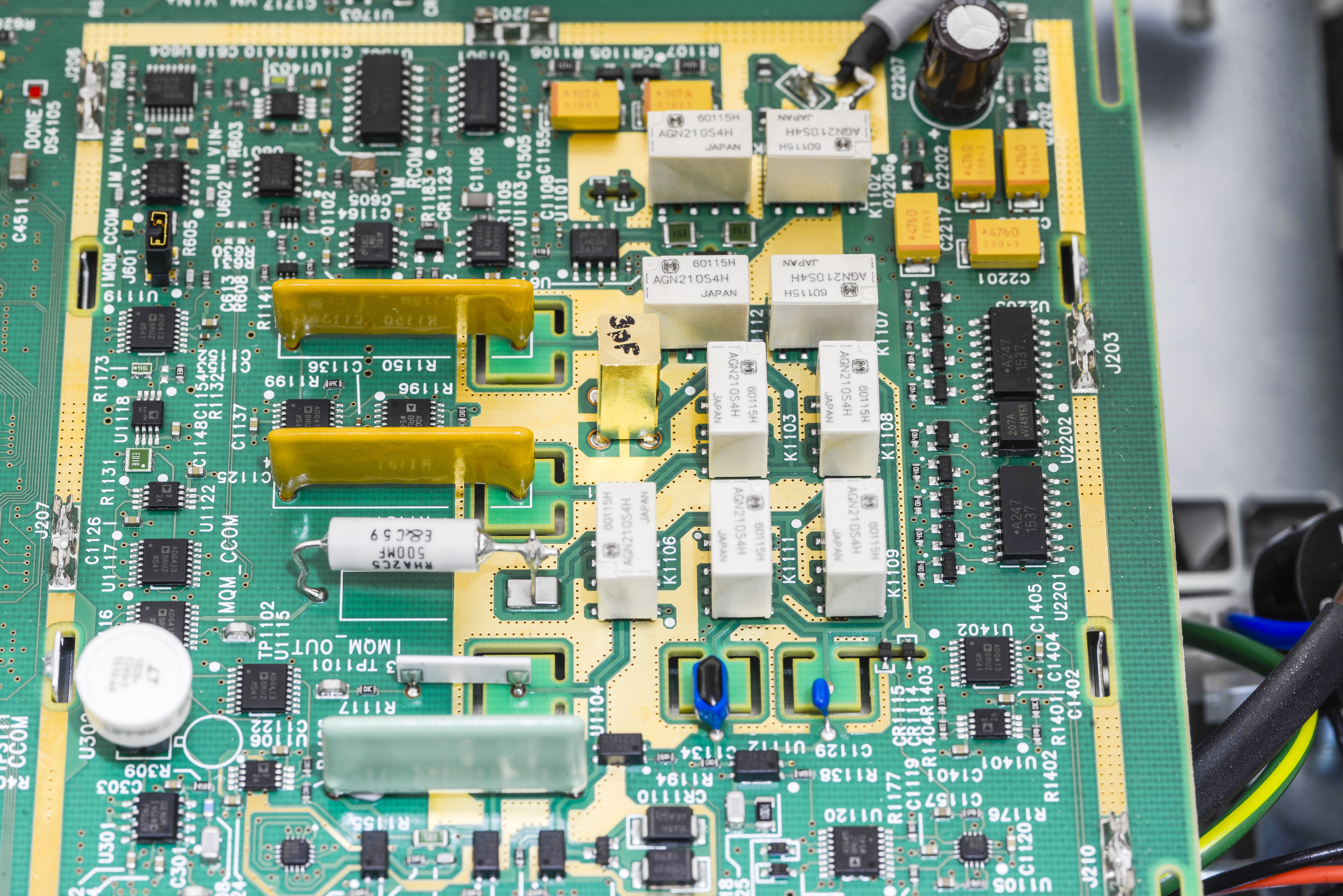
Image : test
Pretty looking hermetic gold-plated reference 3.3pF capacitor used in integrator. Together with feedback resistor this network set bandwidth limit of the current input front-end. 500 GΩ feedback resistor at most sensitive 2 picoamp range together with 3.3pF capacitor have bandwidth limited at 1.7 seconds (DC to 0.588 Hz). In typical configuration with oversampling meter produce useable data each 16 seconds. Next higher 20 picoamp range use 10 times smaller resistor that translate bandwidth into magnitude faster response (DC to 5.88 Hz). This idea follows for higher ranges, with fastest response of 100 µs on milliamp ranges.
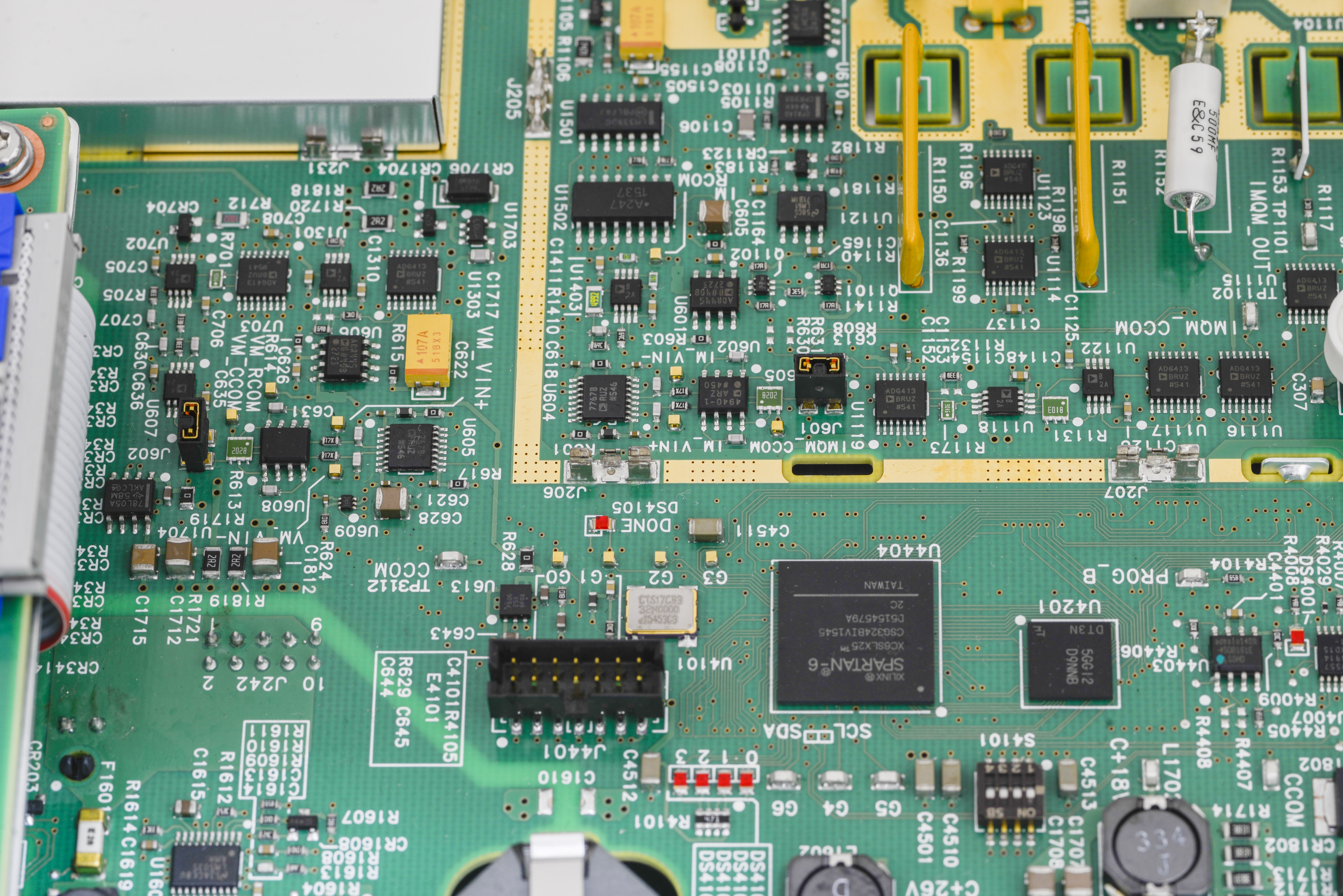
Image : test
This concept may sound easy, but actual hardware design and component selection for electrometer front-end requires very careful design. Working with femtoamp level signals from the input triax port requires full guarding and isolation from any signaling or power nodes. Any stray currents from the instrument’s circuitry, digital control signals or power regulators that may leak into the input node will cause errors the measurement. Running input signals across PCBA make it even more difficult as leakage in board material is not easy to characterize. Would not be surprising if Keysight carefully tested and selected special material for the outer dielectric layers of this analog board to keep PCB leakage in check.
The instrument’s exposure to changing environment in both temperature, humidity and pressure affect performance as well. Humidity and temperature both have major impact on dielectric surface resistance. To provide better confidence in results it is useful to track and sync environment monitoring data together with measured currents/voltages. That is why Keysight B2980A series, well as Keithley 6517 series have thermocouple and humidity sensor inputs, so related data can be captured by same instrument in the lab.
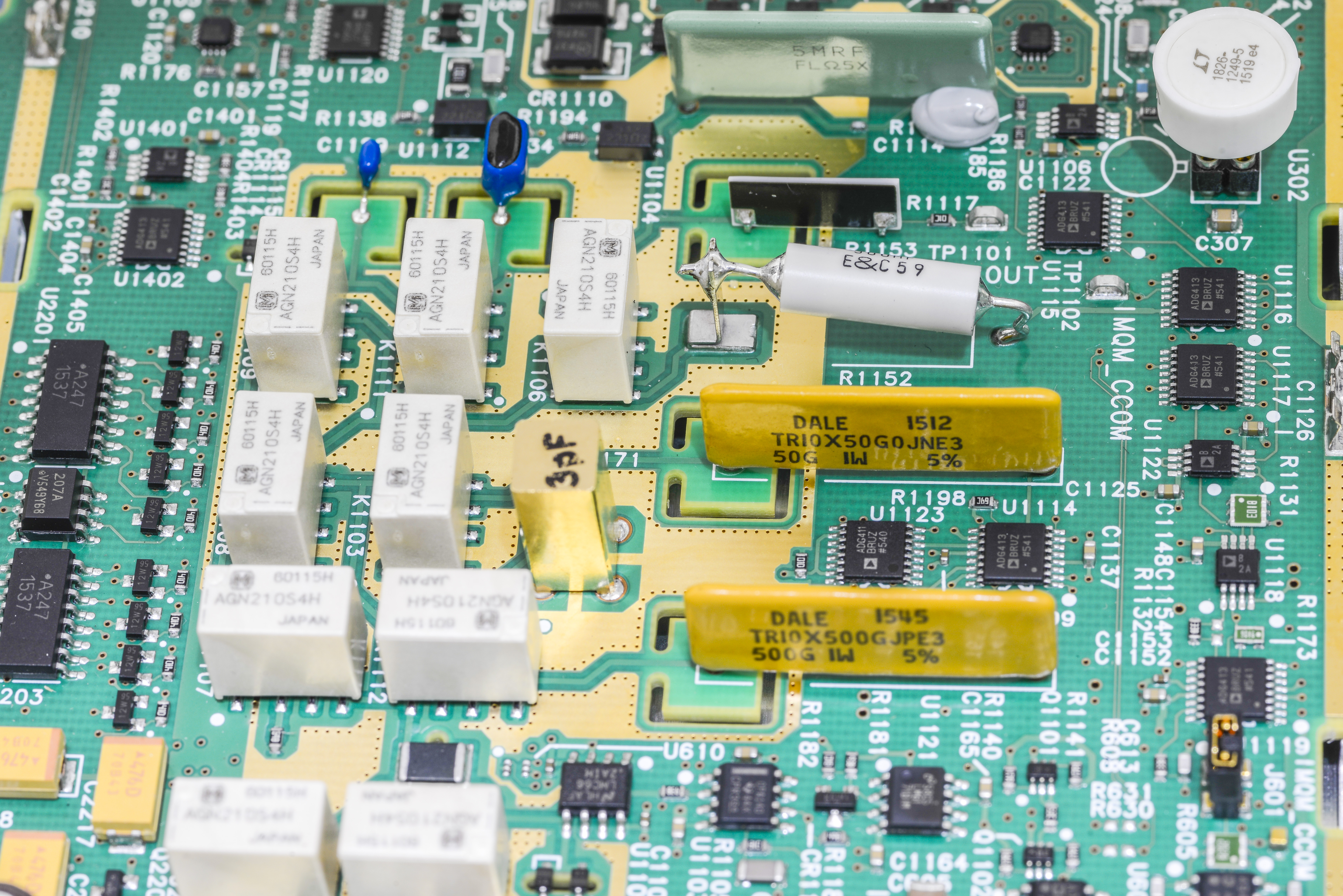
Image : test
Vishay TR10X high-voltage thick-film resistors are used in input opamp feedback path, selected according to used current range. Highest value is 500 GΩ with 5% tolerance, rated working voltage 10kV. Temperature coefficient of these high-value resistors rarely good, confirmed by specification 500 ppm/°C. Usually that is not a problem as temperature correction can be applied or calibrated out, however voltage coefficient (change of resistance under applied voltage) is more important specifications. And sure enough, these TR10X resistors are specified for better than 1 ppm/V VCR.
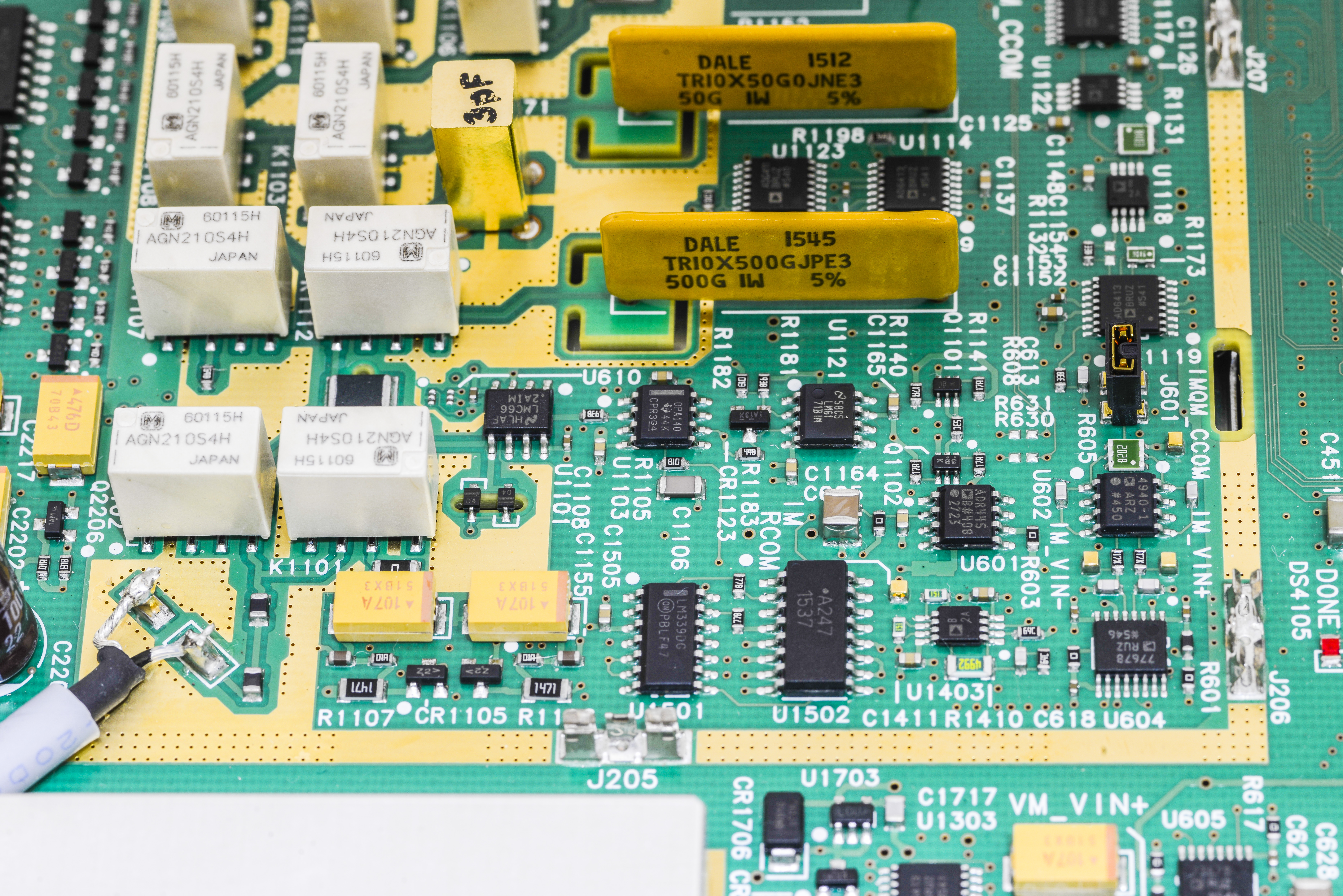
Image : test
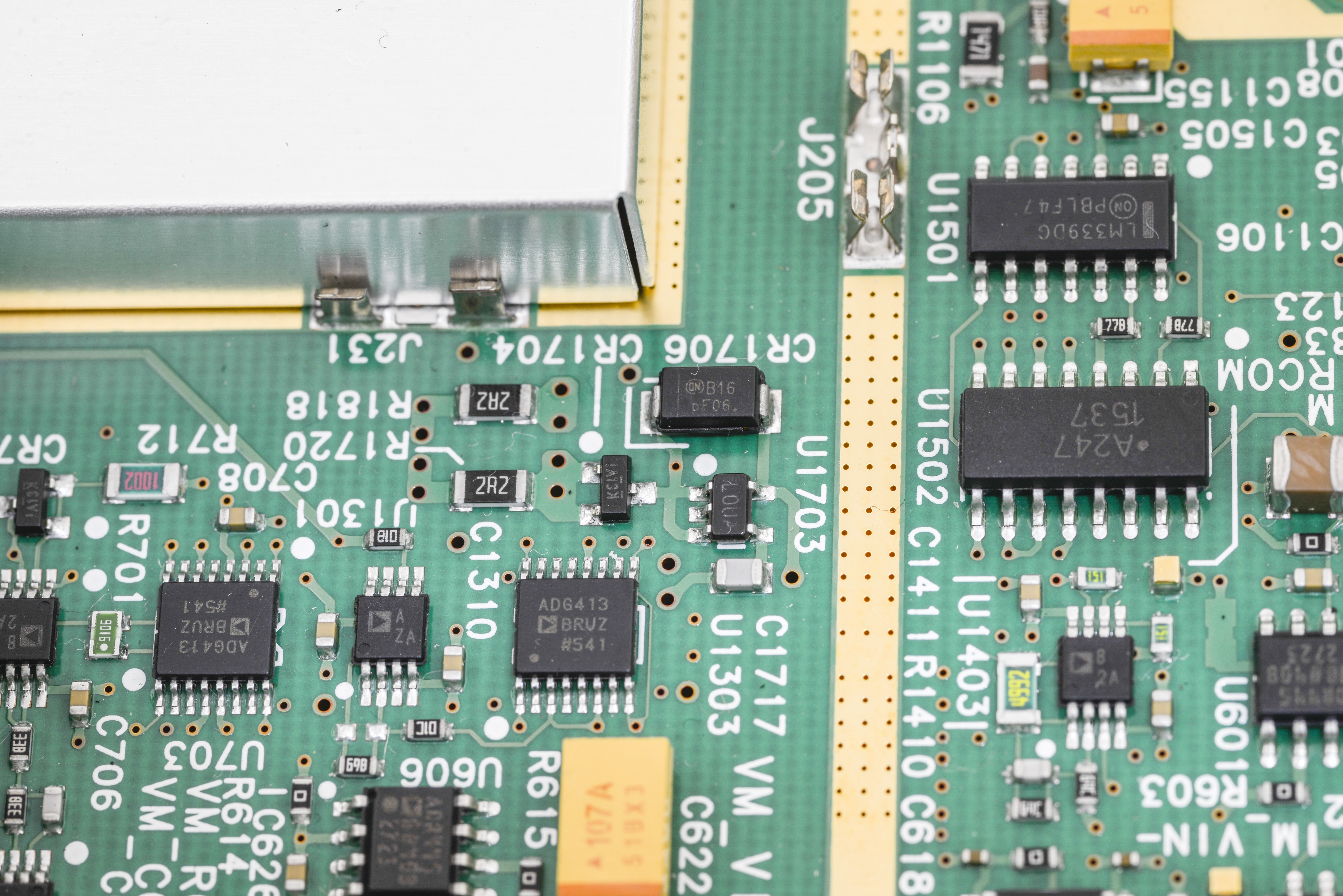

Image : test
Voltage meter input have separate guarded can on top PCBA surface. It is obvious because voltage and current inputs are separate in B2987A and can be driven to different guard levels, according to measured signal potentials.

Image : Voltage input front-end with guard shield removed
Voltage input front end have Texas Instruments LMC662 dual opamp with ultra-low input bias and offset current (maximum 2 pA, typical 2 fA!)
three SMD of 10Kohm and MKP3VI20 TVS
relays are M TQ2SA-5V SMT
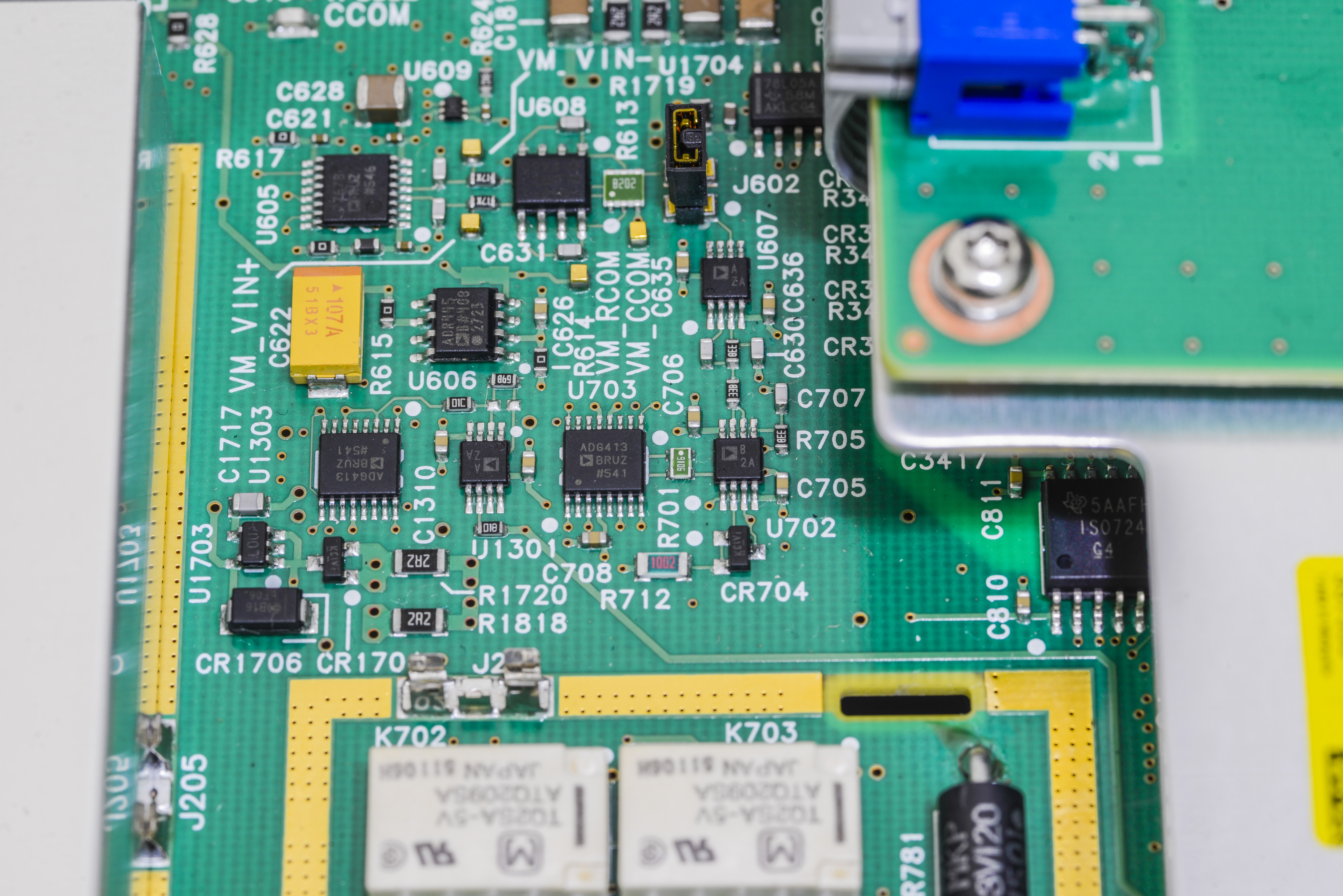
Image : test
Core of the voltage measurement function in B2987A is Analog Devices AD7767BRUZ 24-bit 32/64/128 kSPS SAR ADC. It has ±7.6 ppm maximum INL specification and able to provide over 100 dB of dynamic range, when used with 5V voltage reference. And that is exactly what is present onboard next to ADC chip, in shape of Analog Devices XFET® ADR445. This reference designed to provide 5.000 VDC with initial accuracy ±2 mV and temperature stability 3 ppm/°C. It’s low noise reference, with 2.25 µVpk-pk typical over 0.1 – 10 Hz bandwidth. Pair of ADG413BRUZ used to for inputs multiplexing and range switching. Voltage measurement function in electrometer have just two ranges, ±2 V and ± 20 V. Based on brief circuit analysis base range is 2 V, while higher range use x10 attenuation by front-end before ADC.
There are also three Analog Devices OP1177ARMZ amplifiers
Datasheets for all these components available for detailed study:
AD7767 24-bit SAR ADC Data Sheet, Rev.C
Analog Devices XFET® ADR440-ADR445 series voltage reference datasheet
ADG411/412/413 series Precision Quad SPST Switches datasheet
OP1177/2177/4177 Precision Low Noise, Low IB Opamp Datasheet
78L05 regulator in SO8
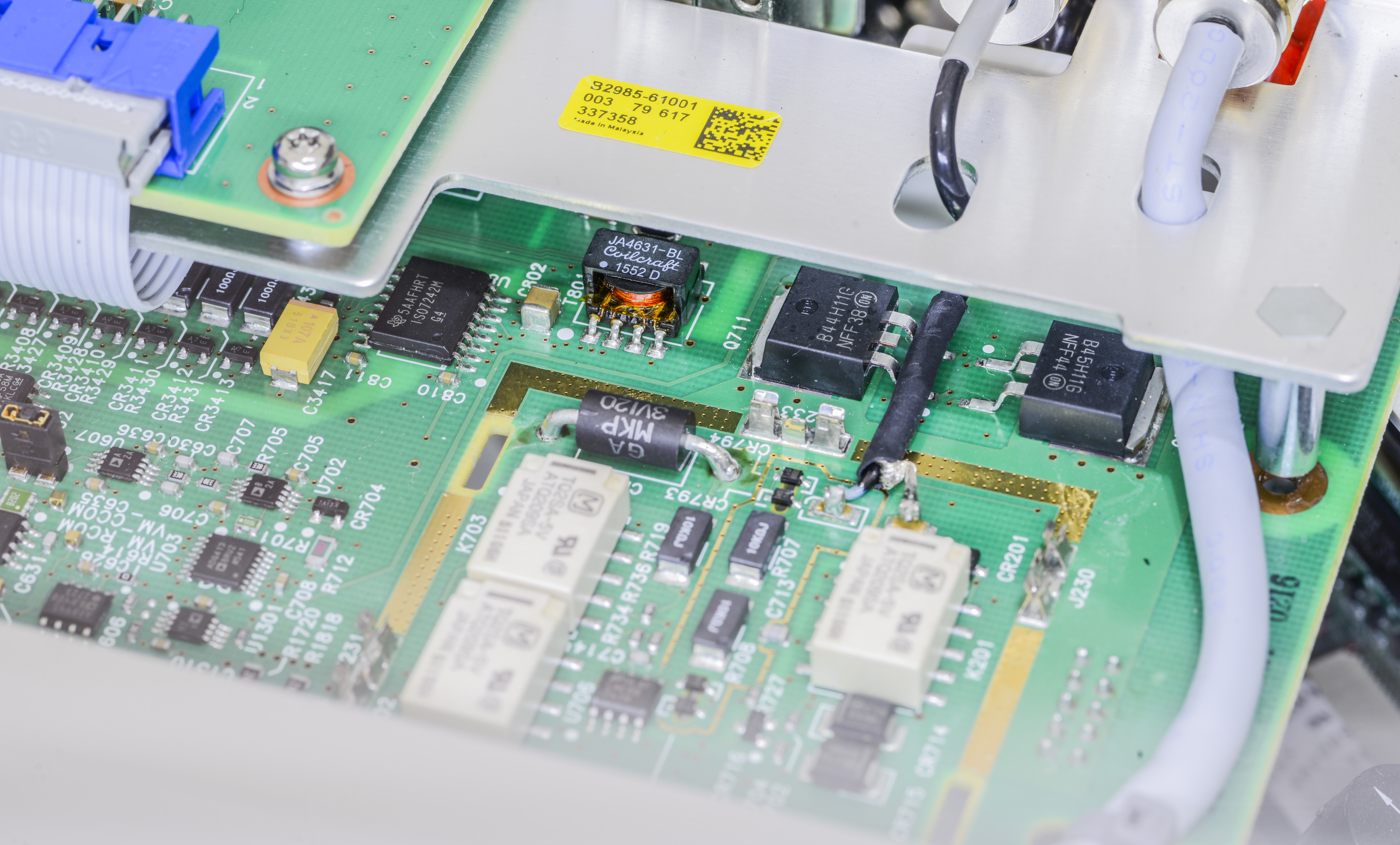
Image : test


Image : test
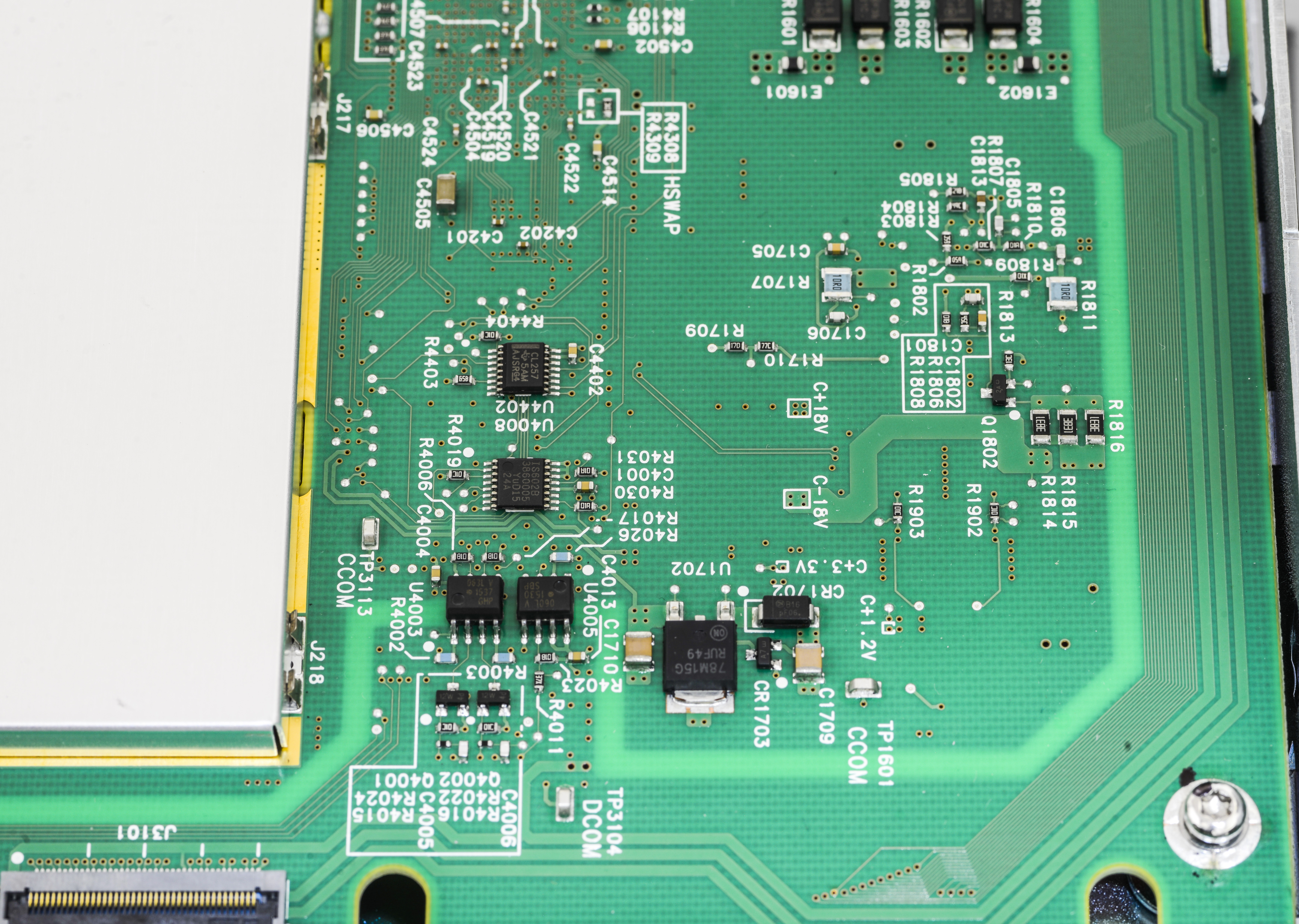
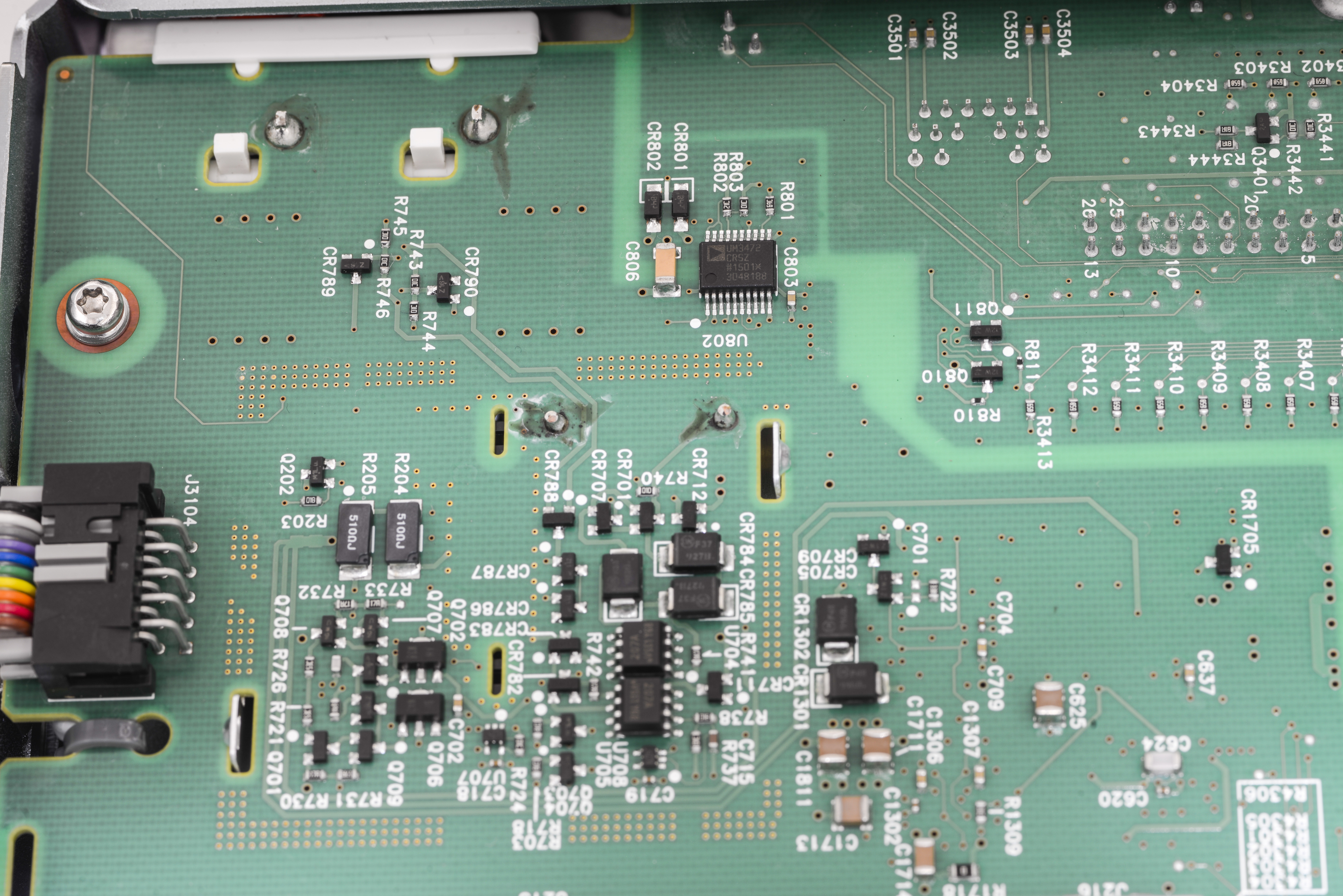
Image : test
There you have it, Keysight B2987A Electrometer/High-resistance meter in it’s beautiful construction and design. Now time to reassmemble meter together and perform some experiments.
Battery installation and initial checks
Before we dive into performance and experiments, let’s install some compatible battery. This enable field operation of the unit, and hopefully will help us to evaluate noise performance with and without mains power, if there is any visible difference.
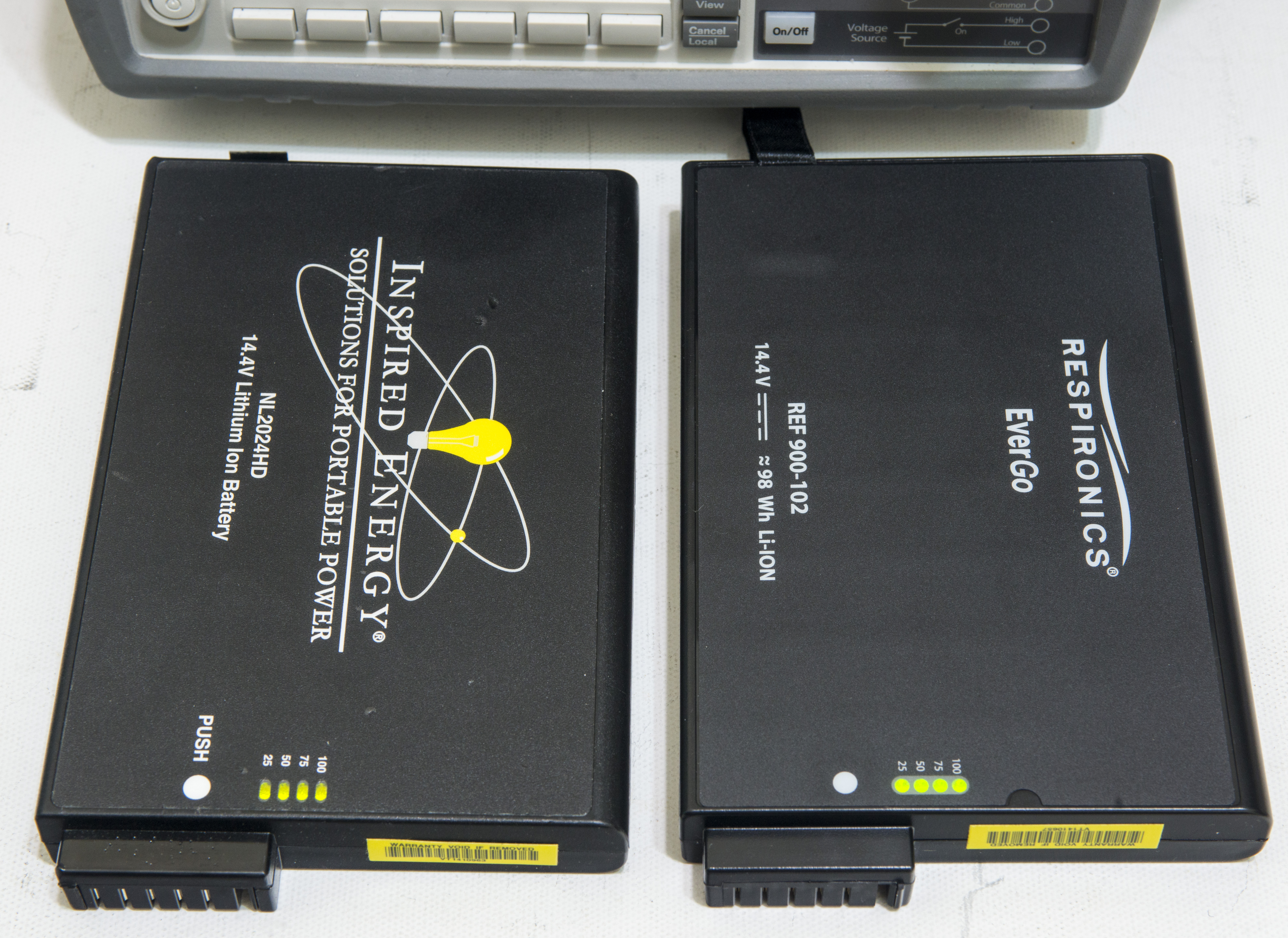
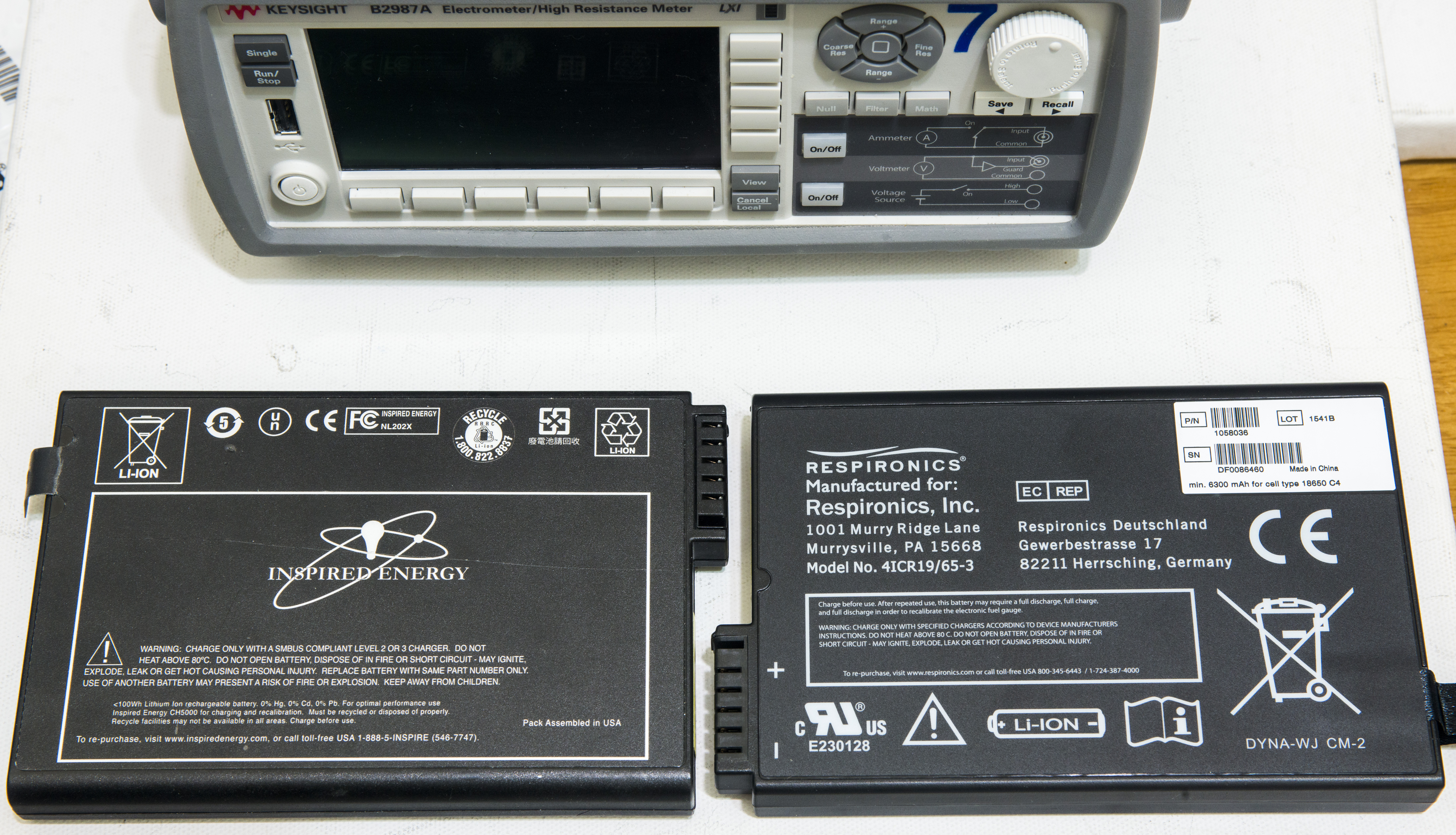
Image : test
We got two battery packs, one from Inspired Energy, model NL2024HD and second is RESPIRONICS REF900-102. Both packs have same configuration, form-factor and can be installed in B2987A.

Image : test
After installation unit can charge battery normally and also report the battery charge cycle correctly:
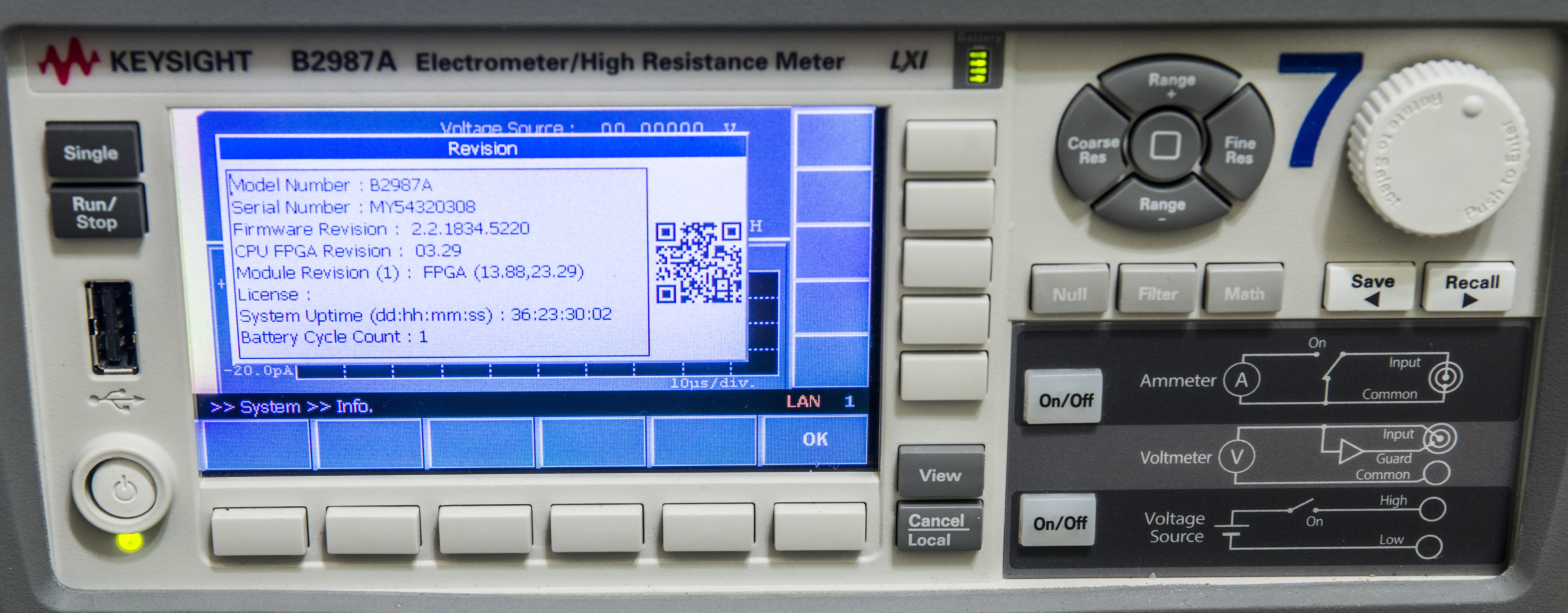
Image : test
Firmware and software

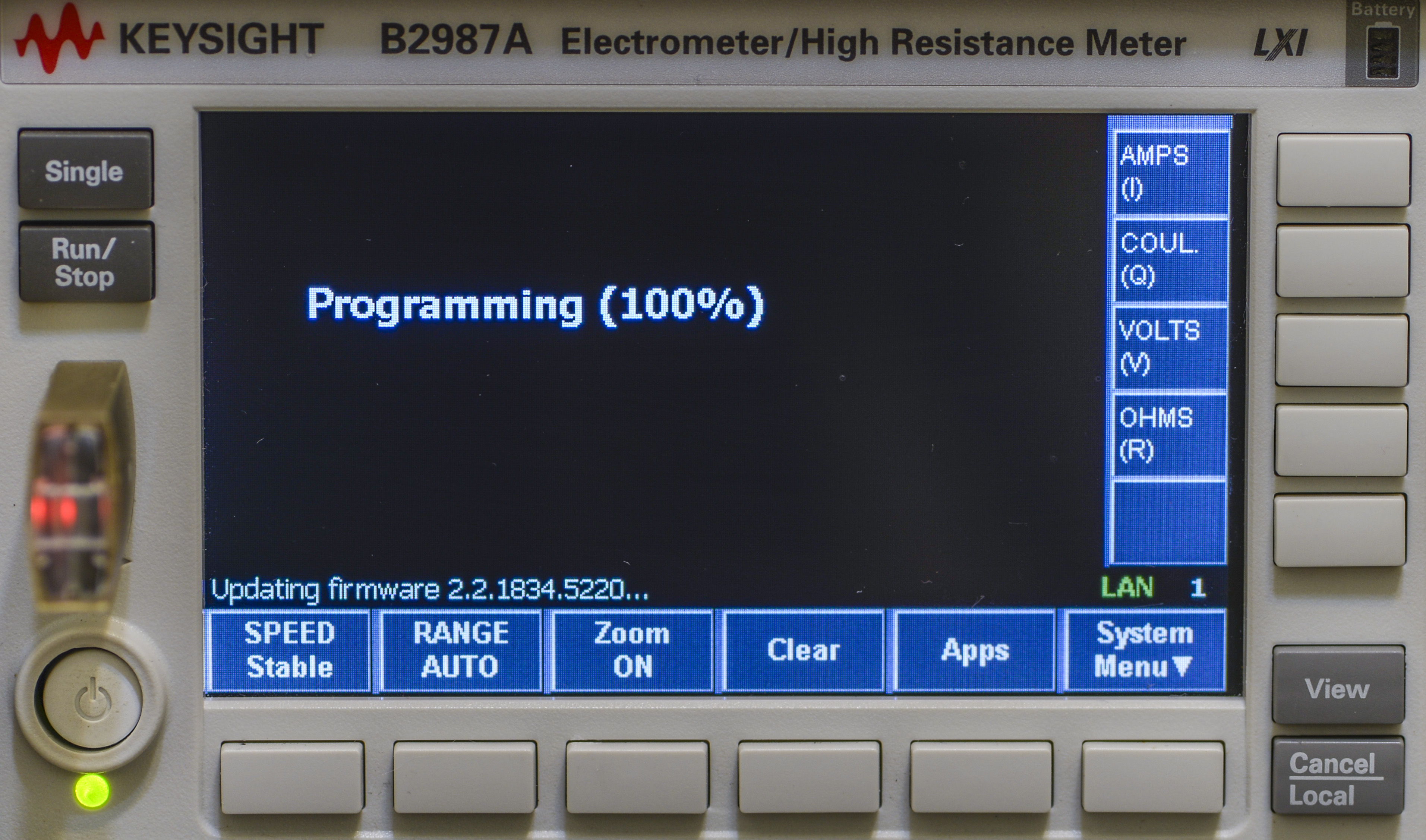
Image : test
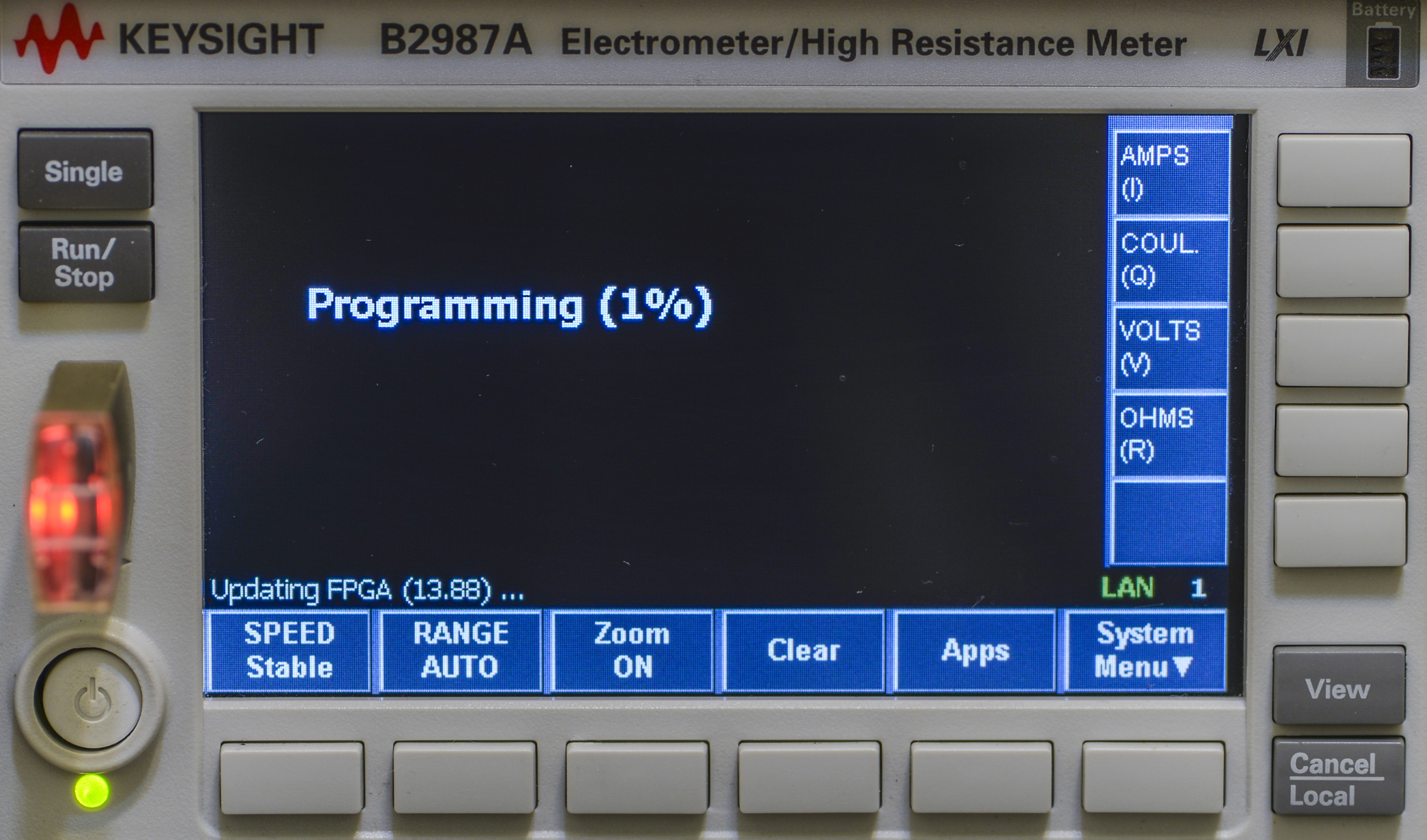
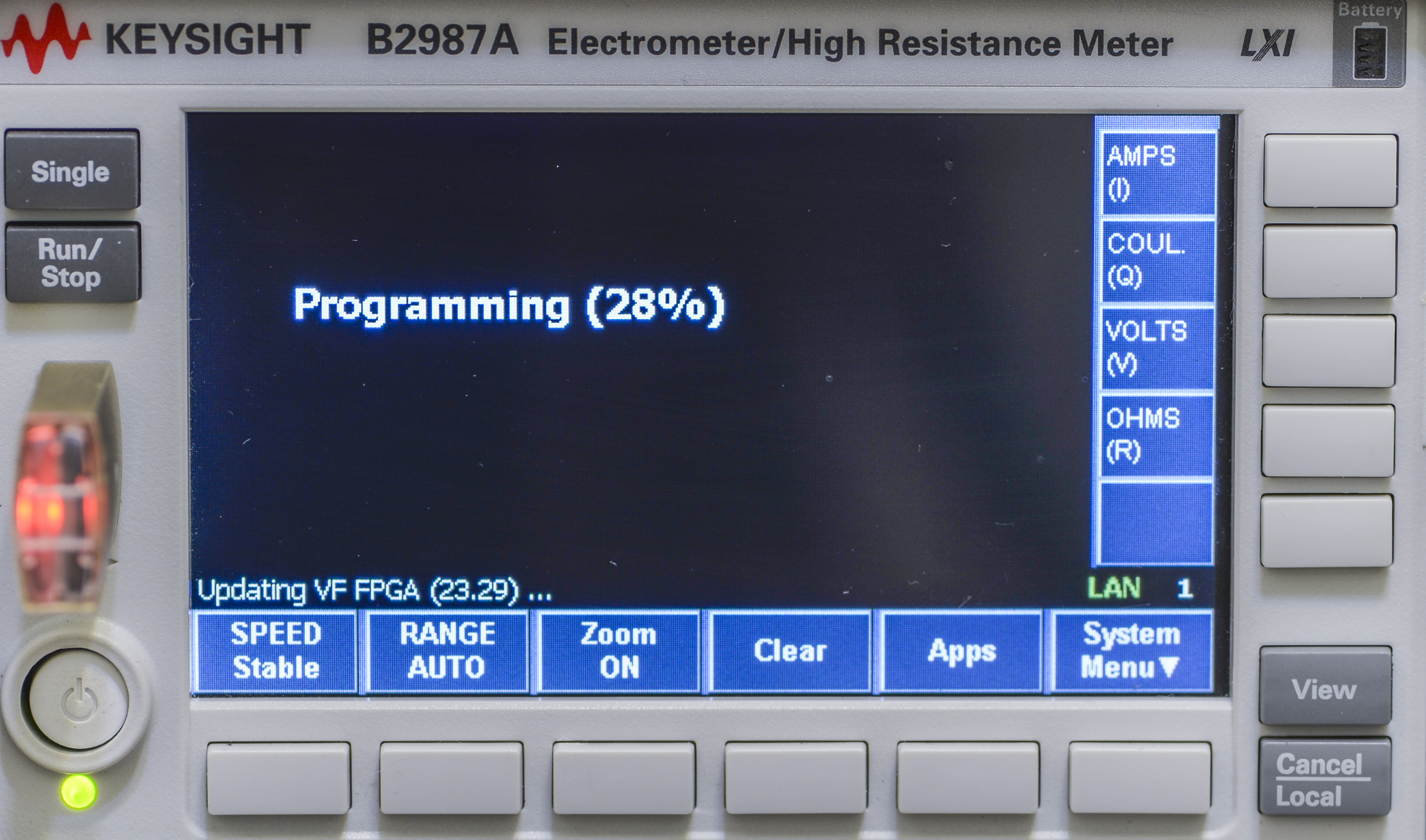
Image : test

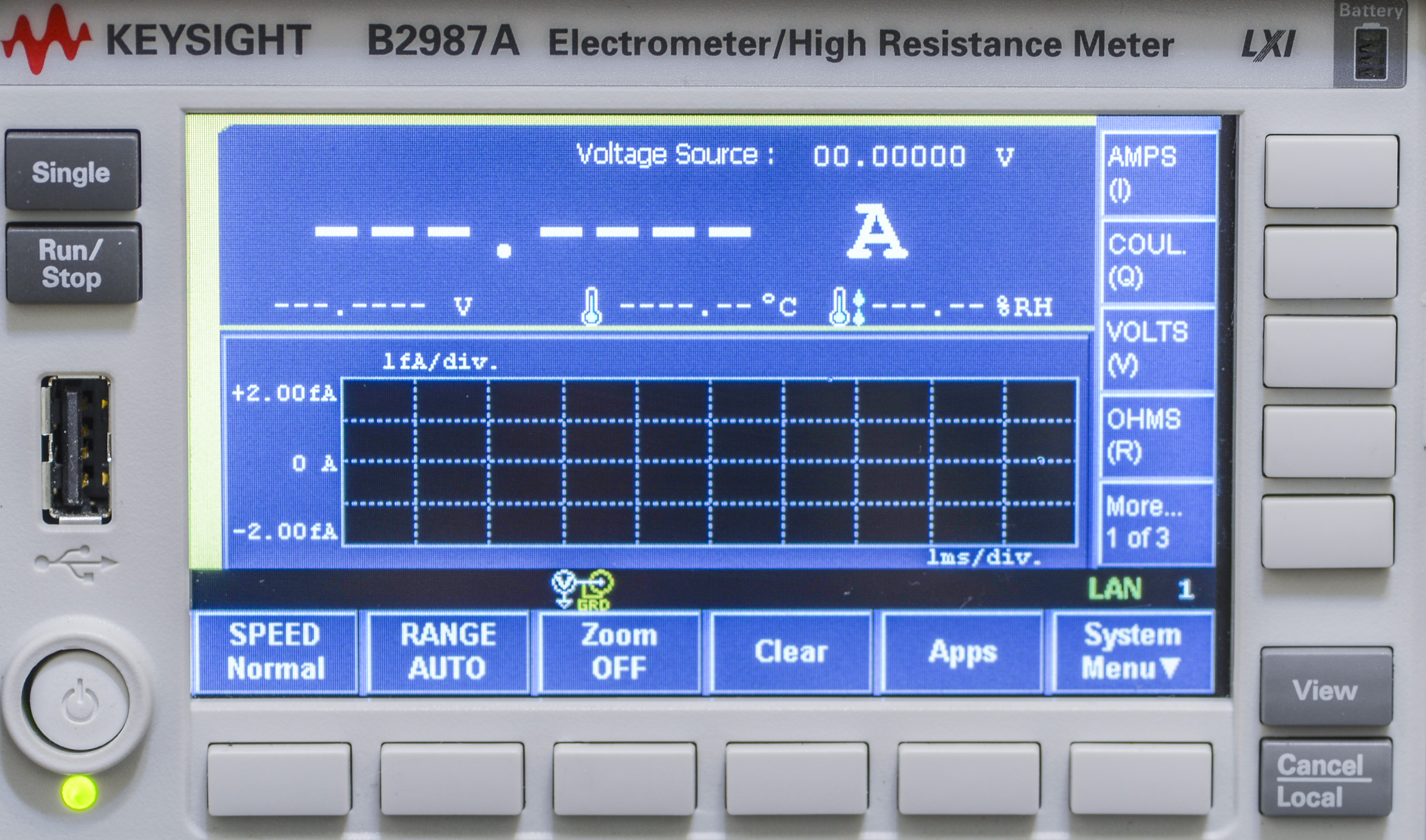
Image : test
Firmware revision as received : 2.2.1745.7190
CPU FPGA version: 03.29
Module Revision : FPGA, (13.88, 23.29)
License: None
System uptime: 3 day 3 hour 39 min 15 sec
Battery Cycle count: 0 (no battery installed)
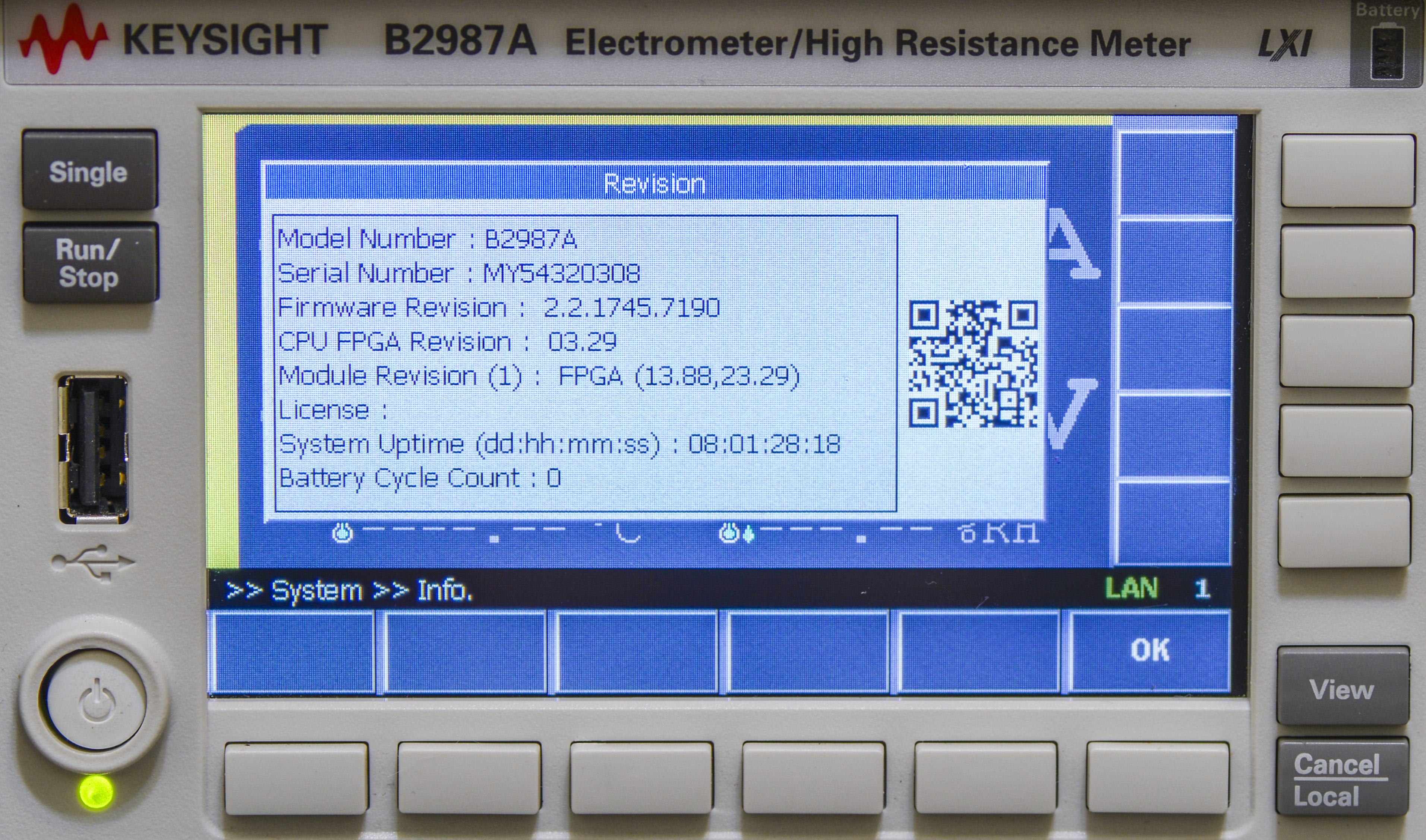

Image : test
Firmware blobs are unified and available for all B2980A series instruments for user upgrade.
| Firmware revision | Released binary |
|---|---|
| B2980A series firmware 2.3.2011.5670 (latest) | ZIP-archive |
| B2980A series firmware 2.3.1924.2760 | ZIP-archive |
| B2980A series firmware 2.3.1916.4990 | ZIP-archive |
| B2980A series firmware 2.3.1902.5305 | ZIP-archive |
| B2980A series firmware 2.2.1834.5220 | ZIP-archive |
| B2980A series firmware 2.2.1745.7190 | ZIP-archive |
| B2980A series firmware 2.1.1645.5880 | ZIP-archive |
| B2980A series firmware 2.0.1608.8800 | ZIP-archive |
| B2980A series firmware 1.1.1527.1533 | ZIP-archive |
| B2980A series firmware 1.1.1508.3400 | ZIP-archive |
| B2980A series firmware 1.0.1430.6131 | ZIP-archive |
Release notes with changes and fixes
Keysight also provides software to remotely control and interface with the instrument:
| Description | Released binary |
|---|---|
| QuickIV ver.4.1.1821.3680 software suite | Binary setup file |
Web-interface
Nearly useless, thanks to obsoleted Java :). Keysight have even dedicated page from 2015 year that acknowledge this issue, showing hops required for Java stuff.
Initial check results
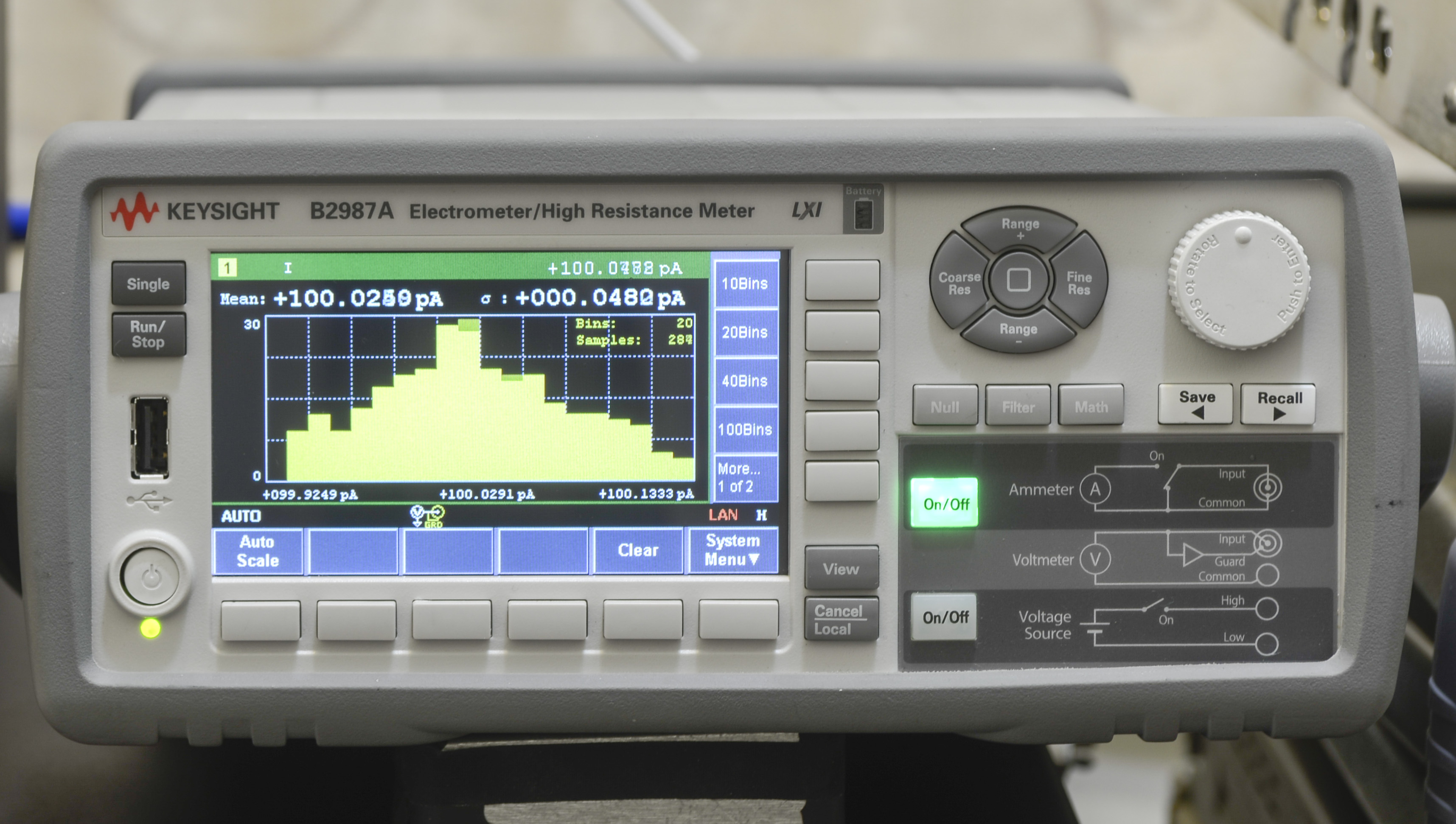
Image : 100 pA benchmark test
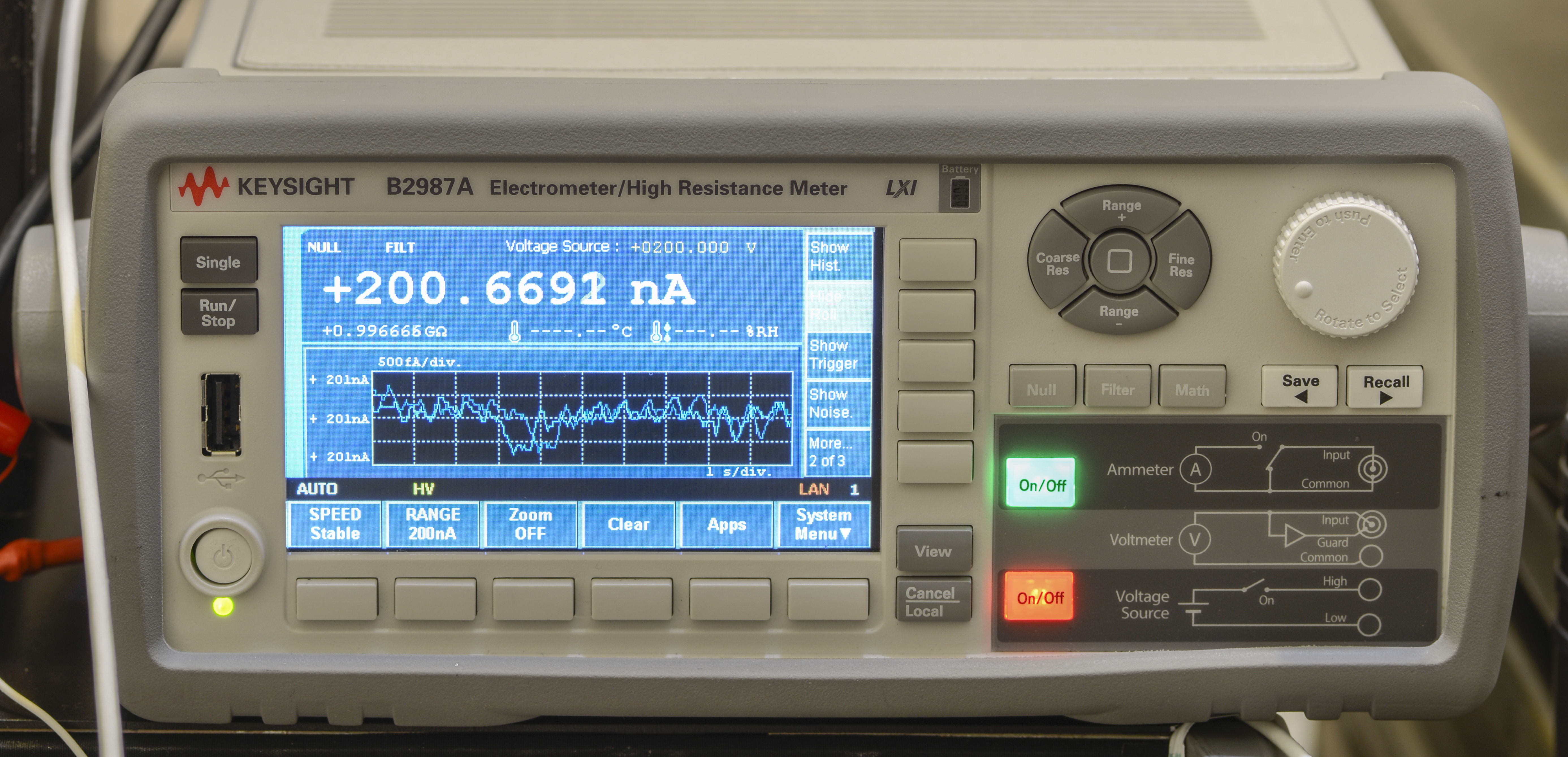
Image : 200 nA benchmark test
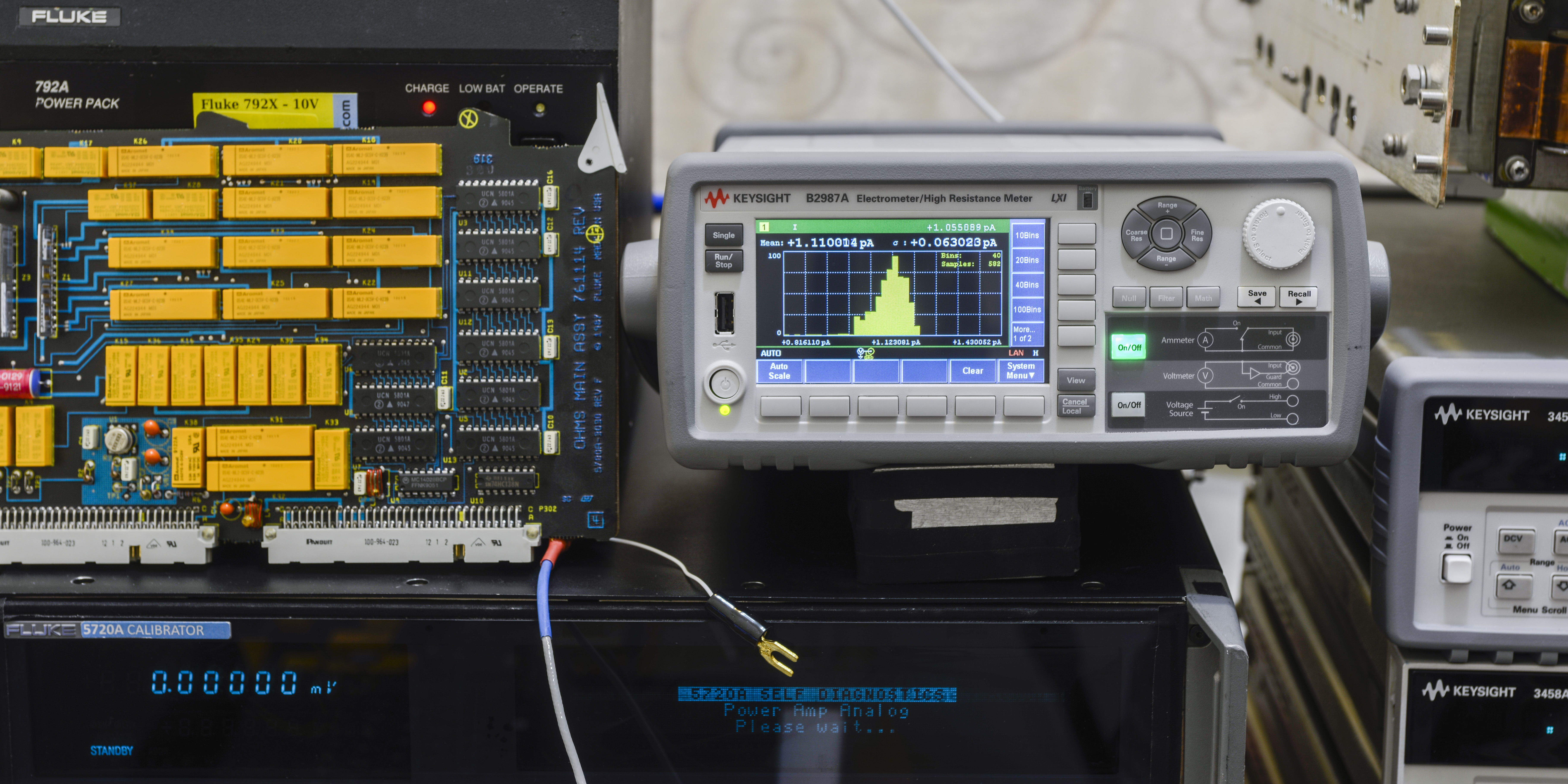
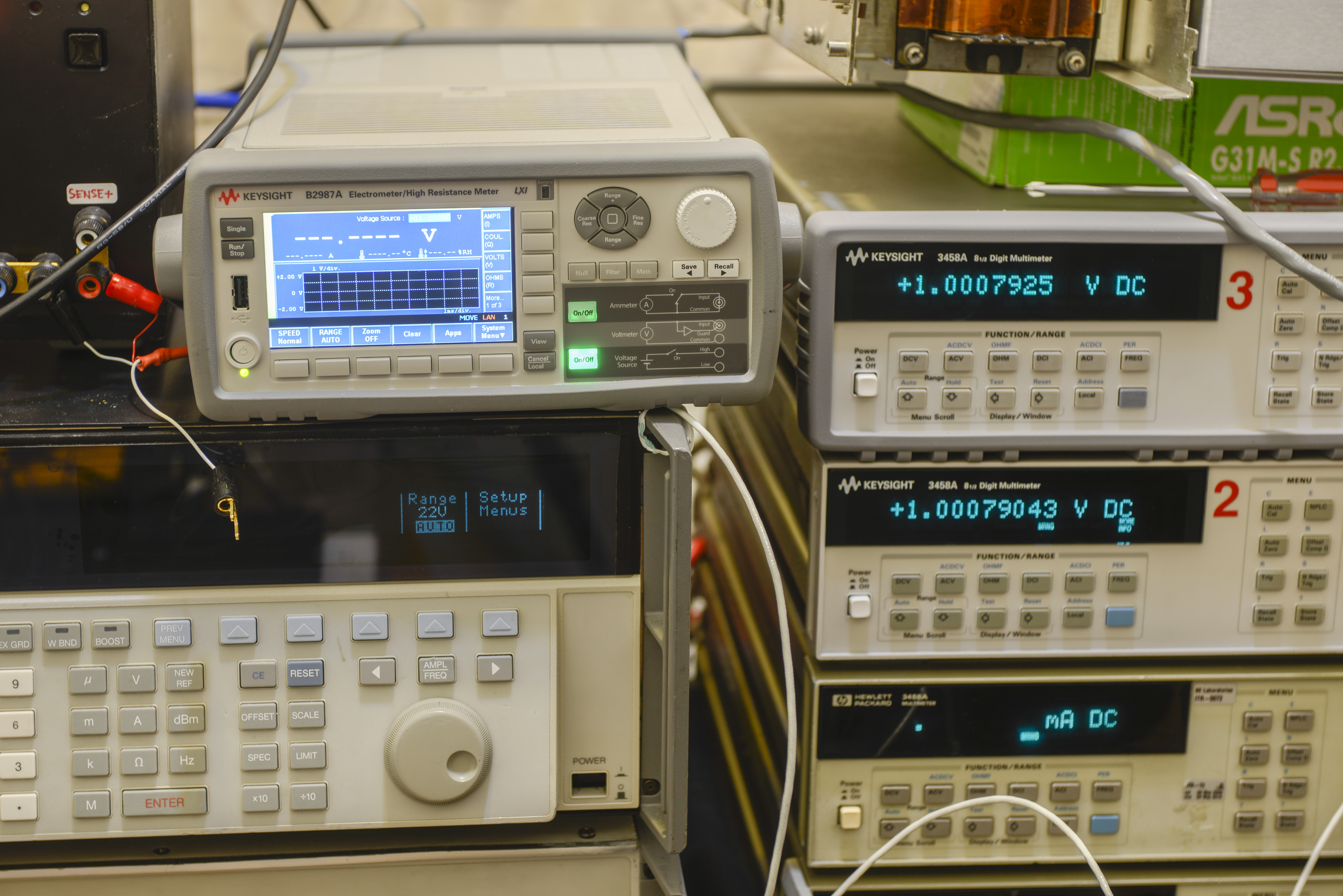
Image : 1 pA and 1 VDC tests
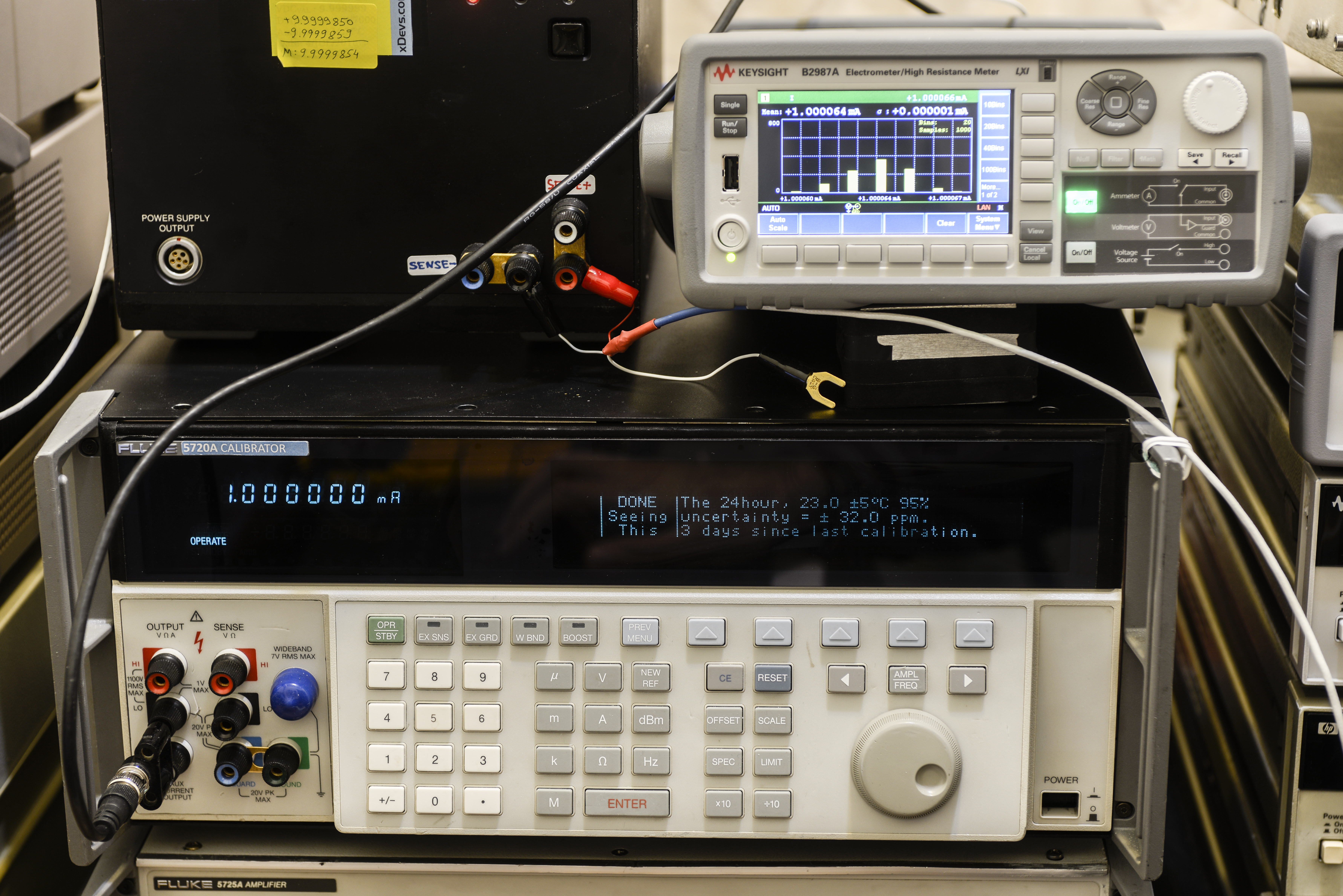
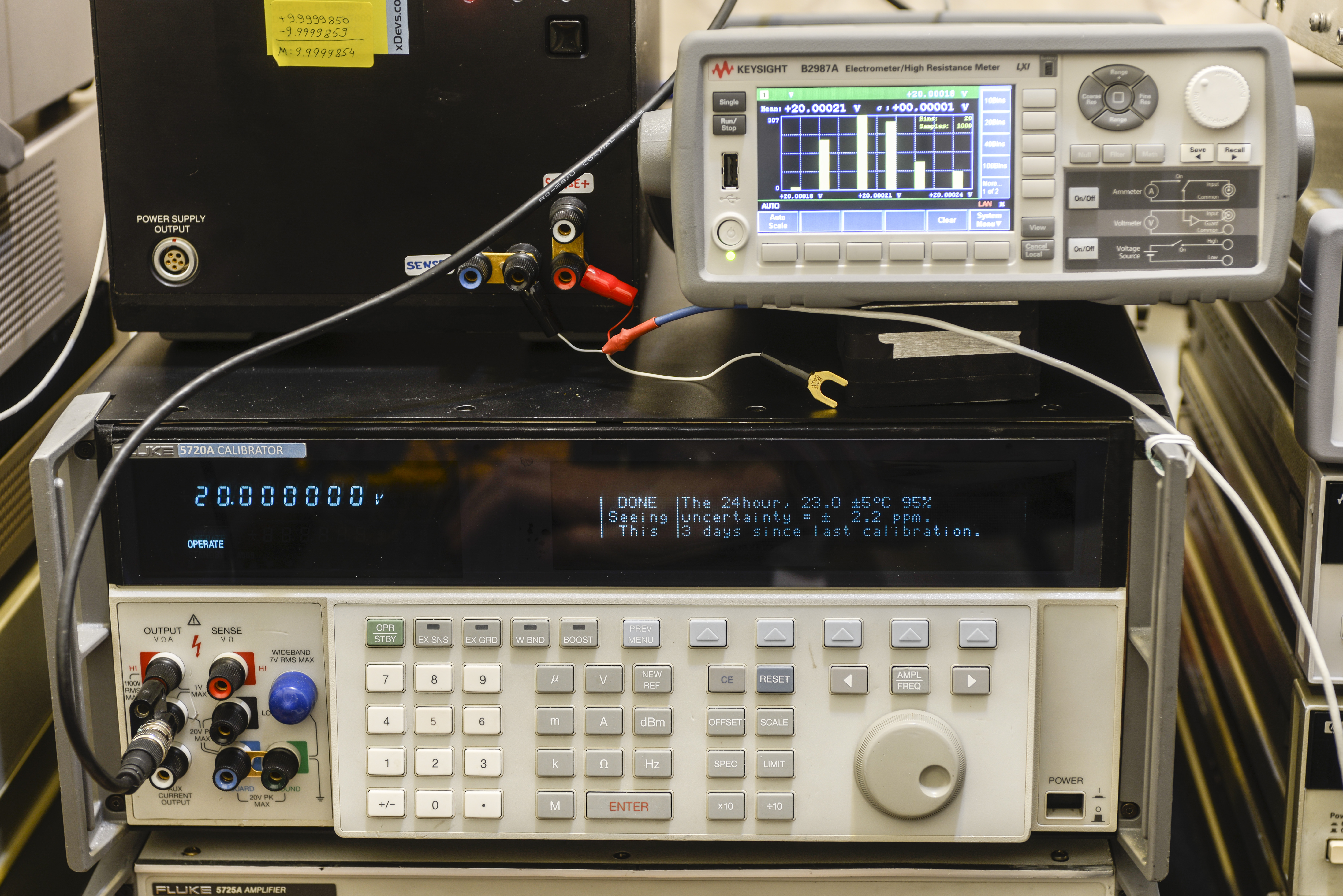
Image : 1mA and 20 VDC tests
| B2987A function, range | Measurement result | Source value | Specification | Settings |
|---|---|---|---|---|
| 10 mA | 10.00050 mA, sdev: 00.000001 mA | 10mA, 5720A/HLK | ||
| 1 mA | 1.000063 mA, sdev: 0.000001 mA | 1 mA, 5720A/HLK | ||
| 100 µA | 100.0083 µA, sdev:0.0001 µA | 100 µA, 5720A/HLK | ||
| 10 µA | 10.00093 µA, sdev:0.00004 µA | 10 µA, 5720A/HLK | ||
| 10 µA | 10.00047 µA, sdev:0.00004 µA | 10 µA, Keithley 6221 | ||
| 1 µA | 0.999997 µA, sdev:0.000154 µA | 1 µA, 5720A/HLK | Aux output, usµAl BNC to BNC-triax adapter on EM | |
| 1 µA | 1.000026 µA, sdev:0.000002 µA | 1 µA, Keithley 6221 | ||
| 100 nA | 100.0294 nA, sdev:0.00004 nA | 100 nA, Keithley 6221 | ||
| 10 nA | 10.00339 nA, sdev:0.00006 nA | 10 nA, Keithley 6221 | ||
| 1 nA | 1.000087 nA | 1 nA, Keithley 6221 | GµArd on, NPLC100 | |
| 100 pA | 100.0180 pA | 0.1000 nA, Keithley 6221 | ||
| 10 pA | 9.9908 pA, sdev:0.051 pA | 0.0100 nA, Keithley 6221 | ||
| 1 pA | 1.12308 pA, sdev:0.063 pA | 0.0010 nA, Keithley 6221 | ||
| -0.1 V | -0.099999, sdev:1 uV | 5720A/HLK | BNC to BNC-triax to Vin input EM | |
| 0.1 V | 0.100008, sdev:1 uV | 5720A/HLK | BNC to BNC-triax to Vin input EM | |
| -1 V | -1, sdev: 1uV | 5720A/HLK | BNC to BNC-triax to Vin input EM | |
| 1 V | 1.000010 V, sdev: 1uV | 5720A/HLK | BNC to BNC-triax to Vin input EM | |
| -10 V | -10.00007 V, sdev: 10uV | 5720A/HLK | BNC to BNC-triax to Vin input EM | |
| 10 V | 10.00013 V, sdev: 10uV | 5720A/HLK | BNC to BNC-triax to Vin input EM | |
| -20 V | -20.00013 V, sdev: 10uV | 5720A/HLK | BNC to BNC-triax to Vin input EM | |
| 20 V | +20.00023 V, sdev: 10uV | 5720A/HLK | BNC to BNC-triax to Vin input EM | |
| Vsource 0V | 3458A : 1.009 mV | Keysight 3458A/X02 REF | Output connected to 3458A+3458B | |
| Vsource 1V | 3458A : 1.000796 V | Keysight 3458A/X02 REF | Output connected to 3458A+3458B | |
| Vsource -1V | 3458A : -0.999262 V | Keysight 3458A/X02 REF | Output connected to 3458A+3458B | |
| Vsource 10V | 3458A : 10.000800 V | Keysight 3458A/X02 REF | Output connected to 3458A+3458B | |
| Vsource -10V | 3458A : -9.999027 V | Keysight 3458A/X02 REF | Output connected to 3458A+3458B | |
| Vsource 100V | 3458A : 100.0133 V | Keysight 3458A/X02 REF | Output connected to 3458A+3458B | |
| Vsource -100V | 3458A : -100.0130 V | Keysight 3458A/X02 REF | Output connected to 3458A+3458B | |
| Vsource 100V | 3458A : 999.9312 V | Keysight 3458A/X02 REF | Output connected to 3458A+3458B | |
| Vsource -1000V | 3458A : -999.9321 V | Keysight 3458A/X02 REF | Output connected to 3458A+3458B |
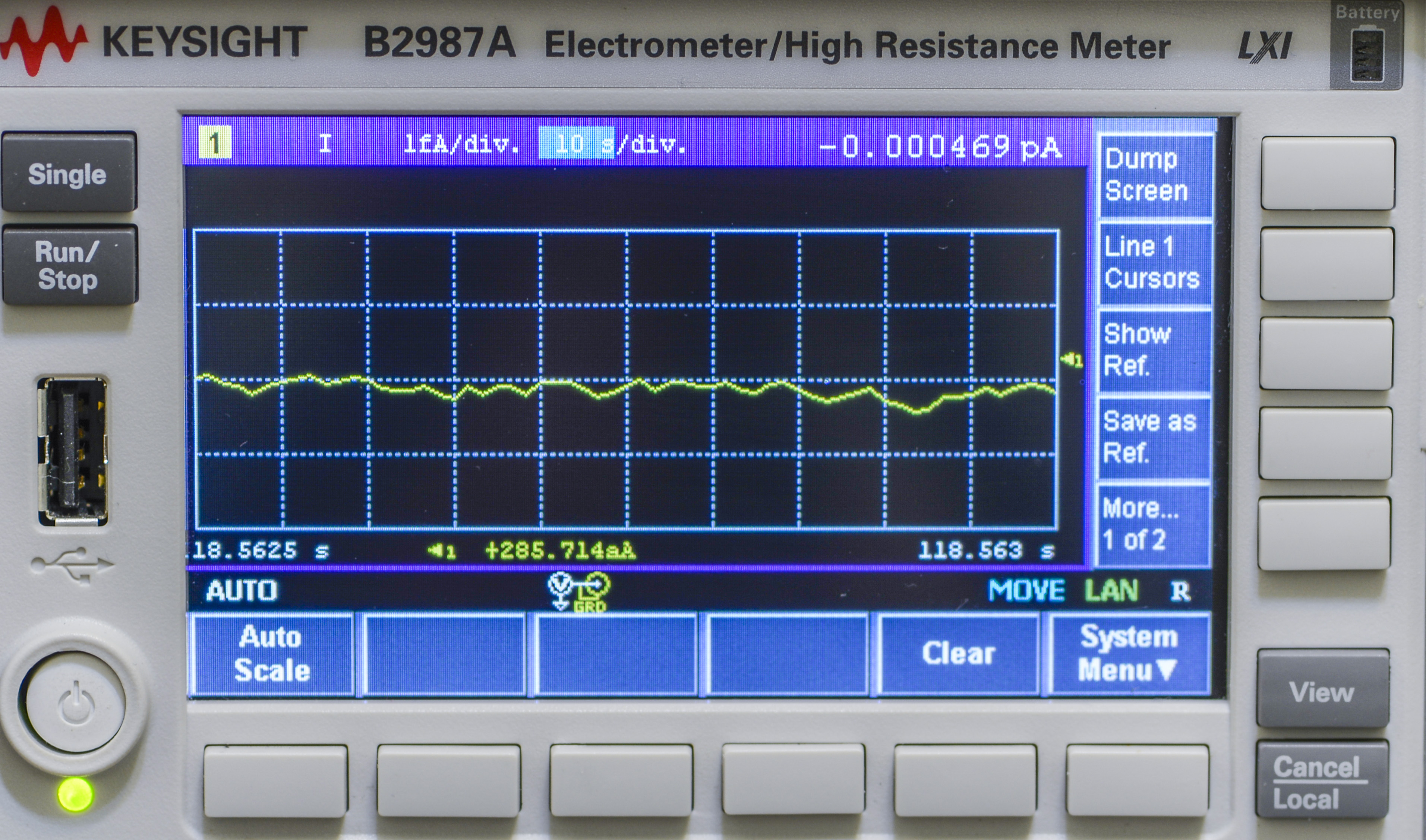
Image : test
1 Gigaohm resistance DUT prototype
To test and evaluate high-resistance measurement capability of B2987A special resistance standard prototype was assembled.

Image : 1 GΩ parts
It follows typical for such device design, with two isolated enclosures. Inner enclosure that contain resistor element driven by guard potential to prevent leakage and capacitance coupling to the outer shielded enclosure.
Isolation between inner guarded box and outer chassis-connected box also protects user from electric shock, as inner resistive element and guard can be driven up to 1000 V during the measurement.
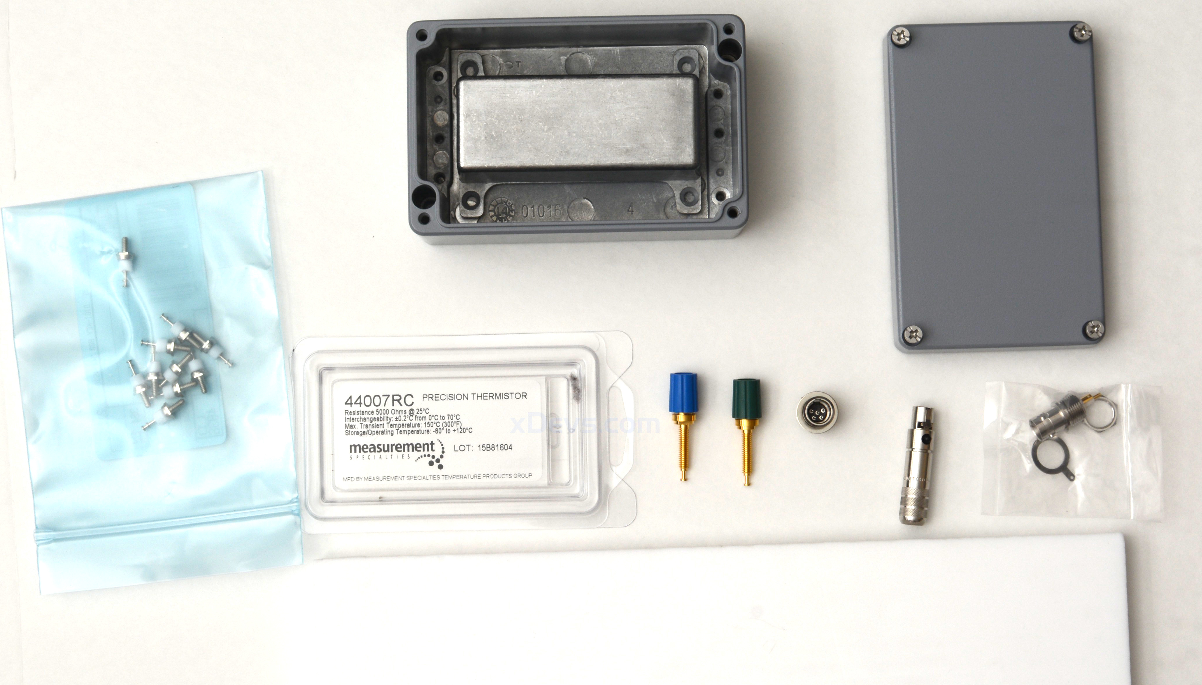
Image : test
Resistor terminals are floating so multiple measurement and use options are possible with our design. Connection interface is mixed set of triaxial 3-lug connector with inner shield tied to guard, and isolated BNC connected to other end of the resistor.
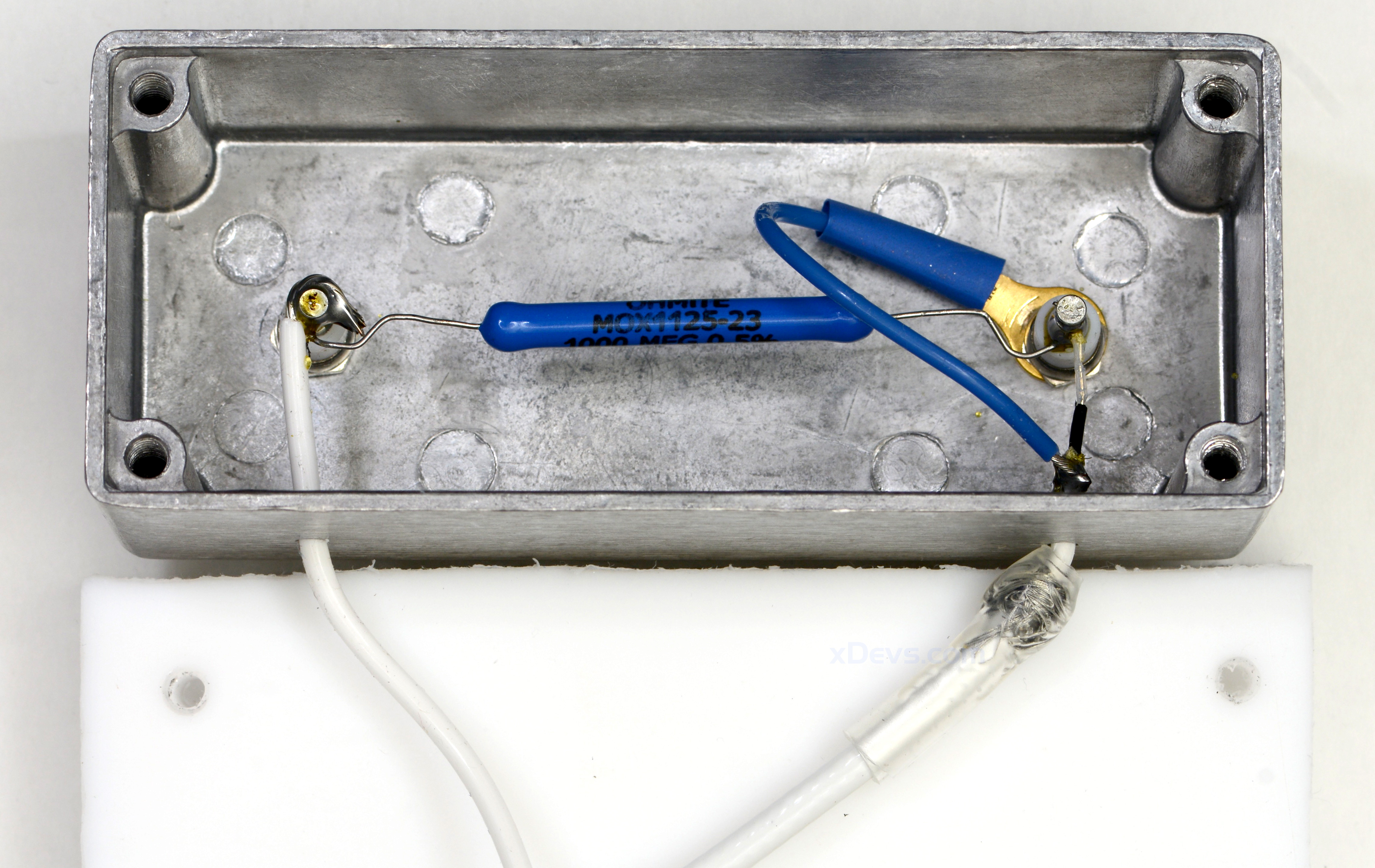
Image : test
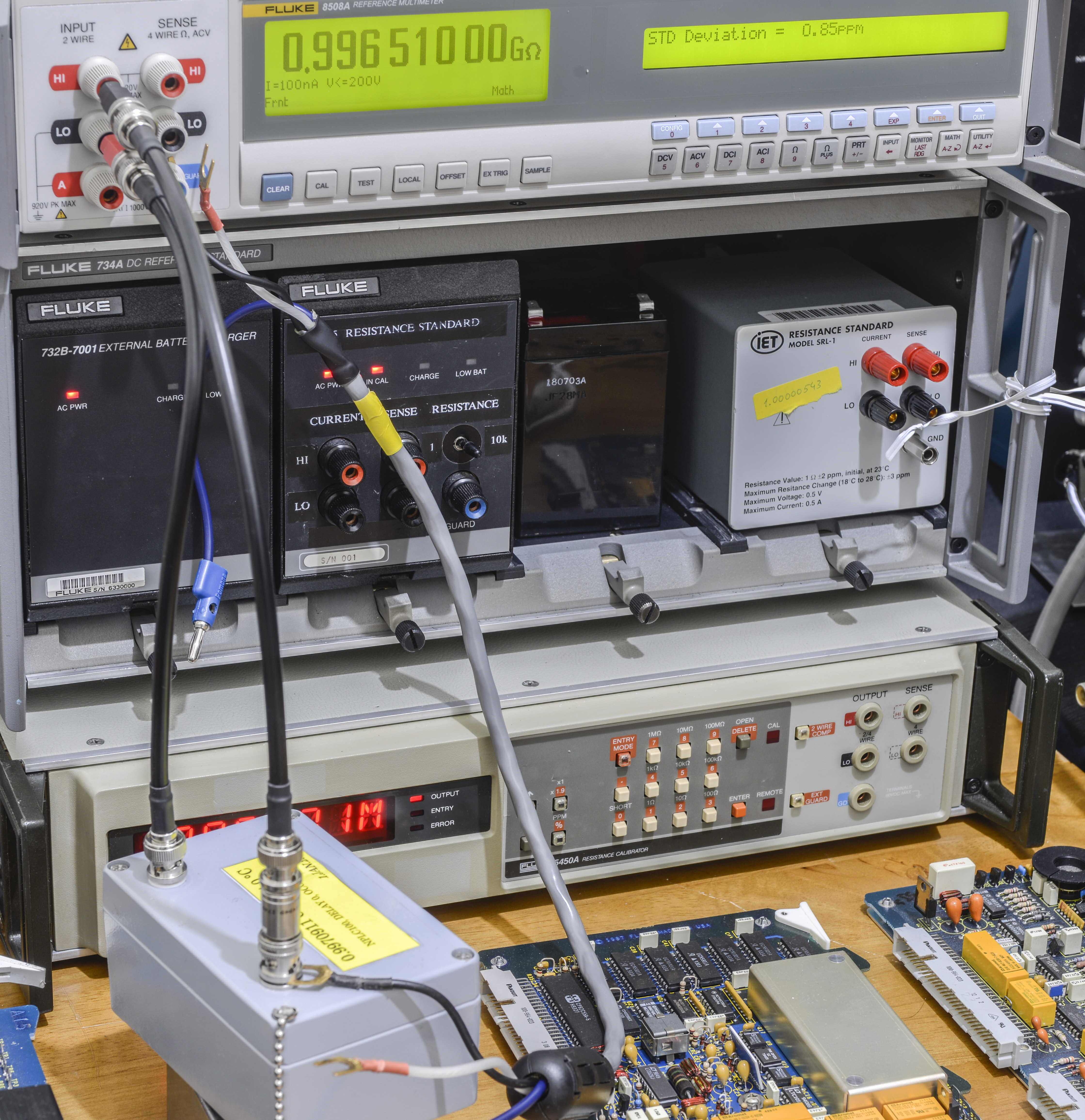
Image : test
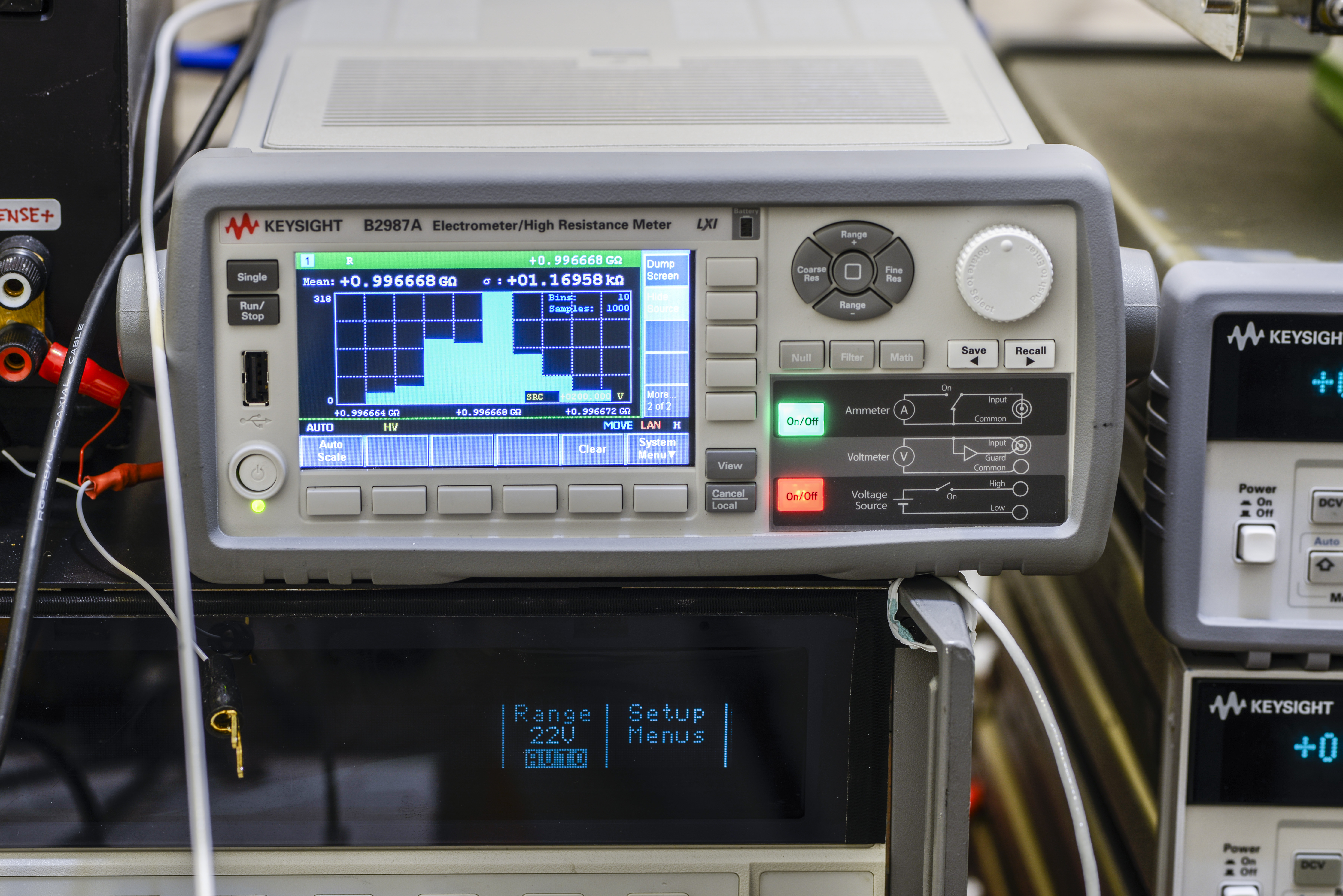
Image : 1 GΩ test
Connector leakage verification, using B2987A
Triaxial connectors as received. I expected to get triax ports with coaxial wire (often internal chassis ports connect shield of coax wire to guard only), but even wire is actual triaxial type. It is regular type triax, not low noise version however, which has graphite conductive layer between signal wire PTFE insulation and guard shield braid.
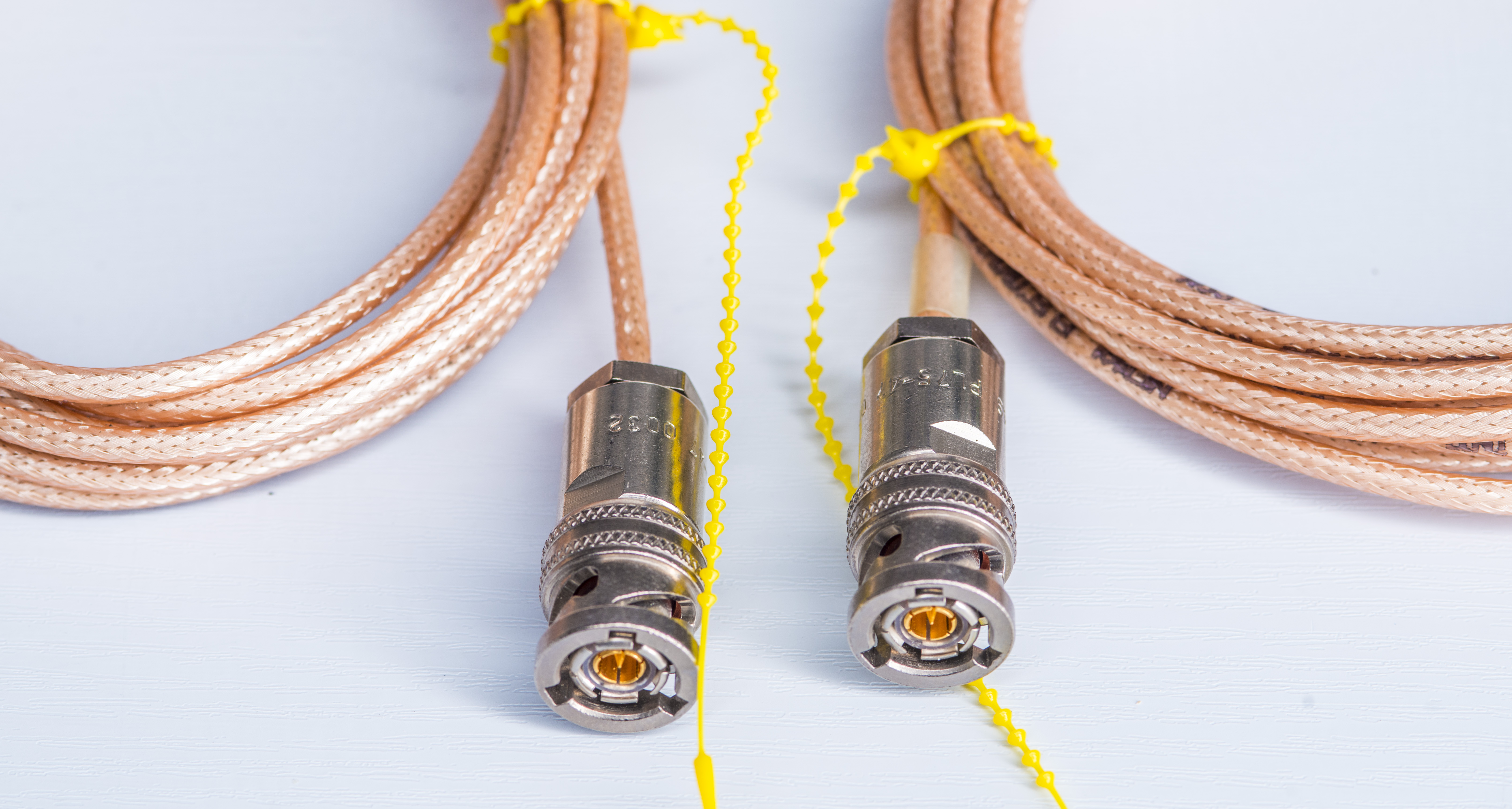
Seller also included pair of triax cables. They are nice cables, but not low-noise and rated for impedance 75 Ω, typical for Trompeter stuff for datavideo interfaces. Cable have printed marking “NEMAL ELECTRONICS INTL P/N 1729 TRIAX”. This suggests that manufacturer is NEMAL who specialize on audio/video equipment. Sadly, P/N 1729 search on their site did not reveal anything useful, perhaps it was a custom product for particular customer.

Here we can also see that center conductor soldered directly to triaxial pin, while guard and outer shield soldered with short green insulated jumpers. Whole thing covered with silicone-padded thermally shrink tubing. I have measured leakage of both triaxial cable wire and triaxial connector for few hours:
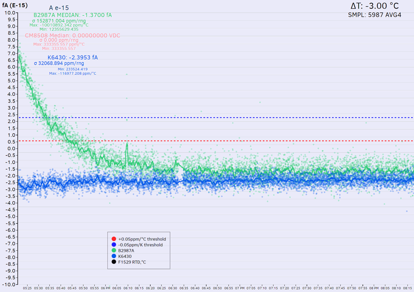
Keithley 6430 with preamp used to bias cable at 20V and measure leakage current at 2.0000 pA range.
Keysight B2987A used to bias connector with short piece of triax wire at 20 VDC, and measure leakage currents at 1.0000 pA range.
Both plots show settled current levels <3 femtoampere or <0.003 picoamperes, which at 20V applied translate into >6.6 PΩ resistance. It’s crazy high compared to nominal output levels of 5720A current output ranges. Even zero noise of calibrator is specified ±6 nA, which is way higher than this triaxial cable/connector leakage effects.
Discussion about this article and related stuff is welcome in comment section or at our own IRC chat server: irc.xdevs.com (standard port 6667, channel: #xDevs.com). Web-interface for access mirrored on this page..
Projects like this are born from passion and a desire to share how things work. Education is the foundation of a healthy society - especially important in today's volatile world. xDevs began as a personal project notepad in Kherson, Ukraine back in 2008 and has grown with support of passionate readers just like you. There are no (and never will be) any ads, sponsors or shareholders behind xDevs.com, just a commitment to inspire and help learning. If you are in a position to help others like us, please consider supporting xDevs.com’s home-country Ukraine in its defense of freedom to speak, freedom to live in peace and freedom to choose their way. You can use official site to support Ukraine – United24 or Help99. Every cent counts.
Modified: April 1, 2021, 10:16 p.m.