Intro
Main tool of most electronics hardware engineer is often an oscilloscope. Scope is your main eyes in device worlds, showing you what is actually going on your design. By comparing test result data with expected waveform, one can debug and trace issues and check important signal conditions. But what about firmware engineers, which work on complex multi-megabyte source codes for embedded systems? Oscilloscope in such case often useless, as data signals often not repetitive, come in long sequences, and probing wide interface such as parallel I/O or SDRAM memory bus would need lots of channels. It’s tedious work to trace and debug wrong byte in data dump of 5 millions of bytes using regular scope.
Dedicated logic analyzer come to address this case, and often are the main tool of firmware developers and digital design engineers. These devices operate similar to scope, but have tens or even hundreds of input channels available. Of course, this come at cost, so instead of capturing 8 or more bits of analog signal data, logic analyzer acquisition system triggers only on low or high signal levels, essentially behaving as very fast 1-bit ADC. Many LA’s have ability to adjust threshold level, supporting various I/O voltage levels and interfaces.
Let’s take a look on one example of such LA, old Tektronix TLA714, and do so in example of using it to debug SPI LCD issue.
SPI Interface
Few words about SPI first. There are many devices, chips, peripherals and instruments which use Serial Peripheral Interface or SPI. Be it your computer, smartphone or tablet which you use to read this article, SPI is used there to transfer bits of data in easy and transparent manner. SPI uses a duplex communication protocol with a master/slave architecture and separate select signals. SPI is known as a “de facto” standard. This means that there is no formal standard (in contrast to NXP’s I2C), and as such wide variation of implementations exist. It is common to find different clock speeds, word sizes, and variations with 2- to 5-wire interfaces using SPI protocol. These variations can cause a lot of debug issues, and cause extra engineering efforts.
Most common, 4-wire version of SPI uses a clock, two data (one for each direction), and a select signal. Some manufacturers refer this as a 3-wire interface, highlighting select line as separate from the clock and data lines. Not rare situation to have select multiplexes or controlled by extra logic to allow complex multi-device topologies.
The signal lines for SPI are defined as:
- Master Out Slave In (MOSI): Master device generates the signal, which is received by the Slave.
- Master In Slave Out (MISO): Slave device generates the signal, which is received by the Master.
- Serial Clock (SCLK or SCK): Master device generates the clock signal to sync data between the Master and the Slave.
- Slave Select (SSEL)/Chip Select (CS): Master device or glue logic generates the signal to select individual Slave devices.
SPI is capable of the fast speeds, up to 66-100Mbps and is capable of handling multiple slaves from a single master device. As throughput rates increase, considerations to the number of wires required by SPI and amount of devices on bus arise. The combo of configurations, along with the implementation variations and signal/timing integrity can rapidly become a complex test and debug task.
Test setup
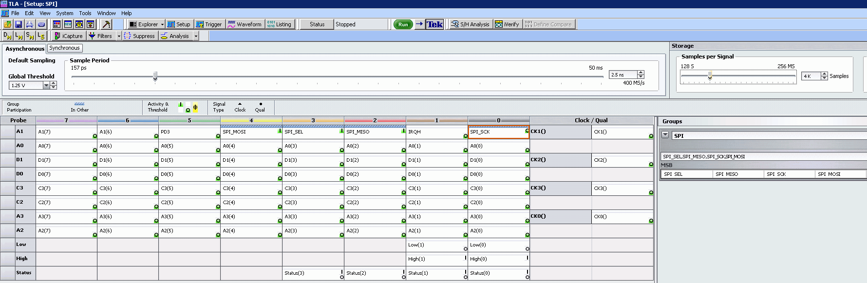
TLA714 have one 136-channel acquisition module installed, TLA7AA4 which we already covered a bit in this article. All four SPI signals from development board with test LCD were connected on inputs using one Tektronix P6860 probe.
LA software setup
Protocol decoder design for SPI data
https://dev.xdevs.com/issues/981
mingw32-g++ -Wextra -Wall -Os -Wno-unused -shared -o SPI.dll SPI.cpp
Usage:
- Copy to c:\Programm files(x86)\TLA 700\Supports\SPI
- Important to keep all filenames and folder name in Supports same
- Start TLA Application. Tested with 6.1.127 version running on remote controlled TLA714 (5.1 server app) + TLA7AA4 (5.8 module ver)
- Go Setup Window
- File>Load Support Package…
- Select SPI
- It loads default system, with SPI_SEL A0(7), SPI_MISO A0(6), SPI_SCK A0(5), SPI_MOSI A0(4). Group name and signal names are important!
- Order of signals in group is important! Correct is – SPI_SEL,SPI_MISO,SPI_SCK,SPI_MOSI and name of group SPI
- Set trigger and proper capture settings
- Capture signal
- Add column SPI Traffic if it’s not already there in Listing.
- Enjoy decoded packets view in Listing.
- Disassembly settings – Hardware – lowest level (all packets, start/stops), Subroutine highest level (only data)
First data capture
Transitional logic analyzer in TLA
Issue debug
Test system under scope had next topology:
Two Master devices are present on the bus, Controller A and Controller B, both in control of single Slave device, which is LCD module controller. One GPIO line from Controller A to Controller B is used to manage multi-master handling, so we can ensure that only one of controllers would try to access bus at a time. Both Controllers require to run LCD init code as display and Controller B allow surprise removal from main host.
Both master controllers can run initialize LCD code, and Controller A closed code firmware was developed by 3rd party. So we have no access to code and unable to see it’s LCD functions. If only test Controller B is used, no problems in LCD operation discovered, everything working as supposed.
Issue came when adding Controller A. LCD contrast setting get changed but it’s initialization code, resulting bad image display. By switching control over again to Controller B, LCD contrast can be set correctly. Logic analyzer is used to capture both data streams for Controller A and Controller B to find out root cause, why LCD is not working properly. Discovered information and test data result further provided to 3rd party vendor to correct their code and resolve the problem.
LCD resolution is 128×32 pixels, and each Controller init LCD and updates two frame-buffer images, so total more than 1024 bytes are send from each Controller, making analysis with regular scope or logic analyzer without transitional capture time-consuming. So 4-channel scope, even with MSO capability might make this debug bit time consuming.
Data analysis
Using TLA714 and decode library installed by procedure above, we can see screenshot of first data capture of initial SPI data stream. This covers initialization code from Controller A, which cause issue.
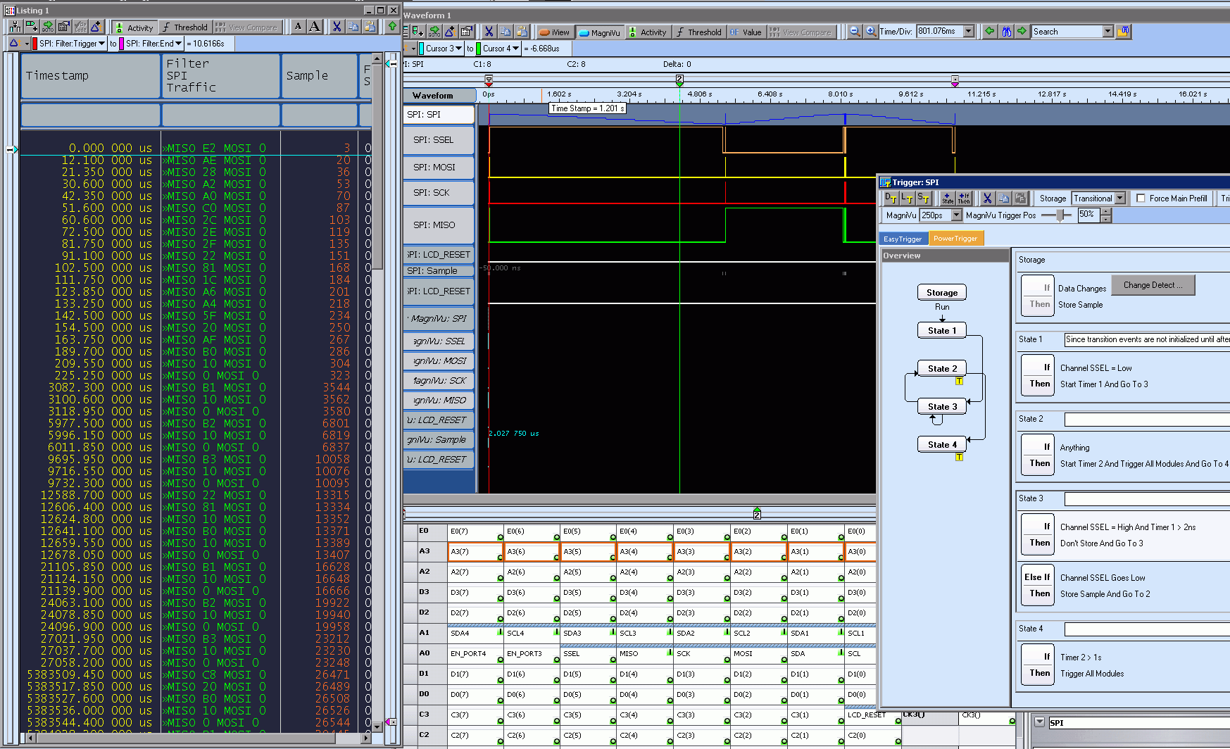
Initial setting and programming of LCD controller happens within first 30ms, followed by 5356 ms delay before next data packet group come.
Contrast setting configuration byte is 0×81 followed by next contrast setting data byte 0×1C. It takes just seconds to find out that first time correct contrast data is sent on timestamp 102.5us and 111.75us, as expected by reference initialize code.
But later this setting got overridden by repeating contrast setting databytes 0×81 and 0×10 on timestamp 12606.4us and 12624.8us. Thanks to easy view and decoded representation it was quick solution for specific problem case. Was it possible with oscilloscope or cheap USB LA? Yes. Would it be easy and quick like this? Perhaps not.
Example with SPI module loaded on TLA7BB2 module & TLA7012 system
Setup screen configured for SPI capture shown below. This particular example have next hardware connections to SPI device:
- Probe P6810 A1 bit 3 (orange) connected to SPI Chip Select
- Probe P6810 A1 bit 2 (red) connected to SPI MISO (Master In Slave Out)
- Probe P6810 A1 bit 0 (black) connected to SPI Clock
- Probe P6810 A1 bit 4 (yellow) connected to SPI MOSI (Master Out Slave In)
Files used for support module listed below. These files should be located under “C:\Program Files (x86)\TLA 700\Supports\SPI\” directory
TLA support system file for 7BB2 module
Also transitional PowerTrigger configuration available for download, if you want to capture only relevant SPI bit changed samples and not the fixed sample rate.
SPI PowerTrigger Transitional setup
Conclusion
Even though Tektronix TLA714 and TLA7AA4 used in this article are long obsolete and not supported, they are still useful for today engineers problems. Secondary market have plenty of these analyzers available in various conditions and prices, together with probes and support equipment. Of course there is a drawback to have large and bulky mainframe on your desk, but in many cases having one ready can save lot of time in complex designs. Benefit of such kit is also selective data storage compression (idle samples are not stored, not wasting precious sample memory buffer), advanced triggering and state machines and fast speeds available. I was able to debug and see signals on DDR3 1333MHz memory bus with TLA714 and TLA7AA4 module. Modern analyzer capable of such speeds would cost tens of K$USD.
I hope posted unofficial software module would help other owners to develop and share their own interface plugins, suitable for use in these old TLA7xx series machines.
Projects like this are born from passion and a desire to share how things work. Education is the foundation of a healthy society - especially important in today's volatile world. xDevs began as a personal project notepad in Kherson, Ukraine back in 2008 and has grown with support of passionate readers just like you. There are no (and never will be) any ads, sponsors or shareholders behind xDevs.com, just a commitment to inspire and help learning. If you are in a position to help others like us, please consider supporting xDevs.com’s home-country Ukraine in its defense of freedom to speak, freedom to live in peace and freedom to choose their way. You can use official site to support Ukraine – United24 or Help99. Every cent counts.
Modified: Jan. 11, 2021, 11:49 p.m.