Introduction
Perfect is the enemy of good. Also overspecification is often a problem in engineering and product management. Trying to obtain best of the best parameters can results in long schedules, large over-budget expenses and lost customers (because high cost or end product, or just missed timeframe). Successful products as result are often compromise between performance and cost/time to market. Different industry fields may tend to either bias on this two opposite scales in the spectrum, but it’s always there. Finding correct balance can be difficult challenge. I’ve learned this years ago, when trying to build the overspecified device without fixed dead line or money, such as KX calibrator source. Such undertaking require thousands of man-hours, and just not a right thing to start a project. Big companies like Fluke spent many years and needed teams of talented engineers to make high-performance calibrators. Same reason why we don’t see any modern startups trying to make competitive metrology products, such as calibrator or 8½-digit DMM. This market is just too niche and difficult to enter without decades of experience.
In electronics design it is often good idea to start with basic simple designs and after getting that working, improve on them and refine the performance as the end target application may need. There are no ideal components or circuits, but often practical applications can deal and workaround from reasonable performance/cost budgets. Same applies to precision calibration equipment, such as DC Voltage sources. This is number one tool for testing voltmeters, ADCs, DACs and various analog circuits. There are many products suitable for this task, some simple like fixed zener reference or DAC chip, some are more elaborate precision calibrated sources like EDC MV106 or commercial high-end metrology calibrators, such as Fluke 5720A. Cost of these solutions occupy span from 1-10 to hundreds of thousands USD.
Here we often experiment with and repair old high-end DMMs and instruments. Many of these repairs would not be possible without some kind of stable DC Voltage source, such as calibrator or programmable DAC system. This case is not unique to our needs, and other electronics designers also have similar requirements. One of such engineers, Ian Johnston who worked in electronics design field professionally since 1984 spend lots of hours doing analog, digital and uProcessor based designs. In about 2011 he created electronics workshop and worked on a few hobby-type projects and repairs. Eventually, he shared experiences on YouTube channel and have fun there doing mostly repairs, and sharing his knowledge with community.
Through all that repair work Ian reached at the need a small adjustable, portable voltage source, but without large pricetag. He made a simple analog one with few op-amps, battery and a adjustable potentiometer. Once that was working he was already working with modifications for an EDC Programmable DC Voltage Standard. Then using Arduino’s in various home projects it was an obvious step to bridge the Arduino together with a Precision DAC just to build precision DAC source for himself.
So he made three prototypes of such DC source and sent one to Dave Jones @ EEVblog mailbag for fun. Dave’s words were “Ian has got to make these”… So that’s how PDVS1 hobby small-scale production DC Voltage source was born, using LM399AH reference and controlled DAC. PDVS2 was a improved version and progression of the PDVS1 with additional functionality like rotary encoder, backlight and battery charging.
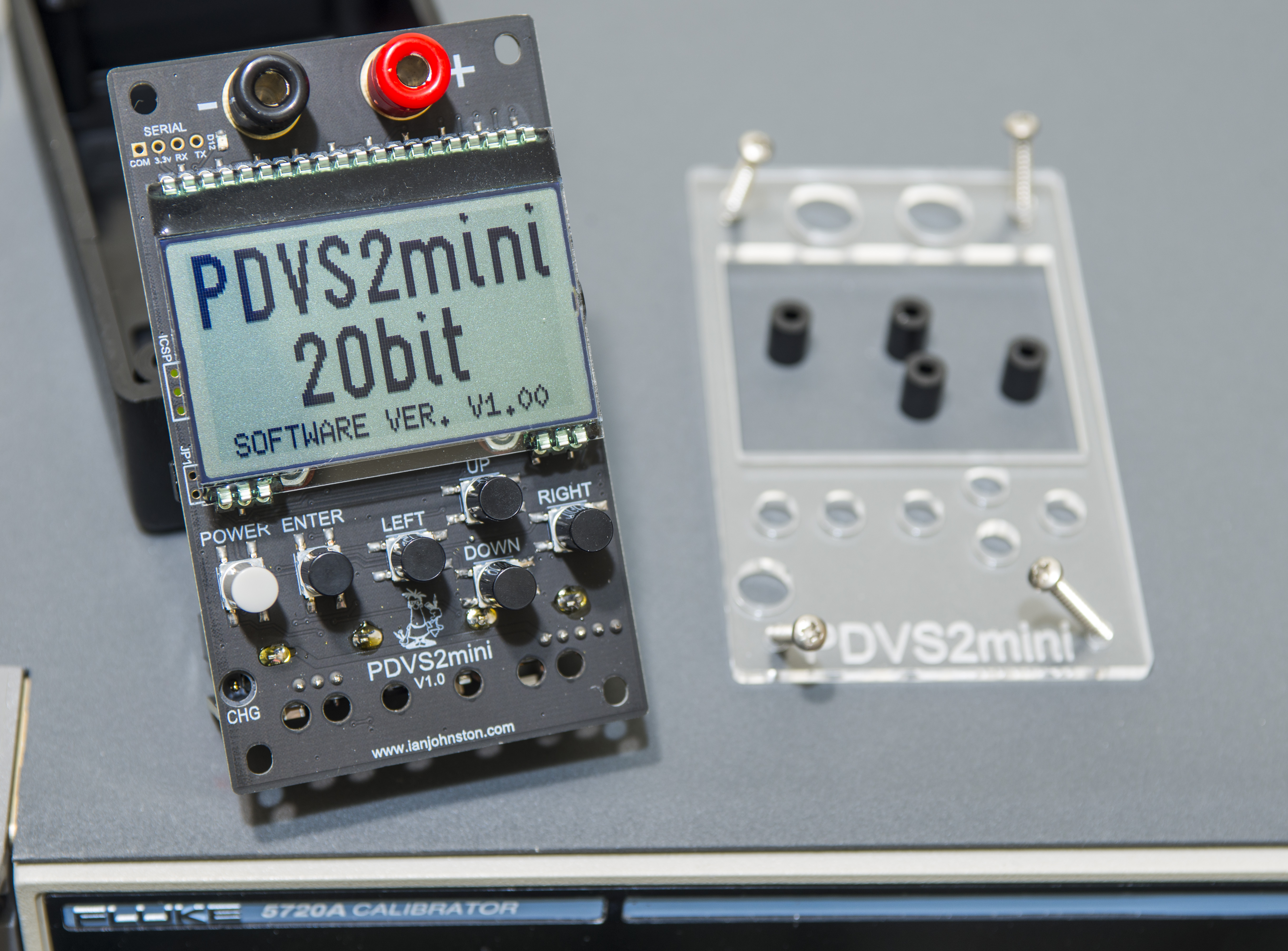
PDVS2mini is his third iteration at the DC Voltage Source, this time lower-cost version of older PDVS2 design, yet with some improved specifications. Ian sold quite a number of original PDVS2 units, but many hobby-type customers were still asking for more affordable unit. Ian optimized BOM and worked out ways to make it not only cheaper, but also increase the resoloution to 20 bits (PDVS2 has 18 bits DAC) at cost of lower spec (INL, stability).
PDVS2mini key feature set:
- 0 VDC to 10 VDC user adjustable output (5½-digit resolution in approx. 10uV steps)
- Soft-power switch to save battery power
- Industry known LM399AH ovenized voltage reference
- 20-bit Maxim MAX5719A Voltage DAC, ± 32 LSB INL
- Battery voltage monitor, including low voltage warning, auto-shutdown and charging status
- 2.4” Graphics Monochrome LCD (128×64 pixels)
- Atmel AVR ATmega1284 micro-controller (uses Arduino bootloader)
Disclaimer
Redistribution and use of this article or any images or files referenced in it, in source and binary forms, with or without modification, are permitted provided that the following conditions are met:
- Redistributions of article must retain the above copyright notice, this list of conditions, link to this page (https://xdevs.com/article/pdvs2mini/) and the following disclaimer.
- Redistributions of files in binary form must reproduce the above copyright notice, this list of conditions, link to this page (https://xdevs.com/article/pdvs2mini/), and the following disclaimer in the documentation and/or other materials provided with the distribution, for example Readme file.
All information posted here is hosted just for education purposes and provided AS IS. In no event shall the author, xDevs.com site, or Ian Johnston or any other 3rd party be liable for any special, direct, indirect, or consequential damages or any damages whatsoever resulting from loss of use, data or profits, whether in an action of contract, negligence or other tortuous action, arising out of or in connection with the use or performance of information published here.
If you willing to contribute or have interesting documentation to share regarding pressure measurements or metrology and electronics in general, you can do so by following these simple instructions.
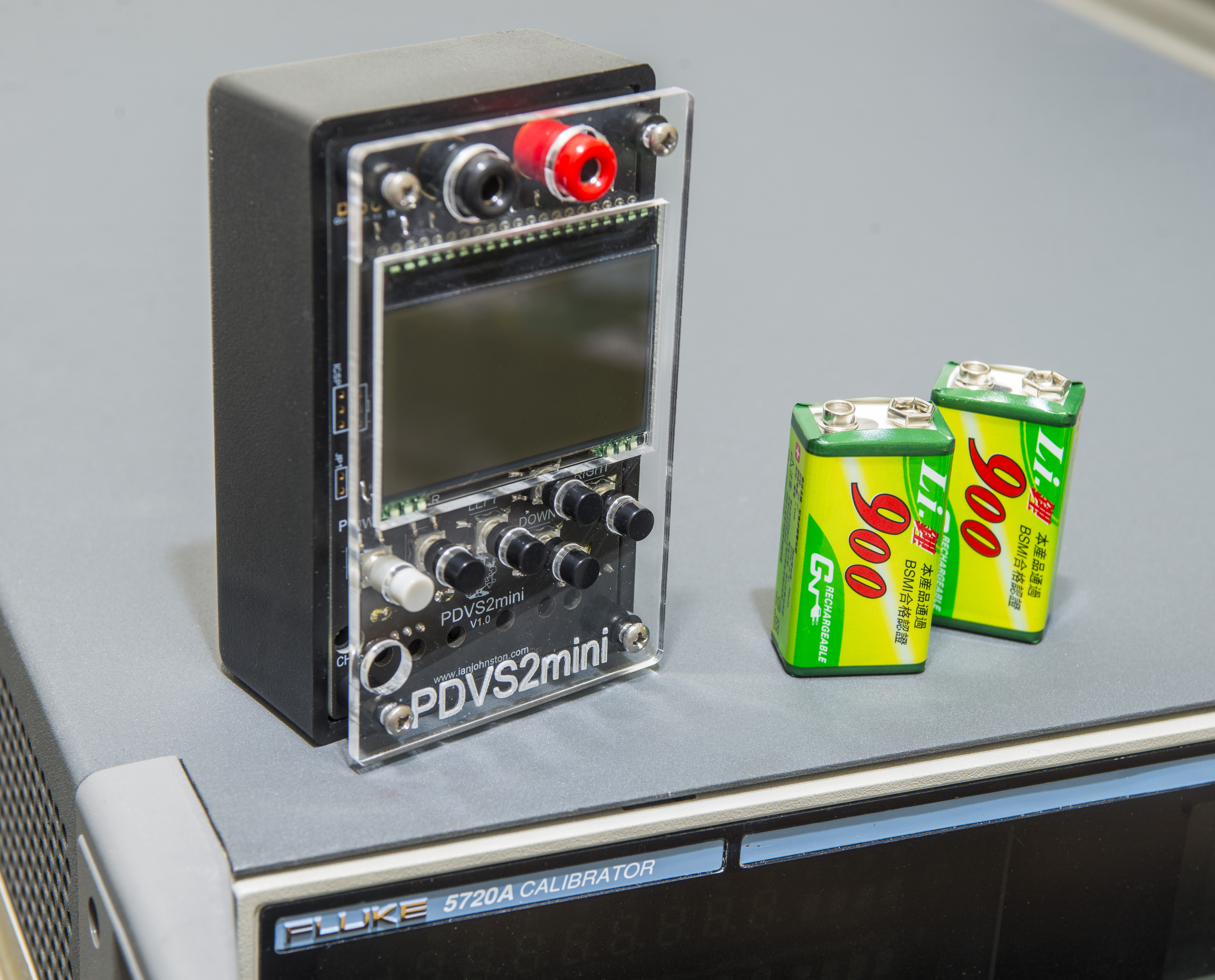
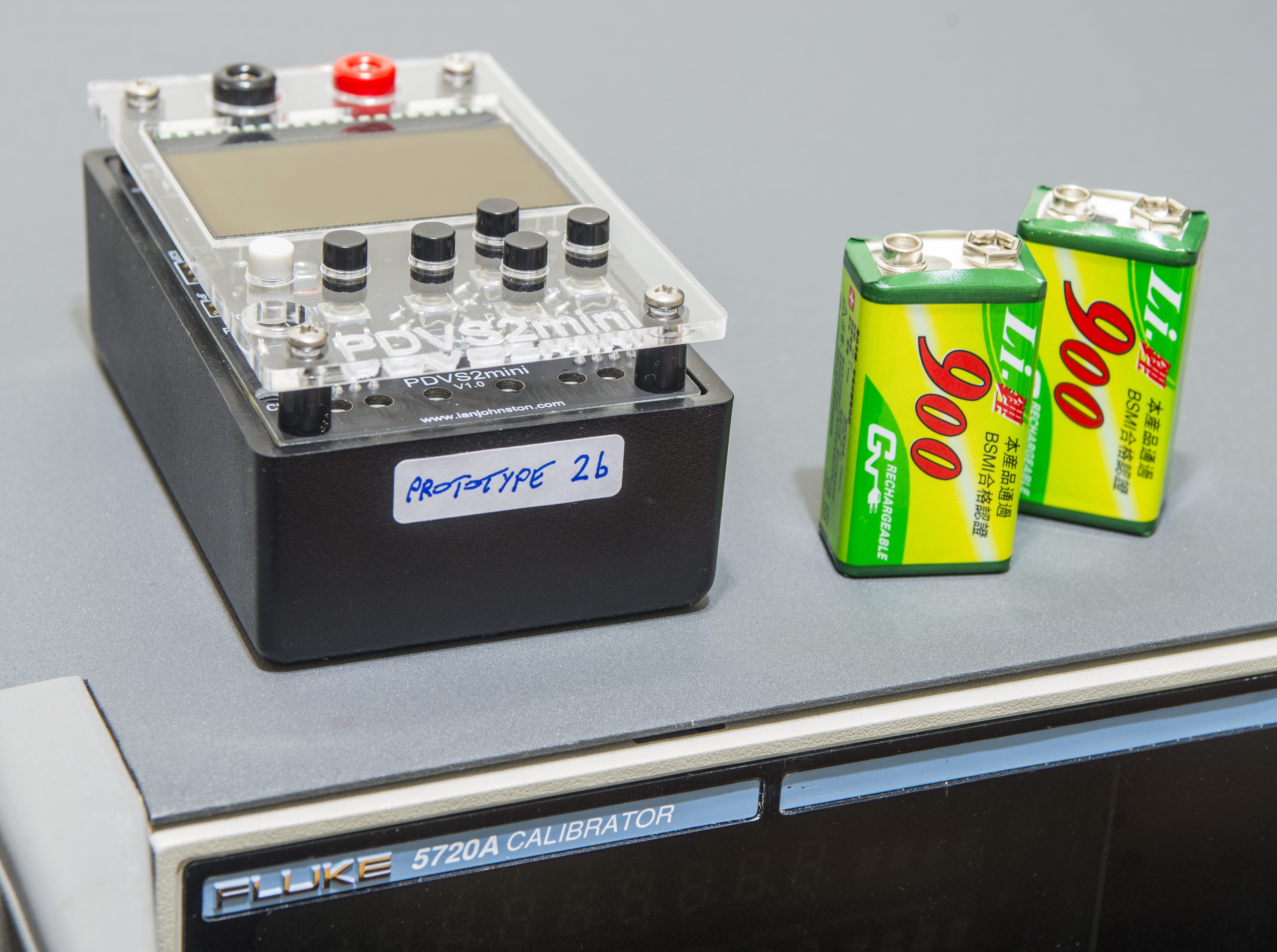
$300 PDVS2mini sitting on top of $70000 Fluke 5720A 7½-digit multifunction calibrator. They both can do same thing, which is source precision DC voltage.
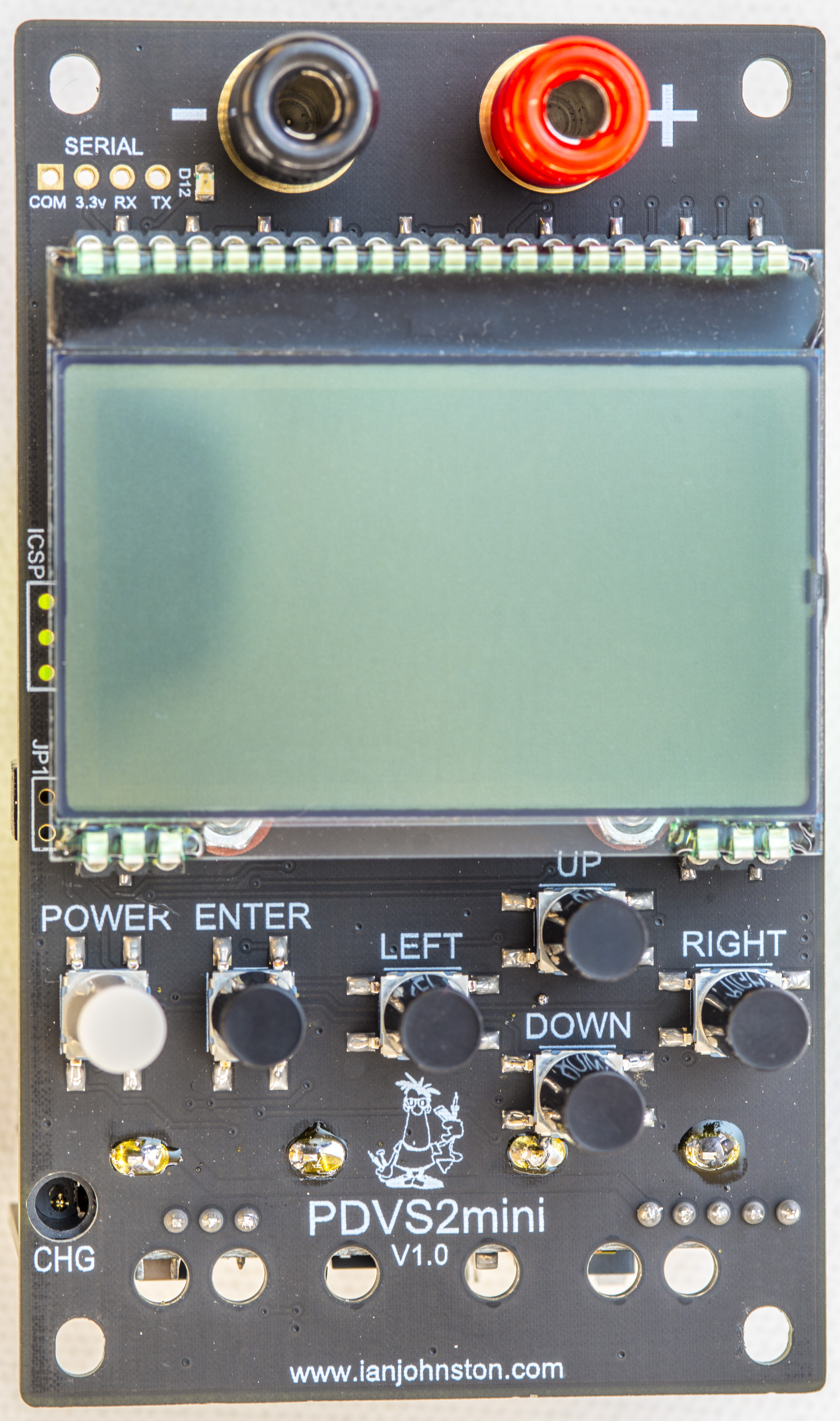
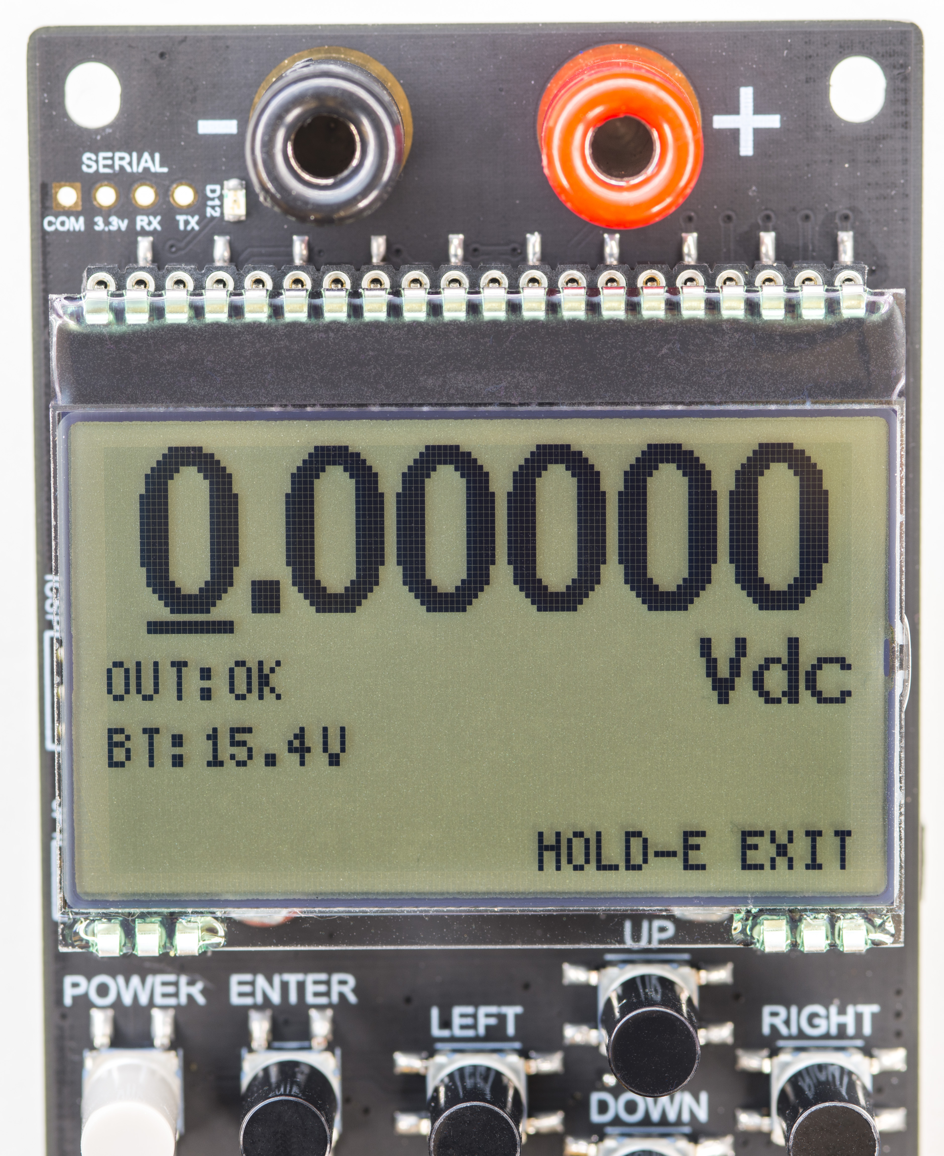
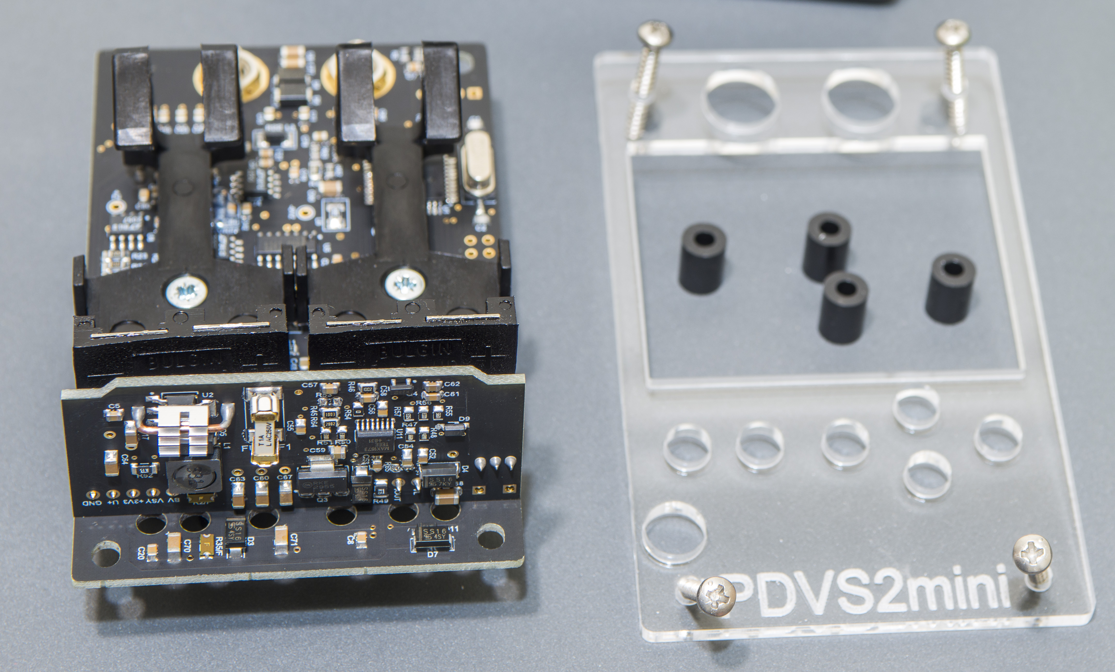
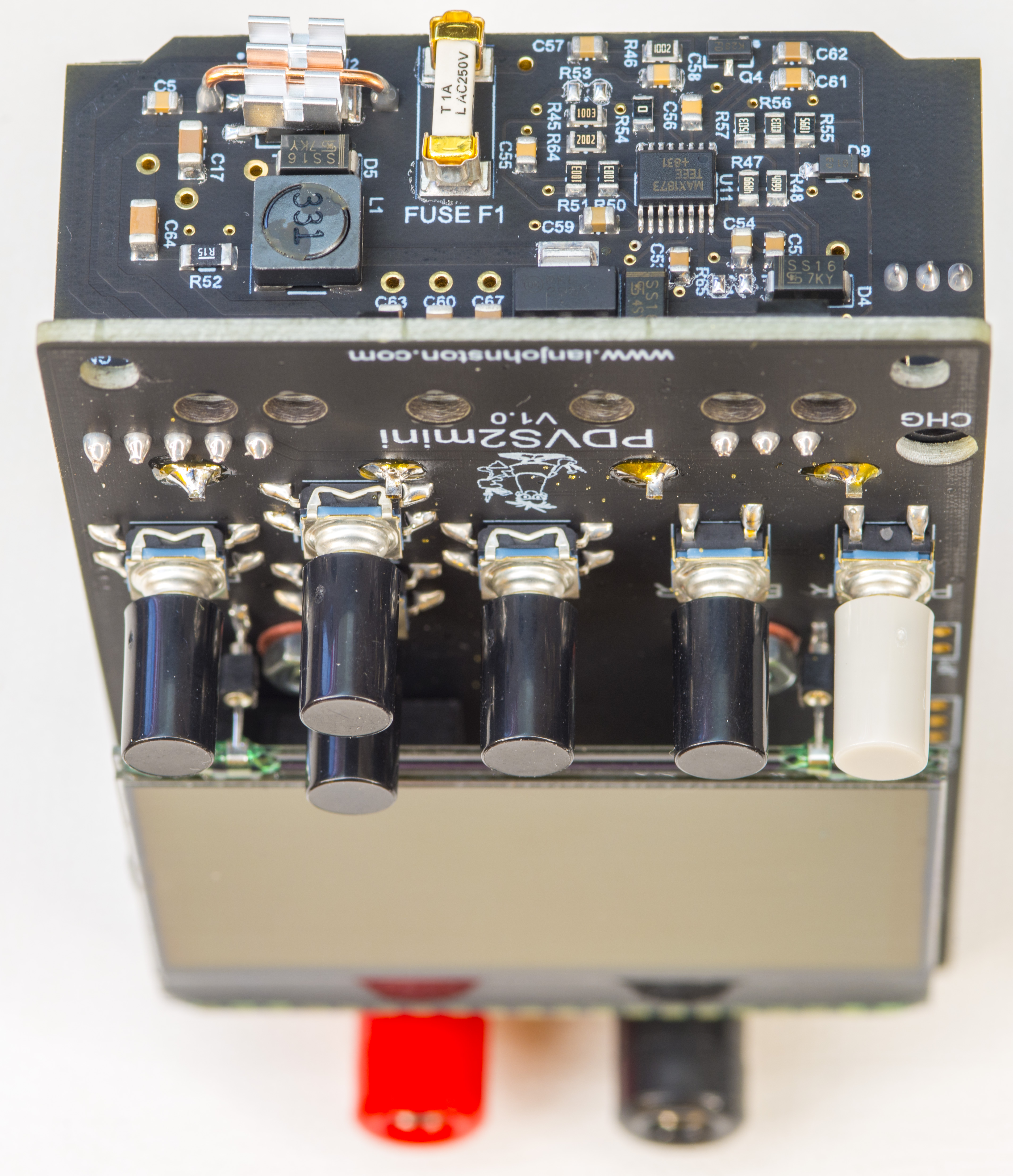
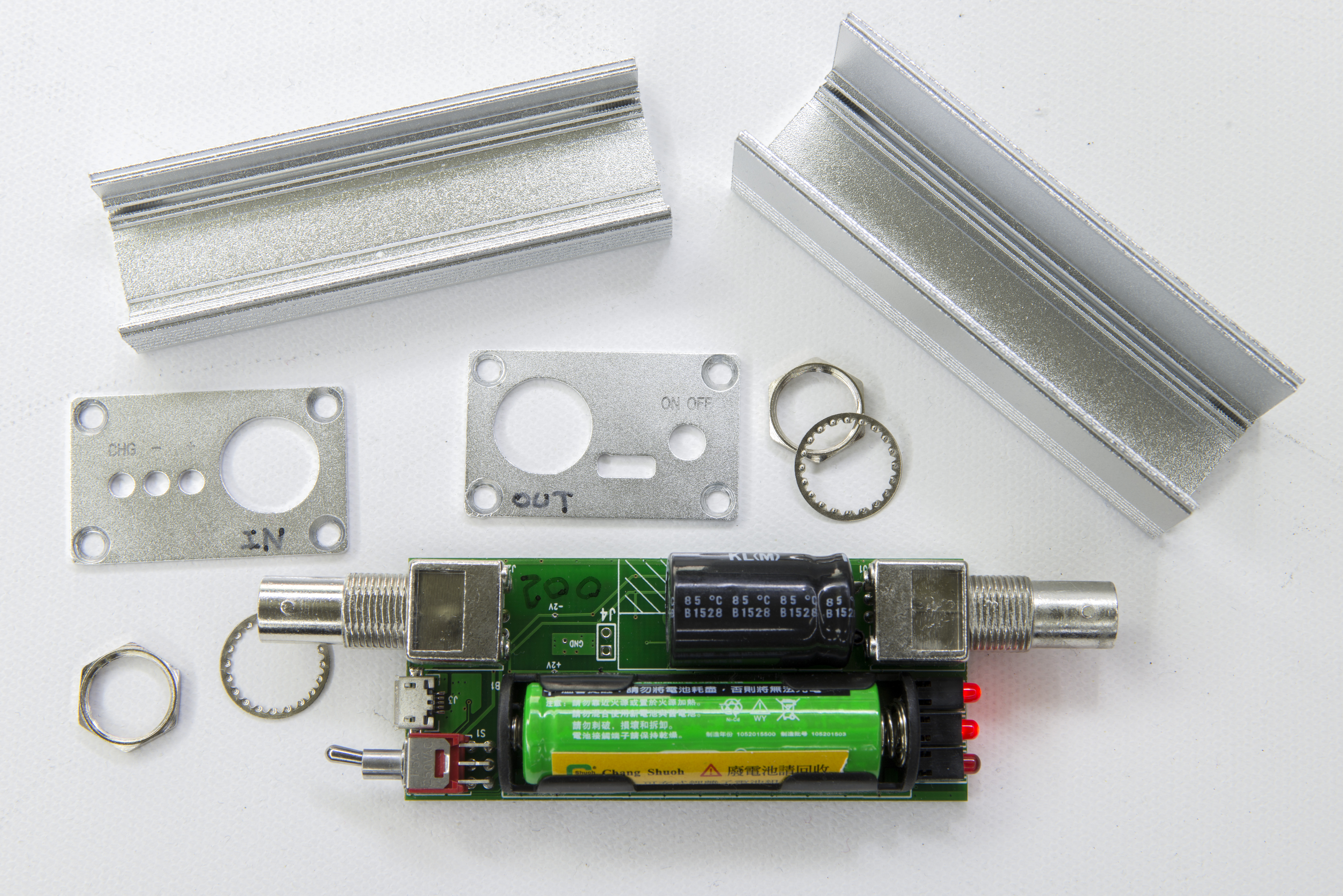
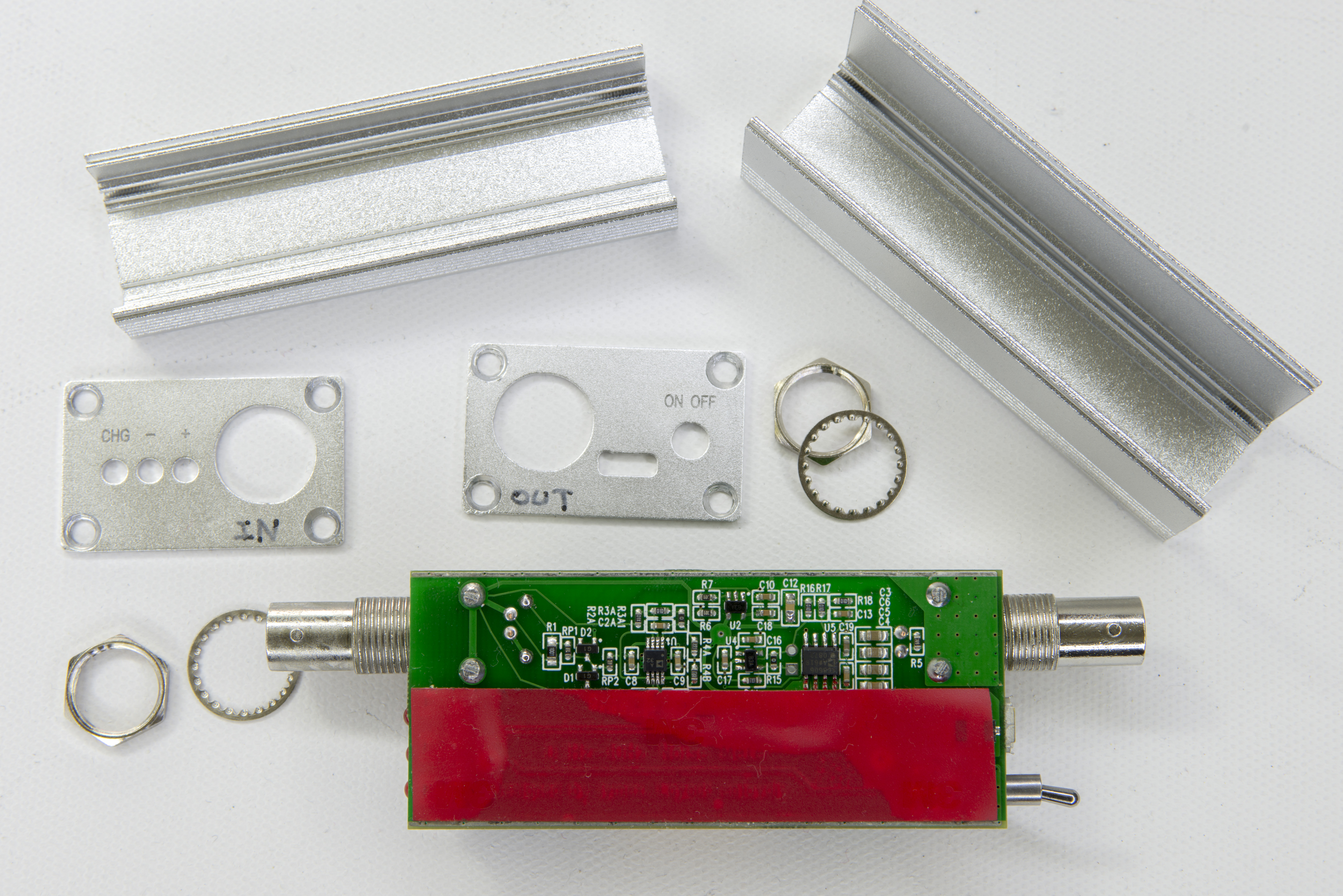
Design assembly is nice and tidy, with all critical stuff well cared. Graphical LCD is not backlit, just COG panel. It has decent contrast and main output voltage have nice large digits. The menu system is little unusual but not hard to figure out without any RTFM. There is a help string on the bottom strings to show keypad actions.
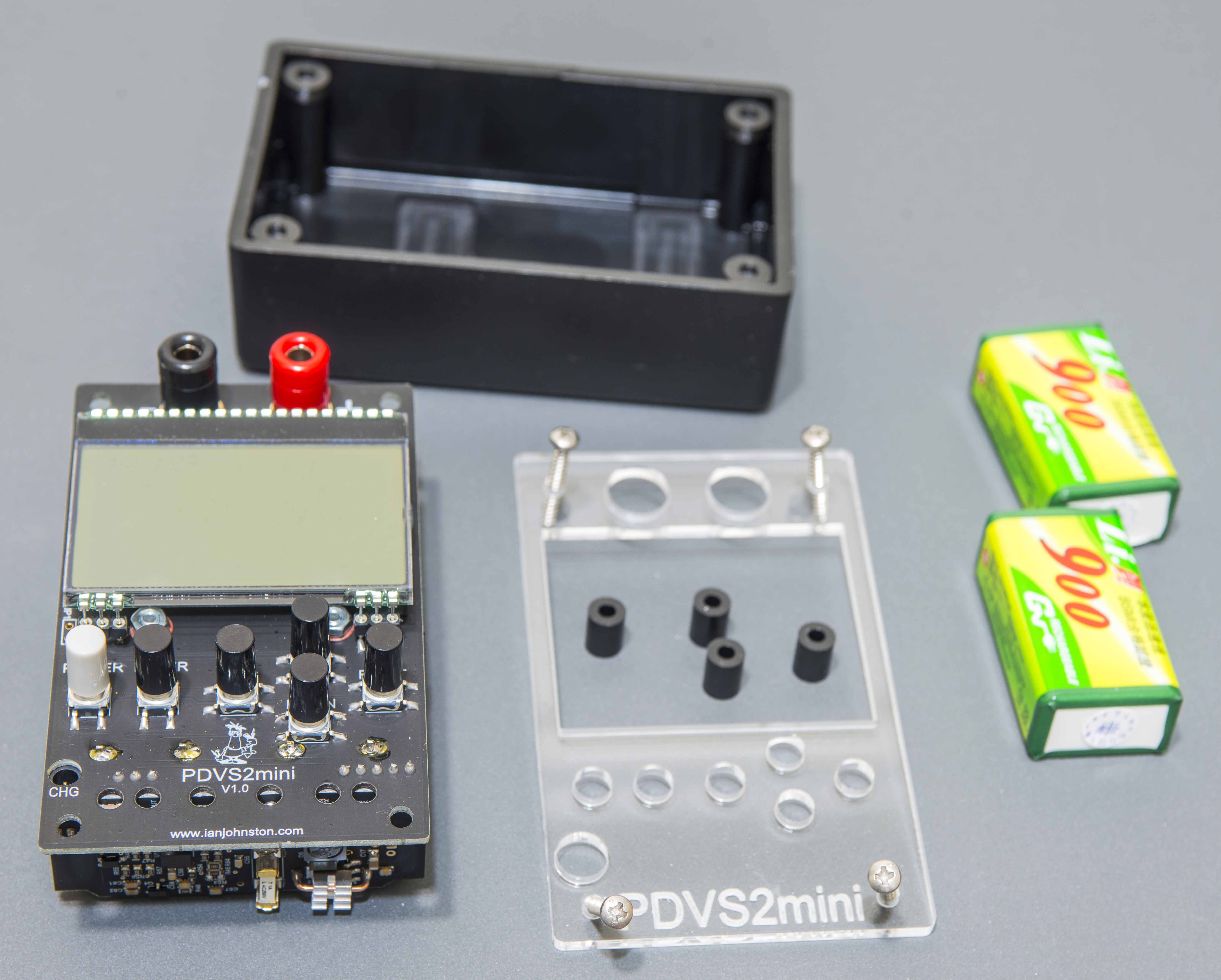
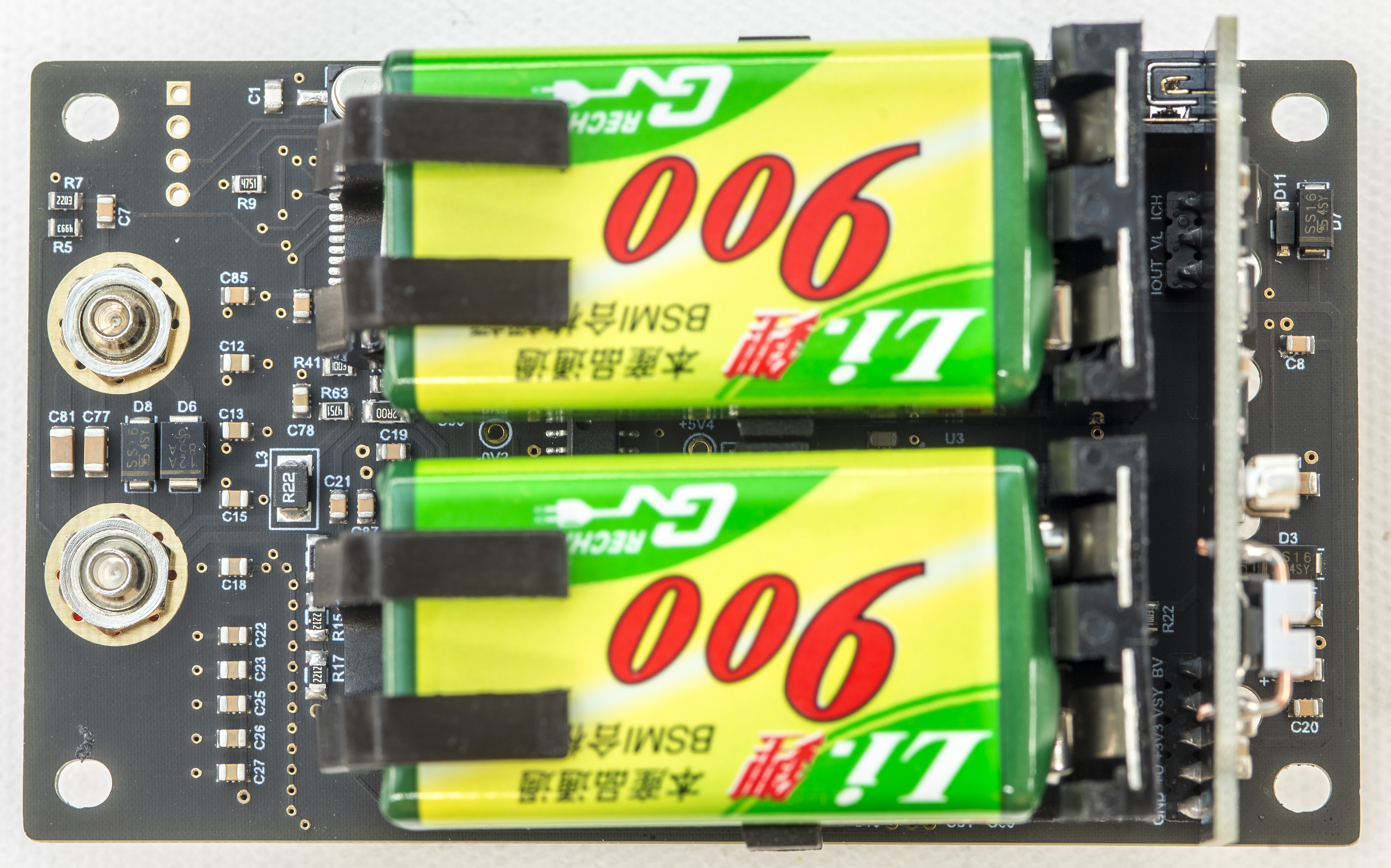
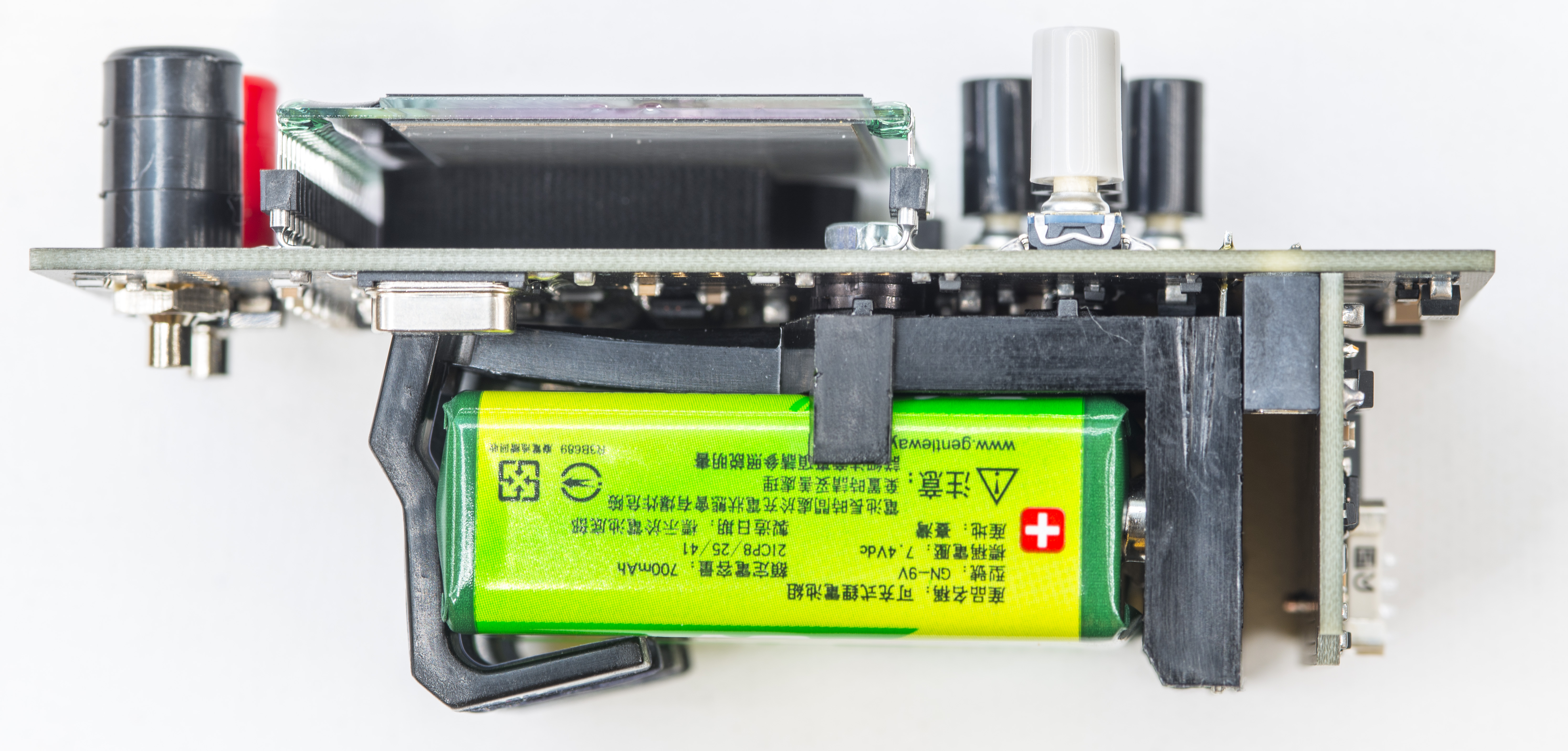
Access to battery requires removal of 4 screws, and also provide a way to see some internal construction. There is no separate battery compartment or protection over electronic parts, due to low-cost targeting reason, which is understandable. PDVS2mini designed to use two 9V batteries in series, with integrated charger. Unit needs to be powered on to allow charging from external DC jack.
Performance verification
Temperature stability
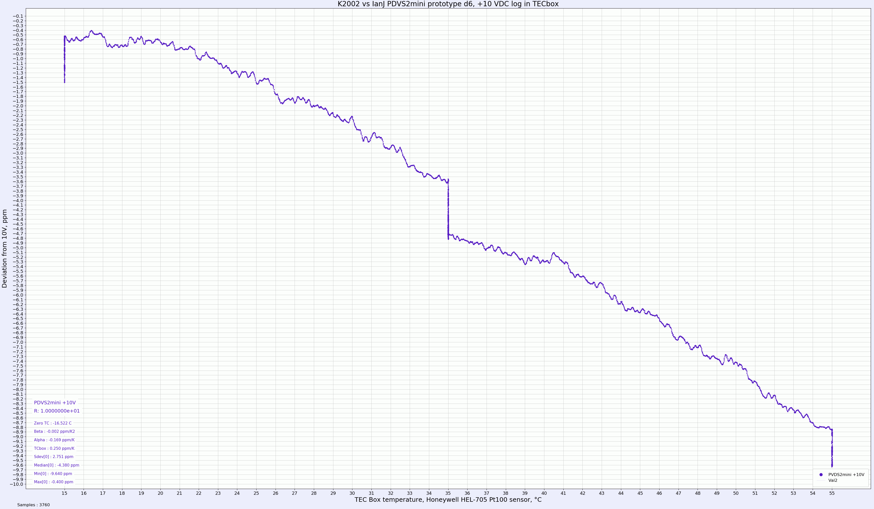
Here’s quick test of temperature coefficient (deviation of the output voltage from desired programmed value, due to ambient temperature change) of the DC output. PDVS2mini was programmed to fixed +10.0000 VDC output and placed in small airbath temperature chamber, equipped with TEC element. Temperature inside the chamber was controlled by Arroyo 585 TECpak, with 0.02 °C resolution and stability better than 0.008 °C over hours.
The first graph is a plot of +10V output from PDVS, with temperature change from +15.00 °C to +55 °C in a slow and controlled manner. There is soaking time at +35°C for 2 hours, and also at peak max temperature, to get an idea of settling and hysteresis behavior. The horizontal axis is time duration, vertical axis is deviation from initial point at +15 °C, which happened to be +9.999994 VDC +/-2ppm.
For illustrative purposes, chart have additional plots of -0.1 ppm/°C and -0.2 ppm/°C thresholds based on temperature change (using box method) and TEC current readout from Arroyo TECpak 585. Ramp up time for temperature is +0.08333 °C per minute. Measured deviation is -4.0 ppm for +15.0 °C to +35 °C ramp, and another -5.3 ppm for +35 ° °C to +55 °C ramp. Following the TC Box method we can estimate temperature stability at max -0.23 ppm/°C which is impressive for $300 USD DAC box!

Image 3: PDVS2mini +10.0000 VDC TC +15 to +55 °C. Raw DSV-formatted file .
Now same data, but in voltage/temperature scale representation. This particular temperature chamber does not use forced airflow, and from datalog looks like it need ~30 minutes to equalize temperature change. This effect is visible as vertical line at fixed +15, +35 and +55 °C setpoints.
Noise test benchmarks
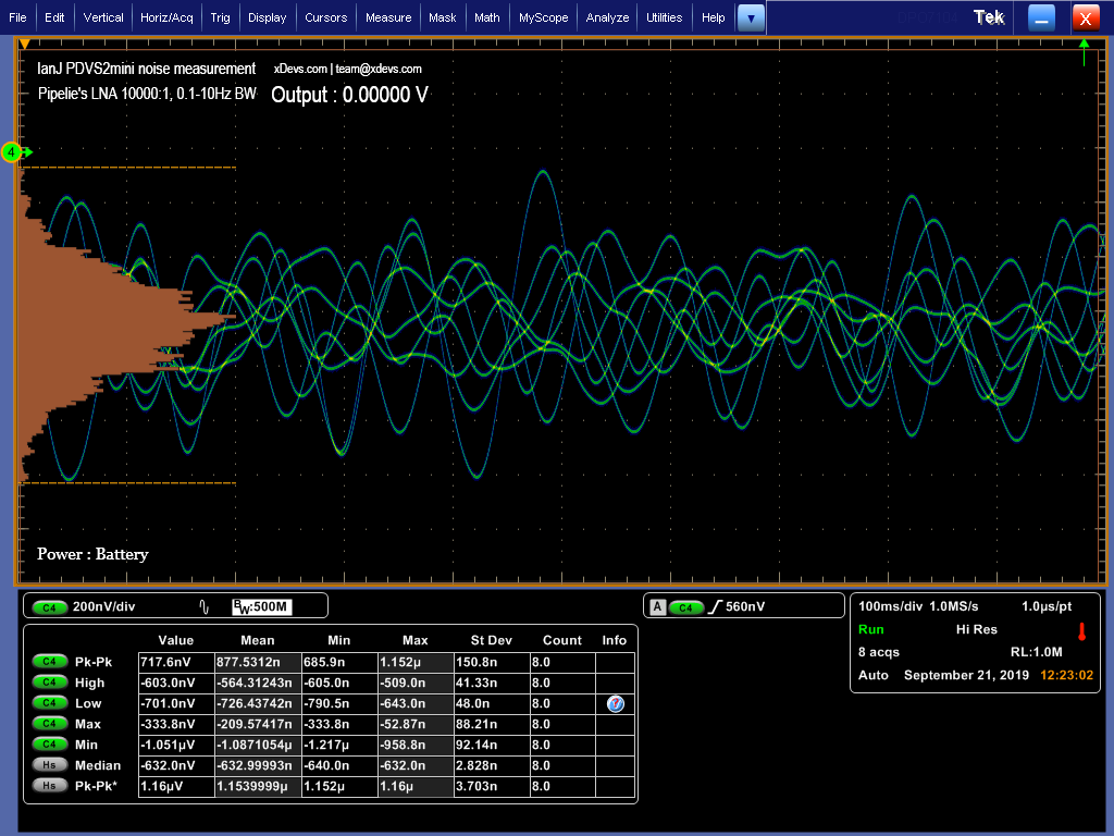
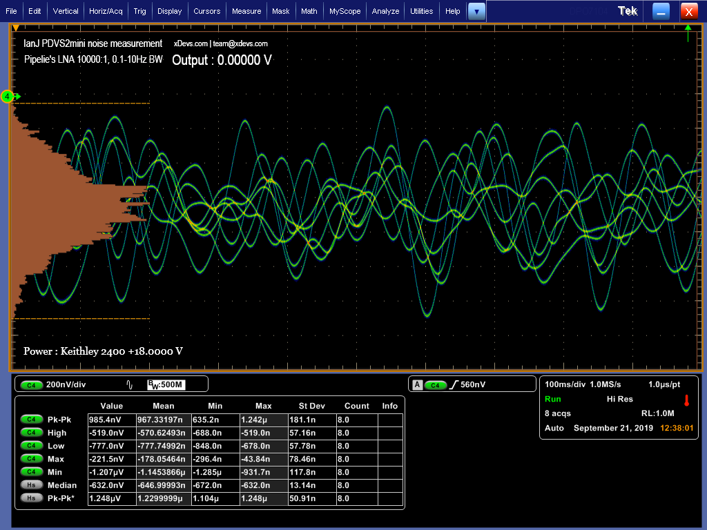
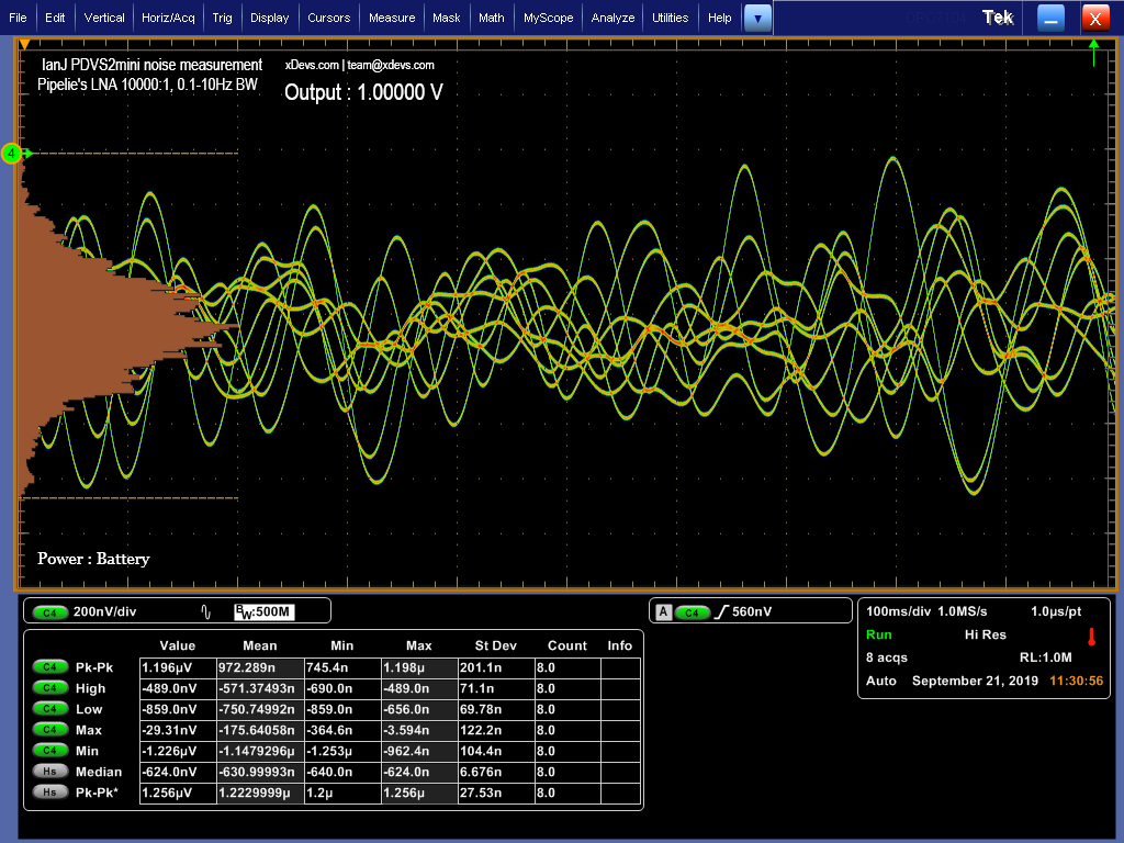
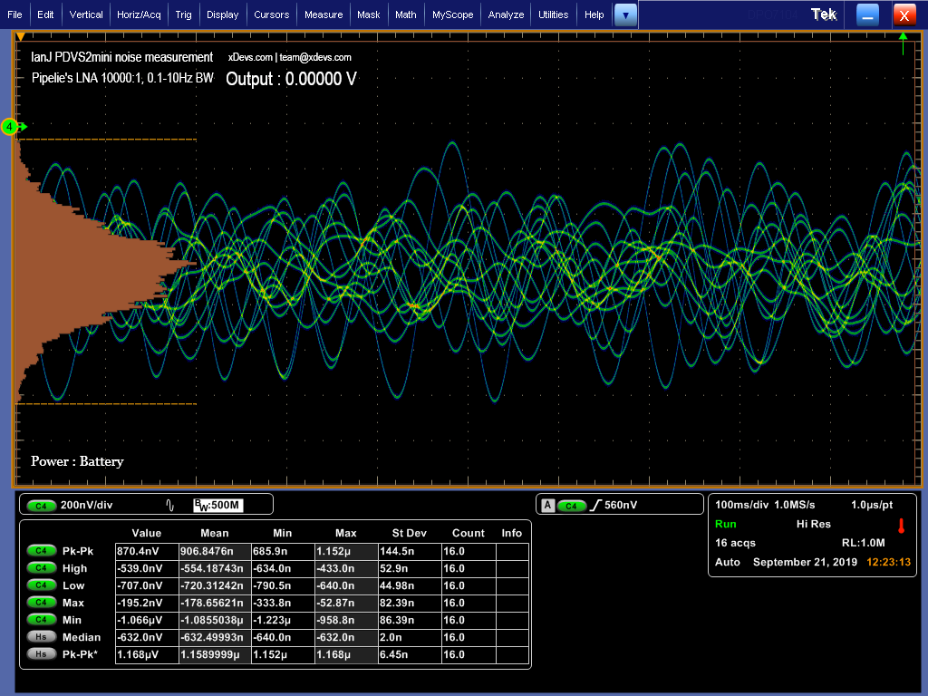
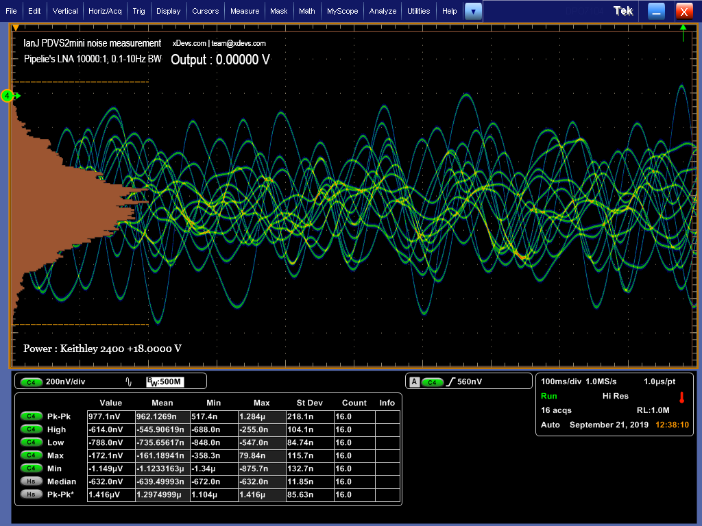
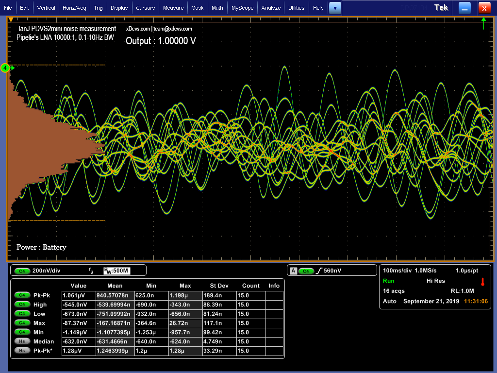
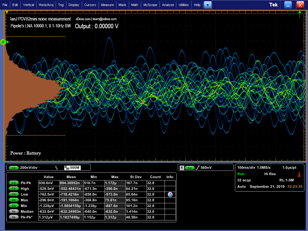
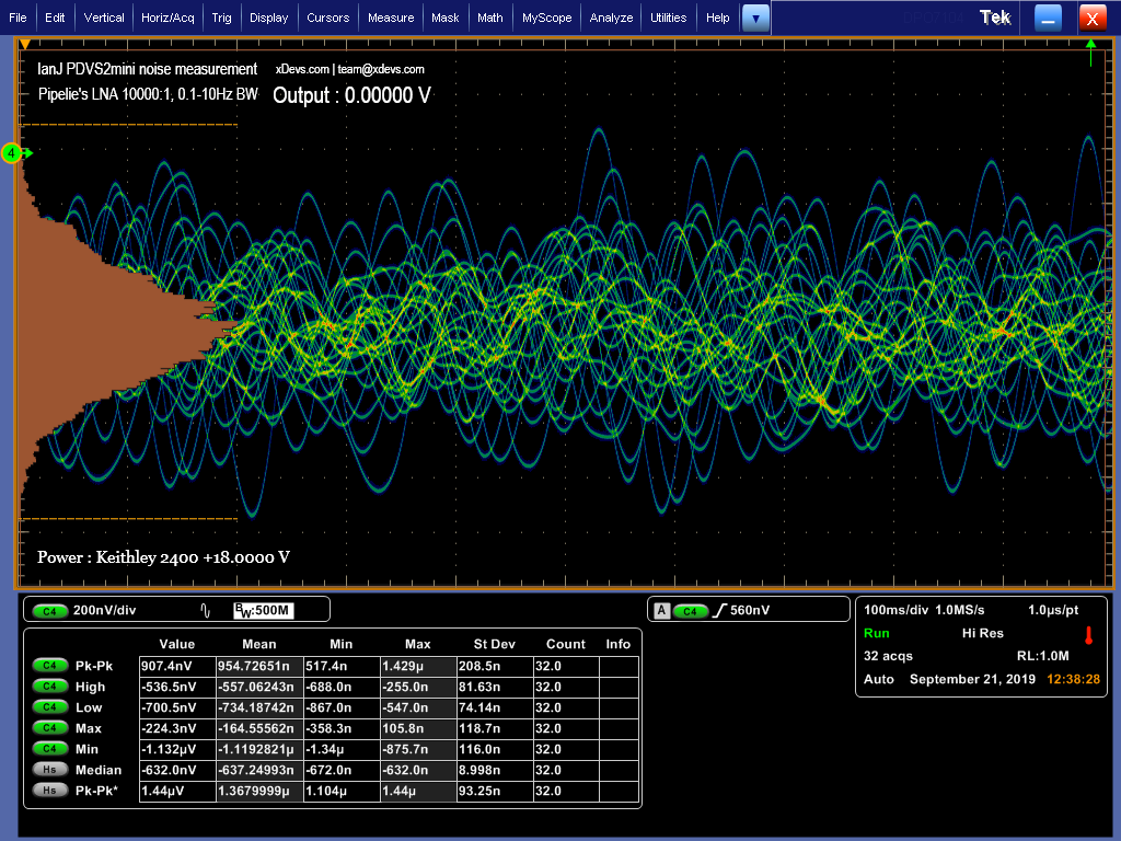
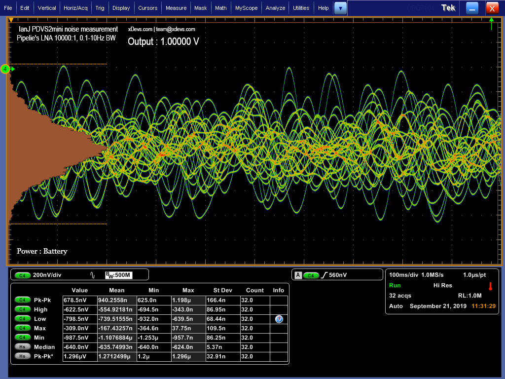
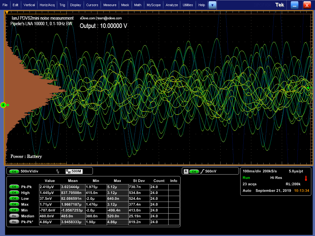
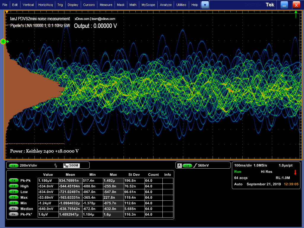
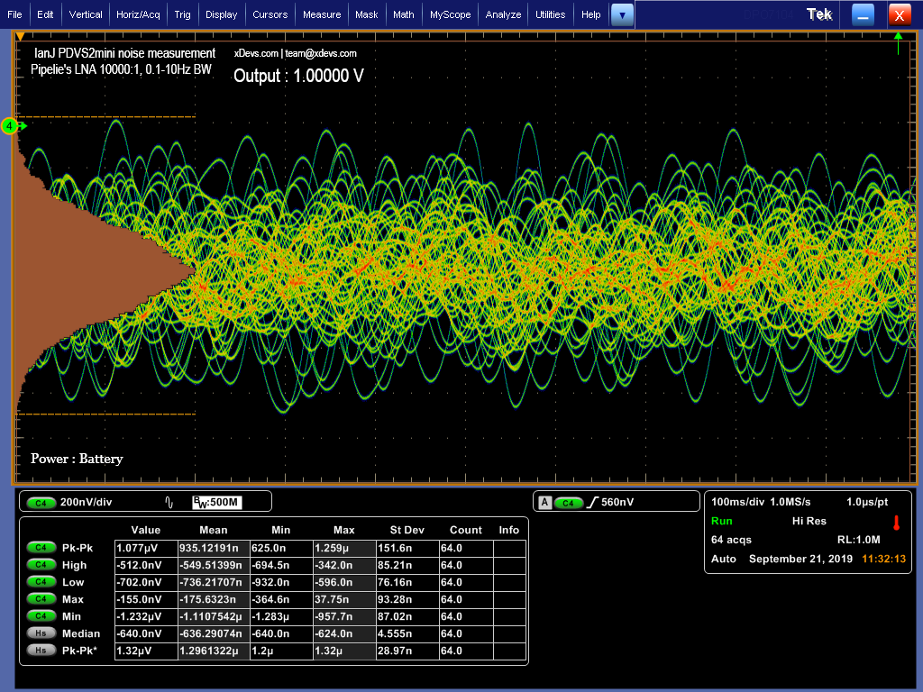
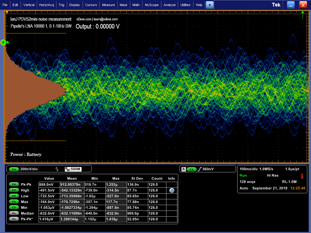
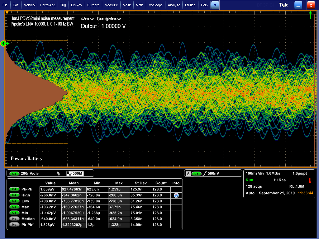
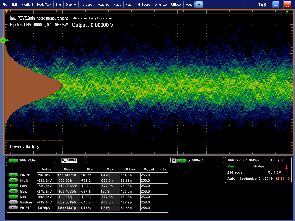
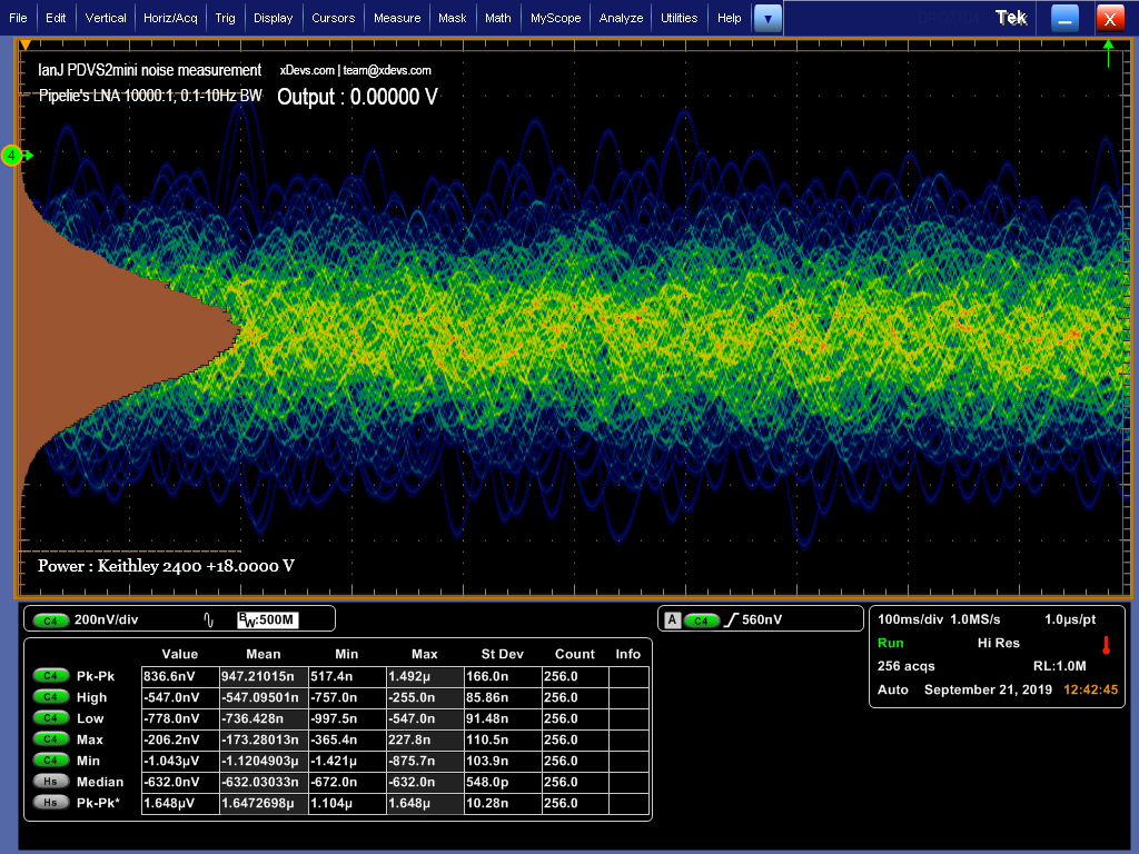
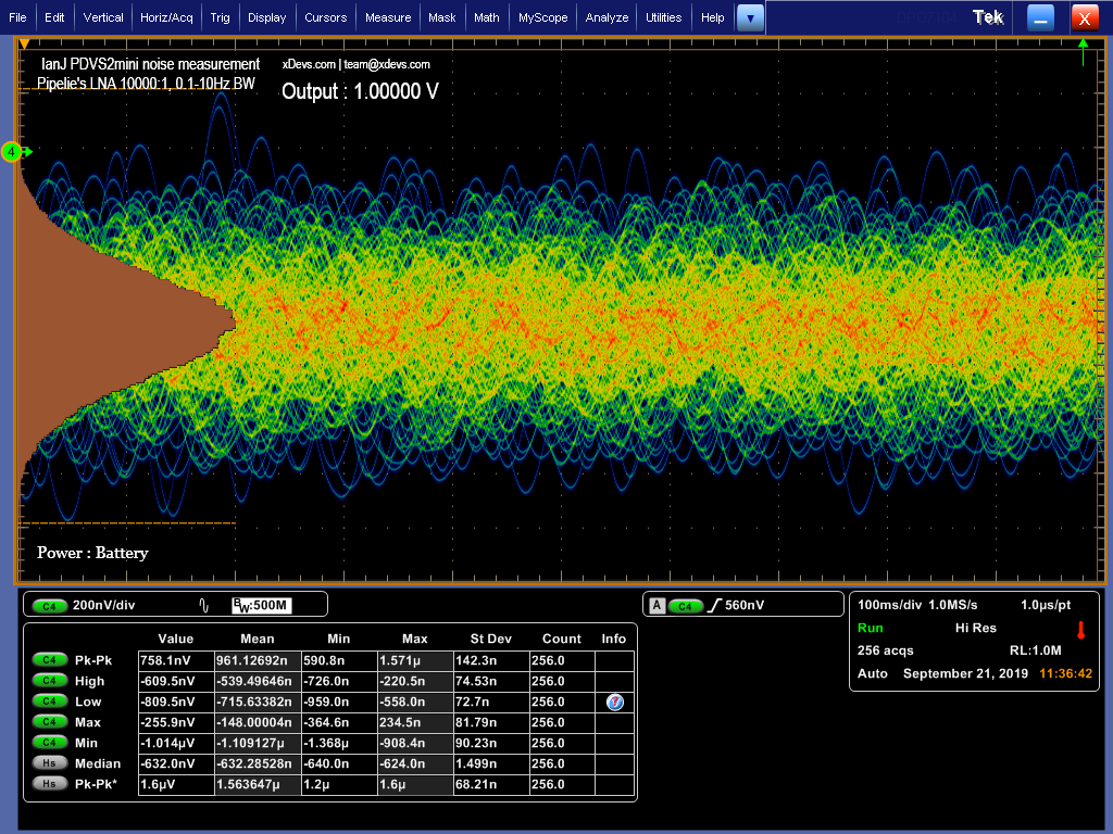
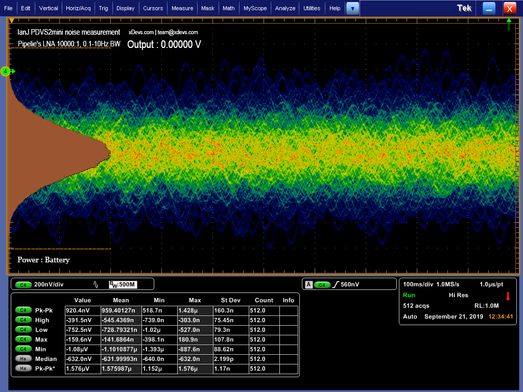
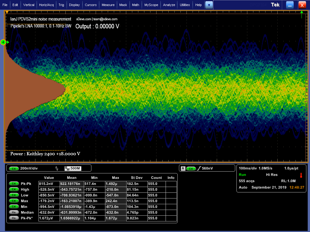
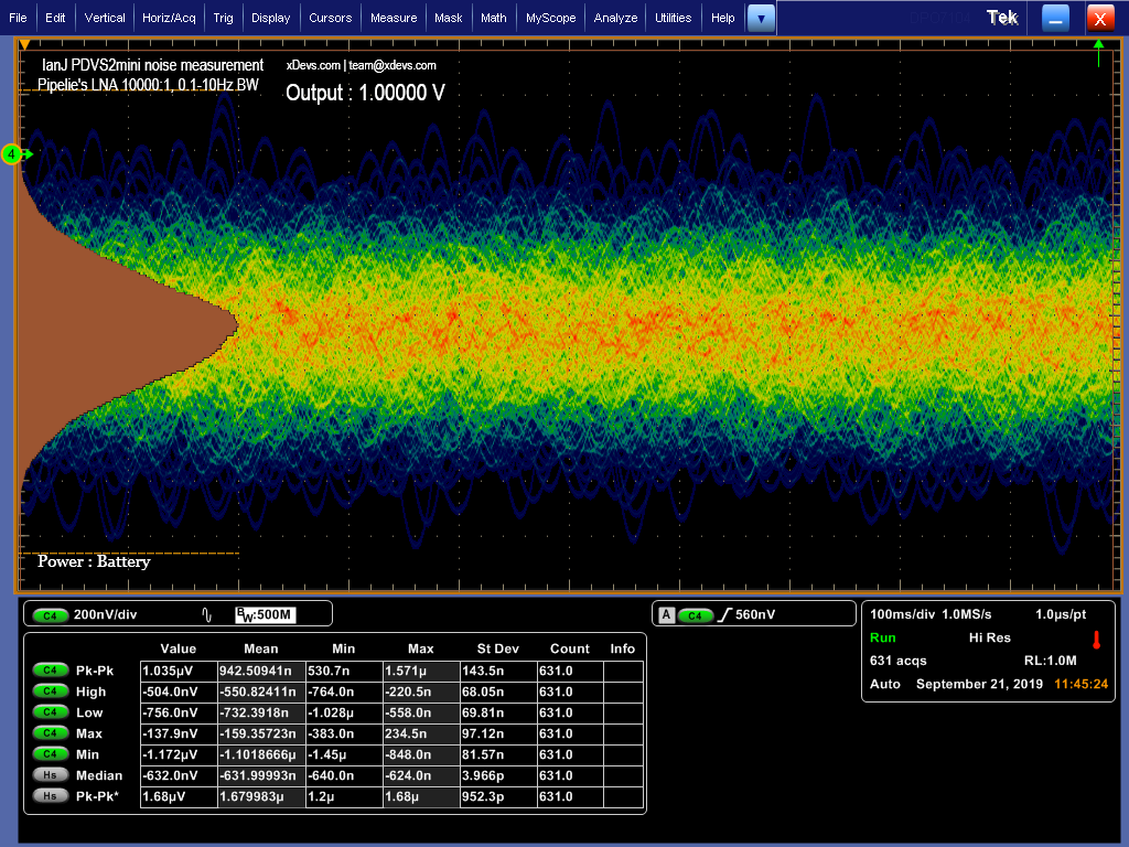
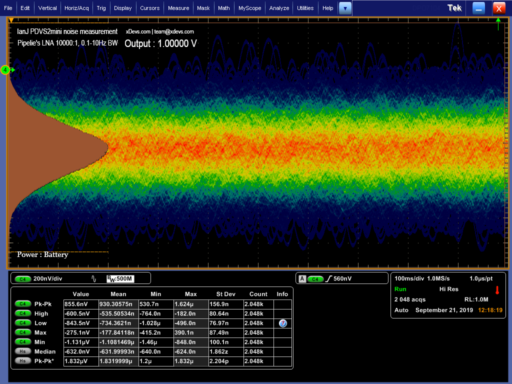
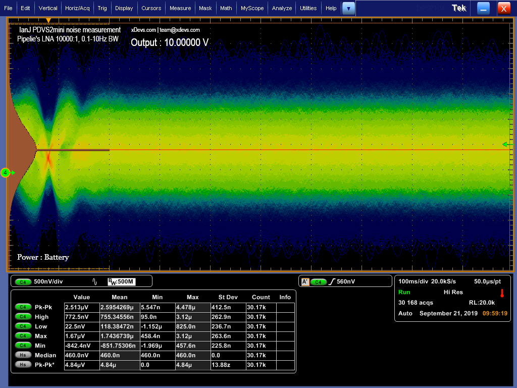
Two setup condition were used for PDVS2mini evaluation. Low noise floor is important when generating precise low voltages, such as reference values for thermocouple calibrations and sensitive amplifier circuit design. Essentially noise will be a limiting factor of this device performance in short-term like hours. Both setups used to measure same noise parameter, but with different bandwidth coverage.
Measurements with oscilloscope and LNA
For low-frequency and DC work many of components and circuits provided with noise performance over 0.1 – 10 Hz bandwidth. Voltage references and high-performance DACs (over 16 bits) often have low noise levels, and typical oscilloscope, even high-performance modern ones are not sensitive enough for such job. Best in class modern scopes might have 500 µV/division vertical scale and 14-bit ADCs but even that will only show own scope’s noise, and not the DUT.
To help with such noise measurement external high gain low-noise amplifier (LNA) is used. And because we want to measure only noise component, DC component of the output signal, such as +10.00000 VDC must be removed before the amplification can happen. This is done by using low-leakage AC coupling capacitor in the LNA front-end. And bandwidth limiting is also done by LNA itself, to reject any unwanted out of band signals.
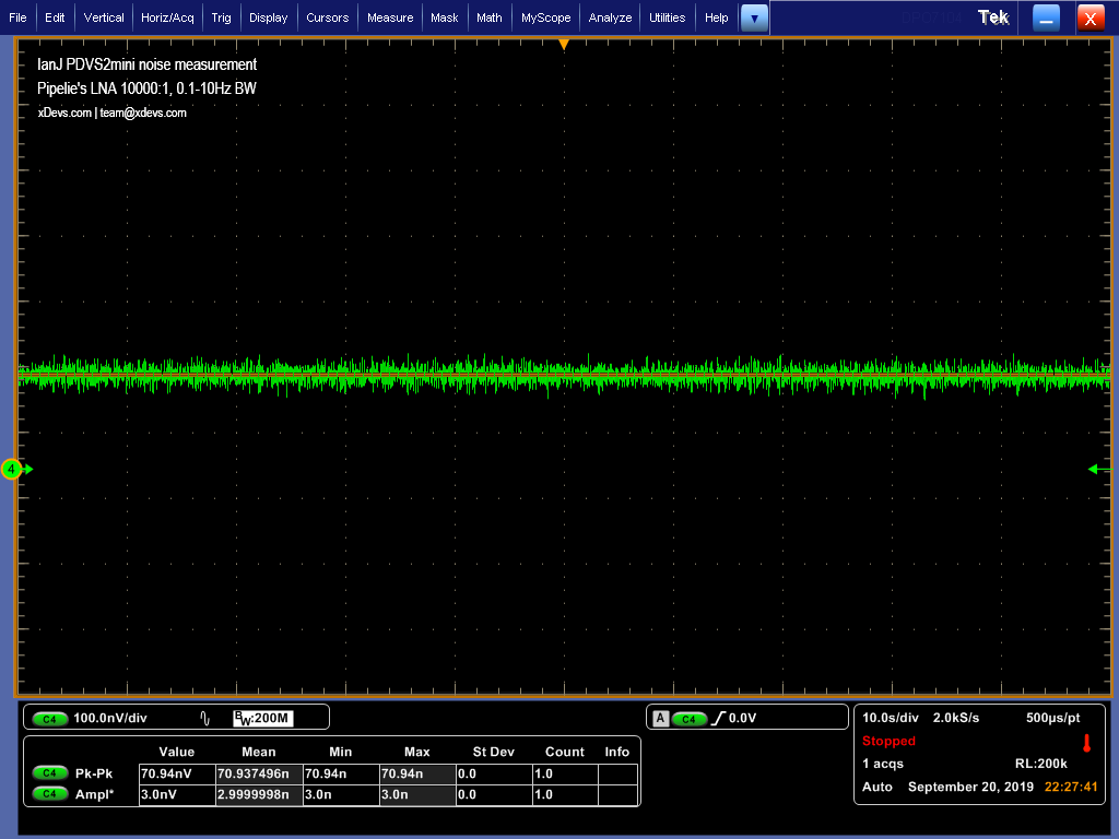
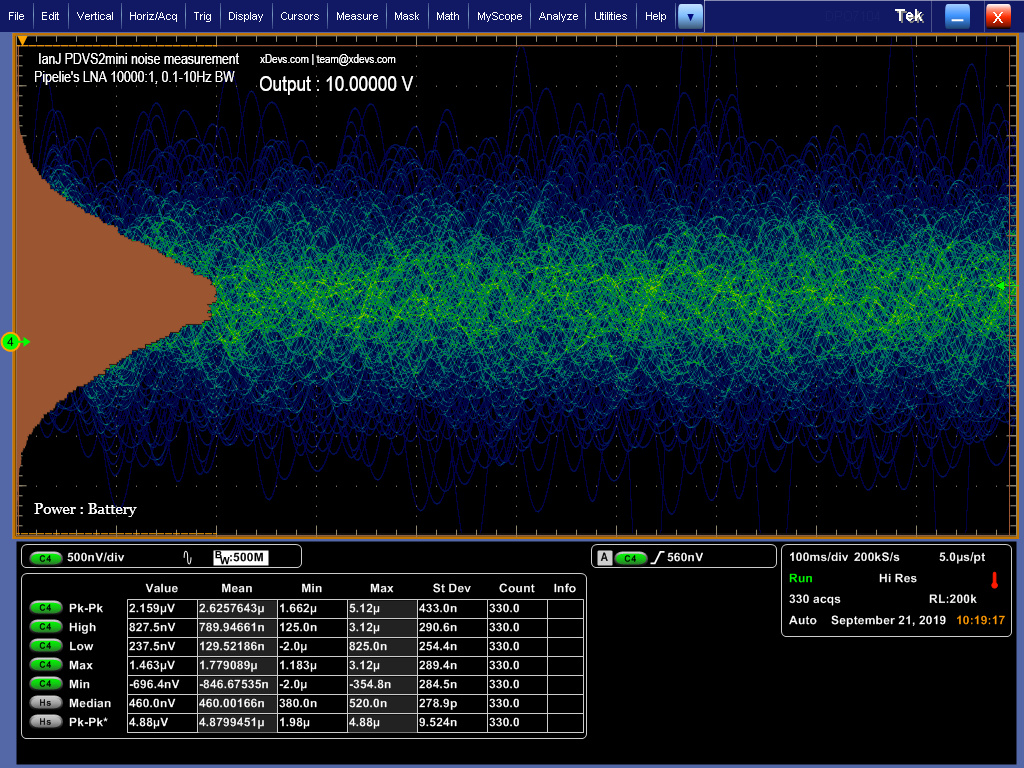
Our particular LNA is based on open lymex design, refined and manufactured by metrology enthusiast pipelie. LNA provide gain 10000, meaning that each 1 µV of AC signal at the input will translate into 10 mV at the output. In RF terms, amplifier has 60 dB of gain with 0.1 – 10 Hz bandwidth. Noise floor of setup with LNA’s shorted input reads around 71 nVpk-pk which is significantly lower than we expect to see from LM399A-based device under test.
Scope configured with the input impedance 1 MΩ. High-resolution mode was enabled to further reduce own scope bandwidth so it affects measurement much less. Setup was undisturbed, because any kind of vibration would be translated into noise due to microphonic and triboelectric effects in cables and boards. AC coupling input capacitor must be pre-charged to test DC voltage before the actual AC noise measurements can happen. This was taking sometimes over 15 minutes, depends on test conditions.
Waveforms are captured and processed by Tektronix DPO7104 digital oscilloscope. This scope has minimum vertical sensitivity 1 mV/div, which together with LNA translates into 100 nV/division. Connection between scope and Ian’s PDVS2mini was done with low noise short BNC-BNC coax cables to maintain complete shielding over the signal path. Transition from coax to dual 4mm banana jacks happens directly at the PDVS2mini output via regular Pomona BNC to dual banana adapter.
Set of multiple captures was stored, covering typical cardinal points of the PDVS2 mini, such as zero output, 10% and 100%. Example capture screenshot shown below.
Tests were performed with use of onboard battery power and external power from SMU, such as Keithley 2400. Summary of results provided in Table 2. SMU was configured to source +18.0000 VDC with current compliance set at 1.0000 A. All result data points have screenshots, clickable on each table point. All plots captured as multiple sweeps with 100ms/div horizontal resolution.
| PDVS2mini | 0V Battery | 0V SMU | 1V Battery | 10V Battery | 10V SMU |
|---|---|---|---|---|---|
| 8 runs, 1.25 Hz | 1.16 µVpk-pk, σ 3.7 nV | 1.25 µVpk-pk, σ 51 nV | 1.26 µVpk-pk, σ 27.5 nV | ||
| 16 runs, 0.625 Hz | 1.17 µVpk-pk, σ 6.5 nV | 1.42 µVpk-pk, σ 85.6 nV | 1.28 µVpk-pk, σ 33.3 nV | 3.96 µVpk-pk, σ 600 nV | |
| 32 runs, 0.3125 Hz | 1.32 µVpk-pk, σ 48.6 nV | 1.44 µVpk-pk, σ 93.3 nV | 1.30 µVpk-pk, σ 33.0 nV | 3.78 µVpk-pk, σ 780 nV | |
| 64 runs, 0.1563 Hz | 1.37 µVpk-pk, σ 93.9 nV | 1.60 µVpk-pk, σ 116.3 nV | 1.32 µVpk-pk, σ 30.0 nV | ||
| 128 runs, 0.0781 Hz | 1.42 µVpk-pk, σ 52.1 nV | 1.65 µVpk-pk, σ 66.0 nV | 1.33 µVpk-pk, σ 15.0 nV | 3.84 µVpk-pk, σ 144 nV | |
| 256 runs, 0.0391 Hz | 1.58 µVpk-pk, σ 51.8 nV | 1.65 µVpk-pk, σ 10.3 nV | 1.60 µVpk-pk, σ 68.2 nV | 3.84 µVpk-pk, σ 7.6 nV | |
| 512 runs, 0.0195 Hz | 1.58 µVpk-pk, σ 1.2 nV | 4.46 µVpk-pk, σ 184 nV | |||
| 555 runs, 0.0181 Hz | 1.58 µVpk-pk, σ 0.6 nV | 1.67 µVpk-pk, σ 9.0 nV | 1.68 µVpk-pk, σ 1 nV | 4.86 µVpk-pk, σ 202 nV | |
| 2048 runs, 0.005 Hz | 1.83 µVpk-pk, σ <1 nV | ||||
| 30168 runs, 0.0003 Hz | 4.84 µVpk-pk, σ <1 nV |
Projects like this are born from passion and a desire to share how things work. Education is the foundation of a healthy society - especially important in today's volatile world. xDevs began as a personal project notepad in Kherson, Ukraine back in 2008 and has grown with support of passionate readers just like you. There are no (and never will be) any ads, sponsors or shareholders behind xDevs.com, just a commitment to inspire and help learning. If you are in a position to help others like us, please consider supporting xDevs.com’s home-country Ukraine in its defense of freedom to speak, freedom to live in peace and freedom to choose their way. You can use official site to support Ukraine – United24 or Help99. Every cent counts.
Modified: June 19, 2024, 6:39 a.m.