Intro
Often there is a need to provide electrically quiet DC power to various analog circuits. Low noise applications, voltage references, precision ADC/DAC designs and sensor front-ends suffer from noisy power rails and often require use of inefficient linear power regulators. Typical switch-mode power supply is not suitable for such designs due to excessive high-frequency content present in the power output, EMI/RFI issues and shielding challenges.
It is possible to design of low noise DC-DC suitable to replace linear power regulators or in some cases even battery power, but it is no easy feat. We will try to look into this in this work.
Motivation for this project
New projects and ideas for voltage and resistance metrology require clean and efficient power supply with number of rails for various circuits and design blocks. Ideally whole supply should be able to accept 24V or 12V bulk input supply and efficiently generate multiple output rails, both with isolation and low noise. Next goals are selected as a target:
- +20…+36, +24 nominal VDC input from bulk AC\DC or battery pack
- Very low noise on output rails, ideally below 150 µVpp under full load
- +15V DC output rail 1A
- -15V DC output rail 1A
- +5V DC output rail 2A
- +3.3V DC output rail 2A
- Efficiency better than 60% on loads from 20 to 80%
- Status signals (over-current, over-voltage, overheat outputs)
- Switching cycle synchronization with external clock
- Shielded assembly to reduce RFI
- 4-layer low cost PCBA
- BOM cost under $500 USD per unit
Concept
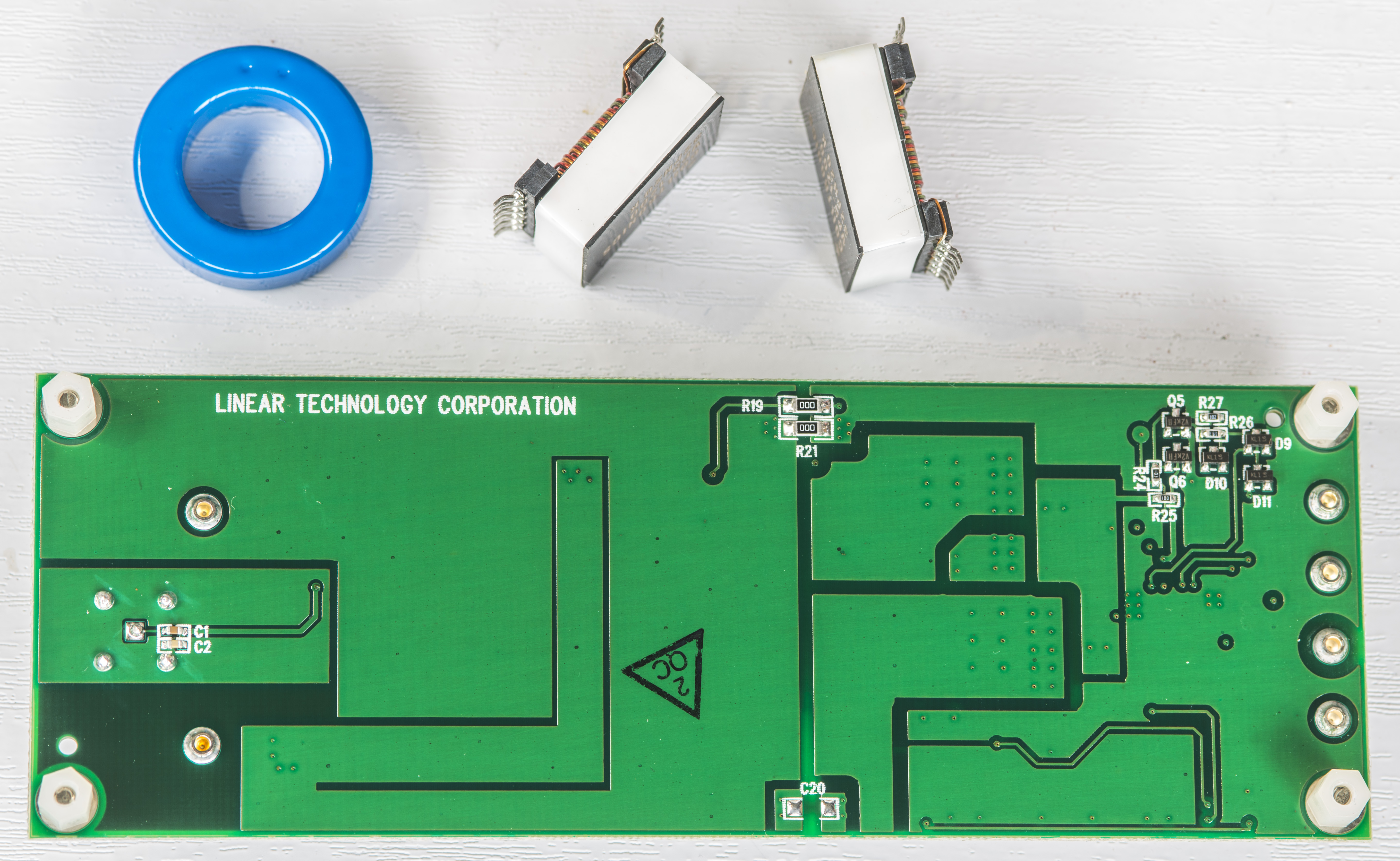
LTC DC477A is a development board for LT1683 controlled slew-rate switch-mode power converter. It is specially suited for cases where low noise and low EMI/RFI qualities are first importance. Linear (now ADI) LT1683 is special IC for medium power converter designs, while LT1533 is more integrated solution with internal power stage. Both chips are offering low noise operation which is achieved by providing user control of the output switch slew rates. Voltage and current slew rates can be independently programmed to optimize switcher harmonic content versus efficiency. Before doing own custom design PCBA one approach is to start testing various component and topology choices using DC477 evaluation platform.
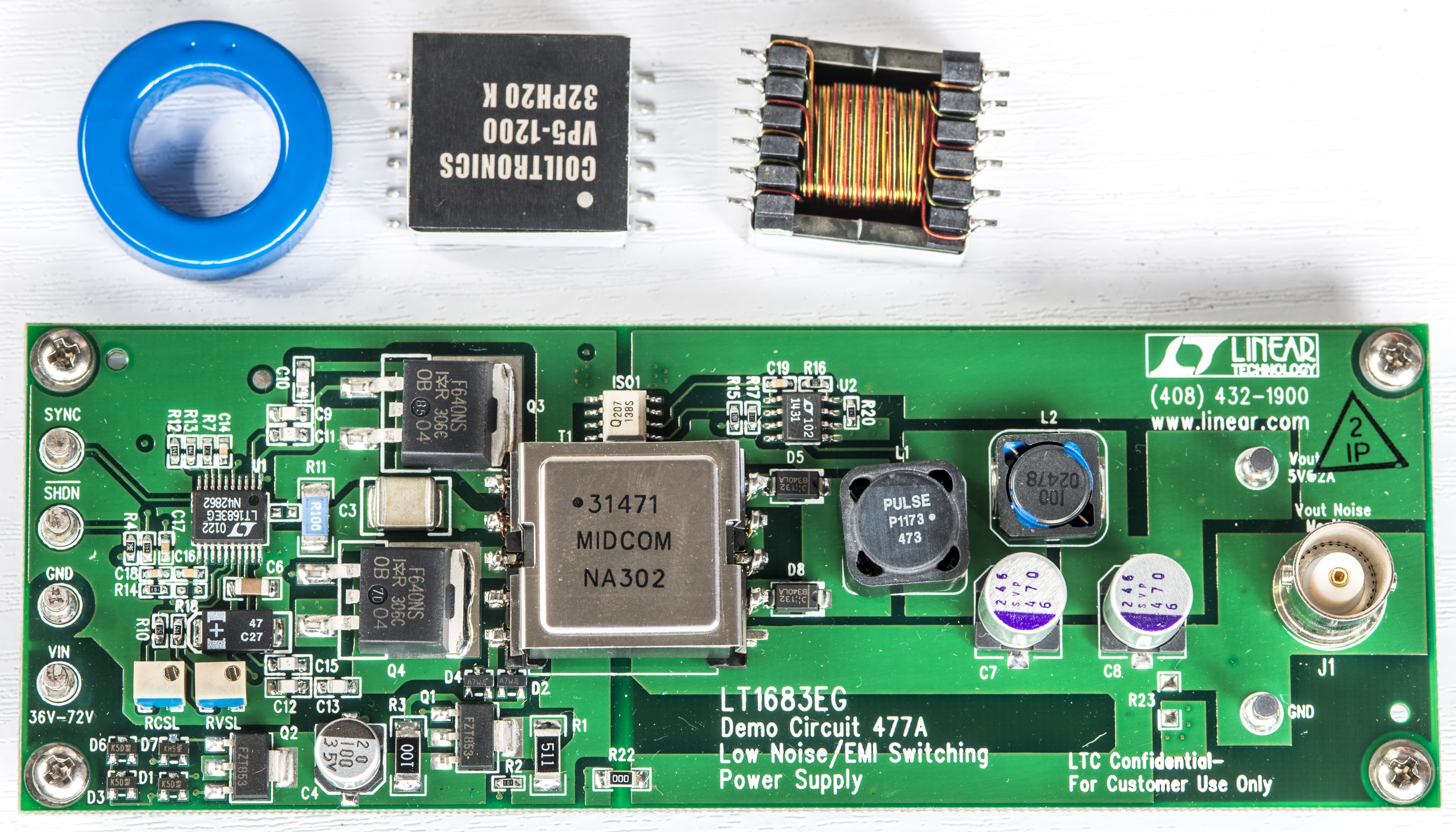
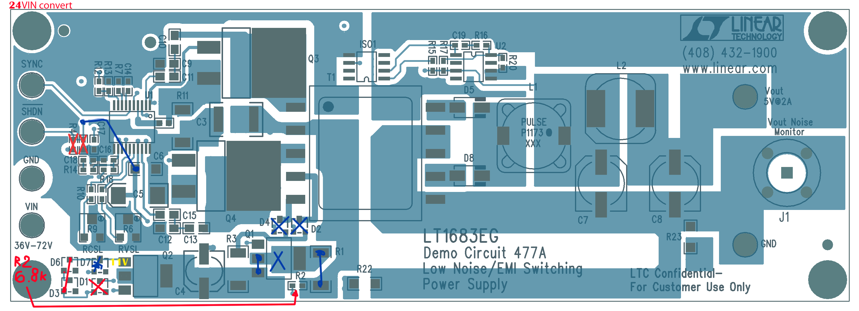
Original development board configuration fitted to run from +36-72 VDC power input. My application have bulk DC rail available only at lower +24V DC voltage, so minor reworks and modifications are required to enable operation of the converter module with reduced input power.
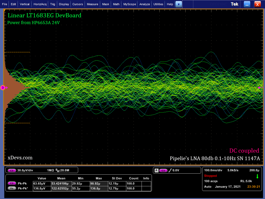
After modifications I’ve powered board from HP 6653A linear DC power supply and performed noise measurements with 80dB 0.1-10 Hz preamplifier and Tektronix DPO7104C oscilloscope. AC coupling capacitors on the bottom side of DC477A near BNC connectors were shorted to allow measurement of low frequency noise in 0.1-10 Hz bandwidth.
Keithley 2425 SMU was used as programmable DC load. Module is configured as non-isolated +5V output supply.
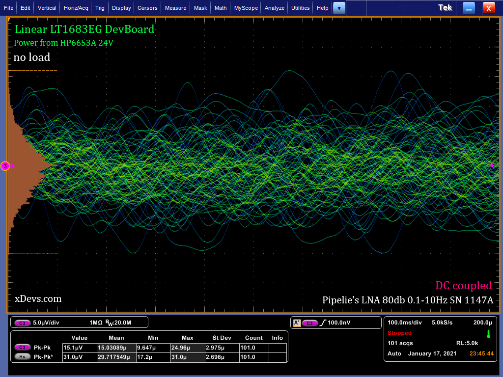
First test is without any load connected at the output. Noise measured at 31 µVpeak-peak. Please note 5 µV/div vertical scale.
Second test is with 1000 mA applied as load connected at the output. Noise measured at 136 µVpeak-peak. Please note 30 µV/div vertical scale.
Efficiency of the power conversion measured at 75.7% (24.008 VIN, 0.235 AIN, 4.271 VOUT, 1.000 AOUT).
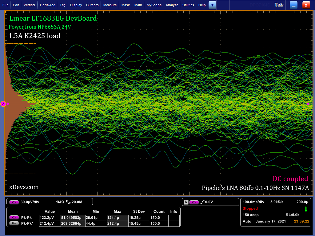
Third test is with 1500 mA applied as load connected at the output. Noise measured at 212 µVpeak-peak. Vertical scale is same with 1.0A test.
TBC
Projects like this are born from passion and a desire to share how things work. Education is the foundation of a healthy society - especially important in today's volatile world. xDevs began as a personal project notepad in Kherson, Ukraine back in 2008 and has grown with support of passionate readers just like you. There are no (and never will be) any ads, sponsors or shareholders behind xDevs.com, just a commitment to inspire and help learning. If you are in a position to help others like us, please consider supporting xDevs.com’s home-country Ukraine in its defense of freedom to speak, freedom to live in peace and freedom to choose their way. You can use official site to support Ukraine – United24 or Help99. Every cent counts.
Modified: June 19, 2024, 6:46 a.m.