Intro
Ten years is a lot of time for digital electronics technology, and ALTERA Stratix FPGA line evolved to 6th generation in 2016, featuring very fast on-die HBM2 memory and 56Gbps XCVRs on Stratix 10 MX devices. New technology such as Intel EMIB, Intel 14 nm Tri-Gate process and many more made all this possible.
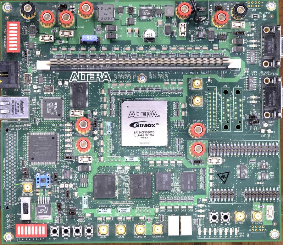
Let’s take a look where we started back in 2002 with first generation 130nm Stratix and how it still can help makers and digital design engineers. Sometime ago I got myself an ALTERA development kit targeted for memory interfacing and design, using EP1S40 device.
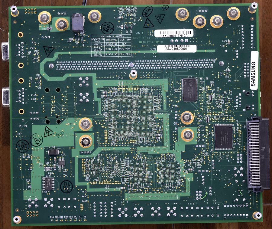
This board main purpose to debug and evaluate various memory interfaces using legacy Stratix FPGA. Take a look on block diagram:
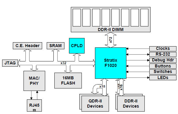
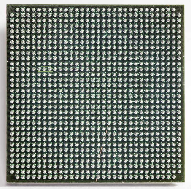
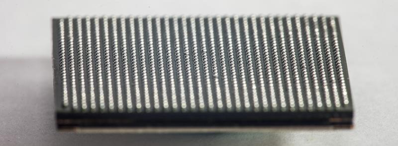
Used EP1S40F1020C5 device is fastest speedgrade medium-size chip in the family, using FineLine 1020-ball BGA package.
- 80 transmit and 80 receive source synchronous channels
- 41250 LEs, 3423744 RAM bits (417KB)
- 12 PLLs (8 Fast and 4 Enhanced)
- 10 transmit and 10 receive medium speed channels
- 112 DSP block 9-bit elements
- 781 user I/O
- SMA interfaces for external I/O
There is also additional ALTERA MAX CPLD (EPM7256AETC144) for JTAG configuration and managment of FPGA.
SMB2 Board have various memory types available to developer:
- 2 x Micron Technology DDR2 SDRAM, 16M x 16 Memory Devices (MT47H16FG-5E), 200MHz
- 2 x Cypress Semiconductor QDR2 SRAM, 1M x 18 Memory Devices (CY7C1313V18-200BZC), 200MHz
- 1 x DDR2 SDRAM DIMM Module, 32M x 72, Memory Device (such as Micron MT9HTF3272-40E), 200MHz
- 1 x Flash 128Mbit Memory Device (AMD AM29LV128MH113REI)
- 2 x SRAM 256K x 16 Memory Devices (IDT71V416S10PH)
Documentation
ALTERA Stratix™ Memory Board 2, Datasheet. April 2004, Ver.0.3
ALTERA Stratix™ Memory Board II Rev A, User Guide, June 2004, Ver.0.2
Like with many development kits, there are also full schematic available in PDF and OrCAD DSN formats and layout source files.
Cadence PCB design v15.0 board layout file
Cadence PCB design v16.3 board layout file
Board BOM in MS Excel XLS format
Complete ALTERA kit documentation package, including all files above, ZIP 18.5 MB
Unfortunately, this board does not function as expected, and FPGA chip does not detect in USB-Blaster JTAG chain, nor getting configuration via ISP interface. Initial inspection and measurements did not reveal anything wrong, all power rails were good, JTAG TDI,TMS,TCK lines have correct signals, but TDO output pin on Stratix does not give anything. Pushing and flexing PCB in hope of bad BGA contact did not help either.
ALTERA’s documentation for this family logic devices will be handy too:
ALTERA Stratix Handbook, Volume 1 and Volume 2
Repair
Buying new high-end FPGA from retailer can be costly lesson. You may think, it’s 12 years old, surely it’s not that expensive? Well, DigiKey have pricing for EP1S40F1020C5 for $2618 USD each, if you able buy lot of 24 pieces. Not a viable option for fixing old development board for some educational use, I’d say.
Stratix FPGAs even on secondary market are still expensive devices, alternative risky path was chosen for this repair. Sometimes there are broken/damaged boards are being sold for little money, where such FPGAs may be installed. If we assume FPGA chip as good, have tools and skill to remove large BGA package, re-ball it and solder back on our PCB, then it could all work out. So to try this I bought broken Infinera TAM40G test board for $50 USD.
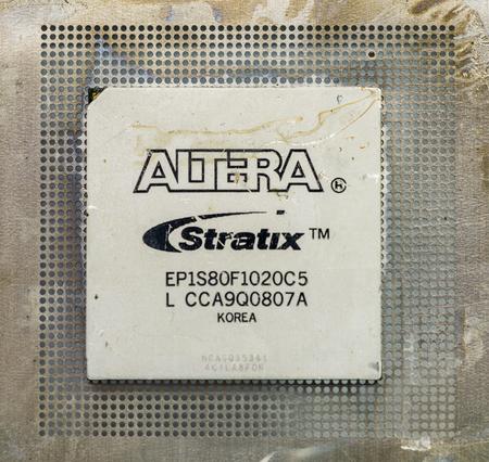
This board have pair of EP1S80F1020C5 FPGAs in same package, and since these are compatible devices (1S80 have double of the logic elements and few more transievers, but same pinout) we have two chances to try this. Infinera specialize at communication and networking backbone equipment, and little known about this TAM40G board. Large 10-layer board have lots of useful components though, so let’s look thru features on it first.
Board overview
I already desoldered one of Stratix FPGA’s off the board before taking photo, sorry about that. Even though Stratix 1S80 is old chip, it’s even higher $11459 USD price for a piece on Digikey may faint some novice engineers. This IC is top of the family line, providing 79040 logic elements, 7427520 bits of RAM bits and 22 DSP blocks.
There are also pair of ALTERA Cyclone II EP2C50 used onboard is $240 chip and EP1C12 is $50.
Fixed delay line ELMEC
Analog Devices ADM1069 supervisor – 9$
TI DAC7821 12-bit MDAC 20.4MSPS 2.6$
AD9765 – 12bit 125MSPS Dual TxDAC+ $15
Silabs Si5326 ultra-low jitter 2kHz-945MHz clock multiplier $57
Microchip SY89540U cross-switch LVDS 11$
1 x TI DAC5662AI Dual, 12-Bit, 275 MSPS Digital-to-Analog Converter
2 x Linear LTC1645 Dual-Channel Hot Swap Controller/Power Sequencer.
2 x Linear LTM4600EV 10A High Efficiency DC/DC µModule 4.5-20Vin
Linear LT4222 Dual Hot Swap Controller with I2C Compatible Monitoring
2 x ALTERA EP1S80F1020C5
2 x ALTERA EP1C12F324C8
2 x ALTERA EP2C50F484C7
2 x ALTERA MAX II EPM240GT100C3N 1.8Vcore
2 x ALTERA EPC16UC88 16Mbit Configuration Device
3 x Marvell 88×2040 Alaska X 10 Gigabit XAUI to XGMII Transceiver
1 x TI TLK10021 10Gbps XAUI-XFI Phy for XFP module
2 x Broadcom BCM8152CIFB – 10Gbps XFP Transceiver
4 x TI CDCP1803 1:3 LVPECL Clock Buffer with Programable Divider
4 x TI PTH04000WAS 3A DC-DC modules
Bunch of TI TPS761xx LDOs
Micrel SY58611U 2.5GHz LVDS 2:1 ultra-low jitter mux
Input power hot-plug
J1 -> pair of IRF6635 FETs
10-layer stackup:
After providing board with +3.3V and +5V from PC PSU and poking around with USB ByteBlaster I got EP2C50 detected:

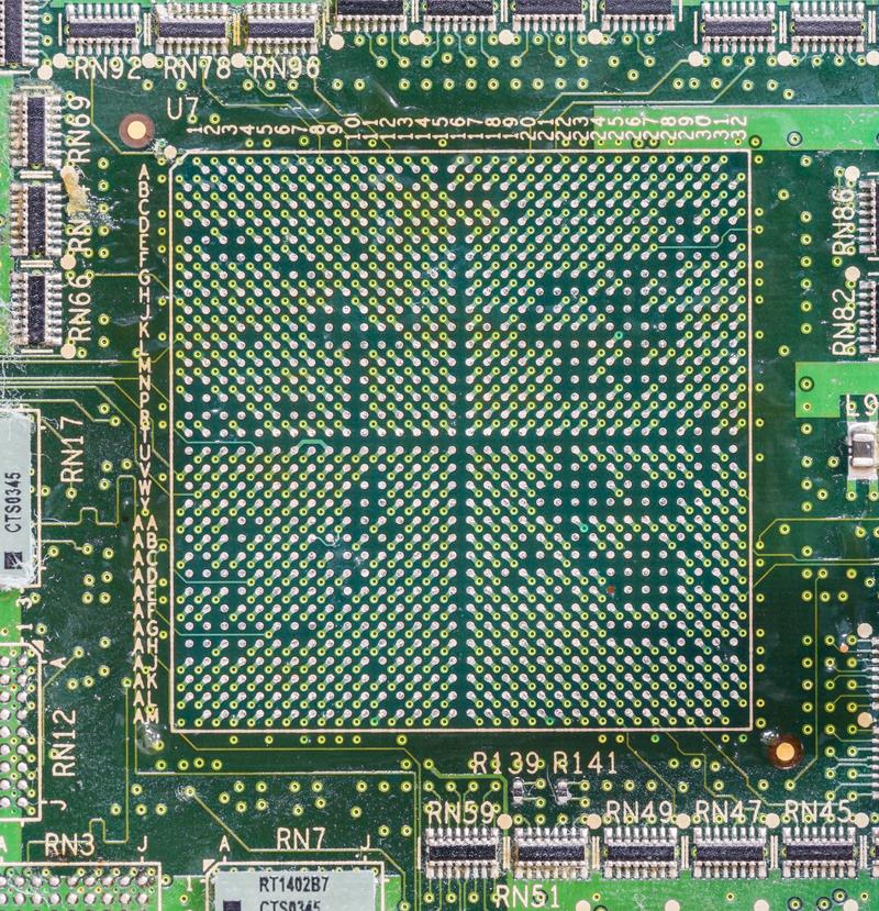
Replacing FPGA chip on PCBA
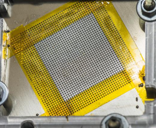
To replace BGA chip few steps are required:
1. Remove board from donor board
2. Reball removed chip (restore uniform ball grid)
3. Make sure all balls are in place and leveled.
4. Add flux paste specified for BGA rework on PCB and align FPGA chip on pads straight.
For this task few extra items:
- Stencil. I bought univeral set of these stencils from eBay
- BGA flux
- 0.6mm Pb-free balls
- Kapton tape to secure FPGA chip in place with stencil
3. Mount reballed chip on target PCBA
Bonus shots
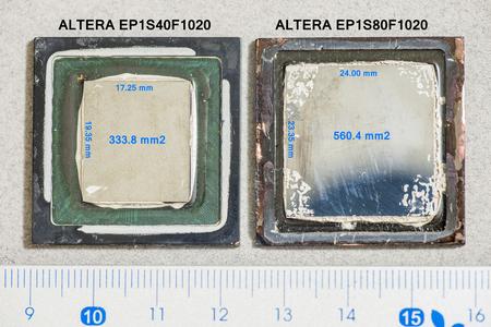
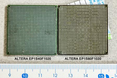
I also had removed copper heatspreader top of BGA package of old Stratix devices and measured die size.
Obviously, these are two different devices with different dies. Larger FPGA is over 70% larger in silicon area, hence large price increase. It’s always very expensive to make large chips, no matter which node process used, 130nm or today’s best 14nm.
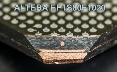
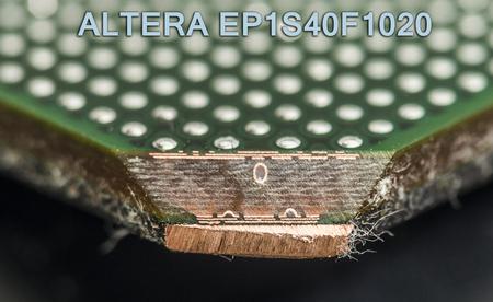
Also as both FPGAs are non-functional bit of more teardown was performed, by cutting corner of package to reveal copper layers:
That’s it for now, let us know your feedback.
Projects like this are born from passion and a desire to share how things work. Education is the foundation of a healthy society - especially important in today's volatile world. xDevs began as a personal project notepad in Kherson, Ukraine back in 2008 and has grown with support of passionate readers just like you. There are no (and never will be) any ads, sponsors or shareholders behind xDevs.com, just a commitment to inspire and help learning. If you are in a position to help others like us, please consider supporting xDevs.com’s home-country Ukraine in its defense of freedom to speak, freedom to live in peace and freedom to choose their way. You can use official site to support Ukraine – United24 or Help99. Every cent counts.
Modified: July 21, 2016, 3:18 p.m.

