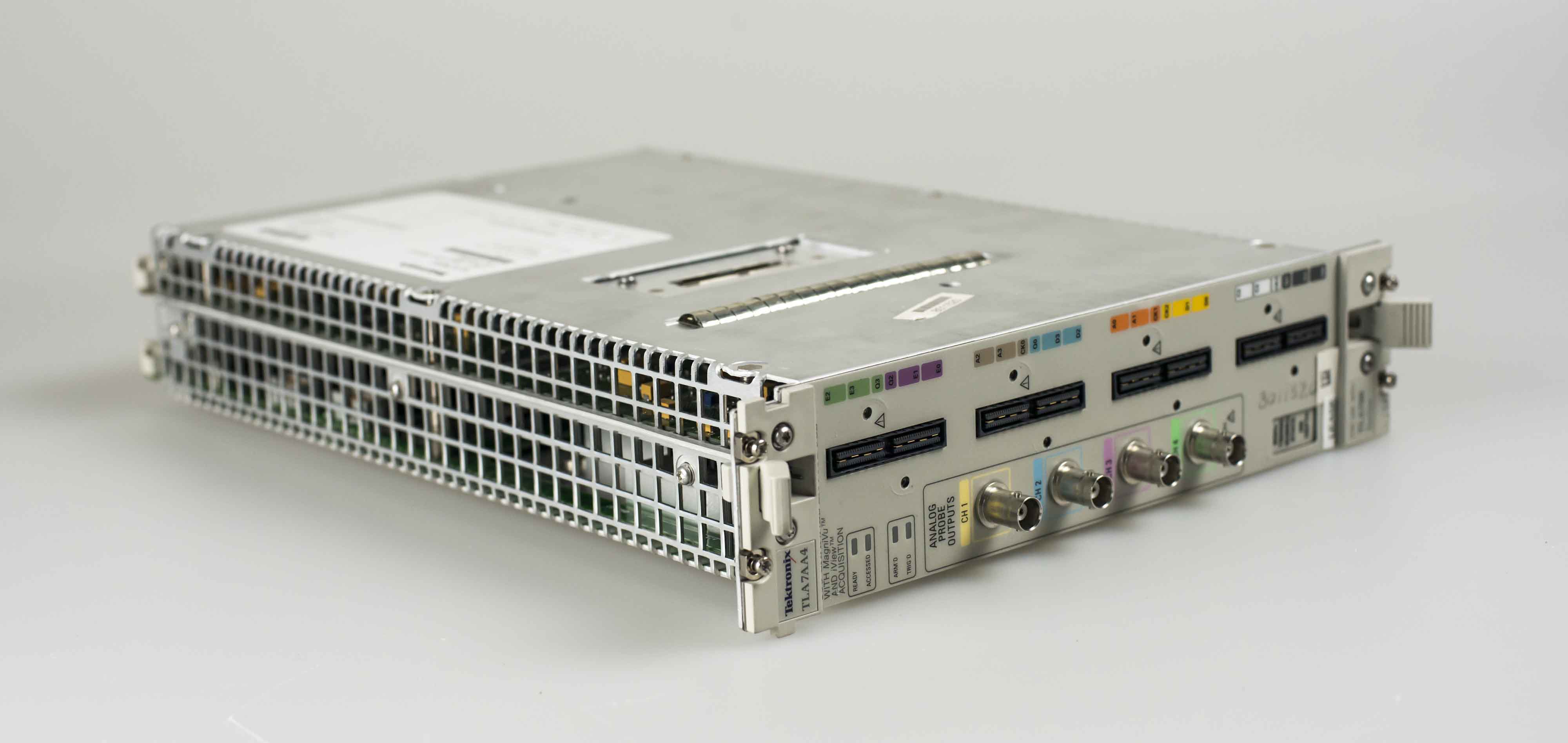
Module exterior
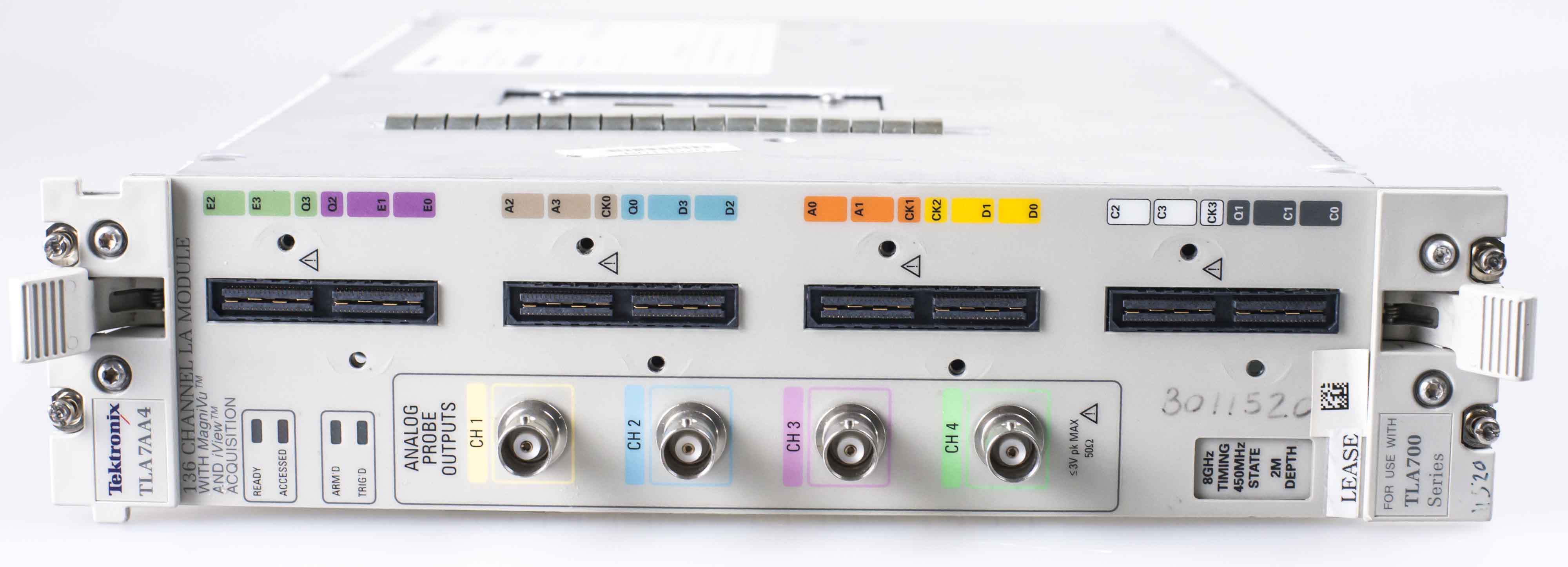
Front panel (the only area available to user when module is installed in logic analyzer mainframe) have four input channel ports, each having 34 channels. There are four LED indicators to display current condition of module (Ready, Accessed, ARM’d, TRIG’d). Our TLA7AA4 was in CS option configuration, which allows 8GHz Timing speed and 450 MHz state speed, with 2M depth of memory.
There are other modules in series such as:
- TLA7AA1 – 34 channels, 2 are clock channels, 4 demultiplexed BNC outputs for iView™ Analog Outputs (10x attenuation, 2GHz typical bandwidth)
- TLA7AA2 – 68 channels, 4 are clock channels, 4 demultiplexed BNC outputs for iView™ Analog Outputs (10x attenuation, 2GHz typical bandwidth)
- TLA7AA3 – 102 channels, 4 are clock channels and 2 qualifier channels, 4 demultiplexed BNC outputs for iView™ Analog Outputs (10x attenuation, 2GHz typical bandwidth)
- TLA7AA4 – 136 channels, 4 are clock channels and 4 qualifier channels, 4 demultiplexed BNC outputs for iView™ Analog Outputs (10x attenuation, 2GHz typical bandwidth)
- TLA7NA1 – 34 channels, 2 are clock channels
- TLA7NA2 – 68 channels, 4 are clock channels
- TLA7NA3 – 102 channels, 4 are clock channels and 2 qualifier channels
- TLA7NA4 – 136 channels, 4 are clock channels and 4 qualifier channels
Module chassis is made of aluminum and heavily perforated from sides to allow air flow thru mainframe.
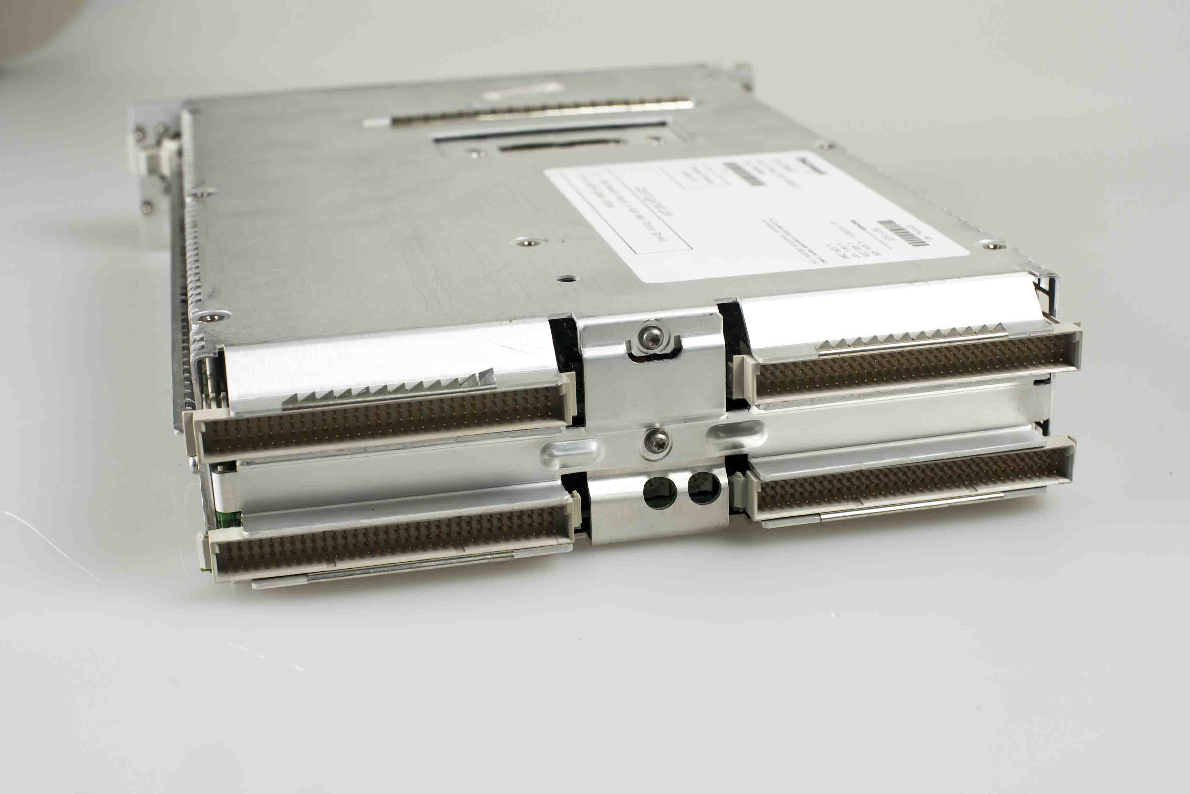
Back connector is coupling to TLA’s VXI bus via four connectors. VXI address is set via rotary switches on backside of module as well.
Module side have merge connector, which allow to combine multiple modules together for united triggering and channel grouping.
Currently six different types of active probes are supported for the logic analyzer TLA7AA/TLA7NA/TLA7AB modules:
- P6810 34-channel general purpose probe
- P6860 34-channel high-density single-ended probe
- P6864 17-channel high-density 4X single-ended probe
- P6880 34-channel high-density differential probe
- P6960 34-channel high-density single-ended probe with D-Max probing technology
- P6980 34-channel high-density differential probe with D-Max probing technology
Compression type probe heads, such as P6860 do not require PCB connector, and mate directly to pads on PCB. Probe is fixed by pair of 2-56 nuts on opposite board side. This is great way to save on debug connectors and avoid BOM increase due to debug requirements.
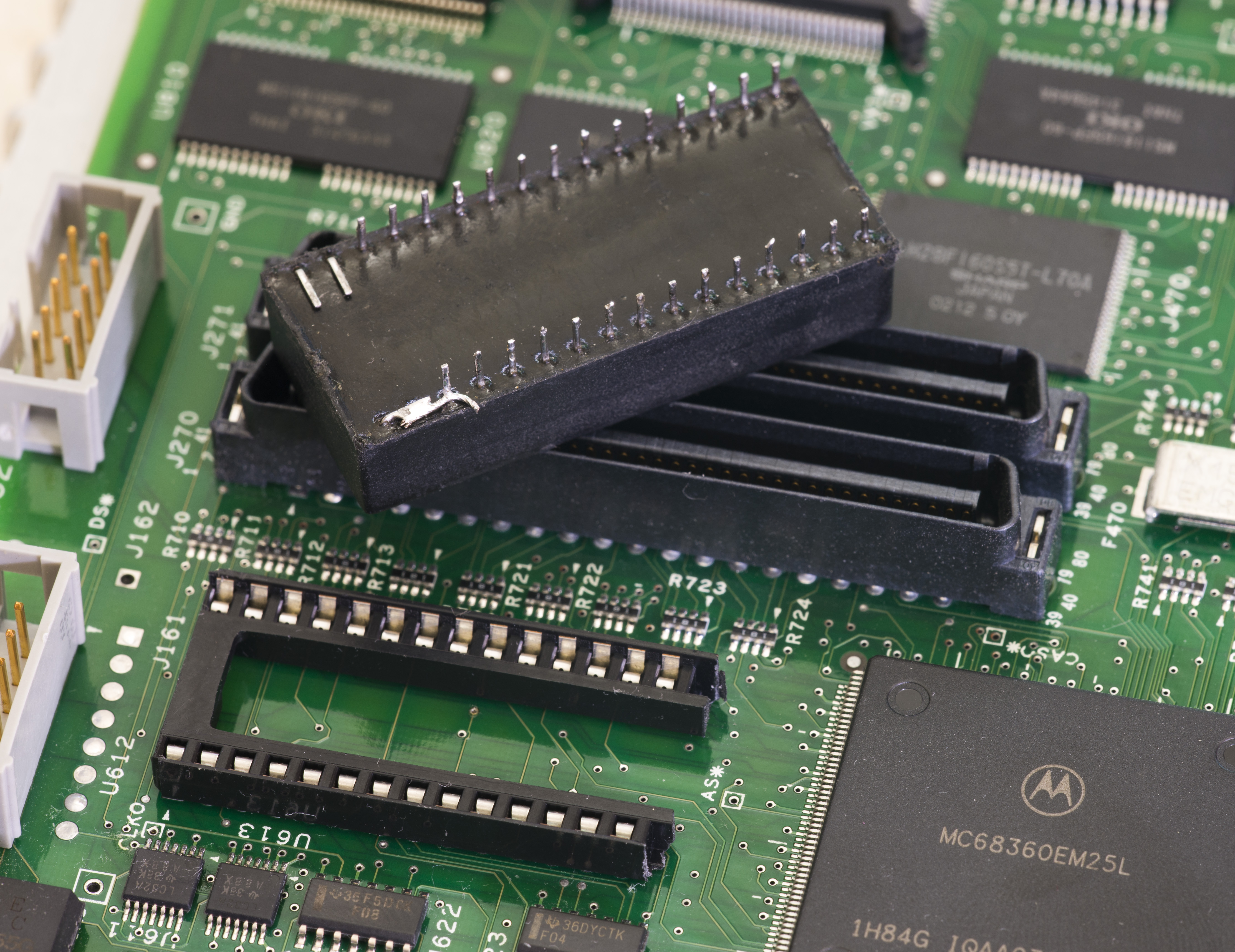
Module interior
Acquisition board
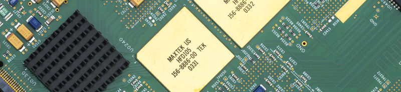
7AA4 have two main PCBs, similar separated architecture to 7000 series oscilloscope, with acquisition board to handle all raw data processing, storage and triggering and digital PowerPC board running VxWorks

Both side photos captured in 64 Megapixels and are available in very high resolution for your enjoyment. Main acquisition board is 14-layer beast with lots of unobbtanium Tektronix ASICs and lots of memory.
Golden MAXTEC HFD105 ASICs in center are likely handling multiplexing logic analyzer channels for analog BNC outputs.
Mezzanine input port connectors soldered directly to PCB edge, in close proximity to front end ASICs, providing well characterized matched length signal path. On speed of hundreds of megahertz everything in physical layout and location become very important, so it’s vital to keep all parts with minimal distances.
The probe interface consists of ASICs that receive data from the probes, compare the data against a threshold, and transfer the digital information to CMOS ASICs via differential outputs. Each ASIC in the probe interface receives 16 data channels and one clock channel.
Triggering
Clocking and triggering is controlled by a single ASIC U450. This ASIC determines when acquisition data should be sampled based on the clock information and qualifier information. The ASIC also contains 16 Event resources for the purposes of word recognition, range recognition, and other trigger functions. In merged configuration, the ASIC communicates information between modules to ensure proper triggering.
Few lonely Xilinx Spartan XC2S50 in FBGA256 packages likely doing glue logic to digital computer PCB, which sits on top of acquisition board.
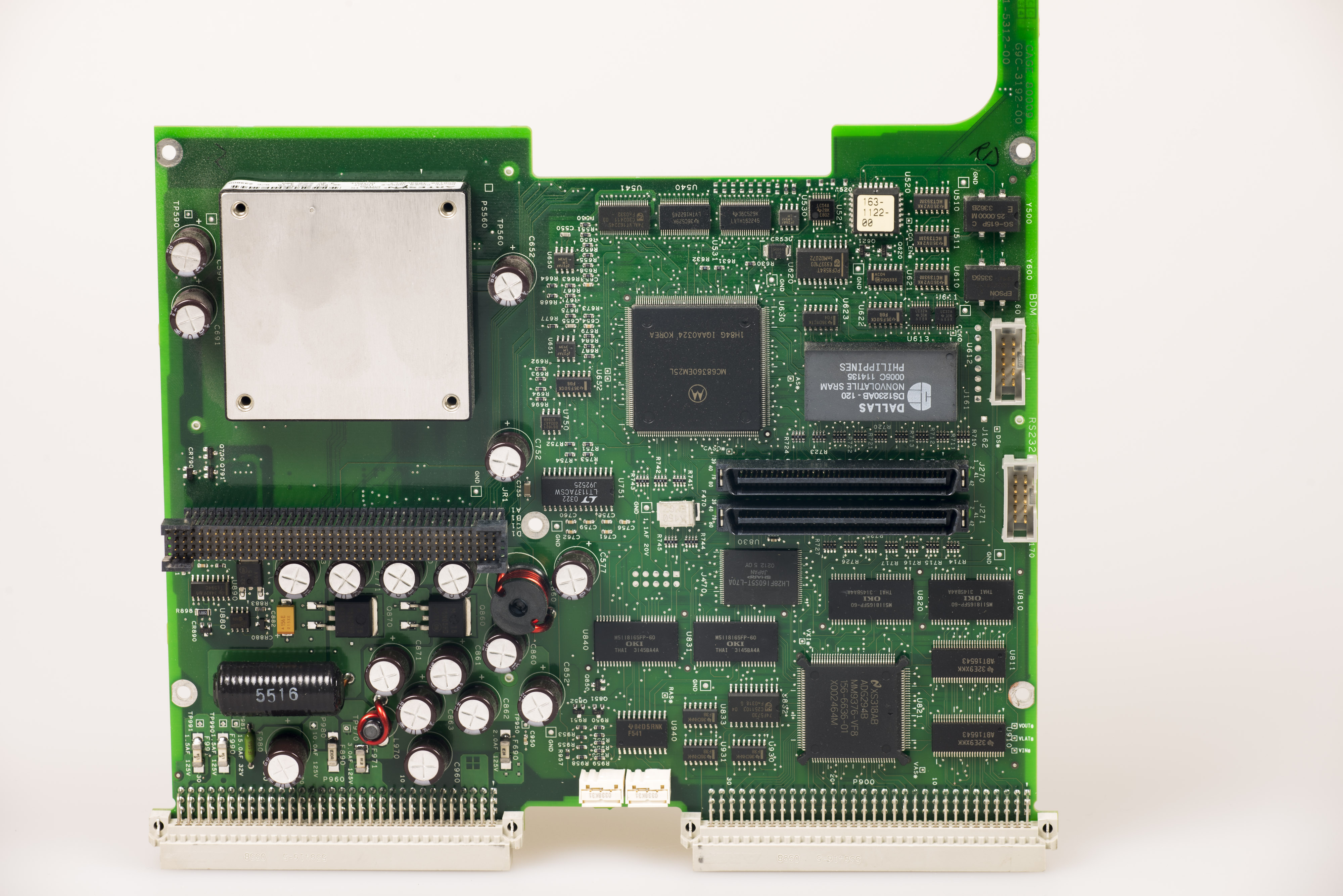
Local Processor Unit board
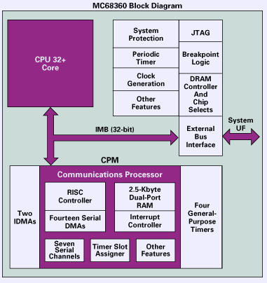
Local Processor Unit board using Motorola MC68360EM25L. According to Freescale’s documentation it is 32-bit controller that is an extension of other members of the Motorola M68300 family. The QUICC is comprised of three modules: the CPU32+ core, the SIM60, and the CPM. Each module utilizes the 32-bit IMB. The MC68360 QUICC block diagram is shown below
Other components around on digital module are:
- Sharp LH28F160S5T-L70A 16MBit NOR Flash memory, for storing OS and firmware
- Few banks of OKI MSM511816SFP-60 SRAM 16MBit memory, 60ns speedgrade
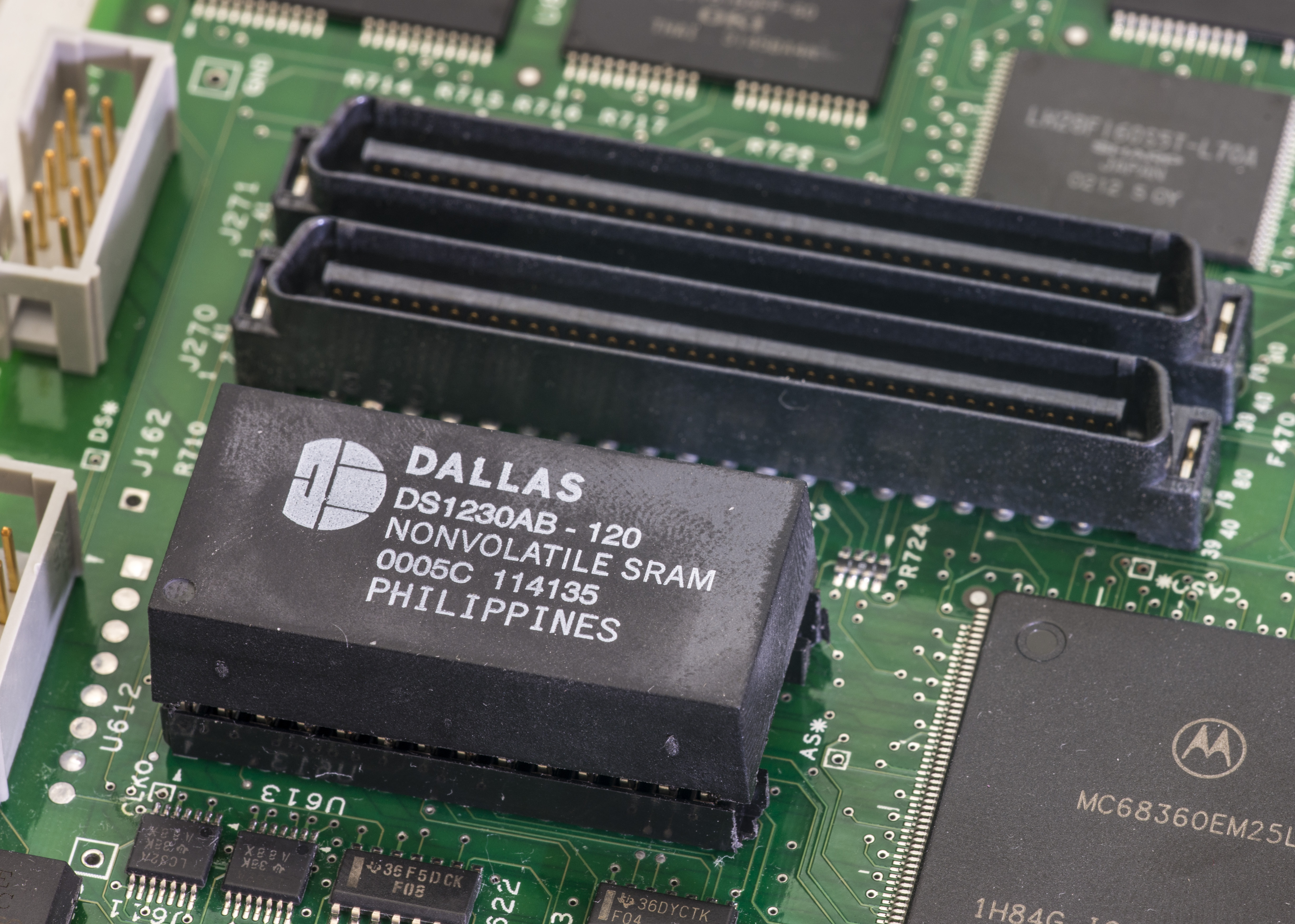
- DALLAS DS1230AB NVRAM chip in EDIP package (soldered onboard directly)
- Linear LT1137ACSW TTL-RS232 convertor chip (similar purpose as popular MAX232), driving RS232 serial debug port
- National Semiconductor ADG294B VXI Interface ASIC, which taking address/data and talks to VME bus.
- NXP PCF8584T I2C to Parallel bus converter
- Some more digital logic and PAL
There is also high-quality Artesyn DC-DC power supply module. The onboard power supplies receive +5 V, —5.2 V, ±12 V, and ±24 V from the mainframe through the rear connectors.
Then voltage converters produce the +2.5 V supply for use on the acquisition board through the 160-pin connector between the LPU and acquisition board.

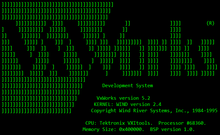
CPU is running Windriver VxWorks 5.2 real-time operation system. There is possibility to access terminal messages/debug via serial port:
Option settings
TLA7AA4 module using software keys to configure/lock their enabled memory amount and speeds. Hardware is well designed and capable for maximum capacity/speed, but can be often limited by software, to allow differentiation by price.
Here is reference table with possible options for TLA7AA1/TLA7AA2/TLA7AA3/TLA7AA4 modules:
| Option | Description |
| 1S | Increase to 512 Kb memory depth , 120 MHz state speed |
| 2S | Increase to 2 Mb memory depth , 120 MHz state speed |
| 3S | Increase to 8 Mb memory depth , 120 MHz state speed |
| 4S | Increase to 32 Mb memory depth , 120 MHz state speed |
| 5S | Increase to 128 Kb memory depth , 235 MHz state speed |
| 6S | Increase to 512 Kb memory depth , 235 MHz state speed |
| 7S | Increase to 2 Mb memory depth , 235 MHz state speed |
| 8S | Increase to 8 Mb memory depth , 235 MHz state speed |
| 9S | Increase to 32 Mb memory depth , 235 MHz state speed |
| AS | Increase to 128 Kb memory depth , 450 MHz state speed |
| BS | Increase to 512 Kb memory depth , 450 MHz state speed |
| CS | Increase to 2 Mb memory depth , 450 MHz state speed |
| DS | Increase to 8 Mb memory depth , 450 MHz state speed |
| ES | Increase to 32 Mb memory depth , 450 MHz state speed |
Same table for TLA7AB2 and TLA7AB4
| Option | Description |
| 1S | Increase to 64 Mb memory depth , 235 MHz state speed |
| 2S | Increase to 64 Mb memory depth , 450 MHz state speed |
And for TLA7NA1/TLA7NA2/TLA7NA3/TLA7NA4
| Option | Description |
| 7S | Increase to 2 Mb record length |
| 8S | Increase to 8 Mb record length |
| 9S | Increase to 32 Mb record length |
| 45 | Increase state speed to 450 MHz |
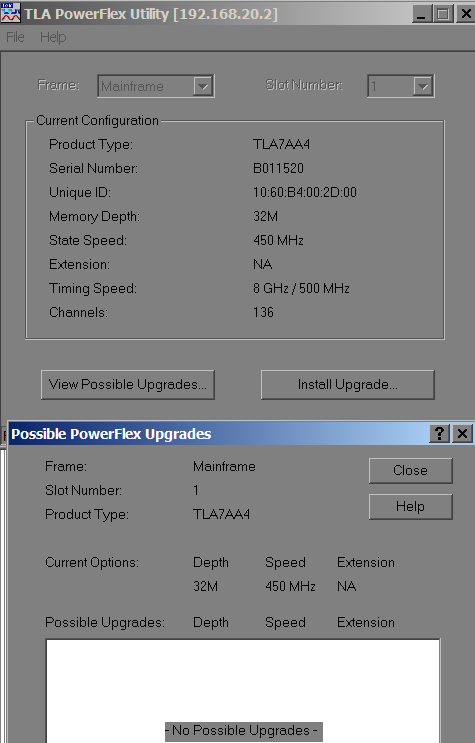
During initial investigation it was possible to “unlock” full speed/capacity by simple replacement of on-board DS1230AB to DS1245, likely due to firmware bug or NVRAM addressing issue.

To detect current enabled configuration/upgrade Tektronix supply PowerFlex utility, which come with TLA Application package.
Our TLA7AA4 stock configuration was Option CS
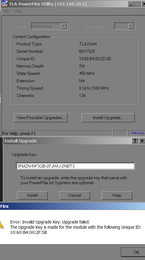
After replacement NVRAM to DS1245Y I’ve got this:
If you like this kind of review, or have any questions, feel free to discuss in comments.
Projects like this are born from passion and a desire to share how things work. Education is the foundation of a healthy society - especially important in today's volatile world. xDevs began as a personal project notepad in Kherson, Ukraine back in 2008 and has grown with support of passionate readers just like you. There are no (and never will be) any ads, sponsors or shareholders behind xDevs.com, just a commitment to inspire and help learning. If you are in a position to help others like us, please consider supporting xDevs.com’s home-country Ukraine in its defense of freedom to speak, freedom to live in peace and freedom to choose their way. You can use official site to support Ukraine – United24 or Help99. Every cent counts.
Modified: Feb. 8, 2016, 2:38 p.m.