The Teledyne LeCroy ZS1500 is a 1.5 GHz single-ended high-impedance active voltage probe with 10:1 attenuation.
As of 2020-10-17 it is an active product and retails for $2049 USD , however it is on the old side of LeCroy’s probe offerings and is likely to be phased out in the next few years.
It is listed as being compatible with the following instrument families:
- WaveSurfer 3000z
- WaveSurfer 4000HD
- WaveSurfer 510
- HDO4000A
- HDO6000A
- HDO8000A
- WaveRunner 8000
- WaveRunner 8000HD
- WaveRunner 9000
- MDA 8000HD
- MDA800A
- WavePro HD
- WaveMaster/SDA/DDA 8 Zi-B
LeCroy ZS1500 active probe manual
The ZS1500 appears to use the active probe head of the PMK Tetris 1500 but with a custom power module featuring a Teledyne LeCroy ProBus interface instead of the simple BNC + power connection on the stock Tetris probe. The ZS1500 also has internal offset control, a feature that the OEM version lacks.
The probe described in this review was purchased as manufacturer refurbished and predates Teledyne’s acquisition of LeCroy, and thus has the old logo on it.
Overview
The probe consists of a large extrusion with screw-on end caps containing the power supply and related components, connected via a multiconductor cable to the handpiece. The handpiece is quite small and comfortable to hold in the hand. While it gets perceptibly warm during use, it does not get unpleasantly hot to the touch even during extended test sessions. A bipod probe positioner is provided, which works well when using the longer ground leads but can be a bit tricky to use with the stiffer blade-style grounds.
There are no user facing adjustments on the probe, although two trimmers are present internally for use during calibration.
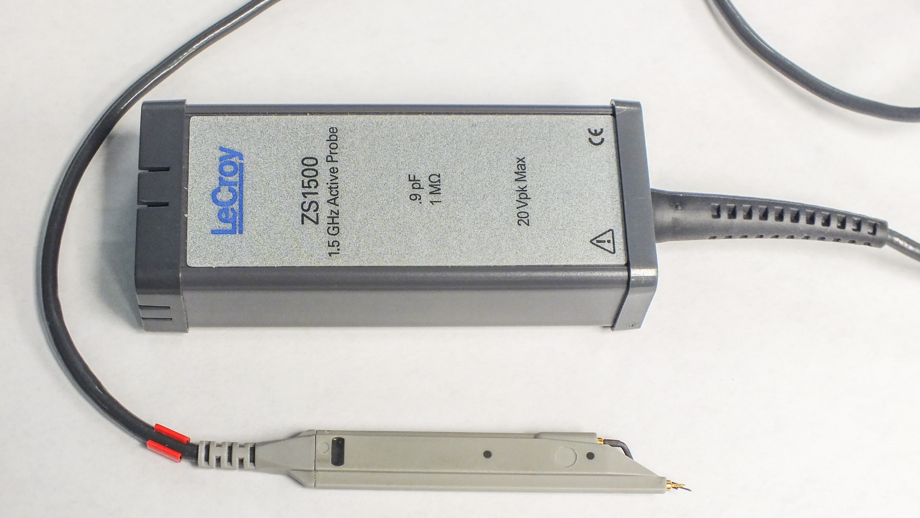
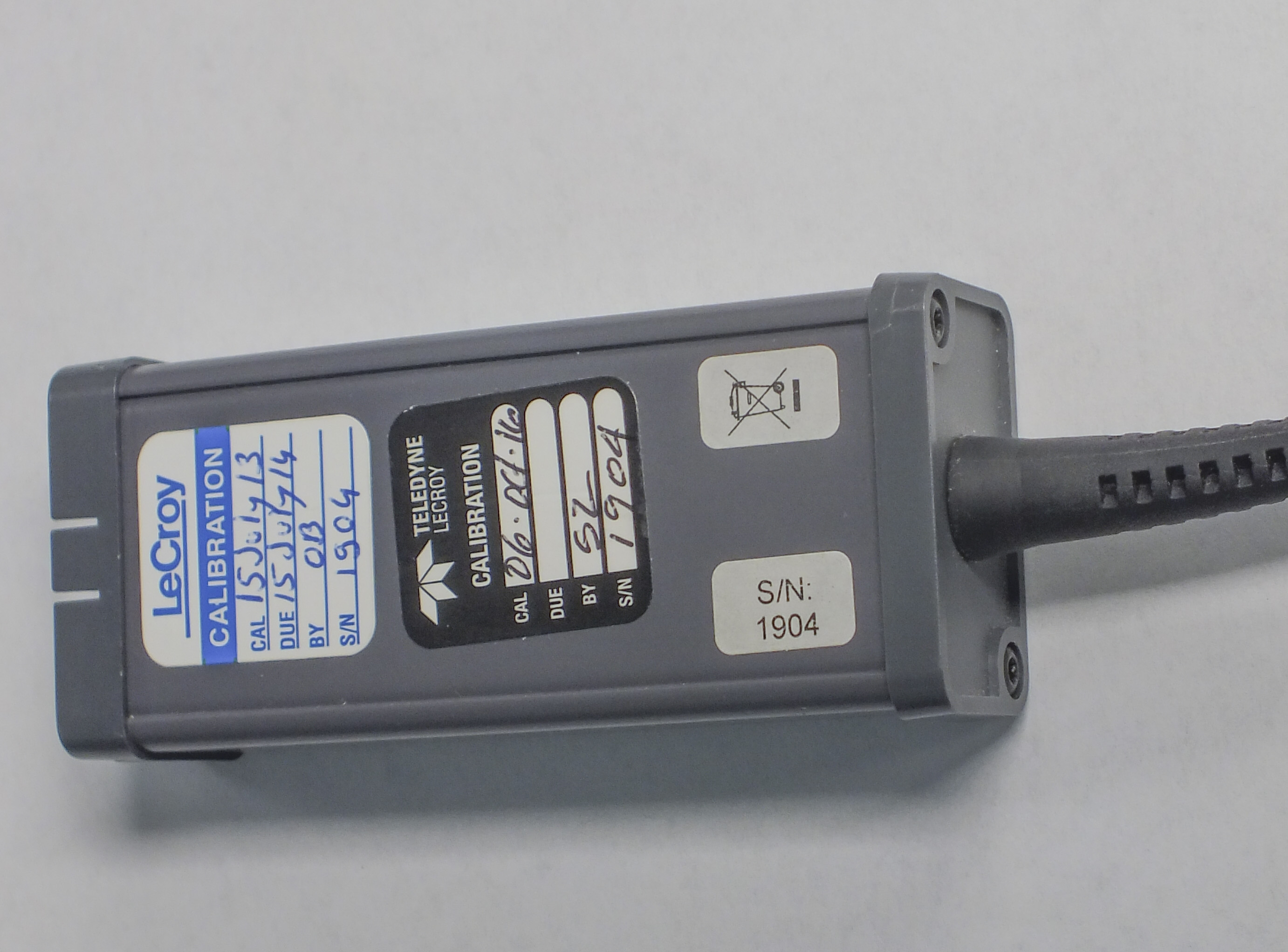
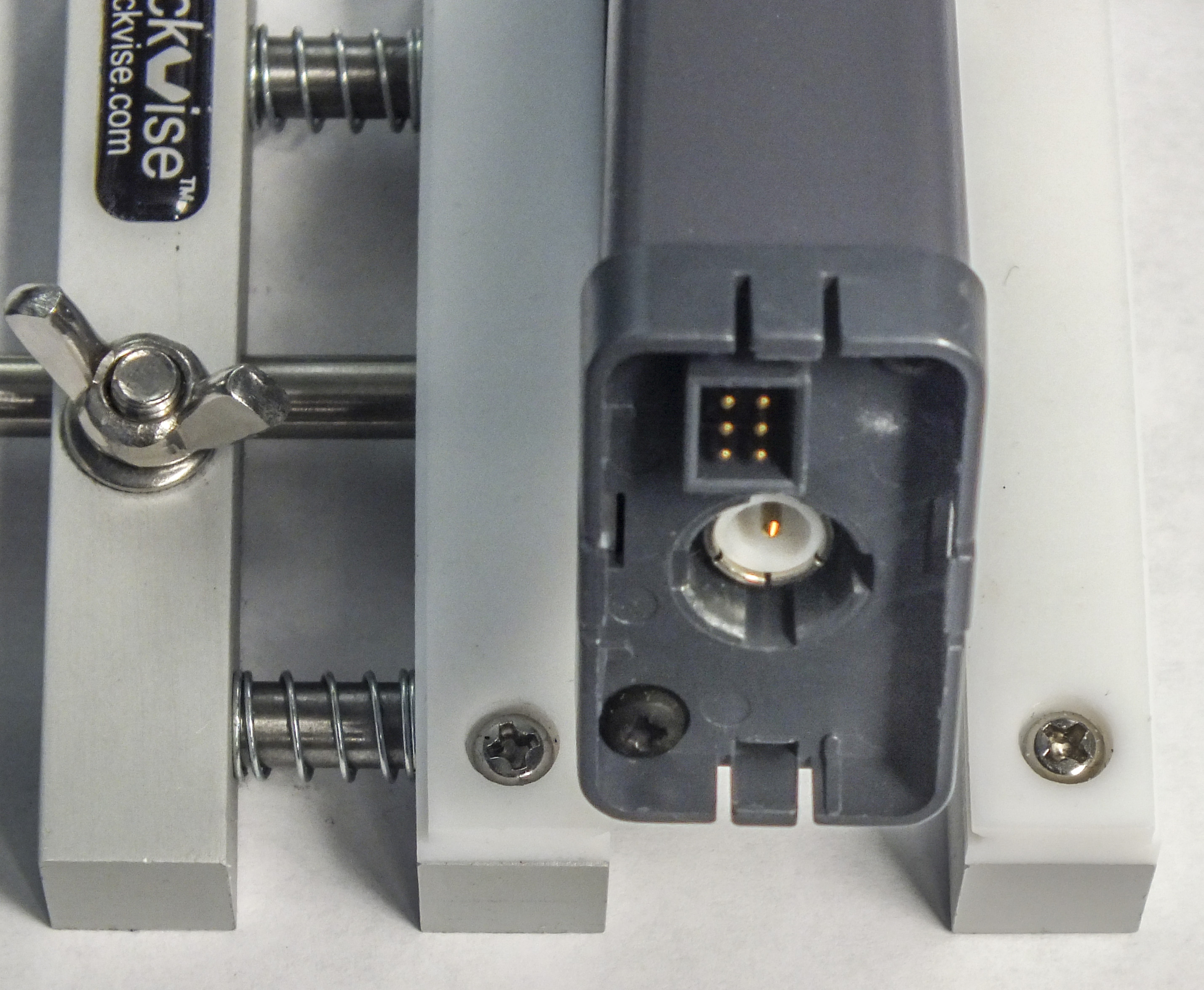
Image 1-3: Probe overview
Power Supply Module
The power supply module is a single U-shaped PCB which straddles the BNC signal connector. All interior surfaces of the enclosure are coated with some sort of conductive (nickel?) finish for EM shielding.
The cable from the power supply to the handpiece contains a coaxial RF cable surrounded by a secondary jacket which also contains three small cables, presumably providing various power voltages to the active amplifier module.

Image 4: Probe body PCBA
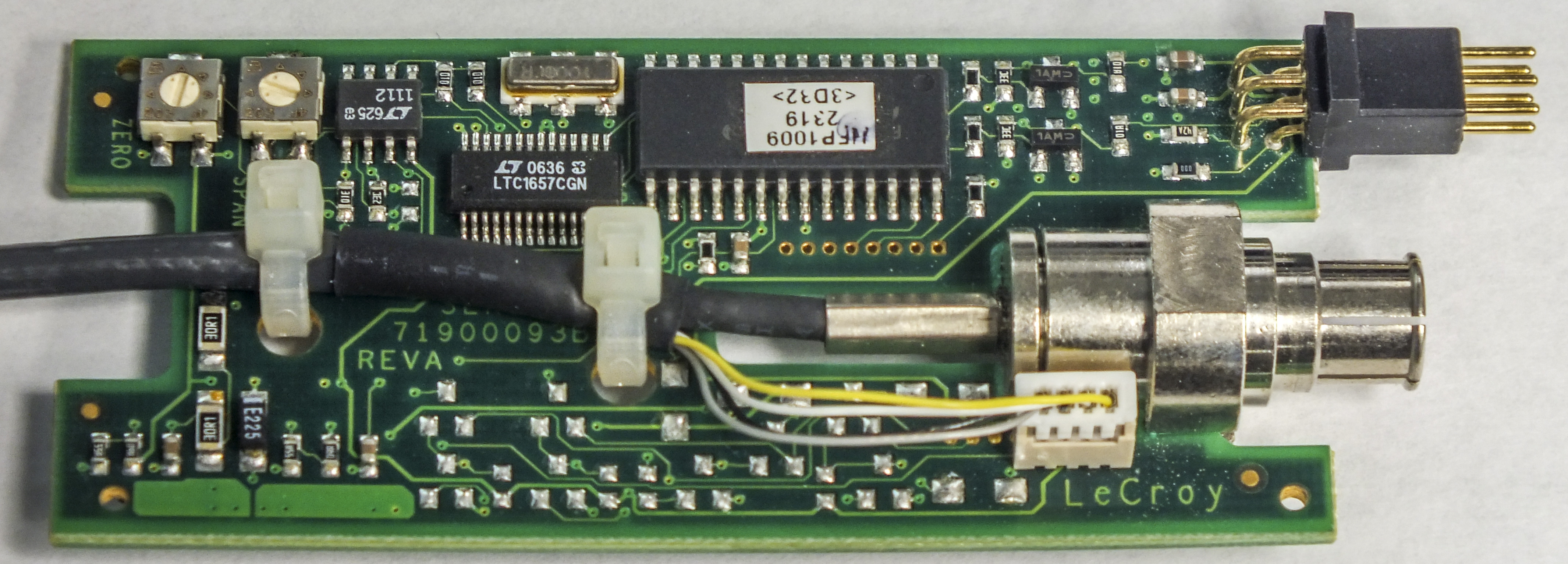
Image 5: Probe body PCBA, top side closeup
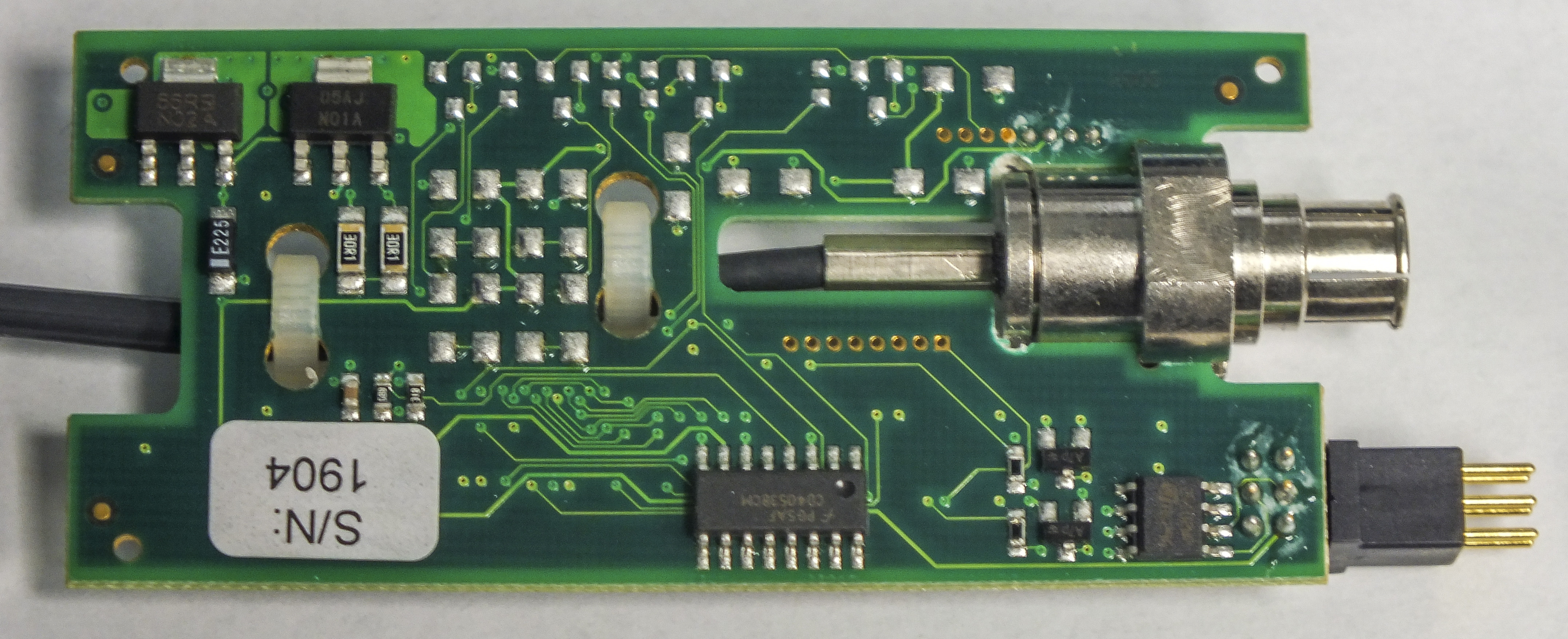
Image 6: Probe body PCBA, bottom side closeup
The underside of the board contains a CD4049 inverting buffer, a ST 24C02 I2C EEPROM, and two unidentified SOT223-3 components which are likely linear voltage regulators. Numerous unpopulated pads are present, suggesting that this PCB may be used for multiple probe variants with different bias voltage requirements.
The top side contains two trimmers labeled "ZERO" and "SPAN", an LT1112 dual op-amp, a LTC1657 16-bit DAC, and a large IC as well as numerous passives and two discrete transistors.
The visible portion of the large IC appears to contain markings for a Microchip PIC microcontroller, however no attempt was made to remove the label to perform an exact part identification.
The DAC is presumably used for offset control, however full circuit reverse-engineering was not performed.
Handpiece
The probe handpiece is a single molded plastic shell which appears to have been slid over the amplifier board, then filled with a black, rubbery-looking potting compound. Several fill holes are visible on the side of the body which were presumably used for injection of the potting. No attempt was made to dismantle the handpiece as this probe was still in active lab service.
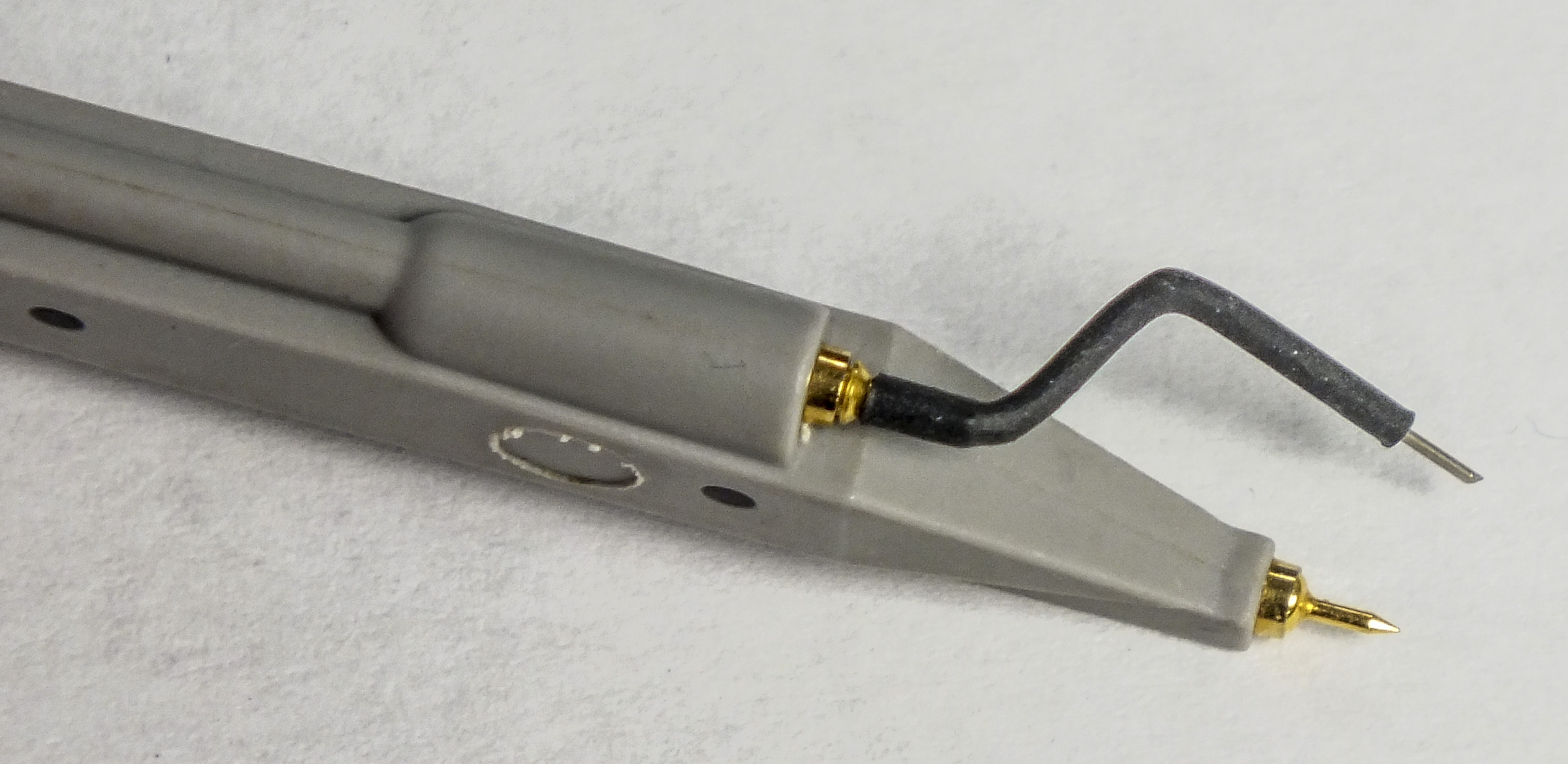
Image 7: Hand piece with the “business” end
A huge range of tips and accessories are provided, which fit the round pin sockets on the handpiece. These include straight, bent, and pogo tips, several styles of ground blade, micro clips, and long flexible ground leads. Many of the longer, more inductive accessories, while they may be ergonomically convenient to use, have detrimental effects on higher speed signal quality due to parasitic effects. They’re still nice to have, given that this probe excels at testing high-impedance low-speed signals.
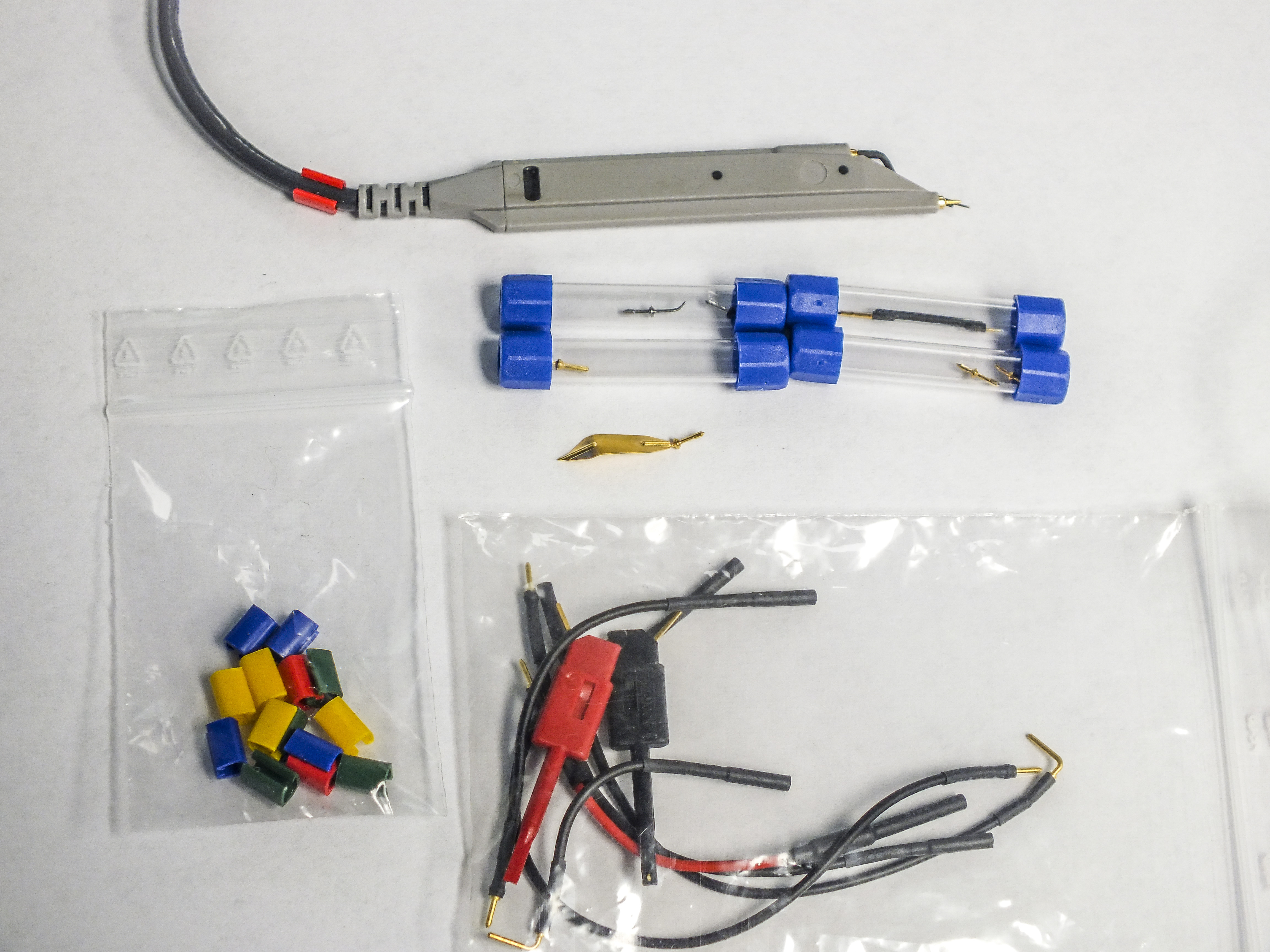
Image 8: Accessories supplied with the probe
Performance
Several performance tests were conducted on the probe using a Teledyne LeCroy WaveRunner 8404M-MS 4 GHz oscilloscope, a Picotech PicoVNA 106 300 kHz – 6 GHz VNA, and a Leo Bodnar 40ps BNC pulse generator, a Rohde&Schwarz HMC8042 power supply, a Rohde&Schwarz HMC8012 5¾-digit multimeter.
All measurements used the "leaf" ground, which provides the best signal integrity according to both the manual and experimental testing.
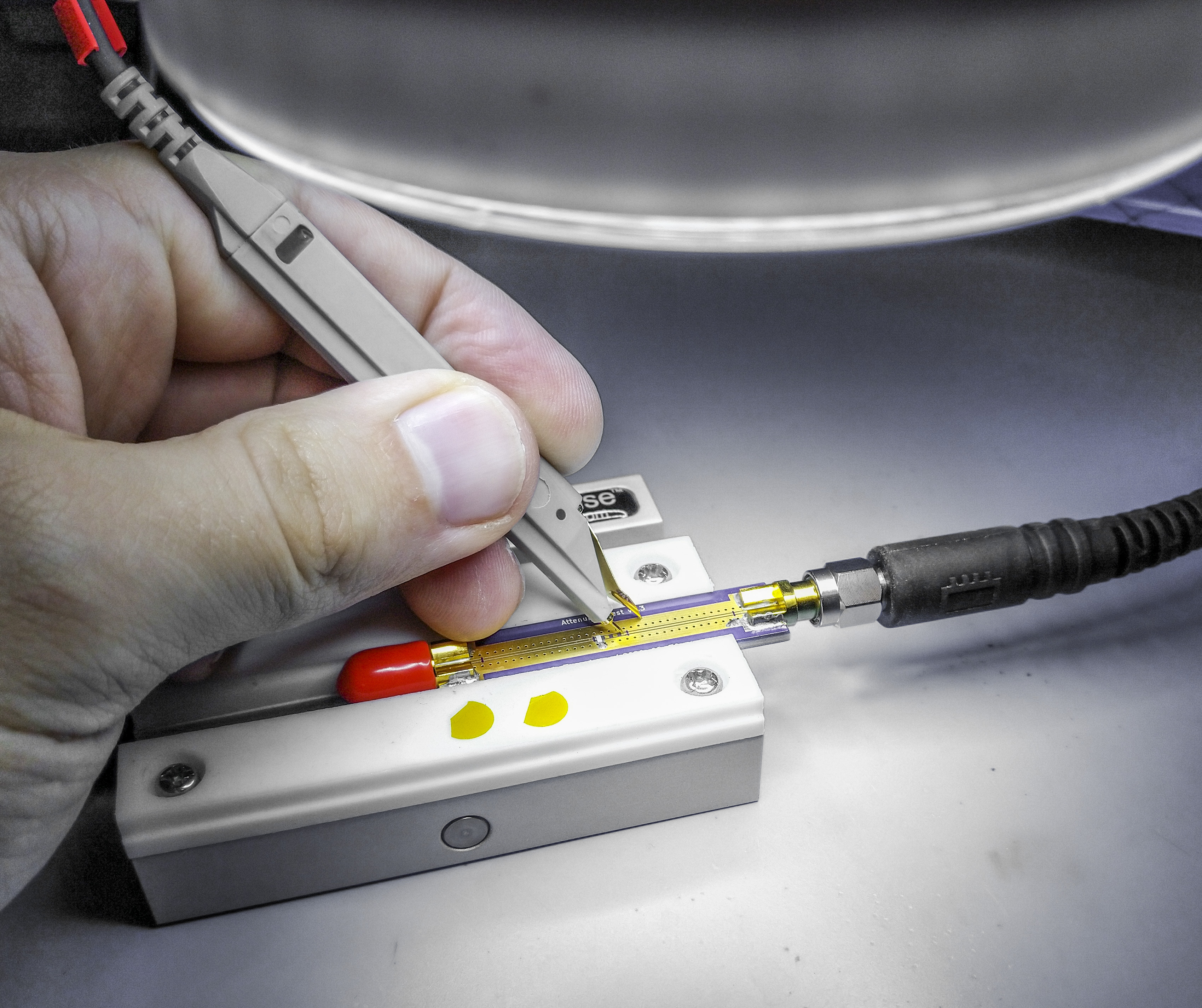
Image 9: Fixture used to characterize probe performance
The overall signal quality through the probe appeared good with no significant artifacts. A very slight dip was visible for about 1 ns after the rising edge.

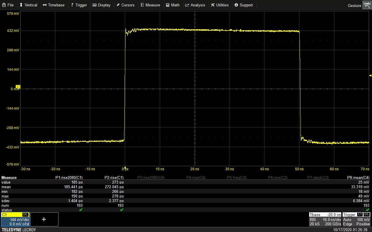
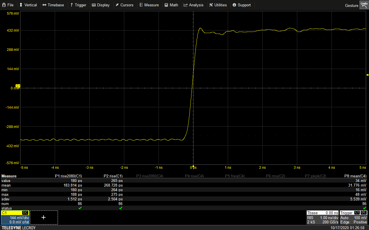
Image 10-12: Measurements with pulse response
It was determined that the probe could be powered up independently of the oscilloscope by connecting +12V to the top left, -12V to the bottom left, and ground to the bottom right pin (as seen looking into the socket on the oscilloscope, not the probe).
When the probe was first powered up into a high-impedance load (the multimeter), both the positive and negative rails drew about 90 mA and the output had a huge offset of around -7.8V, although this slowly drifted toward zero over time. When a 50Ω termination was connected across the output, current consumption decreased to approximately 40 mA per rail, and the output offset decreased to a more reasonable -113.59 mV with the probe tip grounded. The reason for this behavior is unknown, as the actual amplifier circuit is inside the potted probe handpiece and could not be inspected.
This offset was visible when the probe’s BNC output was connected to the oscilloscope via a cable, but not when the probe was connected to the instrument via the full ProBus link. This suggests that the oscilloscope calibrates out this offset, most likely by programming correction values into the DAC. DC gain appeared to be fairly close to 0.1V/V (10x attenuation) however high resolution DC characterization was not performed.
Full 2-port S-parameters from 300 kHz to 6 GHz were taken with the probe across both an open circuit and a 50Ω termination. The probe output was provided with a 50Ω DC load connected to the power tap of the VNA’s integrated bias tee, as earlier testing suggested that this DC load was crucial for correct functioning. During the crossover region below about 5 MHz this DC load and the VNA’s internal AC-coupled termination appeared in parallel, causing a dip in the response which is not present when the probe is only presented with a 50Ω DC coupled termination as provided by a ProBus oscilloscope.
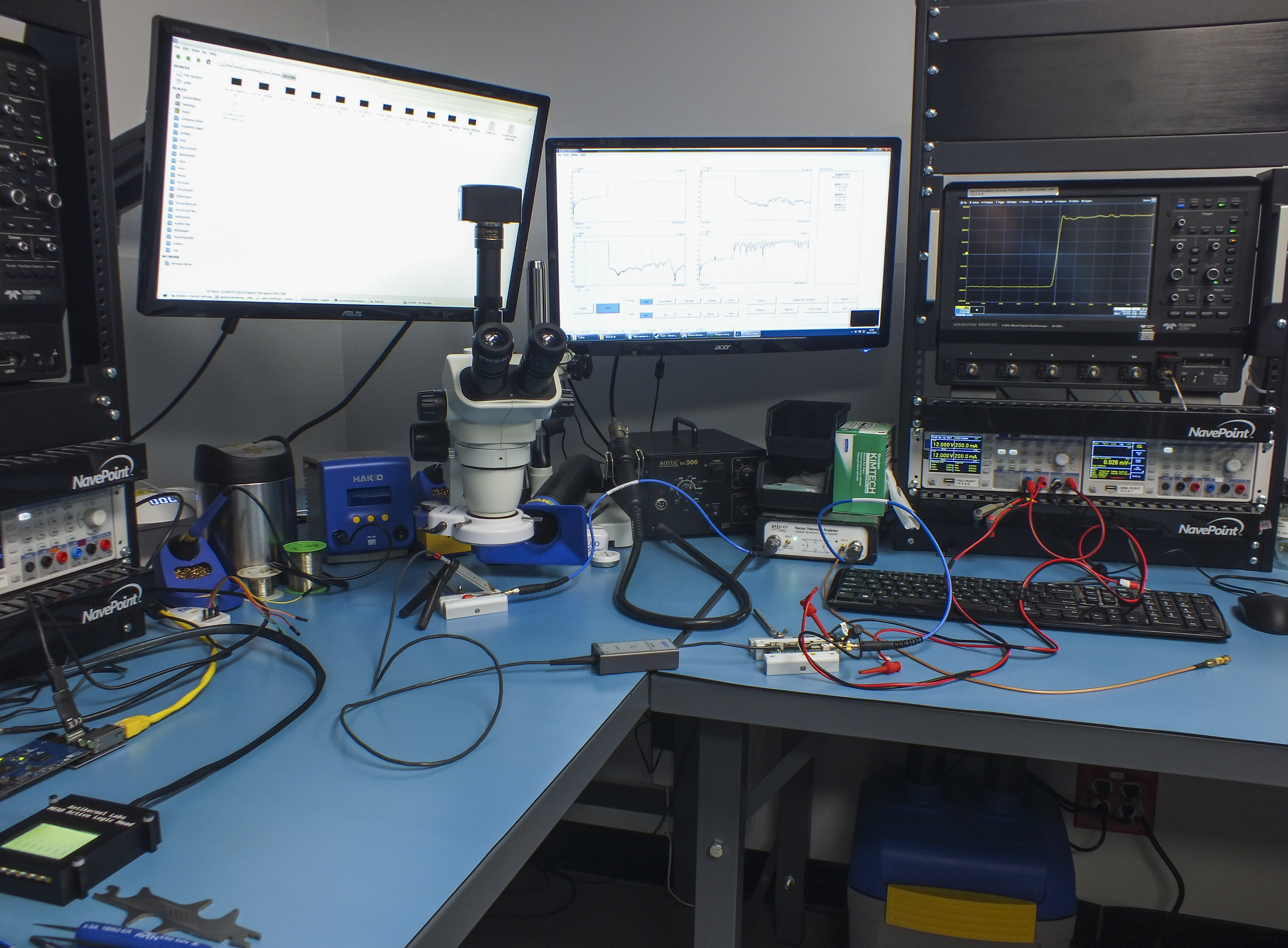
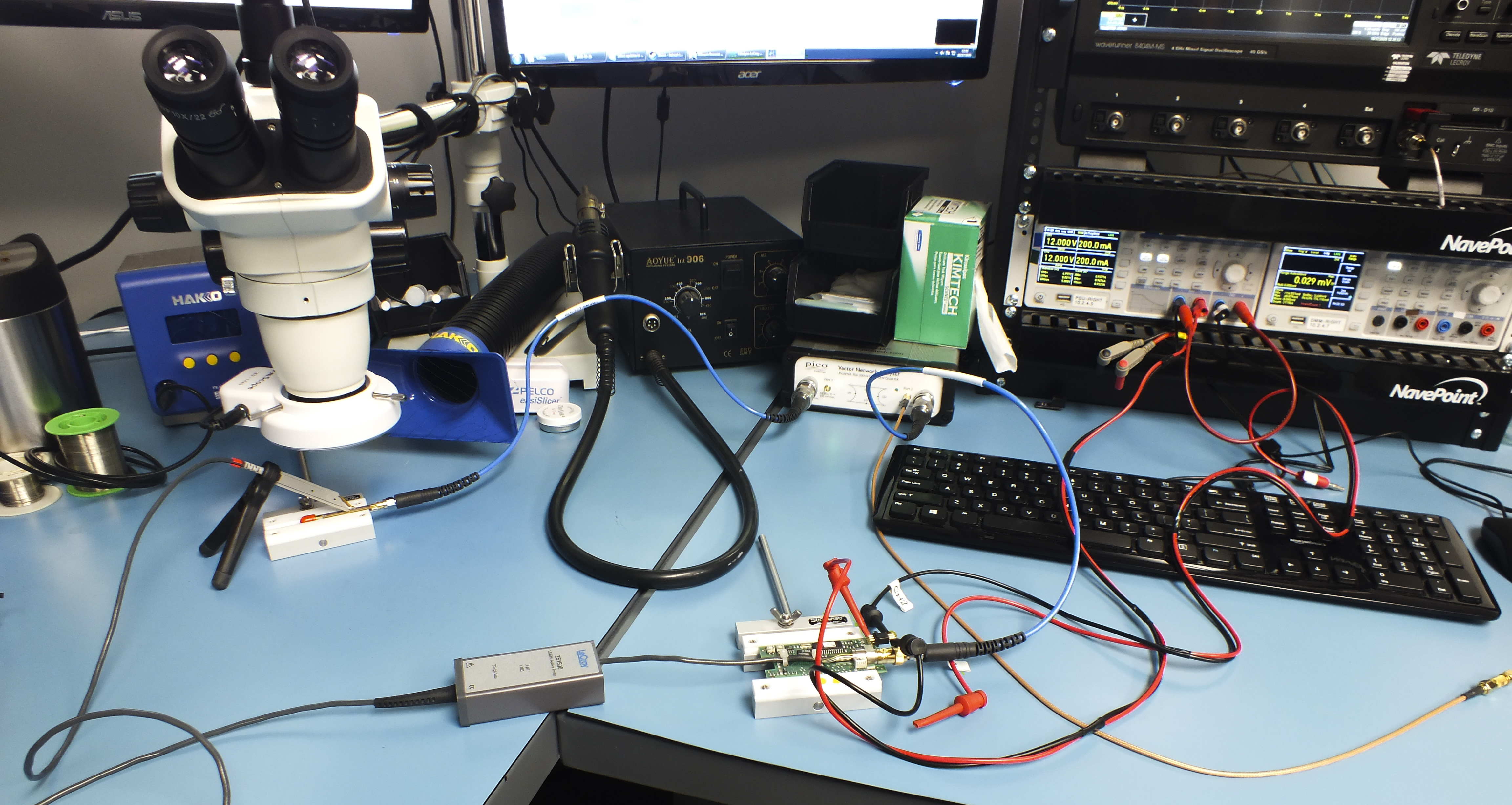
Image 13-14: Measurement setup with VNA
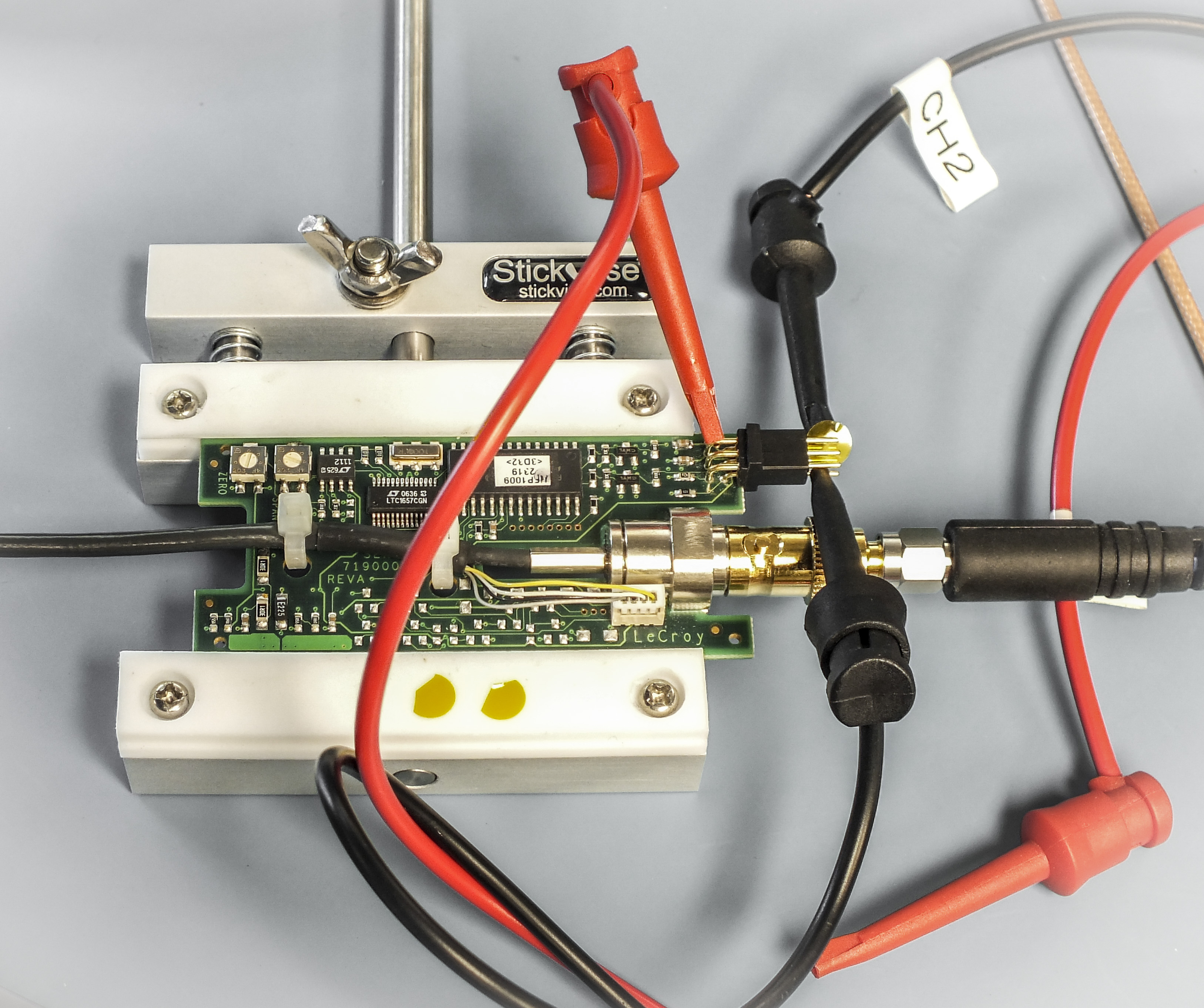
Image 15: VNA fixture with probe contact points
The S21 curve of the probe across a termination showed the expected <5 MHz loss from the experimental setup, then a relatively linear roll off from the nominal insertion loss to the -3 dB bandwidth at 1.21 GHz. At this point the response dropped sharply, reaching -7.5 dB below nominal at 1.36 GHz.
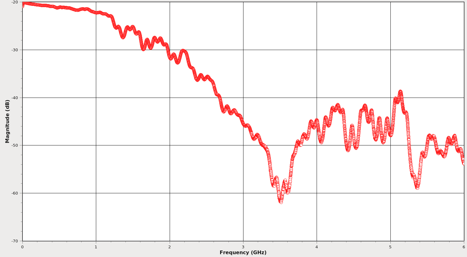
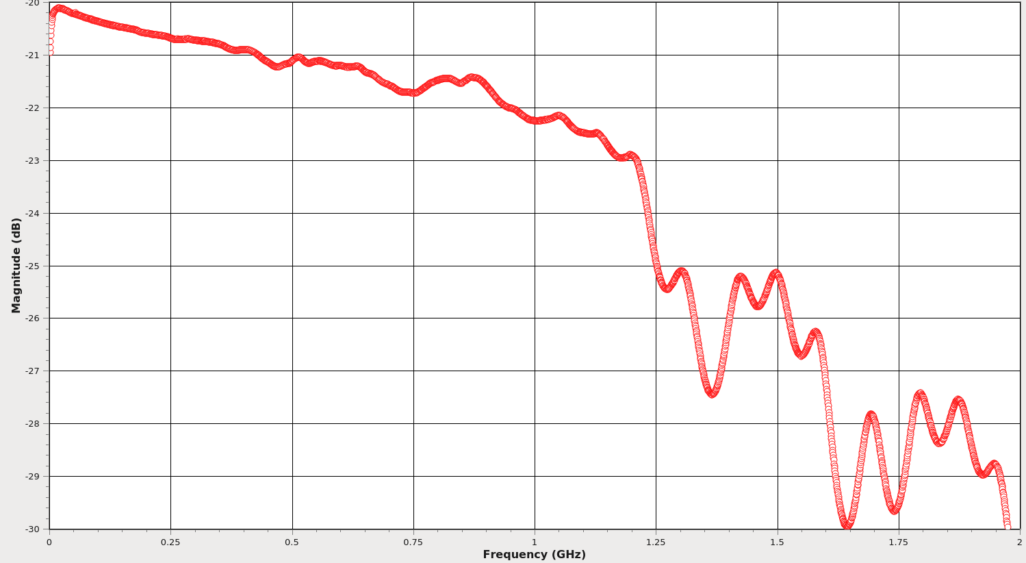
Image 16-17: S21 results
The S11 curve (red) showed very high DC impedance as expected of an active probe, then a steady rolloff to -4 dB at 1 GHz and -8.5 dB at 2 GHz. This highlights one of the limitations of common active probe designs: while they have very low loading at DC, loading can be considerable at higher frequencies. When probing signals with significant frequency content beyond around 500 MHz, a transmission line probe like the PicoConnect 921 (blue), which trades higher DC loading for flatter response, may be a better choice.

Image 18: S11 results
This loading can be seen clearly in the time domain in the scope trace on Image 19.

Image 19: 1.25 Gbps lane link signal demonstration
A 1.25 Gbps repeating 8B/10B pattern was fed through a short length of grounded coplanar waveguide into the scope (M1/M2), then compared to the same signal with probe loading (C2) and as seen through the probe (C4).
S-parameters across open circuit
Conclusions
The ZS1500 generally lives up to expectations for an entry-level active probe. It’s not a probe you’d use for signal integrity work on 10GbE Ethernet, but it’s not priced like one either.
It’s an older design and probably not worth buying new, but if you can find a refurb for a good price it will serve you well. It has significantly lower loading and higher bandwidth than a standard passive probe across the entire operating range, and has lower loading than typical transmission line probes below about 500 MHz.
While it’s not the most frequently used probe in my lab, it sees routine use for probing sensitive lower-speed signals like crystal oscillators.
Redistribution
This article and accompanying data may be freely published and redistributed under the Creative Commons Attribution 4.0 International license (CC BY 4.0).
Discussion about this article and related stuff is welcome in comment section or at our own IRC chat server: irc.xdevs.com (standard port 6667, channel: #xDevs.com). Web-interface for access mirrored on this page..
Projects like this are born from passion and a desire to share how things work. Education is the foundation of a healthy society - especially important in today's volatile world. xDevs began as a personal project notepad in Kherson, Ukraine back in 2008 and has grown with support of passionate readers just like you. There are no (and never will be) any ads, sponsors or shareholders behind xDevs.com, just a commitment to inspire and help learning. If you are in a position to help others like us, please consider supporting xDevs.com’s home-country Ukraine in its defense of freedom to speak, freedom to live in peace and freedom to choose their way. You can use official site to support Ukraine – United24 or Help99. Every cent counts.
Modified: Oct. 18, 2020, 5:41 a.m.