Image 1: Introduction to EVGA Z390 DARK OC Guide
Intro
In this guide we will look at the 2019 EVGA Z390 DARK, representing mainstream Intel 9th Gen Intel® Core™ platform. Key focus points of this DARK motherboard project was delivering maximum performance tuning ability to aid overclocking and enthusiast community. Intel® 9th Gen Intel® Core™ processors are available for quite some time already, with fastest 5.0 GHz Turbo 8-core Core™ i9-9900K processor. This CPU was released in the October 2018, bit over a year since first “i9” model in shape of Core-X series i9-7980XE on flagship HEDT platform. While architecture of this CPU is same as older i7-8700K from end of 2017, new CPU got better core count, more cache and faster clocks. It also have security mitigations in hardware for Meltdown Variant 3 and Variant 5.
Table 1 provides brief feature comparison between Z390 and big brother, HEDT X299 DARK motherboards.
| Feature | EVGA Z390 DARK | EVGA X299 DARK |
|---|---|---|
| CPU Support | FCLGA1151 CoffeeLake-S | FCLGA2066 Kabylake-X/Skylake-X |
| LGA Socket ILM type | Standard ILM assembly | Dual-purpose backplane for custom cooling |
| CPU Power VRM | 12-phase Intersil with 60A Smart PowerStages | |
| CPU Power input connectors | Right-angle Dual 8-pin | Dual 8-pin |
| Overclocking support | Air/water and LN2 Extreme OC | |
| BCLK Overclocking | External IDT Clockgen with fine control | |
| DRAM Support | 2 DDR4 UDIMM High-speed | 4 DDR4 UDIMM |
| PCIe x16 mechanical slots | 3 | 5 |
| PCIe x4 mechanical slots | 1 (can support x16 card) | 1 |
| PCIe x1 mechanical slots | 0 | 0 |
| SLI Support | 3-way | 4-way (Skylake-X i9) |
| NVMe PCIe storage support | 2 x M.2, 1 x U.2 | 2 x M.2 , 2 x U.2 |
| Intel CPU RAID VROC | No | Yes |
| SATA storage support | 8 ports (6 native PCH + 2 legacy) | |
| PCH SATA RAID support | Yes, RAID0, RAID1, RAID5 and RAID10 | |
| Networking | 1 x i219 PHY + 1 x i210AT MAC | |
| USB 2.0 (480 Mbps/port) | 4 via USB Hub | 4 x PCH |
| USB 3.0 (5 Gbps/port) | 6 x I/O, 2 x Header | |
| USB 3.1 (10 Gbps/port) | 4 x I/O + ASMedia ASM2142, Type-A + Type-C | ASMedia ASM2142, Type-A + Type-C |
| WiFi functionality | M.2 Socket 1 Key-E, preinstalled Intel® Wireless-AC 9260 | M.2 Socket 1 Key-E |
| Audio codec | Creative CA0123 | |
| RGB LED support | None | |
| BIOS chips available | Triple BIOS | |
| CPU-less BIOS update | Yes, via dedicated USB port | No |
| CPU HW Slow Mode switch | Yes | No |
| ProbeIt header for DMM monitor | 2 | 1 |
| Legacy OS support | Yes, WinXP+ | Yes, Legacy SATA ASM1061, PS/2 KB |
| FAN/pump support | 8 headers | 7 headers |
| PCB material design | 10-layer high-speed FR4 | 12-layer high-speed FR4 |
| MSRP | $500 USD | $500 USD |
Table 1: Introduction to EVGA Z390 DARK in comparison to X299 DARK
Warnings & Disclaimers
Consider everything below as “educational material” and provided AS IS to aid in the understanding of the true power of your shiny new Z390 system. Proceed with caution and at your own risk as only you are responsible for the possible outcome of out of spec stress. Overvoltage and overclocking voids you Intel CPU warranty.
Overclocking/overvoltaging your EVGA DARK board on any type of the cooling is usually safe for the hardware, as long as it’s done correctly. Always pay attention to details and do some online research on these topics before doing any tuning alterations.
Patience, attention to details and changing things in small steps is key for successful overclocking. Testing stability and performance after each and every modification will provide the best user experience while keeping your hardware safe and always benching over and over again.
EVGA is OK with end user replacing onboard heatsink, product warranty is still preserved. However warranty applies if the device still kept in perfect physical shape, does not have any mechanical damages and reverted to stock condition at the time of RMA. XOC is not covered by warranty and RMA inspection along with secret circuitry onboard can reveal extreme OC conditions history. Always be honest and responsible of your actions with this enthusiast product.
Data provided in this guide was verified on multiple produduction boards, but slight variations in numbers or results for your specific system are still very possible due to silicon variances in samples, different software versions, and benchmarking applications.
EVGA Z390 DARK Series features
Z390 is 4th “DARK” motherboard from EVGA with ultimate performance on any type of cooling as the top priority goal. The DARK series motherboards, similar to EVGA KINGPIN Edition graphic cards are made to get the performance records broken. Z390 continue on X299 DARK’s legacy, further adding CoffeeLake-S processor support into series. First X79 DARK was introduced in 2013 as first board to carry this classification. Today DARK replaced former Classified series and is top of the line offering for performance.
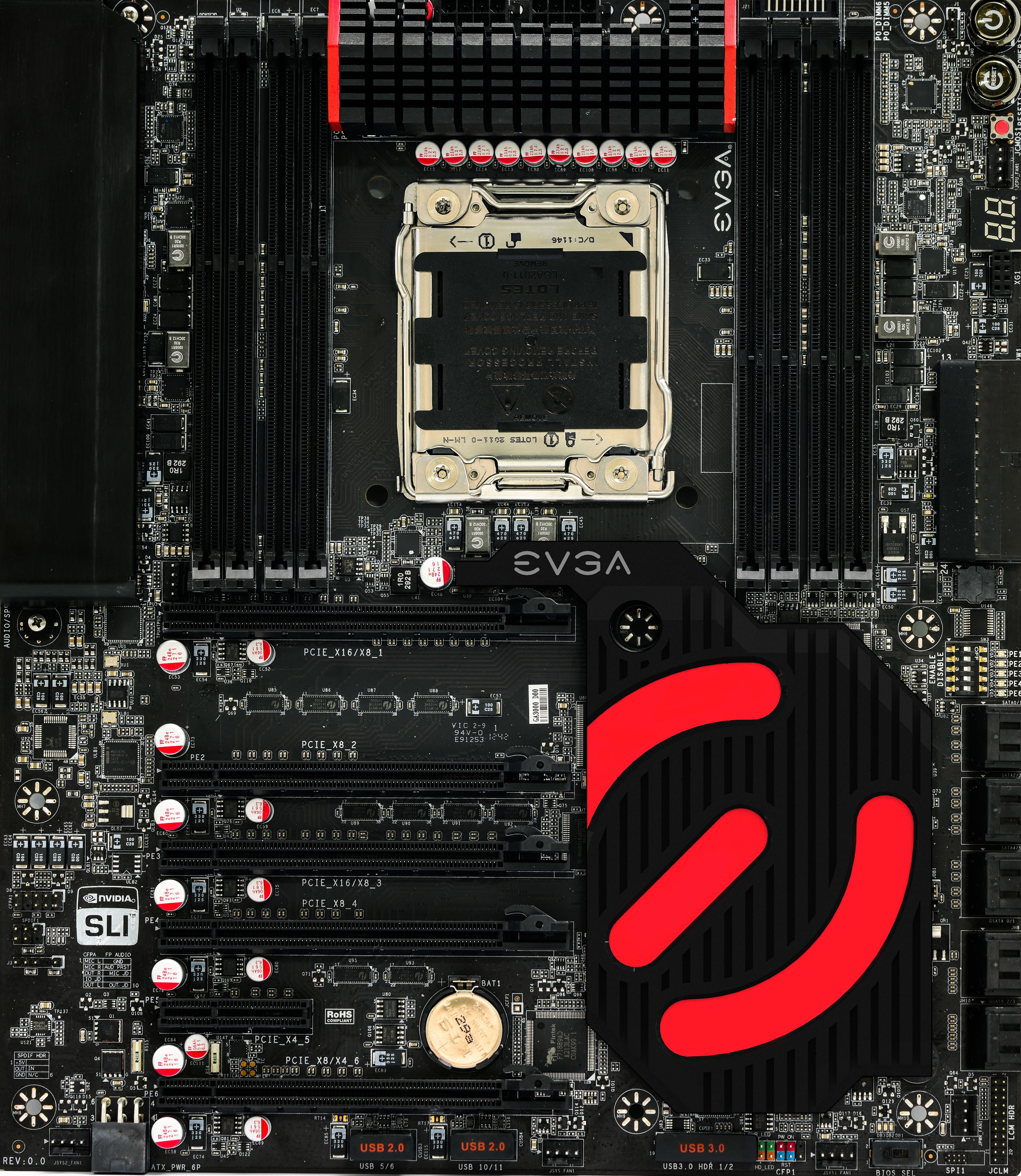
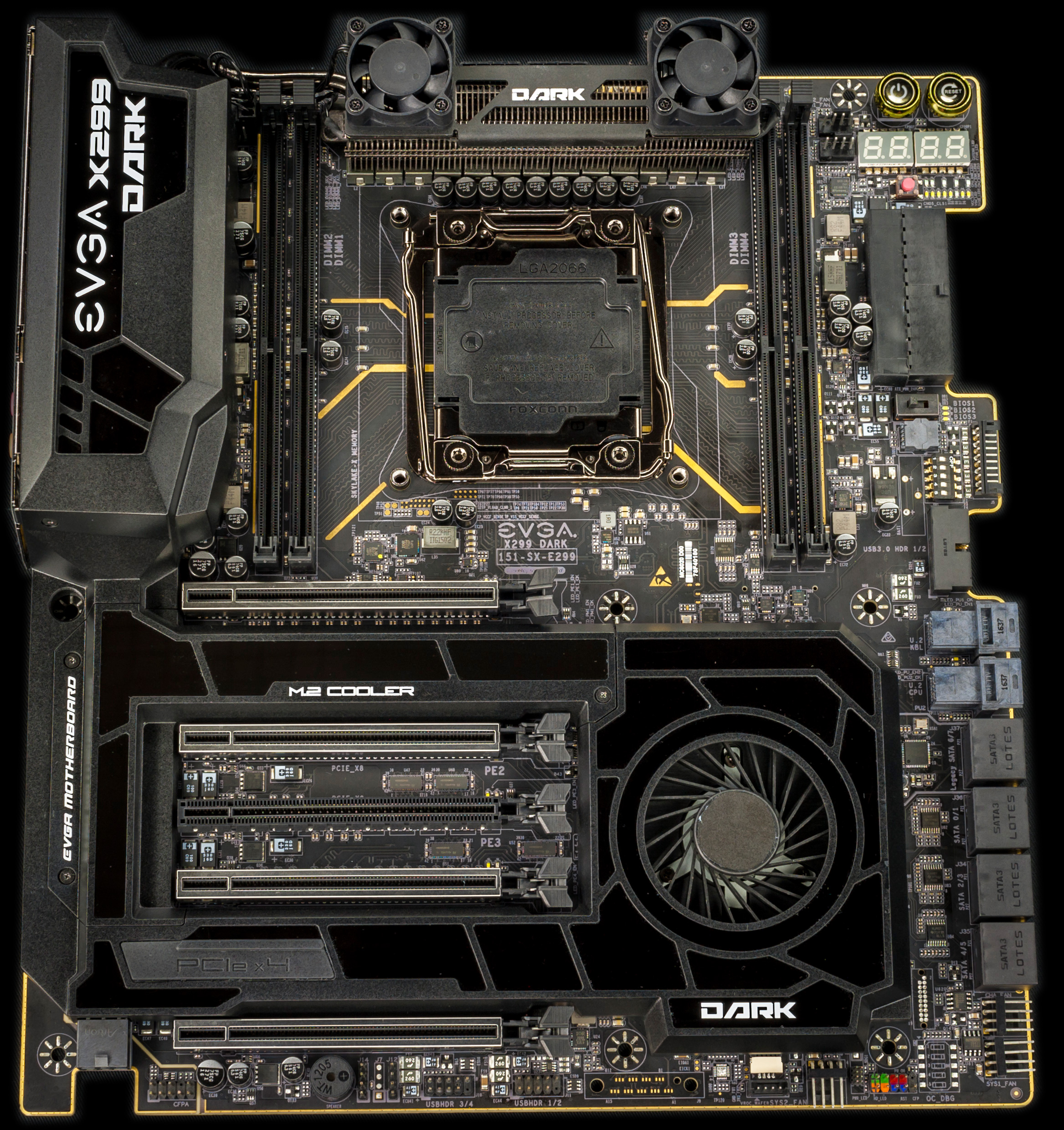
Image 2-3: DARK series boards: First EVGA X79 and third EVGA X299
Yes, you got that right, second DARK board in series is not shown. It is so secret and special, that there are only two boards in the whole world. I can only say that it’s based around Intel’s X99 chipset and working with Core i7-6950X processor and only handful of people seen it in flesh. However today we talking about CoffeeLake K-series mainstream platform, and it’s time we get back to Z390 realms.
Z390 DARK, just like X299 predecessor deprived of the bling, focusing on the performance above all. There are no RGB LEDs or fancy displays here. All money invested into high performance PCB material, design, power regulation circuitry and hardware monitoring/fine-tuning flexibility.
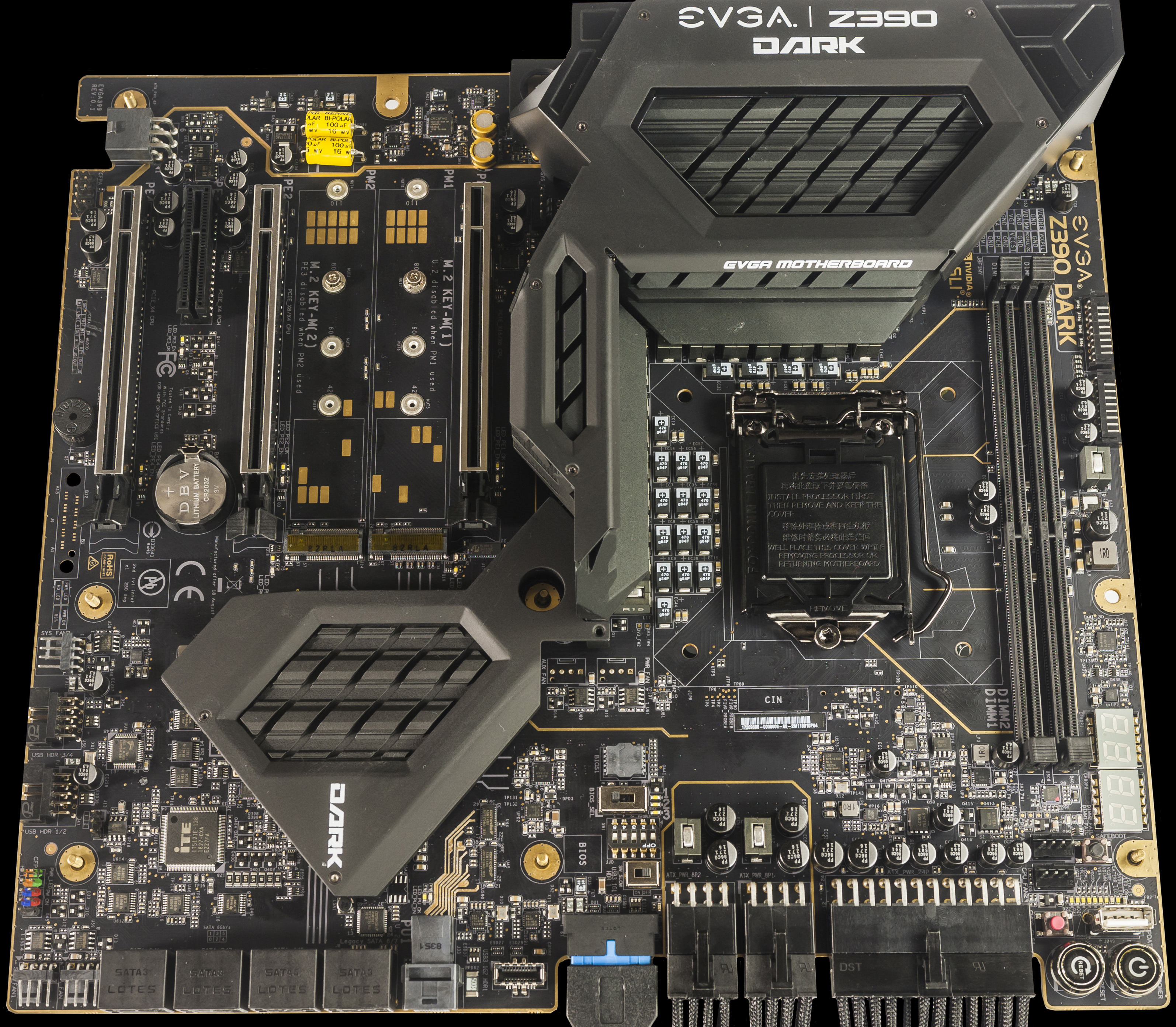
Image 4: EVGA Z390 DARK Motherboard in retail configuration
It’s a full ATX size with dimensions measuring 304.8 × 276.7 mm. This is slightly more than typical ATX board, but well within limits of full-size 304.8 × 304.8 mm EATX form-factor dimensions.
LGA1151 CPU socket together with two DDR4 UDIMM slots oriented in parallel with PCIe slots. We have chosen such orientation to allow placement of dual 8-pin MiniFit Jr. power connectors for +12V CPU power next to main 24-pin input. As result CPU VRM is angled between CPU socket and first PCIe slot to reduce impact from longer distance between power entry and VRM. Also this reminds good old DFI LanParty NF4-Ultra board in my AMD Socket 939 days.
All but one (USB 3.1) connectors on the right edge are right-angled, to allow for clean cable management. Some cases might lack additional spacing, and to aid this Z390 DARK has cutout for 24-pin ATX and +12V 8pin CPU power entry PSU cables, together with internal USB 3.0 front panel cable.
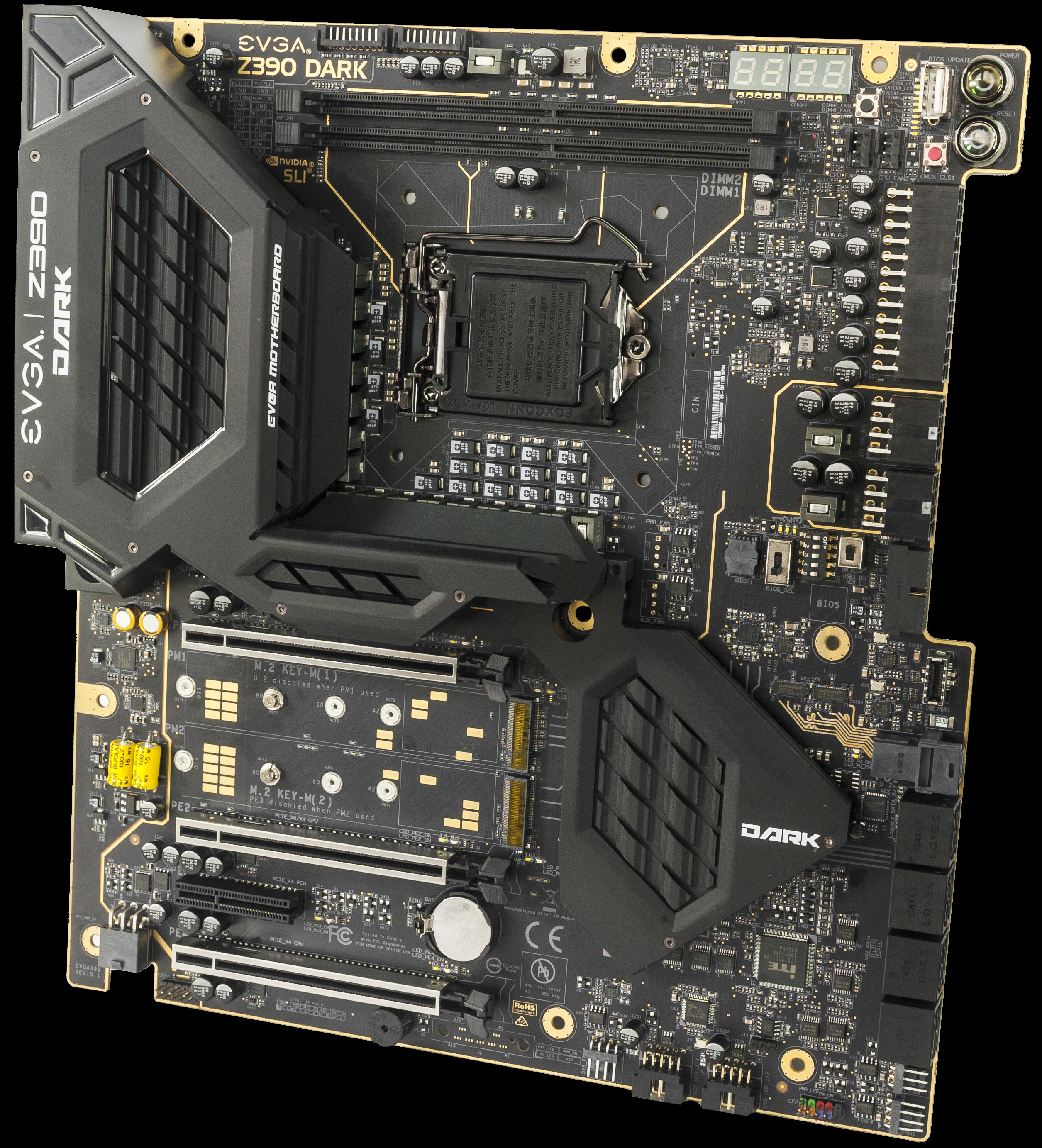
Image 5: EVGA Z390 DARK Motherboard
Z390 platform does not have lots of PCIe lanes. Due to lack of the large amount for lanes first PCIe slot area is instead sacrificed for large passive VRM heatsink, while still supporting three x16 mechanical slots for 2-way SLI functionality. Which is all that RTX cards can do in terms of multi-GPU setups anyway. With 2-way SLI cards will operate in native PCIe Gen3 mode at x8 width. If you need to run 3-way or 4-way SLI with older GTX cards or lot of PCIe SSD drives you’d need to use board like X299 DARK instead. Z390 DARK board does not use expensive PLX PCIe bridge to avoid unwanted delays in PCIe-CPU interface.
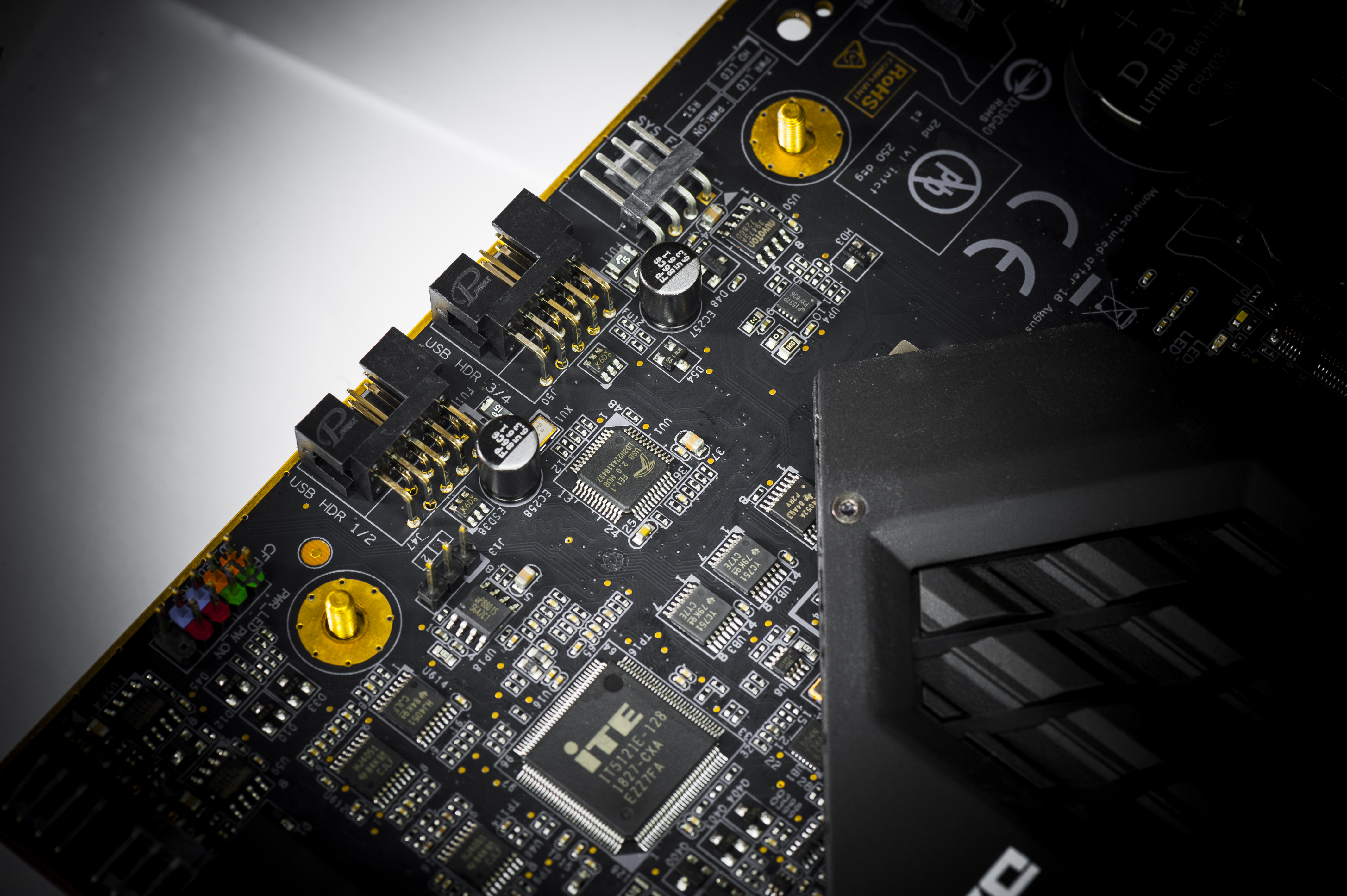
Image 6: USB 2.0 ports from hub and other bottom side connectors
PE2 slot sharing lanes with last PE4 slot, so it will be either x8/x0 or x4/x4 configuration. Rest of the connectivity like M.2 or U.2 ports are routed from Z390 CoffeeLake-H PCH. There is also support for USB PD charging or high power delivery thru rear Type-C and front-panel header USB 3.1 ports.
Bottom row of the chassis connectors feature auxiliary ports in next order (left to right):
- CFPA – front chassis audio connector
- Buzzer – diagnostics buzzer for BIOS testing purposes.
- SYS2_FAN – standard 4-pin right-angle PWM/DC Fan header.
- J50 USBHDR 3/4 – USB 2.0 chassis header for Port 3 and 4
- J47 USBHDR 1/2 – USB 2.0 chassis header for Port 1 and 2
- Chassis header – header for PWR_ON, HDD LED signals and PWR_ON, RESET buttons.
80Port diagnostics, control buttons and switches, BIOS socket – all these user accessible items are located on the top area, so there is no need to remove devices from PCIe slots to reset the board or troubleshoot BIOS settings. Dual ProbeIt header can help with monitoring key important voltages with external DMM. PCIe disable switches help to troubleshoot which slots contain the failed GPU device that prevent system to finish the POST sequence.
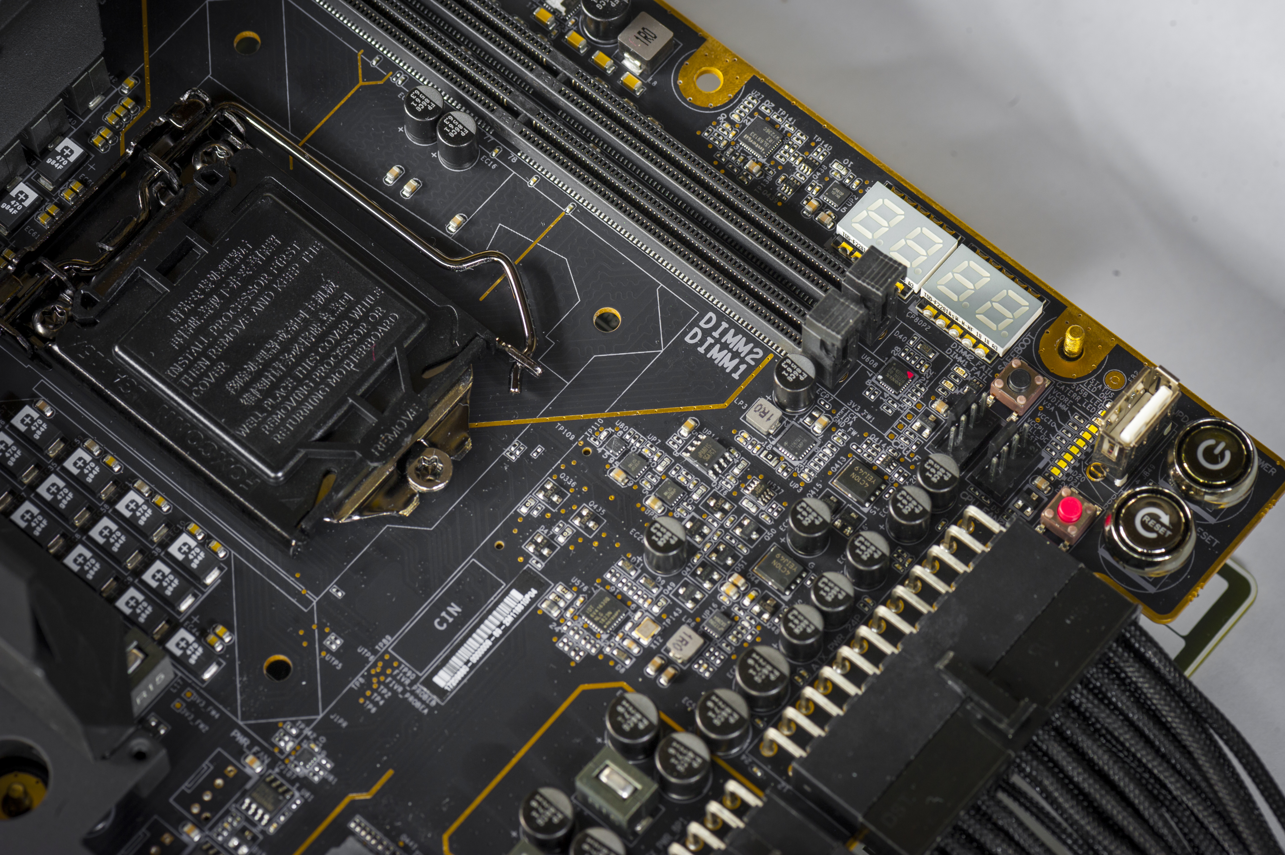
Image 7: Top right corner area on EVGA Z390 DARK
Area around CPU socket using slim tantalum capacitors to simplify extreme OC cooling insulation and setups. I remember wasting lot of time making little cutouts in foam for every capacitors to make a water protection foam gaskets around the socket. Making board easy to use for extreme OC was one of the key focus points during PCB component placement.
Processor support
Mainstream is expanding with new 6/8-core 8th Generation Coffee Lake and 9th Generation Coffee Lake processors Available control items in BIOS GUI are also automatically configured, depending on installed CPU. Board supports all available desktop CoffeeLake architecture CPUs in LGA1151 form-factor.
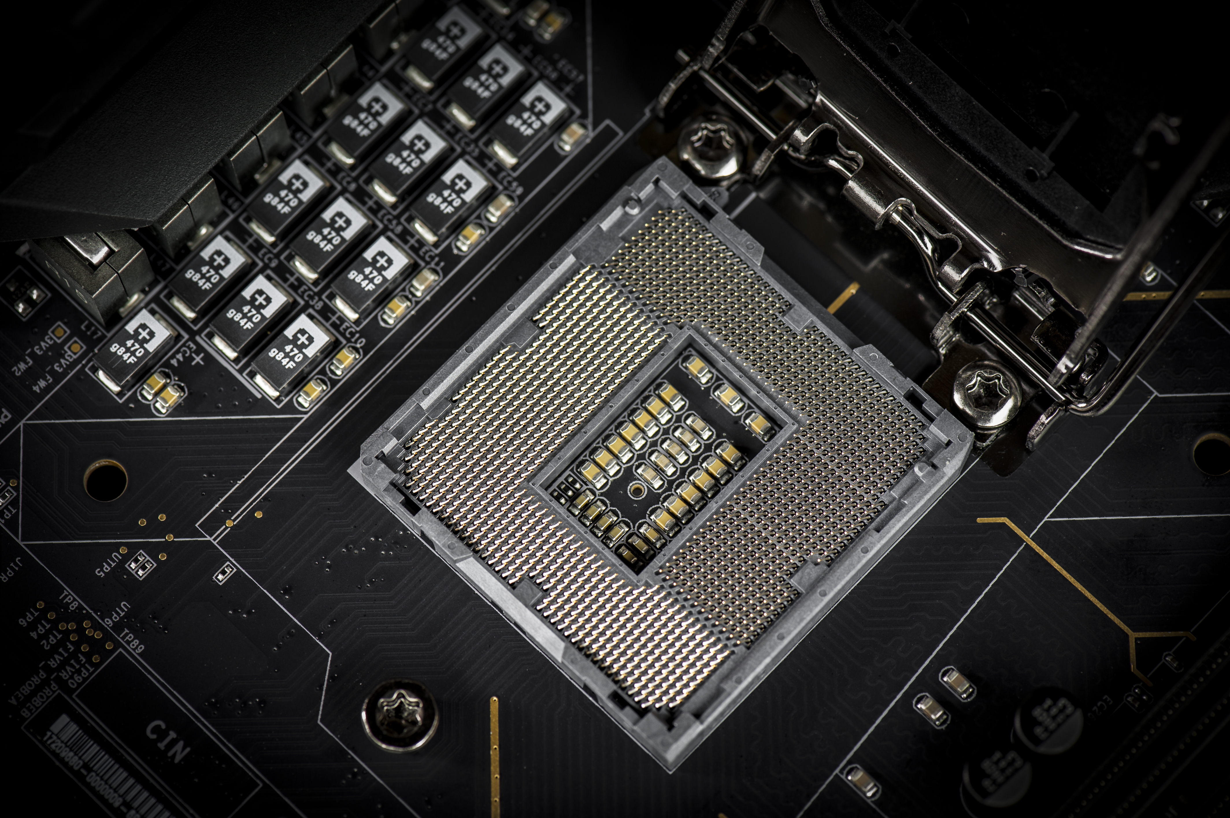
Image 8: Processor socket
Be careful not to touch socket pins under any circumstances. Bent or damaged socket pins are not covered by manufacturer warranty.
Some settings are also automatically adjusted by BIOS depends on the current operation profile. One of such examples – CPU power limits controls. These are usually available in BIOS and tweaking utility in OS, such as Intel XTU. Unlike some other boards, on Z390 DARK you will not find PL1/PL2 (power limit) settings and other power management settings for CPU in BIOS UI. These limits are maintained by BIOS itself to simplify overclocking experience. If you running stock settings then everything follows Intel specifications, but when you do overclocking (that is setting CPU/BCLK ratios and voltages higher than stock defaults) board will take care of power limits, to make sure CPU never throttle, unless you hit temperature limits.
High-speed memory layout
Good memory performance requires good high-speed PCB layout and routing specifications. Additional PCB layers, signal shielding and power quality are all factors that greatly influence the system memory performance. Also leaving hardware alone no overclocking can happen without good BIOS tuning and tweaking the correct settings. Additional loading to the signals, in form of extra connectors also negatively impact maximum DDR4 frequency.
Hence on DARK amount of memory slots is reduced to only one per channel, with total 2 DIMMs. Modules with 16 Gbit memory IC density such as 32GB UDIMM are also planned to full support. EVGA Z390 FTW board offer 4 DIMM for the users than need memory capacity larger than 64 GB.
As interfaces and signals go faster, digital design for error-free operation become a challenge. With memory clocks reaching more than 4000 MHz various physics factors and effects come into play and impact the semiconductors and DDR4 interface operation. Memory speed performance remain the bottleneck due to complex signal integrity issues further amplified with lower signal voltages and higher DRAM density. As we get more processor cores and faster I/O devices, demand for wide memory bandwidth is also getting only stronger. That is one of the reasons why on graphic cards and enterprise market we already see alternative approaches like using HBM memory (AMD Fury and Vega GPUs, NVIDIA Pascal GP100/Volta GV100), MCDRAM (Intel Xeon Phi x200) and HMC in FPGA, HPC markets.
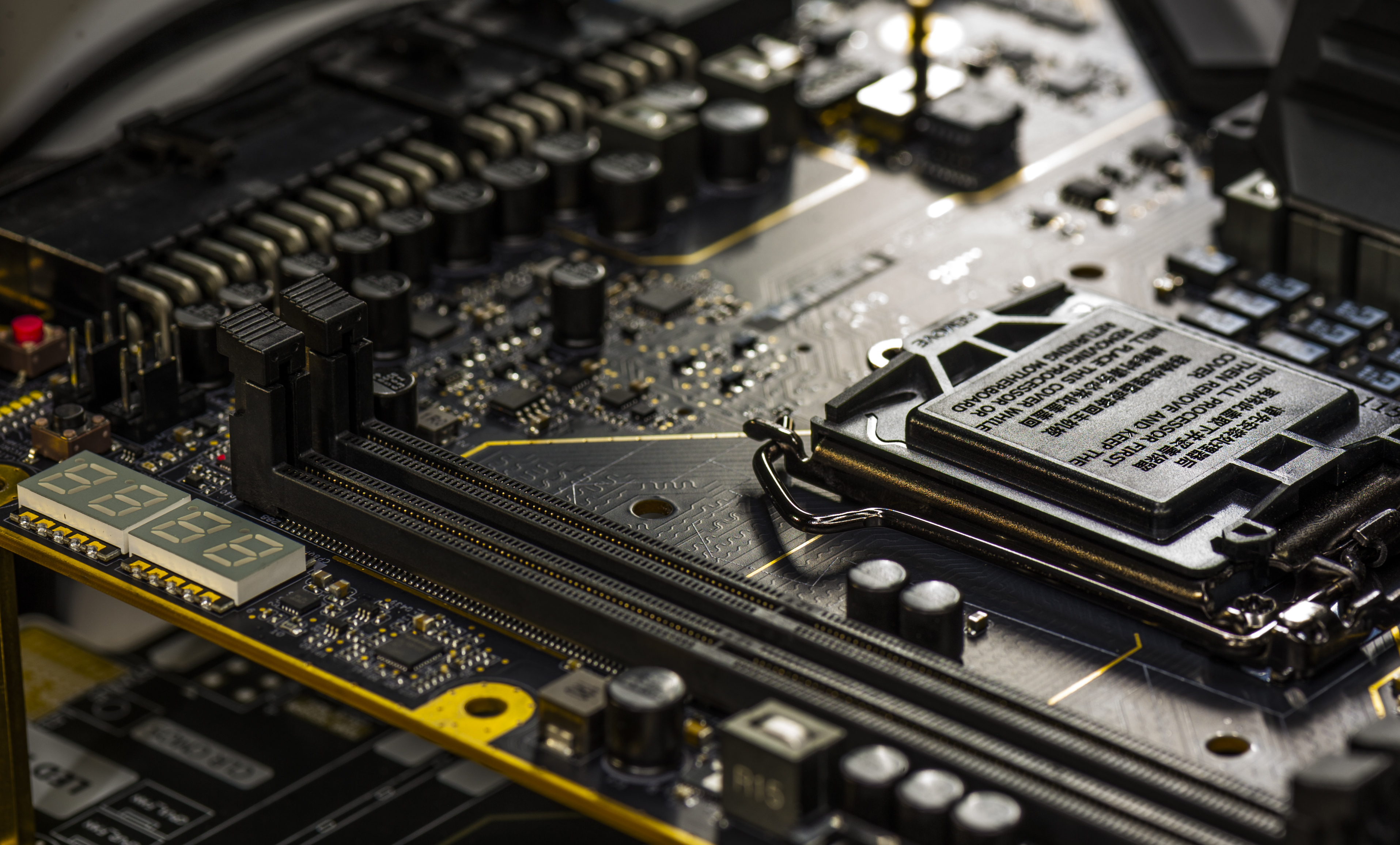
Image 9: DDR slots
Single DIMM slot per channel allows faster clocks, well beyond 4600 MHz with good CPU sample. Typical DDR4 UDIMM today have 8 GByte capacity, which is not a small amount for typical loads. High loading and workstation scenarios that need additional memory have a path to expand with 2 × 32 GByte UDIMM modules, allowing total memory size of 64 GB. However given scarce availability of 16 Gbit density memory most users today have 2 × 8 GB or 2 × 16 GB modules, which are already fully supported.
Great amount of time and effort was dedicated on making automatic XMP operation well for all range of the speeds, including very high frequency ranges like 4400-4800 MHz. All major memory manufacturer has these high-speed modules available, even though real practical benefit is barely (in)visible in any real-life application. Optimum memory speed for high-end Z390 system is around 3800-4200 MHz with good memory timings.
Only unbuffered DDR4 non-ECC DIMMs with capacity up to 16 GBytes/module are supported. Board will not work with server DDR4 RDIMM or LRDIMM modules, no matter what capacity they are.
VRM design overview, available tuning and hardware controls
Power regulator for CPU and memory on EVGA Z390 DARK is based around the brand new Intersil digitally-controlled converter and compact 60ADC Smart Power Stage IC – Intersil ISL99227B. VRM on this board is upsized to 12 phases to handle LN2 extreme overclocking to ensure no limits, even with i9-9900K CPU running over 7.4 GHz with LN2.
All VRM components are passively cooled by massive extruded aluminum heatsink. Due to high efficiency this VRM have good thermal margins even when no airflow available, like in cases with watercooled CPU.
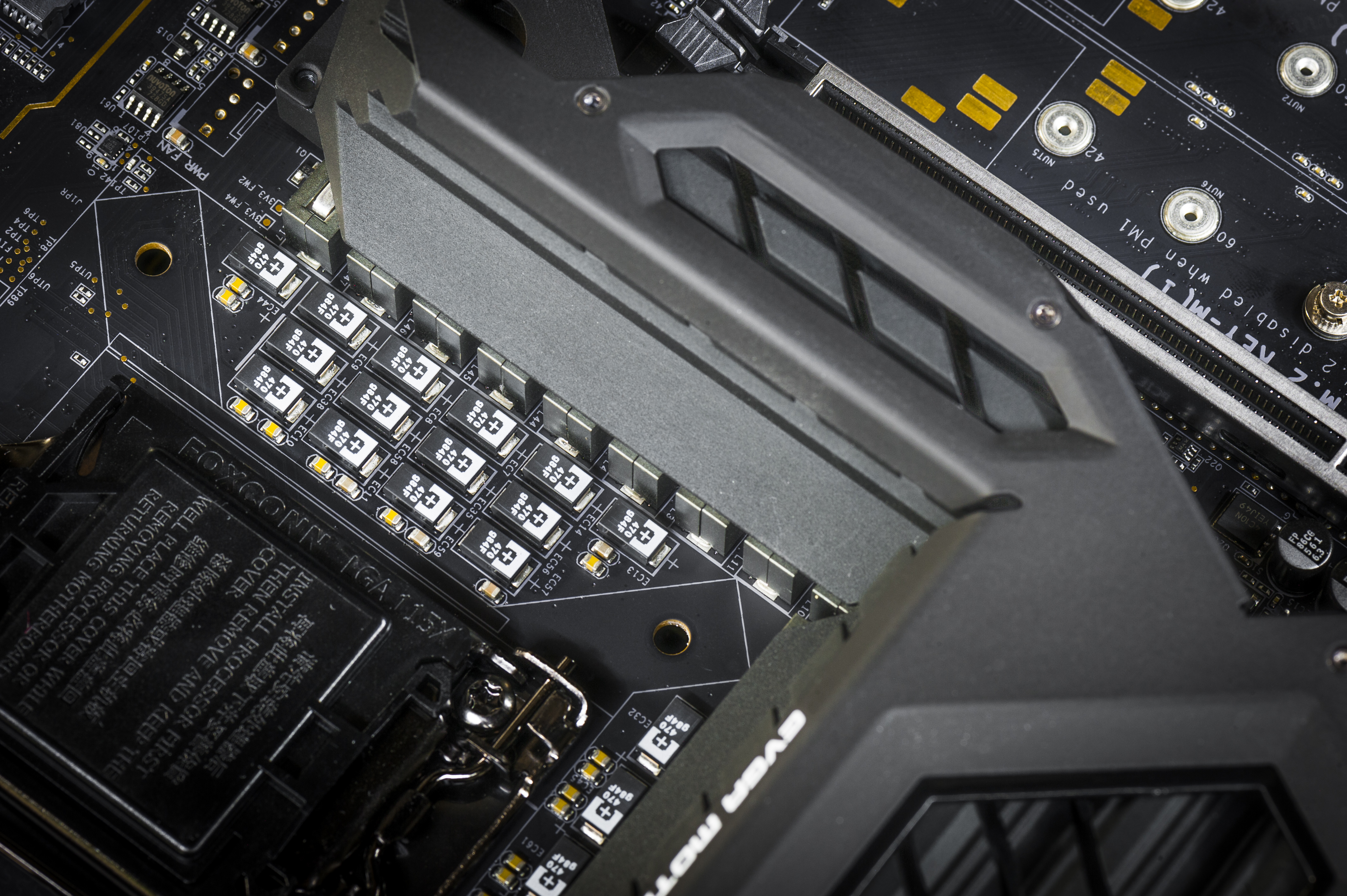
Image 10: VRM cooler and circuits around CPU socket
Main CPU power regulator has 12 phases to meet high current demands for high-end Core i9 K-series processors, even under the exotic cooling conditions and very high CPU voltages.
This very same VRM was first used on X299 DARK, where it powers 18-core 36-thread behemoth processors without breaking sweat. As result 8-core CoffeeLake is very easy job for such VRM, overclocked or not. Great thermal and power headroom avoids need of active airflow, so Z390 cooling solution is completely silent and passive.
Gamers Nexus have nice overview, covering power design aspect of EVGA Z390 DARK motherboard. Be sure to check it out if you like videoformat presentation.
Voltage tuning functionality
Z390 DARK hardware and BIOS provides full control over every available voltage platform has to offer. Digitally controlled 12-phase PWM controller ISL69138 handle VCORE regulation, driving 12 x Intersil ISL99227 60A SmartPowerStages. Similar controllers also handle System Agent (VCCSA) with ISL99140 and VCCIO voltages. Integrated graphics is powered by 2-phase VCCGT, controlled thru PWM controller ISL69133 and pair of ISL99227. Graphics power provided only when it is actually used, and shutdown for rest of the time, saving energy. You can manually force it enabled or disabled as well, using BIOS Setup item.
Almost all voltage settings in BIOS are on the main OC page, as these settings are paramount importance for the successful overclocking on the Z390 DARK. There are multiple settings tailored for VCore, VSA, I/O and PLL voltages. All main controllers on Z390 DARK support digital interface, so we have some advanced controls available here. Memory related voltage controls are moved to MEMORY BIOS page to maintain simple and easy to use layout.
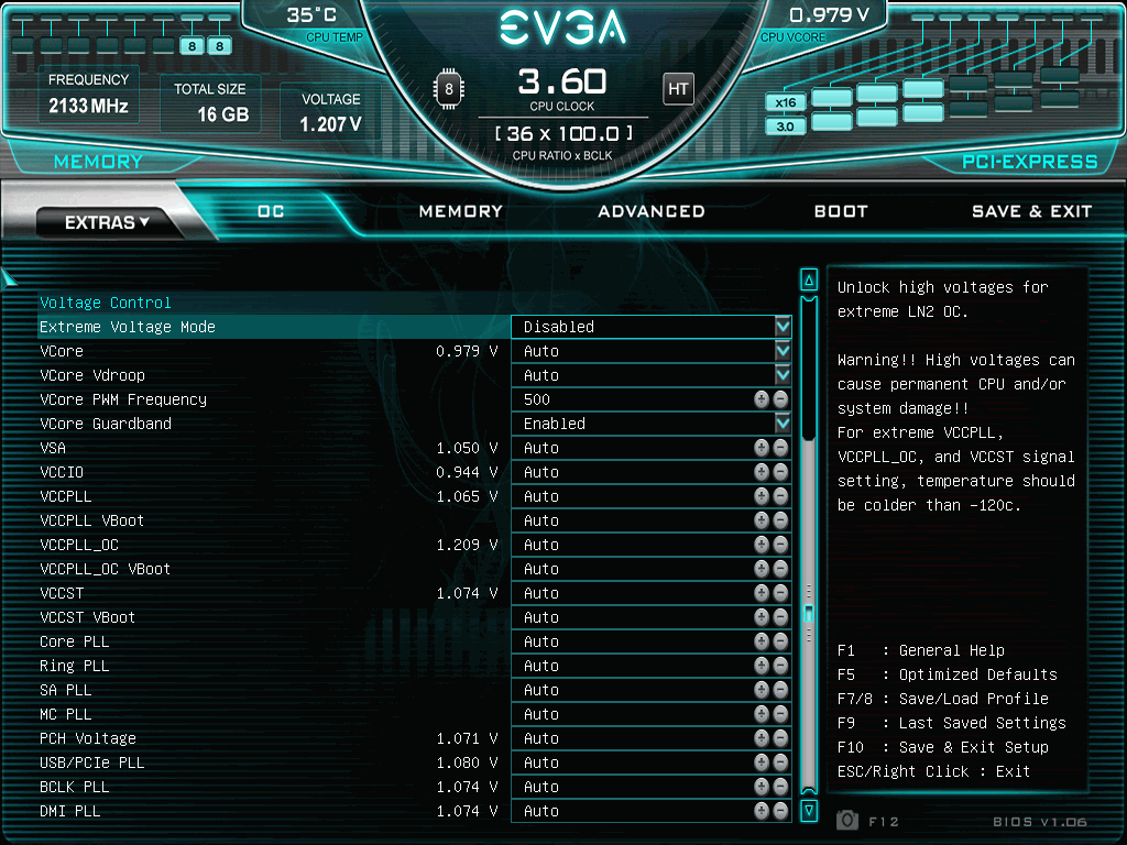
Image 11: DARK BIOS setup menu items
Extreme Voltage mode unlocks high voltage levels for extreme overclocking with dry ice and liquid nitrogen cooling. This settings need to be disabled for all everyday user cases, such as aircooling and watercooling. Using extreme voltage setting for everyday setup can be dangerous to CPU’s life.
VCore VRM have four settings available:
| Setting name in BIOS | Voltage range | Notes |
|---|---|---|
| Vcore | Auto, Adaptive or Override | Main processor voltage, recommended below 1.4V for daily use |
| Vcore Vdroop | Auto and 9 settings | Loadline and Vdroop settings |
| Vcore PWM Frequency | Auto, 400 – 800 kHz | Switching frequency for Vcore, recommended value around 500 kHz |
| Vcore Guardband | Enabled / Disabled | Keep this Enabled to meet Intel VRM specs |
Table 2: CPU Core VRM settings on Z390 DARK
Switching PWM frequency range can be extended up to 1000 kHz, however it’s best to avoid settings over 800 kHz due to high thermal stress on the power delivery circuits.
If thermals are good (below +70 °C on hottest core, under maximum stress) additional Vcore voltage for the processor will usually result higher maximum clock speed able to be achieved. If you after maximum performance at all costs, it is recommended to use the voltage override mode of the cores for fixed voltage level, and bump I/O and System Agent voltage for better memory overclocking performance.
System Agent voltage powers various auxiliary devices and interfaces on CPU, like PCIe and DMI interface.
VCCIO rail provide power to low-speed interfacing, sequencing logic and I/O drivers. This voltage have large impact on memory controller stability, and might need increased levels to allow high BCLK and/or high frequency on memory overclocking. DRAM voltage settings are available separately in the memory tab.
Keep in mind that too high PLL, SA or I/O voltages can also make system unstable or even degrade CPU stability and life. Trying to run system with high voltages without step by step testing would not be a good idea. Graceful methodical approach, testing each setting impact can do wonders when it comes to overclocking and maximizing performance of the system. It is indeed time consuming process, but once you get knowledge how to tune the system right, it’s actually not that hard to do. Many settings and concepts are carried over from older platforms, including X299 and Z170/Z270 systems. And once you learn how to tune Z390 DARK, you will also do great results with future processors/systems too.
VCCPLL, VCCPLL_OC and VCCST voltages are key importance in extreme LN2 overclocking. These voltages/settings have to be set correctly to allow stable operation of the processor under extreme cooling conditions. If voltages are not correct you will see “cold-bug”, meaning failure of processor to operate below certain subzero temperature. Default voltage settings allow CPU to work around -100 °C to -120 °C. Correct voltages on these three domains allow CPU operation and benchmarking even when temperature is -196 °C, with LN2 container full and boiling.
Lot of other PLL settings are available for fine-tune control on various interfaces. These might be helpful to stabilize the system once you figure out correct main voltages for your overclock settings. Default voltages for all of these settings available in BIOS section of this guide.
Realtime voltage monitoring
ProbeIt header is 10 pin interface for external voltmeter or DMM such as this Fluke 106. There are two of these on EVGA Z390 DARK, allowing real-time monitoring of all vital voltages delivered to CPU, completely independent from software. This is handy to check voltage readings during overclocking session and do power checks to make sure everything is nice and stable.
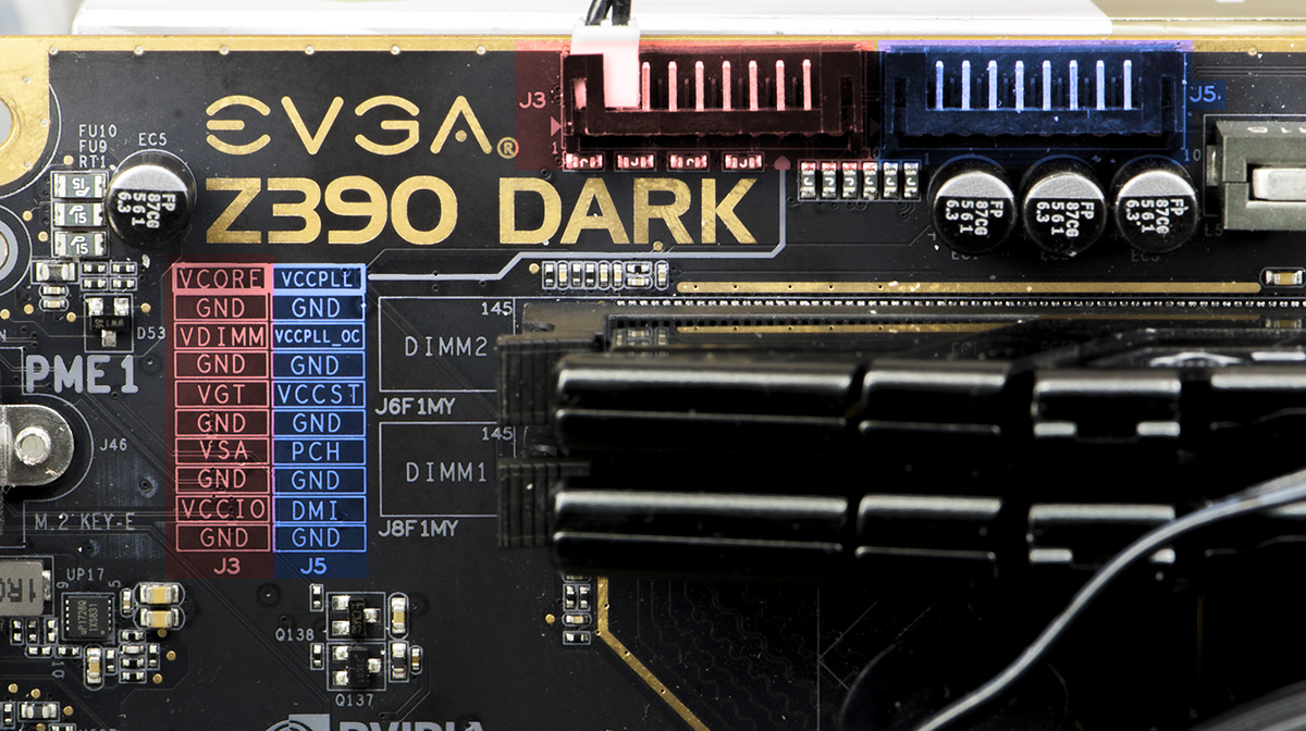
Image 12: ProbeIt connector pinout legend on the PCB silkscreen
All voltage output pins are protected against short circuit, removing risk of damaging CPU or motherboard by accident. ProbeIt adapter to typical DMM banana probe is also shipped with each EVGA Z390 DARK and KINGPIN edition VGA card. If you need to DIY custom cable to connect at EVGA ProbeIt header check these compatible plugs and there pre-crimpled leads.
Labels on Image 12 depict exact pinout of both J3 and J5 ProbeIt connectors, if you want to know signal routing for probe.
Loadline functionality on Z390 DARK VRM
The output capacitors type, quantity and position are important for the good performance of multi-phase VRM. For example, aluminum solid-polymer electrolytic capacitors exhibit large capacitance but the ESR is high compared to an equivalent bank of surface-mount ceramic capacitors. As result load transients that must be sourced by capacitor bank from electrolytic output capacitors will not be handled as well, and output voltage will have a drop due to parasitic ESR and ESL impedances. A typical ESR for a 2200 µF polymer cap is in range 5-10 mΩ. By comparison a bank of 40 × 47 µF X7R multilayer ceramic capacitors will provide similar provides similar capacitance but with just 0.1-0.3 mΩ of ESR and 10 pH of ESL.
Because of high routing density and LGA socket pin count PCB space is often very limited around CPU. To get more space for both high-current power path and DDR4 routing Z390 DARK has increased to 10 number of layers. so signals can be spaced better and not interfere each other as much. A huge amount of effort is put into timing analysis for critical nets. Power and ground are usually run on multiple layers to reduce impedance. Vias need to be in place for connectivity to internal layers without adding impedance. All of these factors make PCB space very expensive. Hence there is always effort to optimize power delivery circuit to meet power and performance criteria, while taking least space possible to allow CPU signals routing and feasible component placement.
One factor to verify during power delivery design is good transient performance. All high-speed chips like CPU or GPU exhibit a certain amount of current leakage through the silicon structures and package. This leakage is always present, even when processor is not doing anything and sitting idle. Some designs and manufacturing technologies exhibit a cubic change in current for an incremental step change in core voltage. Because of this leakage, it is desirable to keep voltage as low as possible, so the total power is reduced and temperatures are improved. Voltage overshoot (voltage increase when processor going from loaded to idle state) is another negative impact for thermals and power. Improving the overshoot characteristics will as result reduce the temperature of the processor and allow more stable operation at desired clock.
On the other end, one cannot simply use minimal voltage level, especially during overclocking. Certain voltage level is required to allow faster transistors switching times and increase clock frequency of the chip. If voltage is too small, transistors will not be able to switch as fast, rendering errors in processor operation. We see effect this as stability issues, calculation errors or even more severe results such as hangs or BSODs.
Knowing about both of these factors allow us to understand why voltage regulation for high-performance processors and graphic chips is very important. VRM must deliver accurate voltage within narrow tolerance from optimal CPU/GPU operation point, while keeping thermal stress and electrical noise minimized. All modern designs also implement adaptive voltage control, using different levels of supply voltage depending on processor workload. If CPU is idle or have low load (like running browser with this article) there is no need for high voltage. To improve thermal processor can command VRM to reduce voltage and drop its clock to lower value to save power. Interoperation between VRM and CPU is part of feature set in SVID protocol, and different VID is preprogrammed into each specific CPU sample during fabrication tests. Unused cores also can be power gated and turned off, allowing further power/thermal improvements, at cost of the increased wake-up latency.
| Conditions | No loadline used | Loadline 1.0 mΩ used |
|---|---|---|
| CPU idle, 5A, 1.00 V | Leakage current, V*I = 5 W | Leakage current, V*I = ~5 W |
| CPU light load, 20A, 1.00 V | Power V*I = 20 W, no Vdroop | Power (V-Vdroop)*I = 19.2 W, Vdroop = 19.61 mV |
| CPU medium load, 50A, 1.00 V | Power V*I = 50 W, no Vdroop | Power (V-Vdroop)*I = 45.4 W, Vdroop = 47.62 mV |
| CPU high load, 150A, 1.00 V | Power V*I = 150 W, no Vdroop | Power (V-Vdroop)*I = 113.4 W, Vdroop = 130.5 mV |
| CPU stress load, 250A, 1.00 V | Power V*I = 250 W, no Vdroop | Power (V-Vdroop)*I = 160 W, Vdroop = 200 mV |
Table 3: Loadline impact illustration on power taken by CPU
Adaptive voltage control is not the only thing that keeps processor cool while delivering all those GFlops. Good VRM design also account for physical design on motherboard and implements loadline function. Transistor in processor need power to switch between states, however once they switched, only power consumed would be static leakage. So we want enough voltage during “switching phase” but less voltage at “idle phase” to reduce leakage power. Sounds simple in theory, but there is a problem here. Because of the high clock frequency we cannot control voltage fast enough to fully meet such power requirement. But we can instead “suggest” to processor’s power controller about VRM capability and board delivery quality by introducing artificial current vs voltage vector. This is commonly referenced as loadline and expressed in milliohms. Loadline defines a negative voltage offset slope with respect of current drawn by a chip. Using loadline allow to reduce voltage on the fly under load at same time while maintaining higher voltage in light/idle conditions. It is a bit counterintuitive concept, but loadline functionality help to reduce Vcore voltage as the CPU loading increase.
Actual loadline settings and voltage drop (Vdroop) effect can be adjusted in Z390 DARK BIOS. There are multiple steps available to fine-tune setting for each particular use case. Be sure to check related section for details and analysis.
But wait, you say, if there is 200mV Vdroop under stress load condition, then CPU receive only 1.00 V – 0.2 V = 0.8 V and get unstable? In reality, it’s not as simple, because CoffeeLake CPU also have own power management control which can request different voltages from VRM controller, when loadline is factored in. BIOS programs loadline into special CPU registers for this. Processor then request different (often higher) voltage from VRM, with loadline effect accounted for. Loadline function is independent of VID control, so those two functions are dynamically working together to adjust Vcore on the fly, depending on CPU clocks, utilization and communication with VRM.
Also all modern CPUs have special voltage sense points, routed independently by kelvin connection from VRM controller to die level so that the die level Vcore voltages are regulated correctly. Because VRM controller feedback is using these special die level sense signal output voltage at the VRM inductors can be set higher than BIOS setting. There is always some loss of voltage across the copper PCB plane, so controller will compensate this, using die sense feedback.
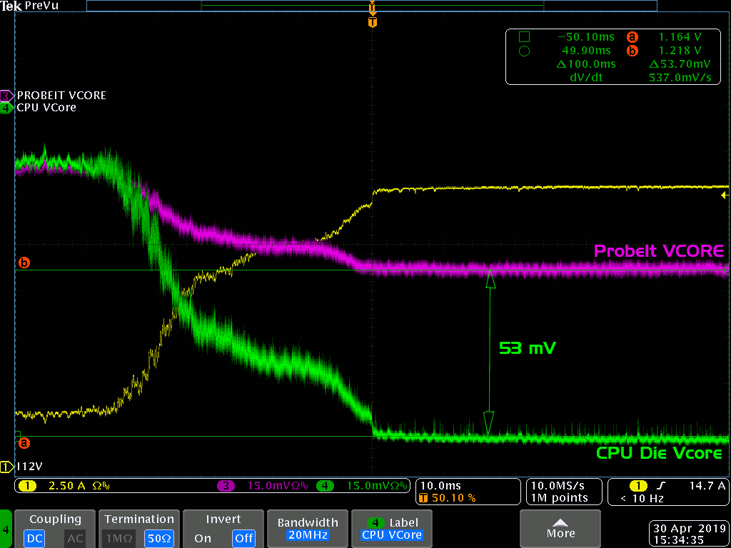
Image 13: Voltage measurement difference from location change (purple at ProbeIt, green at CPU die)
ProbeIt header on the Z390 DARK reads voltage from the CPU socket cavity area, not exactly at the die level. This also result in some readings difference between CPU die Vcore and board readout under load. During Vdroop test I’ve measured difference under load between ProbeIt pins and actual CPU die voltage, which you can see on Image X oscilloscope screenshot.
Intel specification for Vcore tolerance (TOBVCC on page 118) is ±20mV at the die level. This is what motherboard is designed to maintain at default Loadline Vdroop settings. If you use DMM that will read only average value, then voltage from Socket (routed to ProbeIt connector) is relaxed to ±5% variation, depends on Loadline and actual load on CPU.
Loadline effect can be also completely disabled, resulting in worst possible condition for processor operation in respect of power/temperatures. This is why disabling loadline is really only available as an option for extreme overclocking with sub-zero temperatures, otherwise CPU will overheat with any serious overclocking even with watercooling.
LED Diagnostic indicators
Board also have indicators for real-time voltage health check. All important voltages have dedicated white LED to show power presence on related rail. Eight LEDs grouped in line near BIOS update USB port and power/reset buttons in top right corner of the motherboard, just above the 24-pin ATX power connector. In normal operation all white LEDs should be light up, meaning all voltages are present.
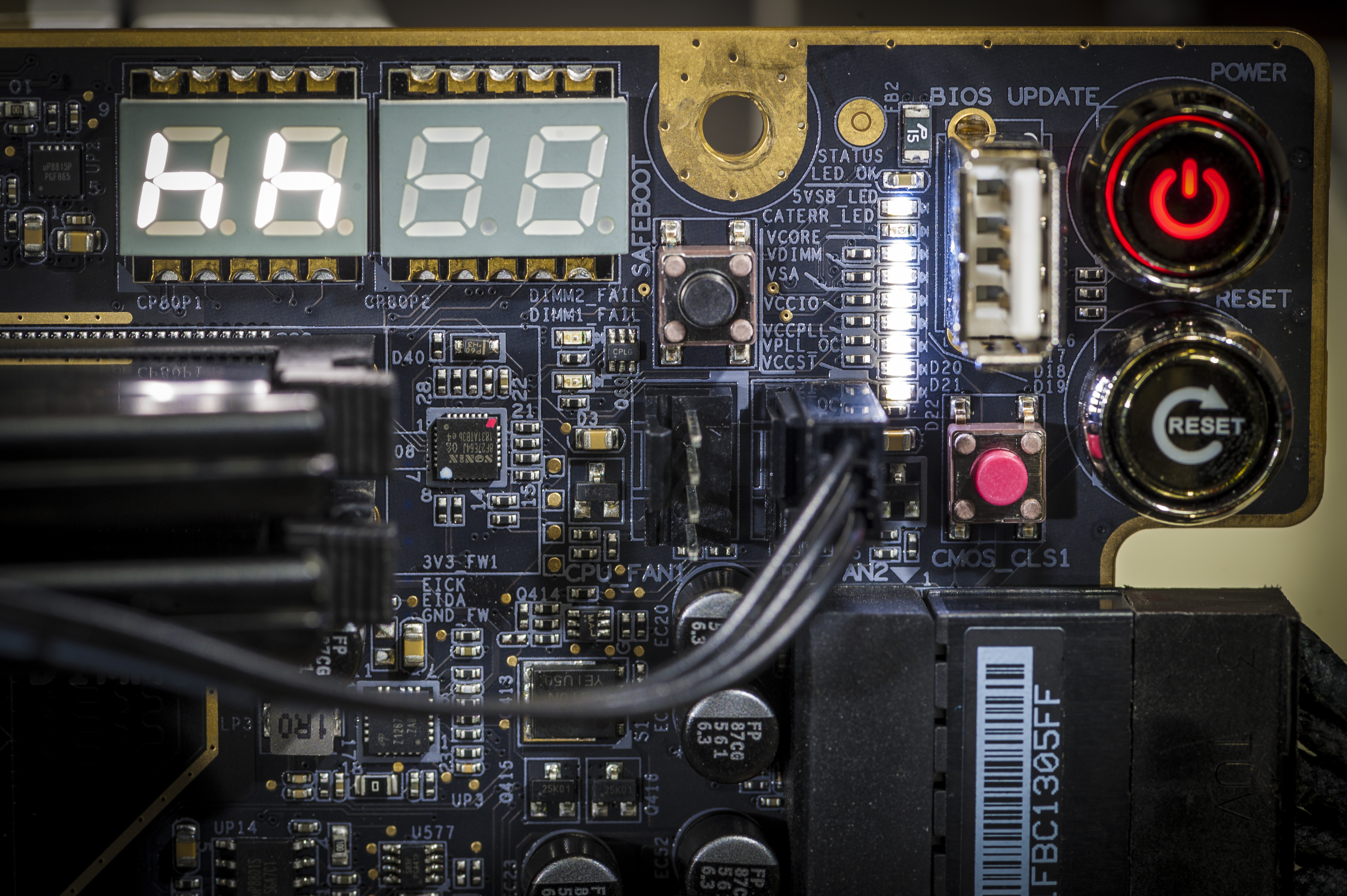
Image 14: Diagnostic LED indicators for voltage status and errors
To confuse unprepared user I’ve put one red LED in the mix, second from the top. This is CATERR_LED, to indicate CPU Catastrophic Error condition. If you ever see this red LED to come on, it means CPU failed to run desired settings/clocks, you got cold-bug in extreme overclocking session or CPU/board are simply faulty. There are also two red LEDs between DIMM slot latches and SAFEBOOT button, to indicate memory training failure. DIMM1_FAIL LED is bottom one, showing that CPU having issues to train memory installed in slot DIMM1. DIMM2_FAIL LED does the same thing for far DIMM2 slot. In normal operation these should be off.
| LED location (from top right motherboard corner) | Color, normal state | Purpose |
|---|---|---|
| Top, +5V Stand-by | White, always on | Display presence of +5V Standby from PSU |
| 2nd, CATERR_LED | Red, normally off | Indicates CPU Catastrophic error, CPU hung/crashed |
| 3rd, VCORE Voltage | White, on at power on | VCORE Voltage present |
| 4th, VDIMM Voltage | White, on at power on | VDIMM Voltage present |
| 5th, VSA Voltage | White, on at power on | VSA Voltage present |
| 6th, VCCIO Voltage | White, on at power on | VCCIO Voltage present |
| 7th, VCCPLL Voltage | White, on at power on | VCCPLL Voltage present |
| 8th, VCCPLL_OC Voltage | White, on at power on | VCCPLL_OC Voltage present |
| Bottom, VCCST Voltage | White, on at power on | VCCST Voltage present |
Table 4: LED definition for status indication
VCORE LED in Adaptive Mode or without overclocking might be flickering or very dim, due to CPU Vcore power management operation. To save energy CPU Vcore can go to a low voltage state, dimming or even turning LED off. That is normal for not overclocked systems and not a reason to get alarmed.1
PCIe device mapping
Due to 16 available PCIe lanes from CPU on LGA115X platforms Z390 DARK provide less PCIe expansion options than X299 DARK flagship.
All CPU lanes are allocated to mechanical x16 PCIe slots, exclusively.
| Configuration | PE1 slot width | PE2 slot width | PE4 slot width |
|---|---|---|---|
| Single x16 device | x16 Gen3 CPU | Empty slot | Empty slot |
| Dual x8 devices, SLI | x8 Gen3 CPU | x8 Gen3 CPU | Empty slot |
| Triple devices | x8 Gen3 CPU | x4 Gen3 CPU | x4 Gen3 CPU |
| VGA card + x4 AIC SSD | x8 Gen3 CPU | Not used | x4 PCIe CPU SSD |
| VGA card + x8 AIC SSD | x8 Gen3 CPU | x8 Gen3 CPU SSD | Empty slot |
| Single x8 device | Not used | x8 Gen3 CPU | Empty slot |
| Single x4 device | Not used | x8 Gen3 CPU | x4 Gen3 CPU |
Table 5: CPU PCIe lanes mapping to x16 mechanical slots
All CoffeeLake CPUs provide 16 PCIe lanes with speed up to Gen3 (8 GT/s). Connectivity and PCIe width configurations are exactly same for any supported LGA1151 Core 8-series and 9-series CPU.
M.2 SSD slots and smaller x4 PCIe slot PE3 are connected to Z390 PCH, thru switches. Their configuration covered in next section.
M.2 slots and NVMe support
State of the art storage today exclusively use NVM Express interface over the PCIe. Solid state drives like Samsung 970 Pro or Intel Optane 905P. All these are fully supported on Z390 DARK M.2 or U.2 ports.
| PCH PCIe configurations | Active port 1 | Active port 2 | Unused deactivated ports |
|---|---|---|---|
| 2 x M.2 SSD device | PM1 from PCH | PM2 from PCH | PU1 U.2, PE3 slot |
| 1 x M.2 SSD + 1 x U.2 SSD | PU1 from PCH | PM2 from PCH | PM1 M.2, PE3 slot |
| 1 x M.2 SSD + x4 PCIe slot | PM1 from PCH | PE3 slot,PCH | PU1 U.2, PM2 M.2 |
| 1 x U.2 SSD + x4 PCIe slot | PU1 from PCH | PE3 slot,PCH | PM1 M.2, PM2 M.2 |
Table 6: PCH PCIe lanes mapping for SSD options
PCIe PE3 ×4 slot have open slot on the inner side, allowing use of full-size PCIe devices with x8 or x16 width. However only x4 lanes are available to device and it will be operating at degraded link speed.
Image 15: PCH heatsink surrounded by NVMe connectivity ports
Rest of the onboard devices are completely independent and can be used at any time without limitations. All SATA ports are always active, there is no switching of SATA ports with PCIe lanes. Also Z390 DARK does not use enterprise version of Intel RSTe, unlike X299 platform there are no VROC keys licensing required to get M.2 SSD RAID working.
Z390 DARK does NOT support SATA M.2 drives on either M.2 slots. Installing one will not damage anything, however drive will not function either.
Onboard controllers
Z390 DARK comes with Creative DSP audio solution, isolated from digital noise by own quiet ground plane and separate power regulators. Line audio output is also amplified for headphones operation.
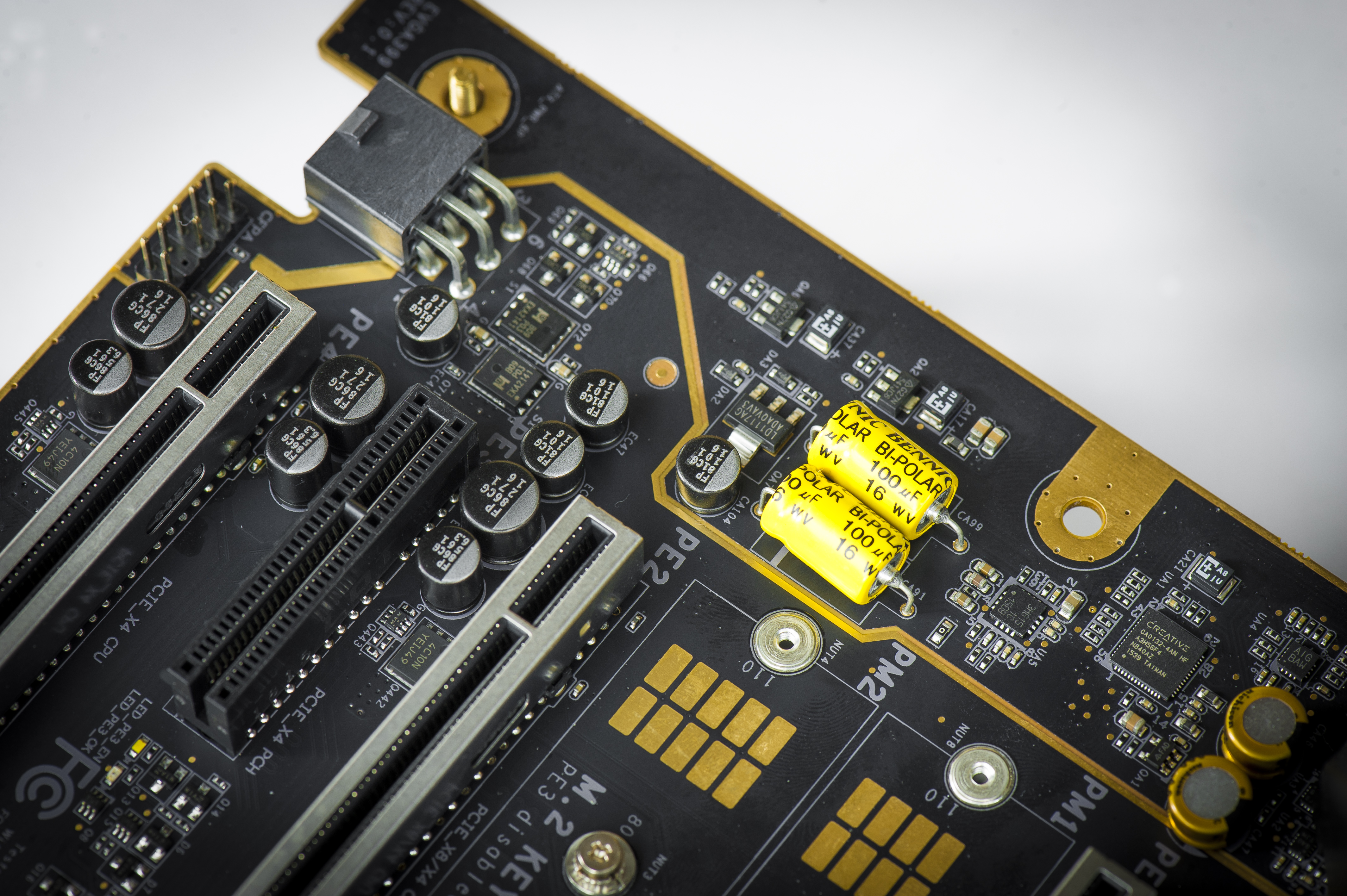
Image 16: Creative audio DSP on isolated PCB zone
Rear USB3.1 Gen2 interface served by ASMedia ASM3142 XHCI controller. This controller handle rear I/O Type-C and red Type-A USB SuperSpeed connectors. There is no PD(Power Delivery) support on these ports. Drivers for ASM3142 are supplied for Windows 7/8/8.1/10 and various Linux distributives.
DARK comes with preinstalled WiFi / BlueTooth 5.0 wireless module. This module is installed in shielded assembly at the rear I/O port, just next to Clear CMOS button. Module is based on Intel® Wireless-AC 9260 interface M.2 2230 Type-E card. It supports 2×2 RF front-end, works on two bands 2.4 and 5.0 GHz to deliver speeds up to 1.73 Gbps with 802.11ac WiFi. Official drivers from Intel support only Windows 10 and Linux.
Fan/pump headers
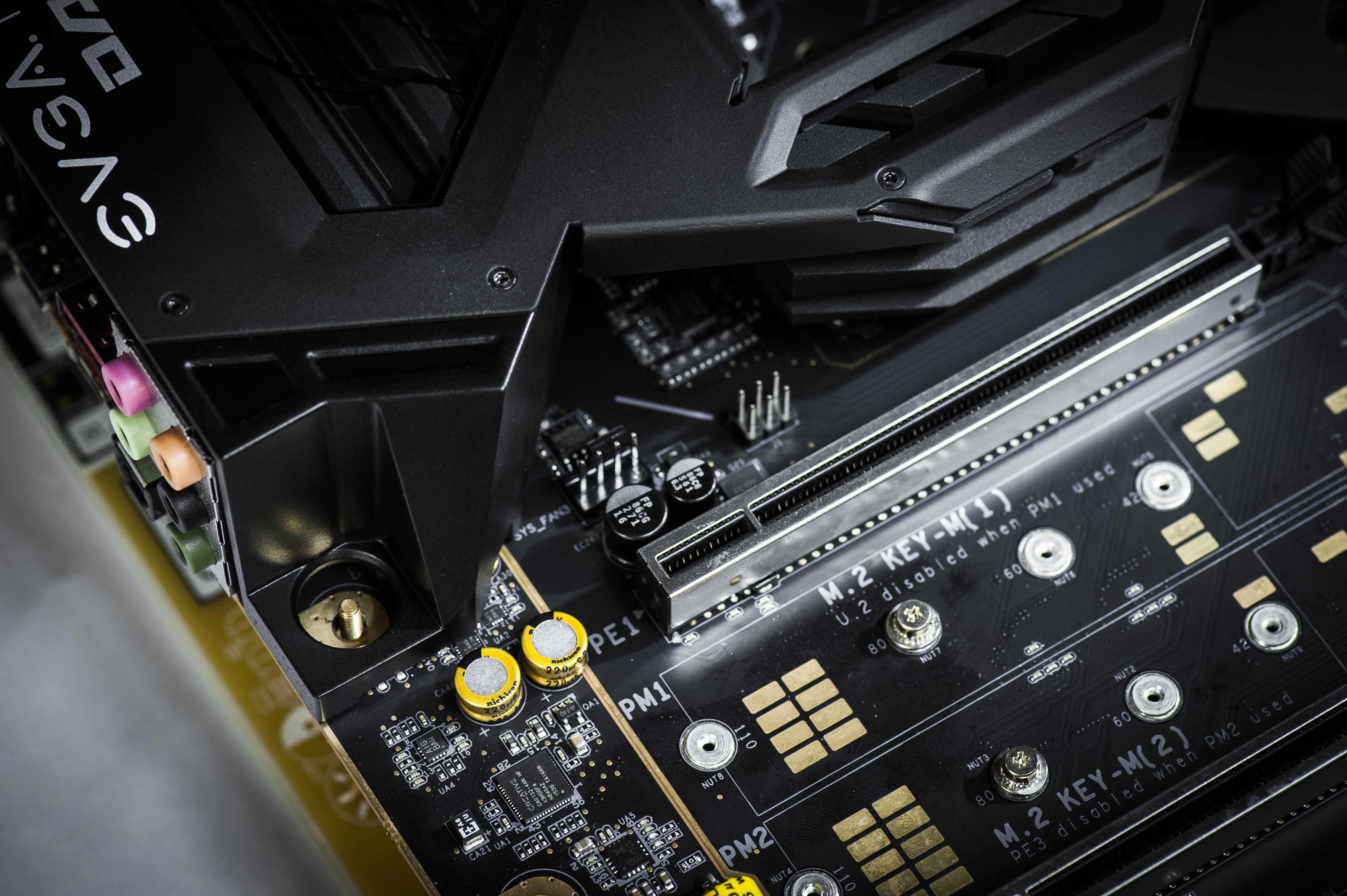
Image 17: First PCIe slot and hidden 4-pin fan header
Individual USB protection
Each USB interface port on Z390 DARK is independently powered. This allow better fail-safe operation, without loosing important USB devices if rogue USB device that is faulty and may draw too much power is plugged in. USB 3.1 Gen2 header for front panel USB Type-C port also provide PD support for charging and DUT power delivery. This can be handy for VR HMD device operation or external storage device like SSD bays.
There are total 15 USB ports of various speed grades and type present on the Z390 DARK. Dedicated USB Type-A vertical connector located near the power buttons designed for BIOS Update function.
Right-angle connectors
Right angled 24-pin connectors were first introduced to consumer motherboard market by EVGA in 2011 (P67 FTW and SLI boards). Same cutout approach for cable clearance is used for bottom corner 6-pin PCIe power connector. This connector mates with standard 6-pin ATX VGA power cable, to provide an additional power source for PCIe slot +12V power, in case of using dual-GPU cards, such as legacy dual-GPU GeForce GTX x90 monsters.
Two right angle USB 2.0 headers located on the bottom edge under chipset provide four legacy ports, with help of USB2.0 bridge controller.
Multifunction 80Port LED display
Yet another video from Gamers Nexus also covers most of features above in video format:
Software for Z390 DARK overclocking
Intel Extreme Tuning Utility is a good tool to adjust various settings such as CPU ratio, ring ratio, various power settings for Z390 DARK board.
BIOS & Tools
EVGA Z390 DARK Special XOC/XP BIOS
ASMedia SATA driver for XP
ASMedia USB Host driver for XP
USB system driver for XP
Installation guide for Windows XP on Z390 DARK
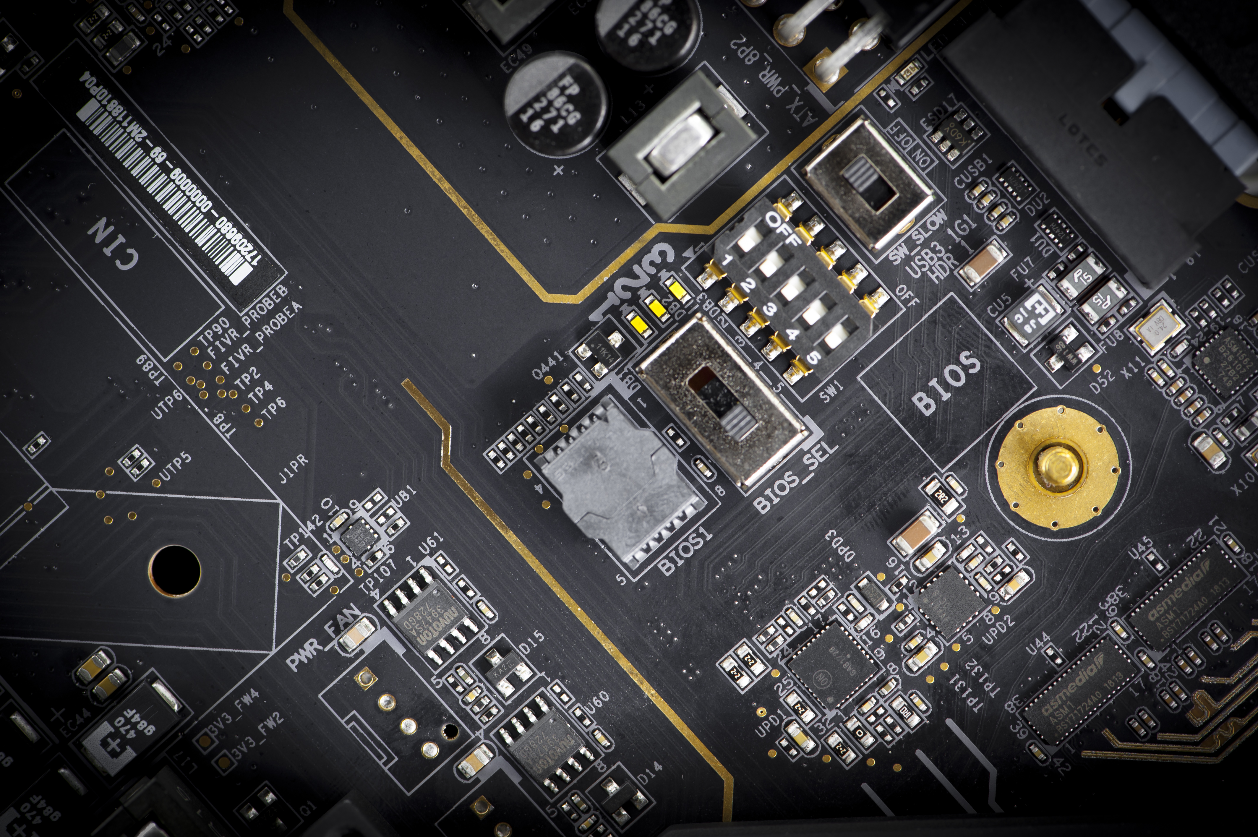
Image 18: BIOS switch selector and socketed BIOS1 ROM chip
If your board have old BIOS version before version 1.04, please update BIOS to 1.04 or later. Otherwise controls/settings discussed below not apply directly.
EVGA Z390 DARK BIOS, Version 1.06 Mirror
EVGA Z390 DARK BIOS, Version 1.04 Mirror
Optimal BIOS Installation procedure:
- Extract the contents of .zip file to USB flash drive (must be formatted as FAT32)
- Reboot the machine and boot into the system BIOS setup menu
- From the BIOS, navigate to the Save & Exit tab and open Select BIOS File
- Select the .bin file you wish to flash. Do not turn off or reset the system during the process, it will reboot itself automatically.
BIOS overview and control items detail
Please note, if you have saved settings into profiles, they will be erased/lost during BIOS update procedure.
Overclocking tricks and settings in BIOS
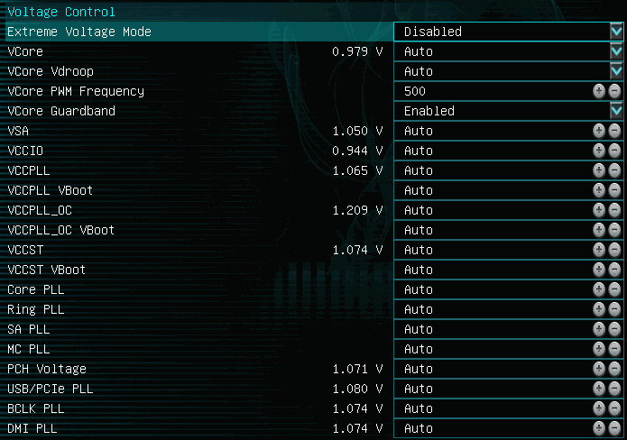
Image 19: Voltage settings in BIOS setup
| Setting name in BIOS | Range (XOC mode) | Notes | Default setting |
|---|---|---|---|
| Extreme Voltage Mode | Enabled or Disabled | Unlock high voltages for extreme overclocking | Disabled |
| Vcore | Auto, Adaptive or Override | Main Core voltage, recommended below 1.4V for 24/7 | VID, 0.8 to 1.3 V |
| Vcore Vdroop | Auto and 9 settings | Loadline and Vdroop settings | Default 0% setting |
| Vcore PWM Frequency | Auto, 400 – 800 kHz | Switching frequency for Vcore PWM | 500 kHz |
| Vcore Guardband | Enabled / Disabled | Keep this Enabled to meet Intel VRM specs | Enabled |
| VSA | Auto, 0.80 – 1.55 V (1.65 V) | System Agent. Impact memory controller OC together with VCCIO | 1.05 V |
| VCCIO | Auto, 0.95 – 1.55 V (1.65 V) | I/O voltage. Impact memory stability and cold-bug | 0.95 V |
| VCCPLL | Auto, 1.00 – 1.4 V (2.5 V) | Runtime VCCPLL | 1.05 V |
| VCCPLL Vboot | Auto, 1.00 – 1.4 V (2.5 V) | Initial power-on voltage for VCCPLL | 1.05 V |
| VCCPLL_OC | Auto, 1.20 – 1.4 V (2.4 V) | Runtime VCCPLL | 1.20 V |
| VCCPLL_OC Vboot | Auto, 1.20 – 1.4 V (2.4 V) | Initial power-on voltage for VCCPLL | 1.20 V |
| VCCST | Auto, 1.00 – 1.2 V (1.55 V) | Runtime VCCPLL | 1.05 V |
| VCCST Vboot | Auto, 1.00 – 1.2 V (1.55 V) | Initial power-on voltage for VCCPLL | 1.05 V |
| Ring PLL | Auto, 0.90 – 1.4 V (1.845 V) | Ringbus PLL rail, may affect Ring OC | Auto |
| SA PLL | Auto, 0.90 – 1.4 V (1.845 V) | System agent PLL | Auto |
| MC PLL | Auto, 0.90 – 1.4 V (1.845 V) | Memory controller PLL | Auto |
| USB/PCIe PLL | Auto, 0.90 – 1.4 V (2.00 V) | High-speed interfaces PLL | Auto |
| BCLK PLL | Auto, 0.90 – 1.4 V (2.00 V) | BCLK PLL, can help to push high/low BCLKs | Auto |
| DMI PLL | Auto, 0.90 – 1.4 V (2.00 V) | DMI PLL, can help with 3D benchmarking at high OC | Auto |
| PCH Voltage | Auto, 0.90 – 1.2 V (1.70 V) | Z390 PCH logic voltage | 1.05 V |
Table 7: Voltage ranges and settings
Unlike rest of the system voltages CPU Vcore can be programmed in two modes, as Adaptive Mode or Override Mode. Same as previous LGA115X Intel processors adaptive mode set the voltage depends on frequency that user want to run when CPU under load, while keeping lower voltage under idle or low-load conditions. Adaptive mode is Intel’s default operation. If CPU is overclocked above the Turbo maximum ratio algorithm in CPU power management controller will calculate voltage increase based on running frequency V/F curve and entered target voltage. Offset setting allow further finetune to shift V/F curve point to obtain higher or lower voltage. Voltage range for Adaptive mode is 0.80 to 1.50 V (or 1.72 V in XOC mode). Offset range for Adaptive is -500 to +300 mV (+500 mV in XOC mode). This mode provides best thermals while keeping voltage control, especially if system cooled by traditional fansink.
Vcore Override Mode does the opposite and forces fixed static target voltage. CPU will get constant voltage under all conditions, even when sitting idle. This cause significant thermal stress on the chip and not recommended to use other than for benchmarking and overclocking.
VCCPLL, VCCPLL_OC and VCCST have two different setting values, called as runtime value (normal item) and boot-up value (Vboot). Many CoffeeLake processors cannot boot with very high voltage required for cold-bug free operation, so you need to set lower Vboot voltage to allow processor booting and increase voltage to higher level once initialization is completed.
PLL is a internal circuit block inside CPU that handle clock generation. There are many clocks inside the chip that have different origin sources and drive different parts inside the package. It is important to keep voltage that feeds PLL clean and properly leveled, because any voltage instability will directly impact output clock performance. Higher PLL voltages can shift operation “window” allowing for higher stable overclocks. Also if PLL voltage is too high minimum clock might get too high and CPU will stop working. Each domain have own PLL voltage source to isolate noise and interference, so this is a reason why you see so many different independent PLL settings on Z390 DARK. Depends on your overclocking needs some of PLLs may need adjustment, while other settings can be left alone on default or near default settings.
Usually good rule of thumb is to use around 1.20 … 1.35 V on VCCIO and VSA rails. These voltage levels provide enough margin to maximize memory overclocking for common CoffeeLake CPU. For 24/7 daily use optimal to use 1.25 V or below, given this is enough for desired memory and CPU clocks. If you having stability issues DDR4 overclocking, worth to try various settings, in range from 1.15 to 1.35 V to isolate bottleneck. Some CPUs and memory configurations actually may become unstable when VCCSA voltage is over 1.30 V, so testing both of these voltage might take some time to reach a sweetspot. Memory voltage is also important factor to the system stability. Because this finetuning is dependent on particular CPU sample and memory used we cannot give one set of settings that will work for every case. It’s bit of a process here.
Vdroop setting and it’s impact on CPU operation
Now time to talk more about available loadline settings. In EVGA BIOS these are available as VCore Vdroop control on OC page. There are 9 available settings. Auto is same as Default, which is stock configuration. These vdroop settings derived directly from different loadline slope adjustments available from digital Intersil controller. Vdroop control affects Vcore voltage regulation in both Adaptive and Override mode settings.
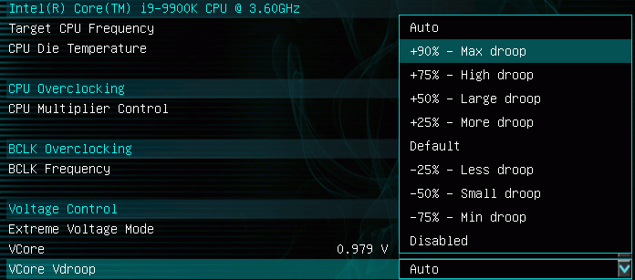
Image 20: VCore Loadline settings in Z390 DARK BIOS
Different levels have huge impact on platform power and thermals. Loadline and vdroop settings often misunderstood as “small finetune” setting, but impact is actually very significant. To capture real-world data from actual system, I’ve prepared a test rig to capture some voltage and current waveforms.
| Motherboard | EVGA Z390 DARK |
| Processor | Intel® Core™ i9-9900K, 5 GHz, stock clocks |
| BIOS used | Z390 DARK version 1.06 release version |
| CPU Voltage | 1.250 V fixed, Override mode. Everything else Default/Auto |
| Fan speeds | 100% on simple CPU aluminum heatsink |
| DRAM | 2 x G.SKILL F4-3600C16D-16GVK |
| Storage | Intel 760p 256GB |
| Graphics card | Retail EVGA RTX 2080 Ti KPE, Hybrid cooler |
| PSU | EVGA NEX 1500W Classified |
| Benchmark | Intel AVX1 stress test tool |
| Oscilloscope | Tektronix MDO4054C |
| Current probe | Tektronix TCPA300 + TCP303, rated up to 150 A, 15 MHz |
| Voltage probe | Tektronix P6251 and P6246 Differential probes, rated up to ±42 V, 1 GHz |
Table 8: Vdroop analysis demo system specification
Using oscilloscope for these test allow us to detect and analyze both fast peak and average settled power and voltage levels. Measuring with usual TrueRMS DMM will give only averaged values and will not really show true picture in this case.
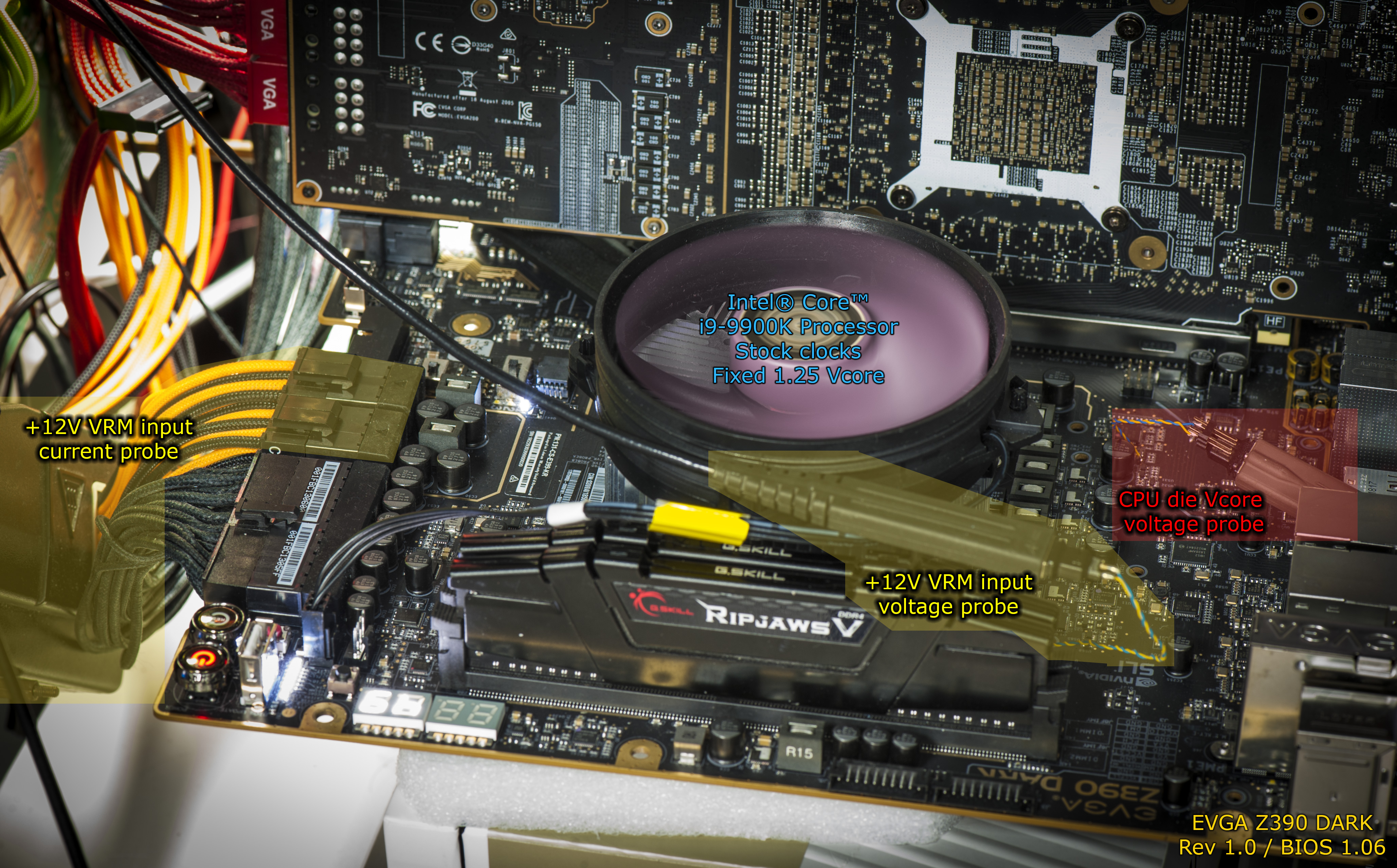
Image 21-22: Test motherboard rig with Vdroop test probes attached
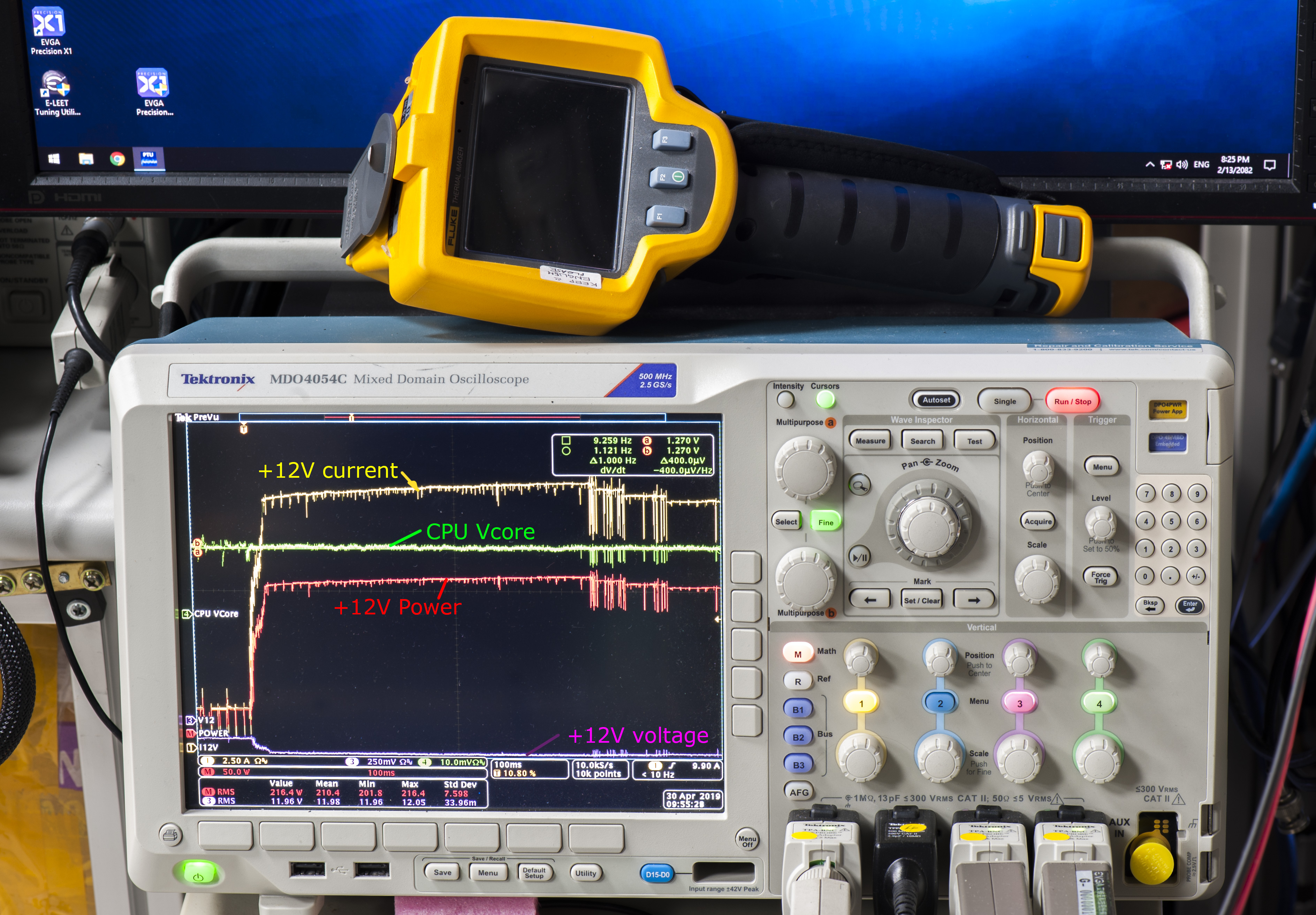
Image 23-24: Measurement scope used for Vdroop test
Vdroop test method is to apply Vdroop setting in BIOS, boot OS, run the stress test, capture two screenshots with idle to load voltage transition to analyze power and voltage delivered to processor. Then repeat same test procedure for all the rest of the Vdroop settings in BIOS. During all test runs +12V current and +12V voltage delivered to VRM was also measured. Power delivered to processor’s VRM in watts is calculated as PVRM = measured +12V voltage × +12V current. This power reading combine both CPU power and VRM power, including all power loss during conversion 12V to Vcore/VSA/VCCIO. Power taken by VSA and VCCIO considered constant during tests, as we only test difference between different CPU VCore Vdroop settings.
Captured screenshots for each of the test setting also presented below on Image X-X. Each screenshot have horizontal cursors and legend showing measured +12V power and CPU Vdroop. These might look just like a bunch of colorful nonsense lines but there is actual meaning to all this. Each graph is 2D representation of voltage/current measured over time interval. Vertical is amplitude of the signal. Higher the line point is – the higher the voltage measured. All graphs start at Windows idle condition, then AVX1 stress test started and change from idle state to fully 100% loaded state is captured.
- Green line is CPU die VCore voltage signal.
- Yellow line is +12V current from PSU.
- Purple line (visible on the bottom of the chart) is +12V voltage from PSU.
- Red line is calculated +12V power delivered to CPU and VRM.
You see lot of noise and jumping around when CPU transition from idle state to loaded state. CPU and motherboard are complex devices, and they don’t turn on or off like a simple bulb lamp. It takes short time to load the application data into memory, then into CPU cores cache and finally ramp up all cores running math. During this process we see voltage and power change, and that is why lines wiggle much between idle and loaded condition. Each screenshot is clickable to see non-resized high-quality version.
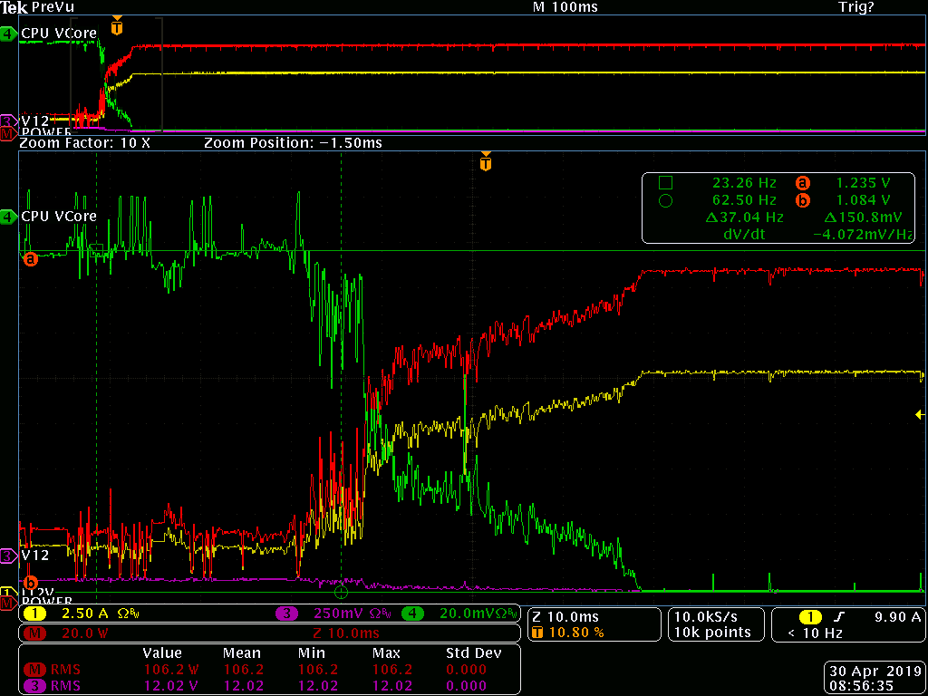
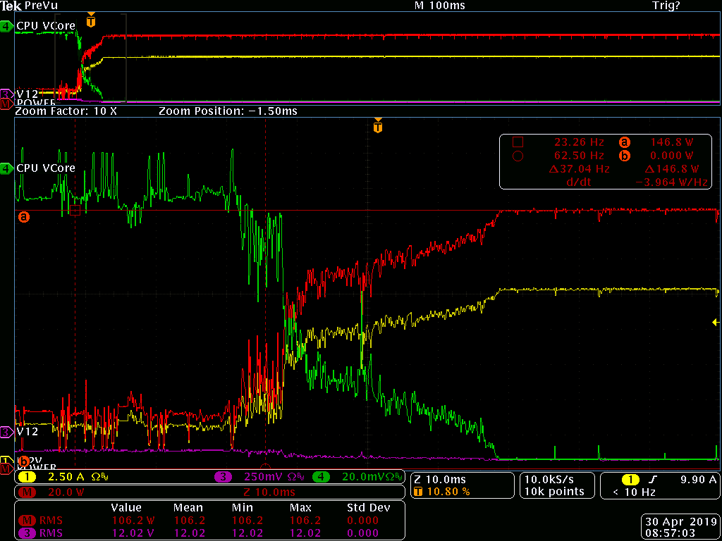
Image 25-26: BIOS Vdroop setting +90 %, Vcore drops 151 mV.
Left graph is showing measured Vcore voltage (green chart), with cursor lines (thin horizontal line on top (idle state) and bottom (loaded state). Cursor legend on right top corner displays useful information, like a cursor value, b cursor value. Vdroop is already calculated for us, as Δ 150.8 mV in case of +90 % Vdroop setting. Horizontal time span on these screenshots is 100 ms (that is 0.1 seconds).
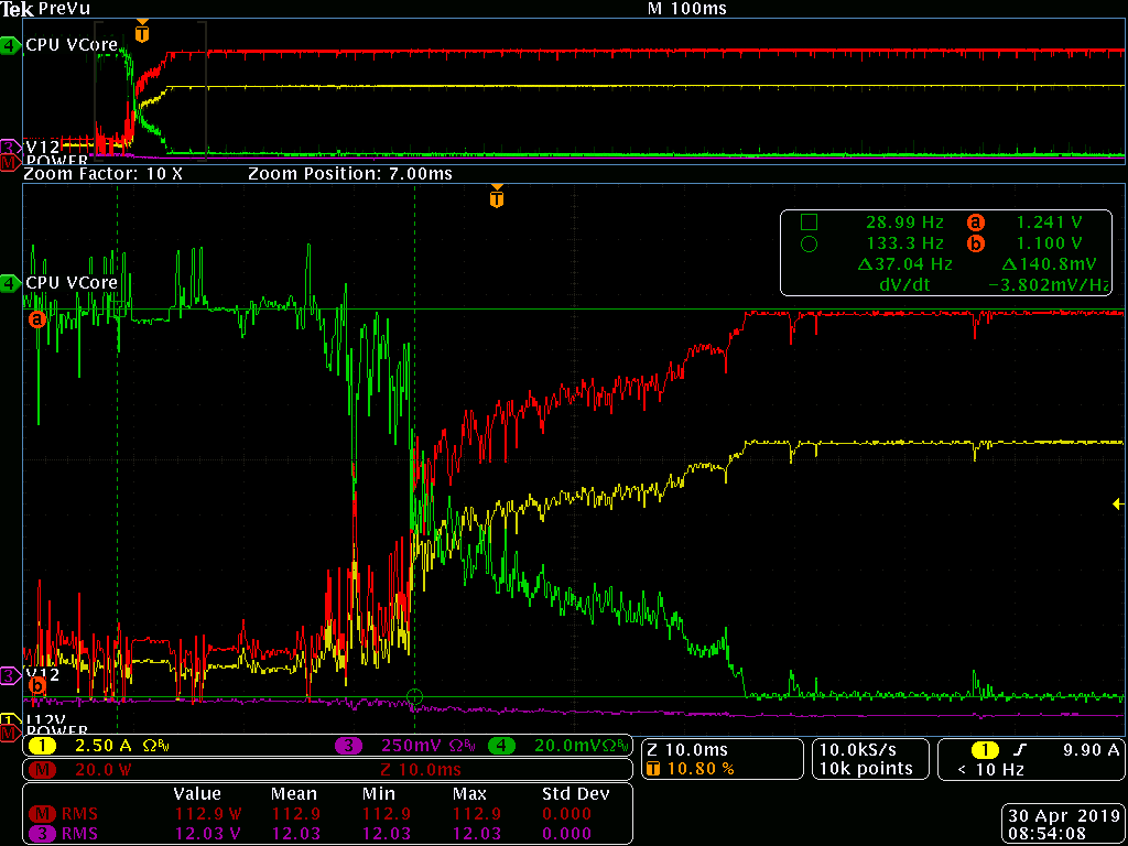
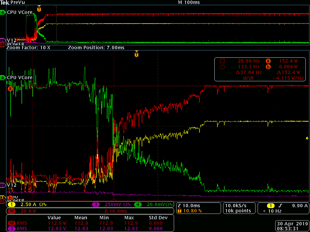
Image 27-28: BIOS Vdroop setting +75 %, Vcore drops 141 mV.
Right graph is same waveform, but this time cursors display measured +12V power, with red cursor lines (thin horizontal line on top (idle state) and bottom (loaded state). Cursor legend on right top corner displays power. B cursor is set to zero power, so power is directly calculated as Δ152.4 W in case of +75 % Vdroop setting. Rest of the charts follow very same format.
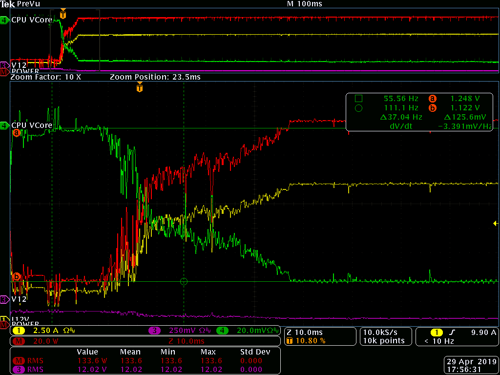
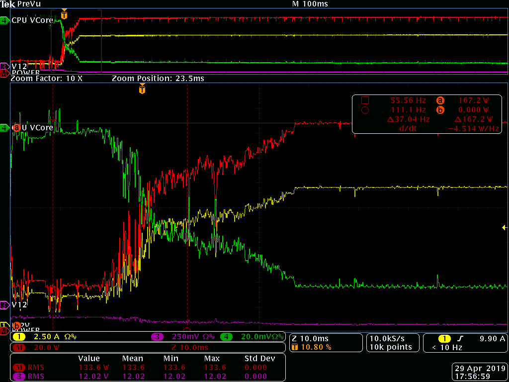
Image 29-30: BIOS Vdroop setting +50 %, Vcore drops 126 mV.
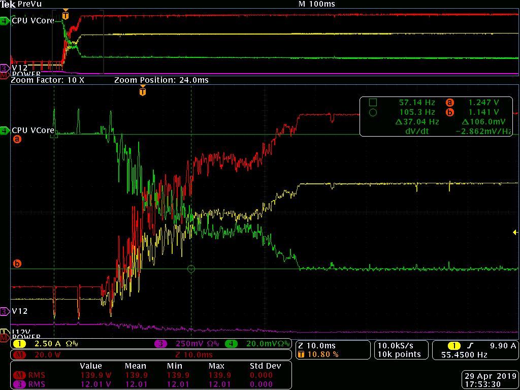
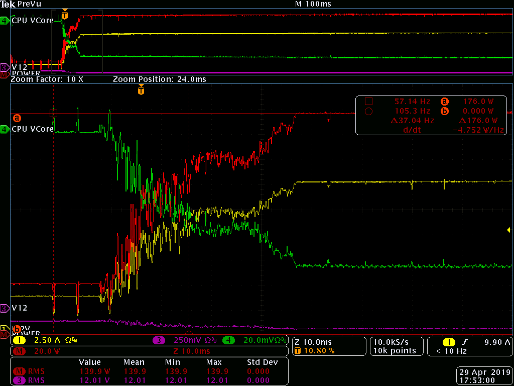
Image 31-32: BIOS Vdroop setting +25 %, Vcore drops 106 mV.
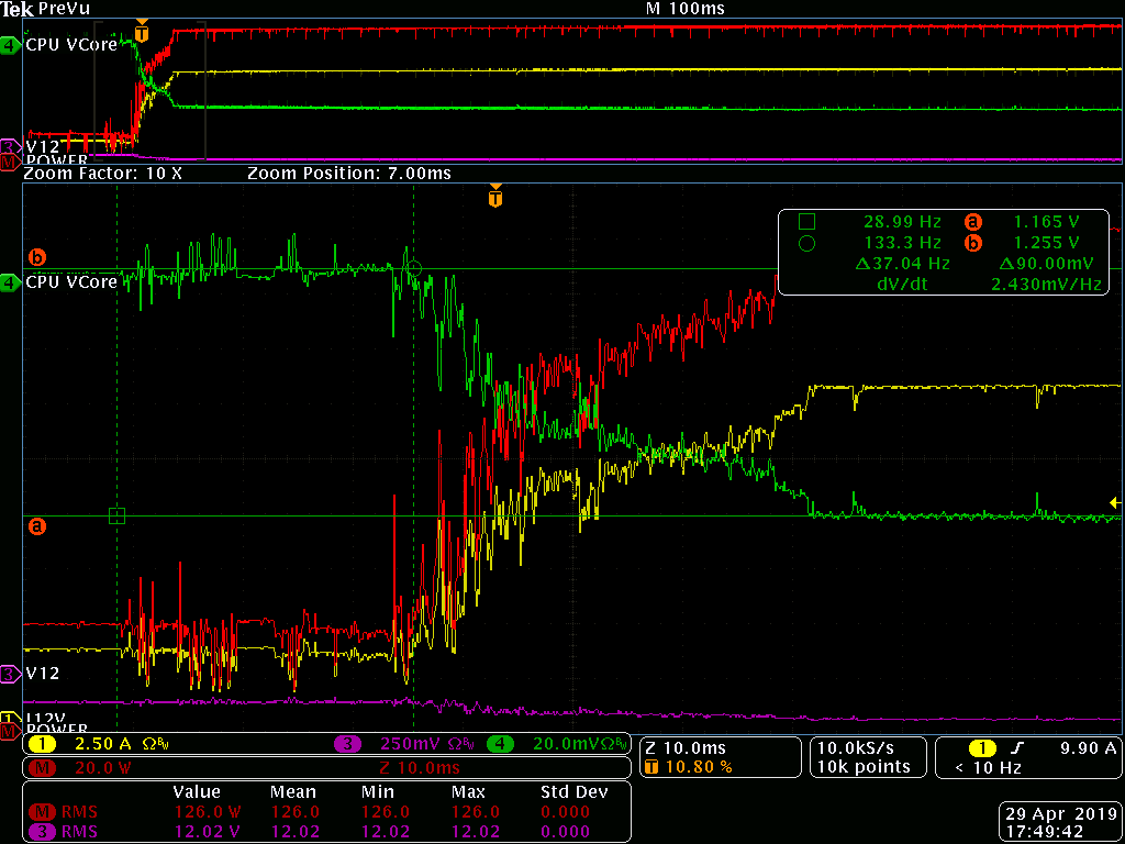
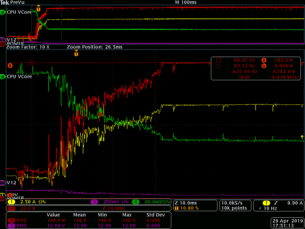
Image 33-34: BIOS Vdroop setting at default level (same as Auto), Vcore drops 90 mV.
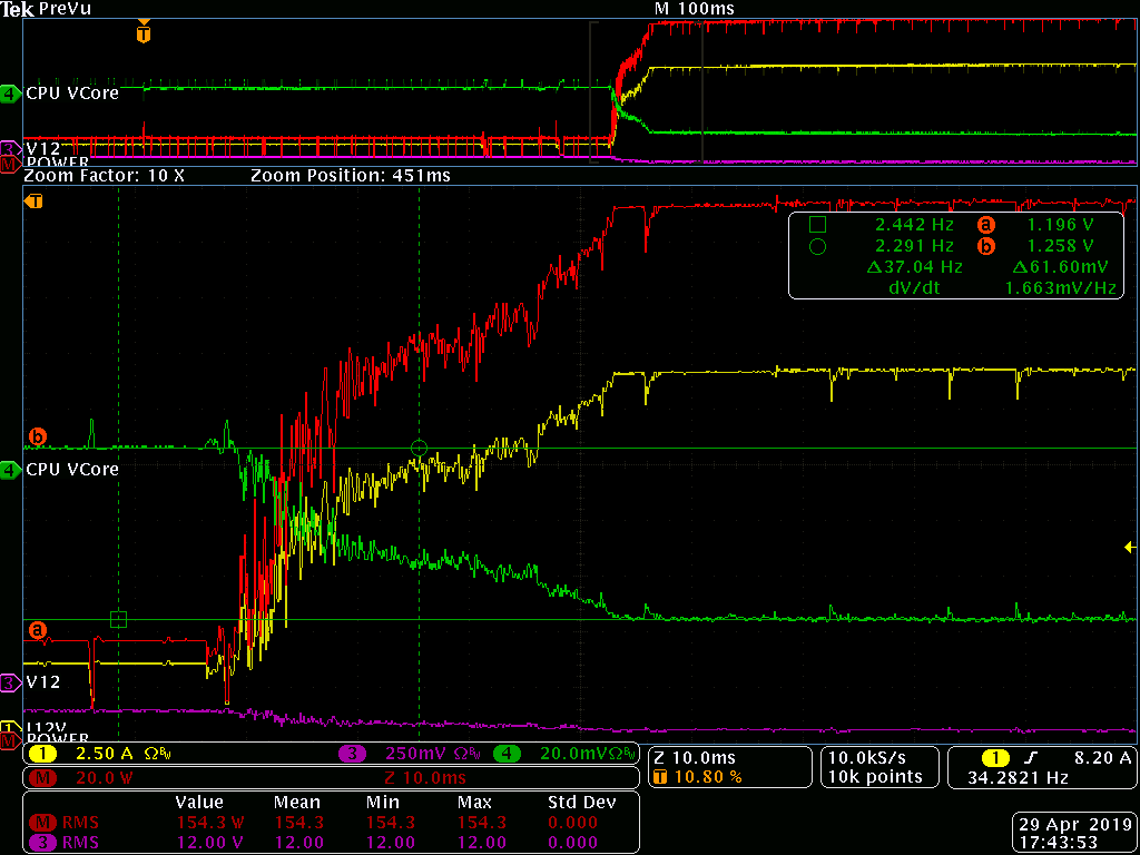
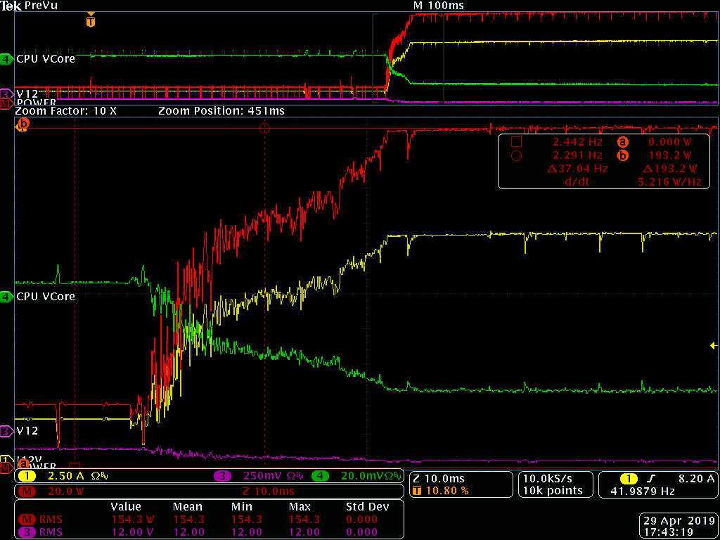
Image 35-36: BIOS Vdroop setting -25 %, Vcore drops 62 mV.
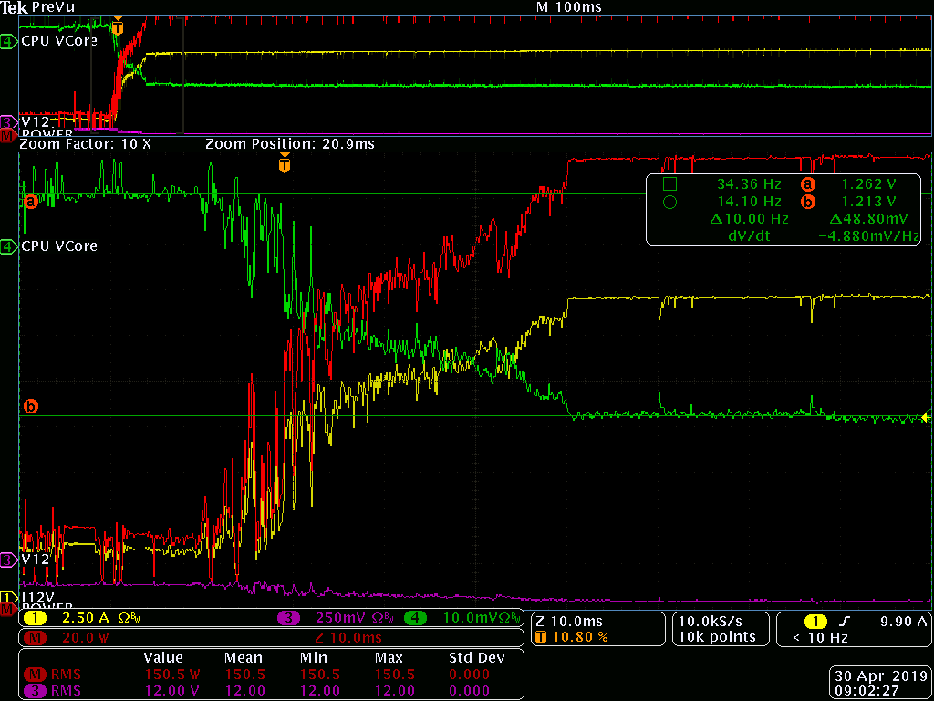
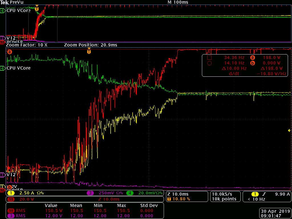
Image 37-38: BIOS Vdroop setting -50 %, Vcore drops 49 mV.
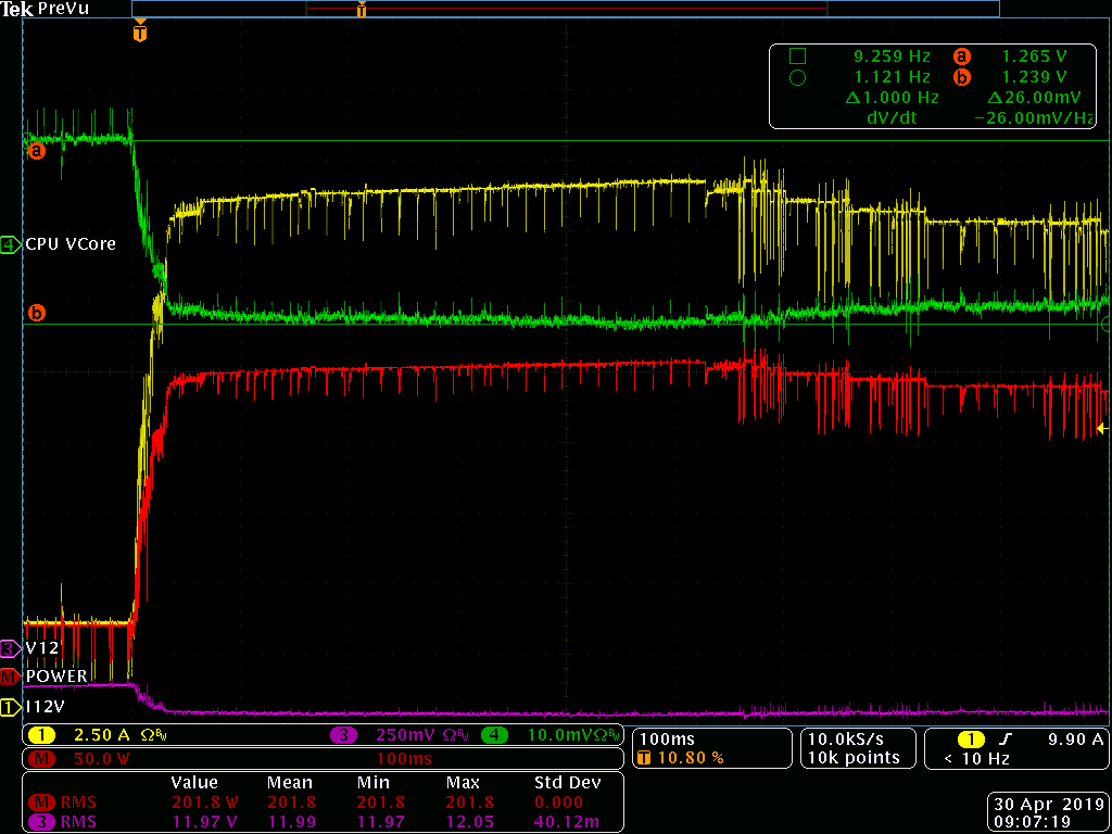
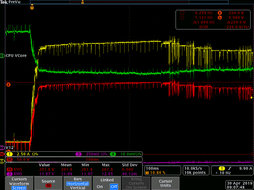
Image 39-40: BIOS Vdroop setting -75 %, Vcore drops 26 mV.
This chart shows complete waveform with full 1 second of captured data. Here we can see what happens when CPU overheats, by clear indication on reduction of current and power in the right side of the chart. It took only 0.6 seconds to hit critical temperatures and CPU started to throttle, skipping clocks to avoid further temperature rise.
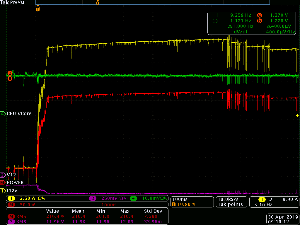
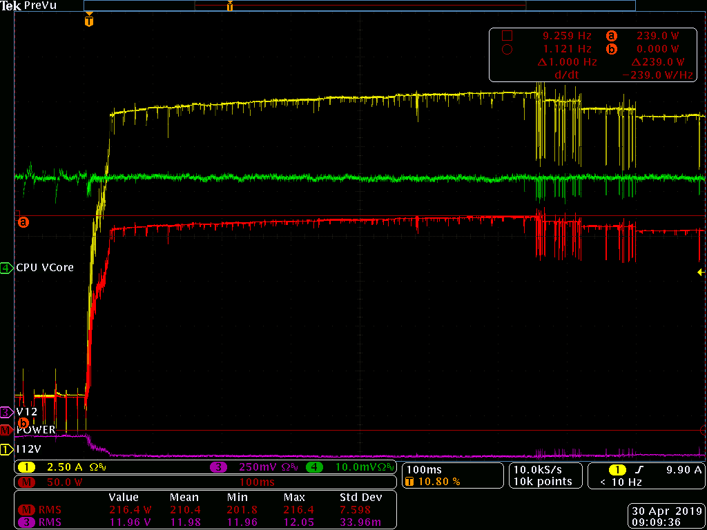
Image 41-42: BIOS Vdroop setting disabled, Vcore stays constant
Image 43 provides simplified summary graph with all these tested points, with relation to each CPU Vdroop setting.
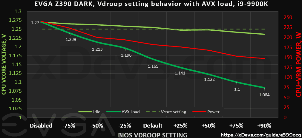
Image 43: Loadline droop summary graph
Reminder – these values are with forced 1.250 V override Vcore setting. Default CPU voltage is governed by power-management and VID, so actual voltage at default is not what shown on the chart.
Same data also in table legend format, showing each point details.
| Vcore Setting and Vdroop | CPU Voltage, idle | AVX1 load | CPU Temperature, loaded | CPU+VRM Power combined |
|---|---|---|---|---|
| Override 1.25V, +90% – Max droop | 1.235 V ±25 mV | 1.084 V ±25 mV | +76 °C (before crash) | 147 W |
| Override 1.25V, +75% – High droop | 1.241 V ±25 mV | 1.100 V ±25 mV | +86 °C | 153 W |
| Override 1.25V, +50% – Large droop | 1.248 V ±25 mV | 1.122 V ±25 mV | +89 °C | 168 W |
| Override 1.25V, +25% – More droop | 1.247 V ±25 mV | 1.141 V ±25 mV | +94 °C (throttle) | 176 W |
| Override 1.25V, Default (Auto) | 1.255 V ±25 mV | 1.165 V ±25 mV | +98 °C (throttle) | 182 W |
| Override 1.25V, -25% – Less droop | 1.258 V ±25 mV | 1.196 V ±25 mV | Overheat, throttle | 194 W |
| Override 1.25V, -50% – Small droop | 1.262 V ±25 mV | 1.213 V ±25 mV | Overheat, throttle | 200 W |
| Override 1.25V, -75% – Min droop | 1.265 V ±25 mV | 1.239 V ±25 mV | Overheat, throttle | 224 W |
| Override 1.25V, Disabled | 1.270 V ±25 mV | 1.270 V ±25 mV | Overheat, throttle | 240 W |
Table 9: Vdroop results on Z390 DARK with i9-9900K processor
As you can see now from test results, just changing this single loadline setting alone greatly changes power consumption by CPU and VRM. Difference between largest +90% droop setting and disabled droop is 100 W. And to remind the severity of this setting – CPU was NOT overclocked, only Vcore voltage was set to Override mode at static 1.250 V in BIOS. Another important note – CPU was crashing and system had multiple BSOD at maximum droop setting. Temperatures here are presented as relative value only, because simple aluminum heatsink used in the test was no adequate solution for Intel Core i9-9900K thermal demands. With Vdroop disabled voltage at the CPU die does not change with respect to utilization, so this is worst possible thermal condition. Processor reaches maximum temperature over +100 °C just 0.64 seconds after the test starts. It is very easy to see when throttle happens by monitoring power and current delivered to VRM.
But how all this affect overclocking? Now we know the power and thermal impact, so it boils down to setting correct voltages and making best CPU cooling possible. Low temperatures under load and minimum required voltage to meet desired clock speed is the key for good performance without too much stress. For benchmarking purposes with watercooling default or -25% settings might give more performance. Default Auto setting is a good starting balance between heat and power consumption to get decent stability for daily driver use. If you running lower clocks +25% or higher setting can be helpful to drop temperatures bit more in pursuit of the quiet system.
Impact from different Vdroop settings also depends a lot on CPU Vcore settings, CPU temperature and type of the software loading. Best Vdroop setting for one benchmark may not be the best case for the other benchmark, so check and tune your settings for particular benchmark accordingly.
Disabled Vdroop and -75% should be used only for subzero and extreme cooling during benchmarking. These settings would waste too much power for every day use otherwise. While concept of loadline and vdroop in respect of processor power delivery is same for all motherboards/graphic cards, numbers presented in test above are specific to used hardware only. This test show just one specific i9-9900K CPU on retail EVGA Z390 DARK motherboard. Other motherboard models, even from EVGA can show different data, and testing all of those to compare is outside of this guide scope.
Spread spectrum, or why my DARK does not run at 100.00 MHz BCLK?
BCLK frequency is modulated to down-spread signal spectrum by 0.2%. This is done to aid EMC and cause less electromagnetic interference to other electronics around the computer. Electromagnetic Interference or EMI is the signal radiation or emission from a device that interferes with the normal operation or jamming communications of another devices. It is also often called Radio Frequency Interference (RFI) since frequency spectrum usually go into RF frequency bands as well. RF radiation caused by the excess radiated energy from the interfering device (aggressor) to receiving system (victim) can be a problem, if not shielded or reduced otherwise. Disturbances experienced in local receiving equipment such as RF receiver, smartphones or IoT components are examples of interference due to unwanted RF energy radiated by aggressor devices. Great and widely known example of RFI issue is pickup of audio noise by sound equipment, when GSM-phone placed nearby transmitting data. Today, with abundance of wireless-enabled equipment around us, such as WiFi-devices, smartphones, fitness trackers, BlueTooth speakers meeting EMC requirements is more important than ever.
To aid the EMC situation and reduce unwanted RFI electronic devices are often carefully designed to prevent excessive signal radiation, with additional shielding and proper signal termination. There are legal organizations to control amount of electromagnetic emissions from all digital equipment and devices intended for consumer use, such as monitoring bodies like the FCC in the USA, the CISPR in Europe, ACMA in Australia and so on.
Many countries have mandatory requirements for consumer electronic products to meet desired level of Electromagnetic compatibility regulation. CISPR standards are defined for radiated and conducted electromagnetic interference levels. These regulations in place to ensure that the RFI from systems released to market do not interfere with the normal functioning of other devices already in the market. Non−compliant products are at risk of being recalled and banned from sale which can be expensive and negatively impact manufacturer’s business.
There are multiple methods on reducing amount of RFI from electronic device, such as computer system or motherboard. Spread spectrum clock is one of such method by which the energy contained in the narrow band of a clock source generator, such as BCLK 100.00 MHz clock is “spread” over a bit wider band in a controlled manner thus reducing the peak spectral amplitude of the fundamental and the harmonics to lower the radiated emission. This is achieved by changing frequency in real-time (modulating) with a unique waveform, to spread single 100.00 MHz tone into a wider frequency band.
Because BCLK receiver use only clock edges to provide accurate timing, spread spectrum is not affecting normal CPU functions, thus allowing noticeable improvement of the EMC. Intel specifications allow use of 0.2% down-spread, which means BCLK is modulated to 99.8 – 100.00 MHz frequency range, instead of single 100.00 MHz clock peak. Due to this momentary frequency measurements of the BCLK will return random value between 99.8 and 100.00 MHz, reflected in same CPU and memory clock variation.
Monitoring tools such as CPU-Z also show this effect. If CPU ratio is 50, then actual core clock frequency will be in range from 99.8 MHz BCLK × 50.0 = 4990 MHz to 100.00 MHz BCLK × 50.0 = 5000 MHz. If 0.2% performance difference, which is nearly impossible to measure bothers much, one can increase BCLK to 100.2 MHz to compensate for this. However, there is no way for user to disable spread spectrum on Z390 DARK.
Windows XP BIOS for Z390 DARK
Respected overclocker Luumi recorded video showing process and steps involved installing Windows XP on modern Z390 board, such as EVGA Z390 DARK:
Watercooling compatibility
All waterblocks that meet standard Intel keepouts should work on Z390 DARK without any issues.
LN2 Extreme OC gear compatibility
Board is fully tested and compatible with Kingpincooling.com CPU containers, such as T-REX. Inferno heater plate is recommended for prolonged extreme cooled sessions.

Handling cryogenic liquids and cryogenic coolers can be dangerous and require personal protection equipment. LN2 is very cold substance, -196 °C (-320 °F) and can cause severe frostbite. Nitrogen’s critical point is -126.2 K, as result it cannot stay liquid at ambient temperature at any pressure. If sealed in the container, this will cause explosion. LN2 also have gas to liquid ratio 700 to 1, so it can displace all oxygen in the closed room and cause suffocation without warning. Never use LN2 in a small poorly ventilated room. Treat liquid nitrogen and any cooled object with respect.
Few words on CPU delidding
All Intel K-SKU processors in 9-series CoffeeLake have IHS bonded to silicon die with indium metal alloy, so there is no need to do delid these to obtain good OC results. However IHS surface flatness is still a factor, so lapping and sanding CPU IHS surface to flat copper finish can improve thermals, especially with overclocking involved.
Some notes and user questions
We often monitor EVGA’s forum threads, and I’ve collected some questions to address, relevant to all Z390 DARK users.
Q: So does each slot support 32 GB or only 16 GB of memory? For a total board memory capacity of 32 or 64 GB?
A: In September 2018 Samsung have announced 16 Gbit DDR4 IC’s and 32GB UDIMM modules, however availability of these high-density memory modules is still very limited. Z390 DARK and processor can support these modules, however we need to get some production samples and fine-tune BIOS to claim full support first. It is planned already. Special non-standard G.SKILL DC memory is NOT supported.
Q: Why does this board have only 2 DDR4 memory slots?
A: As already covered in here Z390 DARK designed for best performance, rather than maximum expansion ability. Setup with 2×16GB DDR4 still covers most of the workloads very well.
Q: Can I use M.2 SATA drive on Z390 DARK in either PM1 or PM2 slot?
A: No, SATA M.2 drives are not supported on this board.
Q: Are there external temperature sensor headers to monitor liquid/air temperature?
A: No, there are no headers for external sensors.
Q: How about RGB support on Z390 DARK?
A: As name implies, there is no any kind of RGB support other than RGB DIMMs.
Q: I have a question about Z390 DARK, where I can ask somebody?
A: EVGA’s MB forum section would be a good start. If you have more technical/OC related questions, you may want to post in OC Forum section. We often check these areas for feedback. Please, avoid sending PMs as that deprive other owners from valuable information.
Summary
Image 44: EVGA Z390 DARK motherboard first R&D prototype with grass green soldermask
Overclocker champion from Finland Luumi was able to get great results at the EVGA Z390 DARK motherboard launch. These would be impossible without careful board design to enable unlocking every bit of performance.
- 4s 922ms in SuperPi 1M. Core i9-9900K, 7.421 GHz, -196 °C LN2.
- 4m 8s 468ms in SuperPi 32M, Core i9-9900K, 7.308 GHz, -196 °C LN2.
- 8s 490ms in PiFast, Core i9-9900K, 7.421 GHz, -196 °C LN2.
- 1s 484ms in wPrime 32M, Core i9-9900K, 7.000 GHz, -196 °C LN2.
- 45s 140ms in wPrime 1024M, Core i9-9900K, 7.000 GHz, -196 °C LN2.
- 33.92pt in CineBench R11.5, Core i9-9900K, 6.987 GHz, -196 °C LN2.
- 3142 cb in CineBench R15, Core i9-9900K, 6.987 GHz, -196 °C LN2.
- 1m 46s 119ms in GPUPi for CPU, 1b, Core i9-9900K, 7.082 GHz, -196 °C LN2.
- 9712 GeekBench4 single-core, Core i9-9900K, 7.260 GHz, -196 °C LN2.
EVGA Z390 DARK is long overdue comeback for high-end mainstream motherboards since the long-forgotten EVGA P55 Classified 200 days.
If you have any feedback, questions or want to share your great Dark overclocking results – feel free to join EVGA OC Forum section, created specially for this.
Also real-time discussion about this article and related stuff is very welcome at our own xDevs.com IRC-chat server: irc.xdevs.com (standard port 6667, channel: #xDevs.com). Web-interface for access mirrored on this page.
Modified: Jan. 25, 2024, 4:29 p.m.