Image 1: Introduction to EVGA X299 DARK OC Guide
Intro
In this guide we will look at the 2017-2019 flagship EVGA Intel motherboard – X299 DARK. Key focus points of this project was available performance tuning, overclocking and enthusiast features. Intel® Core™ X-series processors are available for quite some time already, with highest performing 18-core monster Intel Core i9-7980XE processor released in the end of September 2017. Same board also supports Skylake-X refresh Core™ X-series 9th generation and CascadeLake-X Core™ X-series 10th generation processors.
EVGA currently have multiple models available for Intel X299 platform.
- X299 DARK (151-SX-E299-KR) – full-size EATX board with 4-way SLI support, Extreme overclocking ready.
- X299 FTW K (142-SX-E297-KR) – ATX board with 3-way SLI support, 8 DIMMs for every day performance demands.
- X299 Micro2 (121-SX-E296-KR) – microATX board refresh, 2-way SLI only, compact and powerful platform.
- X299 Micro (131-SX-E295-KR) – microATX board, 2-way SLI only, compact and powerful platform.
All of these boards support full lineup of Intel® Core™ X-series processors, from entry-level 4-core i5-7640X to beasty 18-core i9-7980XE, however there is big difference in overclocking margins and I/O functionality available on different boards.
Table 1 provides brief feature comparison for all three motherboard models.
| Feature | X299 Micro | X299 FTW K | X299 DARK |
|---|---|---|---|
| CPU Support | Full FCLGA2066 Core processor lineup, except Xeon-W | ||
| LGA Socket ILM type | Standard ILM assembly | Dual-purpose backplane for custom cooling | |
| CPU Power VRM | 8-phase IR | 8-phase Intersil | 12-phase Intersil |
| CPU Power input connectors | Single 8-pin CPU | Dual 8-pin CPU | |
| BCLK Overclocking | Native PCH only | External IDT Clockgen with fine control | |
| DRAM Support | 4 DDR4 UDIMM | 8 DDR4 UDIMM | 4 DDR4 UDIMM, 128 GB |
| PCIe x16 mechanical slots | 3 | 4 | 5 |
| PCIe x4 mechanical slots | 0 | 1 | 1 |
| PCIe x1 mechanical slots | 0 | 1 | 0 |
| SLI Support | 2-way | 3-way | 2-way (Kaby Lake-X) / 4-way (Skylake-X/CascadeLake-X i9) |
| SATA storage support | 6 ports | 8 ports | |
| NVMe PCIe storage support | 1 x M.2, 1 x U.2 | 2 x M.2 , 2 x U.2 | |
| Intel CPU RAID VROC | No | Yes | |
| PCH SATA RAID support | Yes, RAID0, RAID1, RAID5 and RAID10 | ||
| Overclocking support | Air-cooling/water-cooling | Air/water and LN2 Extreme OC | |
| Networking | 1 x i219 PHY | 1 x i219 PHY + 1 x Killer MAC | 1 x i219 PHY + 1 x i210AT MAC |
| USB 2.0 (480 Mbps/port) | 4 x PCH | ||
| USB 3.0 (5 Gbps/port) | 6 x I/O, 2 x Header | ||
| USB 3.1 (10 Gbps/port) | ASMedia ASM2142, Type-A + Type-C | ||
| WiFi functionality | M.2 Socket 1 Key-E | ||
| Audio codec | Realtek ALC1150 | Creative CA0123 | |
| RGB LED support | 2 headers | 4 headers, heatsink logo | None |
| BIOS chips available | Single BIOS | Dual BIOS | Triple BIOS |
| Legacy OS support | No, official Windows 10 only | Legacy OS, SATA ASM1061, PS/2 KB | |
| FAN/pump support | 6 headers | 7 headers | |
| PCB material design | 8-layer standard FR4 | 12-layer high-speed FR4 | |
| MSRP | |
|
|
Table 1: Introduction to EVGA X299 motherboard lineup
Warnings & Disclaimers
Consider everything below as “educational material” and provided AS IS to aid in the understanding of the true power of your shiny new X299 system. Proceed with caution and at your own risk as only you are responsible for the possible outcome of out of spec stress.
Overclocking/overvoltaging your EVGA X299 DARK on any type of the cooling is usually safe for the hardware, as long as it’s done correctly. Always pay attention to details and do some online research on these topics before doing any tuning alterations.
Patience, attention to details and changing things in small steps is key for successful overclocking. Testing stability and performance after each and every modification will provide the best user experience while keeping your hardware safe and always benching over and over again.
It is OK for end user to perform a standard replacement of the fan-sink on the board. This will not cause product warranty violation if the device still kept in perfect physical shape and does not have any mechanical damages. However boards subjected XOC are not covered. RMA inspection along with circuitry onboard can and will reveal extreme OC conditions. Always be honest and responsible of your actions with this enthusiast product.
Data provided in this guide was verified on multiple board samples, but slight variations in numbers or results for your specific system are still very possible due to silicon variances in samples, different software versions, and benchmarking applications.
EVGA X299 DARK Series features
“DARK” series motherboards are rare specimens, designed with performance and capability as the first priority. The DARK series motherboards, similar to EVGA KINGPIN Edition graphic cards are made to get the records broken. X299 DARK is not the first one in the series. Back in 2013, X79 DARK was introduced as first board to carry this model tag.
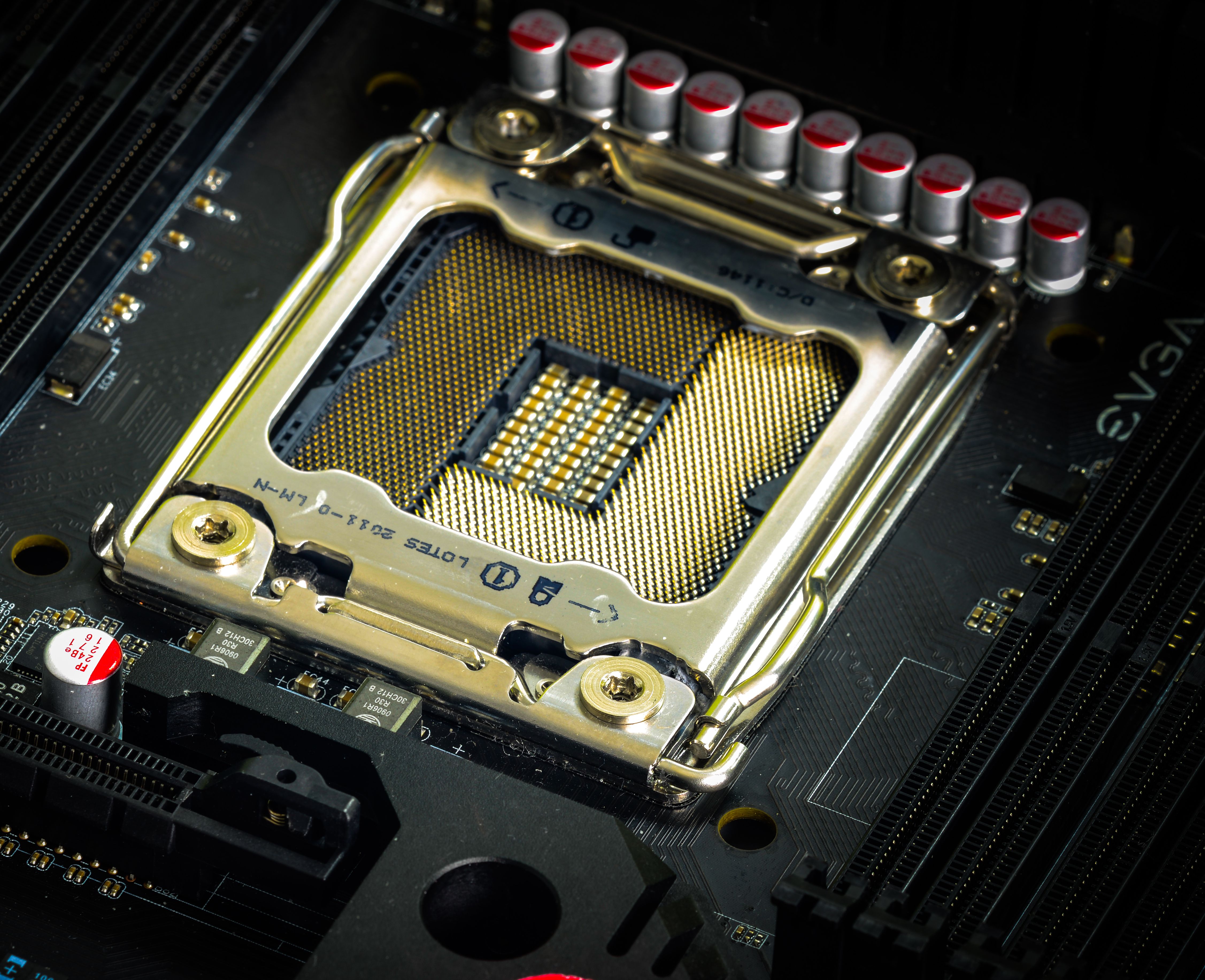
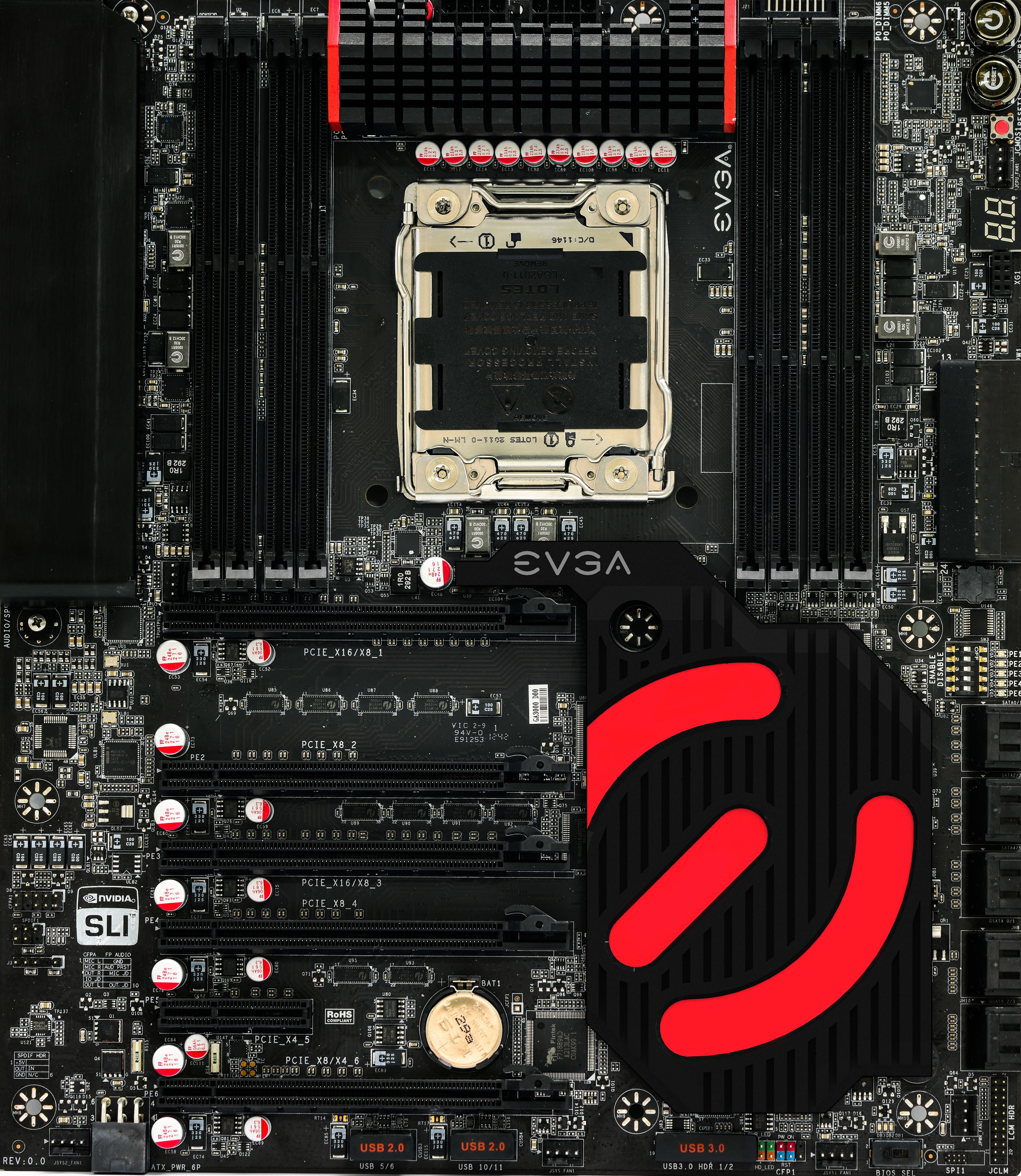
Image 2-4: First EVGA DARK series motherboard, for Intel SandyBridge-E/IvyBridge-E X79 platform.
This guide will showcase the newest addition X299 DARK. X299 DARK is geared to be a maximum performance HEDT platform capable of crushing performance records, and delivering stable operation both for demanding every day content creation/gaming purposes and for unlimited ranges of ambient – extreme overclocking.
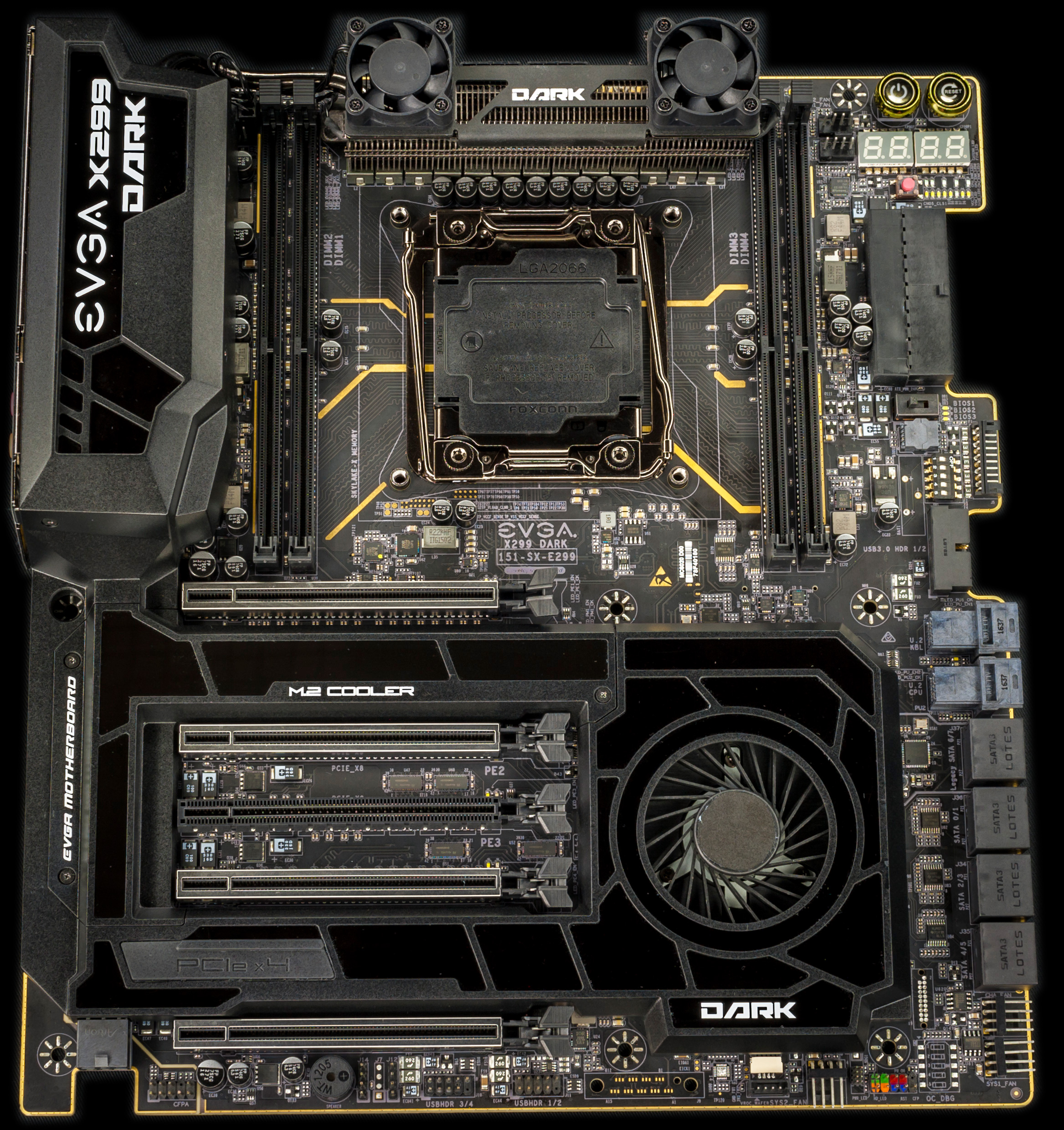
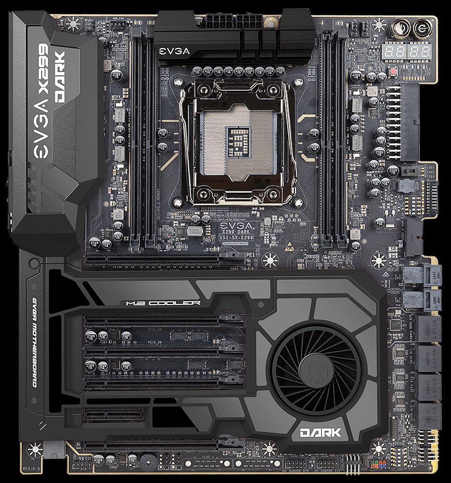
Image 5: EVGA X299 DARK Motherboard in retail configuration
It’s a full ATX size with dimensions measuring 304.8 × 276.7 mm. This is slightly more than typical ATX board, but well within limits of full-size 304.8 × 304.8 mm EATX form-factor dimensions.
While using HEDT motherboards with multicore CPUs in compact system builds is not impossible, this platform is more targeted for larger footprint builds, with rich I/O functionality and support for multiple PCIe devices like graphic cards, NVMe drives or networking controllers. X299 DARK is built to be a maximum performance HEDT platform built for latest generation and most demanding games, content creators, graphic designers and CAD/CAM design engineers.

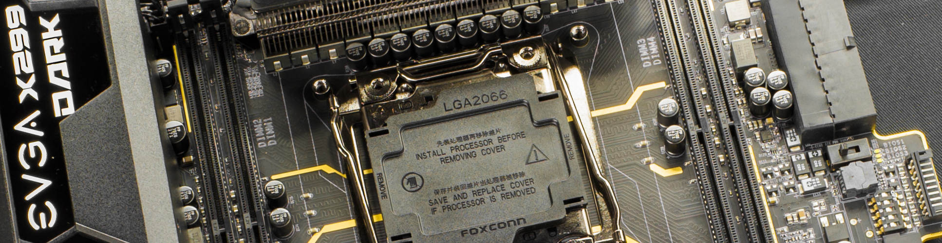
Image 6: Rear I/O with airduct cover and shielding
I/O side Clear CMOS button allow clearing BIOS settings even without chassis disassembly. This button function is duplicated to small red tact button near the diagnostic LED display as well.
Rear panel features eight USB3 ports, with two of them having 10 Gbps bandwidth (red Type-A port and Type-C port) and rest six at 5 Gbps. Each USB port capable delivering 2.5 Amp at nominal 5V. Every port have individual power protection, so even if your device draw too much power, rest of the system and I/O remain functional. There is no support for USB PD charging or high power delivery thru USB 3.0 ports.
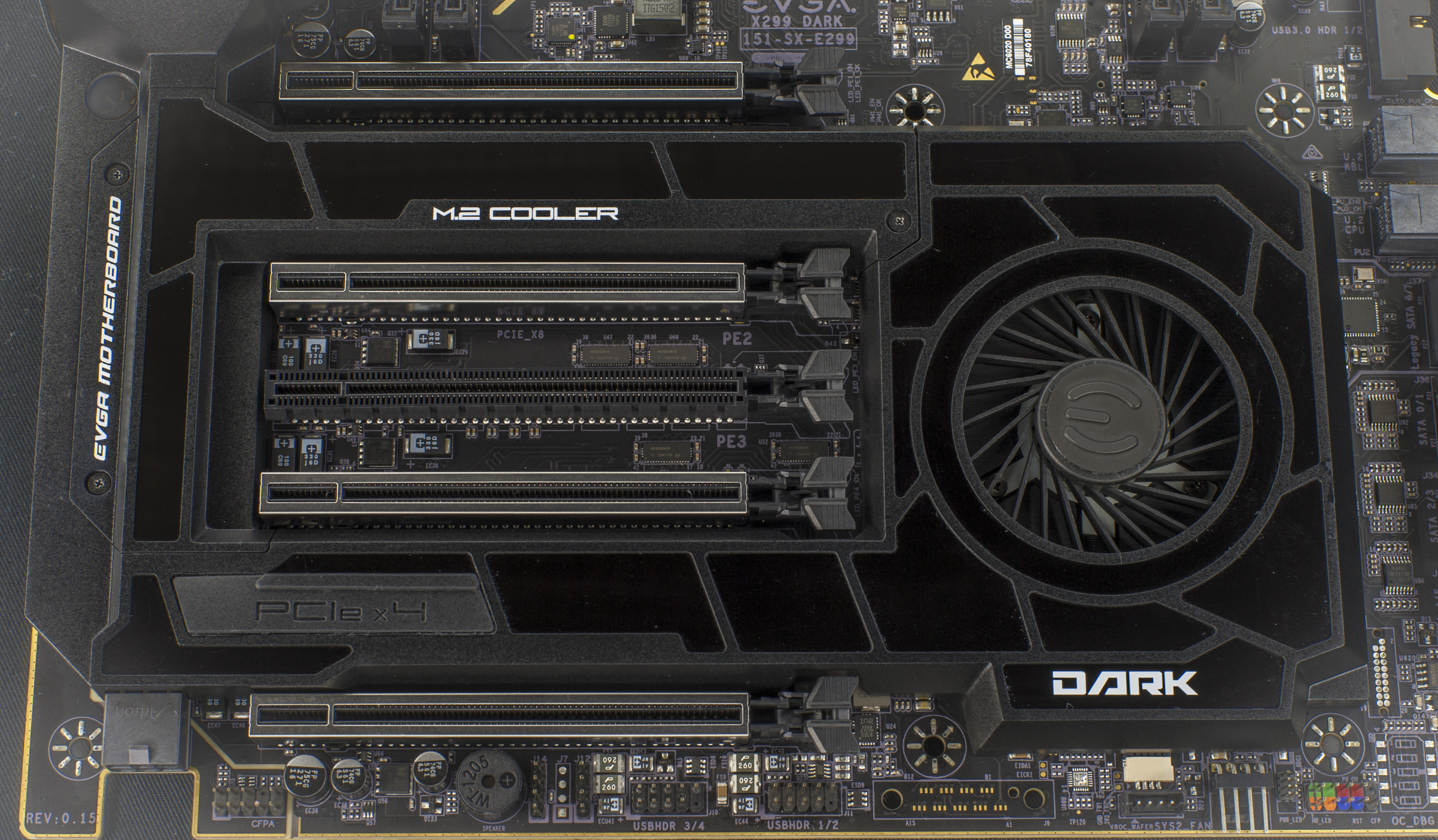
Image 7: PCIe x16 mechanical slots and M.2 cooler airduct system.
Unlike most of other boards on the market, X299 DARK has the ability to exhaust air from the chassis thru vented areas near the audio connector block. The I/O cover has a dual purpose to aid in this, also using internal channels for airflow. Active intake flow for chassis air is provided by large fan above the PCH. PCH itself may take just few watts of power, so it does not demand active cooling. Fan is pushing most of the air thru the cover’s air channels thru the M.2 storage slots PM1 (between PE1 and PE2 ×16 slots) and PM2 (behind PE slots on the right side). Inner design revealed in detail here.
Of course, PCH and VRM fans speed is fully adjustable to allow desired operation. If system chassis provide good airflow already, these fans can be switched off to reduce the noise from the rig.
Bottom row of the chassis connectors feature auxilary ports in next order (left to right):
- CFPA – front chassis audio connector
- Buzzer – diagnostics buzzer for BIOS testing purposes.
- J14 – reserved test header for manufacturing purposes, 4 pin male header
- J12 – reserved serial port for monitoring onboard stats, 4 pin male header
- J10 USBHDR 3/4 – USB 2.0 chassis header for Port 3 and 4
- J11 USBHDR 1/2 – USB 2.0 chassis header for Port 1 and 2
- VROC_WAFER – VROC key shrouded header, 4 pin male header
- PCH_FAN – white PWM PCH fan header, 4 pin male right-angle header
- SYS2_FAN – standard 4-pin right-angle PWM/DC Fan header.
- Chassis header – header for PWR_ON, HDD LED signals and PWR_ON, RESET buttons.
There are five full-size x16 mechanical PCIe slots, and an additional x4 PCIe slot hidden under the rubber cover between PE4 and PE6. All PCIe slots supports a full range of PCIe speeds, from Gen1 (2.5 MT/s per lane) to Gen3 (8 MT/s perlane). With Core i9 CPU installed, all five slots can operate at x8 electrical width.
- PE1 slot share lanes with PE2.
- PE4 slot share lanes with PE3.
- PE6 slot share lanes with PM2 M.2 slot.
- PM1 slot shared witth PU1 U.2 port.
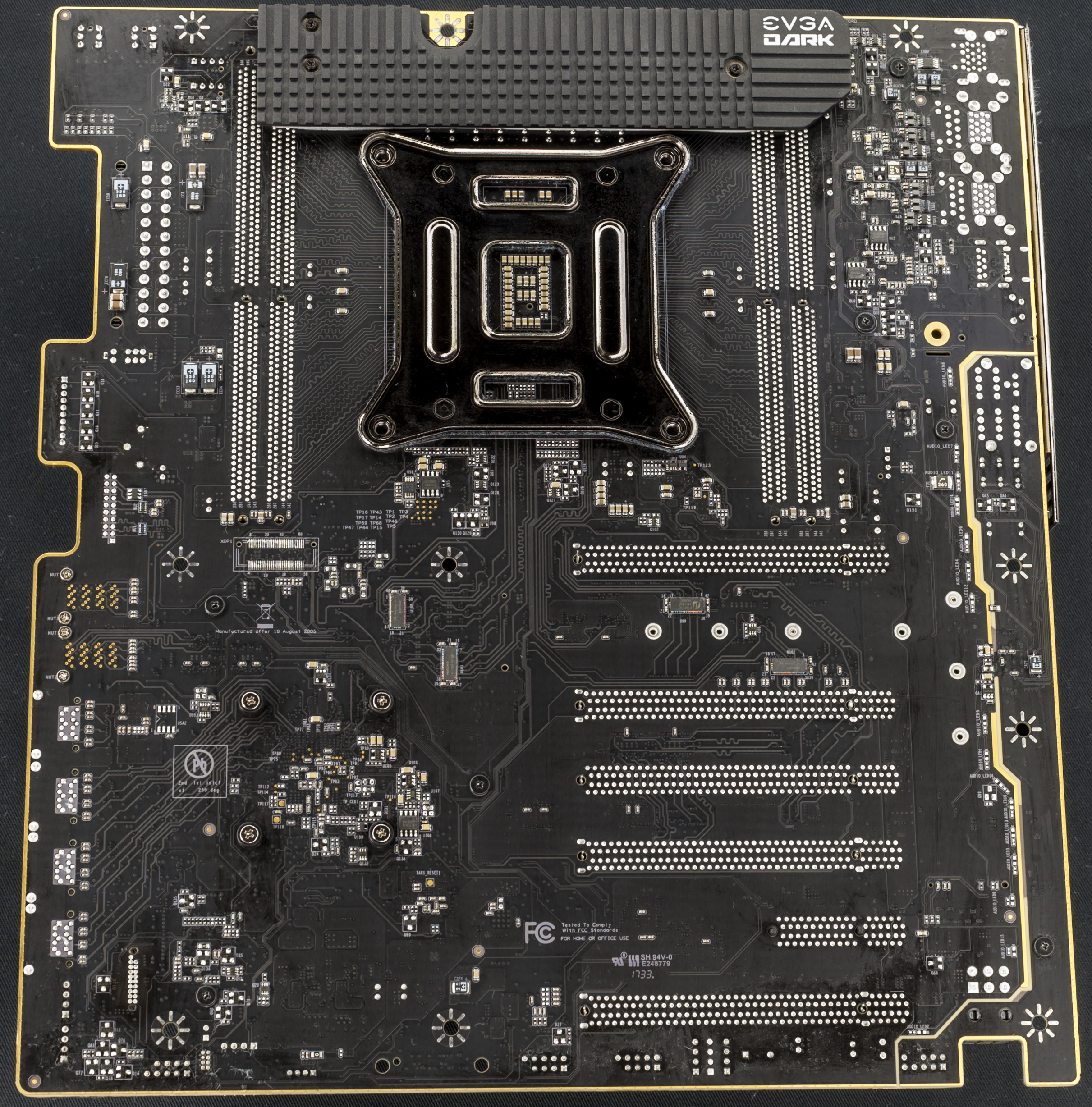
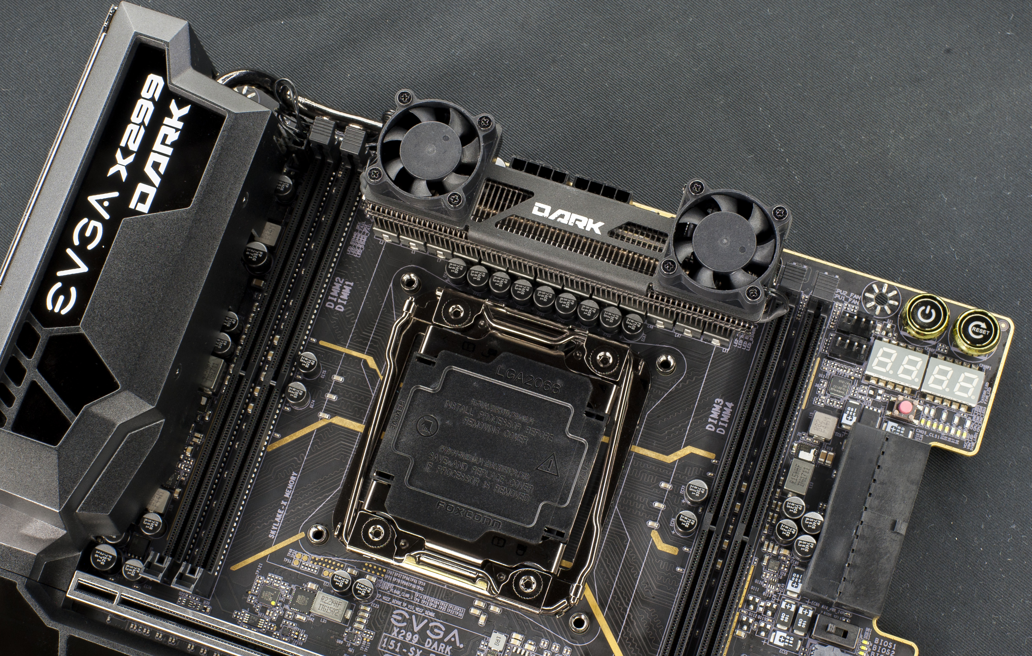
Image 8-9: Bottom side of the motherboard and CPU socket area.
Bottom side of the motherboard is reinforced with a massive aluminum CPU VRM heatspreader plate, mated with PCB passive components over thick thermal pad. Finned surface can help to shave few degrees and spread heat over larger area.

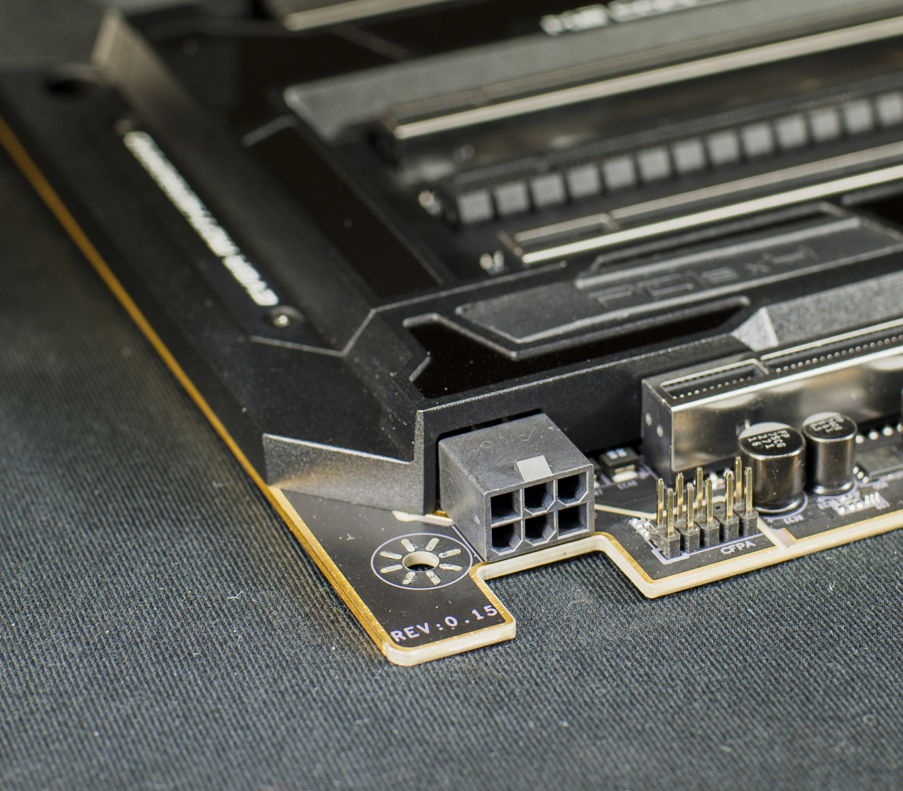
Image 10-11: Right-angle PSU power entry 24-pin and 6-pin connectors for clean cable managment
All connectors on the right side of the motherboard are right-angled, to allow for easy and clean cable management. Some cases might lack additional spacing, so the board has an additional cutouts for 24-pin power entry PSU cable and internal USB3.0 cable to chassis front panel. Right angled 24-pin connectors were first introduced to consumer motherboards by EVGA in 2011 (P67 FTW and SLI boards). Same cutout approach is used for bottom corner 6-pin PCIe power connector. This connector mates with standard 6-pin ATX VGA power cable, to provide an additional power source for PCIe slot +12V power.
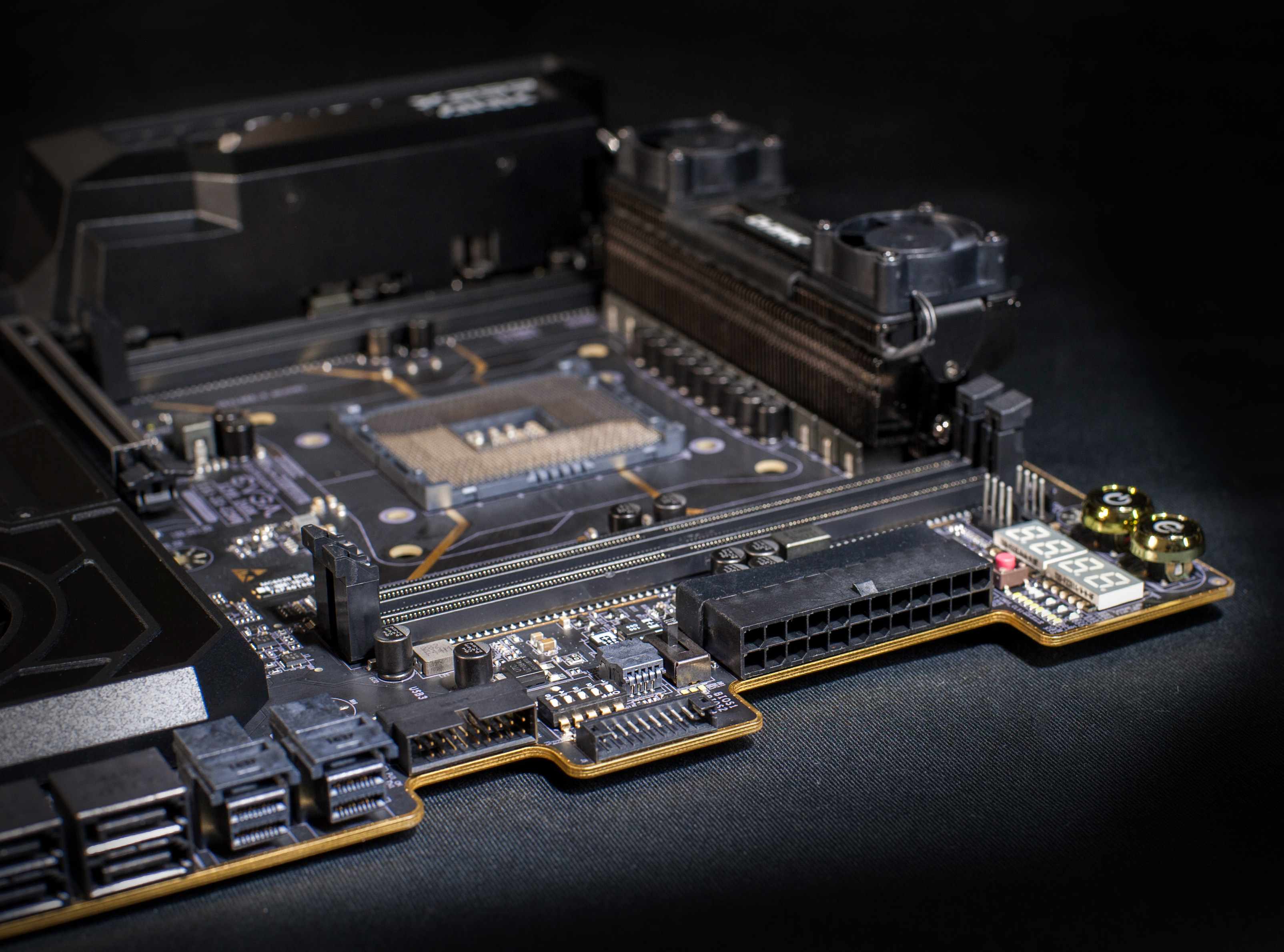
Image 12: Top OC friendly user configuration area.
80Port diagnostics, control buttons and switches, BIOS socket – all these user accessible items are located on the top area, so there is no need to remove devices from PCIe slots to reset the board or troubleshoot BIOS settings. ProbeIt header can help with key important voltages monitoring, while PCIe disable switches can help to troubleshoot which slots contain the failed device that prevent system to finish the POST sequence.
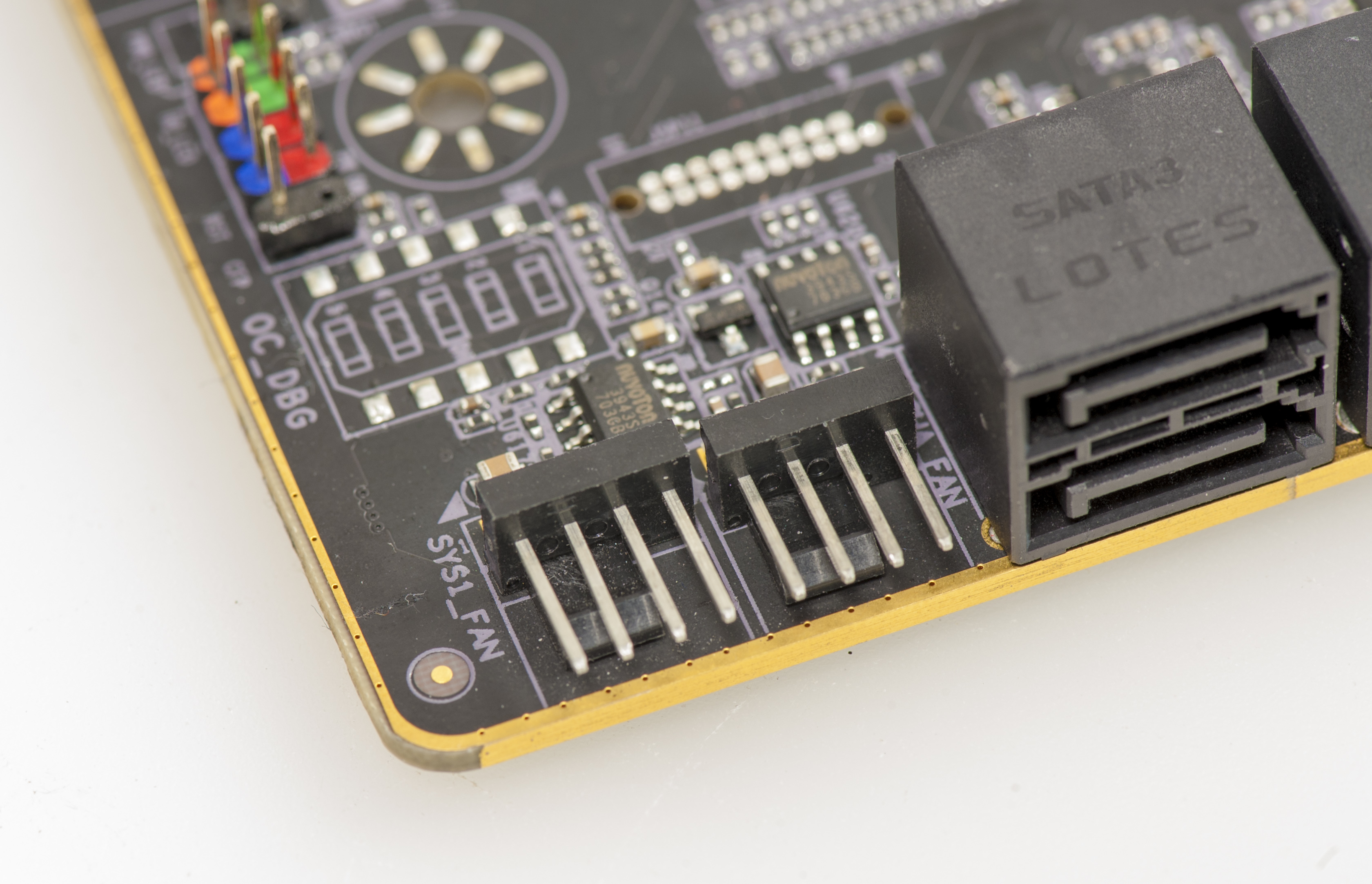
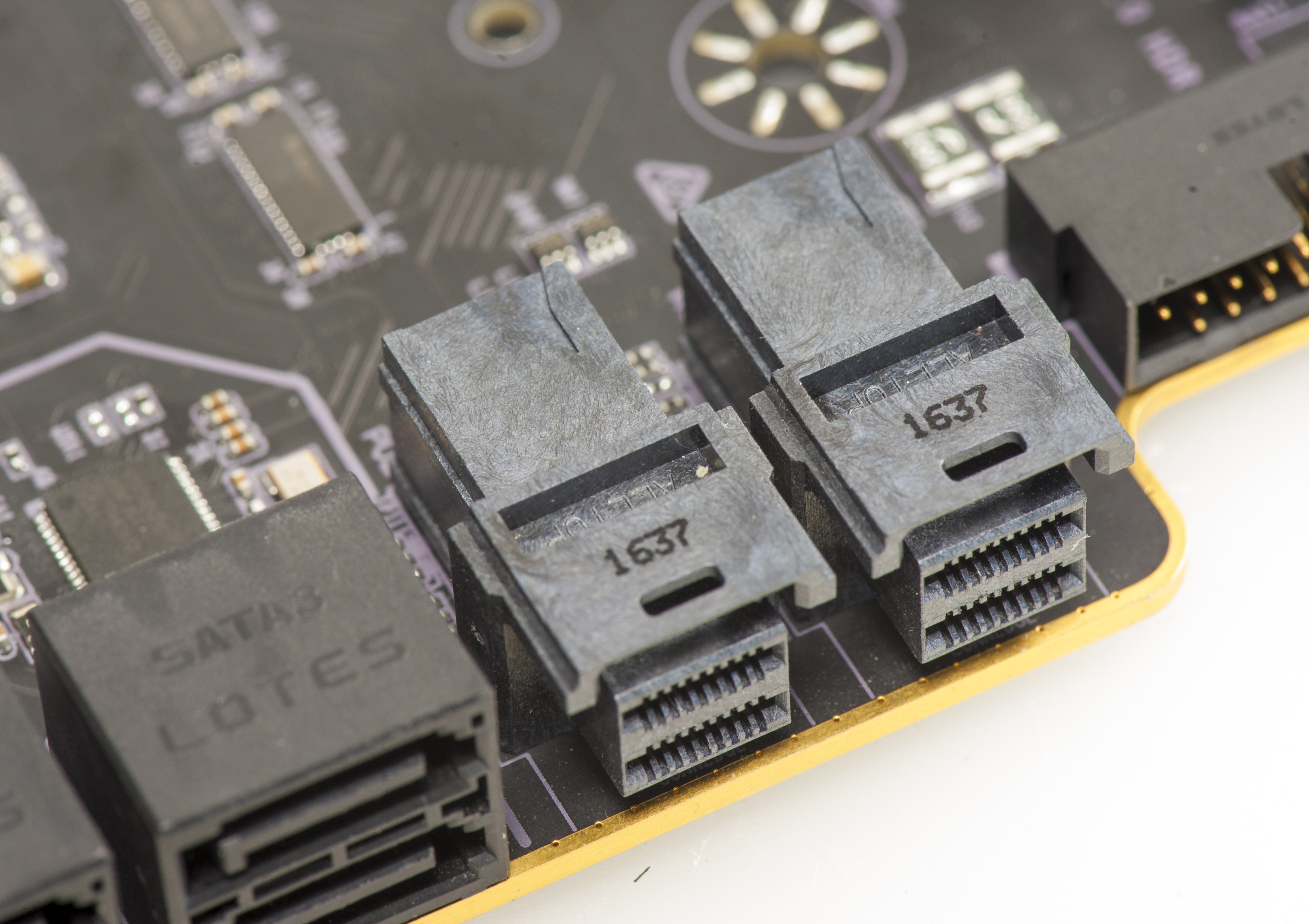
Image 13-14: Right-angle 4-pin fan headers, SATA ports and U.2 NVMe storage ports
X299 Dark board is designed to meet modern 2017-2018 year storage demands, with two 32 GBit/s NVMe U.2 ports with flexible lane configuration. There are also two traditional Socket-M M.2 sockets for mainstream onboard SSD drive options. Dark board does not use expensive PLX PCIe bridge, so actual interface availability depends on installed processor type and lanes available. This is covered in detail here.

Image 15: VRM heatsink assembly with heatpipe on EVGA X299 DARK.
Main CPU power regulator has 12 phases to easily meet high current demands for high-end Core i9 X-series processors, even under the most extreme LN2 cooling conditions. Additional fans were designed in for the worst case scenarios with watercooled CPU and zero external airflow around the board. Massive stacked fin array also coupled with rear I/O heatsink by the copper heatpipe. All this effort is to ensure good thermal margins for the board when under heavy overclocking stress, no matter how much current the CPU may need.
It’s safe to say that the days when decorative heatsink was enough to cool modern multicore hi-end CPU are over. This affects both Intel and AMD, so in the coming years we are more likely to see heavy finned VRM heatsinks on the motherboards, just like today on EVGA X299 DARK.
If the chassis provides decent airflow (for example with array of fans located on top, above the VRM), then the onboard VRM fans can be turned off or set to a very low speed by BIOS settings to preserve quiet operation.

Image 16: Available backplate mount mechanism options for Socket LGA2066.
Talking about cooling, the board also comes with an additional backplane that has no square 80 × 80 mm threaded LGA20xx inserts. This is useful for custom cooling solutions that either do not use same M4 thread or use own their own custom backplate system.
Be careful not to touch socket pins under any circumstances. Bent or damaged socket pins are not covered by manufacturer warranty.
If you need to swap the ILM backplate, you just need 6-point T-20 screwdriver. If you already have CPU installed, unlock both ILM levers to release to ILM loading pressure. If there is no CPU, levers can remain in the locked position. Unfasten four captive nuts with T-20 driver and remove the bottom backplate. Align alternative backplate under the board so it fits to 4 socket holes and fully parallel to board PCB surface. Put top ILM mechanism and fix it on the board by fastening nuts with same T-20 driver.
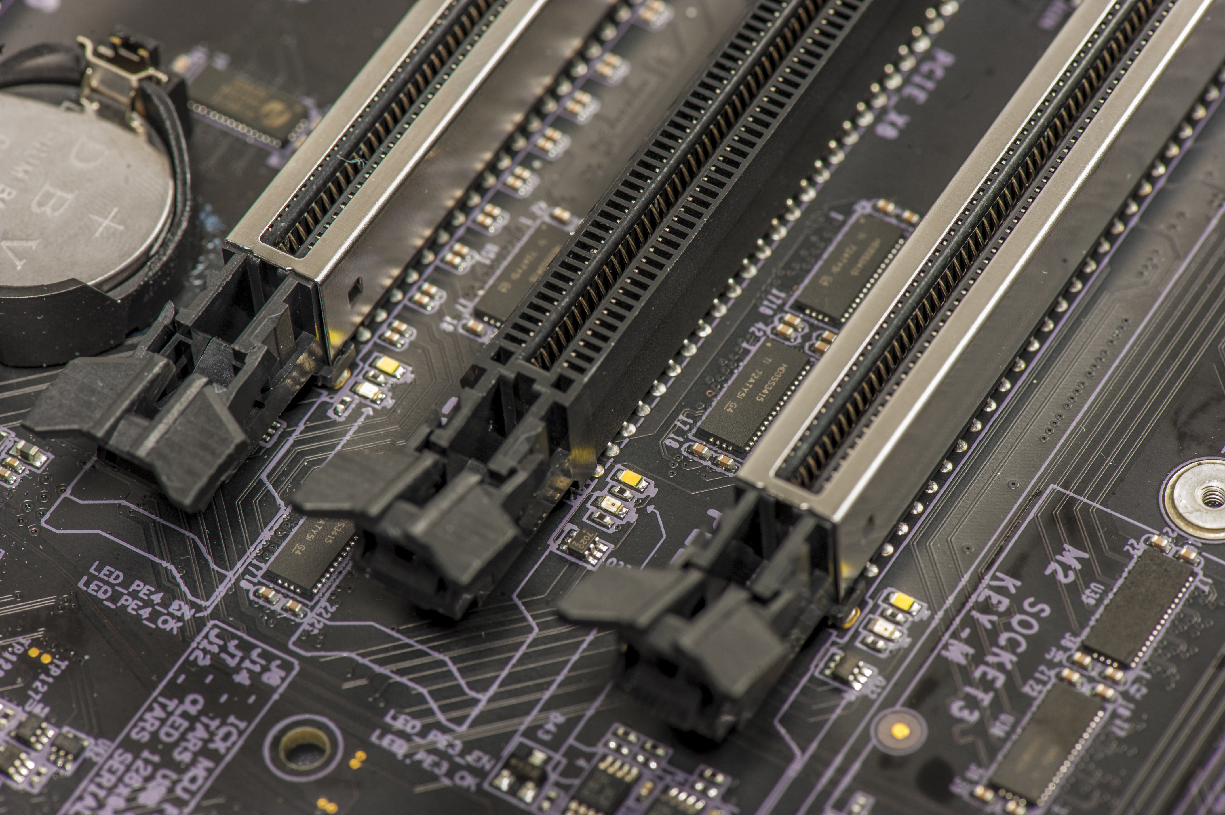
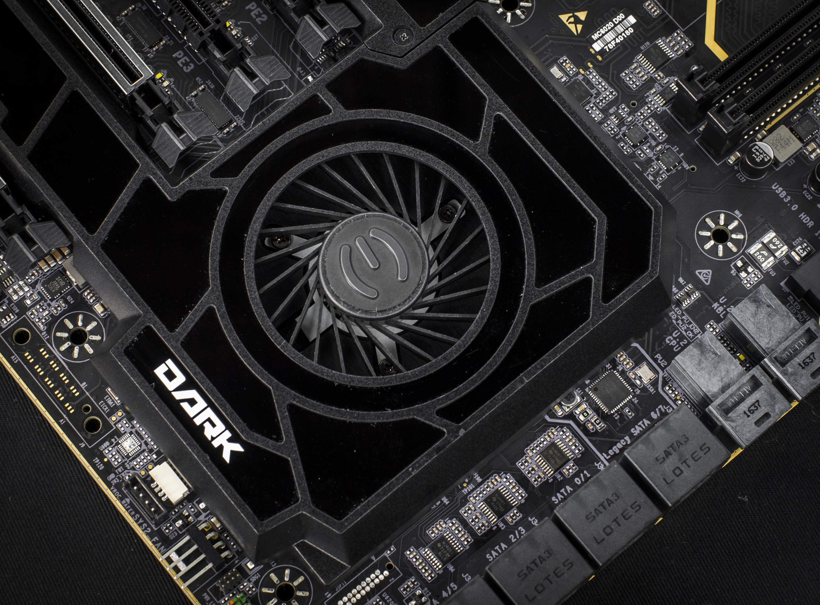
Image 17-18: PCIe slots with shielding, PCIe status LEDs and PCH fansink assembly
Just like any 7th generation Core X-series HEDT motherboard EVGA X299 DARK is based around Kabylake PCH, which in this case bearing X299 Chipset name. All previous HEDT platforms, like Intel X79/SandyBridge-E/IvyBridge-E or Intel X99/Haswell-E/Broadwell-E reused PCH from the EP server/workstation lineup, while this time on X299 board get latest generation desktop PCH with additional USB3/PCIe lanes and features.
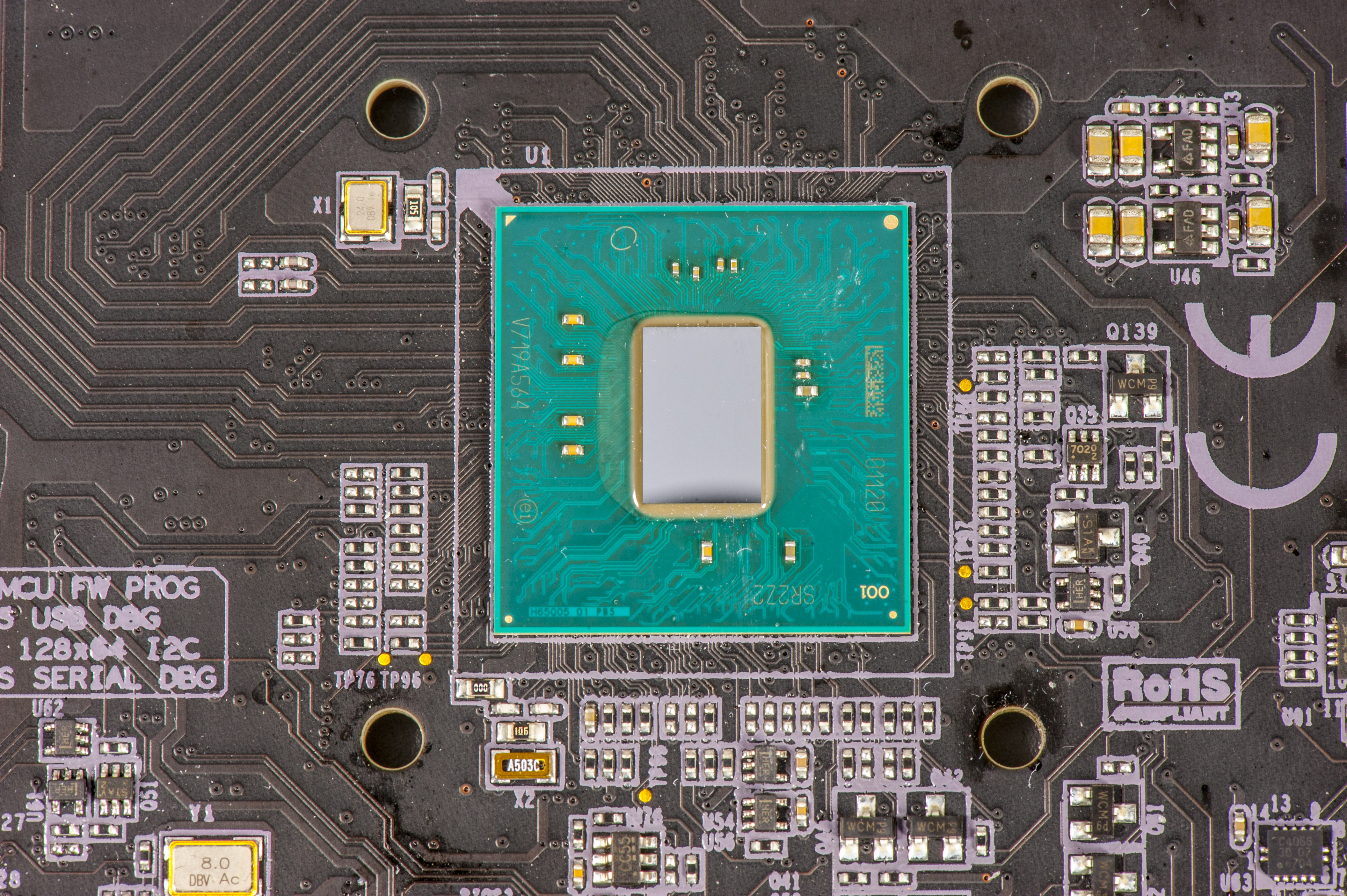
%(imgref)Image 19-20: Core of the motherboard, Intel X299 SR2Z2 PCH manufactured on 22 nm fab node.
Comparison on Intel ARK between X299, Z270, Z370 shows very same feature set, which is no surprise as actual chip even looks the same, just running different firmware/configuration depends on actual board design, be it HEDT, Desktop or performance mobile. Server segment chipset hub that are used in Xeon Scalable platforms, named C620 series based on completely different “Lewisburg” chip.
Processor support
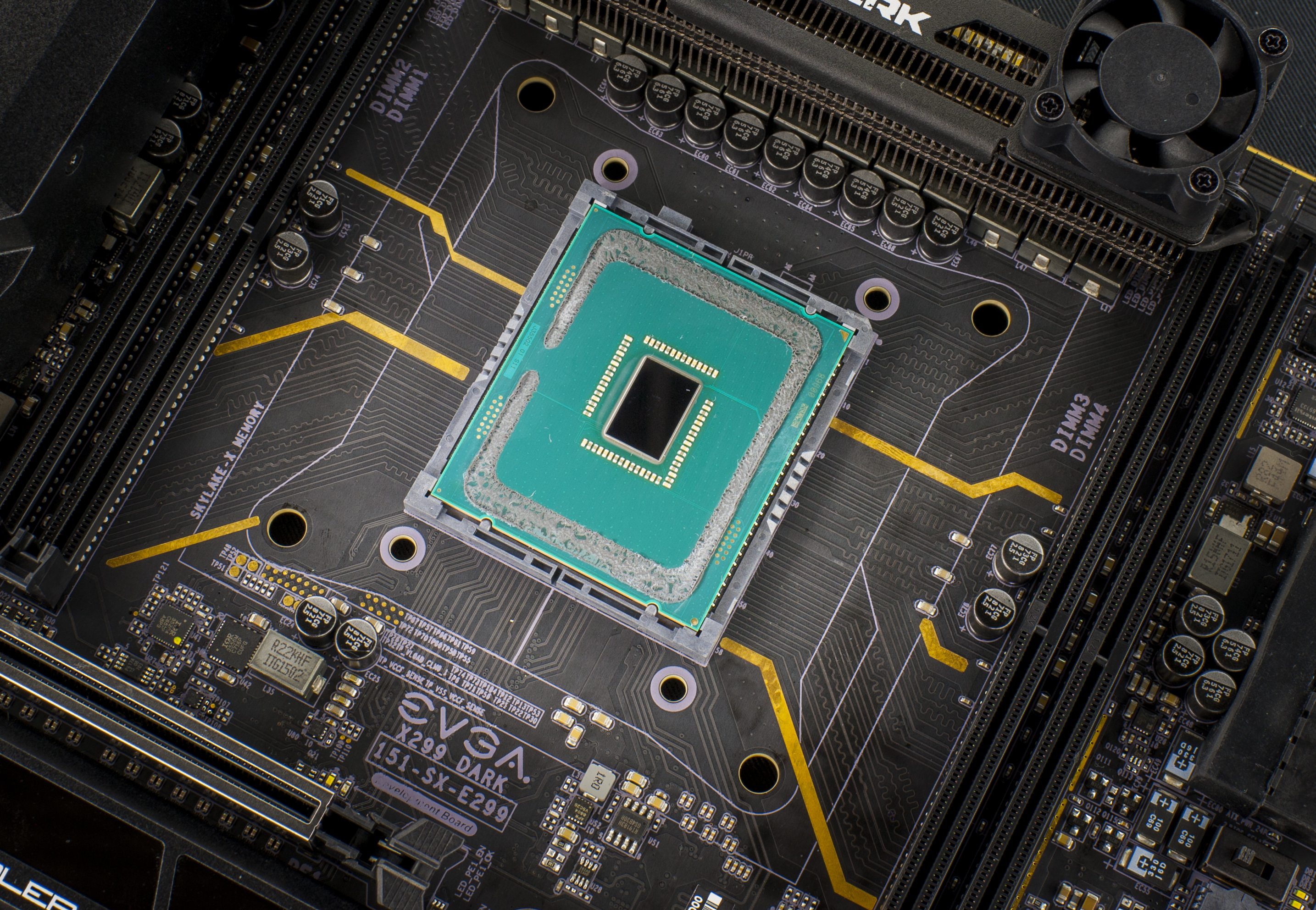
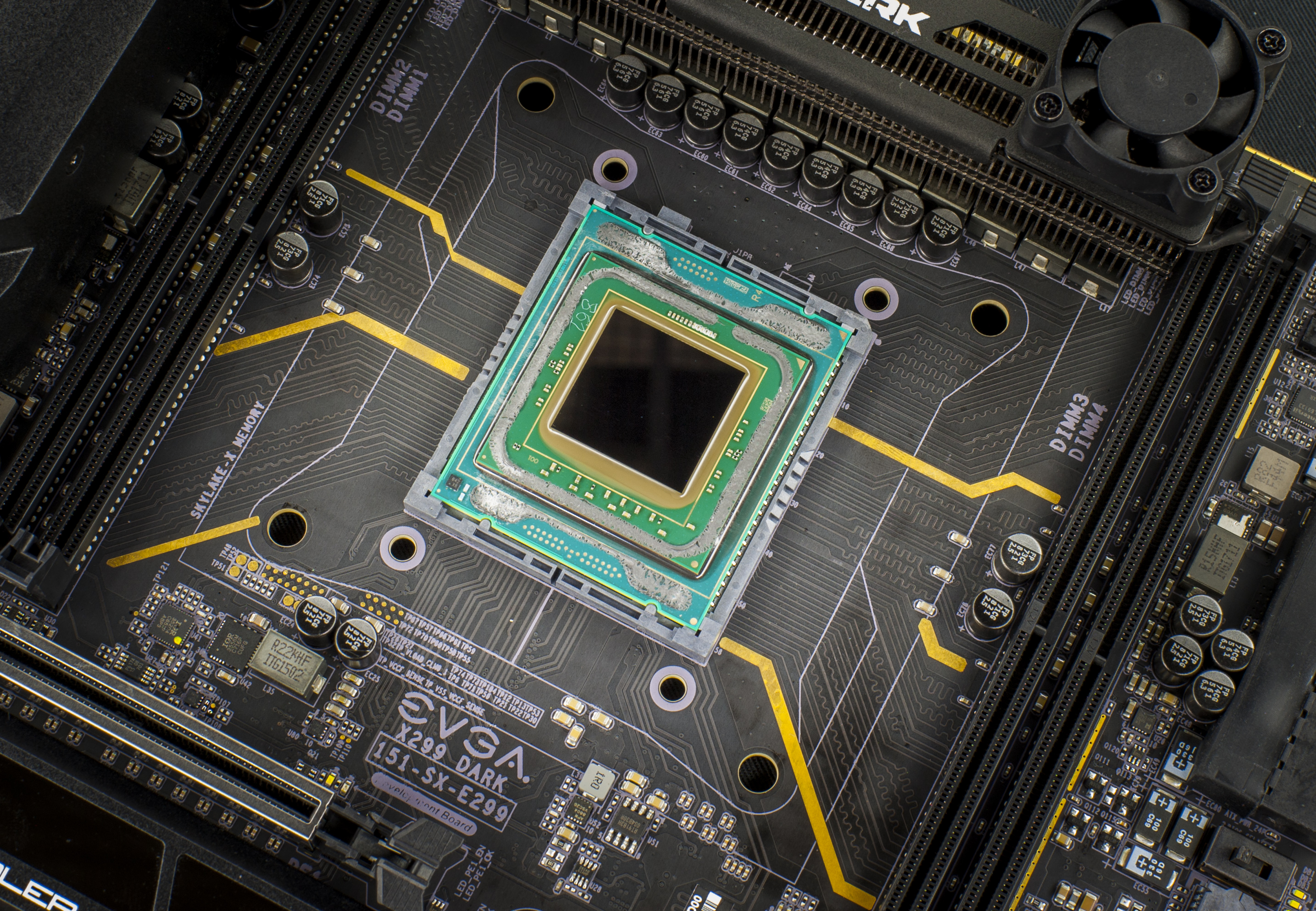
Image 21-22: Two different CPU generations in a same motherboard
Intel’s platform raised many eyebrows with Kaby Lake-X i5 and i7 quad-core processors launch on expensive HEDT segment, but for overclocking it actually makes more sense. Prior to X299, all hardcore overclockers had to invest time and money into two separate platforms. One was mainstream desktop “client” platform, featuring Z-series chipsets and LGA115X socket processors, with until recently were limited to maximum amount of four cores. HEDT platforms like X58, X79, X99, X299 are originally derived from workstation and server high-performance projects. With new X299 now both worlds of consumer and workstation processor generations collide in one product. Now HEDT board allow high-frequency low-core count overclocking with Kaby Lake-X processors and heavy 3D-benchmarking with SLI/Crossfire graphics using Skylake-X i9’s, just swap the processor. If will be interesting to see how this platform evolve next year, as todays mainstream is expanding with new 6-core 8th Generation Coffee Lake processors.
And X299 DARK tested and tuned to work with both CPU types, taking the best from either world. More on available functionality and onboard connectivity will be covered in next sections. Currently available CPU lineup and key features that are enabled on CPU tier listed in Table X.
New E5-1600 V4 series replacement processors, Intel® Xeon W-21xx are no longer supported on the HEDT Intel X299 platform. These workstation CPUs now require enterprise grade chipset motherboard, such as Intel C422. These workstation boards also in agreement do not support HEDT Core-X CPUs.
Also main server multisocket-capable processors such as Xeon E5-26xx V4 series are also replaced by brand new Skylake-SP family using completely new LGA3647 Socket P and C620 chipsets.
| Feature | i5-7640X | i7-7740X | i7-7800X | i7-7820X | i9-7900X | i9-7920X | i9-7940X | i9-7960X | i9-7980XE |
|---|---|---|---|---|---|---|---|---|---|
| Architecture | Kaby Lake-X | Skylake-X LCC | Skylake-X HCC | ||||||
| CPU Cores(HT) | 4\4 | 4\8 | 6\12 | 8\16 | 10\20 | 12\24 | 14\28 | 16\32 | 18\36 |
| CPU LL(Last level) Cache | 6 MB | 8 MB | 8.25 MB | 11 MB | 13.75 MB | 16.5 MB | 19.25 MB | 22 MB | 24.75 MB |
| PCIe lanes | 16 x Gen 3 | 28 x Gen 3 | 44 x Gen 3 | ||||||
| Overclocking | Fully unlocked, LN2 ready | Fully unlocked, LN2 ready | |||||||
| BCLK OC | 60-300+ | 93-107 or 117-133 or 154-177 MHz | |||||||
| Memory OC | 4133+ MHz | 4000+ MHz | |||||||
| SLI-ready | 2-way | 3-way | 4-way | ||||||
| CPU MSRP | $243 | $350 | $389 | $599 | $999 | $1199 | $1399 | $1699 | $1999 |
Table 2a: Processor functionality summary.
All X299 DARK motherboards support updated Skylake-X line-up of Core i9 CPUs, launched in Q4’2018.
These CPUs, even most affordable i7-9800× 8-core SKU now have 44 PCIe lanes, so there is no reduction of I/O functionality with new CPUs.
| Feature | i7-9800X | i9-9820X | i9-9900X | i9-9920X | i9-9940X | i9-9960X | i9-9980XE |
|---|---|---|---|---|---|---|---|
| Architecture | Skylake-X HCC | ||||||
| CPU Cores(HT) | 8\16 | 10\20 | 10\20 | 12\24 | 14\28 | 16\32 | 18\36 |
| CPU LL(Last level) Cache | 16.5 MB | 19.25 MB | 22 MB | 24.75 MB | |||
| PCIe lanes | 44 x Gen 3 | ||||||
| Overclocking | Fully unlocked, LN2 ready | ||||||
| BCLK OC | 93-107 or 117-133 or 154-177 MHz | ||||||
| Memory OC | 4000+ MHz | ||||||
| SLI-ready | 4-way | ||||||
| CPU MSRP | $589 | $889 | $989 | $1189 | $1387 | $1684 | $1979 |
Table 2b: Q4’2018 Refresh processor support summary.
And last, but not least, 3rd drop-in refresh processors, such as CascadeLake-X Core i9 10th series released in November 2019 work just fine in EVGA X299 DARK motherboards as well after BIOS update.
| Feature | i9-10900X | i9-10920X | i9-10940X | i9-10980XE |
|---|---|---|---|---|
| Architecture | CascadeLake-X HCC | |||
| CPU Cores(HT) | 10\20 | 12\24 | 14\28 | 18\36 |
| CPU LL(Last level) Cache | 19.25 MB | 24.75 MB | ||
| PCIe lanes | 48 x Gen 3 but only 44 are used on X299 DARK | |||
| Overclocking | Fully unlocked, LN2 ready | |||
| BCLK OC | 93-107 or 117-133 or 154-177 MHz | |||
| Memory OC | 4200+ MHz | |||
| SLI-ready | 4-way | |||
| CPU MSRP | $590 | $689 | $984 | $979 |
X299 platform is one of the longest living platforms in Intel’s recent desktop offerings. With November’s addition to a family EVGA X299 DARK supports no less than four different kinds of CPU – Kabylake-X, Skylake-X 7th series, Skylake-X 9th series and CascadeLake-X 10th series.
Available control items in BIOS GUI are also automatically configured, depending on installed CPU:
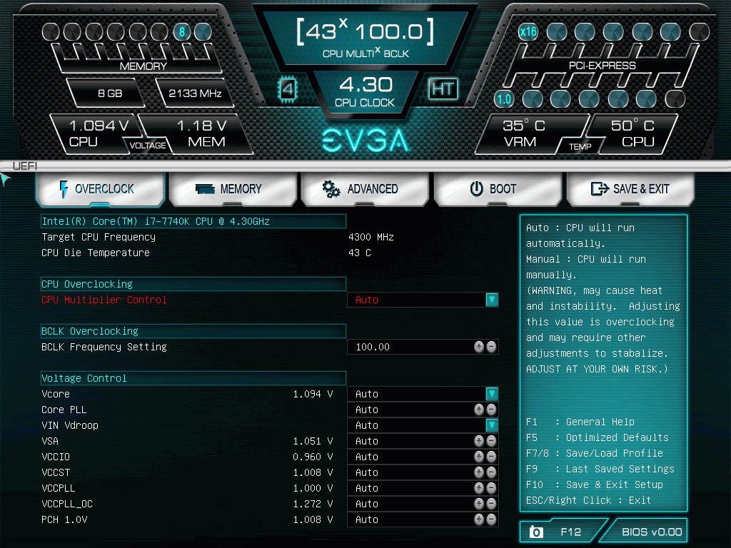
Image 23: Default settings for Kabylake-X processors.
With Skylake-X processor BIOS setup looks similar, with changes in specific control items. BIOS automatically detects installed CPU type and configures available settings menu.
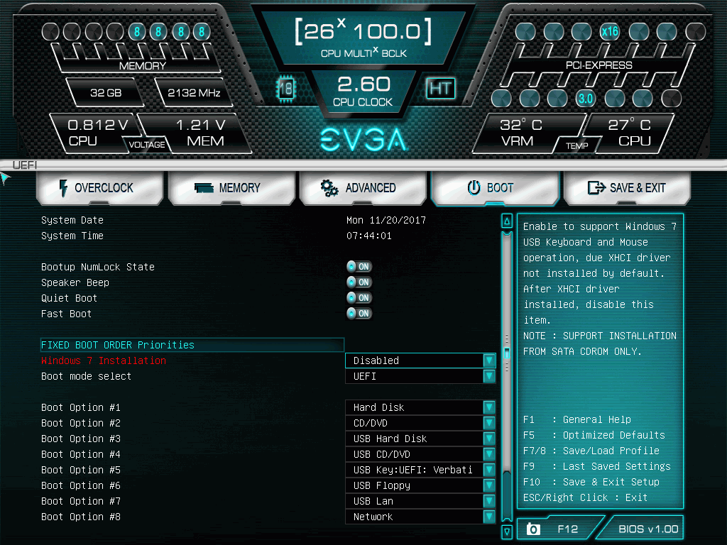
Image 24: Default settings for Skylake-X (right) processors.
Some settings are also automatically adjusted depends on the current operation profile. One of such examples – CPU power limits controls. These are usually available in BIOS and tweaking utility in OS, such as Intel XTU.
Unlike some other boards, on X299 DARK you will not find PL1/PL2 (power limit) settings and other power management settings for CPU in BIOS UI. These limits are maintained by BIOS itself. If you running stock settings then everything follows Intel specifications, but when you do overclocking (that is setting CPU/BCLK ratios and voltages higher than stock defaults) board will take care of power limits, to make sure CPU does not throttle, unless you hit temperature limits.
When replacing CPU with another type (like KabyLake-X to Skylake-X/CascadeLake-X) system will do few additional power cycles and automatically clear all CMOS settings to gracefully reconfigure onboard devices and chipset.
High-speed memory layout
Good memory performance requires good high-speed PCB layout and routing specifications. Additional PCB layers, signal shielding and power quality are all factors that influence the system memory performance. Also leaving hardware alone no overclocking can happen without good BIOS tuning and tweaking the correct settings.
As interfaces and signals go faster, digital design for error-free operation become a challenge. With memory clocks reaching more than 4000 MHz various physics factors and effects come into play and impact the semiconductors operation. Memory speed performance remain the bottleneck due to complex signal integrity issues further amplified with lower DDR4 voltages and higher DRAM density. As we get more processor cores and faster I/O devices, demand for wide memory bandwidth is also getting only stronger. That is one of the reasons why on graphic cards and enterprise market we already see alternative approaches like using HBM memory (AMD Fury and Vega GPUs, NVIDIA Pascal GP100/Volta GV100), MCDRAM (Intel Xeon Phi x200), HMC.
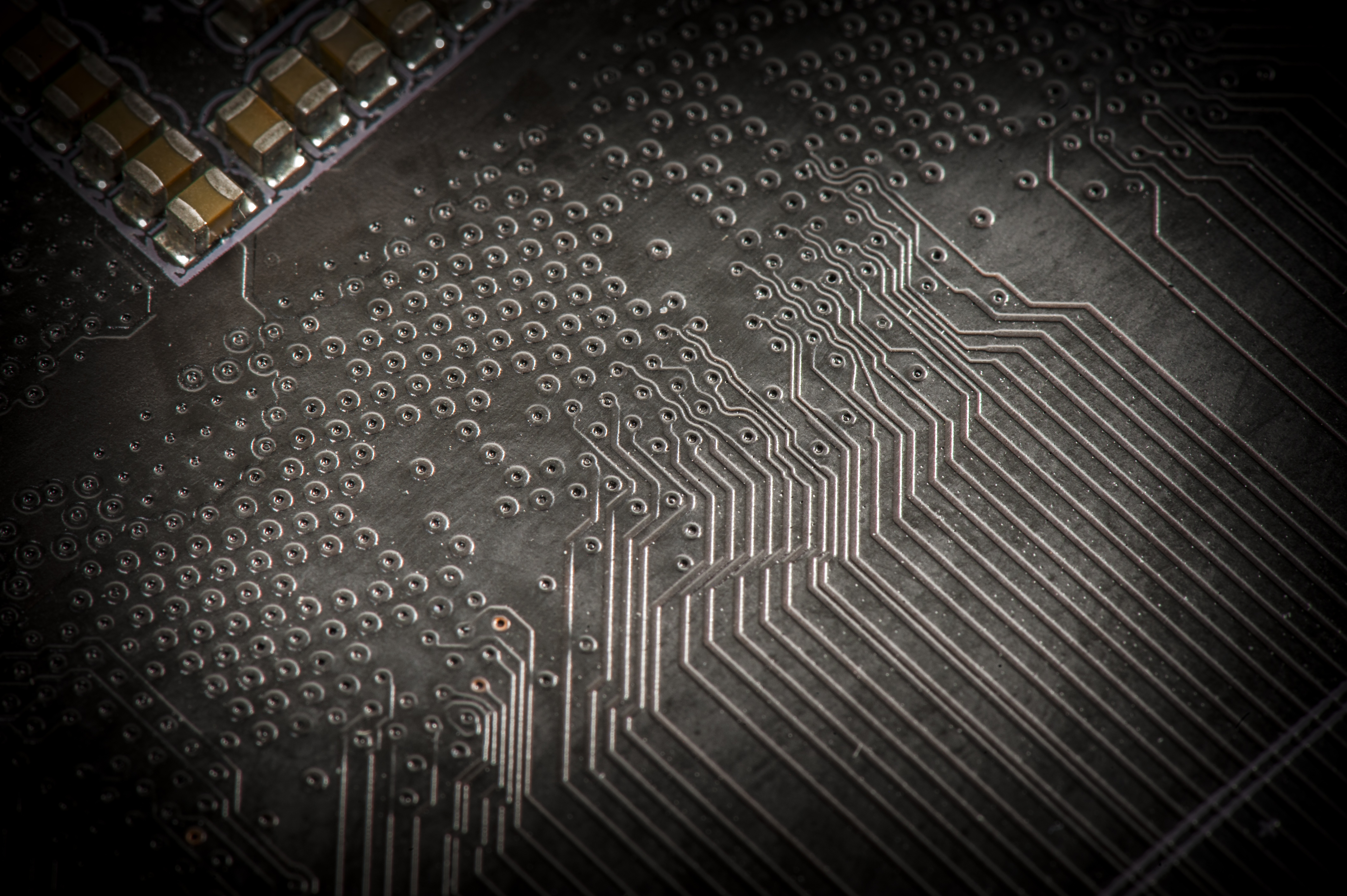
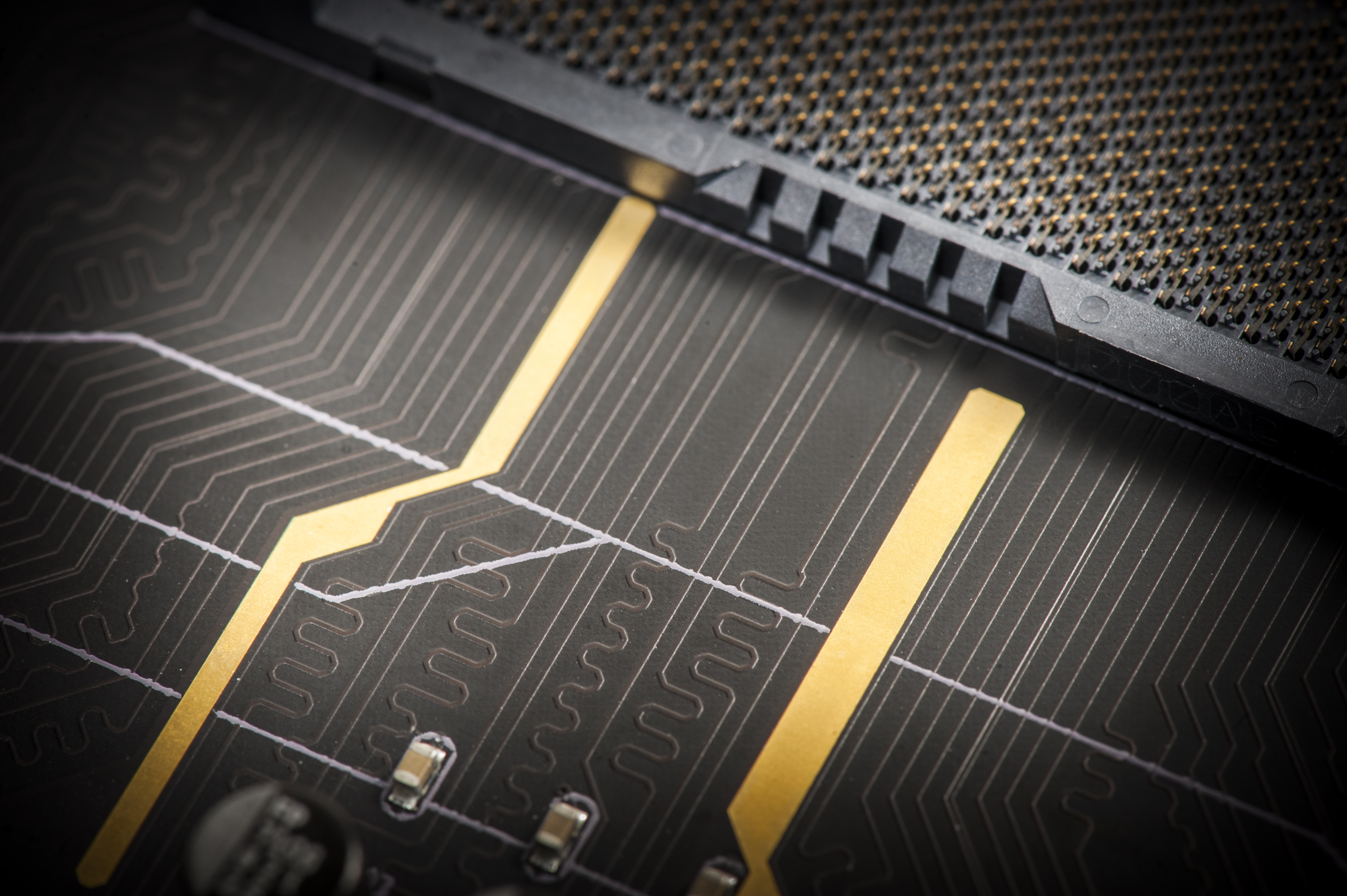
Image 25-26: PCB memory layout routing on the board.
Additional loading to the signals, in form of extra connectors also negatively impact maximum DDR4 frequency. Hence on X299 DARK amount of memory slots is reduced to only one per channel, with total 4 DIMMs. X299 FTW board offer 8 DIMM for the users than need memory capacity larger than 64 GB.
Single DIMM per channel allows faster clocks, beyound 4000 MHz with both CPUs (Skylake-X and Kabylake-X). Typical DDR4 UDIMM today have 8 GByte density, which is not a small amount for typical loads. High loading and workstation scenarios with quad-channel capable Skylake-X can expand with 4 × 32 GByte modules, allowing total memory size of 128 GB.
Great amount of time and effort was dedicated on making automatic XMP operation well for all range of the speeds, including very high frequency ranges like 3733-4000 MHz. All major memory manufacturer has these high-speed modules available, even though real practical benefit is barely (in)visible in any real-life application. Optimum memory speed for any X299 system is around 3200-3466 MHz.
Only unbuffered DDR4 non-ECC UDIMMs with capacity up to 32 GBytes/module are supported. Board will not work with server DDR4 RDIMM or LRDIMM modules, no matter what capacity they are.
VRM design overview, available tuning and hardware controls
Power regulator for CPU and memory on EVGA X299 DARK is based around the brand new Intersil digitally-controlled converter and compact 60ADC Smart Power Stage IC – Intersil ISL99227B. VRM on this board is upsized to 12 phases to handle LN2 extreme overclocking with monstrous 18-core Skylake-X CPU.
Efficient VCORE solution that has a large power margin can also spread thermal stress evenly over larger surface area, making VRM cooling easy task. Power delivery starts from not one but two 8-pin MiniFit.Jr CPU power connectors. These 8-pin MiniFit.JR type connectors rated at 40A of continous current, each.
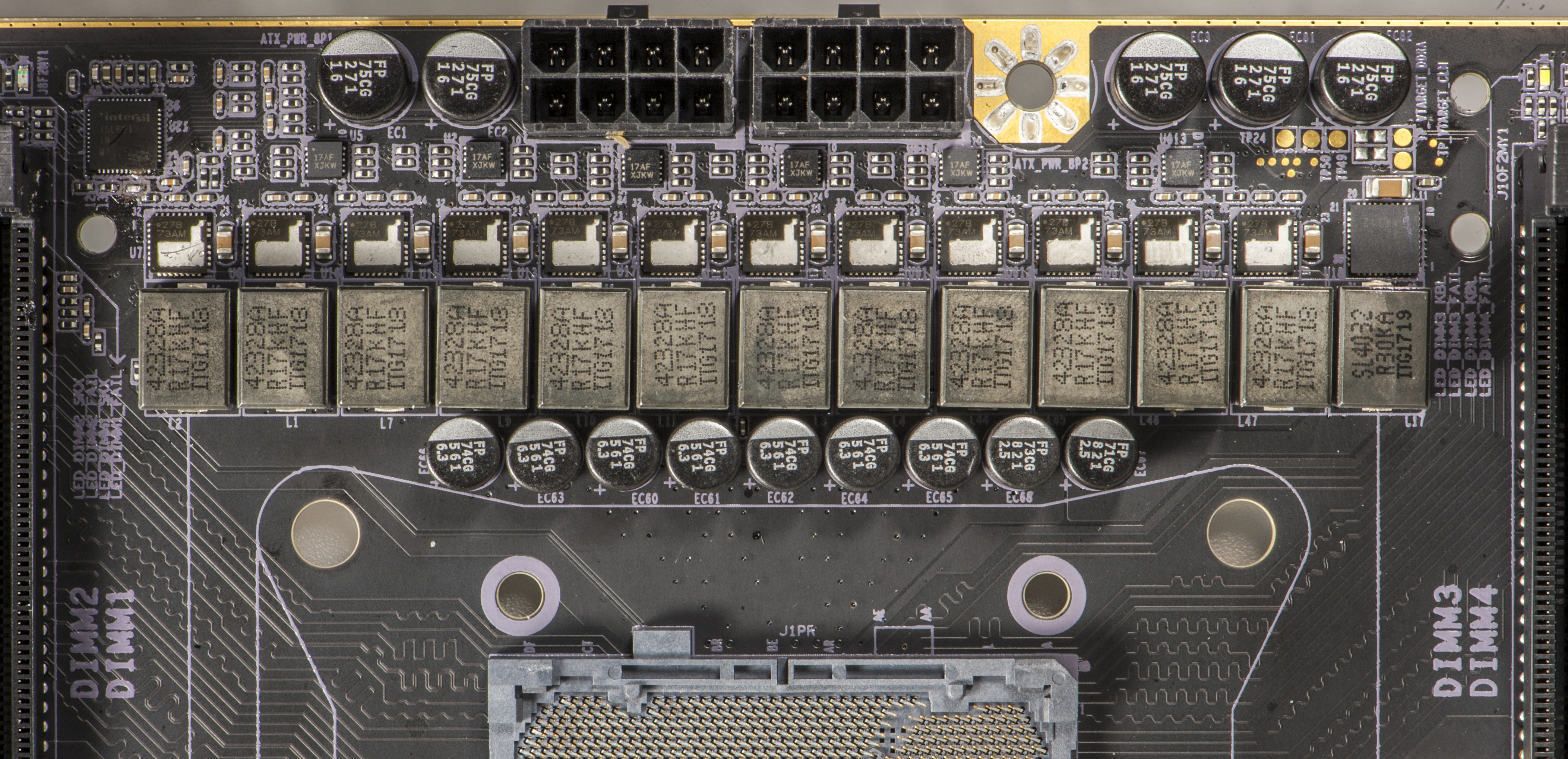
Image 27: Main processor VCORE/VCCIN voltage regulator and power inputs.
Anyone can confirm this by checking manufacturer specification limits of power connector itself, such as Molex 26-01-3116. These are rated from 13A per contact (16AWG standard high-performance PSU wire for CPU power).
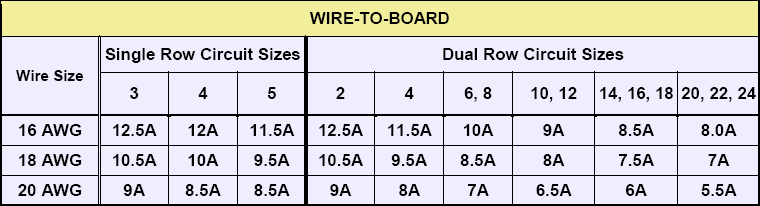
Image 28: Molex 26-01-3116 MiniFit-Jr. current rating specs.
Per table, this means that high-end PSU with 16AWG wires for CPU power cable able to provide 10A * 4 (four of pins used for +12V, four remaining for GND return) = 40 A. This is given a connector temperature rise of 30 °C with all power pins used. With active airflow and decent cable quality, safe current limits are bit higher. Power rating as result is hefty 40 A × 12.0 V = 480 W per connector, or 960 W total power available for CPU. This power can be provided all day long, without worry about going over the specification, with no additional stress on cabling and risk of connector damage.
Power limitations is one the last thing we want during extreme overclocking sessions with a $2000 USD Intel® Core™ i9-7980XE processor.
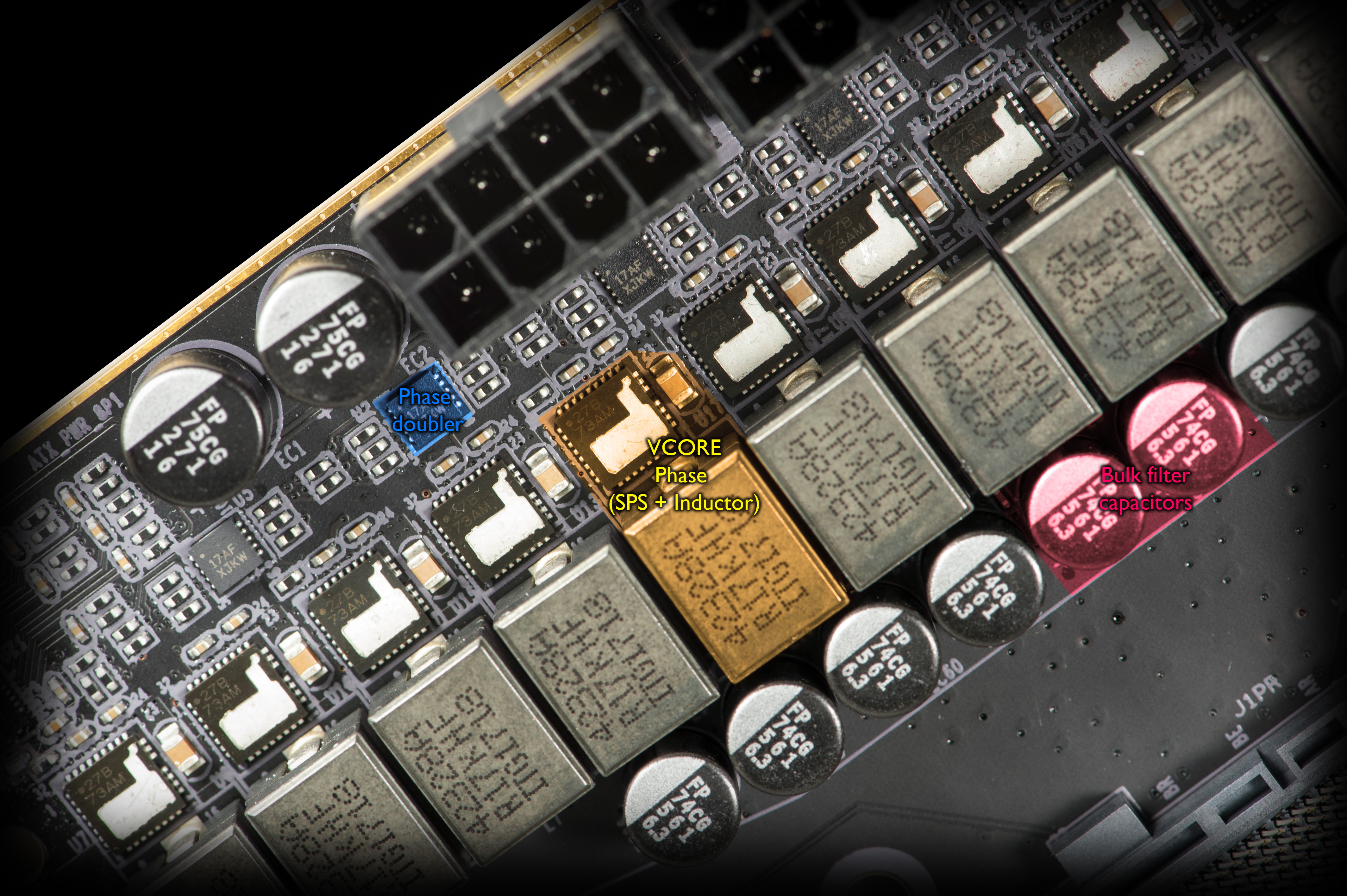
Image 29: Close-up on VCORE regulator circuitry.
Looking closer on the VCORE power stage, we see a set of Smart Power Stages, small set of doublers to multiplex PWM control signal from controller to the Smart Power Stages inputs.Each of these ISL99227B can deliver ~54 Amps of current with operation temperature +80 °C, or ~58 Amps with operation temperature under +50°C.
Power inductor is a top notch ITG AH42328A-R15KHF rated at 71 Amp each, well in line for 60 A specification, per phase. Main low-ESR capacitors used for input and output bulk energy storage are 1st tier Nichicon FPCAP solid-polymer electrolyte type.
But power delivery requirements for modern CPUs do not end just with VCORE. Many additional lower power rails are still important for reliable CPU operation. There are no shortcuts taken on those either.
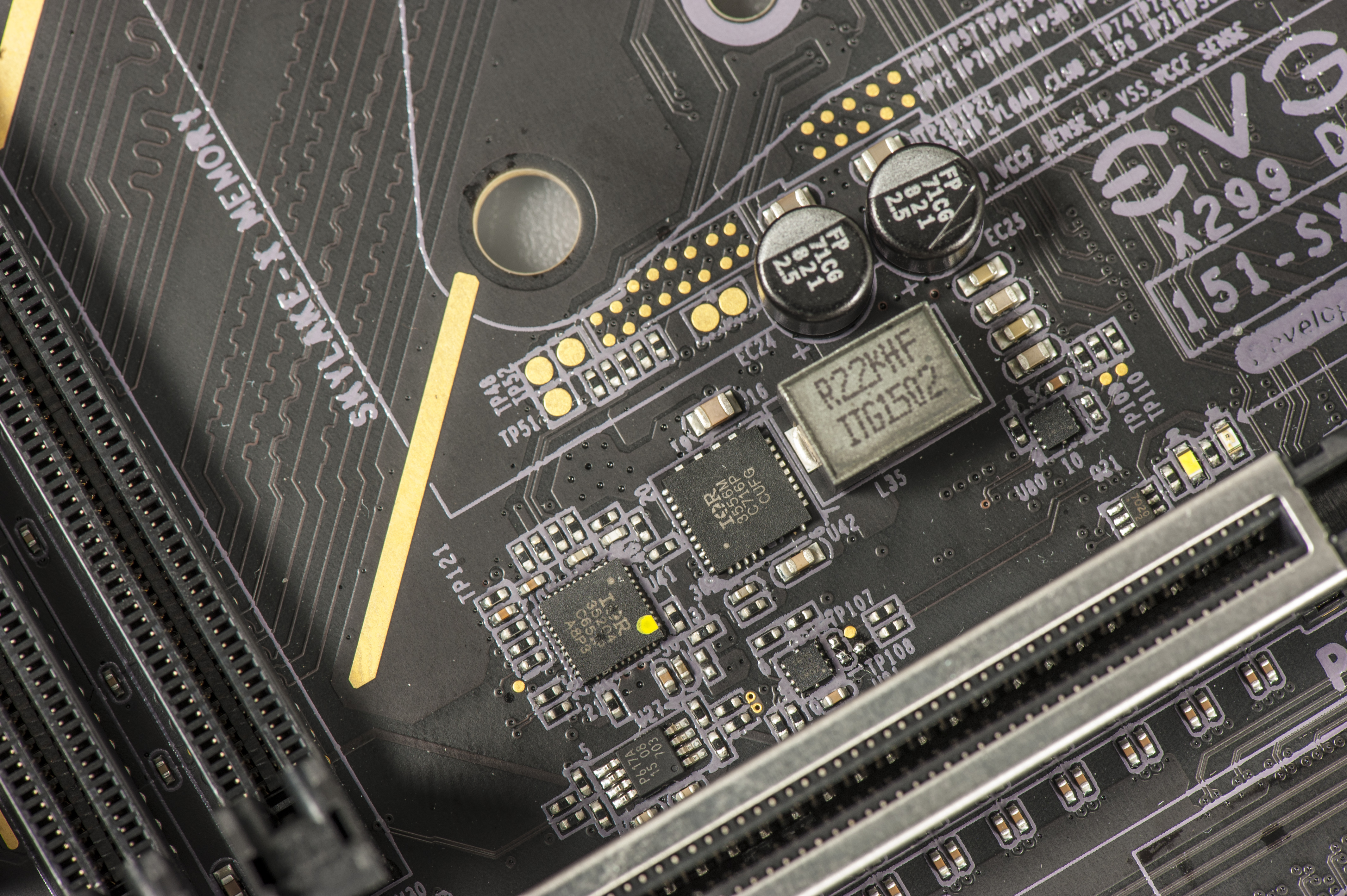
Image 30: EVGA X299 DARK processor’s VCCIO converter.
VCCIO is generated by single-phase proven Infineon/IR35204 controller and 60A IR3555M PowIRstage.
Dual tandem of Intersil ISL69133IRZ and ISL99227 supply adjustable and clean DDR4 DIMM voltage, one at each side. Array of FPCAPs and ceramic capacitors help to clean up the switching supply ripple. Each of these VRMs have lot of thermal and power margin to operate without any heatsink requirements.
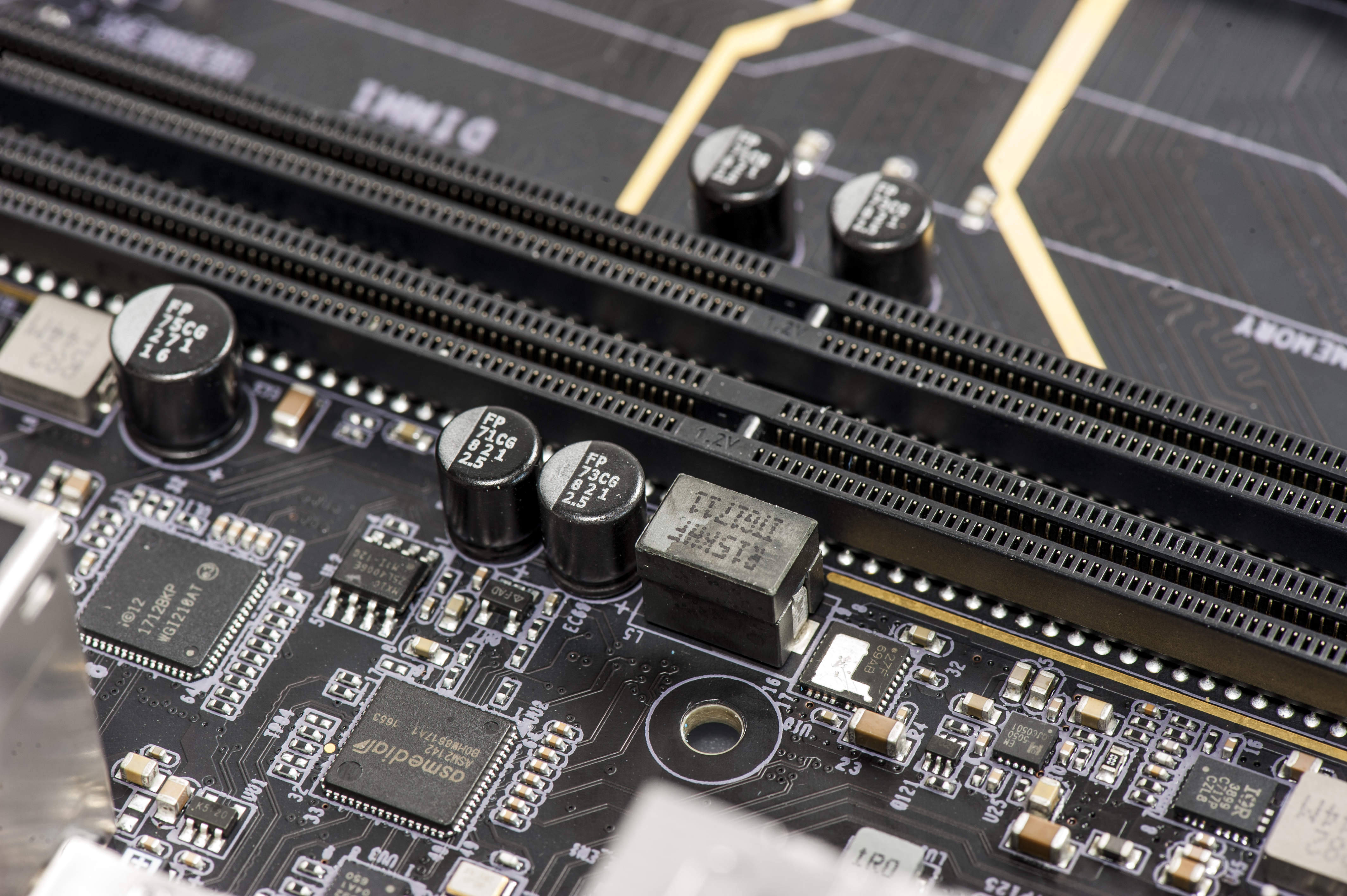

Image 31: Memory slots power regulators and support circuitry.
Often missed by reviewers, quality and power handling ability of the phase design is what’s important, not just sheer amount of phases. It’s relatively easy to populate lot of phases, but quite difficult to make a high-efficiency powerful per-phase design. Making high-phase VRM efficient even more challenging, as conversion losses are also added with additional switching components. To improve efficiency on the every day aircooling usage scenarios, VRM is down-shifted to 8-phase operation, turning off additional phases. Difference in thermals can be quite significant, reaching 10-15 °C gap.
Traditional power IC have plastic epoxy package, which is not a great thermal conductor. Even with added heatsink, temperatures inside the package are not improved much. 70-80% of the heat flow into copper pads and PCB layers as a result. Intersil SPS use special exposed metal tops, allowing heat to be dissipated not just thru PCBA copper layers, but also directly to VRM heat-sink plate.
If you want to use non-stock VRM heatsink plate, make sure you install protective mylar over the top surface of power stage ICs, as top exposed metal pad is connected to output power node. Do not short these ICs to ground by direct contact with metal heatsinks.
VRM also has all types of safety protections in place, such as OCP, OVP, UVP, phase failure protection and OTP. Over-temperature protection activate on temperatures above +105 °C if VRM regulator cooling solution is insufficient. There are two levels of protection action, soft – CPU will be throttled by frequency in order to reduce temperatures and hard, when system immediately shutdown to avoid catastrophic failure and thermal runaway.
X299 DARK design had multiple prototypes to find the best mix of power capacity, thermals and overclocking performance, so production board you see on photos above implement all that as result. For education purposes here is image of one of these early Rev 0.0 prototypes, which never left the secret labs:
As you can notice, VRM cooling solution is less advanced, and overall layout is bit different as well. PCIe slots don’t have fancy metal shield on them, DIMM slots are closer to the CPU and there are some extra debug ports and components present on this board to aid the development process. This board was made for initial testing around July-August 2017.
Voltage tuning functionality
All available voltages on this board are fully adjustable from BIOS or EVGA software tools. BIOS also optimized to adjust key settings automatically in user friendly mode, when only CPU ratio, XMP profile or memory settings are changed, so system still remain operational and stable, even if you forget to adjust critical voltage rail manually.
For voltage monitoring purposes this board also equipped with traditional EVGA ProbeIt connector, which is a 10-pin 2mm pitch PH-type connector near the top PCB edge.

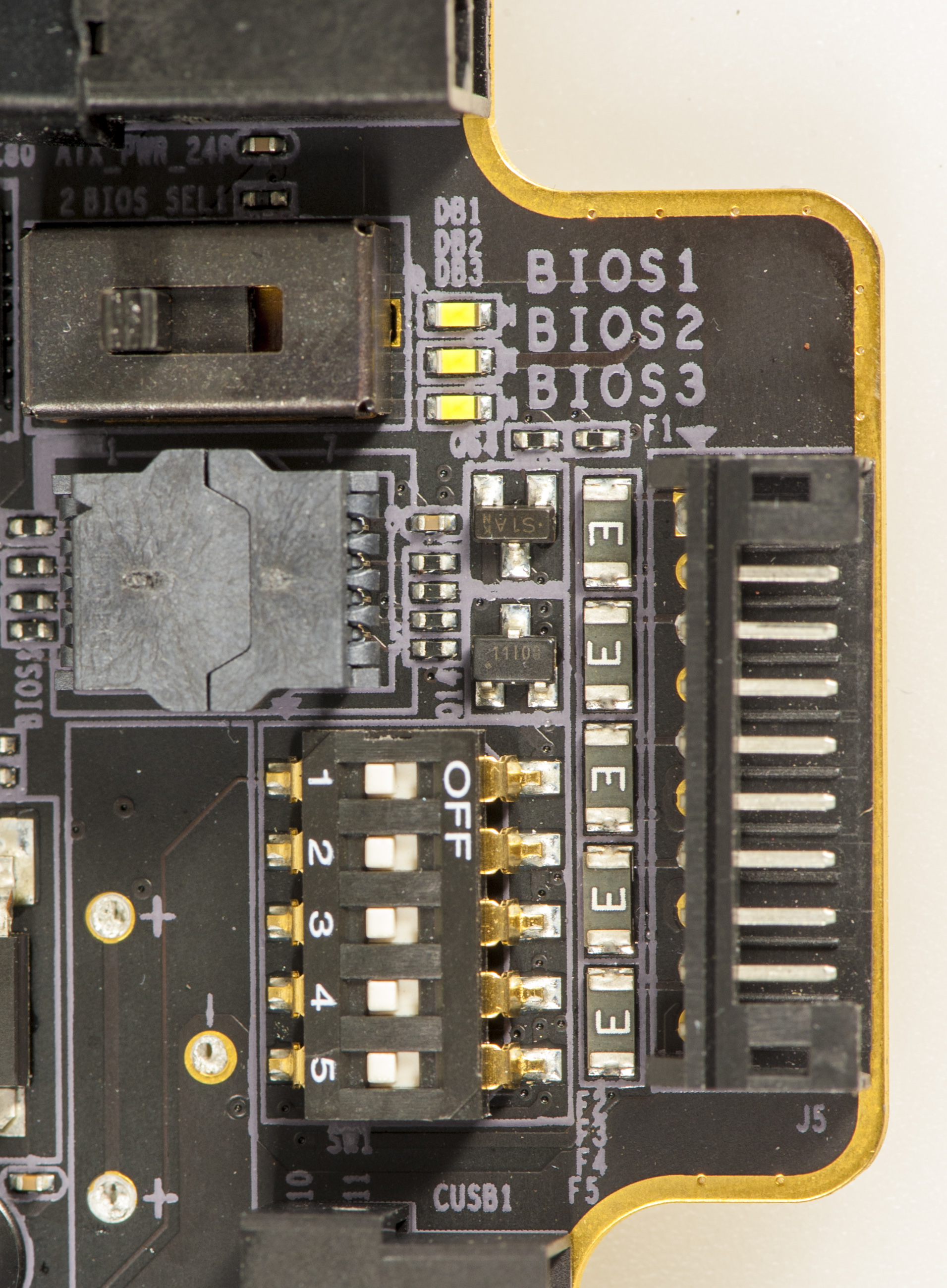
Image 32-33: Multifunction 80Port LED display, power/reset buttons, diagnostic LEDs, BIOS socket, switch and ProbeIt.
Pin definition as below:
| Pin 1 | CPU Vcore (KBX) or VCCIN (SKX) voltage |
| Pin 2 | Ground |
| Pin 3 | DIMM3/DIMM4 voltage |
| Pin 4 | Ground |
| Pin 5 | VCCPLL (KBX) voltage |
| Pin 6 | Ground |
| Pin 7 | System Agent (VSA) voltage |
| Pin 8 | Ground |
| Pin 9 | VCCPLL_OC (KBX) voltage |
| Pin 10 | Ground |
Table 3: ProbeIt measurement port pinout definition
This pinout is similar to one used on EVGA hi-end graphic cards since GTX 680 Classified, so you still can use your ProbeIt setup if you had it done before.
You can use bundled ProbeIt adapter to your usual multimeter probes, or in case you want to have custom cable connection to your specific meter, you can grab connector separately for example here from Digikey.com . You will also need these contacts. If you want less pins (for example only 4 to monitor VCORE and VDIMM voltage) you can get needed housings right here .
Realtime voltage monitoring
X299 DARK also has thruhole in center of CPU socket cavity to get physical access to processor backside when it is installed in the socket. This could be handy for precise temperature measurement and advanced CPU voltage probing at package capacitors. Please note, if you attach thermocouple to processor package, make sure metal thermocouple does not short any capacitor pads, otherwise you may damage the processor and/or board.
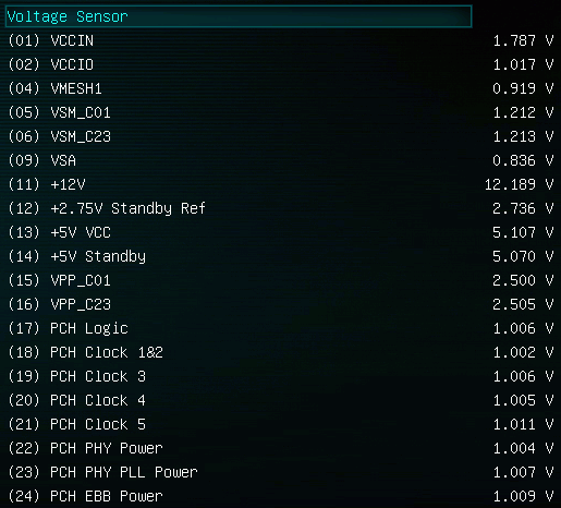
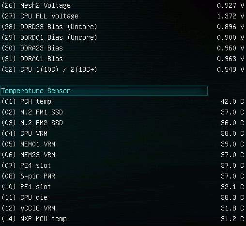
Image 34-35: Multifunction sensors available to display and monitor
LED Diagnostic indicators
Unlike most of modern average gamer boards, X299 DARK does NOT feature flashy RGB LEDs. It is styled in a monothonic black and metal gold theme. More to it, DARK mode allows to disable every single LED, no matter what the function of the LED is. That also include 80Port 7-segment diagnostics display.
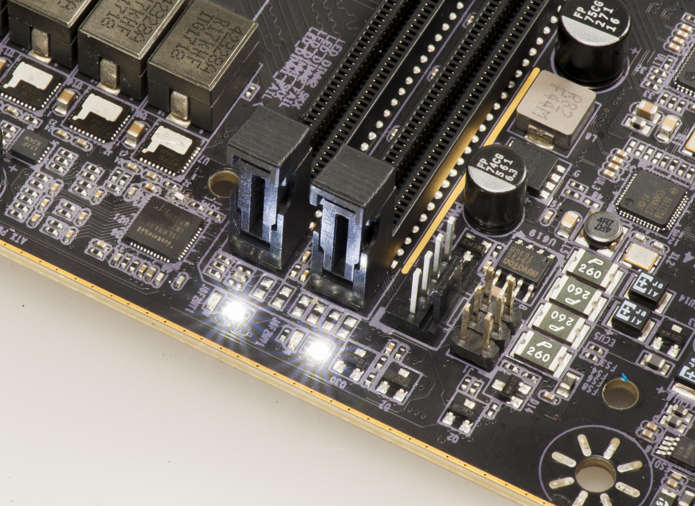
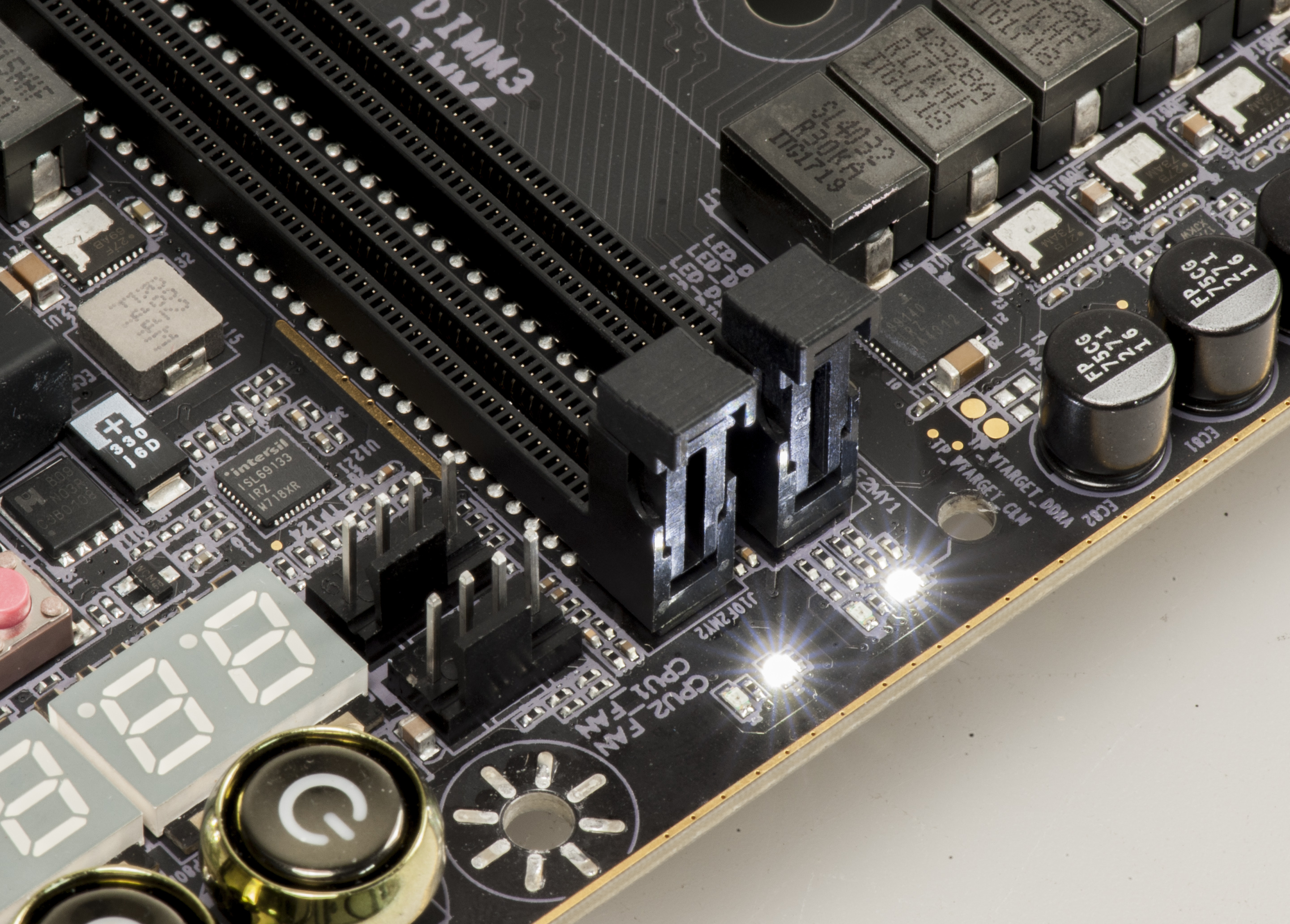
Image 36-37: DIMM status LED, dedicated to each specific slot.
DIMM and PCIe status indicators are handy during the initial POST and system assembly. Each PCIe and DIMM slots have their own LED near the latch to indicate if the slot is enabled and available to use with currently installed CPU. There are many possible lane mapping options depending on the installed CPU. Figuring out the specific system configuration is easy on DARK board even without reading the manual and digging into BIOS settings.
PCIe device mapping
All slots are fully compatible with all current PCIe speeds, such as Gen 1 (2.5 GT/s), Gen 2 (5 GT/s) and Gen 3 (8 GT/s). Intel’s X299 platform and Skylake-X/CascadeLake-X processors does not support PCI-Express Gen 4 (16 GT/s) speeds. Any device that is Gen 4 compatible will be operated at maximum Gen 3 speed.
| X299 DARK map | PE1 ×16/x8 | PE2 ×8 | PE3 ×8 | PE4 ×16/x8 | PE5 ×4 | PE6 ×4/x8 | PM1 | PM2 | PU1 | PU2 |
|---|---|---|---|---|---|---|---|---|---|---|
| Kabylake-X, 1 x GPU | x16 | No use | No use | No use | x4 PCH | x4 PCH | No use | No use | No use | No use |
| Kabylake-X, 2 x GPU | x8 | x8 | No use | No use | x4 PCH | x4 PCH | No use | No use | No use | No use |
| Kabylake-X, 2 x NVMe | No use | x8 | No use | No use | x4 PCH | No use | x4 or PU1 | x4 PCH | x4 or PM1 | No use |
| Skylake-X i7 2 x SLI | x16 | No use | No use | x8 | x4 PCH | x4 PCH | x4 CPU or PU1 | x4 PCH | x4 CPU or PM1 | No use |
| Skylake-X i7 3 x SLI | x8 | x8 | No use | x8 | x4 PCH | x4 PCH | x4 CPU or PU1 | x4 PCH | x4 CPU or PM1 | No use |
| Skylake-X i7 4 x GPU | x8 | x8 | No use | x8 | x4 PCH | x4 PCH | x4 CPU or PU1 | x4 PCH | x4 CPU or PM1 | No use |
| Skylake-X / CascadeLake-X i9 3 x SLI | x16 | No use | No use | x16 | x4 PCH | x8 CPU | x4 CPU or PU1 | x4 PCH | x4 CPU or PM1 | No use |
| Skylake-X / CascadeLake-X i9 3 x SLI | x16 | No use | x8 | x8 | x4 PCH | x8 CPU | x4 CPU or PU1 | x4 PCH | x4 CPU or PM1 | No use |
| Skylake-X / CascadeLake-X i9 4 x SLI | x8 | x8 | No use | x16 | x4 PCH | x8 CPU | x4 CPU or PU1 | x4 PCH | x4 CPU or PM1 | No use |
| Skylake-X / CascadeLake-X i9 5 x GPU | x8 | x8 | x8 | x8 | x4 PCH | x8 CPU | x4 CPU or PU1 | x4 PCH | x4 CPU or PM1 | No use |
| Skylake-X / CascadeLake-X i9 3 x NVMe | x16 | No use | No use | x8 | x4 PCH | No use | x4 CPU or PU1 | x4 CPU | x4 CPU or PM1 | x4 CPU |
Table 4: X299 DARK PCIe mapping between slots
CascadeLake-X 10xxx series processors have 48 lanes, but additional four lanes are not routed/not used on EVGA X299 DARK. As result PCIe mapping on these processors are exactly same as 44-lane Skylake-X chips.
Slots designated for dual-spacing devices, such as graphics cards have additional metal shields for improved mechanical support. Intel® Optane™ memory module can be used only on PM2 M.2 slot, with both CPUs.
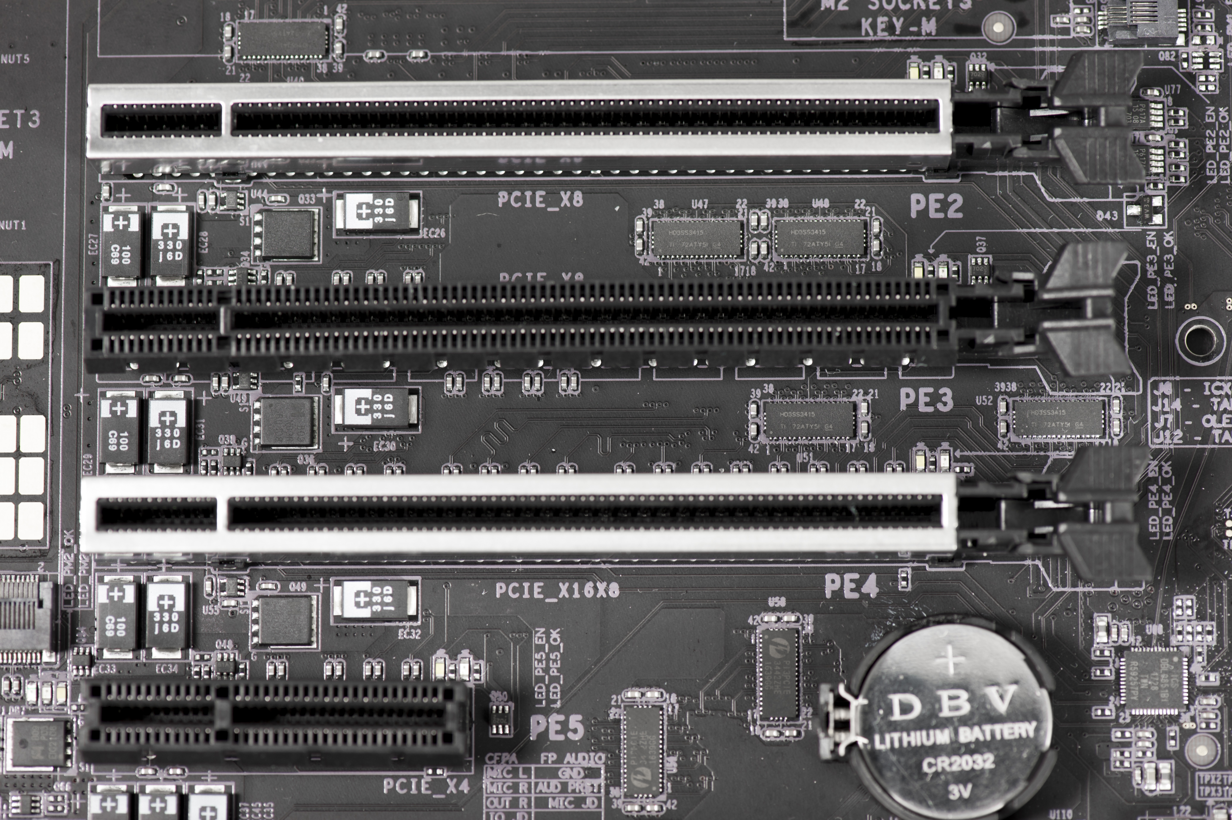
Image 38: PCIe slots routing and mechanical.
NVMe support
By removing airduct M.2 cooler cover user can get access to the high-speed storage slots. Pair of NVMe slots have M.2 form-factor and support any PCIe-based SSD devices. Left PM2 slot also supports Intel Optane Memory modules.


Image 39-40: M.2 cooler cover removed and Samsung 960 Pro NVMe drive installed in PM1 slot.
Also DARK supports Intel VROC for enterprise storage-demanding applications, allowing multiple NVMe SSD arrays to be build using CPU-attached PCIe Gen3 lanes. VROC require paid Intel HW key, that plugs into the dedicated connector VROC_WAFER on the board. VROC key is required for support of Bootable RAID 0/1/5/10 using existing Intel NVMe-based SSD.
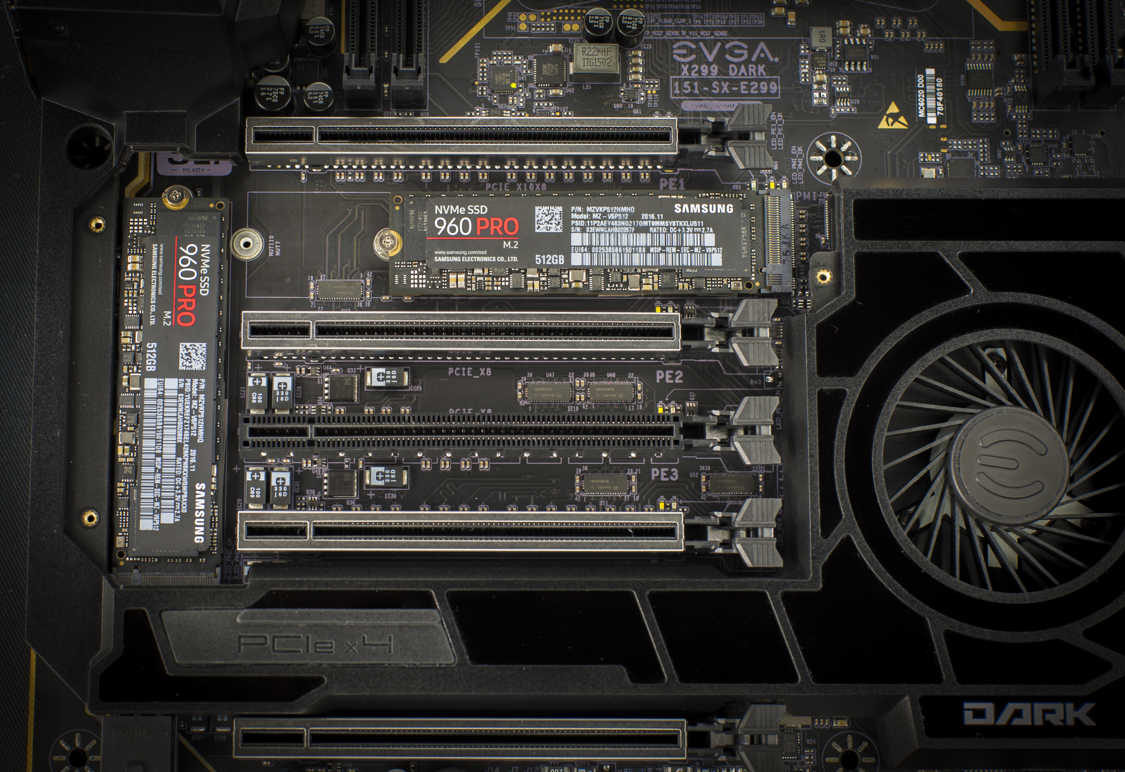
Image 41: Both Samsung 960 Pro NVMe installed on both PM1, PM2 slots.
VROC keys have two tiers, Standard and Premium. At the moment of writing VROC is supported by Windows 7 SP2, Windows 10, Windows 2012 R2, Windows 2016, RHEL 7.3 and SUSE Linux Enterprise 12 SP3. Standard key allow use of VROC with Samsung SM951, SM961, PM953, PM961, Toshiba XG3, Micron 9100, Lenovo Atsani and Huawei ES3600P NVMe drives and allow up to 24 SSD.
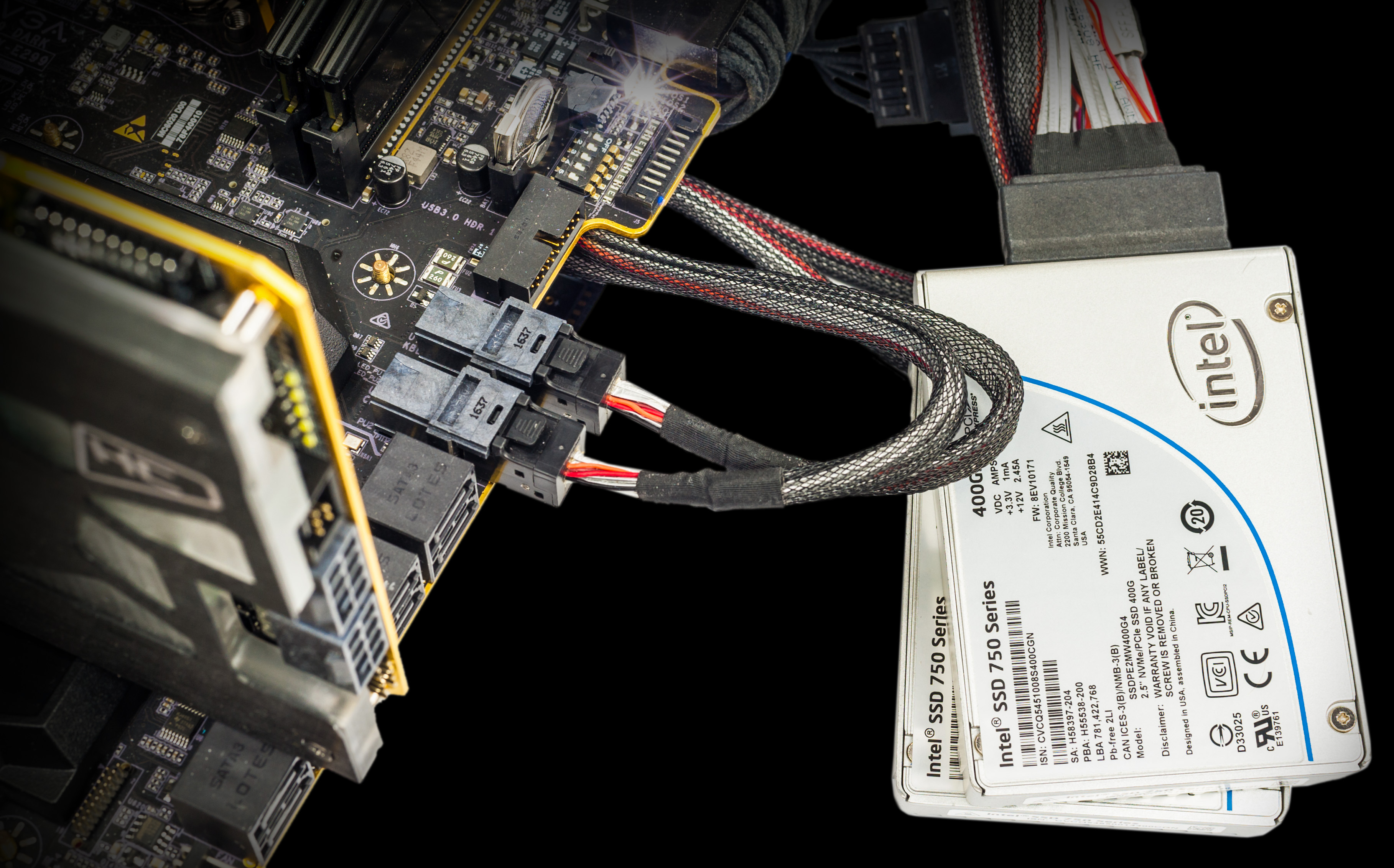
Image 42: Pair of Intel 750 NVMe SSDs connected to X299 DARK U.2 ports
All these multi-SSD options are available when using PCIe-M.2 adapters that allow operation of multiple M.2 SSDs in single x16 port. It’s important to keep SSD array within one PCIe root complex, meaning that essentially there are “only” 11 NVMe drives can be used on X299 DARK:
- First array of 4 drives installed into PE1 ×16 slot
- Second array of 4 drives installed into PE4 ×16 slot
- 2 more drives installed in PE6 (or 1 PCIe drive with 1 U.2 PU2 drive).
- Last drive installed either in PM1 or PU1 port.
This requires Core i9 44-lane processor to be fully functional. Total bandwidth of such an insanely expensive storage system would reach 352 Gbit/s, or 44 GBytes/s, if all drives are configured and working at PCIe Gen3 ×4 speed.

Image 43: Close-up of M.2 PM1 card connector, Socket Type 3, Key M.
Board also supports the new 3D-Xpoint SSD drives, such as Intel® Optane™ SSD 905P, older Optane™ SSD 900P, Optane™ SSD DC P4800X and M.2 110mm Optane™ SSD DC P4801X
Onboard controllers
Board features a variety of proven controllers to provide additional connectivity. Two RJ45 LAN connectors powered by Intel Network controllers (i219V PHY and i210AT MAC) support speeds up to 1Gbps and have support for speed/redundancy teaming.
Pair of USB 3.1 10Gbps ports connected to ASMedia ASM2142 + ASM1543 combo. This controller connected to two lanes of PCIe Gen3 from X299 PCH.
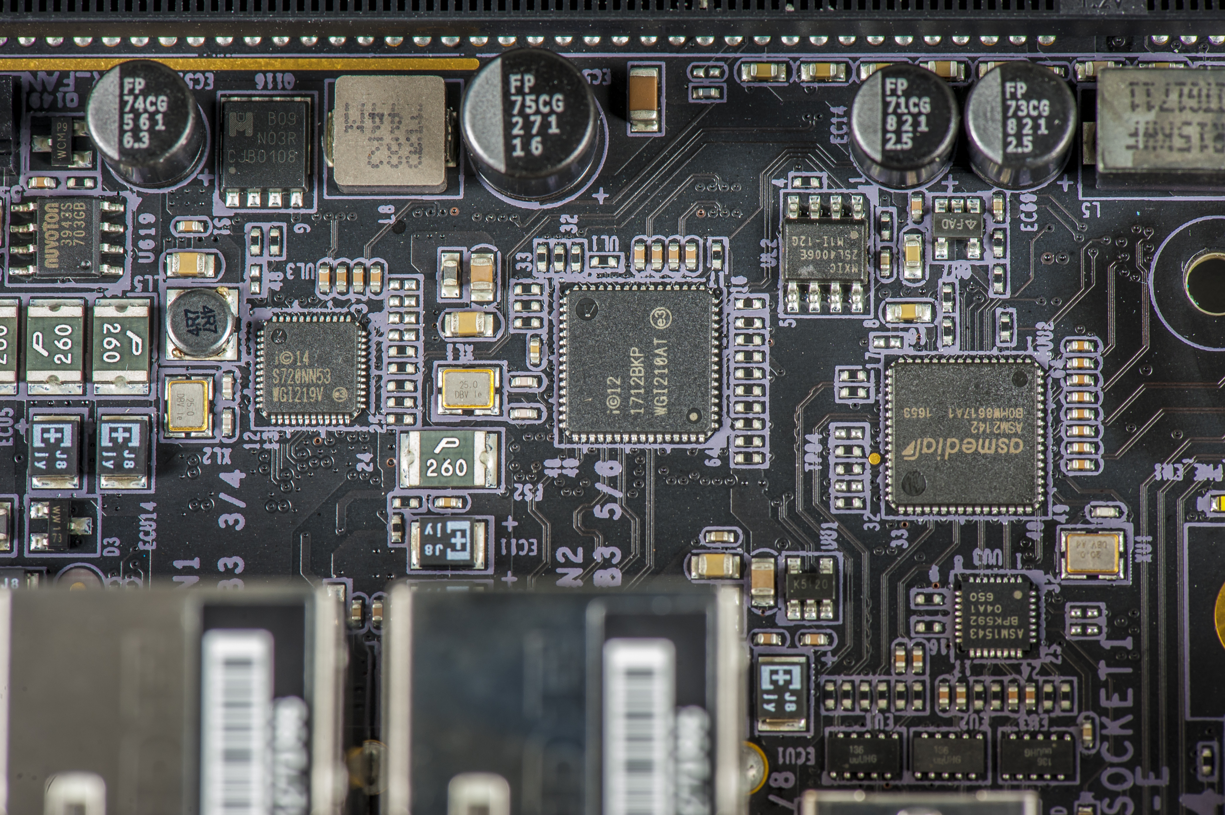
Image 44: Left to right: Intel i219V PHY, Intel i210-AT MAC, ASMedia ASM2142 USB 3.1 hub, ASM1543 Type-C Mux.
M.2 card format WiFi/Bluetooth module does not come with the board in retail package, but slot is there ready for it.
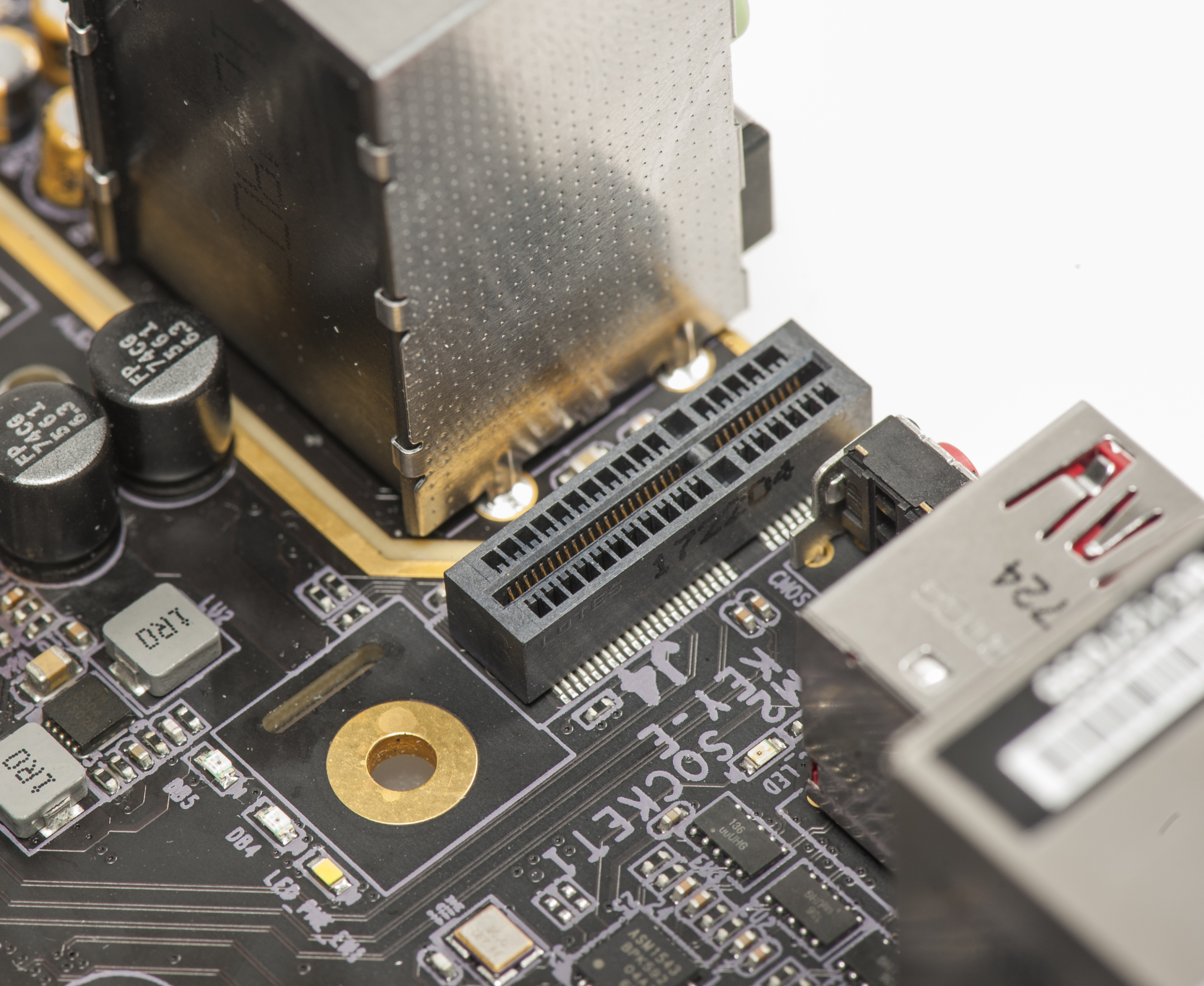
Image 45: Socket Type 1 Key E socket for WiFi/BT card.
Demanding content producers and multimedia enthusiasts may find multi-channel Creative Sound Core3D solution beneficial for accurate sound processing. This sound chipset supports most of traditional Creative X-Fi features. Digital SPDIF is also supported via optical port.
Image 46 shows a little provision for bottom side audio separation LED backlight, but in retail configuration none of that is populated, as light would be blocked by the board cover airduct. anyway :). Case modders anyone?
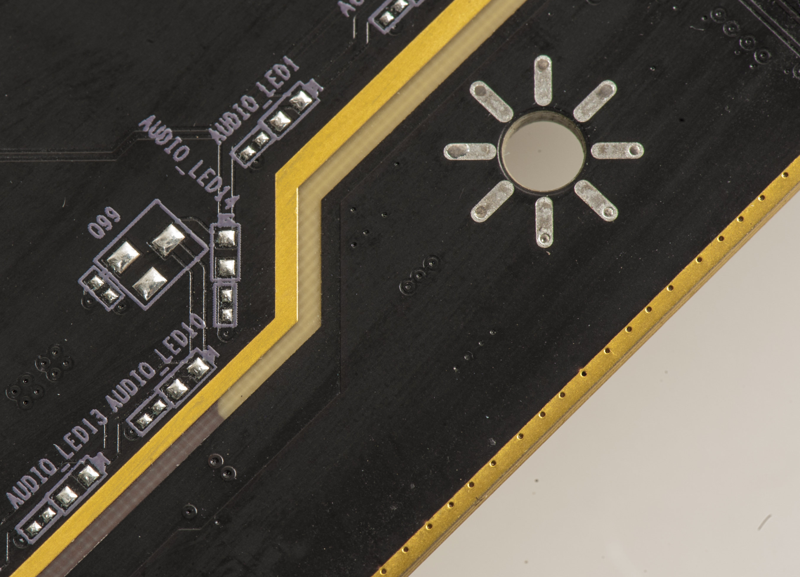
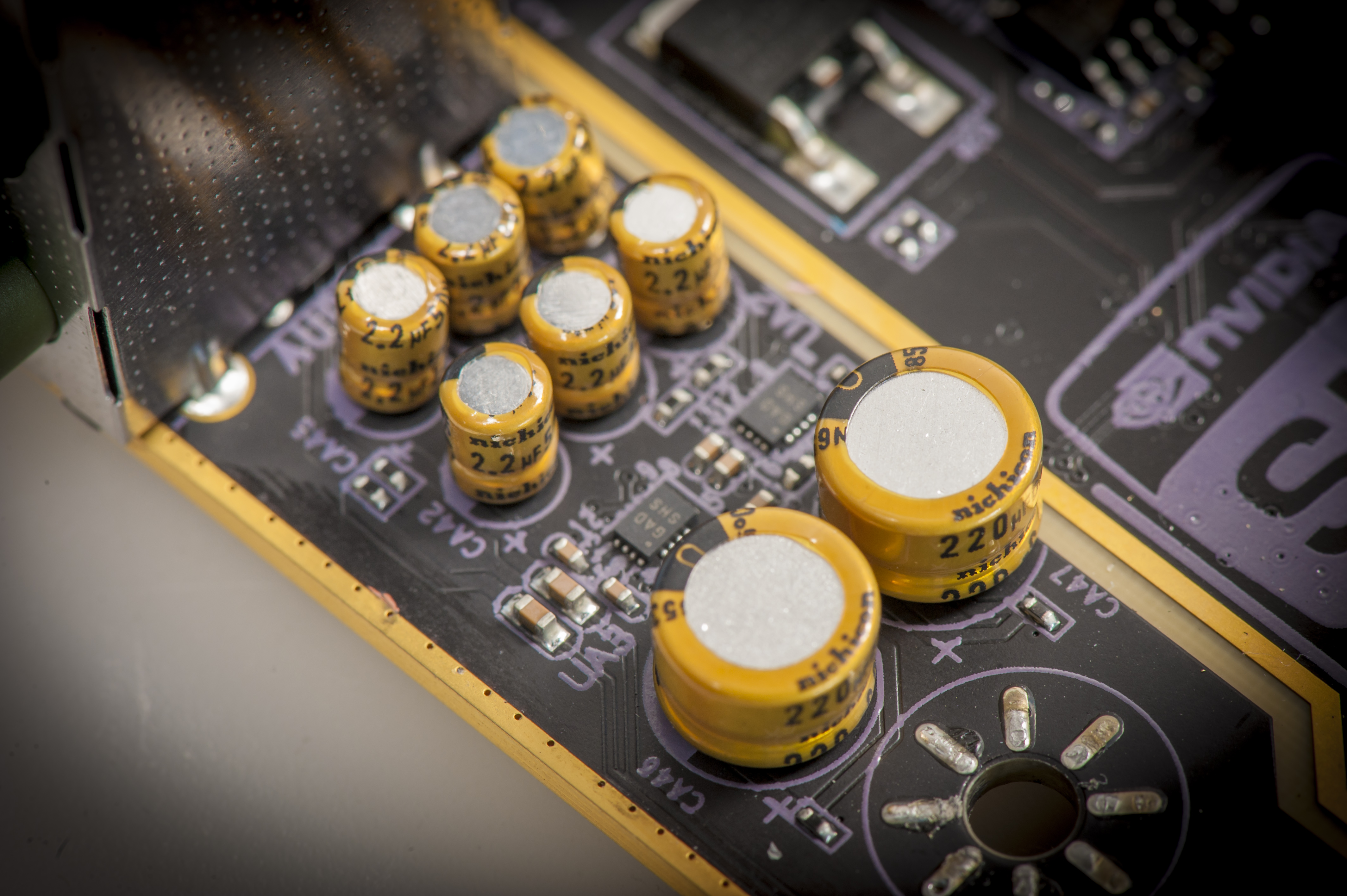
Image 46-47: Unpopulated audio LED option and Nichicon gold series capacitors for audio AC coupling.
Audio chipset linked to PCH thru dedicated interface, so audio functionality is not affected by overclocking.
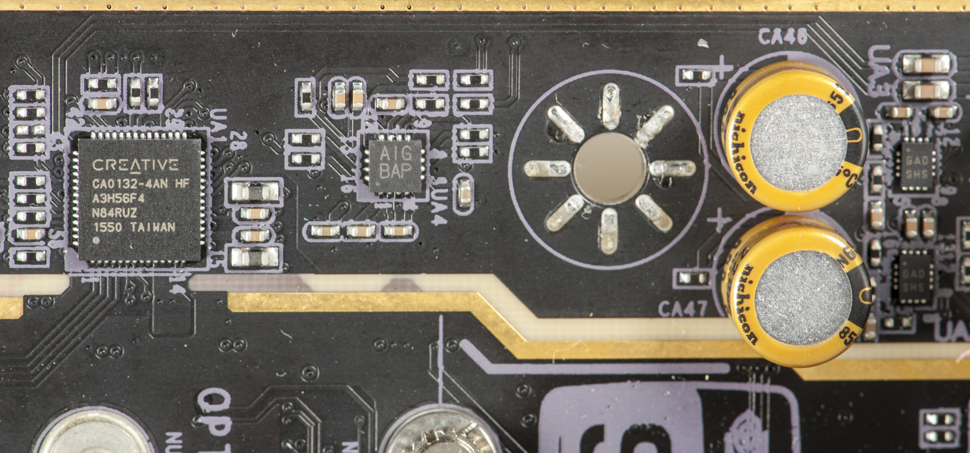
Image 48: Creative Sound Core3D™ Audio DSP circuitry
Legacy OS support
Board is friendly for old operation systems, like Windows XP or Windows Vista, thanks to legacy ASMedia ASM1061 SATA controller and PS/2 keyboard port.
Fan/pump headers
All fan headers able to support medium power fans and pumps, with supply up to +12V and working current up to 2 Amp. There are 7 fan headers, each of which are 4-pin type with PWM signal.
- CPU1_FAN – Main processor fan/pump header
- CPU2_FAN – Secondary processor fan/pump header
- CHA_FAN – Chassis fan located near SATA 4/5 connector
- SYS1_FAN – First system fan, right next to CHA_FAN
- SYS2_FAN – Second system fan, near chassis button/LED header
- PWR_FAN – VCORE VRM cooling fan header in top left corner
- Special 4-pin PCH_FAN located next to SYS2_FAN, dedicated to onboard PCH fansink.
There is also secret IO_FAN, hidden under the I/O cover.
Right-angle connectors
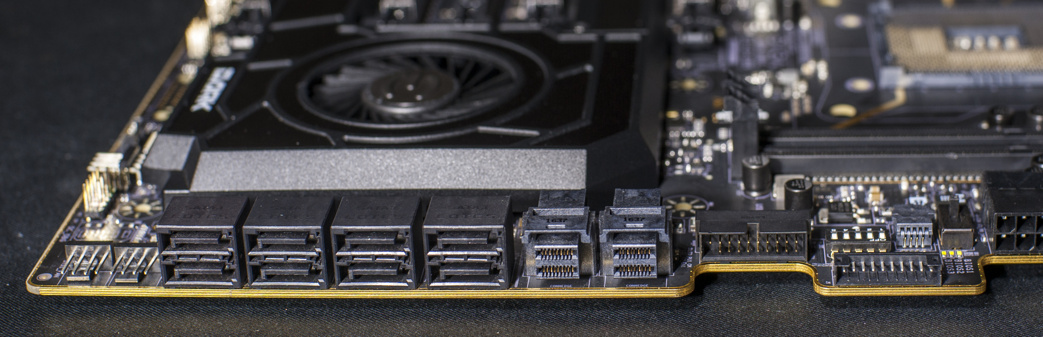
Image 49: Inside board edge side with SATA/NVMe and right angle connectors.
PCH SATA controller support two operation modes, AHCI and RAID. In either mode, controller compliant to SATA Specification, Rev3.2 and provide transfer speeds up to 6 Gbps on each available port.
Intel® Rapid Storage Technology (RST) is also provided for management and RAID functionality. RAID arrays with up to SIX devices can be built (using ports SATA 0 to SATA 5). PCH SATA ports support four levels of RAID arrays:
- RAID 0 : Stripe, reduced fault tolerance (any drive failure will cause array failure).
- RAID 1 : Mirror, copy data to multiple drives (all drives in array are exact copy).
- RAID 5 : Stripe with parity (all drives contain parity blocks to tolerate loss of one drive).
- RAID 10: Nested RAID 1 + RAID 0 array for better failure resilence and speed.
Individual USB protection
Each USB port available on the board is rigorously protected from ESD and EMI to improve interface reliability and uninterrupted operation. Also overcurrent protection for each USB jack is handled independently, so even if your connected device draw too much current, only the affected port will be disabled, leaving other devices operation unaffected.
SLI support
Board supports NVIDIA SLI multi-GPU operation with both CPU types. However with Kabylake-X due to limited amount of PCIe lanes available, only 2-way configuration is possible, using two top PCIe slots, PE1 and PE2. In this case U.2 NVMe interfaces will be disabled. Only options for NVMe SSD in SLI configuration would be lanes routed from PCH to PM2 M.2 socket or last PE6 PCIe mechanical slot. PCI-express slot PE5 with fixed x4 width slot is always active, powered by PCH lanes.
With Skylake-X i7 CPUs configurations up to 3-way are possible and top-tier i9 CPUs allow most flexibility with support up to 4-way.
Slots PE1 and PE4 have ability to run at full x16 lane width, which provide fastest graphics in 2-way SLI mode. Adding PCIe device to PE2 or PE3 will degrade width to x8. X299 DARK layout with such setup leaves PE6 for SSD or network card.
Multifunction 80Port LED display
Four-digit 7-segment LED display in visible top right corner of the board enables prompt diagnostics of possible overclocking issues and system errors. It displays standard 80h POST diagnostic codes like the typical enthusiast board, but also capable to show readout of multiple onboard temperature sensors and calibrated hardware voltage sensors. Together with onboard slot LEDs user often can quickly find out configuration problem even without having monitor attached to the system.
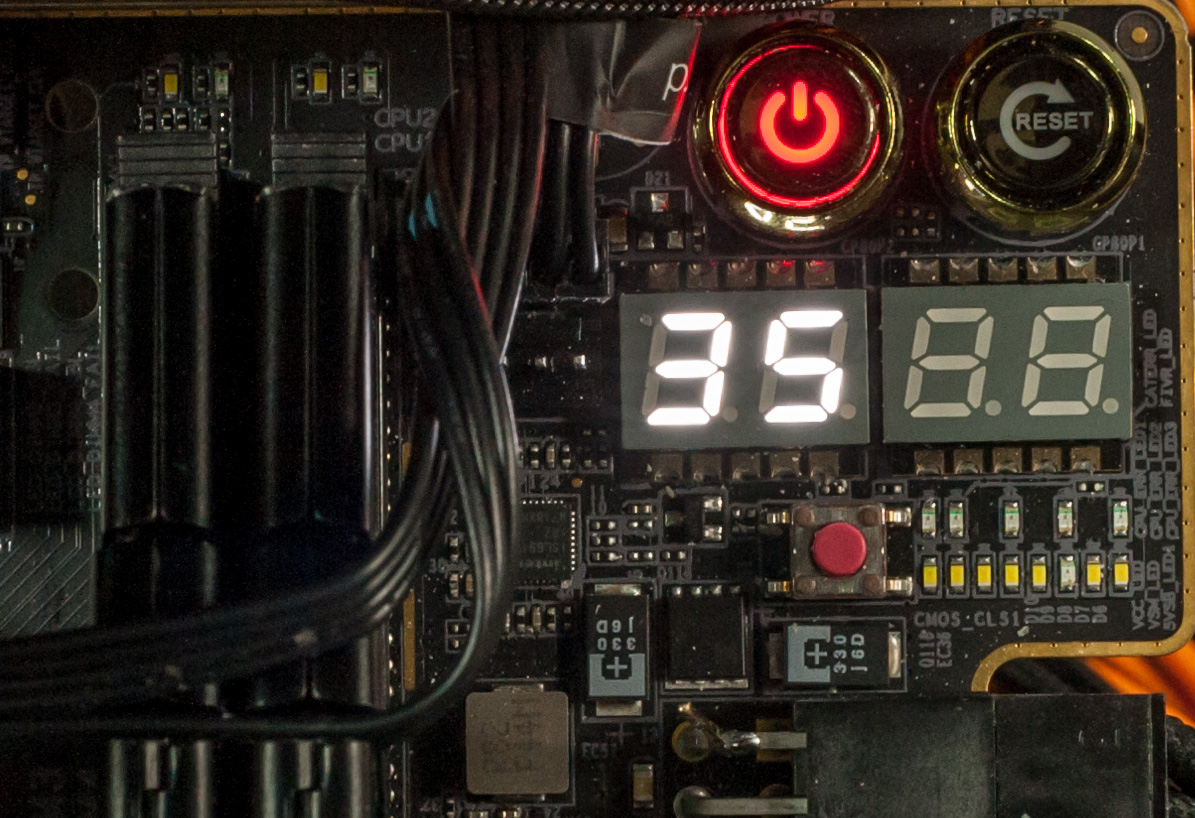

Image 50-51: Standard 80h POST code display with DARK mode (no auxilary LEDs) enabled and hardware monitoring readout.
Memory error POST codes, such as 55 or E8 together with dedicated per-slot white/red status LEDs narrow down issue to specific memory channel/module. CPU errors also indicated by RED CATERR_LED near Clear CMOS button. During normal stable operation red CATERR_LED should be never lit.
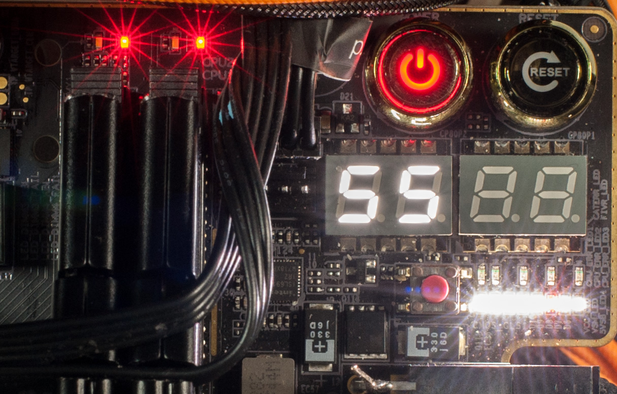
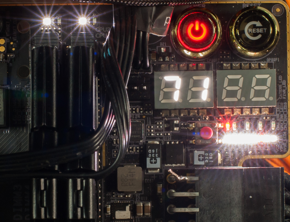
Image 52-53: Failed memory overclocking trigger 55 POST code and two DIMM LEDs turn RED. CATERR_LED for CPU errors.
Some typical error codes that may be caused by unstable components / overclocking:
| 80Port code | Description and possible reason |
|---|---|
| C | CPU/MB cannot operate. Can also be caused by missing +12V power or water condensation |
| FF | CPU cannot initialize, too high CPU or BCLK clock. Can also be caused by power issue or too cold temperature. |
| b0 | Memory cannot train requested speed/timings. Can be also caused by damaged DDR4 module or bent socket pin. |
| b3 | Memory SPD data is not correct. Can be also caused by damaged DDR4 module or bent socket pin. |
| b7 | Memory cannot train requested speed/timings. Can be also caused by damaged DDR4 module or bent socket pin. |
| 55 | Memory is not detected. Problem with DDR4 or CPU memory controller, can be caused by too high clock/timings. |
| E8 | Memory is not detected. Problem with DDR4 or CPU memory controller, can be caused by too high clock/timings. |
| 71 | System hang due to Kabylake-X CPU overclocking instability. |
| d6 | PCIe graphics card is not detected, no display. Problem with VGA card or VGA BIOS |
| d7 | Keyboard is not detected. Problem with USB or PS/2 keyboard |
Table 5: Typical 80Port error codes during overclocking and system troubleshooting.
Diagnostic display, just like all other LEDs can be also completely disabled to create true DARK motherboard, without a single point of LED light.
This 80Port display on DARK series motherboards also can display various onboard sensors, including temperature with range down to -64 °C. While own CPU reporting sensor cannot read anything below -4 °C, X299 DARK have special hardware to overcome that limitation, so this can be very useful to check good thermal contact when benching with dry ice (-74 °C min temp) or phase-change/chiller systems (about -20 to -40 °C).
Software for X299 DARK overclocking
EVGA have own tuning utility for all motherboard series, called ELEET.
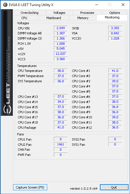
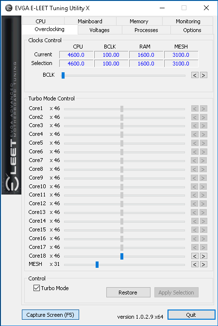
Image 54-55: ELEET Utility HW monitoring and OC control tabs.
EVGA X299 DARK advanced sensor monitoring functionality also fully supported by HWiNFO monitoring software starting from Build 3390.
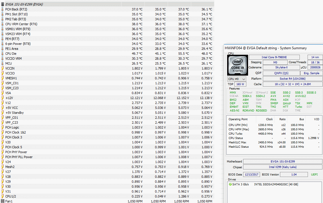
Image: HWiNFO monitoring tool showing all EVGA X299 DARK sensors.
BIOS & Tools
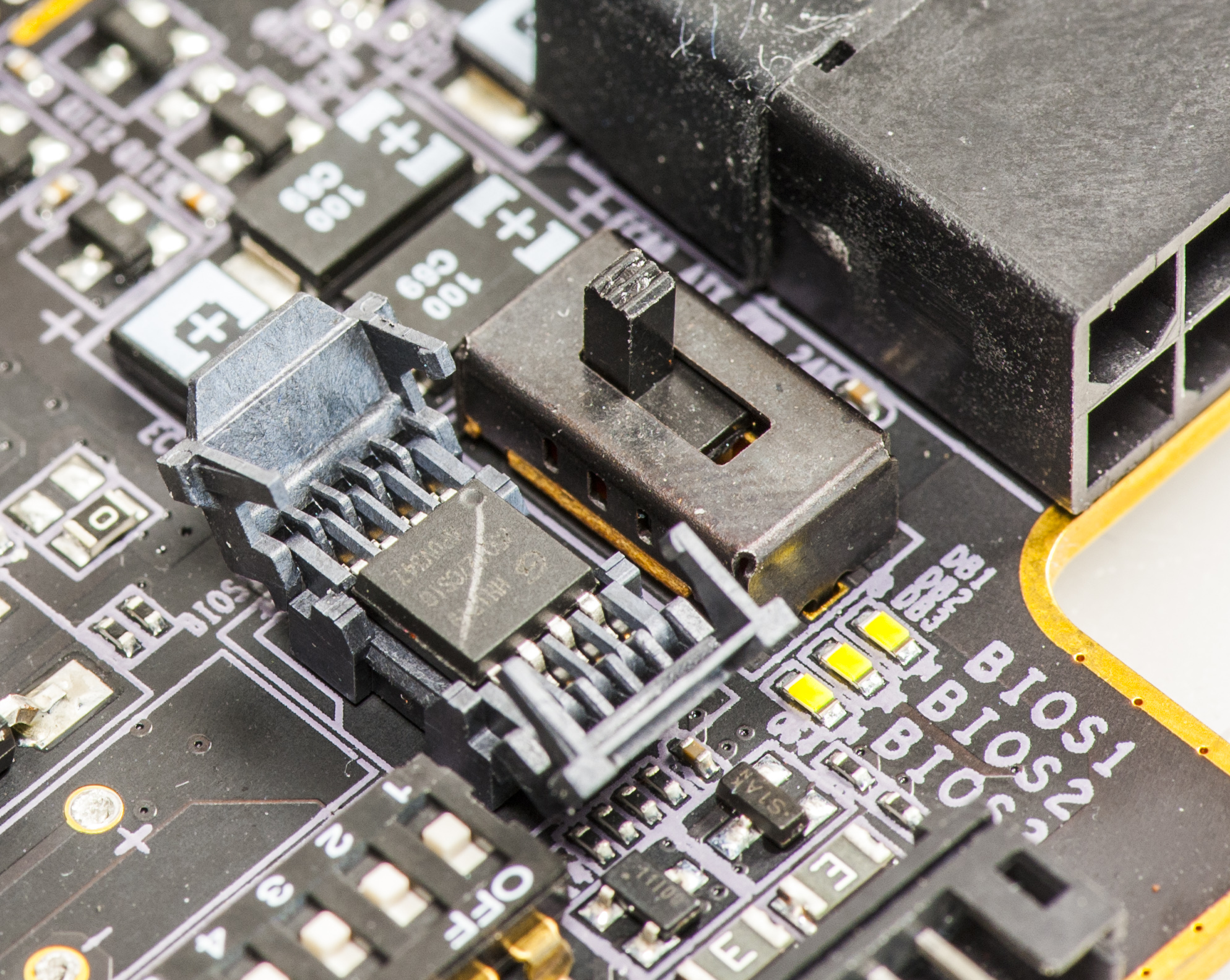
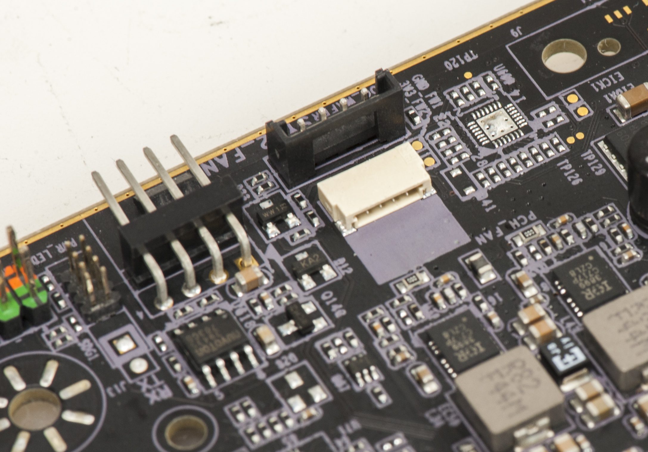
Image 56-57: BIOS1 chip socket and BIOS switch, SYS2_FAN and PCH fan headers.
BIOSes in this section are compatible only with EVGA X299 DARK board and will not work and may damage any other motherboard on attempt to flash.
EVGA X299 DARK board has three different BIOS ROMs and corresponding switch near 24-pin ATX power connector to select between them. All three BIOS ROMs from factory are equal, and functionally same. Using multiple BIOS chips allow user to freely experiment with overclocking, without risk of BIOS corruption. Also user may utilize one BIOS ROM for overclocking, and keep other BIOSes for every day gaming or regular use.
| BIOS mode LED indicator | BIOS1 | BIOS2 | BIOS3 |
|---|---|---|---|
| BIOS location | Removable, IC socket | Fixed onboard | |
| BIOS Version | v1.00 | ||
| PCH Fan profile | Auto | ||
| CPU Support | Skylake-X and Kaby Lake-X, all CPUs | ||
| Extreme OC ready | Yes | ||
Table 6: BIOS ROMs on the board.
BIOS ROM and flash tool, Ver.1.00 for EVGA X299 DARK
BIOS ROM and flash tool, Ver.1.01 for EVGA X299 DARK
BIOS ROM and flash tool, Ver.1.02 for EVGA X299 DARK
BIOS ROM and flash tool, Ver.1.03 for EVGA X299 DARK
BIOS ROM and flash tool, Ver.1.04 for EVGA X299 DARK
BIOS ROM and flash tool, Ver.1.05 for EVGA X299 DARK
BIOS ROM and flash tool, Ver.1.06 for EVGA X299 DARK
BIOS ROM and flash tool, Ver.1.07 for EVGA X299 DARK
BIOS ROM and flash tool, Ver.1.08 for EVGA X299 DARK
BIOS ROM and flash tool, Ver.1.09 for EVGA X299 DARK
BIOS ROM and flash tool, Ver.1.12 for EVGA X299 DARK
BIOS ROM and flash tool, Ver.1.14 for EVGA X299 DARK
BIOS ROM and flash tool, Ver.1.17 for EVGA X299 DARK
BIOS ROM and flash tool, Ver.1.18 for EVGA X299 DARK
BIOS ROM and flash tool, Ver.1.19 for EVGA X299 DARK
BIOS ROM and flash tool, Ver.1.20 for EVGA X299 DARK
BIOS ROM and flash tool, Ver.1.21 for EVGA X299 DARK
BIOS ROM and flash tool, Ver.1.23 for EVGA X299 DARK
BIOS ROM and flash tool, Ver.1.26 for EVGA X299 DARK
BIOS versions 1.10, 1.11, 1.13, 1.22 are internal test builds only and not released to public. Skylake-X Refresh CPUs are fully supported starting from Ver 1.12, but will boot even with older BIOSes. CascadeLake-X fully supported starting from Ver 1.23, and initial support added since Ver 1.19.
BIOS 1.17 fixes PCIe 28/44-lane detection issue with Intel i7-9800X CPU.
CascadeLake-X processors require BIOS Ver.1.19 or newer.
BIOS Ver.1.26 supports resizeable BAR.
Custom BIOS
Currently everything ever needed for OC is already implemented in production release BIOS versions, so no custom BIOS ROM images required for aircooling/watercooling OC.
If you interested in extreme overclocking (that is using chillers, phase-change coolers, Dry Ice or Liquid Nitrogen), then special BIOS builds from links below can help to push OC further.
XOC BIOSes from this section provided AS IS and no official warranty or support are available.
We spend great effort to make sure board overclocks great on LN2, but do not validate all other functionality for these custom builds.
XOC BIOS is NOT secure against Spectre/Meltdown attack!
Luumi have tested i9-10980XE CascadeLake-X LN2 overclocking with EVGA X299 DARK XOC BIOS. Here’s the image that he used for the test.
XOC BIOS ROM and flash tool, Ver.X05 for EVGA X299 DARK
Changeset for X05 version:
- Supports CascadeLake-X processors
XOC BIOS ROM and flash tool, Ver.X04 for EVGA X299 DARK
This XOC BIOS is NOT compatible with latest Intel CascadeLake-X processors (109xx series chips). System will hang on post code 0xDF in such case.
Changeset for X04 version:
- Improved memory overclocking and memory training performance
- Added memory round trip and I/O latency settings in BIOS Setup (RTL/IO)
- Default timings are optimized for better compatibility
- This BIOS is NOT patched for CVE-2017-5753, CVE-2017-5715 and CVE-2017-5754 security issues
XOC BIOS ROM and flash tool, Ver.X03 for EVGA X299 DARK
This XOC BIOS is NOT compatible with latest Intel CascadeLake-X processors (109xx series chips). System will hang on post code 0xDF in such case.
Changeset for X03 version:
- Unlocked VCCIO voltage range for higher ring overclocking. (BIOS versions 1.09 and newer already have this patch).
- Max memory voltage limit is increased to 2.30 V. (BIOS versions 1.09 and newer already have this patch).
- Memory performance and training is improved. (BIOS versions 1.09 and newer already have this patch).
- This BIOS is NOT patched for CVE-2017-5753, CVE-2017-5715 and CVE-2017-5754 security issues
To avoid confusion with normal BIOS image, these archives are password protected. Password is E299_DARK. This is just small simple step, to check if you read this section, and accept all and any possible the risks.
Do NOT use ELEET X tool for voltage control on X299 DARK. It will likely cause system to crash and lock. Best way is to set all voltages in BIOS and use windows software to control CPU/Mesh ratio during overclocking session. Intel XTU also works for CPU ratio adjustments.
BIOS overview and control items detail
EVGA GUI BIOS is based on AMI UEFI codebase and optimized for fast and easy control over all motherboard settings. BIOS supports all common features, like USB-key update, screenshot to USB capture, saving and loading settings up to 16 profiles and storing profiles to USB drive.
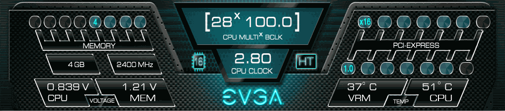
Image 58: BIOS GUI top status display.
Top overview section shows realtime health status. Left section provides information about detected memory amount, memory capacity and memory frequency. Actual CPU voltage and memory voltage is shown here on bottom left bar as well.
Right section shows current PCIe slot configuration, like detected PCIe device electrical width and speed generation. VRM temperature and CPU die temperatures are reported here as well.
Center block has a display for CPU Core ratio, actual BCLK and resulting CPU clock frequency. Little chip icon by the left side indicates amount of active cores (not including logical HT cores) and “HT” icon indicate activated Intel Hyper-Threading technology support.
Be sure to go and change the CPU TJMax value from Auto to +95 °C in the BIOS under CPU Configuration menu. The BIOS incorrectly sets TJMax to +105 °C if left at Auto. Intel Support team confirms that TJMax for Skylake-X should be kept at +95 °C. When CPU TJMax in the BIOS is set incorrectly ALL temperature monitoring applications that use DTS offsets will display the wrong CPU die temperature.
For major voltage control, like VCORE or VMESH there are two different modes of operation – Adaptive and Override. The default mode of operation is adaptive mode, so power management engine can adjust voltage, based on CPU utilization and running frequency. Override mode forces specific voltage to the CPU, ignoring any power state/frequency state changes. Both adaptive and override modes can be set separately and independently for each voltage (CORE, MESH). It is recommended to first test with Override mode, to find out limits of particular CPU at desired running frequency. Once you know relation between max clock and voltage, you can try to use Adaptive and tune settings to get automatic power management, while still providing enough voltage for CPU under max stress.
| Kabylake-X voltages | Normal mode | Extreme OC mode enabled | Intel stock default | |||
|---|---|---|---|---|---|---|
| Minimum … Maximum | Minimum … Maximum | |||||
| CPU VCORE Adaptive | ||||||
| Target Voltage | 1.20 … 1.50 V | 1.20 … 2.00 V | Per CPU VID | |||
| Offset Voltage | -500 … +300 mV | -500 … +500 mV | 0 mV | |||
| CPU VCORE Override | ||||||
| Target Voltage | 1.20 … 1.60 V | 1.20 … 2.00 V | Per CPU VID | |||
| VCCIN Vdroop | Enable | Disable | Auto | |||
| DIMM Voltage | 1.20 … 1.60 V | 1.20 … 2.00 V | 1.20 V | |||
| VSA Voltage | 0.80 … 1.40 V | 0.80 … 1.60 V | 1.05 V | |||
| VCCIO Voltage | 0.95 … 1.40 V | 0.95 … 1.80 V | 0.95 V | |||
| VCCPLL Voltage | 1.00 … 1.40 V | 1.00 … 2.00 V | 1.00 V | |||
| VCCPLL_OC(Overclocking PLL) Voltage | 1.20 … 1.60 V | 1.20 … 3.00 V | 1.20 V | |||
| Core PLL Voltage | 0.90 … 1.40 V | 0.90 … 1.85 V | 0.90 V | |||
| VCCST Voltage | 1.00 … 1.20 V | 1.00 … 1.60 V | 1.00 V | |||
| PCH Voltage | 1.00 … 1.20 V | 1.00 … 1.50 V | 1.00 V | |||
Table 7: Kabylake-X voltage controls available in BIOS.
Skylake-X processor does not have external VCCPLL, VCCPLL_OC voltages. It has Uncore offset, Vmesh offset and additional DIMM voltage for memory modules near I/O side of the board.
| Skylake-X voltages | Normal mode | Extreme OC mode enabled | Intel stock default | |||
|---|---|---|---|---|---|---|
| Minimum … Maximum | Minimum … Maximum | |||||
| VCCIN Voltage | 1.70 … 2.10 V | 1.70 … 2.60 V | 1.80 V | |||
| VCCIN Vdroop | Enable | Disable | ||||
| CPU VCORE Adaptive | ||||||
| Target Voltage | 1.20 … 1.50 V | 1.00 … 2.00 V | Per CPU VID | |||
| Offset Voltage | -500 … +300 mV | -500 … +500 mV | 0 mV | |||
| CPU VCORE Override | ||||||
| Target Voltage | 1.20 … 1.50 V | 1.00 … 2.00 V | Per CPU VID | |||
| CPU MESH Adaptive | ||||||
| Target Voltage | 0.90 … 1.40 V | 0.90 … 2.00 V | Per CPU VID | |||
| Offset Voltage | -500 … +300 mV | -500 … +500 mV | 0 mV | |||
| CPU VMESH Override | ||||||
| Target Voltage | 0.90 … 1.40 V | 0.90 … 2.00 V | Per CPU VID | |||
| Uncore Voltage Offset | 0 … +600 mV | 0 … +1000 mV | 0 mV | |||
| DIMM Voltage | 1.20 … 1.60 V | 1.20 … 2.00 V | 1.20 V | |||
| VSA Voltage | 0.80 … 1.40 V | 0.80 … 1.60 V | 0.80 V | |||
| VCCIO Voltage | 0.95 … 1.40 V | 0.95 … 1.80 V | 1.00 V | |||
| PCH Voltage | 1.00 … 1.20 V | 1.00 … 1.50 V | 1.00 V | |||
| PLLtrim Offset | -63 … +63 | -63 … +63 | 0 | |||
| MC(memory controller) PLLtrim Offset | -63 … +63 | -63 … +63 | 0 | |||
Table 8: Skylake-X voltage controls available in BIOS.
Also with Skylake-X you don’t need to worry about VSA voltage, it is not used by Skylake-X processor.
Adaptive voltage mode is not recommended in combination with BCLK overclocking. This is because voltage calculation algorithm does not measure actual BCLK frequency, so resulting voltage likely will be too low for CPU frequency point. Only minor BCLK ranges can be used in this mode, otherwise large overvoltage offset is required.
Memory tab reveals all key settings to finetune memory performance, such as timings, memory frequency, XMP profiles and DIMM voltage (both sides in case of Skylake-X and one side for Kabylake-X).
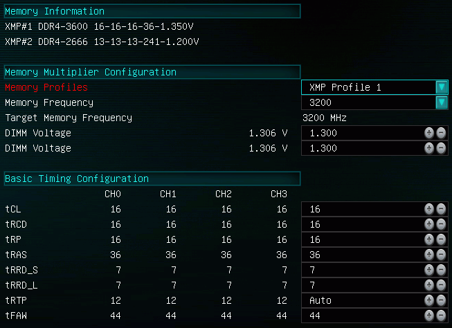
Image 59: Memory tuning page in X299 DARK BIOS setup.
Extreme OC tricks in BIOS
Some items in BIOS will cause the cold-boot power cycle, when the system automatically shuts down to apply the new parameters. It may be wise to apply this settings first for baseline profile and then modify voltages/ratios/memory settings for fine tuning without system power cycle. Settings that cause shutdown cycle include, but not limited to:
- BCLK adjustment, cause 2 power cycles to apply the setting
- CPU HyperThreading functionality – 1 power cycle
- CPU core count change – 1 power cycle
VCCIO, VCCPLL, VCCPLL_OC and VCCST voltages are crucial for LN2 overclocking to allow maximum performance out of Kaby Lake-X. These voltages need to be adjusted to higher levels to avoid cold-bug issues. Cold-bug is the condition when processor stop working or working unstable due to very low temperature. Kabylake-X with correctly set voltages can work and run benchmarks normally at minimum temperature of -196 °C (LN2 boiling temperature point).
Skylake-X CPUs are not as lucky for cold-bug issues, due to FIVR on the package. Normal operation temperature for extreme overclocking is -100 °C, with some CPUs going bit lower to around -110…-120 °C.
Watercooling compatibility
All X299 DARK boards shipped with standard LGA2011/LGA2066 ILM with threaded corner mounts backplate. Installing even large waterblock systems is no problem, thanks to increased spacing between DIMM slots and CPU socket. VRM Fans are recommended to use when using watercooling for CPU, especially if there is lack of chassis airflow. High-power CPUs, such as Core i9-7940X/7960X/7980XE pull over 400W even with very mild overclocking, so keeping VRM is essential for prolonged and reliable operation.
Few users requested waterblocks for the EVGA X299 DARK. EVGA at the moment of writing does not have own waterblock design, but we encourage after-market builders to design your own cooling solution. To help with this goal here are 3D CAD files with dimensions around VRM components.
EVGA X299 DARK R1.0 CAD-assembly file, ZIP-archive. Password : xdevs.com
EVGA X299 DARK R1.0 CAD-assembly dimensions drawing, PDF-file
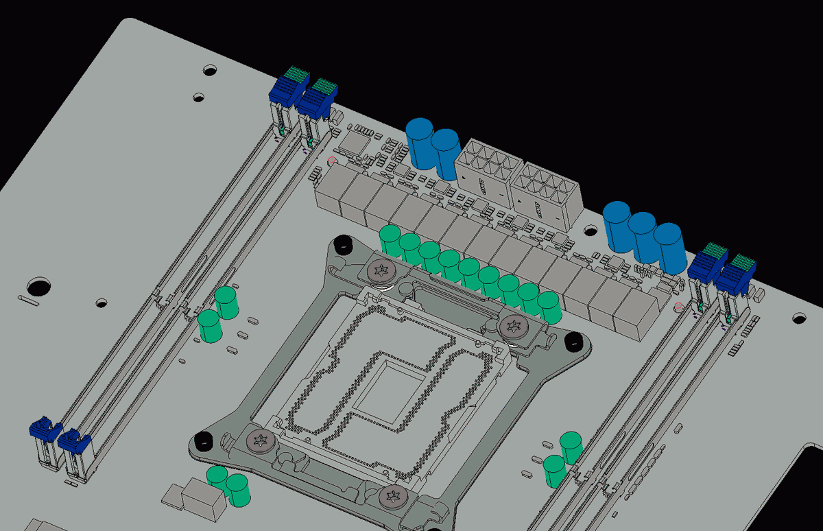
Image: CAD file view for EVGA X299 DARK with VRM component models.
Example waterblock shape for EVGA X299 DARK R1.0 VRM
Filter capacitors between the VRM power stages are TALLER (1.25 mm) than the MOSFET IC (0.66 mm) itself. So make sure that waterblock base have cutout slots on the base to clear those capacitors. Flat waterblock base may cause short of +12V input to ground and damage the components or board!
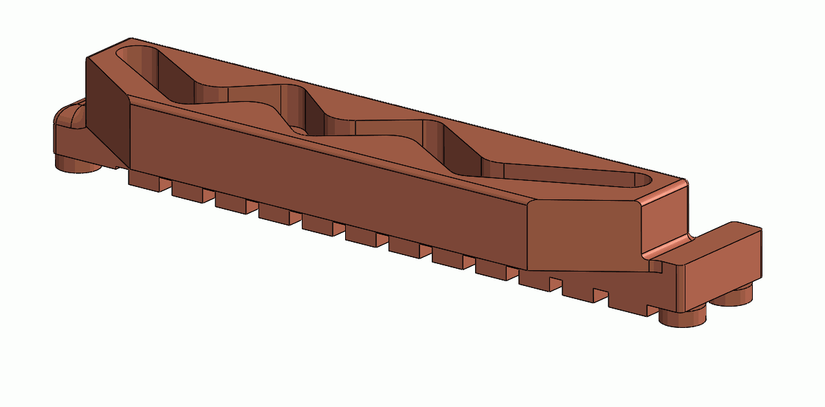
Image: Dummy waterblock shape example with base configuration for EVGA X299 DARK.
LN2 Extreme OC gear compatibility
X299 DARK is fully compatible with typical thru-hole mounting hardware that support LGA2011 socket hole 80 × 80 square spacing. Optional socket backplate without threaded mounts bundled with the every board package.
Additional spacing between the CPU socket and DIMM slots allow for larger containers and easier insulation.
Few words on CPU delidding
Processor IHS removal voids the Intel processor warranty, delidded CPUs are not accepted for RMA.
With X299 becoming first HEDT platform where Intel opted out using indium-soldered attachment for processor and copper heatspreader (IHS) lot of enthusiasts started heated comments on this topic. For matter of using processor on default stock conditions, stock thermal interface works well enough and fits all Intel specifications.
However, used PCM thermal interface between CPU heat-spreader and silicon die become a bottleneck with overclocking and elevated core voltages. We will not go into complex details why TIM was used instead of solid indium alloy to attach IHS with CPU. Metal thermal interfaces require addtional steps in manufacturing, since indium do not wet on nickel-plated copper IHS and silicon surfaces. To enable good contact surface treatment, such as gold plating is required.
Procedure, well known as “delidding” become widely popular by concerned enthusiasts in pursuit to improve the situation with load temperatures. Delidding the copper IHS to replace stock Intel TIM to high-performance grease, such as Kingpincooling.com KPx and then attaching IHS back can get noticeable thermal benefits. During our tests, maximum load temperature usually reduce 10-15 °C on Kabylake-X and 10-20 °C on larger Skylake-X processors.
Delidding is crucial for any serious extreme sub-zero overclocking, otherwise maximum stable frequency can be off as much as 400-600 MHz! Since extreme overclocking usually not covered by any kind of warranty, delidding procedure is the way to go if you interested in benchmarking for world records.
Now, time to get serious with overclocking all this technology to it’s limits. Be sure to read various online guides to get yourself familiar with terminology and idea. Good to have fresh clean OS install on the SSD drive, which does not have any important and precious data on it. Pretty often overclocking CPU and memory can generate random errors and Windows may corrupt the data on the drive and make it not bootable. OS imaging and backup software like Acronis or Paragon can save hours of OS and driver reinstalls in case of overclocking going sideways.
Skylake-X Refresh (i7-9800X and i9-99xxX models) and CascadeLake-X (109xx models) CPU have soldered metal thermal interface and different IHS design, so they do not require delidding for nearly all overclocking scenarios (including extreme LN2-cooled benchmarking).
Delidding soldered CPU require controlled heating and difficult to perform. Also the gain from replacing metal solder thermal interface to liquid paste in this case is much smaller, compared to CPUs with thermal paste interface IHS.
Overclocking methodology for Kaby Lake-X
Overclocking with Kaby Lake-X Core i5 and Core i7 processors is simple, same as regular desktop LGA115X models. CPU die itself is very same, so all overclocking features are working equally on X299 DARK, just like expected.
Air/water cooling clock/voltage/temperature range
With a good aircooling or watercooling setup that can handle full load temperatures under 80 °C common Skylake-X processors can reach stable frequency around 4.9-5.3 GHz on all four cores. Special loading cases using AVX-instructions drop this bar to about 4.6-4.8 GHz due to higher stress on processor. These numbers are valid only after processor delidding and replacement of stock TIM to high-performance grease, such as Kingpincooling.com KPx.
Good i7-7740X may be able to reach 5.4-5.5 GHz under watercooling solution, stable enough to run 3Dmark benchmarks and games:
Hot processors also draw more power and produce more heat, which increase stability risks compared to running processor cold. Constantly loaded system should not have temperatures above +80 °C, to ensure reliable long-term operation.
LN2 cooling clock/voltage/temperature range
| OC stage KabyLake-X | CPU frequency | Voltage levels |
|---|---|---|
| STEP 1, first 30-60 minutes | 1st boot/checks, CPU clock around 5 GHz | Around 1.4-1.5V |
| STEP 2, -40 to -60 °C | 5.5-5.7 GHz, DDR4 at 3.4-3.6GHz | 1.55 VCORE, 1.5VMEM |
| STEP 3, -90 to -110 °C | 5.8-6.2 GHz, DDR4 at 3.6-3.8GHz | 1.65 VCORE, 1.5VMEM |
| STEP 4, -120 to -140 °C | 6.2-6.4 GHz, DDR4 at 3.6-4.0GHz+ | 1.75 VCORE, 1.6VMEM |
| STEP 5, -160 °C and colder | 6.5-7.0 GHz, DDR4 at 3.6-4.0GHz+ | 1.85+ VCORE, 1.8V+MEM |
| STEP 6, Warmup back to ambient | 5.2-5.5 GHz, DDR4 at 3.4-3.6GHz | 1.55 VCORE, 1.5VMEM |
Table 9: Extreme overclocking steps and guidance
These are typical steps and LN2 scaling numbers of what most X299 DARK boards with decent CPU can achieve. While X299 DARK is indeed capable to push even the best CPU to it’s limits, the actual result still varies per specific CPUs silicon quality, stability of temperature control, used thermal grease properties and system/configuration + benchmark used. Factors such as chip leakage, container mounting pressure can and will have a impact on the end result.
Power requirements
Kabylake-X CPUs are very efficient and take under 200W of electrical power, even when slightly overclocked to near 5 GHz clocks.
Here all the testing will be done using Kabylake-X processor, 4-core i7-7740X.
| Component | Model Number |
|---|---|
| Motherboard | Production EVGA X299 DARK board, without heatsinks, BIOS Rev.1.0 |
| Processor | Intel Core i7-7740X Retail |
| DDR4 Memory | 2 × G.SKILL RipJaws V F4-3600C16D-GVK |
| Graphics card | EVGA GeForce GTX 1080 Ti KINGPIN Edition, aircooled |
| Power supply | EVGA SuperNova NEX 1500W 80Plus Gold, powered by Chroma 61504 2000 VA source |
| Cooling solution | EVGA CLC 240 Liquid cooler with additional high-power Delta fan |
| Storage | Intel 540s 120GB SATA SSD |
| Power measurement | Tektronix MDO4054C + TCPA300 amp + TCP303 150ADC + P6251 probe |
Table 10: Complete test system configuration for daily scenario
To allow accurate thermal imaging, heatsinks were REMOVED on any component of the board. Keep this in mind, since actual temperatures of board components in retail configuration, with all heatsinks and fans will be lower, than numbers reported here. Captured data is close to worst case scenario, equivalent with very low chassis airflow, with blocked heatsink locations.
System will be tested using various settings, in stock conditions and also overclocked, to evaluate how much additional stress is caused by operating processor, memory and graphic card outside of default specification.
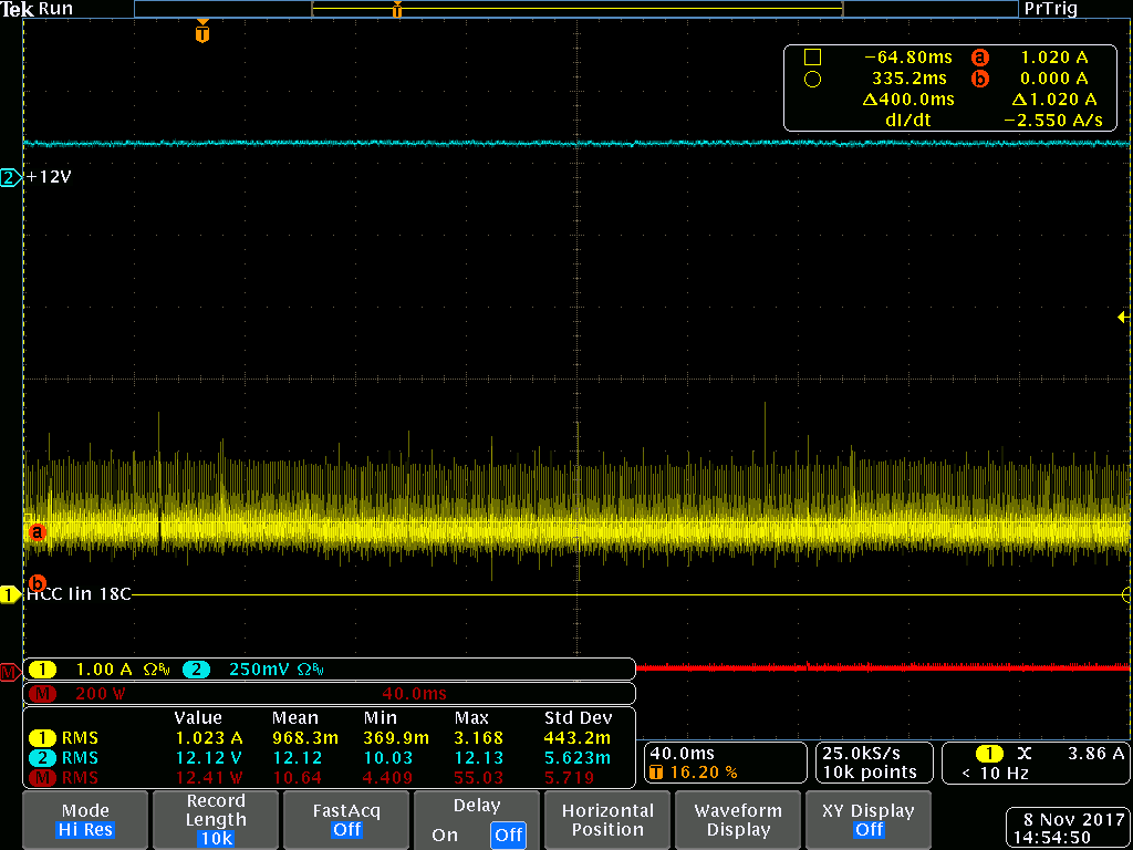
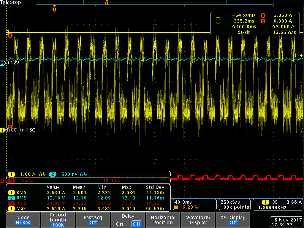
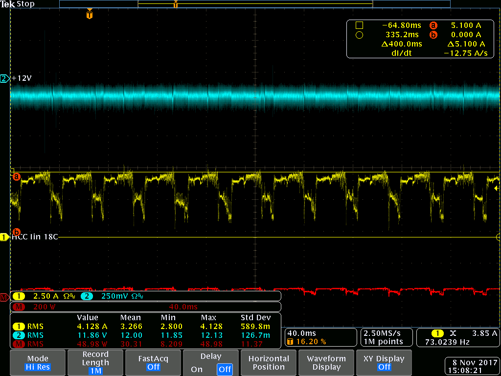
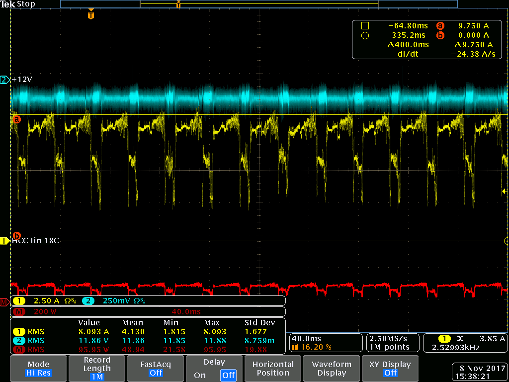
Here’s overview on the power measurement system. There are two points of measurement:
- AC Mains input to the system power supply to measure total power draw from the wall
- +12V CPU power input at both 8-pin CPU connectors from PSU to measure CPU power draw and VRM efficiency.
Also diagnostics software and onboard monitoring was used to read CPU VRM output power and current, so power loss at VRM could be calculated. All this data presented below, with condition details and temperatures captured in parallel.

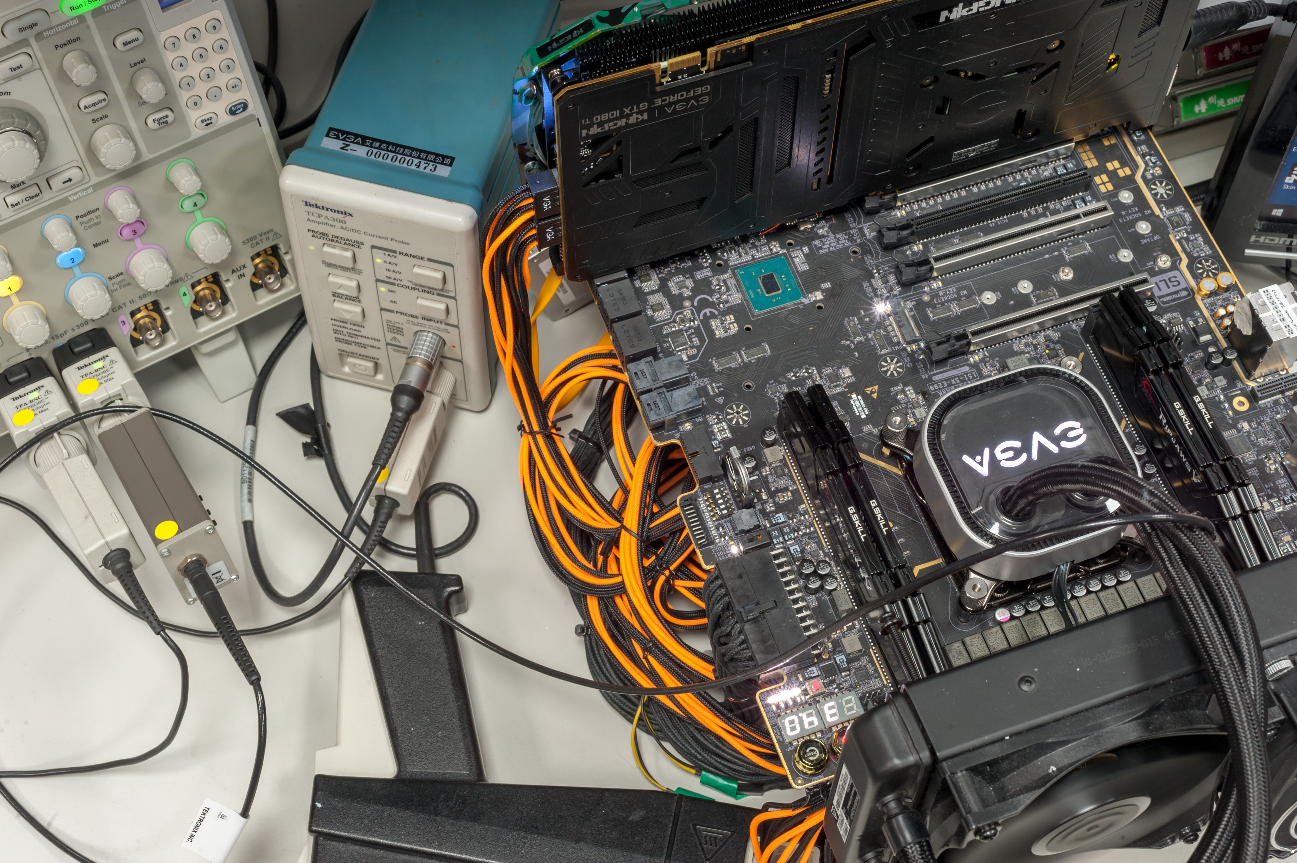
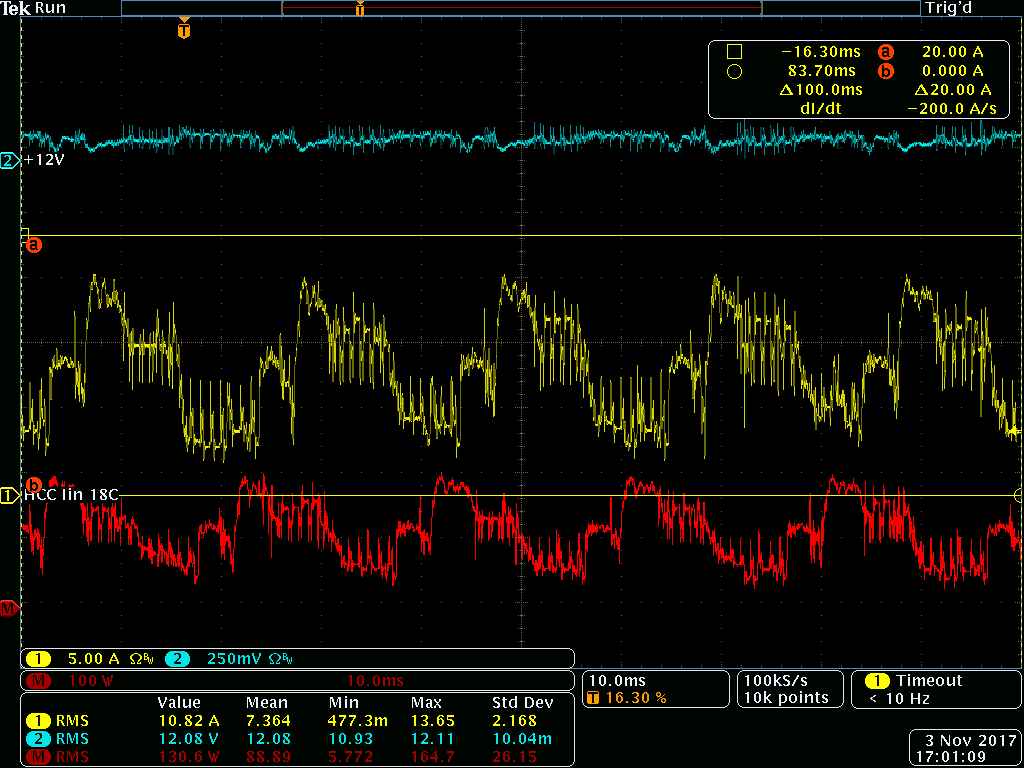
Image 60-61: Power measurement rig and probe connections.
Fluke Ti32 Infrared Camera helped in capturing hot-spots and detailed thermal images, thanks to it’s high resolution and SD card storage ability. Chroma 61504 AC Source used to generate mains 110VAC 60Hz sine voltage, provided to system ATX PSU. This 2000 VA source have integrated measurement circuit and to measure the steady and transient responses of true RMS voltage, current, true power, VA (apparent power), VAR (reactive power), power factor, current crest factor, peak repetitive current, and inrush current. This makes the 61504 not just an AC power source, but also an input power analyzer.
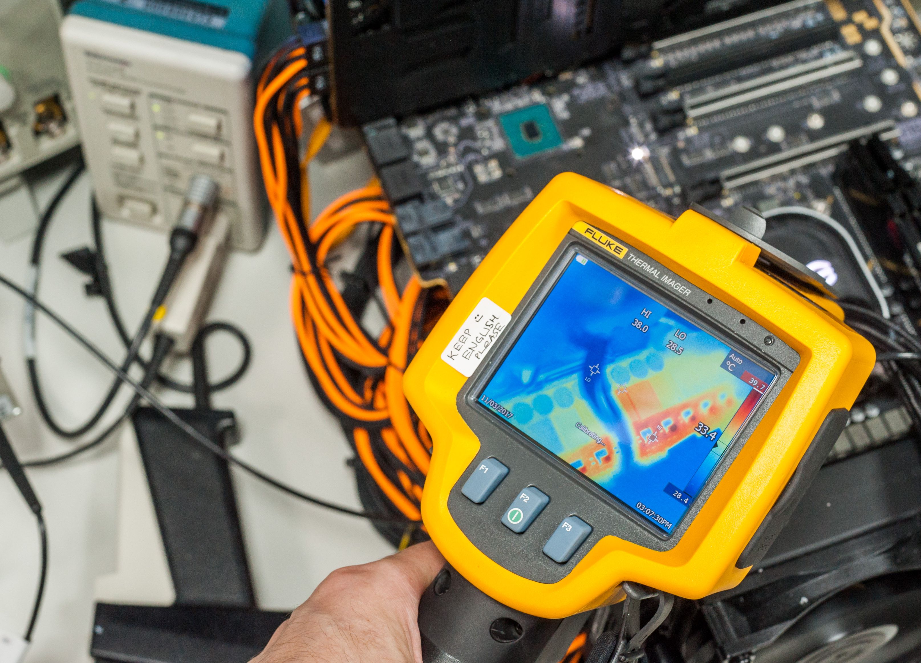

Image 62-63: Fluke Ti32 thermal imager and Chroma 61504 AC power source.
All this equipment will provide us decent accuracy and answer all power consumption questions, that many X299 system builders are eager to know.
Stock default conditions with Kabylake-X i7 CPU, no overclocking
First we get some baseline data, with default settings loaded in BIOS, and without any overclocking or voltage tuning.
| Condition | CPU VCCIN PRMS / PPEAK, W | PSU PINPUT, W | CPU Temperature, °C | VRM SPS Temp, °C | Thermal | Scope |
|---|---|---|---|---|---|---|
| BIOS idle GUI screen | 21 / 36 | 90 | +39 | +40 |  |
 |
| Windows Idle | 11 / 21 | 51 | +28 | +31 |  |
 |
| 3Dmark TimeSpy GT1 | 30 | 330 | +35 | +42 | 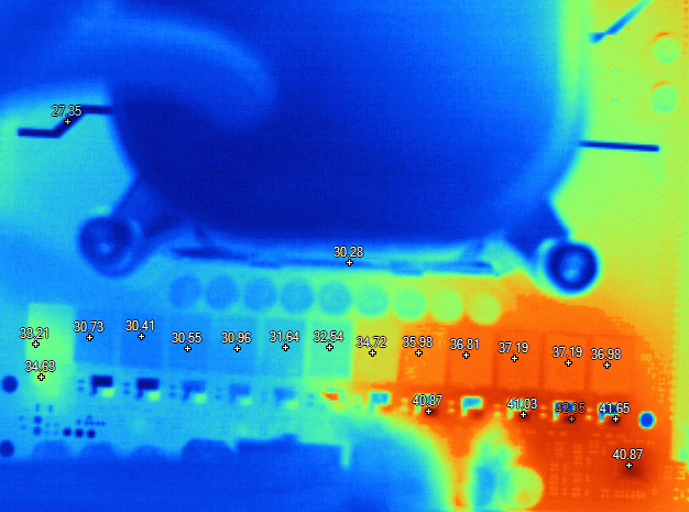 |
 |
| 3Dmark TimeSpy GT2 | 36 / 62 | 347 | +41 | +41 | 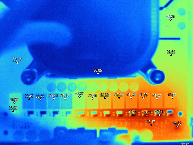 |
 |
| 3Dmark Physics test | 63 | 180 | +52 | +45 | 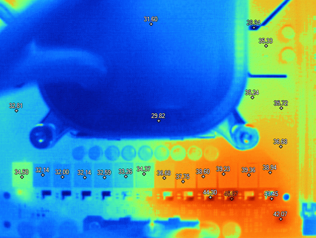 |
 |
| AVX constant load | 92 / 95 | 153 | +73 | +47 | 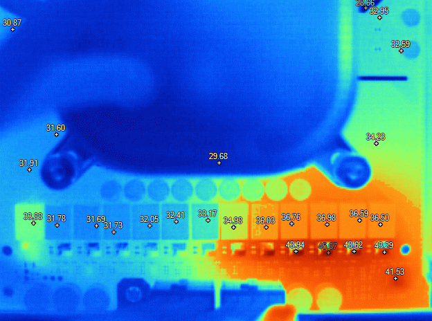 |
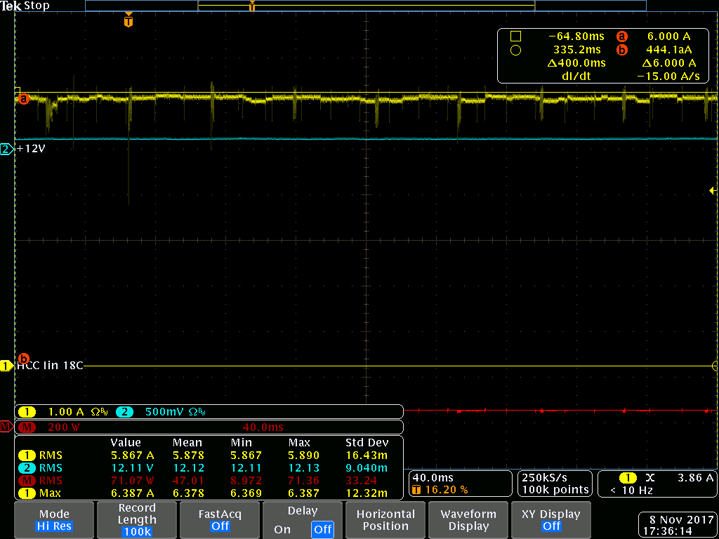 |
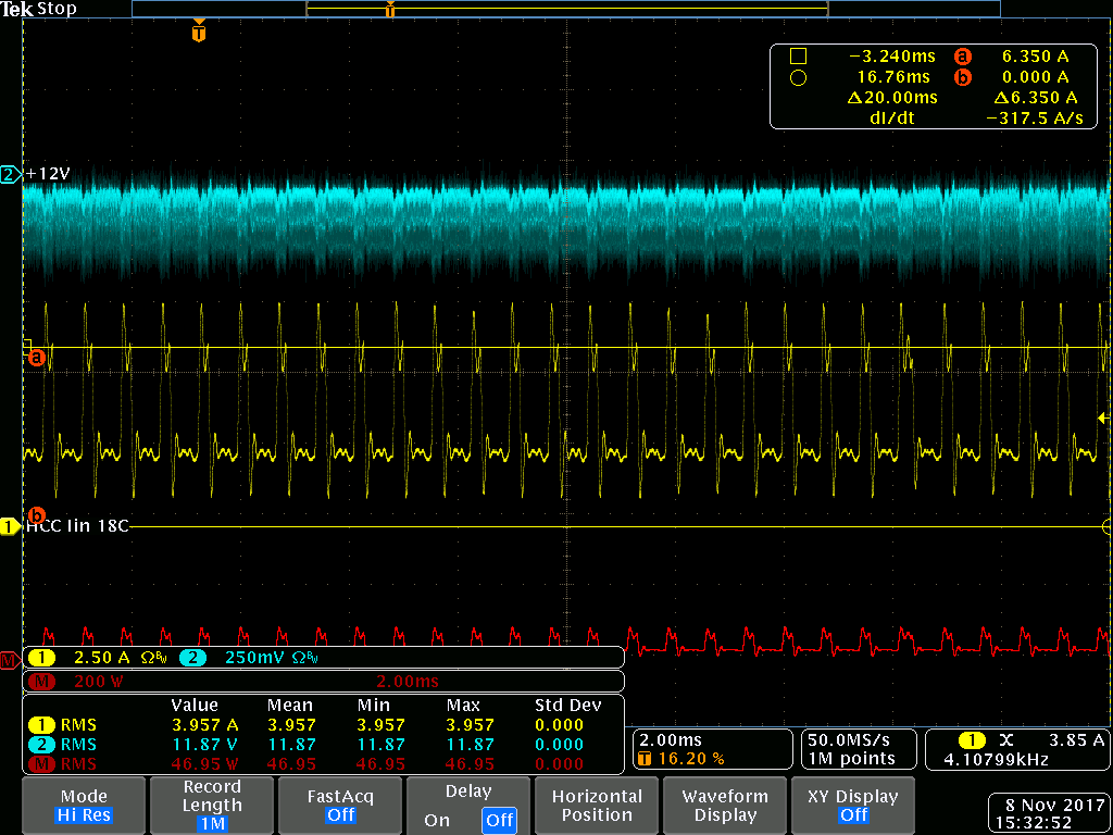
Table 11: Power and thermal measurements with stock i7-7740X.
As expected, X299 DARK VRM is heavily tuned for much demanding 18-core Skylake-X level processors and also for running Kabylake-X without any efforts required. Overclocking to 5 GHz is not going to change these numbers much, even with double of the power.
Overclocked system to 5.0 GHz Kabylake-X, 3.2GHz memory, elevated voltages.
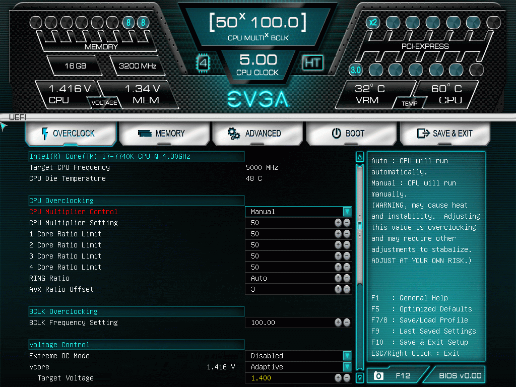

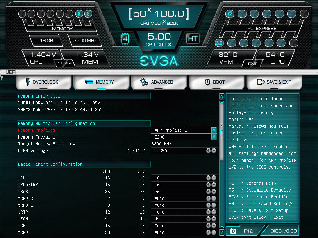
Image 64-65: OC settings for 5.0 GHz Core i7-7740X Kabylake-X.
| Condition | CPU VCCIN PRMS / PPEAK, W | PSU PINPUT, W | CPU Temperature, °C | VRM SPS Temp, °C | Thermal | Scope |
|---|---|---|---|---|---|---|
| BIOS idle GUI screen | 46 / 78 | 136 | +48 | +47 | 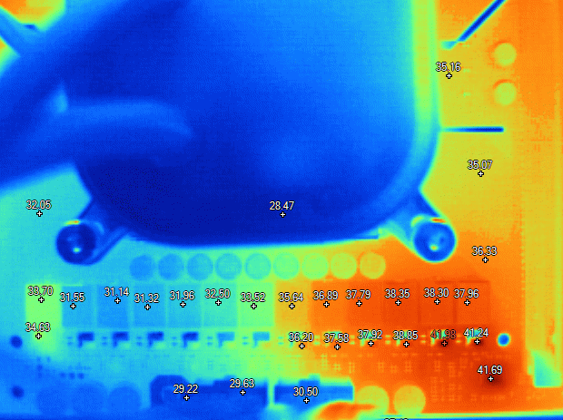 |
 |
| Windows Idle | 22 | 73 | +36 | +42 |  |
 |
| 3Dmark TimeSpy GT1 | 44 / 103 | 352 | +45 | +44 | 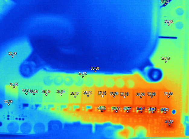 |
 |
| 3Dmark TimeSpy GT2 | 52 / 112 | 380 | +46 | +45 |  |
 |
| 3Dmark Physics test | 96 / 122 | 230 | +78 | +46 |  |
 |
| AVX constant load | 143 / 170 | 221 | +97 | +50 | 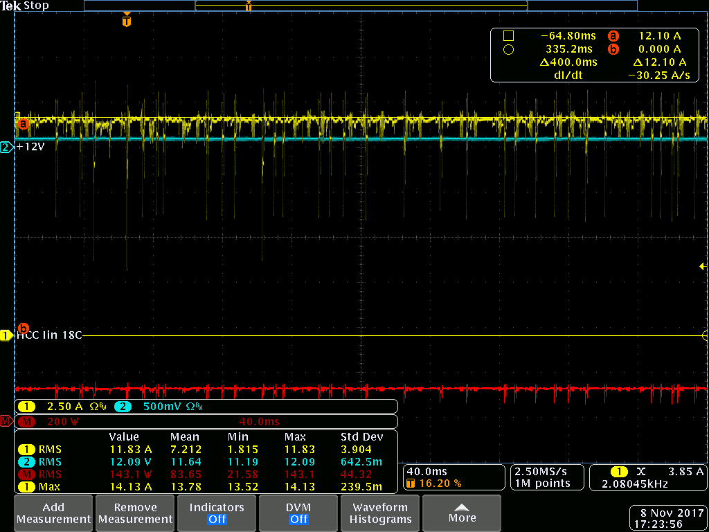 |
 |
Table 12: Power and thermal measurements with overclocked 5.0 GHz i7-7740X.
Overclocking methodology for Skylake-X
These CPUs have Turbo Boost Max Technology version 3.0, that allow to detect best 2 processor cores, whose maximum turbo frequency is few bins higher than the others. This can help for higher single-threaded load performance, when it’s assigned to run on such cores. Same technology was first introduced on Broadwell-E processors, where it allowed to see one best core. Best cores are different on each unique processor.
Intel has changed way the cores are interconnected internally from circular ring bus present in Haswell-E/Broadwell-E processors to mesh-type 2D-array interconnect. If you want to know more, new mesh topology is explained in Anandtech’s Skylake-X review. Nearly each Skylake-X processor can overclock safely with mesh frequency clock at 3200MHz (Mesh ratio 32 with 100.0 MHz BCLK). Pushing mesh further is increasingly troublesome and usually need higher mesh voltages and lower CPU temperatures. High mesh clocks can be quite helpful for 3D-intensive applications, such as 3Dmark or games.
Just like previous Haswell-E/Broadwell-E, Skylake-X CPUs use an FIVR, which is essentially an additional on-package power regulator. Motherboard supply higher (1.80 V default) voltage for the FIVR input, called VCCIN and then CPU power management controller and internal CPU package circuitry convert this voltage for low-level VCORE, VMESH and Uncore voltages. These voltages are not delivered by the motherboard directly as a result.
FIVR is also one of the key reasons why temperature range for extreme overclocking on Skylake-X CPUs is capped around -100 °C. Inductance, impedance and power delivery quality highly affected by temperature, and if these internal processor components get too cold – FIVR protection mechanisms will kick in, resulting in system power down or internal voltage rail shutdown. Same design limitation exists in previous FIVR-based processors, such as Haswell-E and Broadwell-E on old X99 platform.
Other voltages, such as VCCIO and DIMM voltage are still generated on the motherboard by common regulators.
Another way to increase platform performance is to adjust BCLK frequency. BCLK overclocking, unlike ratio overclocking increasing all the internal processor frequency blocks simultaneously, as most of them are derived from the input BCLK. To prevent issues with PCIe operation, this domain (and the DMI link to PCH) use fixed separate clock at 100 MHz, coming from the external BCLK controller. Memory controller and DDR4 clock multipliers are also derived from system BCLK, so it all adjusted in sync.
BCLK with Skylake-X can be changed in fine increments ~±5% from the default 100 MHz frequency, with help of BIOS control and external clock generator chip. Additional “gear” ratios are also available, allowing to jump 100 MHz base frequency to 125 MHz or 167 MHz. This allow bit more flexibility for DDR4 overclocking, still leaving PCIe/DMI to operate at nominal 100 MHz.
| BCLK ratio = 1:1 | BCLK ratio = 5:4 | BCLK ratio = 5:3 | |
|---|---|---|---|
| CPU BCLK minimum | at least 93 MHz | at least 117 MHz | at least 154 MHz |
| CPU BCLK nominal | 100 MHz | 125 MHz | 167 MHz |
| CPU BCLK maximum | at least 107 MHz | at least 133 MHz | at least 177 MHz |
| PCIe/DMI clock | 100 MHz | 100 MHz | 100 MHz |
| DDR4 clock | 2666 MHz : BCLK ratio = 2666 MHz | 2666 MHz : BCLK ratio = 3333 MHz | 2666 MHz : BCLK ratio = 4443 MHz |
Table 13: BCLK overclocking ranges and ranges.
BCLK ratio on X299 DARK is handled automatically by BIOS, so you can just enter desired frequency and ratio will be set automatically. For example if user enter 127 MHz, then 125 MHz ratio will be activated and +1.6% internal clock increase will be programmed, resulting in final BCLK frequency 127.00 MHz.
BCLK ratios can be changed only from the BIOS GUI, as it require additional cold-boot power cycle to properly programm all internal CPU registers. System will perform two automatic power cycles once new BCLK setting is applied.
Pushing 167 MHz may be difficult on some CPU samples, as it’s the most stressful configuration for the processor and memory controller to operate. High BCLK clocks may require increase of VSA, VCCIO and VIN voltages for stability. Also don’t forget to adjust CPU, MESH and DDR4 ratios accordingly, so final frequency on these components does not go out of the range with high BCLK.
Air/water cooling clock/voltage/temperature range
With good aircooling or watercooling setup that can handle full load temperatures under 70 °C common Skylake-X processors can reach stable frequency around 4.5-4.7 GHz on all cores. Special loading cases using AVX-instructions drop this bar to about 4.1-4.2 GHz due to much higher stress and power requirements.
Good starting point for the ambient cooling system listed in table below.
| Parameter | i7-7800X and 7820X | i9-7900X, i9-7920X | i9-7940X and above |
|---|---|---|---|
| CPU Temperature | lower than +70 °C under full loading | ||
| CPU Turbo Clock | 4700 MHz | 4600 MHz | 4500 MHz |
| CPU Voltage | Adaptive, 1.3V | Adaptive, 1.275 V | Adaptive, 1.25 V |
| MESH Clock | 3200 MHz | ||
| MESH Voltage | Adaptive, 1.2 V | ||
| CPU VIN Voltage | 2.0 V | 1.9 V | |
| VCCIO Voltage | 1.1 V | 1.25 V | |
| Uncore Voltage | +250 mV | ||
| DIMM Voltage | 1.5 V | ||
| DIMM settings | 3600 MHz 14-14-14 or better | ||
Table 14: Typical starting points for ambient cooling overclocking.
Make sure that performance is correct (true for any settings, change, not just these listed in table) and there is no throttling happening. Sometimes it is easy to get carried away by high clocks, only to discover later that its only decreased actual system speed in benchmarks. VCCIN voltage level is particulary sensitive for CPU power management operation.
High-core count processors such as i9-7960X or i9-7980XE may drop few hundred MHz from maximum stable clock, mostly due to the thermal limitations.
Hot processor also draws more power and produces more heat, which increases stability risks, compared to running processor cold. Long, constant loaded system should have temperatures above +80 °C, to ensure reliable long-term operation.
LN2 cooling clock/voltage/temperature range
LN2-cooled rig with temperatures about -80..-90 °C Skylake-X processors can reach very high clocks, at least around 5.6-5.7 GHz, on all cores. Special loading cases using AVX-instructions drop this bar to about 5.4-5.5 GHz due to much higher stress and power requirements. These numbers are valid only after processor delidding and replacement of stock TIM to high-performance grease, such as Kingpincooling.com KPx.
Table 15 provide a starting point for the extreme cooling with CPU temperature in -90 °C…-110 °C range.
| Parameter | i7-7800X and 7820X | i9-7900X, i9-7920X | i9-7940X and above |
|---|---|---|---|
| CPU Temperature | below -80 °C but above coldbug threshold | ||
| CPU Turbo Clock | 4700 MHz | 4600 MHz | 4500 MHz |
| CPU Voltage | Adaptive, 1.3V | Adaptive, 1.275 V | Adaptive, 1.25 V |
| MESH Clock | 3200 MHz | ||
| MESH Voltage | Adaptive, 1.2 V | ||
| CPU VIN Voltage | 2.0 V | 1.9 V | |
| VCCIO Voltage | 1.1 V | 1.25 V | |
| Uncore Voltage | +250 mV | ||
| DIMM Voltage | 1.5 V | ||
| DIMM settings | 3600 MHz 14-14-14 or better | ||
Table 15: Typical starting points for extreme overclocking LN2 cooling overclocking.
High-core count processors such as i9-7960X or i9-7980XE may drop few hundred MHz from maximum stable clock, mostly due to the thermal limitations. Decent i9-7980XE CPU sample, cooled to -100 °C well able to complete 3D benchmarks like 3Dmark Time Spy or Fire Strike running at 5.7 GHz, all cores enabled.
Power requirements
Same test setup and equipment was used to measure power consumption and thermal performance of Skylake-X system as well.
| Component | Model Number |
|---|---|
| Motherboard | Production EVGA X299 DARK board, without heatsinks, BIOS Rev.1.0 |
| Processor | Intel Core i9-7980XE 18-core processor |
| DDR4 Memory | 4 × G.SKILL RipJaws V F4-3600C16D-GVK |
| Graphics card | EVGA GeForce GTX 1080 Ti KINGPIN Edition, aircooled |
| Power supply | EVGA SuperNova NEX 1500W 80Plus Gold, powered by Chroma 61504 2000 VA source |
| Cooling solution | EVGA CLC 240 Liquid cooler with additional high-power Delta fan |
| Storage | Intel 540s 120GB SATA SSD |
| Power measurement | Tektronix MDO4054C + TCPA300 amp + TCP303 150ADC + P6251 probe |
Table 16: Complete test system configuration for daily scenario, Skylake-X version
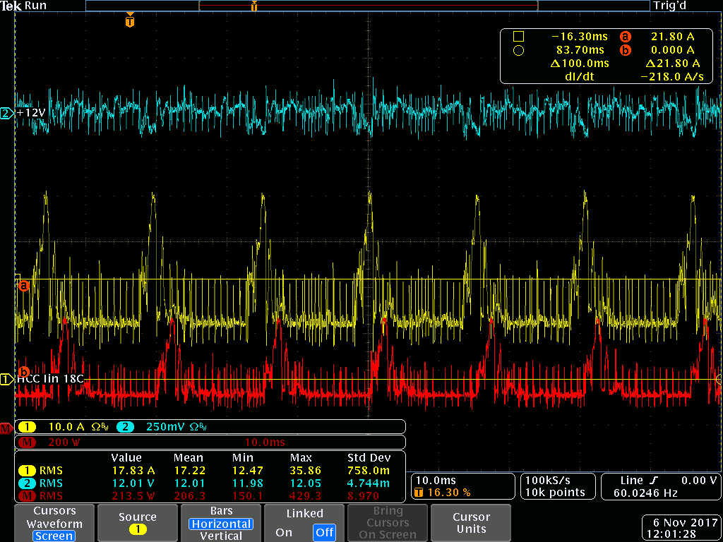
Stock default conditions with i9-7980X Skylake-X, no overclocking
First we get some baseline data, with default settings loaded in BIOS, and without any overclocking or voltage tuning.
| Condition | CPU PRMS / PPEAK, W | CPU VCCIN PPEAK, W | PSU PINPUT, W | CPU Temperature, °C | VRM SPS Temp, °C | Thermal | Scope |
|---|---|---|---|---|---|---|---|
| BIOS idle GUI screen | 53 | 125 | +35 | +41 | |||
| Windows Idle | 21 | 75 | +33 | +38 |  |
 |
|
| 3Dmark TimeSpy GT1 | 71 | 377 | +36 | +40 | 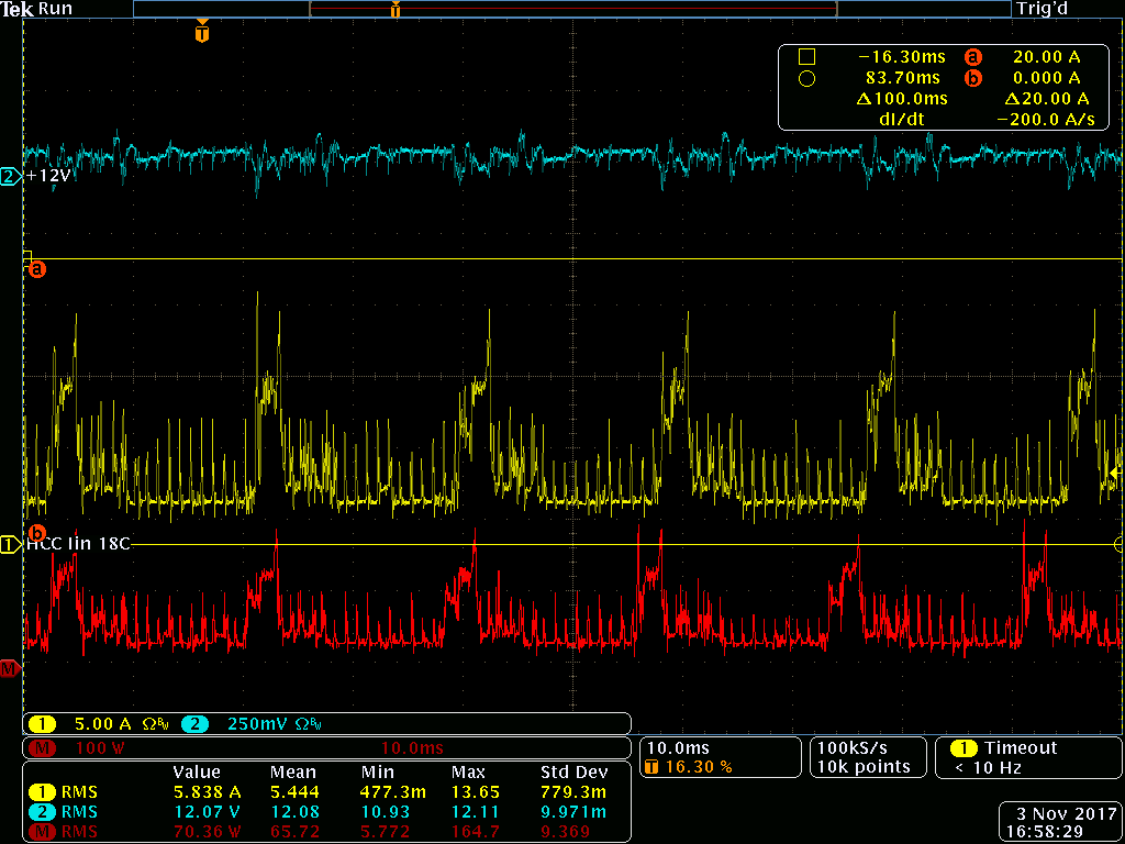 |
||
| 3Dmark TimeSpy GT2 | 76 | 385 | +37 | +44 | 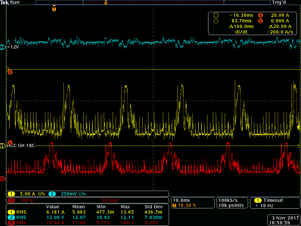 |
||
| 3Dmark Physics test | 130 | 235 | +40 | +47 | 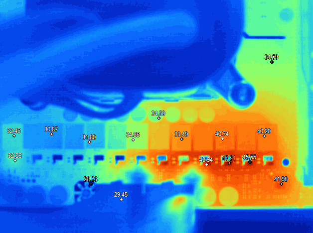 |
 |
|
| AVX constant load | 165 | 197 | 312 | +44 | +56 | 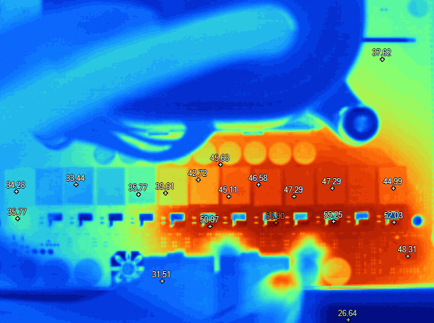 |
 |
| XTU CPU Stress | 142 | 192 | 288 | +42 | +54 | 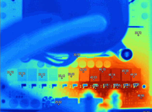 |
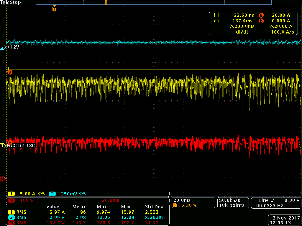 |
Table 17: Skylake-X stock thermal and power measurements.
Few additional thermal images for overall system:
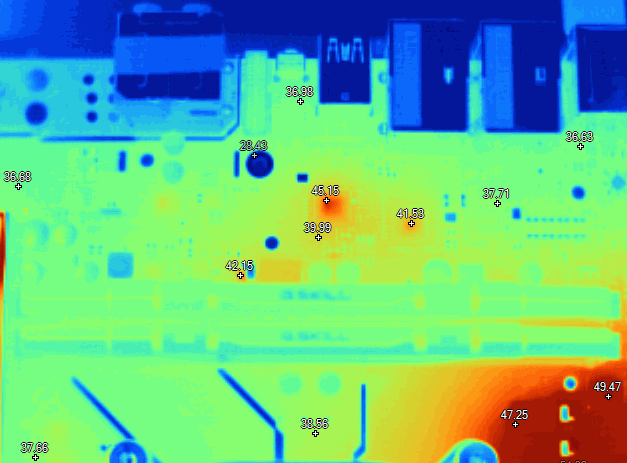
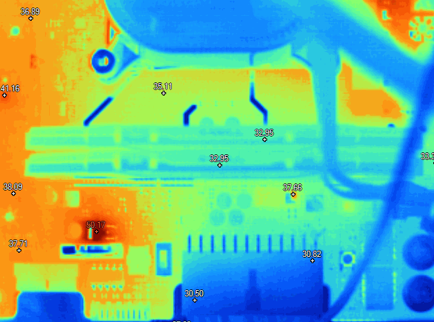
Image 66-67: Thermal images of memory sections and memory VRMs
Naked PCH and graphics card during the test:
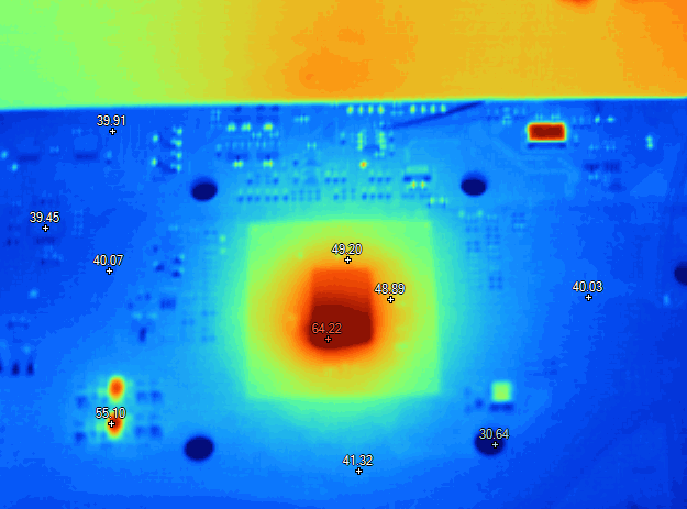
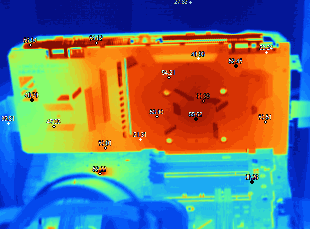
Image 68-69: Thermal images of PCH area and EVGA GeForce GTX 1080 Ti KP in PE4 PCIe slot.
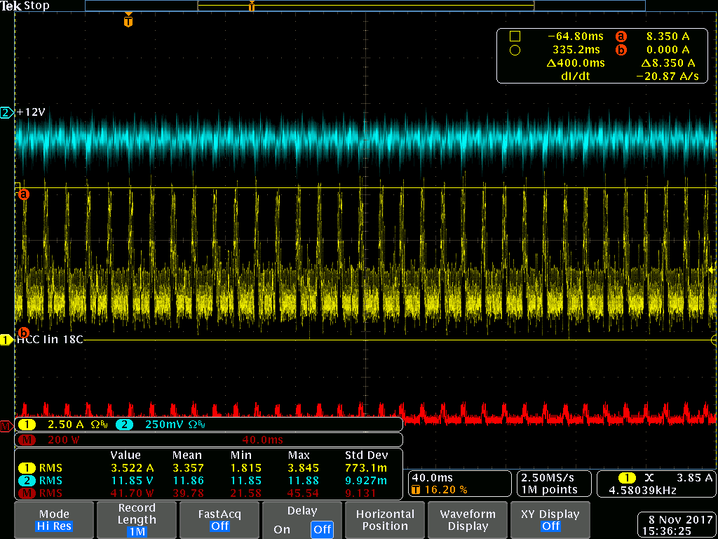
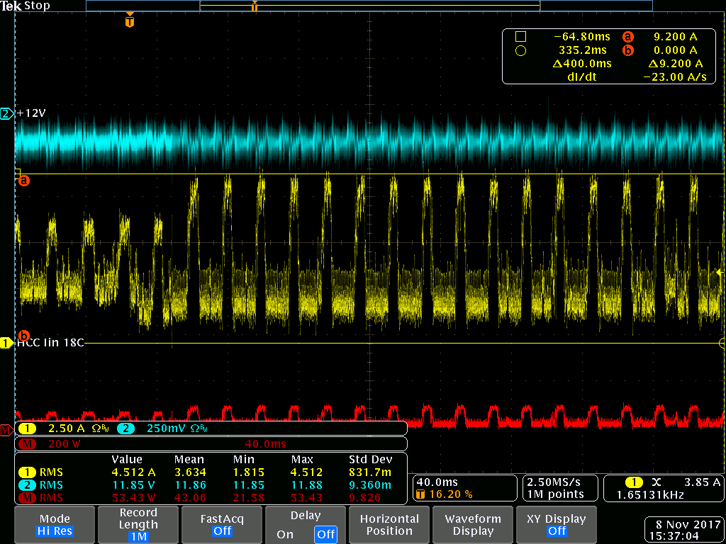
Overclocked system to 4.7 GHz i9-7980X, 3.2GHz memory, elevated voltages.
Overclocking processor to 4.7 GHz was straightforward, just setting CPU ratio to 47, bumping MESH ratio to 30, adjusting voltages a little and settings XMP memory profile to Profile 1, and reducing memory frequency to 3200 MHz.
High-speed fan on watercooling radiator was used to ensure decent temperatures under stress loading. Power measurement data presented below:
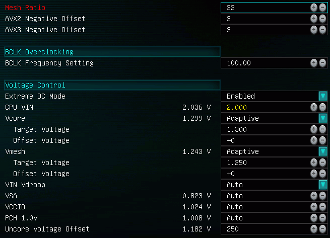
Image 70: OC settings for 4.7 GHz Core i9-7980XE Skylake-X.
| Condition | CPU PRMS / PPEAK, W | CPU VCCIN PPEAK, W | PSU PINPUT, W | CPU Temperature, °C | VRM SPS Temp, °C | Thermal | Scope |
|---|---|---|---|---|---|---|---|
| BIOS idle GUI screen | 227 | +46 | +45 | ||||
| Windows Idle | 152 | 215 | +38 | +41 | 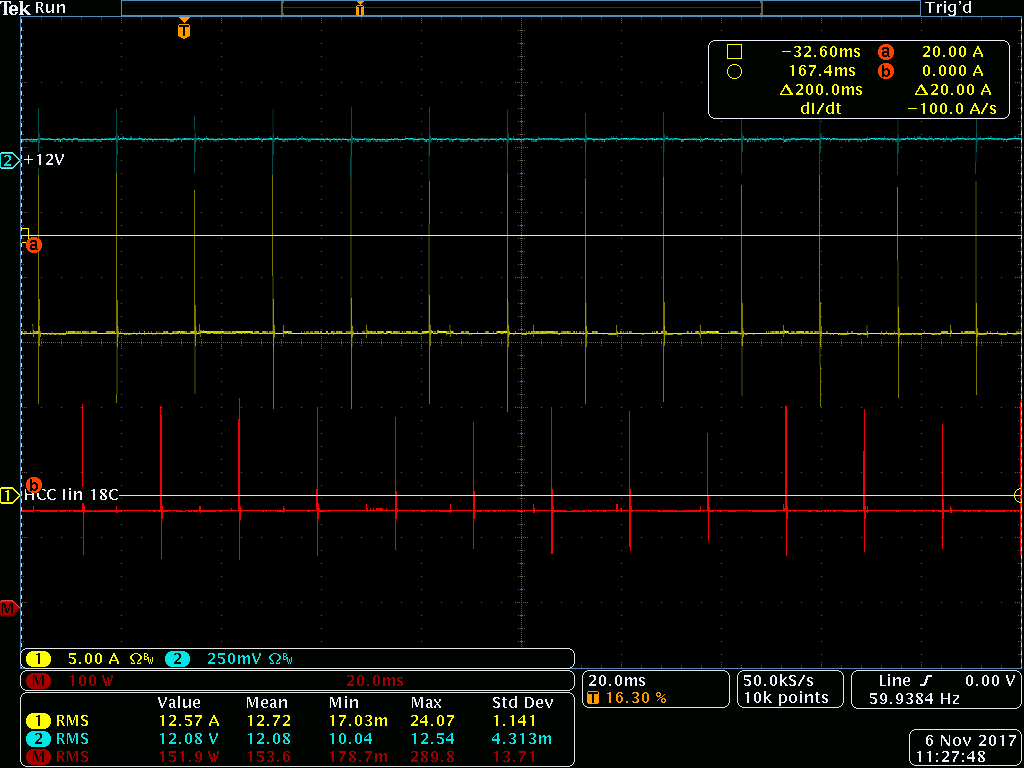 |
||
| 3Dmark TimeSpy GT1 | 191 | 544 | +46 | +47 | 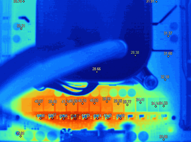 |
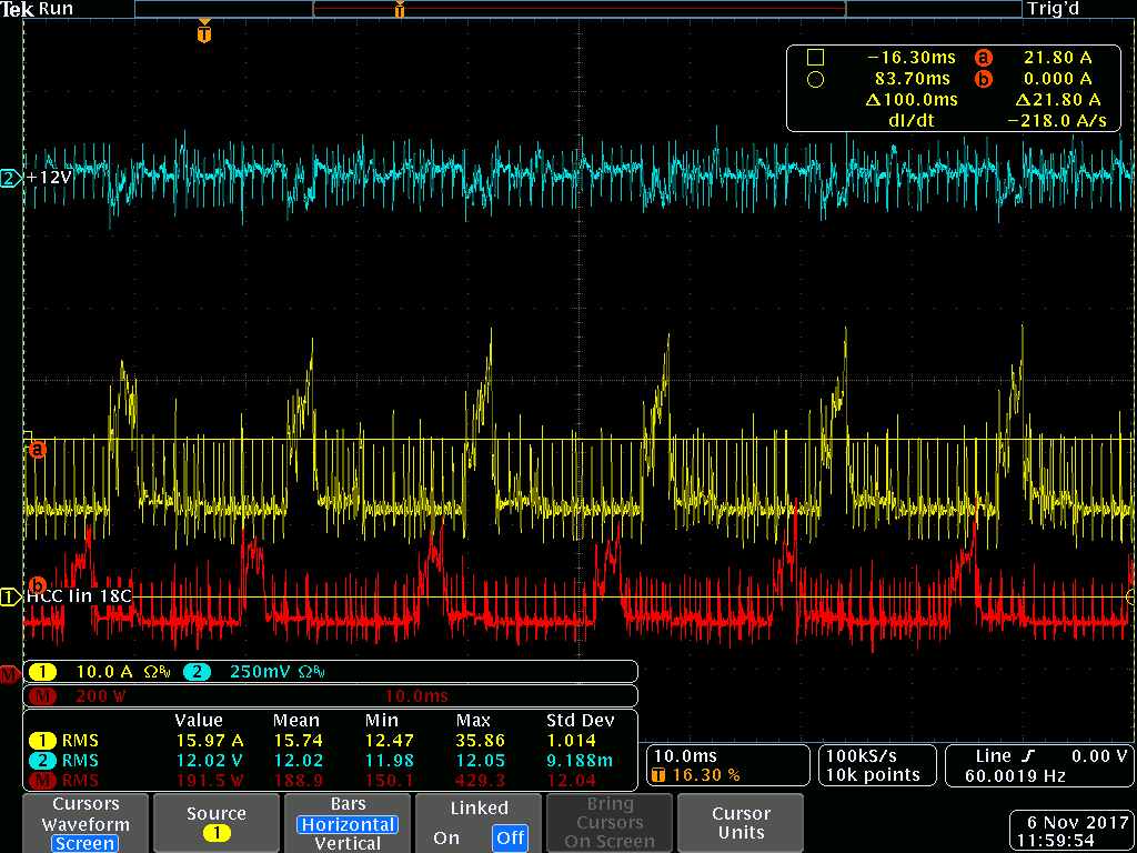 |
|
| 3Dmark TimeSpy GT2 | 213 | 585 | +48 | +46 | 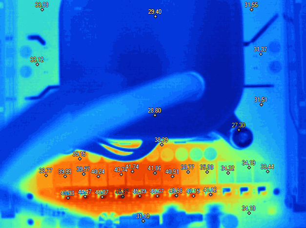 |
 |
|
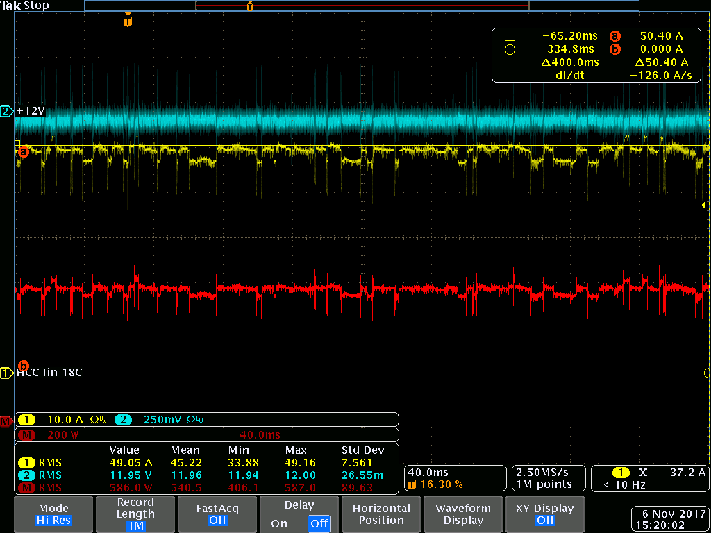
| 3Dmark Physics test | 358 | 510 | +56 | +63 |  |
 |
|
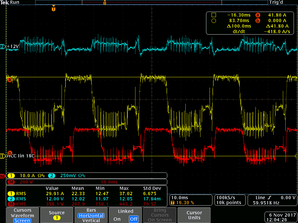
| AVX constant load | 586 | 740 | +94 | +78 | 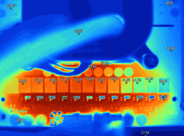 |
 |
|
| XTU CPU Stress | 406 | 560 | +63 | +75 | 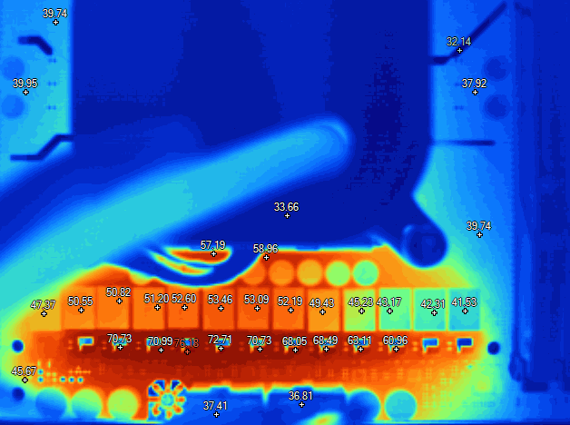 |
 |
Table 18: Skylake-X stock thermal and power measurements.
As conclusion, you are much more likely to hit thermal limits of processor itself during the overclocking than VRM thermal headroom limitations, no matter what CPU is used.
DDR4 Memory overclocking (both CPU types)
For better understanding how system memory is working let’s dig into small theory topic. RAM cells do not store any data when powered off, as each bit in memory represented by tiny charge storage block. You can imagine tiny capacitor as such block, which can store charge if bit is high “1” or does not have charge for zero “0” state. Once power is removed, charge will dissipate and data will be lost forever.
Before DDR4 system memory can function propertly, it must “train”. The term “training” in the context of memory operation applies to adjustment and tuning procedures that are performed by the memory controller inside CPU and BIOS. Due to wide bus and big distance between CPU silicon and DDR4 chip training is required to adjust and measure signal propagation delays, specific to each instance of motherboard, connectors and memory module. Every piece of hardware is little different, and training allows determination of the delay adjustments to guarantee that bits like zeros and ones arrive at proper timing between the devices.
Based on test results, using various Kabylake-X and Skylake-X CPUs on multiple boards, optimal DDR4 clock range is in 3400-3600 MHz for everyday use.
X299 DARK has large set of available memory ratios to fit any DDR4 memory module frequency requirements.
| Memory feature | Kabylake-X CPU | Skylake-X CPU |
|---|---|---|
| Minimum DDR4 ratio | 1000 MHz (10 * BCLK) | |
| Default DDR4 ratio | 2666 MHz | 2400 MHz for i7-7800X, 2666 MHz for rest |
| Maximum DDR4 ratio | 4133 MHz | 4133 MHz |
Table 19: Memory overclocking ranges.
Memory overclocking with Skylake-X is similar to the Kabylake-X, with difference around one or two ratios down. Same memory modules are able to achieve similar frequency, even when used in quad-channel configuration. All four DDR4 DIMM slots are equally matched in terms of memory clocks, so there is no recommended slot for maximum memory frequency clocks.
For practical overclocking and benchmarking going for maximum memory frequency is rarely the best, as higher than 3600 MHz frequencies require loosening timings and increase of the DDR4/Uncore voltages. Using high-speed XMP-rated DIMM sticks however is helpful, since high-end memory binned for better memory IC. As result good XMP-4133 modules can deliver best performance running at some optimized settings, such as 3600 MHz with tight timings 13-13-13-1T using just moderate voltage bump to 1.4-1.55 VDIMM.
Summary
Happy benching and gaming! If you have any comments or question, join us in comment section at the right side of this article or discuss at KPC Forum.
Here are some record results, obtained using EVGA X299 DARK and EVGA GeForce GTX 1080 Ti Kingpin Edition graphics card(s).
- 19591 3Dmark, Time Spy Extreme, i9-7980XE @ 5624 MHz with 4-way SLI.
- 37596 3Dmark, Time Spy, i9-7980XE @ 5720 MHz with 4-way SLI @ 2455 MHz.
- 14507 3Dmark, Time Spy, i9-7980XE @ 5600 MHz with single card @ 2607 MHz.
- 31946 3Dmark, Fire Strike Ultra, i9-7980XE @ 5720 MHz with 4-way SLI @ 2404 MHz.
- 49352 3Dmark, Fire Strike Extreme, i9-7980XE @ 5720 MHz with 4-way SLI @ 2404 MHz.
- 19616 3Dmark, Fire Strike Extreme, i9-7960X @ 5500 MHz with single card @ 2607 MHz.
- 58024 3Dmark, Fire Strike, i9-7980XE @ 5720 MHz with 4-way SLI @ 2354 MHz.
- 36421 3Dmark, Fire Strike, i9-7980XE @ 5720 MHz with single card @ 2607 MHz.
- 29165 3Dmark, Fire Strike Physics test, i9-7980XE @#64; 5750 MHz.
- 72456 3Dmark Cloud Gate, i9-7980XE @ 5800 MHz with single card @ 2303 MHz.
- 45956 3Dmark 11 Performance, i9-7980XE @ 5750 MHz with single card @ 2581 MHz.
- 118631 3Dmark Vantage, Performance, i9-7980XE @ 5600 MHz with single card @ 2607 MHz.
- 6105.7 MHz CPU-Z validation, i9-7960X, -108 °C LN2 cooled.

Feel free to share and link to this guide, but keep links and all references intact, as this guide will be updated in future.
© Vince “K|NGP|N” Lucido & Illya “TiN” Tsemenko
Projects like this are born from passion and a desire to share how things work. Education is the foundation of a healthy society - especially important in today's volatile world. xDevs began as a personal project notepad in Kherson, Ukraine back in 2008 and has grown with support of passionate readers just like you. There are no (and never will be) any ads, sponsors or shareholders behind xDevs.com, just a commitment to inspire and help learning. If you are in a position to help others like us, please consider supporting xDevs.com’s home-country Ukraine in its defense of freedom to speak, freedom to live in peace and freedom to choose their way. You can use official site to support Ukraine – United24 or Help99. Every cent counts.
Modified: Jan. 2, 2023, 8:28 a.m.