Contents
- Intro
- Warnings & Disclaimers
- RTX 2080 Ti KPE design goals and target audience
- EVGA KINGPIN Edition Series features
- What is all this VirtualLink thing?
- GDDR6 memory and its overclocking
- Power target and OC settings
- Few notes on GPU quality
- VRM design overview, available tuning and hardware controls
- Integrated OLED functionality
- Real voltage software monitoring
- BIOS & Tools
- EVGA Precision X1 software
- Watercooling compatibility
- Temperatures impact on GPU overclocking headroom
- LN2 Extreme OC cooling compatibility
- Summary
Intro
This is no usual review of a graphics card, it is yet another technical guide focused on design details and various OC features. EVGA RTX 2080Ti Kingpin Edition graphics card is based around new ray trace-enabled NVIDIA Turing TU102 ASIC and Samsung GDDR6 DRAM. Almost 2 decades ago I was playing with 3D Studio MAX and rudimentary raytracing Mental Ray engine that was available back then. Remember talking whole night to render single 1600×1200 scene with enabled raytracing on powerful (for the year 2000) AMD K7 system. Now we have a GPU card that can render the real-time flow of raytraced scenes in 4K resolution and do a whole lot more.
But this article is all about hardware, so before diving into it, might be worthy to refresh memory with the previous series of our hardware OC guides:
- EVGA GTX 1080 Ti K|NGP|N Edition graphics card
- Reference GTX 1080 Ti – Uncorking bigger Pascal
- Reference GTX 1080/1070 – Uncorking Pascal
- EVGA GTX 980 Ti K|NGP|N OC Guide
- Using Raspberry Pi to control EPOWER VRM
RTX 2080 Ti KPE design goals and target audience
RTX KPE designed to be greatest and mightiest all-around high-end GFX adapter, and its usage extends far beyond LN2-only benchmarking. Everyday gaming and graphics intensive workload readiness was one of the key goals to meet in development and fine-tuning stages. High power and strict temperature demands of Turing TU102 silicon required effective water-cooling design.
NV’s TurboBoost functionality is also very sensitive to GPU die temperature and stable boost clocks required keeping temperatures under +60 °C loaded, at all times possible. That left no headroom for air-cooled 2080 Ti KPE version, and only options available now are Hybrid with dual rad or HydroCopper with full-cover custom loop waterblock.
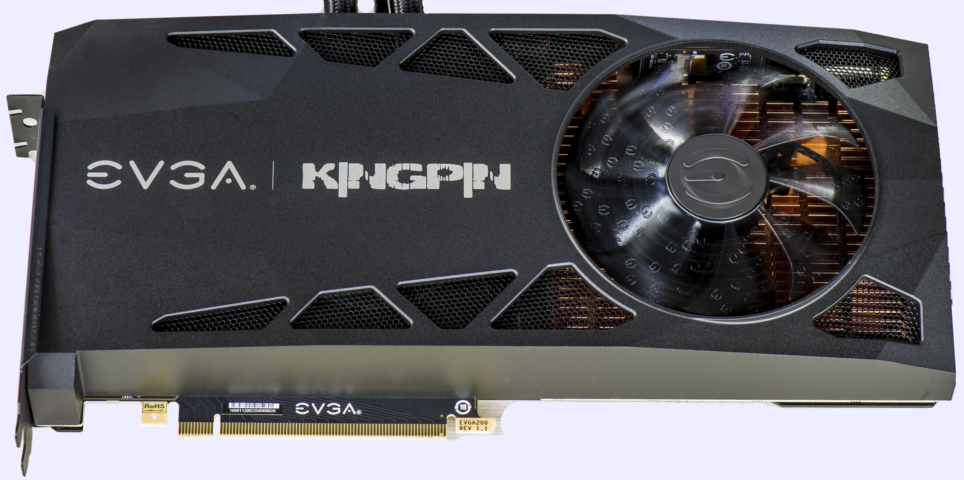
Image 1: EVGA RTX 2080 Ti KPE graphics card (radiator not shown)
Traditionally, Kingpin-tier cards have provisions for extreme overclocking, but those are not limiting or making the card any worse as a daily driver. If you looking for a very fast card with flexible OC headroom potential, KPE is suited for that best with onboard advanced monitoring functionality, high-power VRM design, and optimized BIOS. There are also many knobs available to fine-tune the card for your specific needs, which aren’t present or usually hidden on typical RTX 2080 Ti graphics card.
Warnings & Disclaimers
Consider everything given below as “educational material” and provided AS IS to aid in the understanding of the true power in your shiny new KINGPIN-branded card. Proceed with caution and at your own risk as only you are responsible for the possible outcome of out of spec stress.
Overclocking/overvoltaging your EVGA RTX 2080 Ti KINGPIN graphics card disregarding type of the cooling, is quite an adventure and usually safe for the hardware, as long as it’s done correctly. Always pay attention to details and fully research these topics before doing any VGA alterations. This guide will help with some key information and specifics.
Having patience and doing things in small incremental steps is key. Testing after each and every modification will provide the best user experience while keeping your hardware safe and benching over and over again. Data provided in this guide was verified on multiple cards to best effort, but slight variations in numbers or results for graphics adapters are still possible due to different test conditions and running environment.
EVGA does allow the end-user to perform a standard replacement of the cooling solution on the graphics card without losing the product warranty, but that only applies if the device was not mechanically or electrically altered. RMA inspection along with circuitry on the card can reveal modifications, even reverted. Always be honest and responsible for your actions with this enthusiast product.
Redistribution and use of this article, any parts of it or any images or files referenced in it, in source and binary forms, with or without modification, are permitted provided that the following conditions are met:
- Redistributions of the article must retain the above copyright notice, this list of conditions, link to this page (https://xdevs.com/guide/2080ti_kpe/) and the following disclaimer.
- Redistributions of files in binary form must reproduce the above copyright notice, this list of conditions, link to this page (https://xdevs.com/guide/2080ti_kpe/), and the following disclaimer in the documentation and/or other materials provided with the distribution, for example, Readme file.
All information posted here is hosted just for education purposes and provided AS IS. In no event shall the author, xDevs.com site, or any other 3rd party, including EVGA or NVIDIA be liable for any special, direct, indirect, or consequential damages or any damages whatsoever resulting from loss of use, data or profits, whether in an action of contract, negligence or other tortuous action, arising out of or in connection with the use or performance of information published here.
EVGA RTX 2080 Ti KINGPIN Edition Series features
Since the introduction on the GTX 780 Ti platform some years ago, the KINGPIN Series of graphics cards from EVGA offer some special mix of features not present on any other card. EVGA Project 200, or simply RTX 1080 Ti KINGPIN is no exception of the lineup.
- Out of the box ready for any type of overclocking. From everyday gaming and compute to liquid nitrogen cooled competition benchmarking.
- Unlimited onboard DC-DC regulator, using only the state of art components with digital control.
- Improvements for VRAM memory overclocking.
- Water-cooling options with custom full-cover HydroCopper block.
- Advanced controls and tuning knobs for overclockers and hardcore enthusiasts.
- Improved cooling solution technology with exclusive KPE theme.
- Hybrid 2-slot design for dense platforms and SLI options.
- Clean Triple 8-pin power plug connectors located at the bottom right corner of the card help to minimize chassis cable clutter.
- Gold-plated high-speed 12-layer PCBA for improved thermal and electrical performance.
- Improved 240mm Hybrid AIO Asetek Gen6 cooler, 12 thermal sensors, and modular VRM cooling heatsinks.
- 5th-generation adjustable digital VRM solution for all main voltages.
- User upgradeable ECU with firmware flexibility for future upgradability.
EVGA put a lot of effort into a new hybrid watercooler module for this card to ensure that with decent case airflow it would be possible to maintain this optimal temperature even with overclocking. Many features come into play to make this goal achievable. Some of these highlights include:
- Asetek Gen 6 integrated pump with dual-fan radiator.
- Solid copper heat spreader for memory cold plate with direct contact to water-cooling pump.
- Copper-plated aluminum fin section above VRM areas to ensure low VRM temperatures.
- PCB optimized for uniform thermal gradients and internal layer thermal dissipation.
- User-adjustable external 4-pin PWM output for chassis fan control.
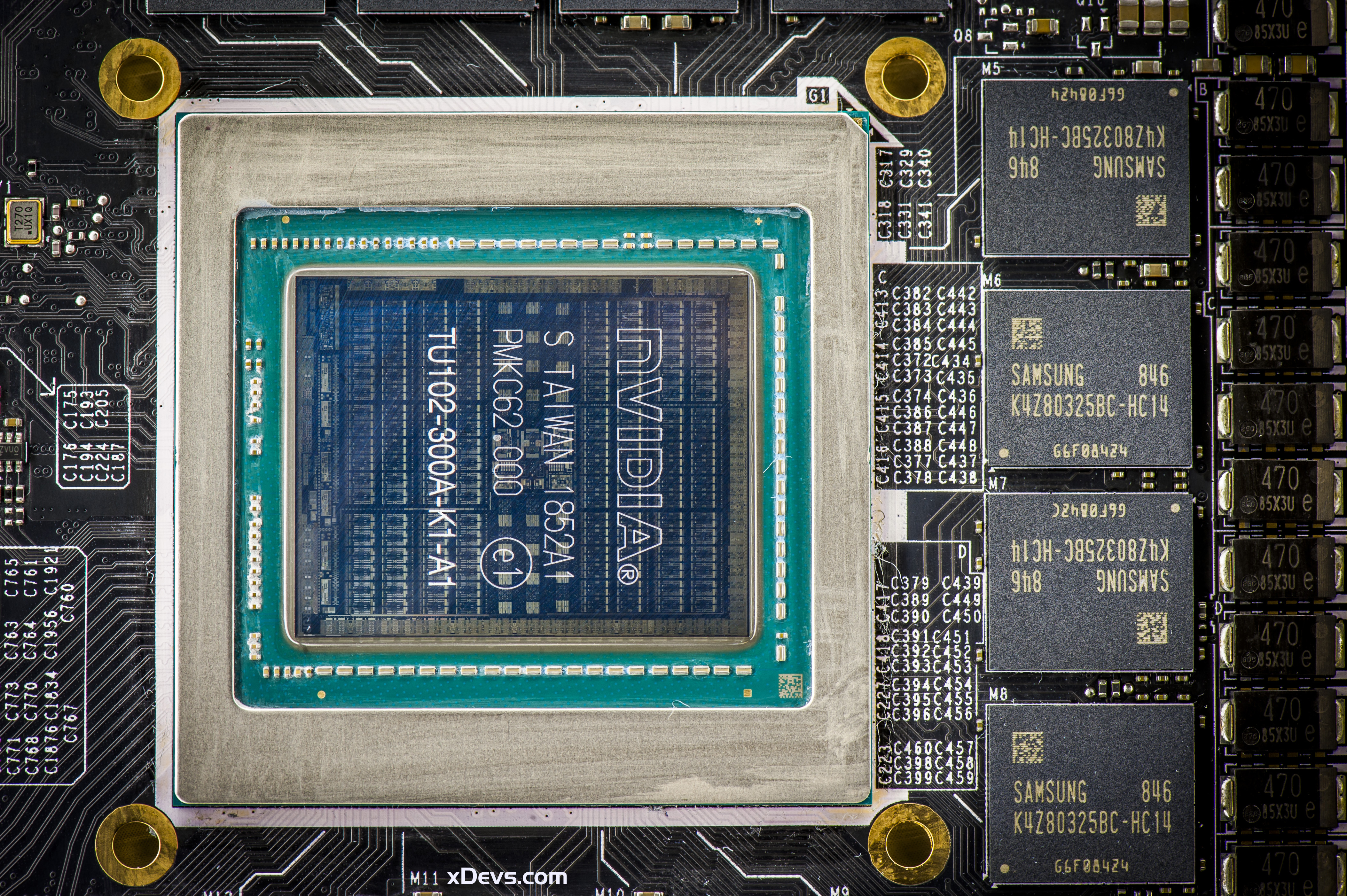
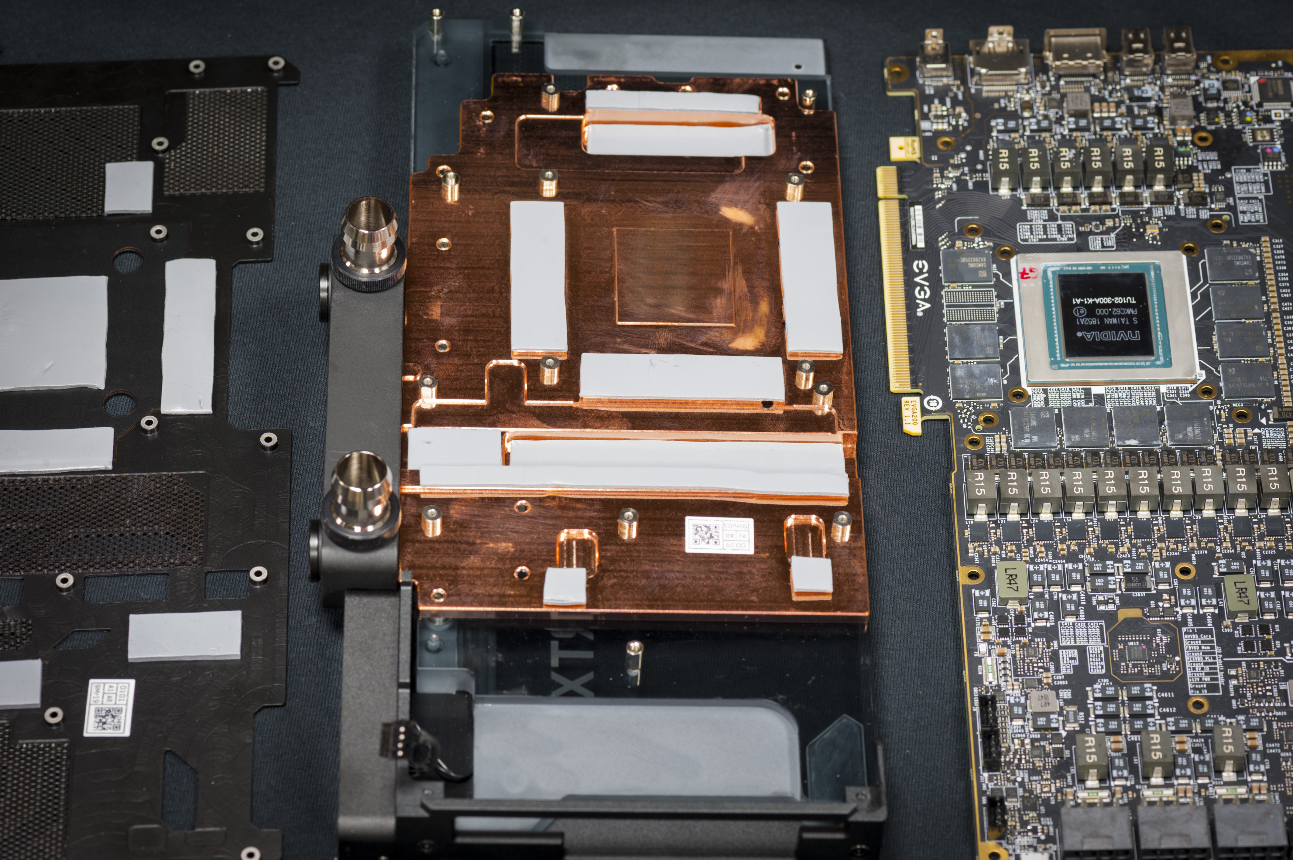
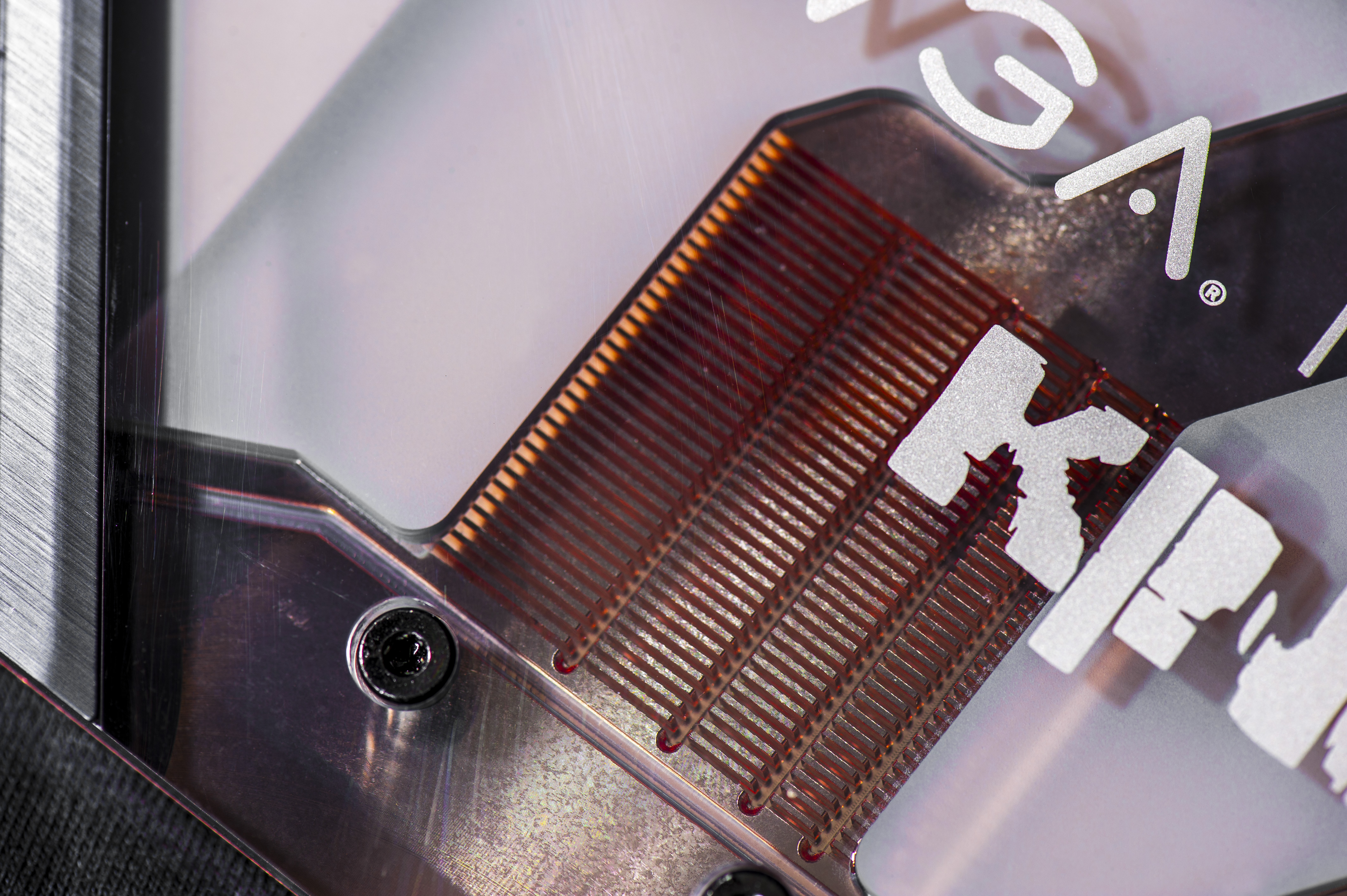
Image 2: GPU and memory under the hood
KPE RTX 2080 Ti has a maximum 2-slot width to allow more options for dense 2-Way SLI setups. More practical benefits of an increased spacing are better compatibility with packed hardware configurations or microATX builds. It is possible to find content-creation HEDT platforms with few high-speed PCI-Express SSD drives, PCIe audio cards like EVGA NU Audio or multi-port RAID HBA and 10 GbE PCIe NIC. Video content creation in VR and high-definition 4K/5K or even 8K resolutions systems demand the highest performance available.
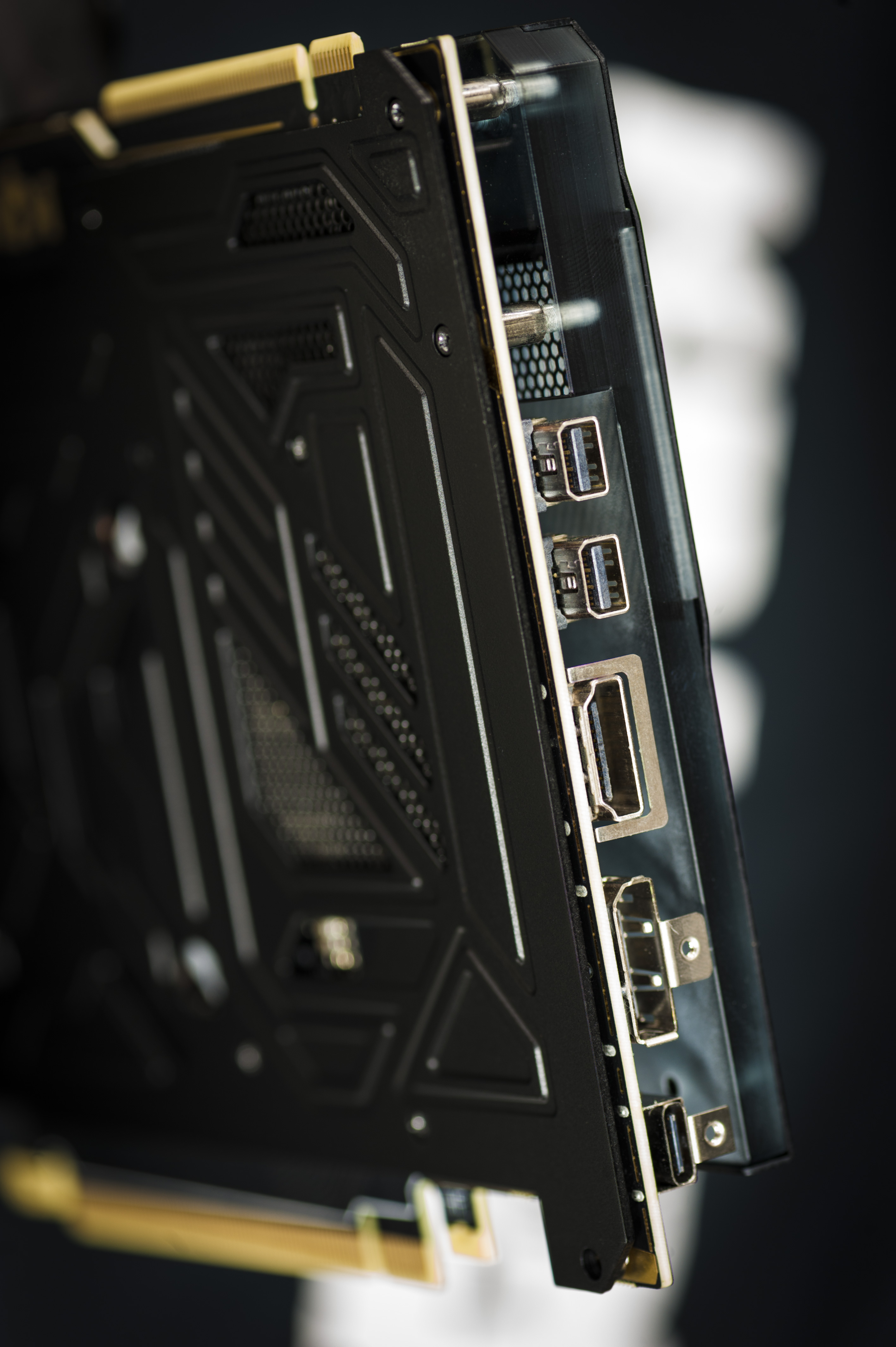
Front I/O connections follow the similar layout as on previous cards of this series, featuring full support for Turing TU102 available outputs. Any four outputs can be used simultaneously from one card and the card is bundled with some miniDP passive adapters.
- 2 x Mini-Display Port 1.4a ports.
- 1 x full-size HDMI 2.0b with HDCP 2.2 port.
- 1 x full-size DP 1.4a port
- 1 x VirtualLink USB Type-C port with USB 3.1 Gen2 host functionality.
All DisplayPort interfaces support DSC 1.2 and can drive 8K panels at 60 Hz refresh rate. DP ports can even do two displays 8K/60Hz each, using one DisplayPort HBR3 cable using DSC when daisy-chained with supported devices.
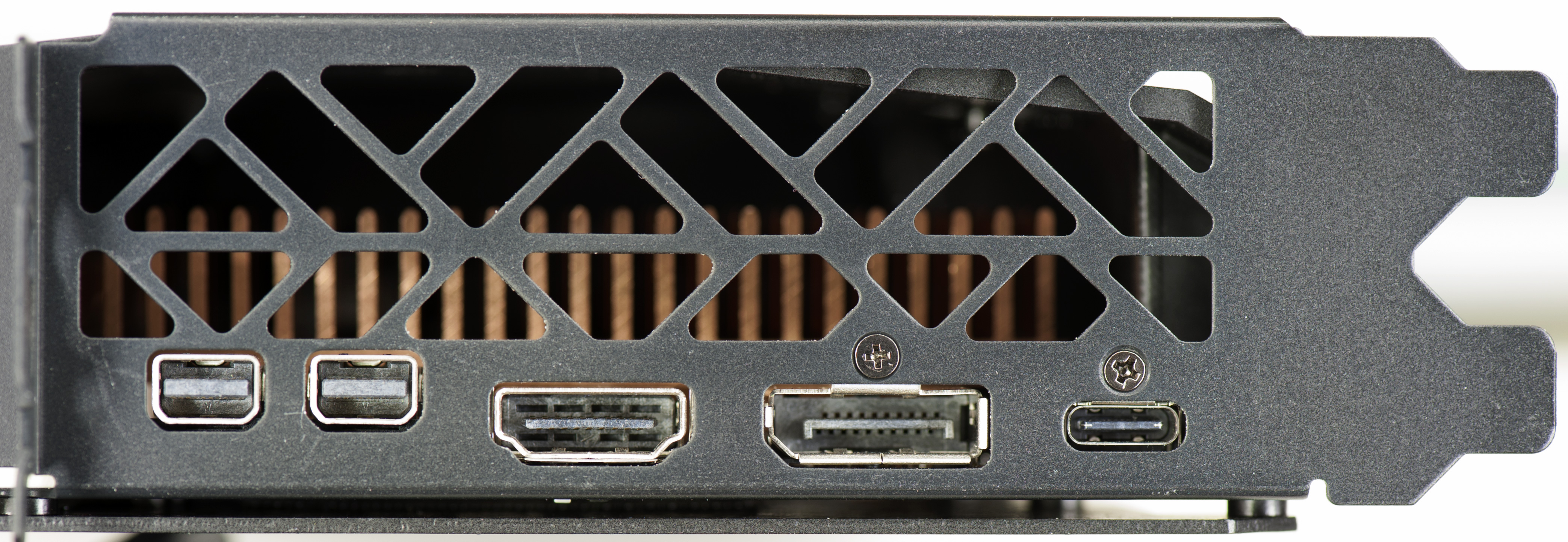
Image 3: I/O interface bracket with all display output ports
Turing GPUs do not have RAMDAC and analog signaling VGA circuitry anymore, so there is no support for passive analog VGA adapters. If you really need analog VGA connectivity you can do so by using a more expensive active dongle.
Custom backplate is stock on all KINGPIN RTX 2080 Ti cards. It covers the rear of the circuit board with thermal pads both behind the GPU core and GDDR6 memory areas to avoid heat being trapped under the solid metal cover. Backplate is mounted to the card and fan-sink baseplate by using 18 small Philips-head screws.
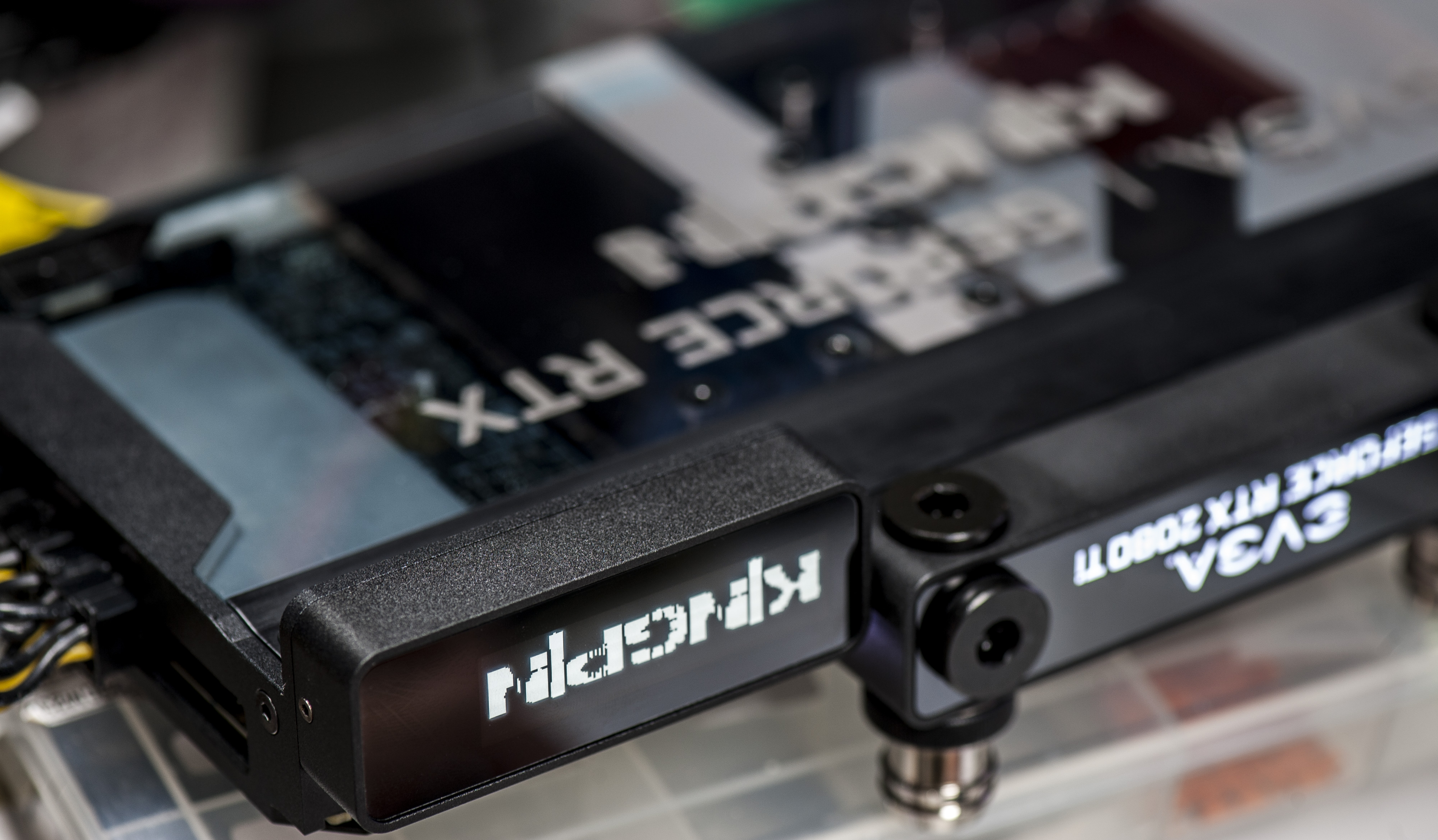
Image 4: OLED screen on Hybrid cooler top surface
Display is black&white OLED, with graphics dot matrix, capable of displaying images up to 256 × 64 pixel. It’s used for self-test diagnostic information (when card detects wrong voltage levels or power issues) or monitoring information like frequencies, voltages, temperatures. It can also customizable to display user bitmaps or text messages as well.
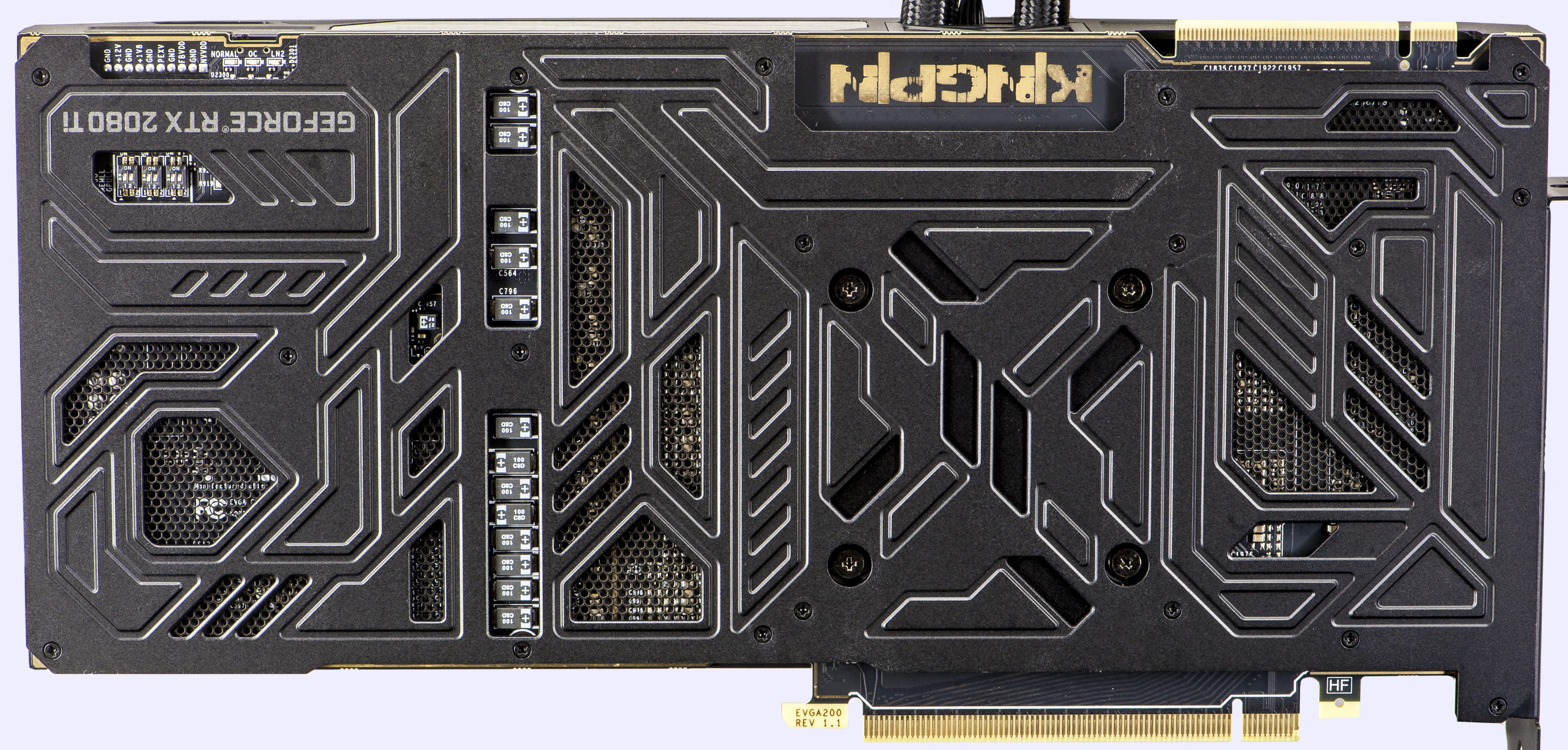
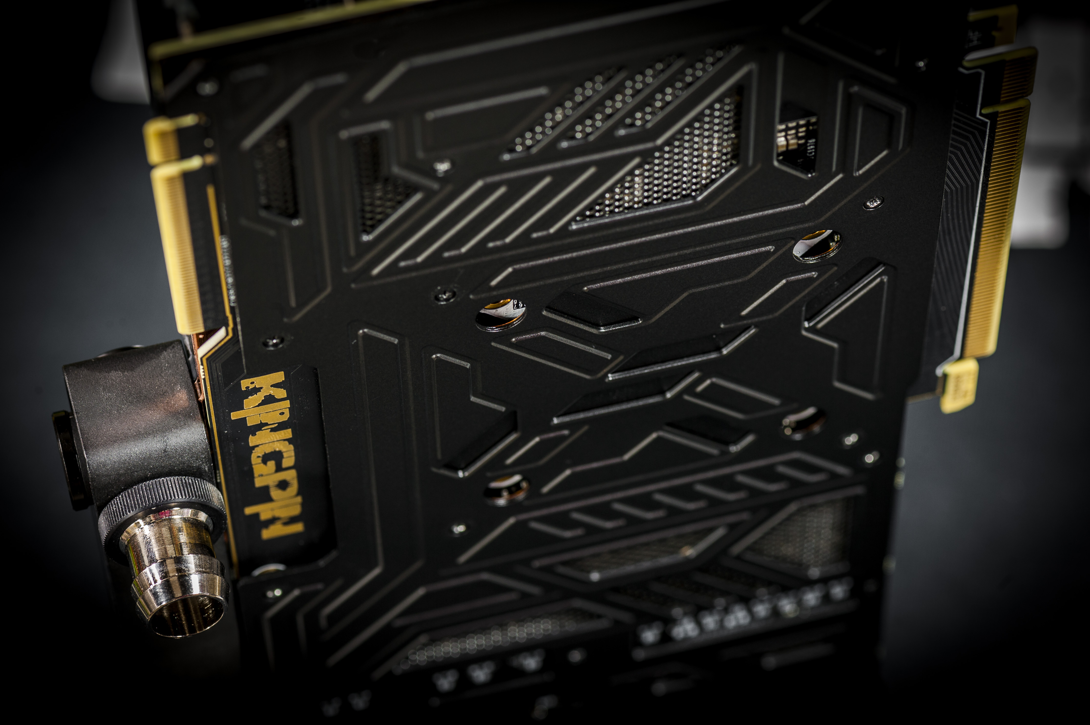
Image 5: Backplate on RTX KPE card
The metal backplate has a dual purpose, acting as protection cover and heatsink. Thermal pads located behind GPU and VRM components help to transfer some of the heat into the backside of the board. There are no fancy bling LEDs anywhere on the back, except three dim indicator LEDs for BIOS switch position.
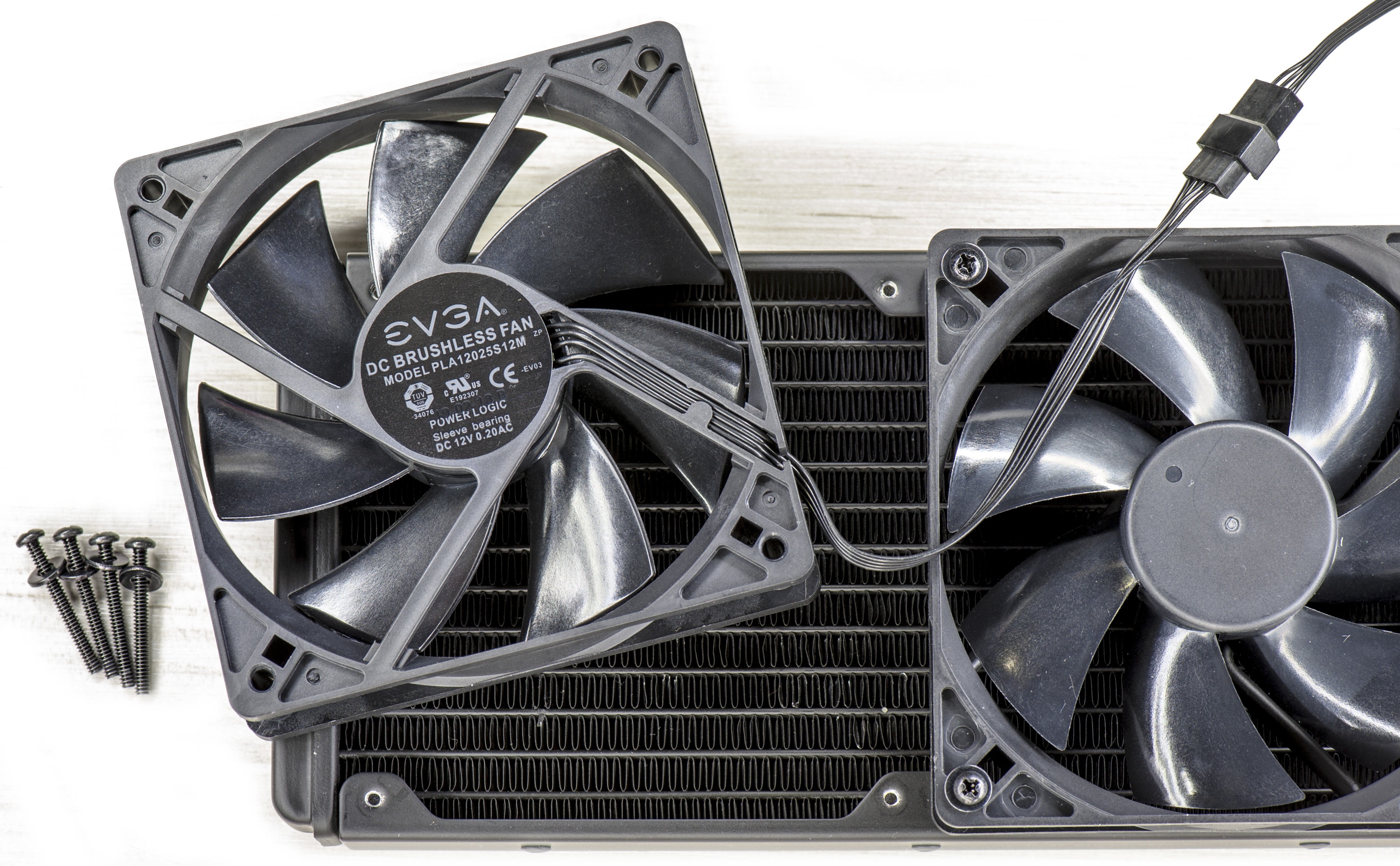
Image 6: Asetek Hybrid radiator and used DC fans
Dual radiator equipped with two 120×120×25 mm PWM fans, made by Power Logic for EVGA. A radiator has mount holes for standard 120mm fan from both sides. If you desire best cooling performance fans can be replaced with higher speed fans. Also, 2 additional fans can be installed on the other side of the radiator to provide push-pull airflow. Maximum current supported by radiator fan power connector is 1.2 A combined.
If you need higher than 1.2 A (14.4 W at +12V), please use an external fan header or headers from motherboard / standalone fan controller.
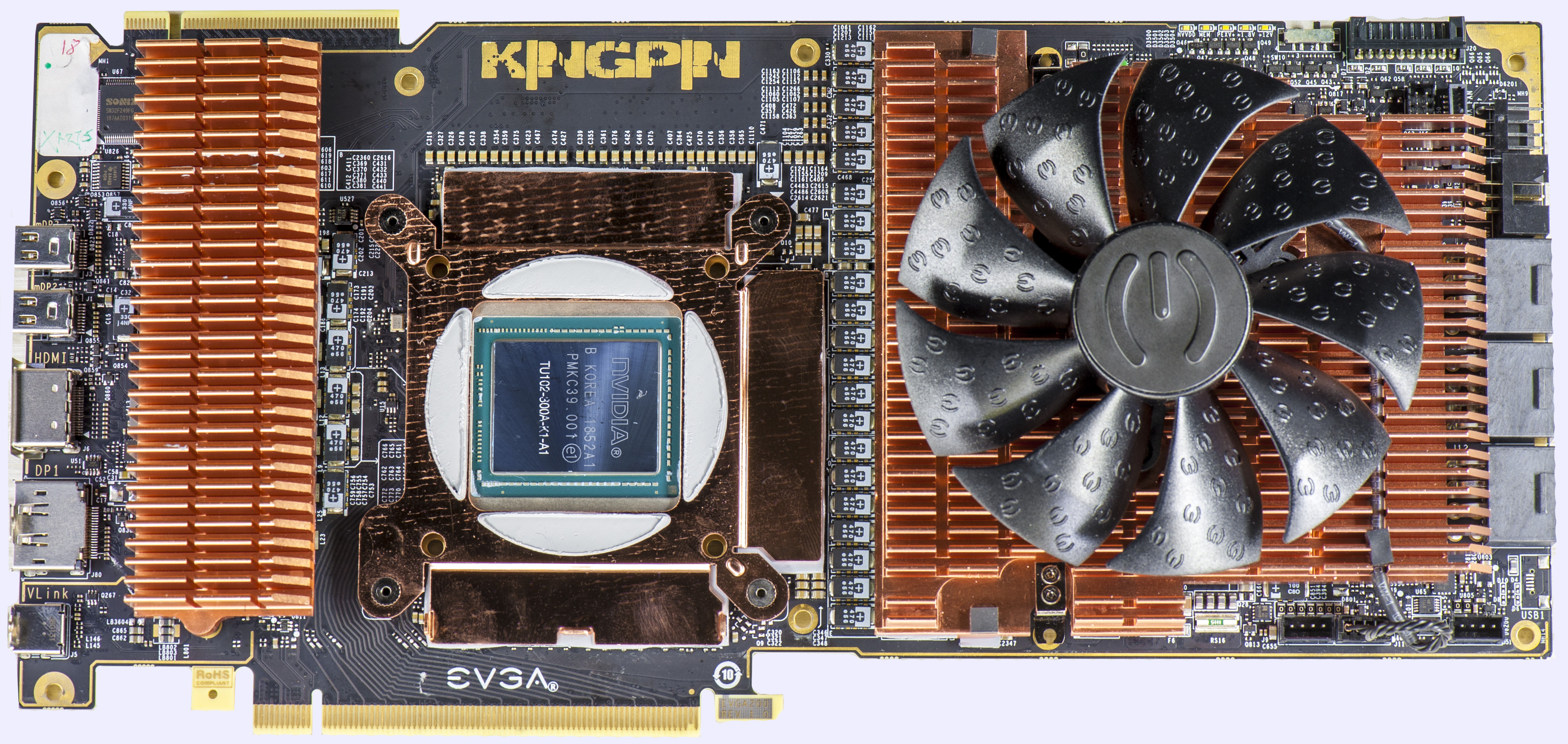
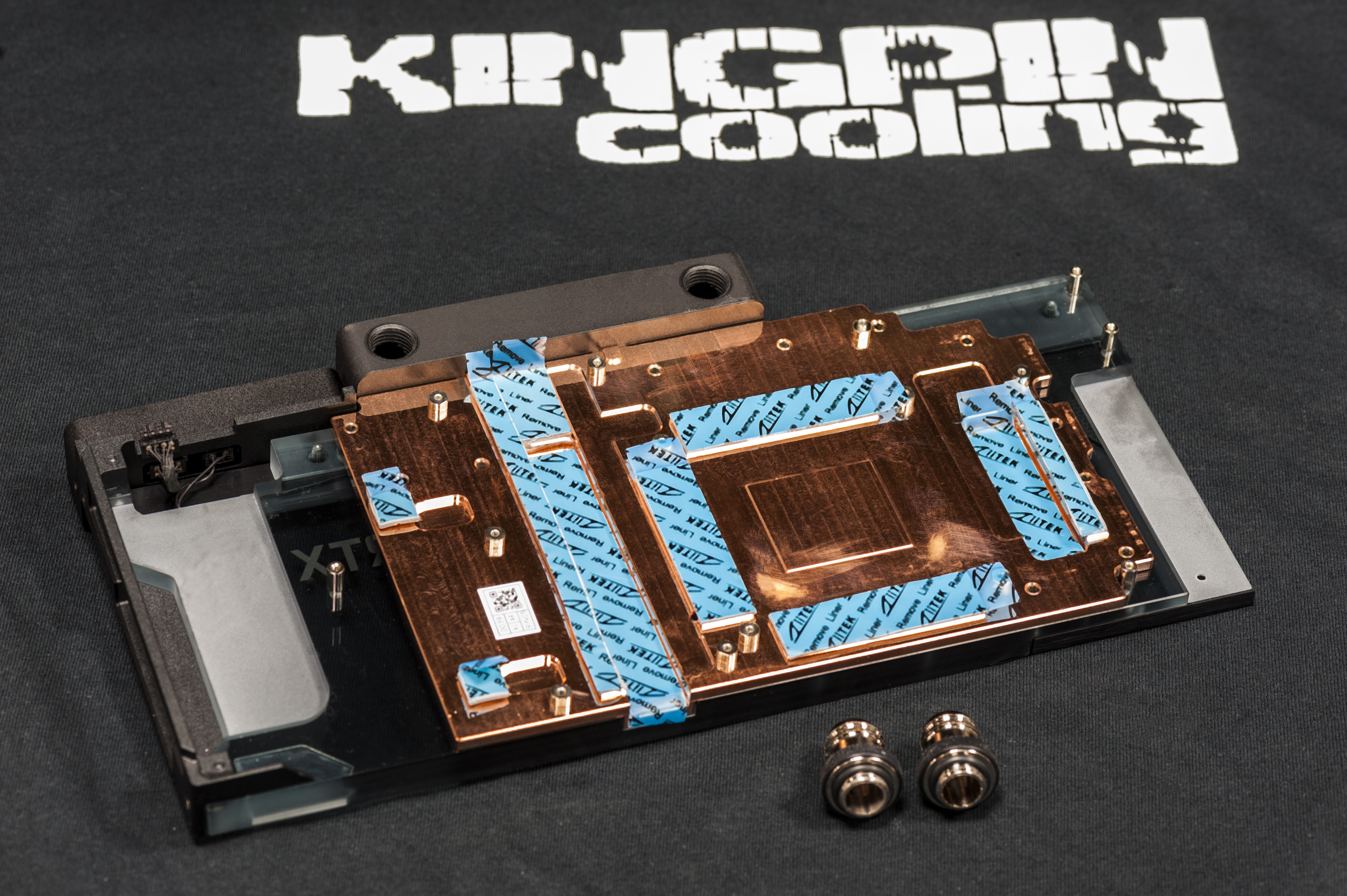
Image 7: Card with removed Hybrid cover and Asetek pump assembly
Removal of the cooler requires undoing small screws on the backplate and four GPU cooler spring screws. Then metal cover and heatsink comes off straight up. Modular VRM heatsinks are independent of heatsink cover / GPU cooling assembly to allow aftermarket cooling parts on GPU.
Gamers Nexus media outlet did a great detailed teardown on preproduction KPE sample.
If you looking for using 3rd party waterblock, like a chiller setup VRM heatsinks can be left in place to provide proper cooling for VRM power stages. Leaving GDDR6 memory cold plate would be good idea, in case it’s compatible with used cooler, as memory tends to get rather hot if passively cooled.
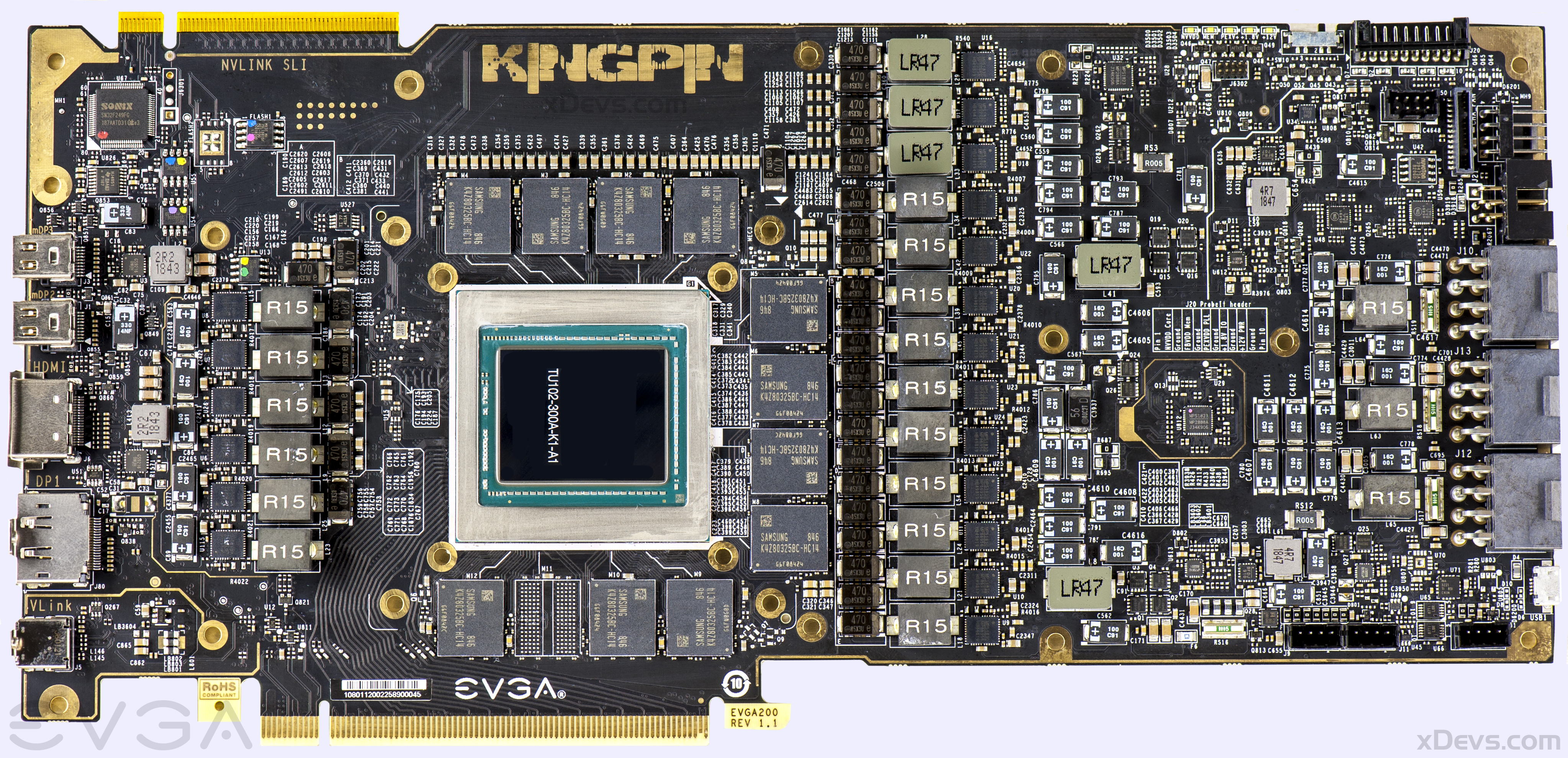
Image 8: Fully naked EVGA RTX 2080 Ti K|NGP|N Edition card, top side
Mount hole locations on RTX 2080 Ti are slightly different than the previous generation 1080 Ti and earlier NV cards. Keep that in mind when using legacy coolers. Kingpin 2080 Ti, however, follows the same dimensions and GPU location as a reference card.
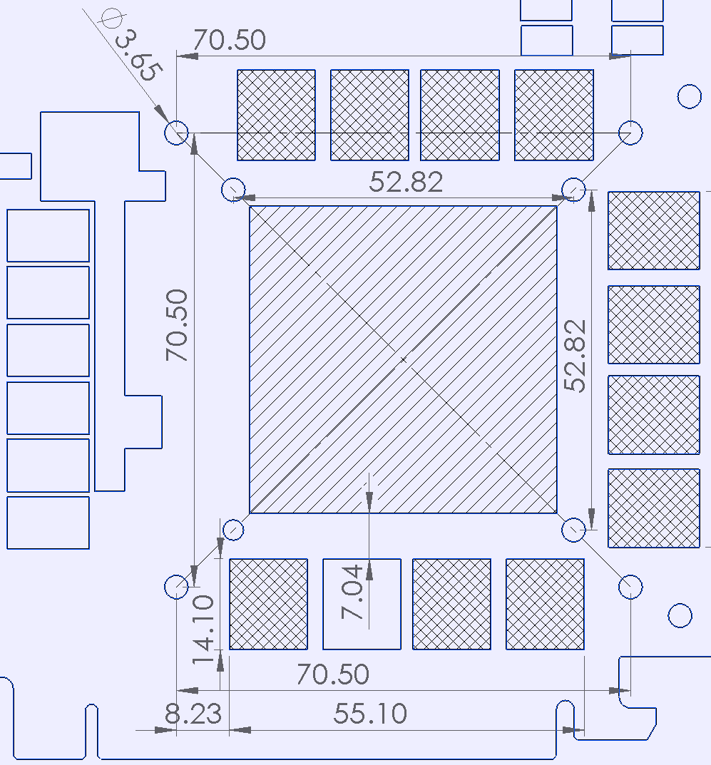
Image 9: Dimensions for cooler mounts around GPU and memory spacing.
Reason for hole location change on RTX is due to memory routing challenges. To reach high speeds new GDDR6 layout for memory IC had to be relocated much closer to GPU than previous generation graphics cards with GDDR5X and GDDR5.
What is all this VirtualLink thing?
USB Type-C Specification supports the use of Alternate Modes using the USB Type-C™ connector and cables. Various USB Type-C connector pins may be re-configured to support different interface needs, including display connectivity. One of these Alternate modes is VirtualLink whereby four lanes of VESA defined DisplayPort™ signaling and USB-IF defined USB3 signaling are simultaneously routed over a USB Type-C connector using the above repurposed signals. This is different to already existing DisplayPort Alternate mode, which provides only USB 2.0 data rates combined with DP transfer.
An existing challenge of many VR HMD is the cumbersome multi-connector cable set and/or adapters that these devices require. This challenge often sets the use of HMDs at odds with consumers’ desires for portability and simple device setup. These cables are often incompatible with particular system outputs and not well supported on new market applications, with devices like VR Notebook.
The VirtualLink Alternate Mode enables a better solution allowing a single USB-C connector to simultaneously provide a number of things:
- Up to 27 Watts of DC power to provide HMD power
- Up to four high-speed DisplayPort lanes to accommodate growing display resolutions
- Bi-directional USB3.1 Gen2 SuperSpeed data channel for HD cameras and other sensors found in such devices.
- Streamlined lightweight single cable between devices
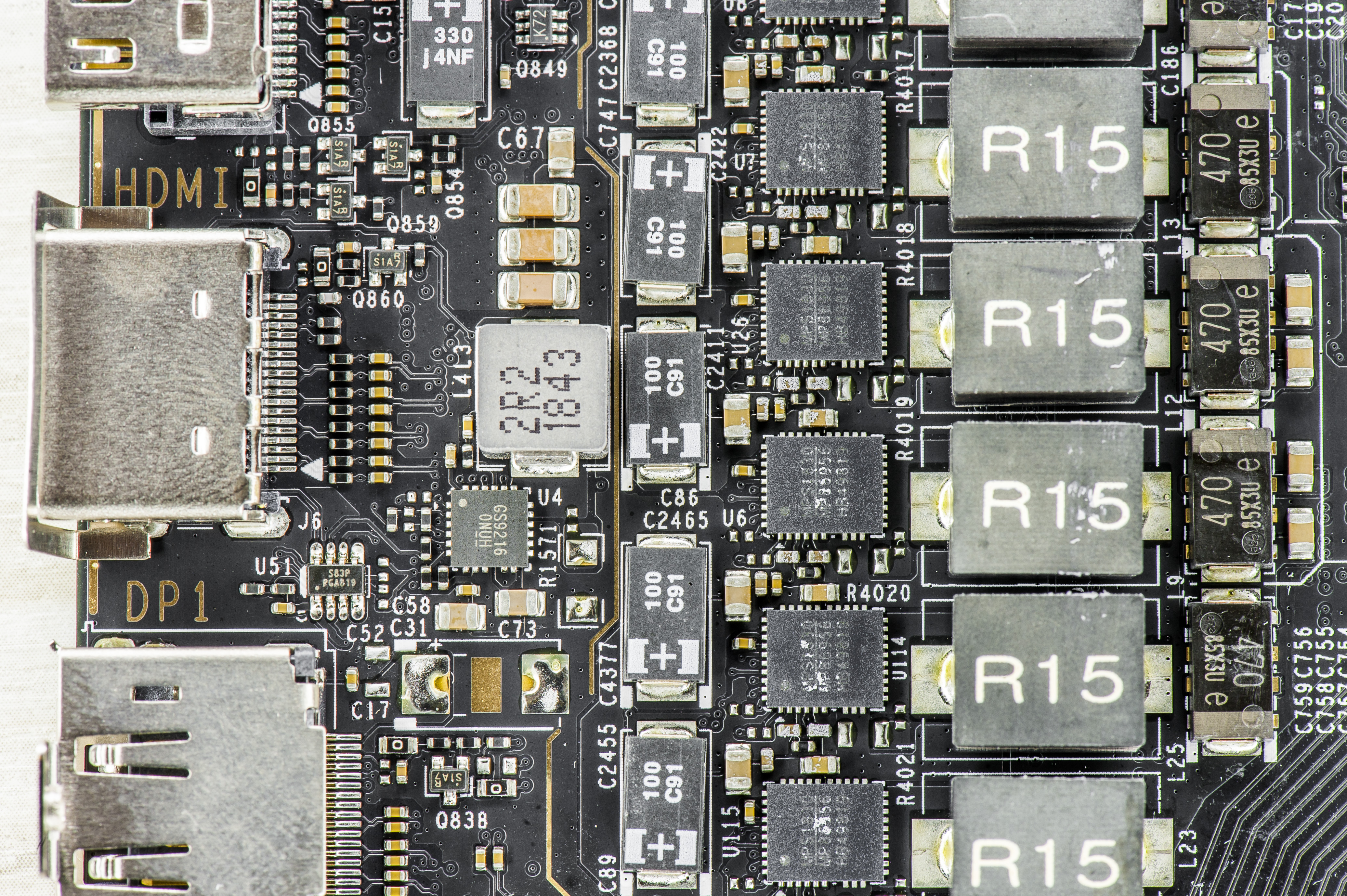
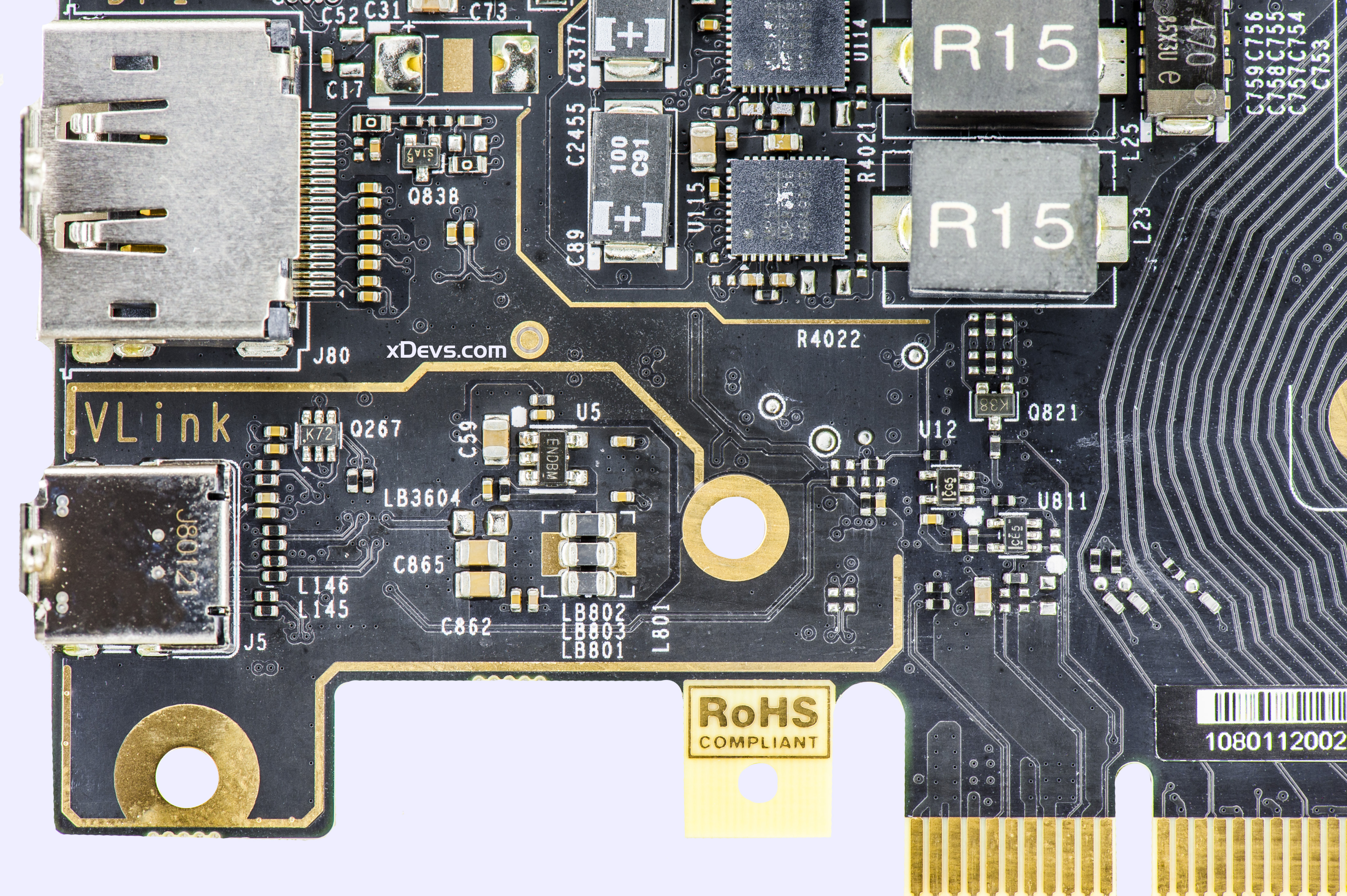
Image 10-11: VirtualLink™, HDMI and DisplayPort™ interface ports
When a source device such as RTX 2080 Ti-based graphics card enters the VirtualLink Alternate Mode, the USB 2.0 interface is dropped from the USB-C connector. HMD devices of two power classes are supported:
- 15 W Power Class HMD that is capable of using up to 15W (5V × 3A) on USB Type-C VirtualLink port
- 27 W Power Class HMD that is capable of using up to 27W (12V × 2.25A) on USB Type-C VirtualLink port
Keep in mind, VirtualLink is supported only on Captive USB Type-C specially designed cables. A captive USB Type-C cable is a cable where only the graphics card source side exposes a USB Type-C connector (the HMD side must either be permanently soldered to the HMD or be exposed via a non-standard USB Type-C connector). This is a result of difficult signaling requirements for VirtualLink mode, to prevent end-user problems when VirtualLink graphics card and VirtualLink HMD interconnected by non-complaint standard USB Type-C cable.
Support for VirtualLink functionality requires updated OS, which is currently only Windows 10 Fall 2018 Update or later version. RTX cards equipped with VirtualLink also get NVIDIA USB Type-C driver installed, so you can also use VirtualPort as standard USB Type-C host port.
GDDR6 Memory and its overclocking
In modern games and benchmarks like 3Dmark Time Spy or Port Royal graphics memory overclocking is just as important as the GPU OC or even more so. Our pretesting on multiple RTX 2080Ti Kingpin samples revealed expected overclocking offsets on used Samsung GDDR6 memory at +1000 MHz over the specified 7000 MHz (14 Gbps effective with DDR), with some cards going all the way to +1500 MHz on memory frequency offset when maxed out. Memory performance during the card design was one of the key aspects for delivering reliable performance balance from both GPU and memory domain.
Since GDDR6 memory is now provided by multiple manufacturers, with RTX 2080 Ti KINGPIN EVGA is going back to traditional Samsung K4Z80325BC-HC14 memory chips, in standard 11 GByte configuration. These chips are rated for 14.0 Gb/s data rate and designed for 0-85 °C temperature range running at nominal 1.35 VDDQ ±3%. Maximum stable memory frequency can scale a bit with memory voltage, especially when well cooled.
This means that if you provide a slight bump in memory voltage, at around 1.45-1.50 VDC, you may be able to squeeze a hundred or two more MHz on memory clock without losing benchmark stability. When you are overclocking on LN2, you want to match the highest GPU core clock + highest memory clock before performance and benchmark score start throttling/decreasing. Maximum clock is not always translating into the best score. When overclocking hard GPU can detect minor data errors on the memory and repeat data transfer to retry. Result of this is increased latency and performance throttle, that can be detected as lower scores when raw frequency set by the user is actually higher.
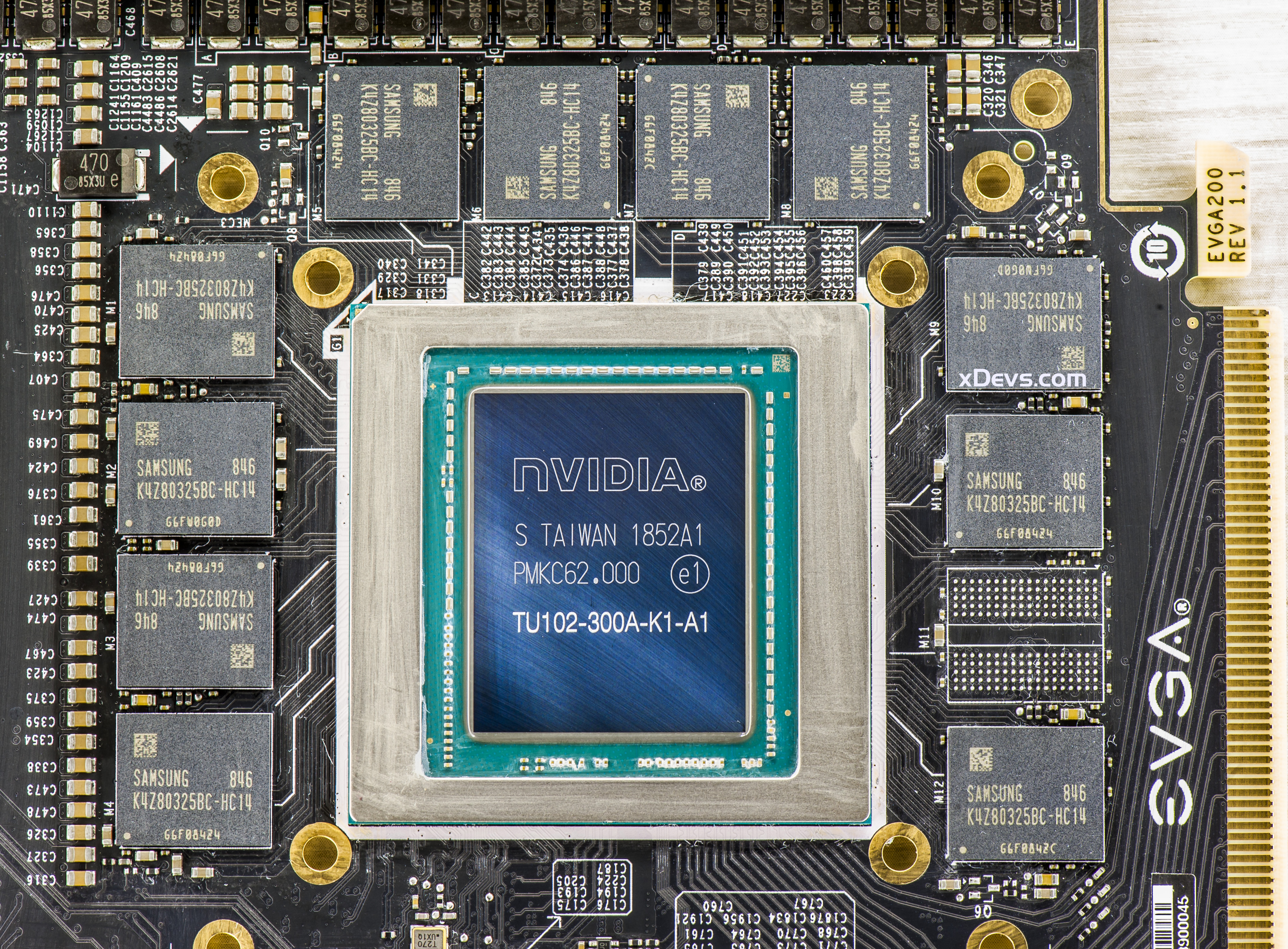
Image 12: RTX 2080 Ti KPE memory layout and Samsung IC photo
Also elevated memory voltages help to keep the GPU’s memory controller from flaking out on extreme cold thus limiting max memory OC. Keep in mind that the card’s memory is calibrated and trained when it initializes and the boots windows. Sometimes when raising memory voltage higher for example to 1.55 V in one big step while at idle desktop, it can cause the GPU to lock and artifact. This is normal and happens because the memory has already been calibrated at a lower voltage long before you got into OS, and now need re-calibration. A simple reboot without resetting desired voltage is all that is needed in such cases. Everything will be working fine on next boot into windows with already raised memory voltage.
Please note that running high voltages (hint: over 1.55 V) on your cards memory for extended periods of time (weeks, months) may degrade the IC’s slightly so this is not advised for continuous use, but rather reserved for benchmarking/competition purposes. It is always worthy to spend time finding out exactly what memory voltage your cards need to run at your desired clock so you know your hardware limits and are not running unnecessary excessive voltages without the need for it. We usually run 1.50-1.55 Vmem on cards at LN2 temps, which has proven to be a sweet spot for 2500+ MHz GPU clocks and high memory OC over 8400 MHz (QDR).
For stock water-cooling cooling, usually I don’t go over 1.50 V even if the card is able to handle that well. This is a level when increasing voltage further returns diminishing results in overclocking headroom, due to much harder stress on memory die thermals. Actual theoretical maximum voltage for this GDDR6 memory is specified at 2.0 V, which already way higher than GPU can tolerate or we may ever need.
Power target and power limits
Turing chip is pushing power envelope even further than already dense previous generation GTX 1080 Ti. To keep up with increased power demands and keeping boost clocks high we chose to use not two, but three 8-pin +12V power entry connectors. These are standard MiniFit Jr. type, with power limit meeting NV’s spec at 150W per port. As a result this allowed specifying higher power limit levels for VBIOS, so the performance of GPU is not limited by power. Essentially using this design allow KPE GPU to run at maximum boost clock, limited only by the temperature and cooling performance.
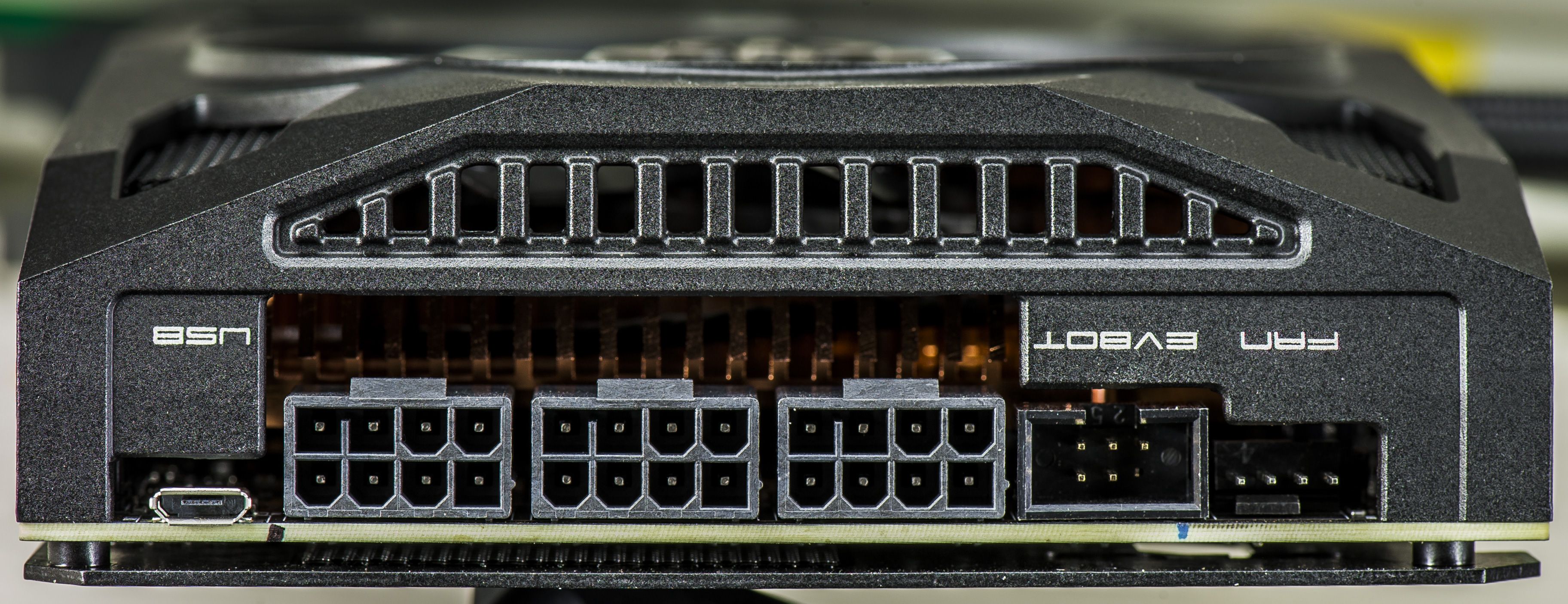
Image 13: Rear card side with micro-USB, 8-pin power connectors, EVBOT and external PWM Fan headers
TGP or more typical term “power limit” is the main item to handicap performance in favor of thermals. Every NVIDIA card since the Kepler generation has a power limiter and special associated circuitry on the PCB to measure and allow GPU to regulate input consumption. This control traditionally does not report you any amps or Watts value but instead provides a percentage over design specification (which often varies depending on card SKU/BIOS/vendor!). Attempts to compare 144% limit value of card A to 106% value of the card B will give you no useful information without the knowing actual power limit for each SKU. Card B in such case could have stock (100%) power spec 400W, while card A rated at lower 260W.
Often owners and users are referring to 6-pin or 8-pin input power MiniFit.JR type connectors as 75W or 150W capable inputs. That is not the complete truth. These power numbers are nothing but just logic programmed values for NV to determine how capable is used board hardware to deliver high power. It’s a purely imaginary number and has nothing to do with actual real power rating from connector nor true power input capability. Software and NV BIOS will handle GPU clocks and reduce voltages if measured power hitting programmed BIOS limit (which can be a different value than 75/150W!).
Anyone can confirm this by looking at manufacturer specification limits of power connector itself, such as Molex 26-01-3116. These are rated from 13A per contact (16AWG wire in small connector) to 8.5A/contact (18AWG thinner gauge wire).
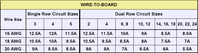
Image 14: Molex 26-01-3116 MiniFit-Jr. current rating specs.
This means that using common 18AWG cable from PSU, 6-pin connector as result specified for 17A of current (3 contacts for +12V power, 2 contacts for GND return, one contact for presence detect). Bigger 8-pin have 25.5A current specification (3 contacts for +12V power, 3 contacts for GND return and 2 contacts for detection). High-end PSU usually have 16AWG wires for graphics power cable which translates into 240W or 360W power specification for 6 and 8-pin accordingly. This is given a connector temperature raise of 30 °C with all power pins used. With active airflow and decent cable quality, safe current limits are even higher.
Now if somebody states “8-pin can’t provide more than 150W”, we now know that’s not exactly correct. It is not the connector itself or cable limit the power, but active regulation of GPU/BIOS/Driver according to the detection of used cables and preprogrammed limits. So how actual power measured?
This card follows standard design requirements and just like most other RTX 2080 Ti have onboard ON Semi NCP45491 power sensor IC, which is quad-channel monitor able to measure voltage, current and power on +12VDC input rails using just a few external components and current shunts.
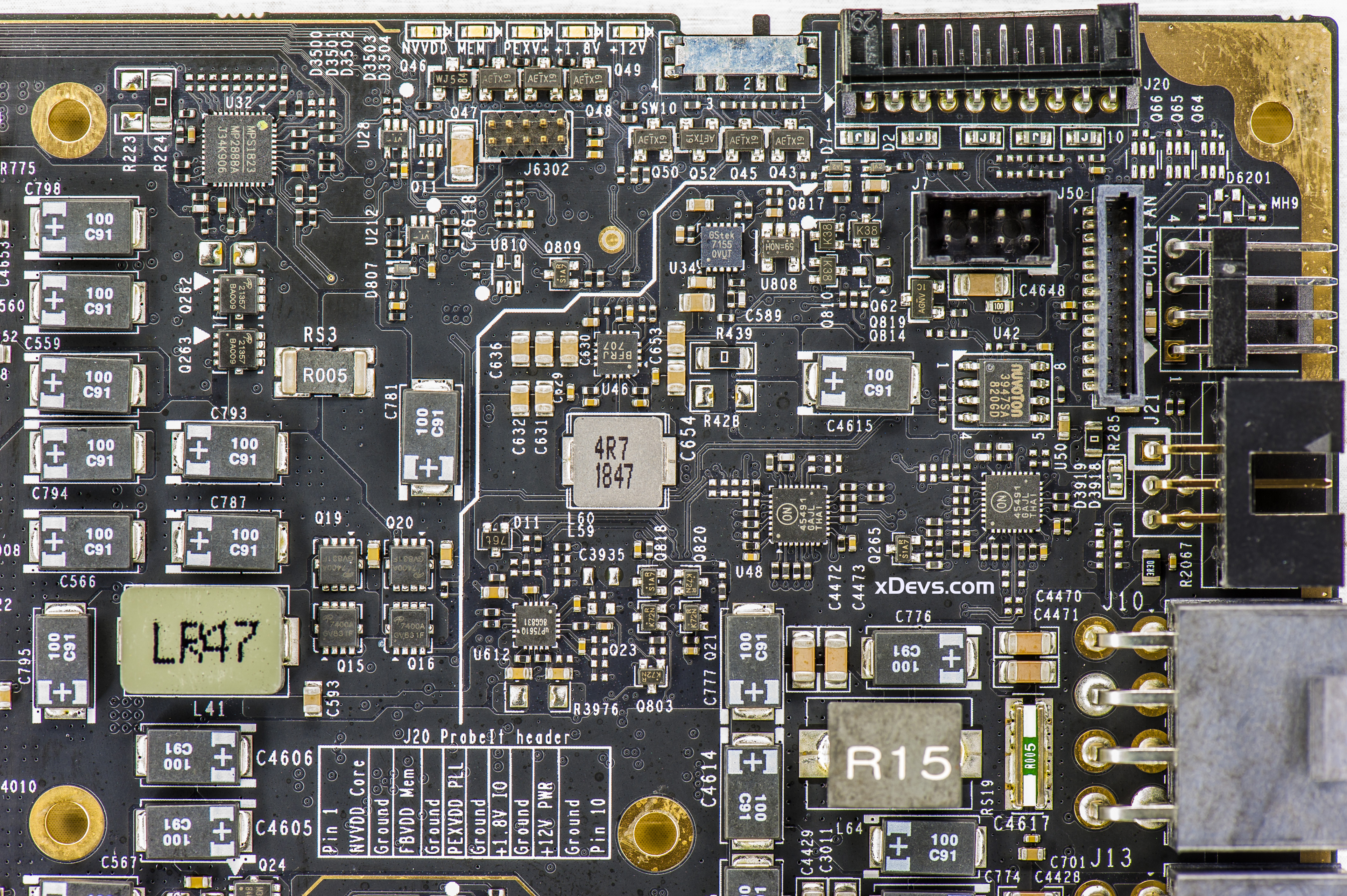

Image 15-16: Auxiliary power circuitry on KPE PCBA
Current shunt is a special type of resistor which generates little, but measurable voltage which closely depends on amount of current flowing thru it. Thus card can detect power consumption in real-time and adjust its clock speed and performance automatically to keep power within the specified envelope.
However, KPE RTX 2080 Ti designed in a way that does not require any additional power limit modifications or thermal protection removal mods. You don’t need to solder anything on the card to enjoy LN2 benchmarking with KPE. That is what this card is all about. It can overcome the power limit or any thermal limit with a proper BIOS. It is 100% designed to run at full LN2 speed without even touching the soldering iron.
Cards overclocked with LN2 and running 2500+ MHz, can take some serious power. Ensure that the PSU is at least 1500W and adequate for the job. Typical middle range 1200-1600W 80Plus Gold rated PSU should do the job well. For extreme overclocking we highly recommend running the system (CPU, peripherals, fans, motherboard) from one PSU and the VGA card from a separate second PSU with at least 90 A of current available on +12V rail.
If you’re using two power supplies make sure to turn on “VGA” power supply always first and turn off last. This is to ensure proper boot and power sequence order when using multiple PSUs. This is not an issue for standard single PSU system.
Why my card is not reaching maximum power?
Now that we know a little more about power metering, time to explain power limit setting. Power reading shows energy consumed by GPU over time when it’s busy doing the work. I could write the whole page of text trying to explain all details about how power is metered on GPU like KPE RTX, but using a practical example with real data perhaps is a better idea.
For this test, we will use oscilloscope, special high-current probe, and voltage probe to tap +12V level for power calculation. Test system specifications and details provided in Table 1.
| Graphics card | Retail EVGA RTX 2080 Ti KPE, Hybrid cooler |
| VBIOS used | LN2 position, 90.02.30.00.79 |
| Fan speeds | 100% both radiator and VRM |
| Processor | Intel® Core™ i9-9900K, 5 GHz |
| Motherboard | EVGA Z390 DARK |
| DRAM | 2 x G.SKILL F4-3600C16D-16GVK |
| Storage | Intel 760p 256GB |
| PSU | EVGA NEX 1500W Classified |
| Benchmark | 3Dmark 1.1, 2.5.5029.64 |
| Oscilloscope | Tektronix MDO4054C |
| Current probe | Tektronix TCPA300 + TCP303, rated up to 150 A, 15 MHz |
| Voltage probe | Tektronix P6251 Differential probe, rated up to ±42 V, 1 GHz |
| Precision X1 | Version 0.3.15.1 BETA |
| VGA card firmware | Version 2B.FA.38 |
Table 1: Power measurement demo system specification
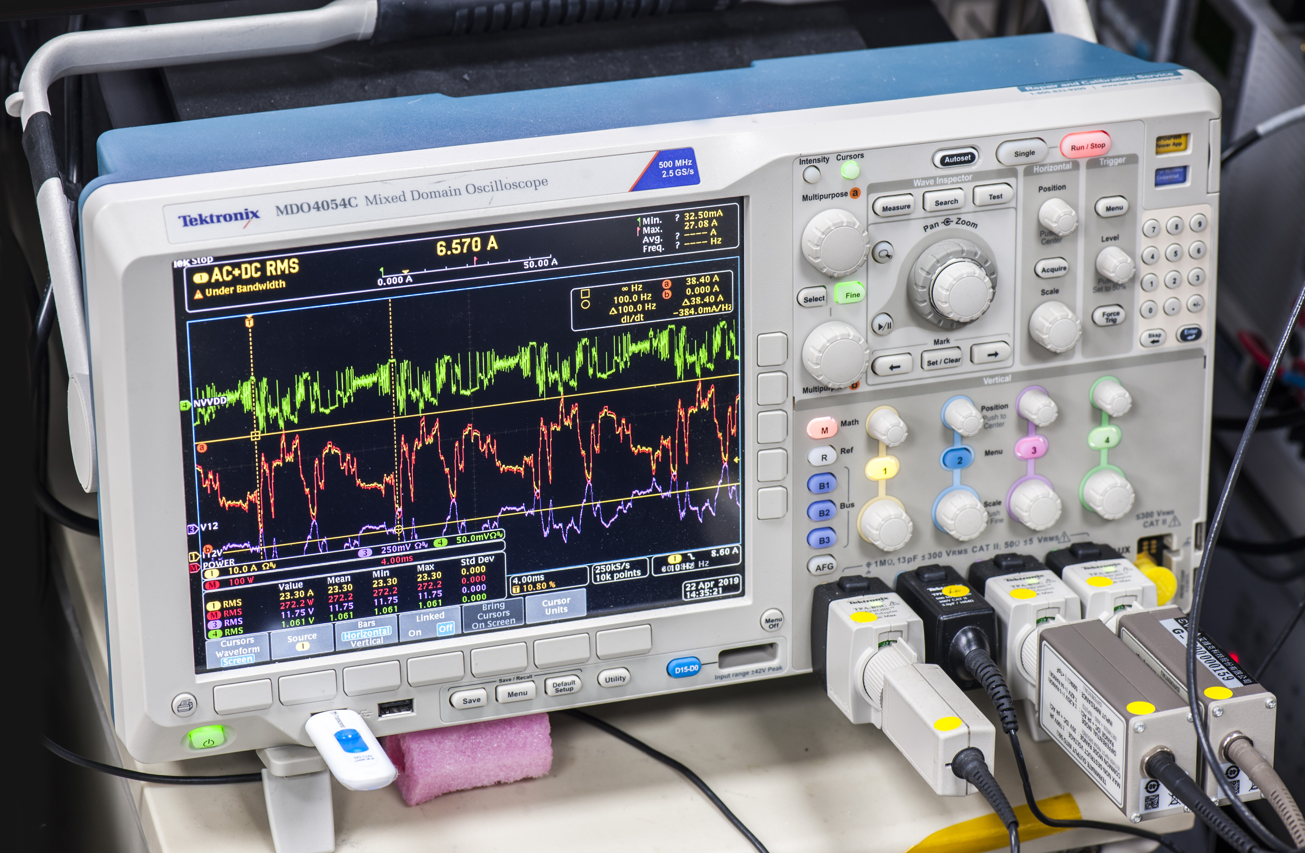
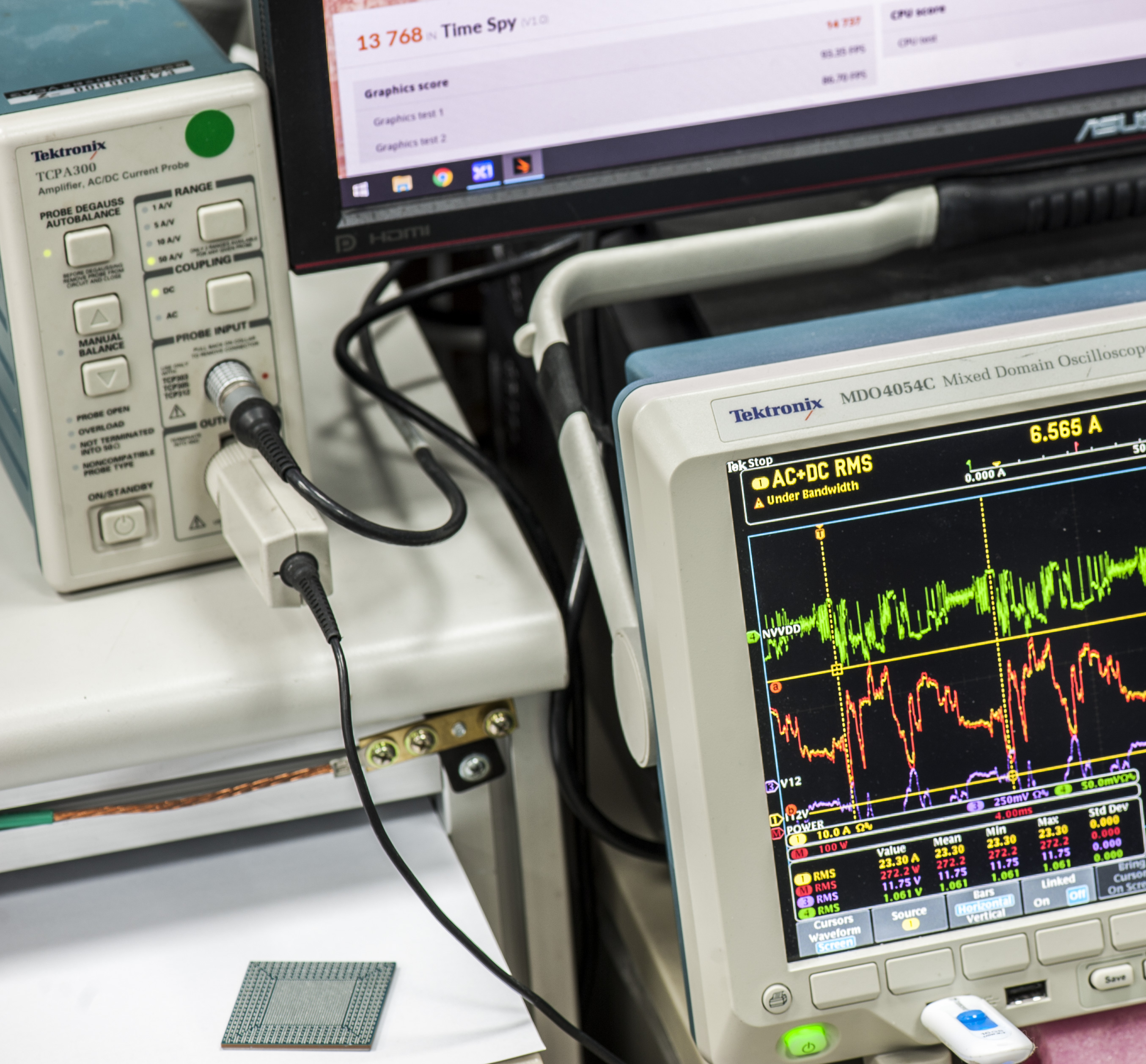
Image 17-18: Measurement scope with attached probes
During all power tests we are measuring current flowing into card thru 8pin +12V power cables and both NVVDD GPU voltage and input +12V voltage at ProbeIt header. Power in watts calculated by multiplication +12V readout with +12V current.
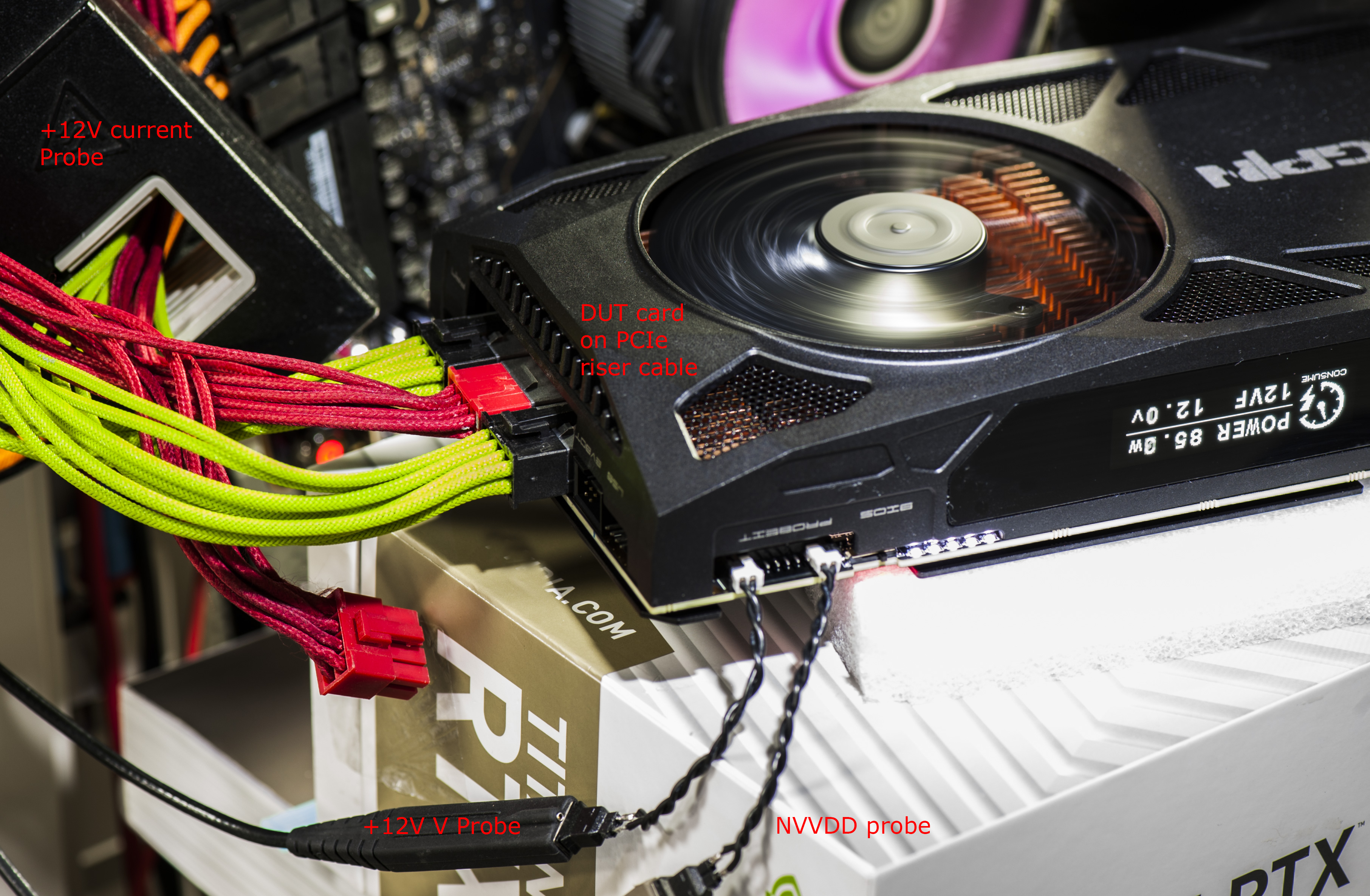
Image 19: RTX KPE under test with current and voltage probes connected
Using oscilloscope for these test allow us to detect and analyze both peak and average RMS power levels. Measuring with usual TrueRMS DMM will give only averaged values and will not show a complete picture in this case. The card was configured with LN2 BIOS to allow maximum fan speeds during all tests. Current measurements have small error due to excluded +12V PCIe slot power. Power taken from PCIe slot is not significant in tests below, so this error estimated to be below 10%. OLED readout includes power from all three +12V input power plugs as well as PCIe slot.
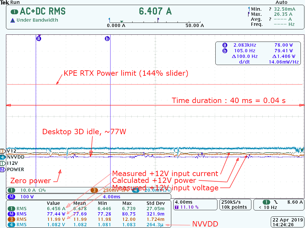
Image 20: Idle power measurement, in 3D state
Here we can see typical power taken by VGA card, sitting idle but in P0 3D state. Time scale is horizontal axis and signal amplitude level is on the vertical axis. Total time captured on graph above is 0.04 seconds = 40 ms. Scope channels are:
- Channel 1 = +12V current, measured at 8pin cables
- Channel 3 = +12V voltage, measured at ProbeIt pin9 and pin10
- Channel 4 = NVVDD voltage, measured at ProbeIt pin1 and pin2
- Channel M = Calculated +12V power delivered to VGA card
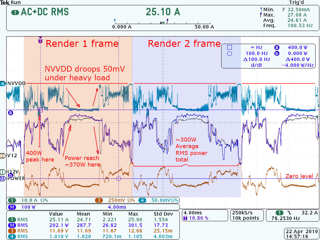
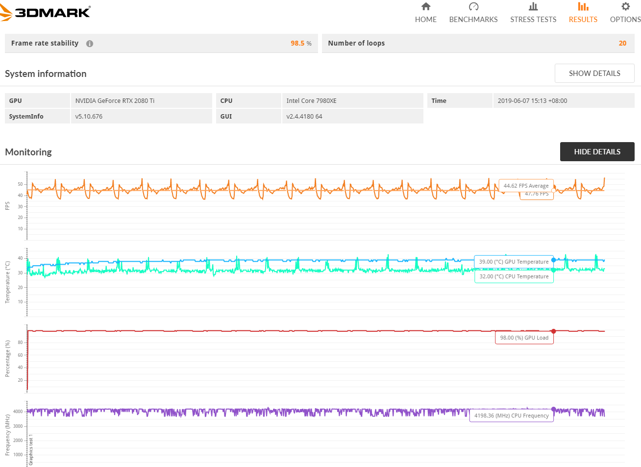
Image 21: Power readout during 3Dmark TimeSpy benchmark game scene
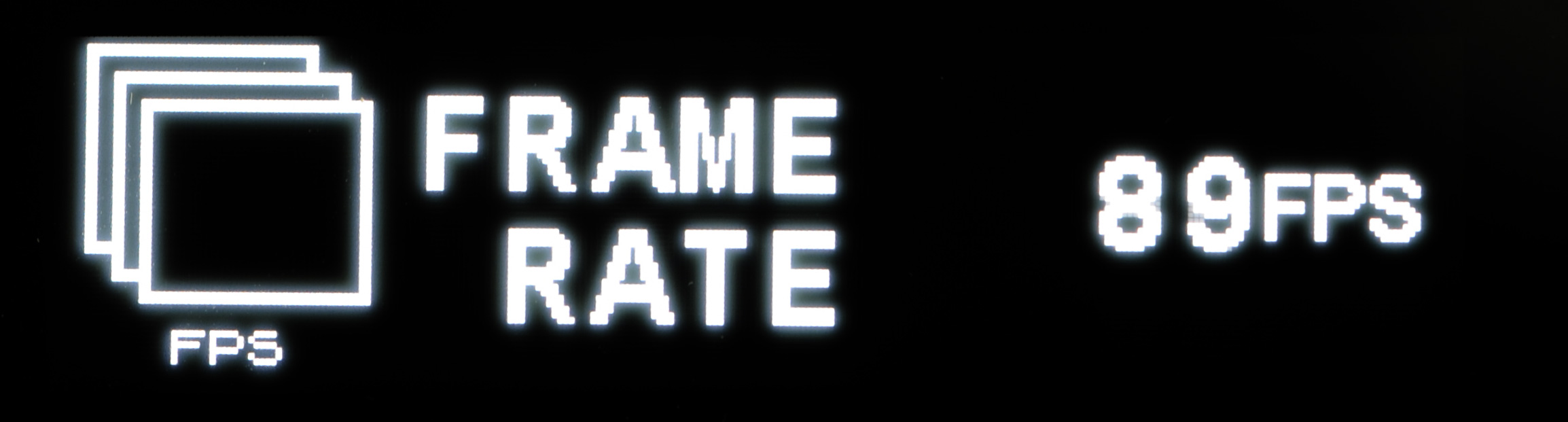
Image 21 shows GT1 test with stock voltage conditions, 2055 MHz GPU clock, 7000 MHz memory clock, 3Dmark TimeSpy. We can clearly see the repetitive waveform, which is directly related to the rendered frame. Using power measurement like this one we can even measure framerate directly from power peaks. Here frequency between peaks is around 100 Hz which is indeed matching 3Dmark ~100 FPS monitor.
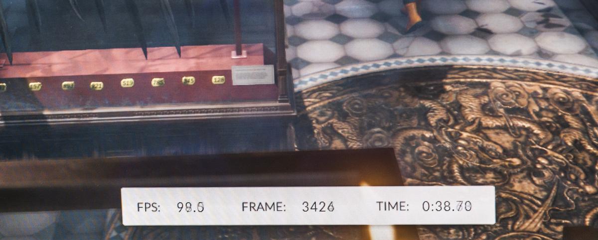
Image 22: 3Dmark framerate counter
OLED power readout matching scope results pretty close. Measurement difference varies with type of the load, by usually stays within 5-7%.

Image 23: OLED power reading
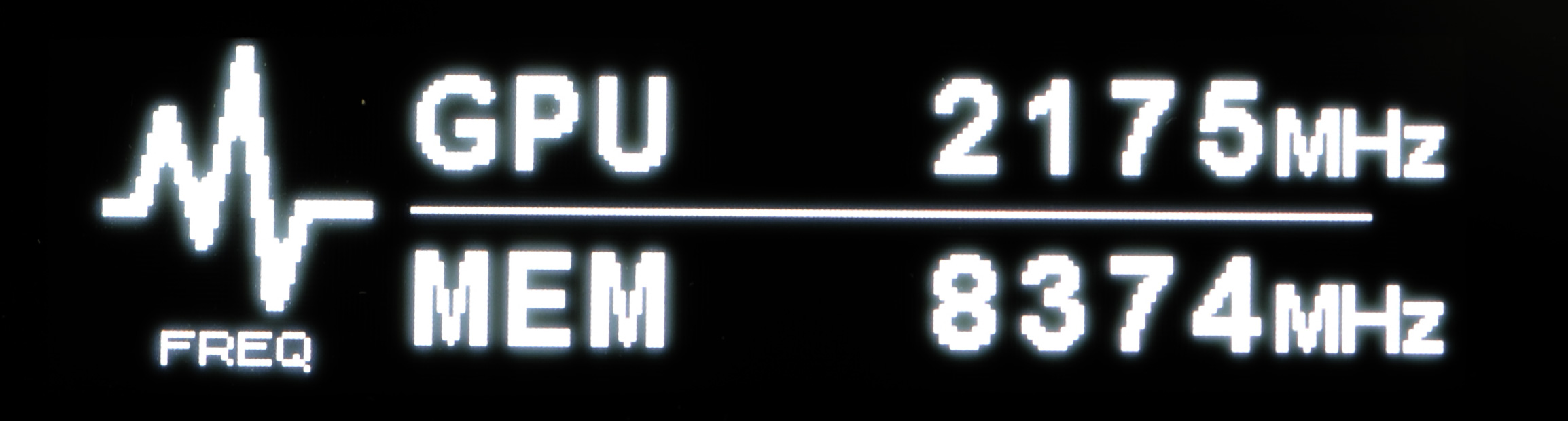
Now we can do some overclocking, set 2145 MHz GPU clock, 8000 MHz memory clock and run test again.
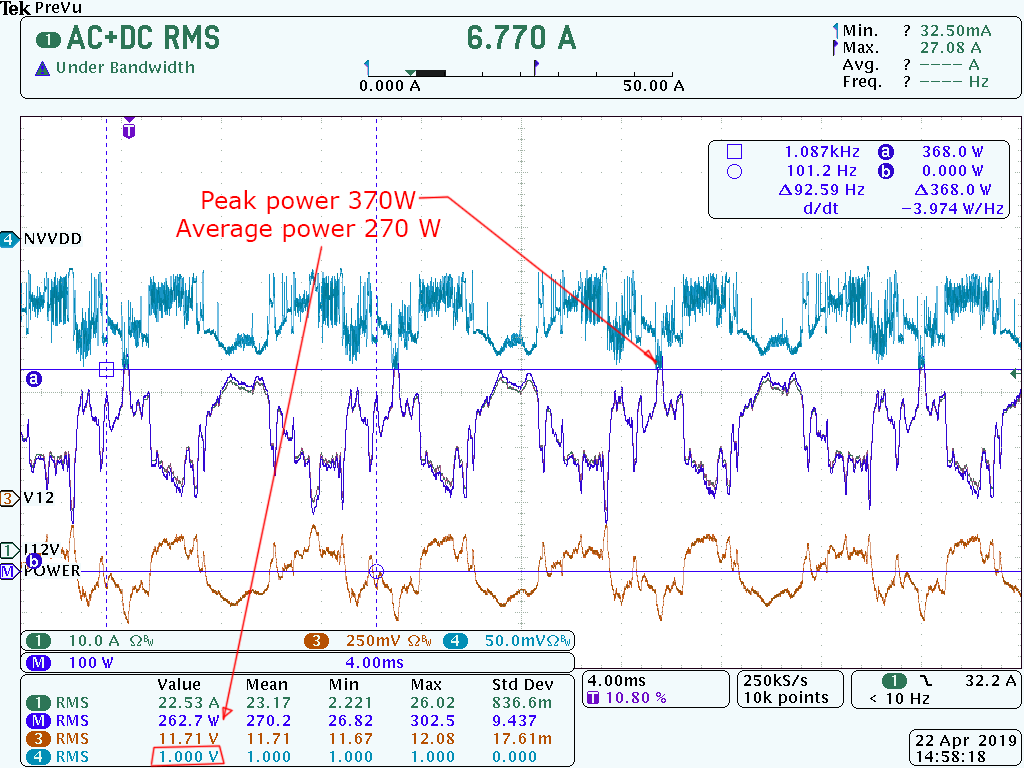
Image 24: Overclocked run with stock voltage/VRM settings
Average power barely changed, as expected. Increasing frequency does not have direct big impact on power consumption, if voltage/loadline settings left at stock settings. But there is little catch here. Because power limiter also works as peak power limit, it is not obvious when power cap is causing a hit on available performance. During overclocking / tweaking graphics card settings always measure the performance to make sure clear improvement on FPS/benchmark score. In practice that means reaching highest clocks may not actually translate into highest performance/FPS, due to suddle power or thermal throttle. Here’s indication of such happening, with GPU running on same clock, same temperature and same voltage, with only difference – at power slider setting. Graph below is provided by 3Dmark shows the difference.
Image 25: Power Limit Target set at 100 percent, 360W for KPE RTX
Image 26: Power Limit Target set at 144 percent, 520W for KPE RTX
There is clear performance difference here, even with the same GPU clock! Scope capture on power consumed by the RTX KPE card during these two runs also shows visible difference:
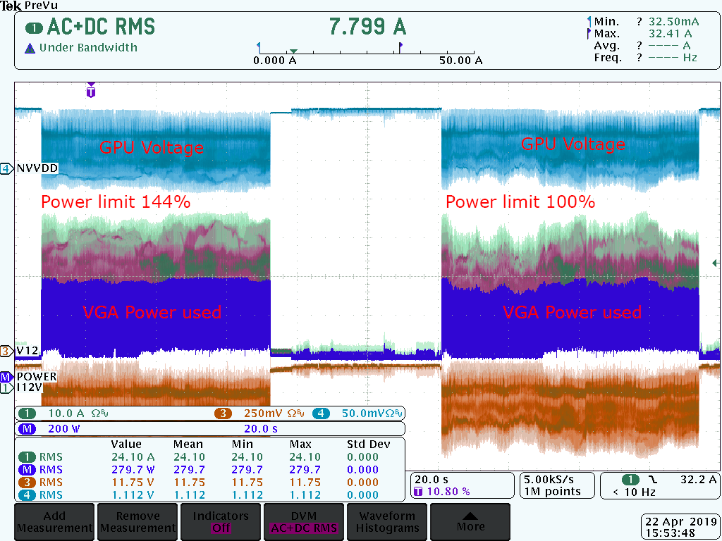
Image 27: Left is power limiter set 520W, right is stock 360W setting
Make sure to max out power limiters to ensure best performance, even when reported power levels looks same.
Now you may ask, how can I get card to show advertised 520W in Precision X1 or OLED? Well, that’s a lot of power and Precision X1 will give you only averaged value. The performance will be capped significantly way before you’d be able to reach averaged 520W power reporting in PX1. Image 28 an example of what power readout looks like when NVVDD voltage is bumped just a little bit, to 1.10 V set.
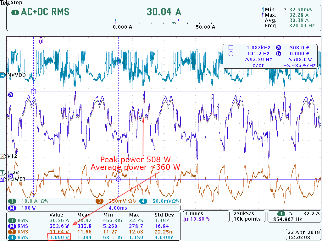
Image 28: Power readout in 3Dmark GT1, with increased NVVDD
Peak power already going to 508W, and increasing voltage any higher will cause a power cap and lost performance, even though average RMS power would be reported just 360W. Ofcourse, if your application/game stressing GPU less than 3Dmark TimeSpy, you would have some more headroom before hitting power cap, but that cannot apply to every benchmark/app.
Loadline setting is yet another setting that have significant impact on stability, temperatures, power and voltage levels available for GPU.
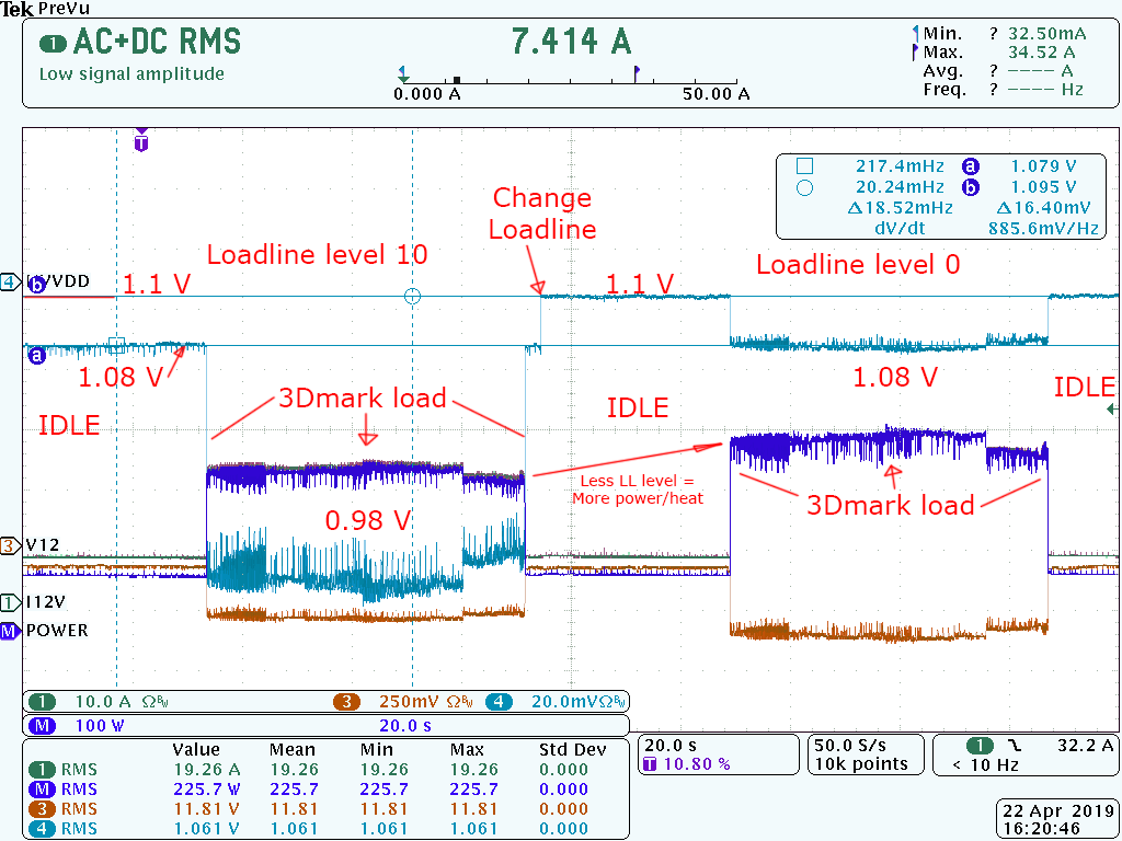
Image 29: Loadline impact on GPU Voltage between Level 10 and Level 0.
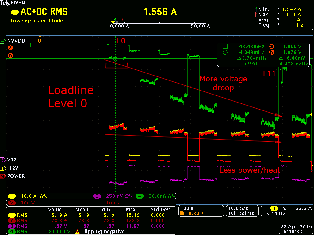
Image 31: Animation on different loadline settings, Level 0, 2, 5, 8, 10, 11 and Auto/L10.
All this is important to understand if you want to maximize the performance of 2080 Ti GPU. This is also the main reason why I suggest to benchmark and test performance of each setting change, instead of just going for maximum frequency possible. Days, when MHz and volts translated into better framerates, are long gone with the introduction of technology like TurboBoost and active power monitoring/limiting circuits.
Few notes on GPU quality
Improved board design, good memory and optimized power alone are not the only things that make KPE special. Actual GPU that goes onto KPE card is not random of the shelf part but selected to meet target performance specifications.
Impact from different OC potential between CPU or GPUs (same model!) is easily visible even on normal cooling. It is well known and typical with many performance enthusiasts to buy multiple units of CPU or graphics card to find better performers for daily use and reselling the “less overclockable” samples on used market. This cost extra time, money and stress. With a limited and expensive card like Kingpin Edition RTX 2080 Ti doing this selection process would become really hard.
So if this pre-selection process to use only fast silicon is done during graphics card manufacturing and QC, then the whole thing is simplified and there is no need to buy multiple cards in hope to find a great overclocker. But testing GPU is a lengthy and tricky process, resulting in limited availability of the cards in small batches. Pre-testing GPU in BGA package is not as simple as just dropping LGA CPU into the motherboard and running 3Dmark.
VRM design overview, available tuning and hardware controls
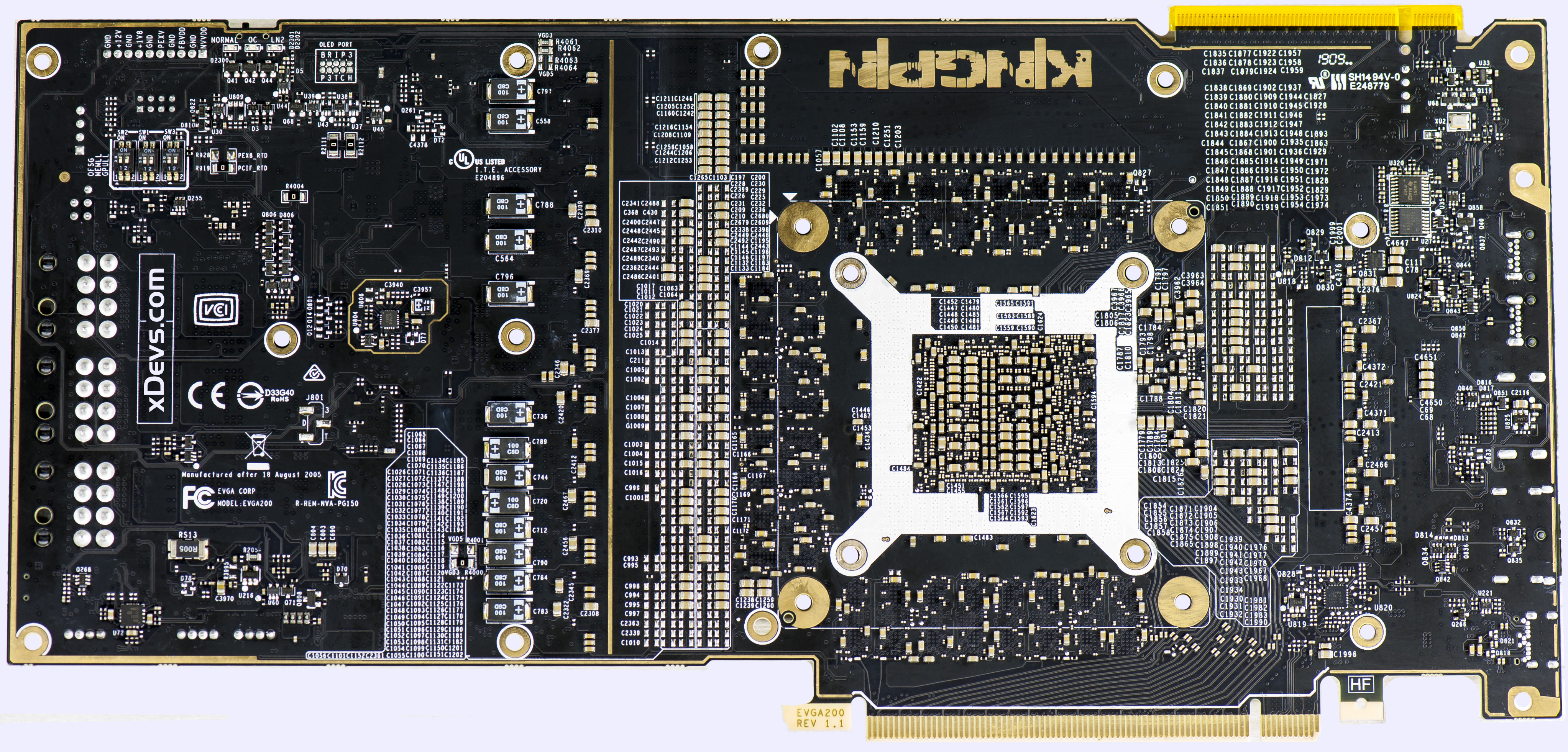
Image 32: Naked EVGA RTX 2080 Ti K|NGP|N Edition card, bottom side
Lot of design effort was spent on high-efficiency digitally controlled voltage regulation solution. VCORE power rail supplied by no less than 16 phases with MPS Smart PowerStages. PowerStage is integrated IC that have high-current MOSFETs, drivers and current balancing/monitoring circuitry. PowerStage we use here is MPS MP86956, driven by MPS2888A controller.
If you was paying attention to our previous guides and materials about graphic cards, then it’s obvious to see very similar VRM used on much more expensive Titan V graphics card. And if VRM was good enough for that much more expensive Volta GPU, running with HBM memory, it’s already good enough for Turing TU102.
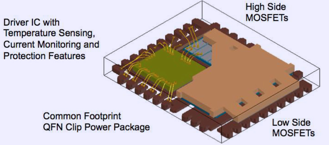
Image 33: Internal design of integrated PowerStage. Courtesy ON Semi website.
Essentially SPS provide everything that you need to make one switching converter, except the master controller and inductor. Each of these PowerStages taking +12V input from ATX power supply and regulate it down to maximum 60 A of current, with output voltage levels up to 1.80 VDC. Typical efficiency running at usual voltage levels around 1.2-1.3 V during extreme overclocking is above 90%, so there is no problem to handle VRM thermals even with just little airflow.
The SPS designs on modern high-performance VRMs like here also can operate at high switching frequency, over 2 MHz. With an integrated approach, the complete switching power stage is optimized for driver and MOSFET dynamic performance, system inductance, and RDSON so there is a less overall loss. Compact 5 × 6 mm footprint also helps to save PCBA space, which is tight on RTX 2080 Ti KPE.
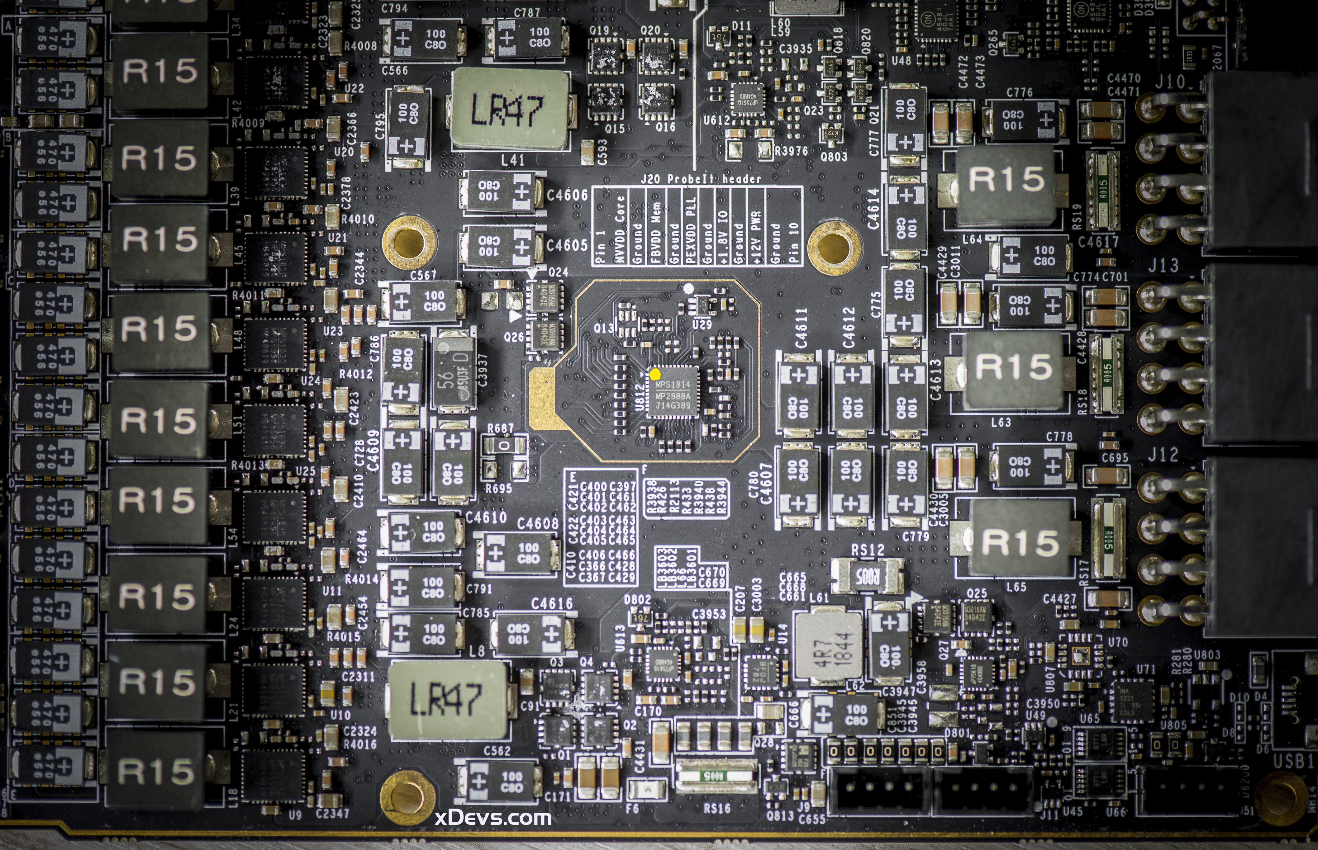
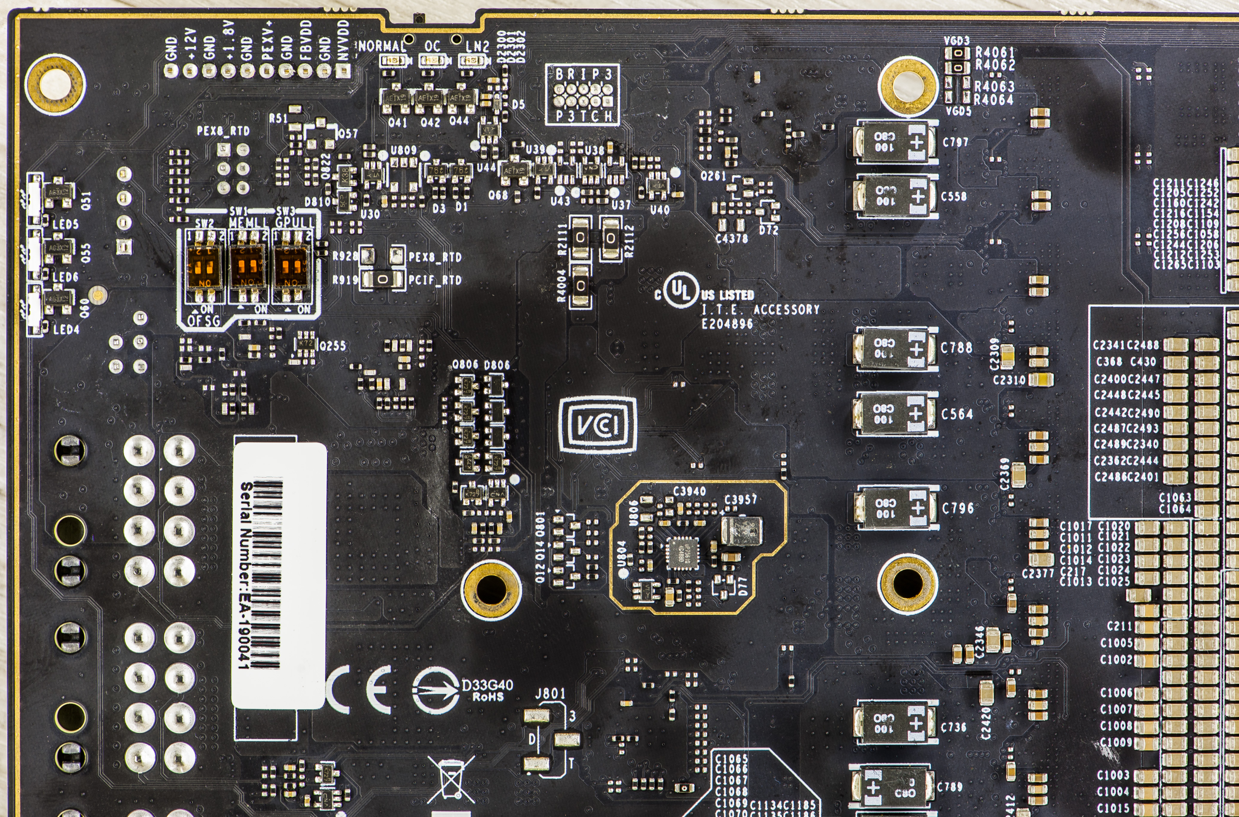
Image 35-36: MPS2888A controller in center-right and auxiliary power parts on the PCBA’s back
To meet fast transient demands such VRM present all input bulk capacitance tank made of low-ESR Panasonic POSCAP and SP-caps types. These capacitors have also less ESL which is important for high-frequency switching VRM. Frequency also adjusted dynamically depends on actual running conditions, which further helps with overall card efficiency.
Also decoupling for GPU package now heavily using ultra-small 0201 size capacitors. 0201 size part measure 0.6 by 0.3 mm, that is only less than 10 times larger than single human hair. And there are hundreds of these behind the RTX 2080 Ti GPU! Reason to use this tiny package is lower parasitic inductance (ESL) of the component pads. Maximum capacitance of smaller package is less, however because of must tighter placement, it’s possible to place more of them and closer to transition via at the PCBA. This allows less parasitic ringing at overshoot at the GPU power balls to provide cleaner power regulation.

Image 37: Decoupling ceramic capacitors on the PCBA bottom side
Using tiny capacitors comes at the cost of higher price for assembly. Not every assembly house can mount hundreds of 0201 capacitors in a small area behind the GPU, and those who do – they will be sure to charge you pretty penny to do it.
ProbeIt monitoring header
For voltage monitoring purposes this card has traditional EVGA ProbeIt, which is a 10-pin 2mm pitch PH-type connector near the top PCB edge. Pin definition as below:
| Number | Description | Nominal voltage level |
|---|---|---|
| Pin 1 | GPU voltage | +0.65 to +1.09 VDC |
| Pin 2 | Ground | 0V ±20 mVDC |
| Pin 3 | MEM voltage | +1.35 to +1.40 VDC |
| Pin 4 | Ground | 0V ±20 mVDC |
| Pin 5 | PLL voltage | +1.00 to +1.1 VDC |
| Pin 6 | Ground | 0V ±20 mVDC |
| Pin 7 | Onboard +1.8V power voltage | +1.76 to +1.83 VDC |
| Pin 8 | Ground | 0V ±20 mVDC |
| Pin 9 | Onboard +12V PCIe power voltage | +11.5 to +12.6 VDC |
| Pin 10 | Ground | 0V ±20 mVDC |
Table 2: ProbeIt measurement port pinout definition
Beware, voltages over the nominal limits are not guaranteed by EVGA or NV. These can be unsafe for everyday use, even on watercooling!
ProbeIt pinout is same since the GTX 680 era, so you still can use your ProbeIt setup if you had it done before. The only difference is replacement of +3.3V probe point with +1.8V rail instead. This I/O voltage is used as main logic level on RTX series graphic cards now, providing power for BIOS, display outputs and various onboard auxiliary logic. Also same helpful label with voltage names is located on the bottom side of PCB near each ProbeIt connector pin to aid connection.

Image 38: EVGA200 KPE BIOS switch and indicator LED location
Nice video review on some hardware aspects and power delivery circuitry is available from Gamers Nexus YouTube channel
Also here are reference points, key resistance values measured with high-accuracy Keysight 3458A DMM on good working card:
| Voltage rail | Resistance measured | Nominal voltage on default |
|---|---|---|
| NVVDD | ~80-110 milliΩ depends on card | 0.65 VDC … 1.06 VDC |
| FBVDD | ~10-20 Ω depends on card | 1.375 VDC fixed |
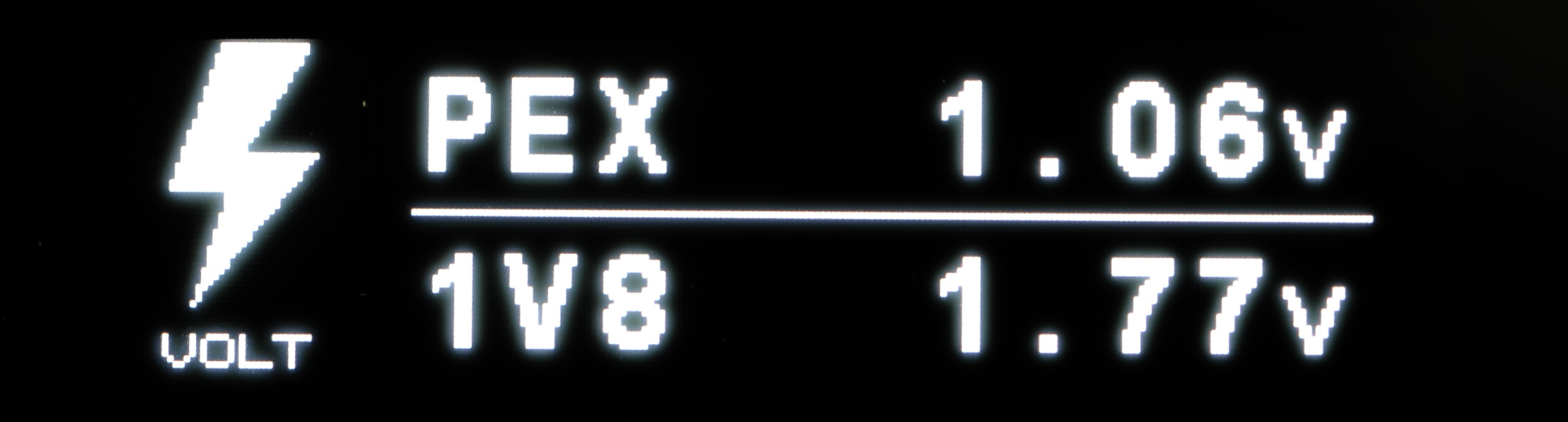
| PEX | ~6-8 Ω depends on card | 1.06 VDC fixed |
| +1.8V | ~380-500 Ω depends on card | 1.80 VDC fixed |
Table 3: Nominal resistance on main power rails on RTX 2080 Ti KPE card
V-Tune onboard switches
There are few hardware switches accessible on the back. These allow some fine-tuning for power controller. These work completely independent from software/BIOS and in real-time. OFSG switch bumps actual delivery to GPU core by two small steps, either +25 mV or +50 mV (with both switches ON). Loadline switches MEMLL and GPULL allow trimming droop that may fit particular benchmark/GPU better, depends on running conditions.
| RTX 2080 Ti KPE | Position | Trim settings switch location |
|---|---|---|
| OFSG – Vcore Offset | Switch 1, +25mV when on | 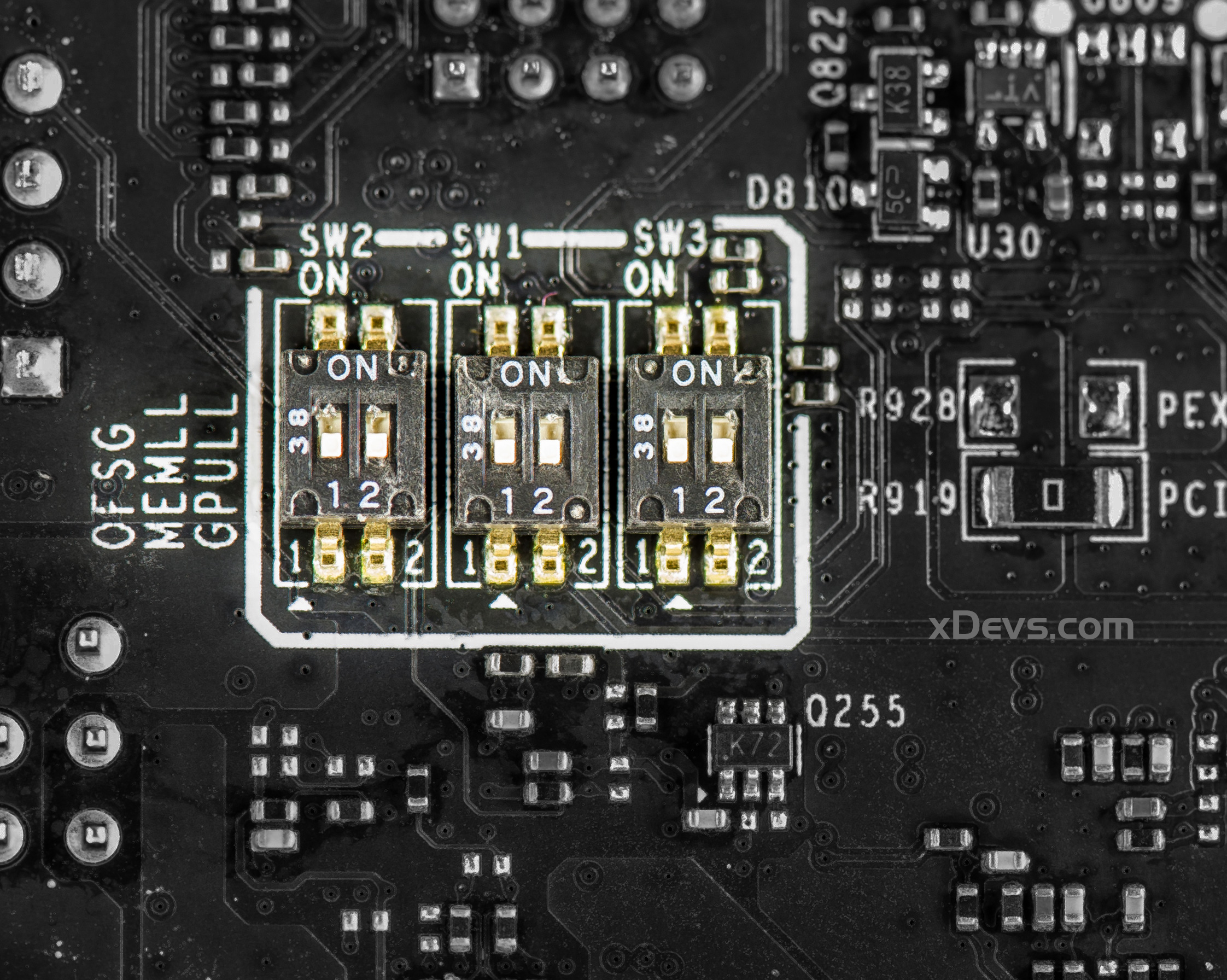 |
| Switch 2, +25mV when on | ||
| MEMLL – Memory Loadline | Switch 1, MEM Loadline Level 1 | |
| Switch 2, MEM Loadline Level 2 | ||
| GPULL – GPU Loadline | Switch 1, FB Loadline Level 1 | |
| Switch 2, FB Loadline Level 2 |
Table 4: Tuning switch definitions and functions
Default settings – all switches positions are OFF.
Normal overclocking with watercooling or even mild chiller setup not expected to have a need in any of these switches. They are rather an additional option for fine-tuning when doing serious extreme overclocking, than a requirement for everyday daily driver OC.
Integrated OLED functionality
To configure OLED mode EVGA Precision X1 software is required. Settings related to OLED available at the dedicated tab, exclusive to Kingpin Edition card.
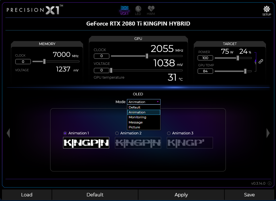
Image 39: EVGA Precision X1 software main UI, in OLED configure mode
KPE is the first EVGA card that gets customized dot-matrix OLED screen. Its main purpose is to display real-time information from various sensors available on the card and aid the owner with debug information when things go wrong. We are used to having debug POST indicator on motherboards to tell us about memory training issues, CPU issues or PCIe device detection problems. So why not to have similar approach on graphics card?
Currently OLED can be used to display many items. Some of the key display configurations shown on table 3.
| RTX 2080 Ti KPE OLED info | Description | PX1 setting source |
|---|---|---|
 |
EVGA Logo | PX1 Fixed image |
 |
Kingpin Logo | PX1 Fixed image |
 |
GPU and memory frequency | PX1 reporting value |
 |
GPU die temperature | Sensor monitor, range -64 °C to +105 °C |
 |
VRM board temperature sensors | PX1 setting, Hardware reporting |
 |
Memory board temperature sensors | PX1 setting, Hardware reporting |
 |
Voltage monitor, GPU and memory | PX1 setting, Hardware reporting |
 |
Voltage monitor, PEXVDD and +1.8V | PX1 setting, Hardware reporting |
 |
Voltage monitor, +5V and +3.3V | PX1 setting, Hardware reporting |
 |
2-line text message | PX1 OLED message |
 |
3-line text message | PX1 OLED message |
 |
3D application frame rate (reported by PX1 OSD) | PX1 and OSD must be running |
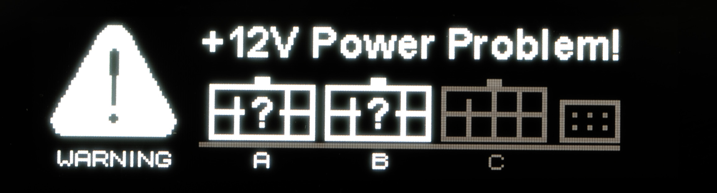 |
Warning for +12V PCIe cable failure | Hardware-only function |
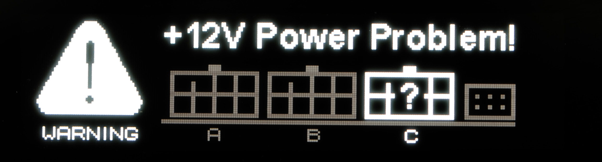 |
Warning for +12V PCIe cable failure | Hardware-only function |
Table 5: OLED display examples and configuration options
PX1 must be running in background to allow readout for GPU and memory frequency (OSD not required for these items). If you want to display framerate – OSD also must be enabled.
Rest of the items, like fan speeds, voltages, temperature monitors are only configured by PX1, after which onboard VGA hardware will refresh readings on OLED, even if you are not in OS/PX1 not running.
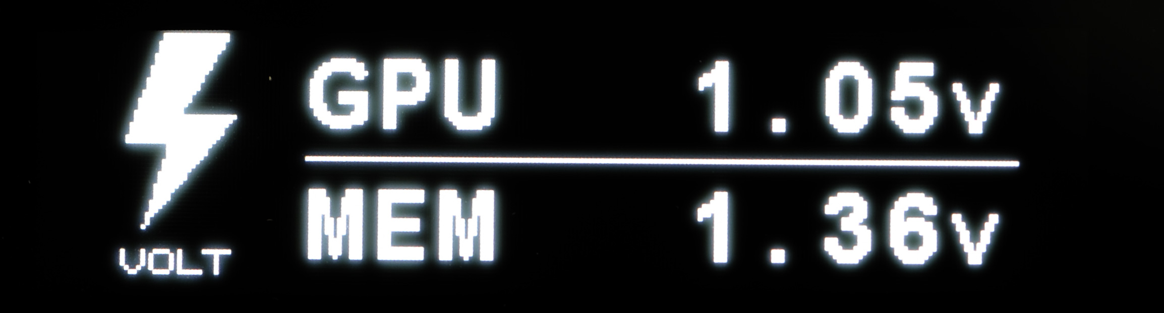
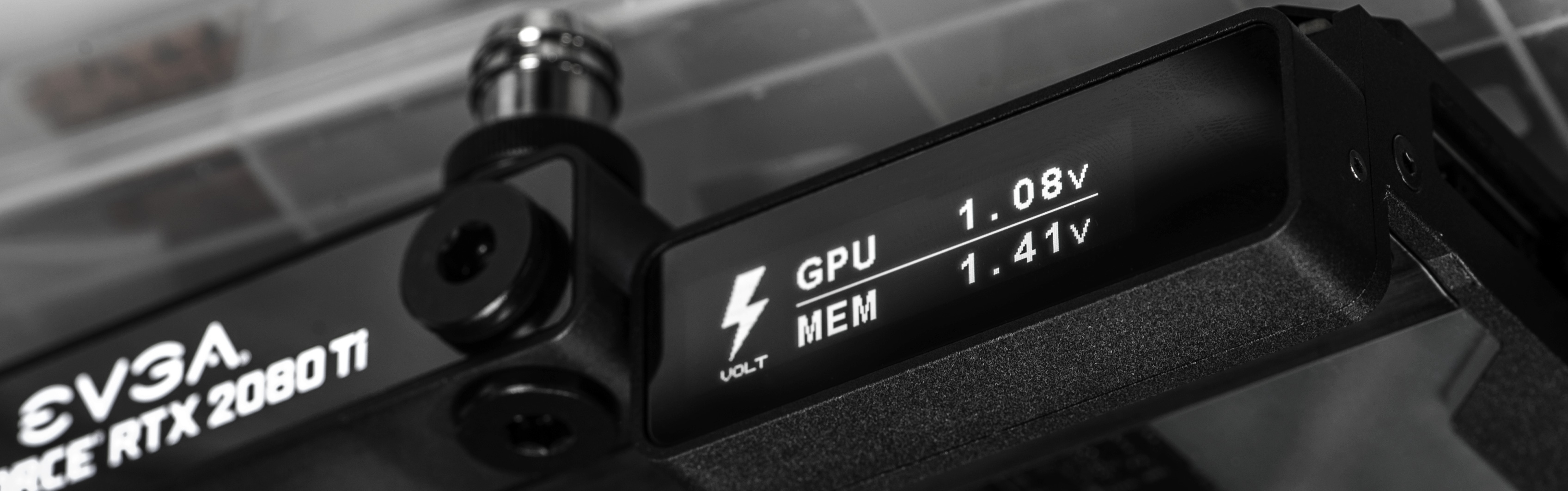
To see real voltage readout on OLED be sure to select GPU NVVDD (for core voltage) and GPU FBVDD (for memory voltage) sensors in monitoring section on PX1. Selecting GPU Voltage sensor will report only driver requested value, not the real hardware measurement.
Extreme OC OLED kit
This card also supports optional LN2 OLED bracket kit which consists of metal frame to mount OLED and electronics to bare PCBA. It’s available at EVGA online store as accessory.
With this kit, you can use OLED functionality, even with 3rd party aftermarket cooler, including LN2 extreme cooling containers, like Kingpincooling.com ICON 3.0.
This section guides you thru the installation of such kit in steps. It’s a bit of a treasure hunt.
STEP 1. Remove backplate and Hybrid AIO metal shroud
First, we need to remove the backplate and unmount the metal cover to gain access for OLED assembly.
Because OLED glass is not included with bracket kit, you will have to take existing OLED from a stock Hybrid cooler.

Image 40: 18 backplate mount screws that need removal
Undo 18 Philips-head screws that hold the card together. Screws marked with yellow circles hold the front metal cover to the card. Easier to remove them first, and remove a cover. Red screws hold heatsinks and parts mounted to PCBA. With shroud removed, put card on the soft surface and remove red screws to free the backplate. Backplate and OLED bracket kit cannot be installed together without interference at mounts.
Now that backplate is removed, put screws marked red back to fix heatsinks back onto PCBA.
STEP 2. Remove OLED from the Hybrid AIO shroud
Unlatch FPC connector that have attached cable from OLED glass. Carefully lift gray latch up with dull flat tool or fingernail on the connector. Release cable by gently pulling it out. Now carefully pry plastic mylar that covers OLED and removes it. Be careful not to put physical force onto OLED glass, it is thin and easy to damage.
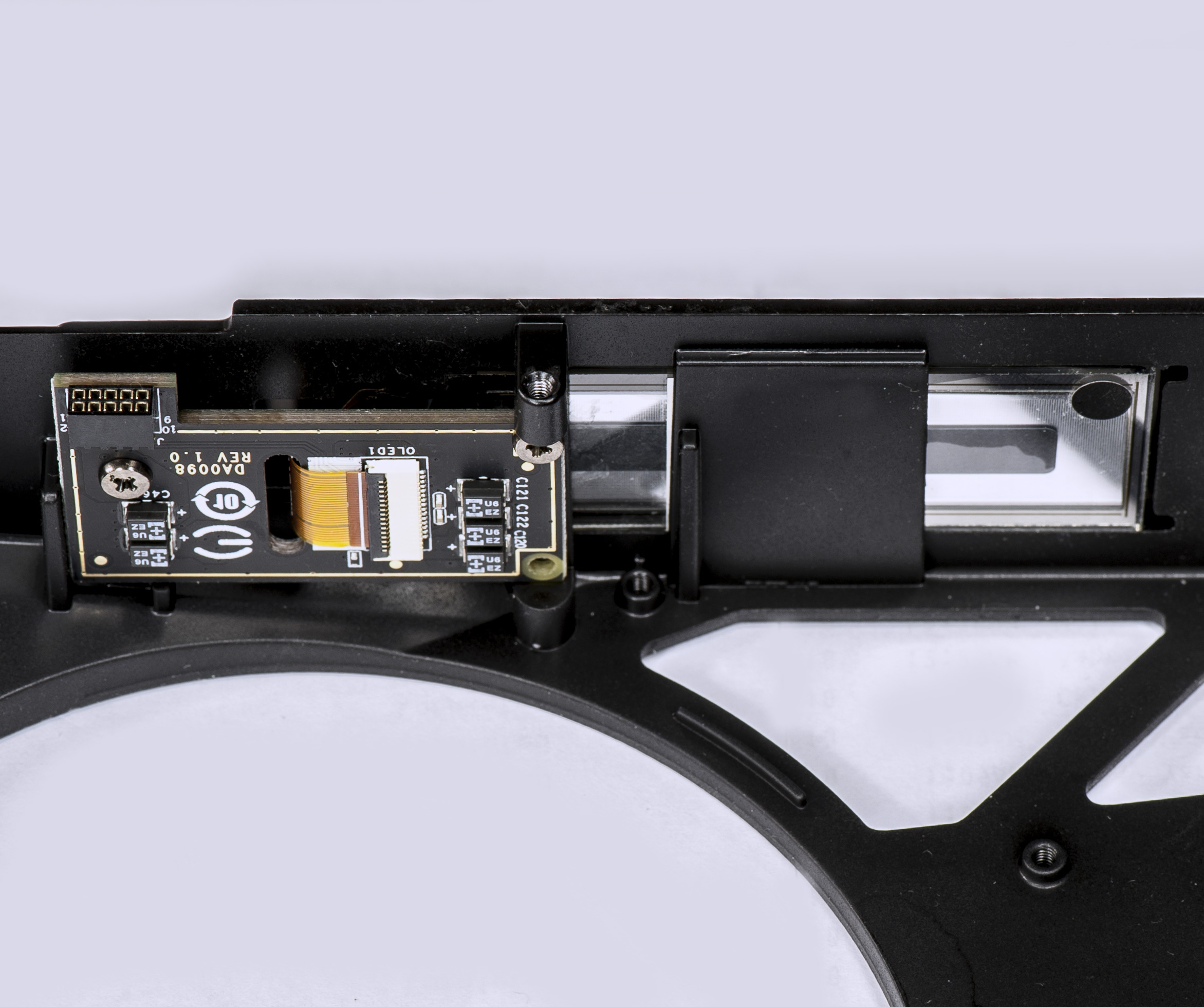

Image 41-42: Removing OLED glass from the metal cover shroud
Remove OLED from the cover and store it nearby. We are done with the cover here.
STEP 3. Prepare kit for installation
Kit includes the next components:
- Black anodized aluminum frame
- 2 longer screws to attach frame to PCBA
- 4 short screws to mount EVGA DA0099 interface board onto the frame
- Spare mylar with an adhesive layer
- 8-pin interface interconnect cable
You will need just a small Philips-head screwdriver to perform the installation.

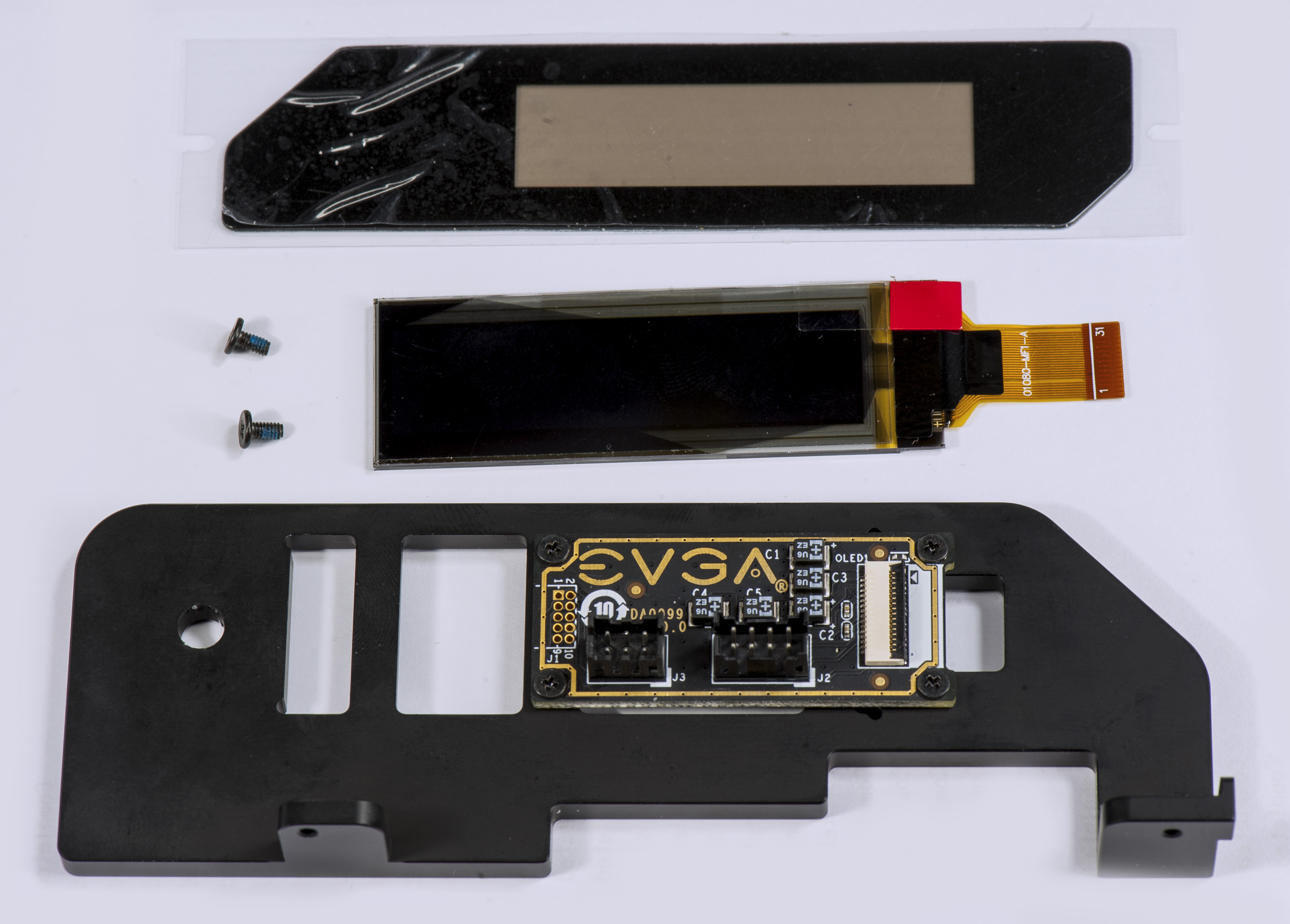
Image 43-44: LN2 bracket kit with ready to install OLED glass
Install board onto frame and mount it using 4 short screws.
Avoid using longer screws when mounting interface PCBA to prevent OLED glass damage.
STEP 4. Place OLED glass on the frame. Ensure it fits firmly and flush to the surface.
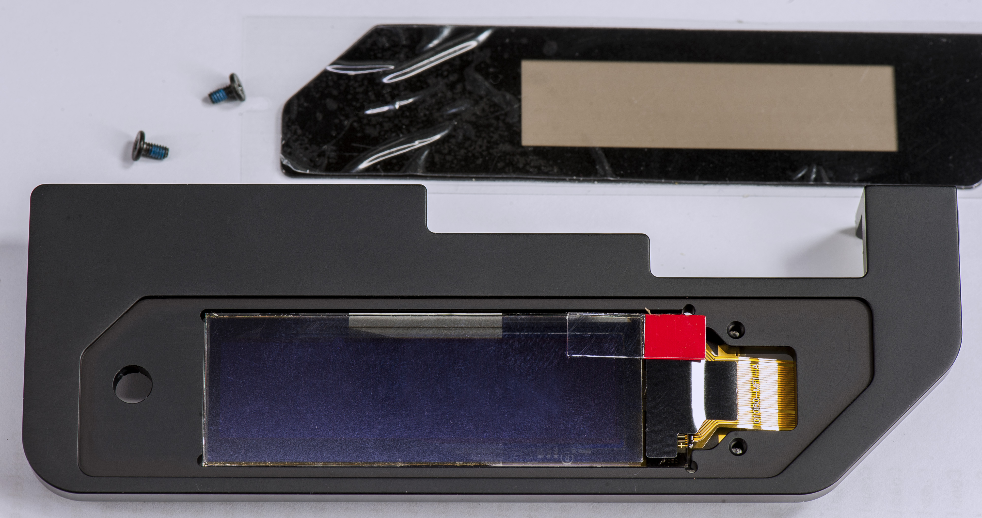
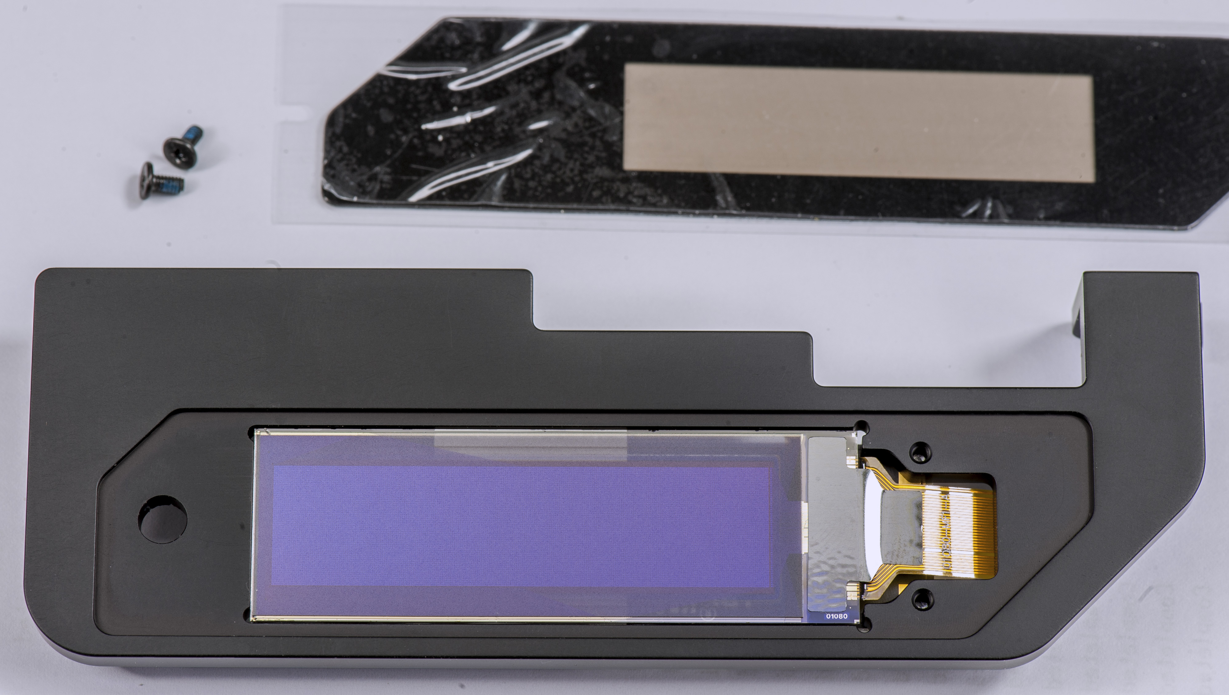
Image 45-46: OLED glass placed in the metal frame
Place OLED on frame. Make sure OLED surface is clean and dust-free.
Install protection mylar, following correct orientation. Press gently on corners for good adhesion to the frame.
STEP 5. Connect OLED flex connector to the interface board
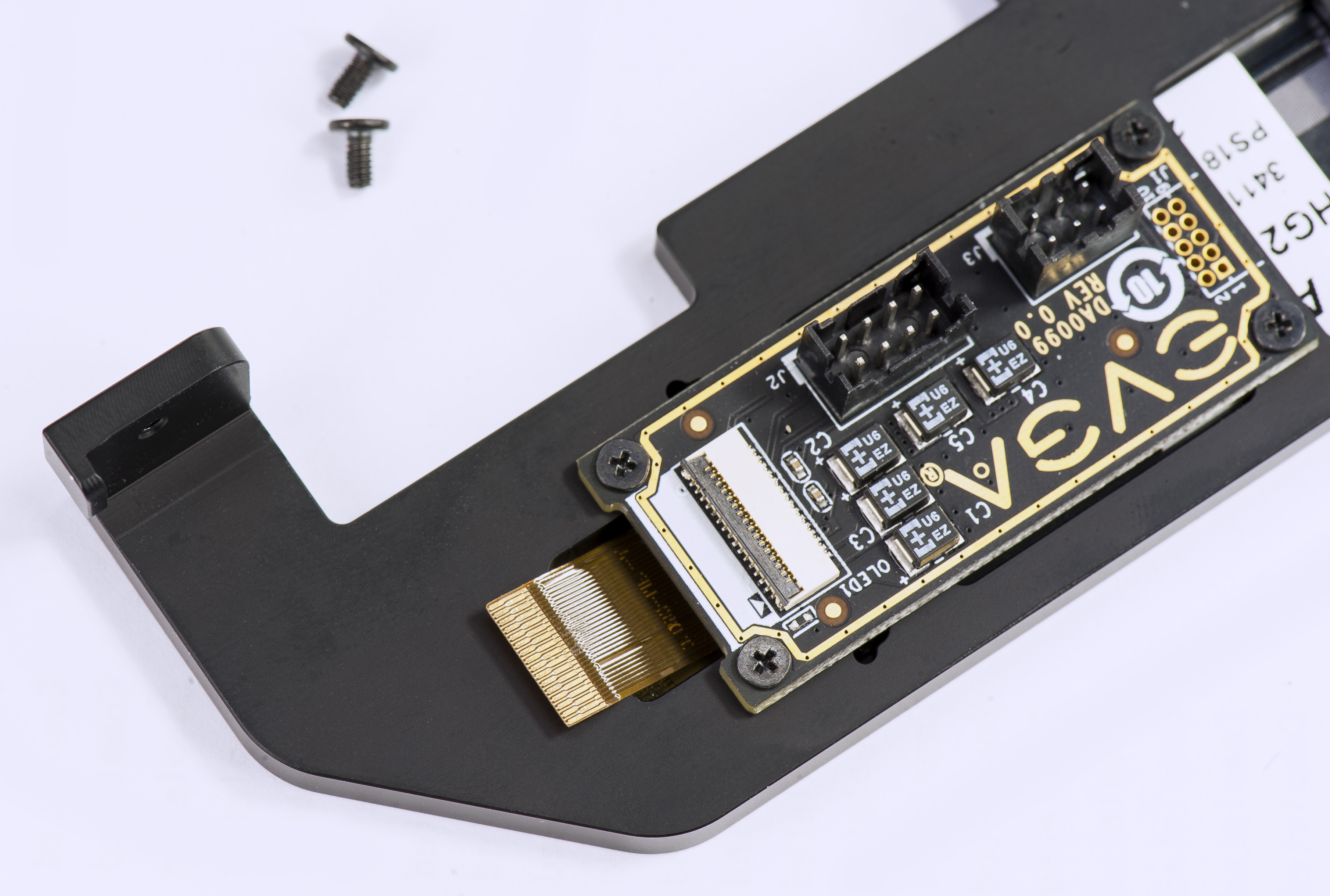
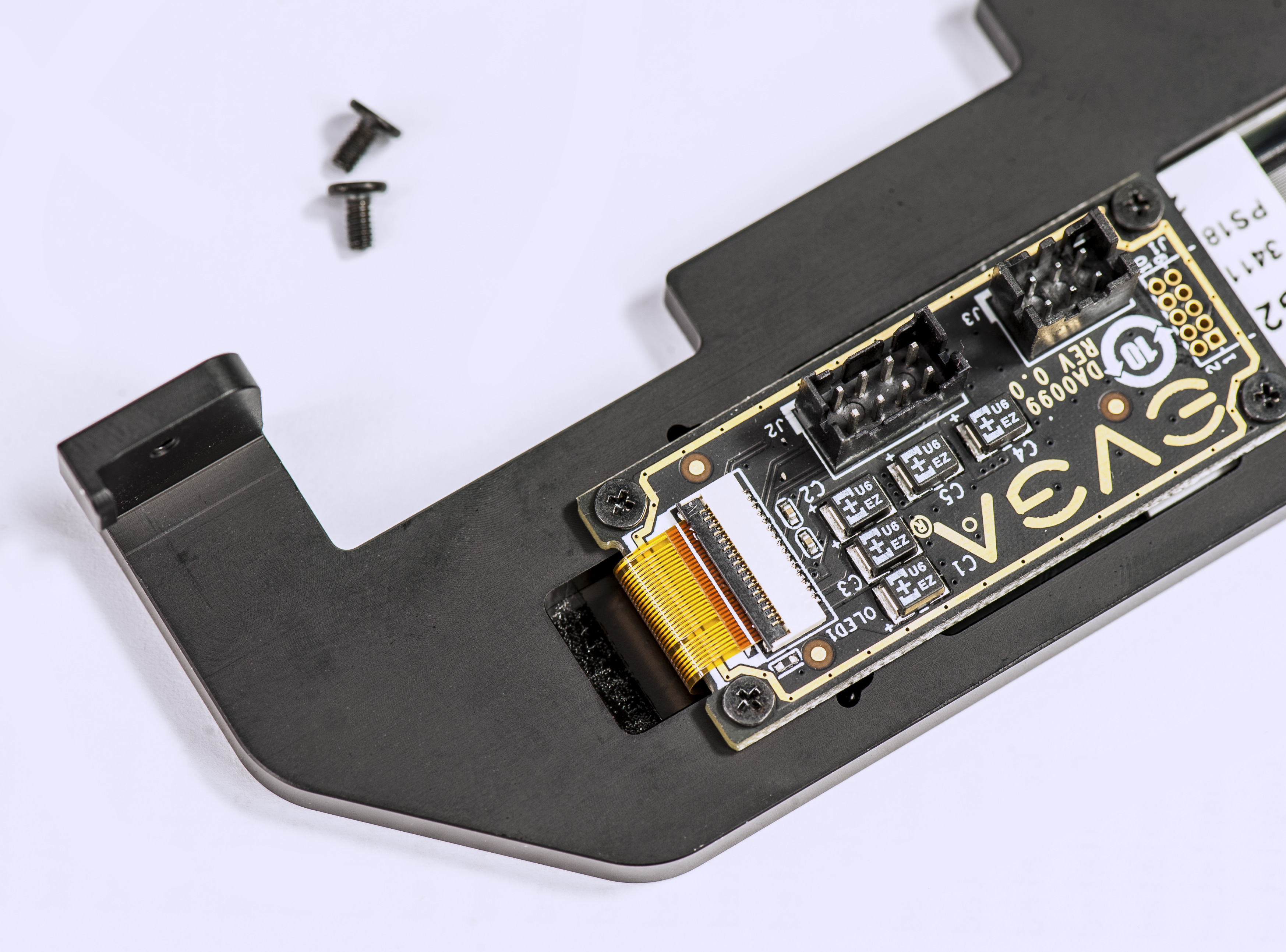
Image 47-48: Connecting FPC cable from OLED to interface board
Unlatch the connector by a gentle lift of the gray lever straight up.
STEP 6. Connect PCBA interface cable to VGA card
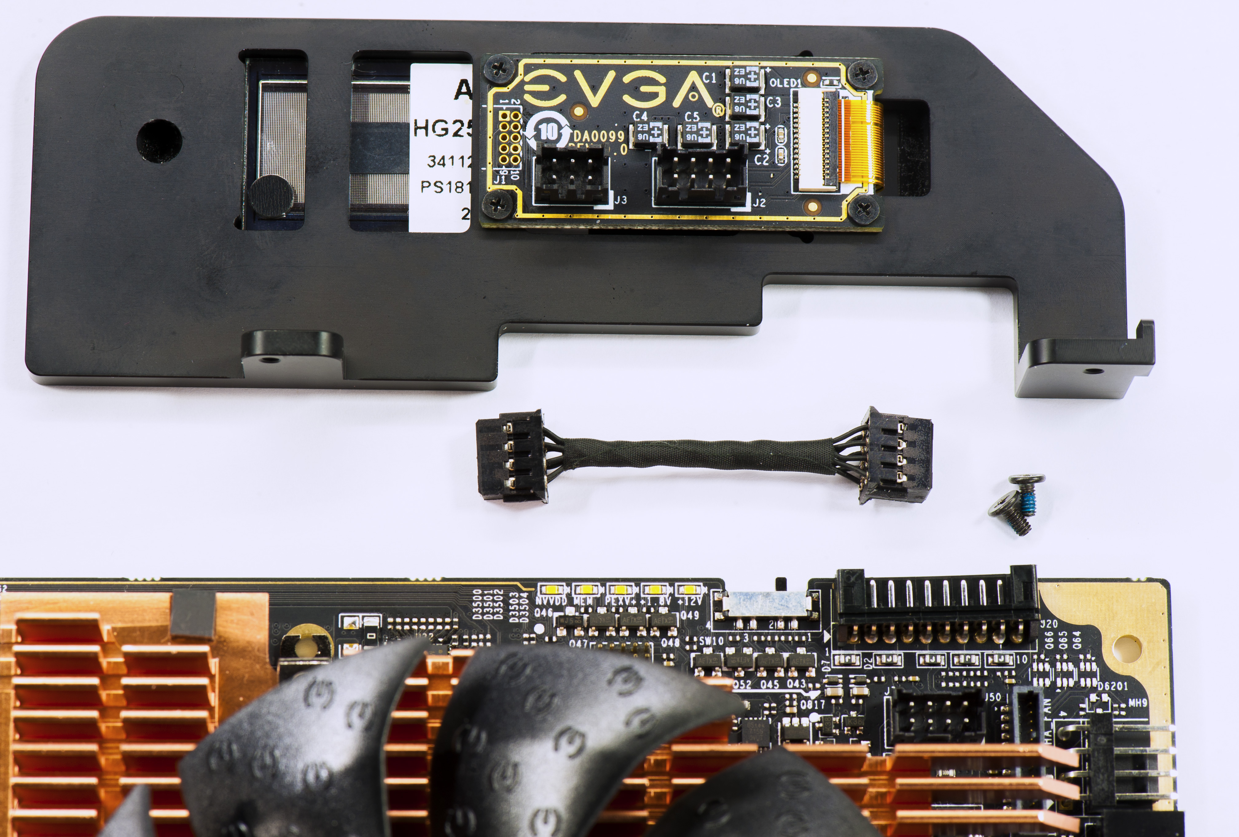
Image 49-50: Connection of the OLED kit frame to RTX 2080 Ti KINGPIN, using 8-pin cable
Plug keyed 8-pin cable into both interface board and VGA card. Connector should plug normally, without use of excessive force. There are plastic notches to prevent installation in wrong orientation.
STEP 7. Mount complete assembly
Image 51: Connected and assembled kit in place
Use two longer screws to attach assembled frame to card.
STEP 8. Check everything and power on
Make sure all connectors aligned correctly and locked firmly.

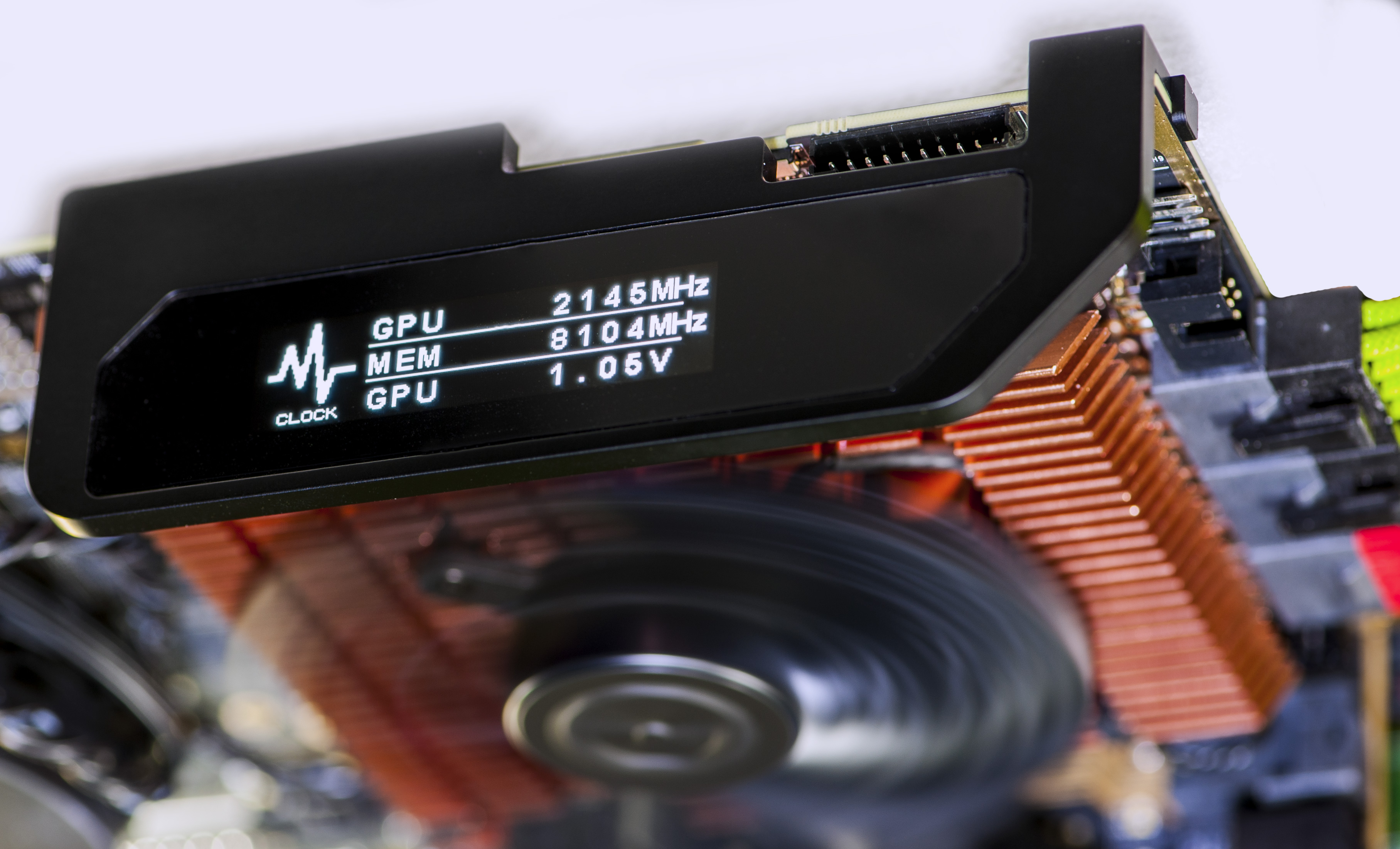
Image 52-53: OLED kit is ready to go
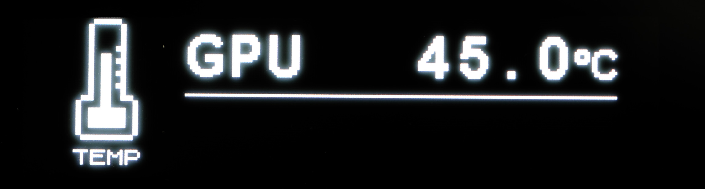
Now boot the system with card installed and configure OLED thru EVGA Precision X1 software. For LN2 benching showing GPU temperature and GPU Die temperature sensors is most useful to monitor thermal interface quality and grease contact. GPU Die readout can read negative temperatures, down to -64 °C.
Real voltage software monitoring
As you already know, regular hardware health monitoring software is usually unable to show real voltages supplied to the GPU and also disregard additional voltages like memory and PLL power. This is due to the fact that the NVIDIA driver only supports readout of “requested” voltages, or GPU VID setting. It does not have a standard mechanism to report real voltages presented from VRM. Most end users are not aware of this detail and expect to see real voltages. That’s why we often see many confused people in forums/discussions who see LN2 records with 2500 MHz+, but are often confused about reported clock/voltage measurements and left scratching their heads wondering how is such a high clock possible with only 1.093V?
Precision X1 and Kingpin Edition RTX 2080 Ti will report real monitoring, just like standalone DMM connected to ProbeIt. Now with onboard OLED display, there is no need for separate DMM when running benchmark sessions. To further comply with this, EVGA will sell optional “Extreme OC pack” with metal frame to support OLED display and it’s interconnect board on main graphics card PCB, while allowing full removal of Hybrid cover and watercooling solution to allow LN2 pot setup.
BIOS & Tools
BIOSes in this section are compatible only with EVGA RTX 2080 Ti KINGPIN card and will not work and may damage any regular 2080 Ti FTW3/SC or any other brand RTX card.
Just like all previous KINGPIN Edition cards, 2080 Ti KPE has three independent different BIOS ROMs and the corresponding switch to select between them. Default configuration with switch locked at right (towards power plugs), setting on NORMAL BIOS position. BIOS difference comparison between the three is presented in table 4.
| Normal BIOS switch | OC BIOS switch | LN2 BIOS switch | |
|---|---|---|---|
| BIOS mode LED indicator | Green | Orange | Red |
| GPU Clocks Boost/Memory clock | 1.8 GHz / 14 Gbps | Same as Normal | Same as Normal |
| BIOS Version | 90.02.30.00.77 | 90.02.30.00.78 | 90.02.30.00.79 |
| 240mm Hybrid Fan speed range | 0% – 48% | 12% – 55% | 20% – 100% |
| VRM Fan speed range | 20% – 53% | 20% – 84% | 41% – 100% |
| Fan stop at idle/low load | Yes | No | No |
| Total Power Limit | 360W | 360W | 360W |
| Max TGP Limit | 144% | 144% | 144% |
| Protection function | Full protection | Full protection | No temperature protection |
Table 6: BIOS ROMs and settings on the card
LN2 BIOS switch position disable temperature protection by hardware. This is a crucial feature to enable for LN2-type cooling, but totally unnecessary(and even dangerous) for watercooling/aircooling use. Using LN2 BIOS position is not recommended for daily use, but available for benchmarking purposes.
If you want to enjoy maximum fan speeds that 90.02.30.00.79 version provide, you can flash it into “Normal” or “OC” position instead, to maintain thermal protection mechanisms and safety. Any of the three BIOSes can be flashed with unofficial KPE BIOS ROMs and operated independently.
BIOS can be flashed using NVFlash from TechPowerUp. You need version 5.513.0 or newer.
Card is already shipped with three different BIOSes, available for download as backup dumps:
Normal BIOS (Green LED), Version 90.02.30.00.77 This BIOS is stock baseline, +144% Power target limit
OC BIOS (Orange LED, Version 90.02.30.00.78 This one is similar to Normal, but more aggressive fan profile, +144% Power target limit
LN2 BIOS (Red LED), Version 90.02.30.00.79 Unlimited fan speeds, 144% power target, HW set to disable thermal protection for LN2 overclocking.
Custom unofficial XOC BIOS
Current normal BIOS provided above (as shipped with card) with maxed out 144% power limit target already allow GPU to reach maximum everyday frequency without need of special VBIOS or risks involved flashing it.
However, if you want to do benchmarking with extreme cooling, you might want to get purpose built custom ROM from link below. Keep in mind, this BIOS is not for everyday use.
XOC unofficial BIOS, Version 90.02.17.40.88 XOC overclocking version for RTX 2080 Ti KINGPIN card.
This archive is password protected to ensure you have read this guide carefully and agree with the risks involved of flashing custom binary into your KINGPIN. Password from the archive is ipromisenottoRMAthiscard.
XOC BIOS have next limitations to restrict its use only for benchmarking purposes:
- All fans are 100% speed (“jet engine mode”). Fan speed curves or adjustment in PX1 is disabled.
- Temp target is removed.
- Power limit is not there anymore.
- Card ID is generic in this BIOS (meaning you need to use nvflash with -6 parameter to flash into this BIOS or restore original BIOS).
BIOSes in this section are compatible only with EVGA RTX 2080 Ti KINGPIN card and will not work and may damage any regular 2080 Ti FTW3/SC or any other brand RTX card. These BIOS are unofficial and provided AS IS, without any warranty for education purpose only. Do NOT hotlink this BIOS on forums or social media.
EVGA Precision X1 software
RTX 2080 Ti KPE supported by Precision X1 since version 0.3.14 BETA. We always recommend using the latest version.
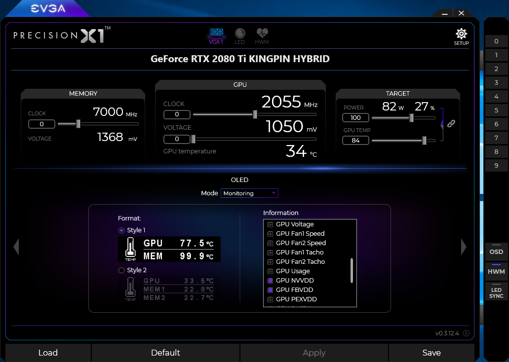
Image 54: EVGA Precision X1 software main UI, in OLED configure mode
KINGPIN RTX 2080 Ti have special hardware to actually measure all the relevant voltages in real-time and report those measurements to Precision X1 which can read and display real measured voltages in software and on OLED. It works automatically with every 2080 Ti KINGPIN graphics card and does not need any settings adjustment. Just make sure you use Precision X1 version 0.3.14 or newer.
EVGA Precision X1 0.4.8.0 47.2 MB
EVGA Precision X1 0.4.4.0 47.2 MB
EVGA Precision X1 0.3.19.0 46.7 MB
EVGA Precision X1 0.3.17.0 BETA, 46.5 MB
EVGA Precision X1 0.3.16.0 BETA, 46.3 MB
EVGA Precision X1 0.3.15.0 BETA, 46.3 MB
EVGA Precision X1 0.3.14.0 BETA, 46.3 MB
There is no limit on reading so even 1.30 V will be reported correctly. Again, this works only for the EVGA RTX 2080 Ti KPE card. Other graphics adapters like FTW, SC-series, or any other 3rd party card would not show additional voltages due to lack of special KPE hardware.
To select real core and memory voltages on OLED, please use GPU NVVDD and GPU FBVDD sensors in OLED settings panel. If you select “GPU Voltage” item, OLED will show driver request voltage, which does represent actual hardware voltage (which may be different, if altered by other tools).
Starting from version 0.3.17.0 Precision X1 will not be doing firmware update checks for KPE card, so to make sure OLED, fan control and monitoring operating correctly, make sure to verify you are running latest MCU firmware on the card. The latest version is E200_FA41 from June 17, 2019. The firmware version can be verified by clicking 🛈 icon next to PX1 version in the bottom right corner.
Binary image and flash tool available here:
EVGA RTX 2080 Ti KPE Firmware, Version FA3F
Older versions for legacy purposes:
EVGA RTX 2080 Ti KPE Firmware, Version FA3E
EVGA RTX 2080 Ti KPE Firmware, Version FA3D
Software way to tweak settings for benchmarking
There is secret Classified tool available to play with various onboard KINGPIN RTX settings for maximum performance tweaking.
Uncheck “Auto” checkbox to unleash the beast. Keep an eye on temperatures! Power consumption and stress to GPU is increased exponentially from elevated voltage, instead of linear for clock frequency OC only.
Do NOT set anything over 1200 mV for any type of near ambient cooling. Even with chilled watercooling and antifreeze your GPU temperatures under load will be positive and giving more juice to poor chip will only throttle it. It’s easy to see by lack of performance scaling (such as 3Dmark score / game fps).
When you use a tool, it’s a good idea not to mess with voltage control in Precision X1. Using multiple programs to control card settings can easily corrupt driver settings and create havoc. Great example of “Too many cooks in the kitchen”, because different applications do not communicate to each other, to gracefully apply settings.
This tool applies settings to hardware directly and settings will stay until the card is power cycled (complete shutdown). If you need reset to default settings – just power cycle the system, that will clear any classified settings. You do NOT need to keep tool open to maintain settings, they will stay set, until the card is power cycled.
For LN2 benchmarking make sure to disable NVVDD OCP and enable LN2 VRM mode settings!
EVBOT way to tweak real-time settings
Firmware for EVBOT is available here, version 69. This version can be updated to EVBOT thru any EVGA KPE card, equipped with EVBOT connector. Classified tool functionality also available thru elusive EVGA EVBOT controller, for the chosen ones than still have it.
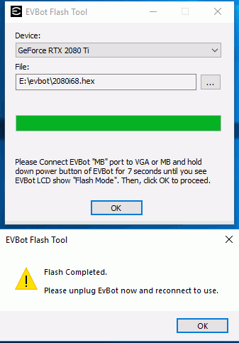
Image 55: EVBOT flashing tool, showing update process with text i68 firmware
Firmware update tool is bundled in ZIP-archive together with firmware.
- Copy tool to a folder on HDD.
- Connect EVBOT cable to KPE VGA card. Another end connects to EVBOT’s MB port.
- Press and hold top POWER button for 5 seconds
- EVBOT should go into FLASH MODE and LCD backlight should be OFF
- Run flash tool software, point it to correct 2080i69.hex hex-file with firmware and press OK
- After update, which normally takes a minute you will be prompted to disconnect/reconnect EVBOT.

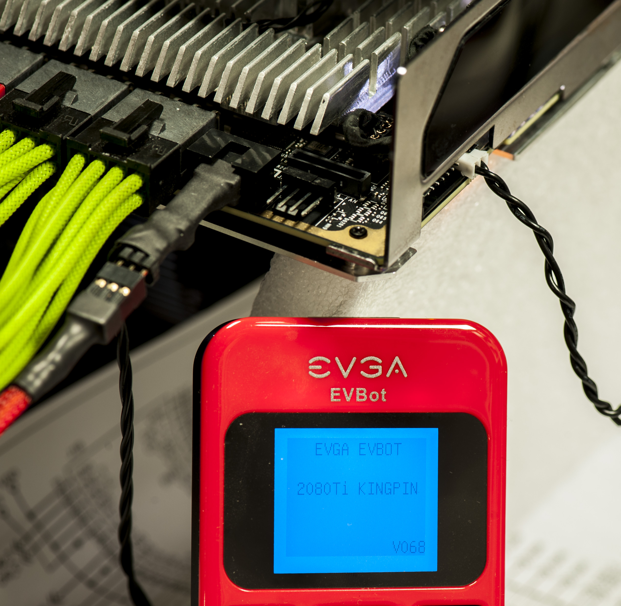
Image 56-57: EVBOT in flash mode at the left, updated RTX KPE EVBOT on the right
This firmware version does not support any older KPE VGA. If you need to flash back older firmware, you can use the same card/tool.
Water-cooling compatibility
HydroCopper full-cover block for this card is also available.
To maintain assembly OLED functionality for aftermarket coolers EVGA will sell support bracket kit, that will allow to mount OLED glass and interface board onto PCBA, while having Hybrid cover removed. HydroCopper block will come with own OLED assembly preinstalled, due to risk of damage for thin fragile glass screen if disassembled.
Hydrocopper block option
Sadly this time around KPE does not have SKU with preinstalled HydroCopper full-cover waterblock to obtain best performance possible for daily use. However, block is available separately for DIY installation by user.

Thermal pads are already preinstalled on the block, just peel off protection film before installation. If any of the thermal pad damaged and need replacement, you can use size listed below as a reference:
- Memory pad, 3 pcs : 55 × 15 × 1.25mm thickness
- Right (near I/O) VRM pads : 50.5 × 6.3 × 1.5 mm and 54.5 × 15 × 1.5 mm
- Left VRM pads : 25 × 15 × 1.5 mm, 90 × 15 × 1.5 mm and 114.5 × 6.3 × 1.5 mm
- Little square for FETs, 2 pcs : 10 × 10 × 1.5mm
HC Block allows fitting installation with standard G1/4” BSP ports. Ports with caps are located on all three orientation sides to allow user loop customization.

Due to fragile nature of thin glass-covered OLED screen, it comes already preinstalled and ready to use in HydroCopper unit. Single cable need to be plugged into RTX KPE mainboard for OLED and white nameplate logo backlight operation.
OLED is identical to the one used with Hybrid cooler, it have same controls, functionality and looks.
Nameplate logo is backlit on the fitting port is backlit by white only LED. LED brightness can be adjusted or completely turned off via Precision X1 version 0.4.4 or newer, with E200 firmware version 41h or newer.
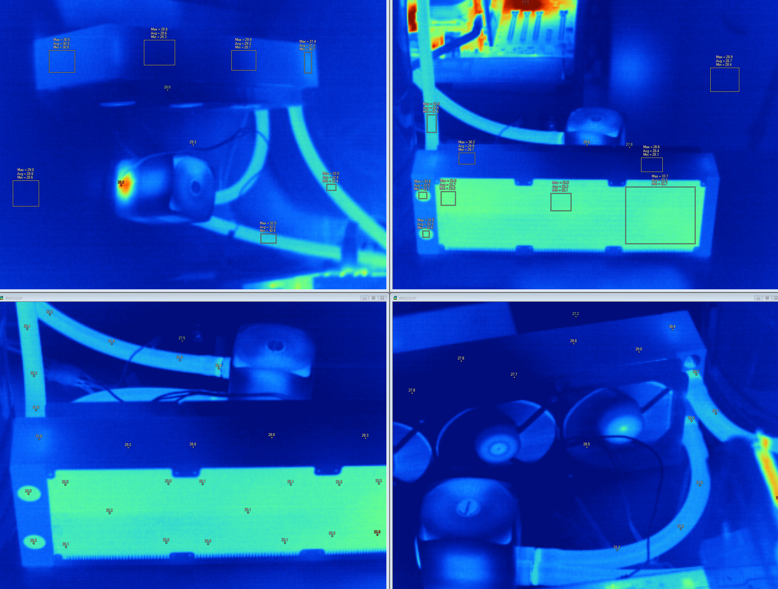
Hydrocooper block temperature in 3Dmark TSX Stress test
3Dmark Time Spy Extreme Stress test suite run temperatures and states recorded below for reference. Card is running stock Normal BIOS, with power/temp limit maxed out by Precision X1. No overclocking applied, all VRM settings are at default. Ambient temperature is +25 °C.
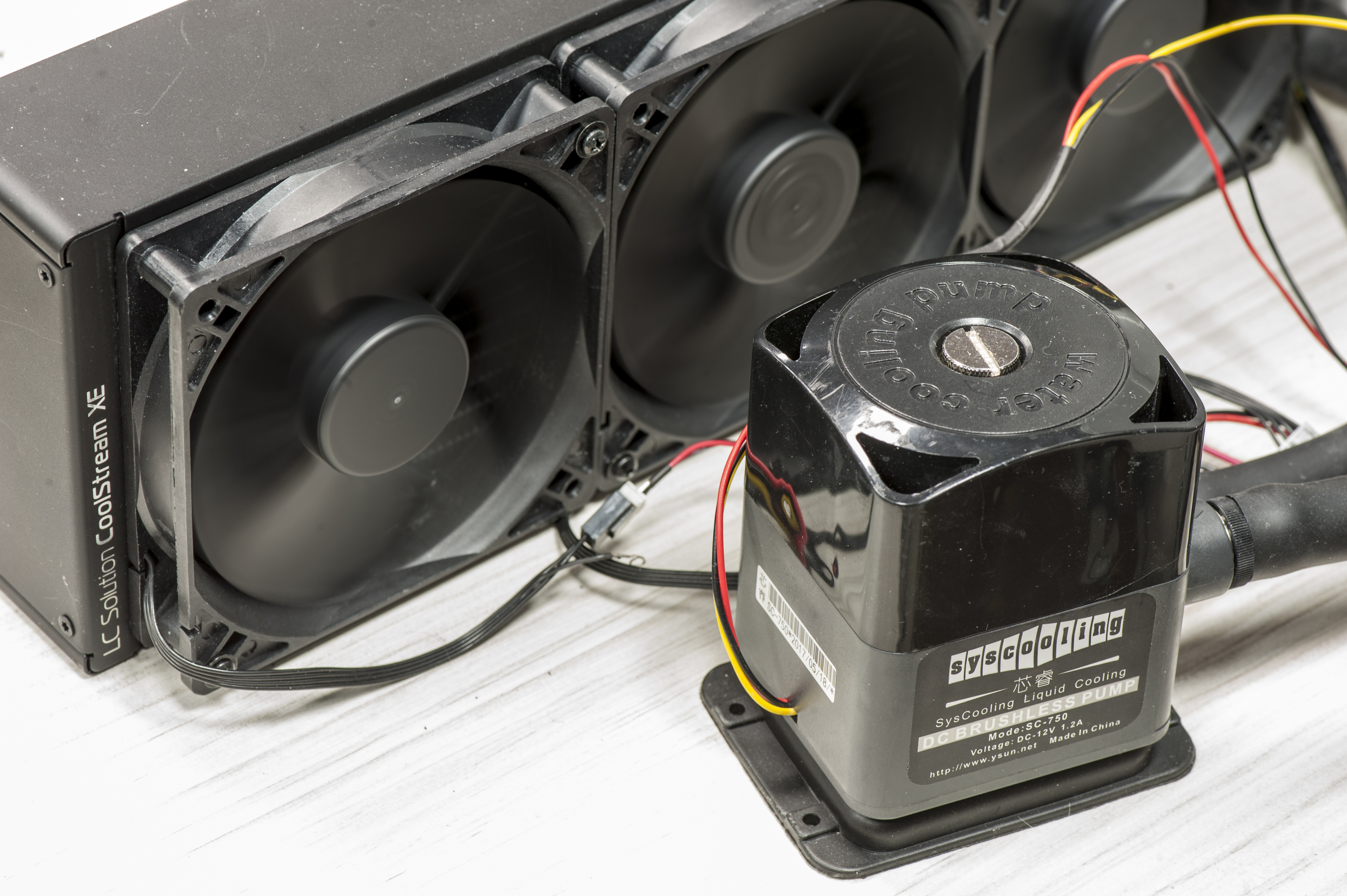
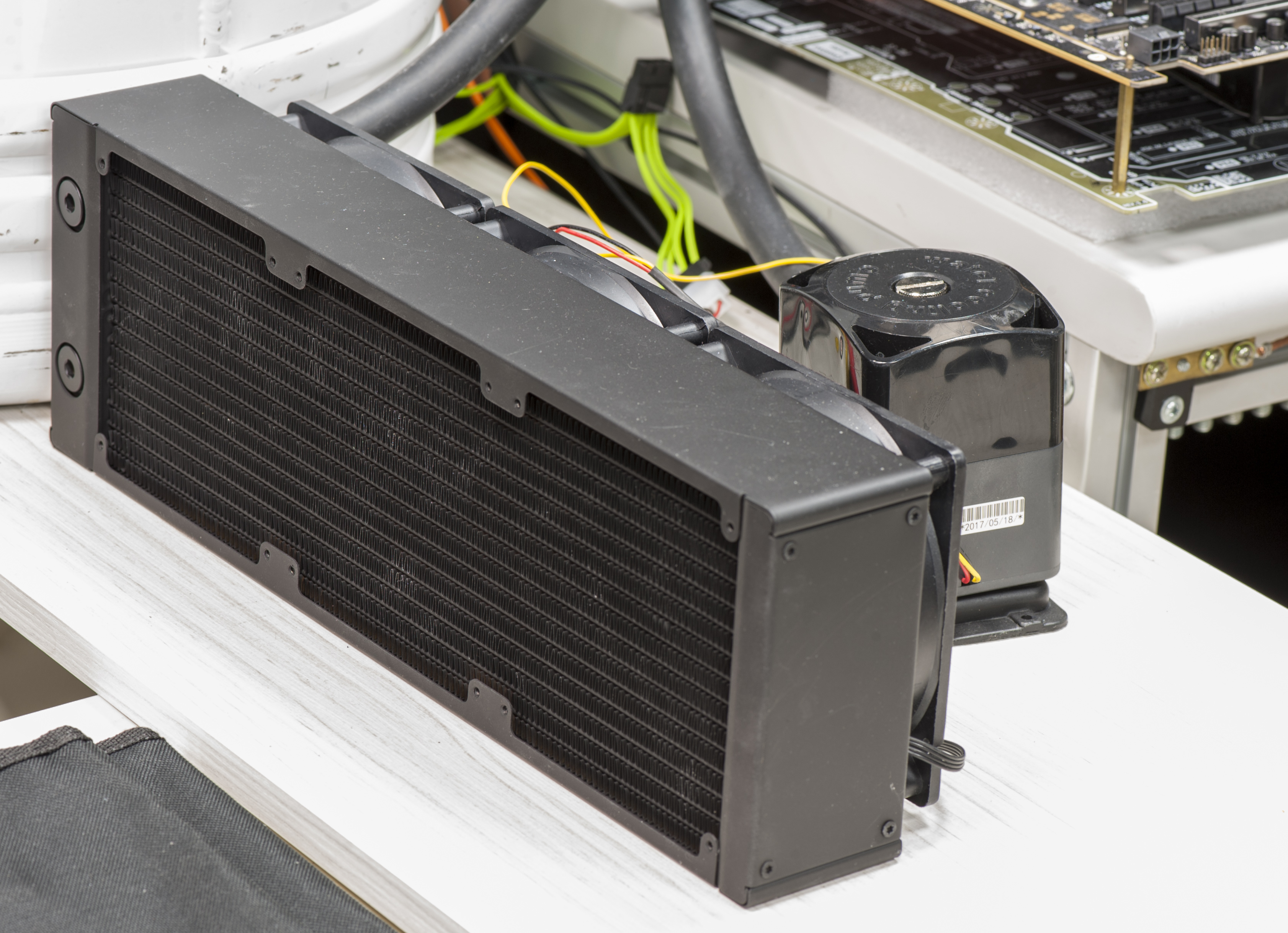
The system used for test: EVGA X299 DARK motherboard with 7980XE CPU, 2×4GB DDR4 RAM, production EVGA 2080Ti RTX KPE with production HC block, EVGA NEX 1500W PSU.
CPU was cooled by own EVGA CLC 240 AIO, with no airflow around motherboard (VRM heatsink on motherboard not installed). GPU is the sole device on the watercooling loop, which has the next components:
- EK CoolStream XE 360 radiator with 3 × 120mm normal speed fans from 2080Ti RTX AIO radiator
- EK-Tube ZMT Matte Black 19,4/12,5mm tubing
- Syscooling SC-750 pump (750 liters/hour spec, +12VDC powered)
- EK-HFB Fitting 13mm for pump, radiator, HC block
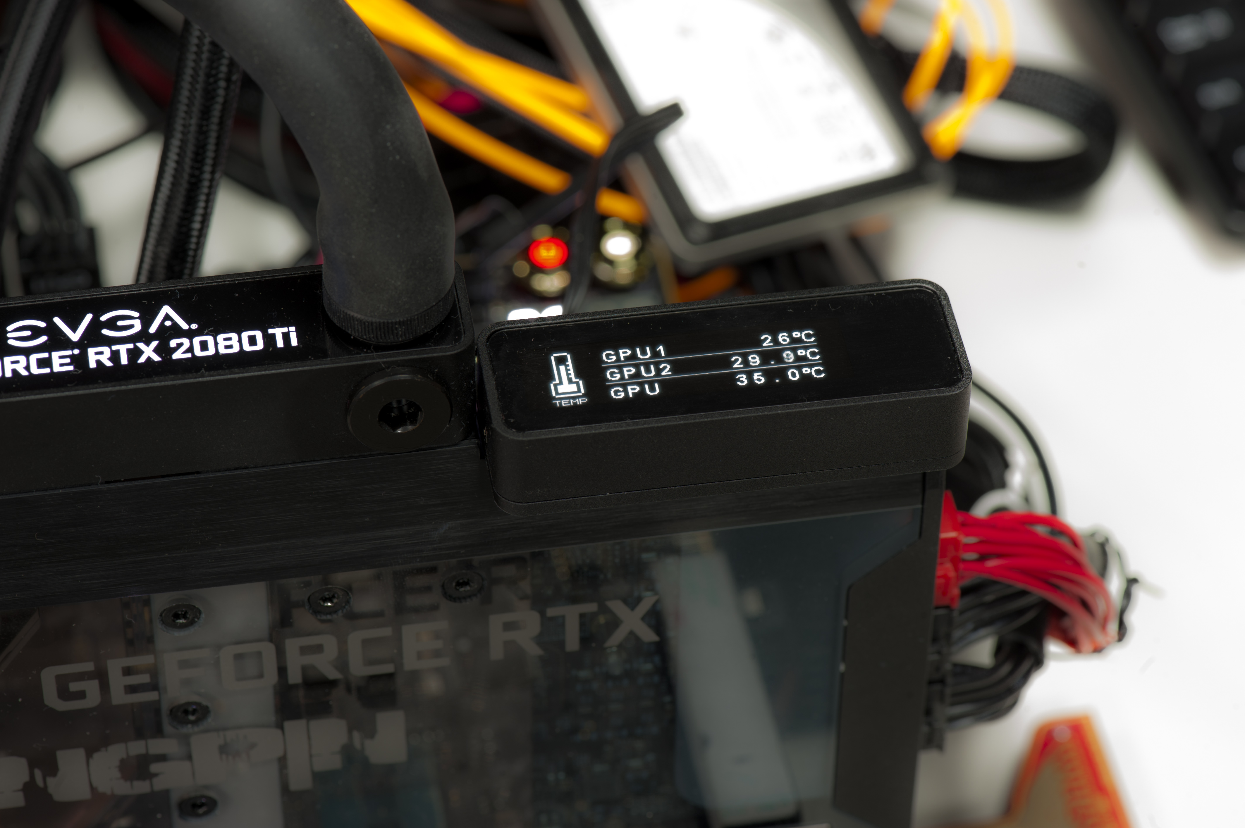
Reported temperatures idle (left image) and 20 minutes running TSX Stress test (right image). Reported temperature delta:
| Sensor | Idle temperature | TSX Stress temperature | Delta load-idle |
|---|---|---|---|
| GPU1 (Driver) | +26 °C | +39 °C | 13 °C |
| GPU2 | +29.9 °C | +40.6 °C | 10.7 °C |
| GPU Die Temp | +35.0 °C | +43.0 °C | 8.0 °C |
Depends on what sensor you use as reference, delta between loaded to idle temperatures vary from 8.0 °C to 13 °C.

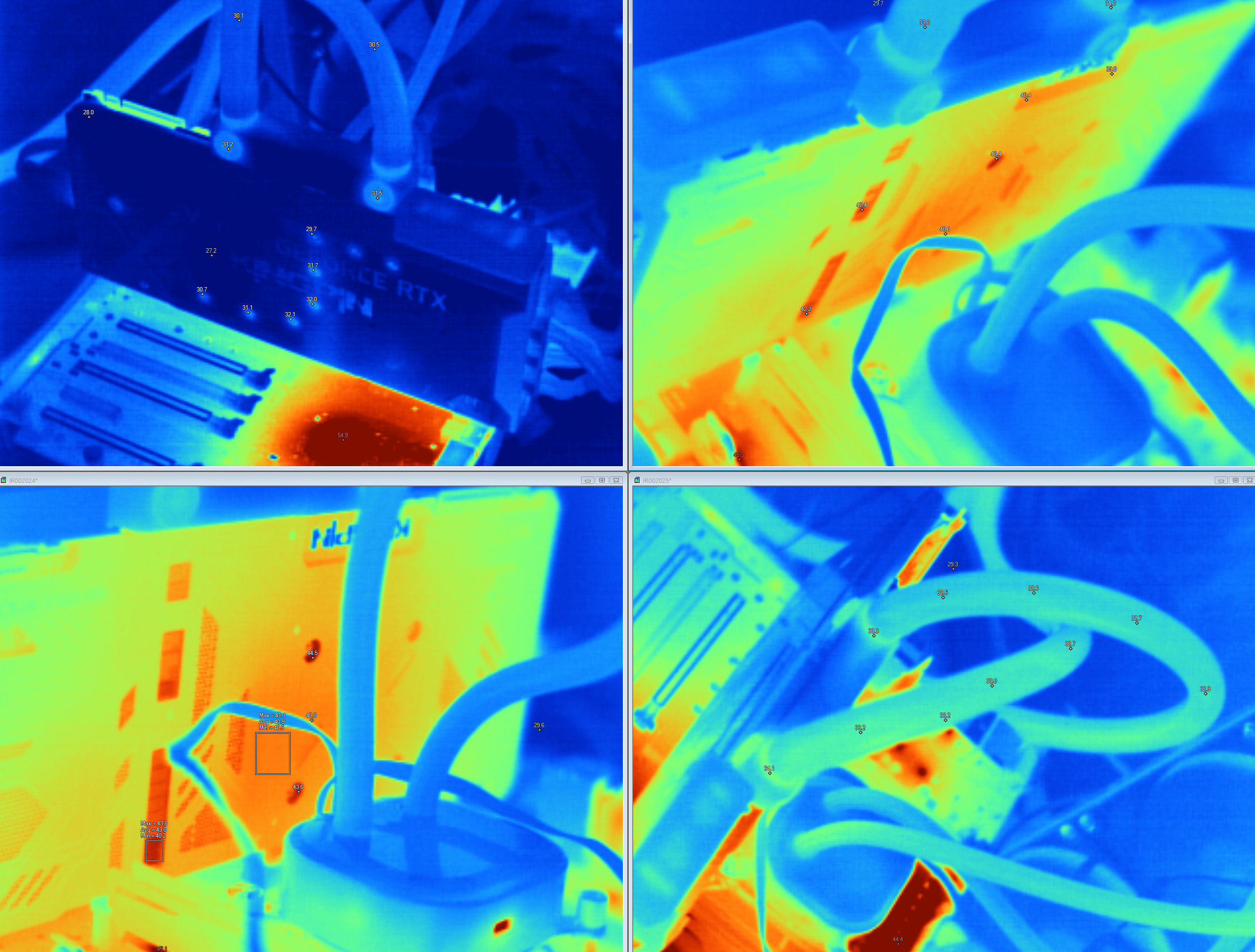
Some additional idea of the temperature gradients could be checked by thermal imaging. 8 thermal images below taken with Fluke Ti32 camera, with spot and area check markers. Click for large image to see details.
Finally 3Dmark TSX monitoring chart recorded during:
Temperatures impact on GPU overclocking headroom
Okay, now we have this glorious piece of hardware, with fancy watercooling to keep temperatures below +50 °C under load. That should be no limits to overclock TU102 GPU to absolute maximum, right? Wrong! Just like previous Pascal chips maximum stable clocks in this generation are still very sensitive to die temperature. If GPU cannot run X GHz at Y temperature, then little can be done to improve the situation other than reducing the Y temperature lower.
It is actually quite easy to test. Run last known stable clock (X minus 30 MHz, as example) in 3Dmark or other 3D application in loop mode. Wait till temperature reach stable state and then increase temperature +10 °C higher (for example by blocking airflow at the radiator). If card start crashing in result – one can measure how much this GPU gain MHz per each °C of headroom. Increasing voltages without improving cooling temperatures will often provide the opposite effect, as die temperature increase exponentially with elevated voltage. Ideally, best GPU will require the lowest voltage possible, while maintaining required clocks stable.
Table 7 illustrating actual frequency scaling in respect to temperature from one GPU in 3Dmark Port Royal test.
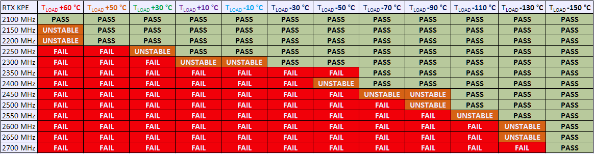
Table 7: GPU max overclocking scaling with temperature
Legend:
PASS = Card able to finish benchmark and produce a score
UNSTABLE = Card was running some time but crashed before the scene end or produce a lower score (thottled)
FAIL = Card did not start the benchmark or crash within 3 seconds
This is just single GPU result, to illustrate thermals impact on overclocking. This is same process as in Pascal and previous GPUs. Also with negative temperatures you would not want to go coldest possible, as the colder card runs, the more problems can happen due to water condensation and thermal stress. Pro 3D overclockers always try to maintain temperature just 5-10 °C below crashing point, so you can run the system for longer time, while running desired clocks.
In 24/7 daily overclocking using stock Hybrid or full-cover HydroCopper waterblock general suggestion is to leave GPU voltage alone and ensure good airflow in chassis to provide lowest possible GPU temperatures. Only if your cooling methods allow to keep load temperatures below +35…+25 °C you may need to think about voltages. GPU voltage starvation can be detected when GPU temperature under full load reduced 10-20 °C, but stable frequency is not increased and card still crashing.
LN2 Extreme OC cooling compatibility
EVGA200 PCBA does not have any tall components around GPU and memory area that would prevent installing aftermarket cooling solutions and extreme OC blocks. VRM heatsinks also zoned clear away from GPU area to meet these keep out requirements. You don’t need to chop capacitors or modify stuff to fit LN2 pot onto Kingpin edition 2080 Ti RTX.
Kingpincooling.com designed new extreme cooling container called ICON 3.0 that fits RTX 2080 Ti cards perfectly. It is a heavier unit to occupy dual-slot height and provide large surface contact for new GPUs like Titan V “Volta” and TU102 “Turing”. It is also backward compatible with older GPUs.
![]()
Image 58: Kingpincooling.com ICON 3.0 with RTX 2080 Ti KPE card
KINGPIN Edition RTX can go to the limit and are capable to hit 2600 MHz+ core frequency with the right amounts of voltage and stable subzero temperatures (-140°C or colder). Fully maxing out these GPUs on LN2 usually requires around -140 to -155c on the GPU container and roughly 1.40v-1.50v under load at DMM/monitor. The thermal grease you use and the mounting accuracy/pressure also has a very big impact on max clocks. It’s critical that the contact surface areas of the pot and the GPU are parallel and mounted with sufficient even pressure in all corners, or you can easily lose 200-300 MHz+ on top end.

Handling cryogenic liquids and cryogenic coolers can be dangerous and require personal protection equipment. LN2 is very cold substance, -196 °C (-320 °F) and can cause severe frostbite. Nitrogen’s critical point is -126.2 °C, as a result it cannot stay liquid at ambient temperature at any pressure. That means LN2 sealed in container will build up pressure and cause major explosion. LN2 also have gas to liquid ratio 700 to 1, which can displace all oxygen in the closed room and suffocate you without warning. Never use LN2 in a small, poorly ventilated room. Treat liquid nitrogen and any cooled object with respect.
This guide doesn’t cover extreme cooling insulation and condensation preparation of the card itself, as there are different ways to do this and everyone has a preferred method. The idea is to prevent any forming water condensation to come in contact with electronic circuits on the PCBA. Check around the usual OC-related internet forums or EVGA OC Lab for insulation/PCB preparation guides and tips for your graphics cards.
Once the PCBA is prepared, container mounted, and everything installed into the system you’re ready. ALWAYS do a quick post/boot at ambient temperatures before putting any LN2 or dry ice into the container just to be sure everything is still 100% functional on the card after you mounted it.

Image 59: Bare card with Kingpincooling.com KPx thermal grease applied.
Bad mounting and poor thermal grease for LN2 can cause a large temperature delta between the GPU pot surface and the die temp on the GPU itself. With 2080 Ti KINGPIN, there is an internal monitor for temperature die that can read down to -64 °C so you can actually check the delta of the card to see the contact accuracy and grease viability(frozen or not). Good delta (the difference between your thermometer measuring pot base and KPE GPU die temperature from OLED) would be less than 15 °C when GPU pot temperature kept around -40 °C. If you see larger delta, it is best to redo mounting or increase pressure of mounting nuts to provide better contact between LN2 pot base and GPU. Making good and flat contact between the two is CRUCIAL to top end GPU extreme overclocking.
Image 60: OLED in GPU die temperature monitoring mode
To display die temperature monitor on OLED, run PX1, go to OLED configuration setting page and choose GPU Die Temp sensor to display.
Check that the drivers are still working/installed, check for artifacts on the screen, even run a 3Dmark at default settings. If the container warms to 30-40 °C under load, just splash it with some LN2, don’t let it overheat is all you really need to worry about. If it can’t pass this test, it will never overclock on LN2 and getting past this part will ensure you won’t have to break down the rig after frozen and start over.
If everything is OK then let’s move on, but word to the wise: You can NEVER just pull the card down to minimum – temp (like -196 °C), set max voltage(1.6 V+) and think it will run alright. This is NEVER recommended and something I’ve always preached against since the very beginning. Impatience will lead to bad extreme overclocking sessions and likely ruined hardware. The proper way to overclock a VGA to the max clocks it can run is to go in steps, working your way up in voltage and down in temperature, like the following. Adjustable on the fly Vdroop changes can help when tuning in max clocks. Voltages shown are measurements taken at the Probe It reading point for core voltage:
| STEP 1, first 30-60 minutes | GPU ~2200 MHz | Default or 1.2-1.3V voltages |
| STEP 2, -40 to -60 °C | 2400 MHz | 1.3 VGPU, 1.45VMEM |
| STEP 3, -90 to -100 °C | 2450 MHz GPU, +1200-1300 MHz memory | 1.35 VGPU, 1.45VMEM |
| STEP 4, -120 to -140 °C | 2450-2500 MHz GPU, +1400-1500 MHz memory | 1.4 VGPU, 1.50VMEM |
| STEP 5, -160 °C and beyond | 2500-2600 MHz+ GPU, +1400-1500 MHz memory | 1.45V+ VGPU, 1.55VMEM |
| STEP 5, Warmup back to ambient | 2100 MHz / default | 1.3 VGPU, 1.45VMEM |
Table 8: Extreme overclocking steps and guidance for RTX 2080 Ti
These are the typical steps and LN2 scaling numbers of what many 2080 Ti KINGPIN cards can achieve with careful benchmarking. While this card is well capable to push TU102 GPU to its limits, the actual result still varies per specific GPUs behavior and system/configuration + benchmark used. Some benchmarks like Time Spy are hard on GPU, so they will reach lower maximum benchable frequency, while other like Port Royal stress more on memory, so you might need to fine tune settings to fit particular benchmark app. Other factors such as chip leakage, thermal grease quality and container mounting pressure can and will have visible impact on the end result.
Summary
There you have it, the 5th-generation Kingpin graphics card, now with RTX flavor to push performance higher than ever again. This project had a lot of design challenges and design decisions since the first prototype, so we are happy to finally get new KPE into your hands.
Happy benching and gaming! If you have any comments or question, join us in the comment section at the right side of this article or discuss at EVGA OC Forum.
Feel free to share and link to this guide, but keep links and all references intact, as this guide will be updated in the future as we have more information to share.
Projects like this are born from passion and a desire to share how things work. Education is the foundation of a healthy society - especially important in today's volatile world. xDevs began as a personal project notepad in Kherson, Ukraine back in 2008 and has grown with support of passionate readers just like you. There are no (and never will be) any ads, sponsors or shareholders behind xDevs.com, just a commitment to inspire and help learning. If you are in a position to help others like us, please consider supporting xDevs.com’s home-country Ukraine in its defense of freedom to speak, freedom to live in peace and freedom to choose their way. You can use official site to support Ukraine – United24 or Help99. Every cent counts.
Modified: June 29, 2026, 3:31 a.m.