Contents
Intro
NVIDIA Titan Volta graphics card released in the end of 2017 is quite a step ahead of usual mid-range GPU reference designs that released for new architecture first.
Base of this card is nerfed professional Tesla V100 PCIe , which is still very monstrous full-size 100-series GPU, Volta GV100. Unlike all previous NVIDIA Titan cards, this card is first to use on-package memory silicon, in form of Samsung HBM2.
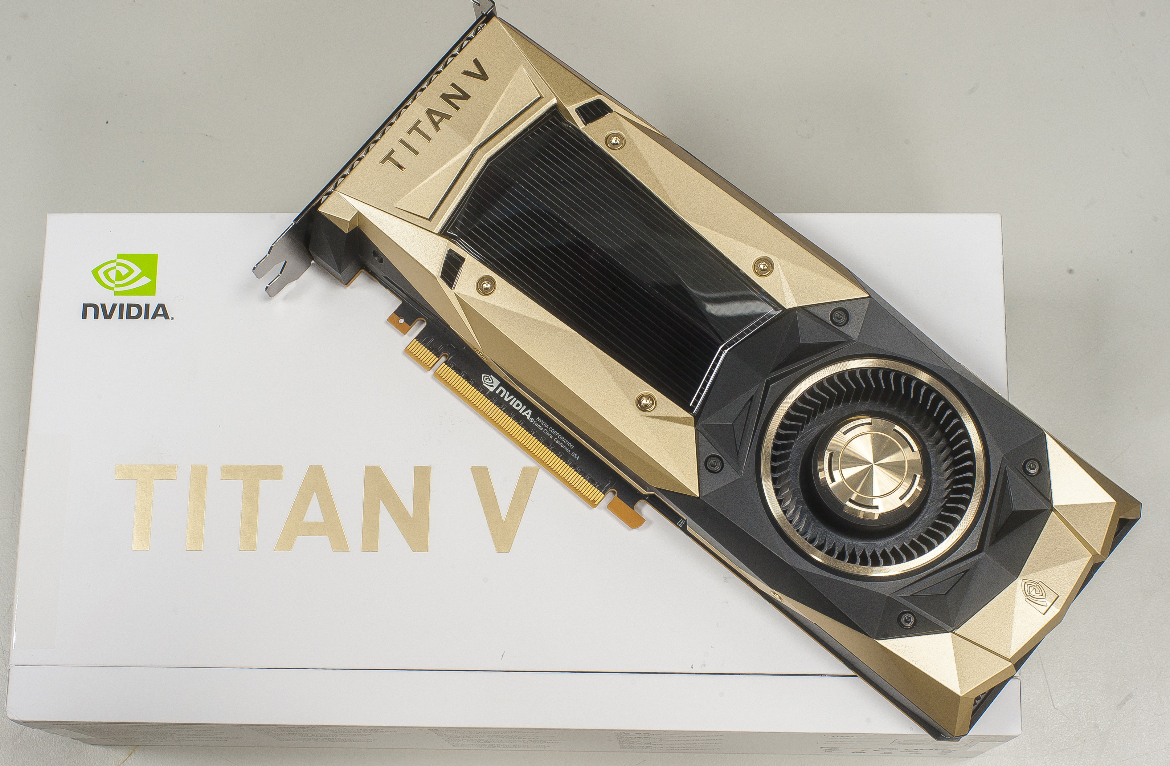
Image 1: Introduction to Titan V card
TechPowerUp’s GPU-Z since version 2.6 fully supports Titan V card as well, displaying all key information about the installed device.
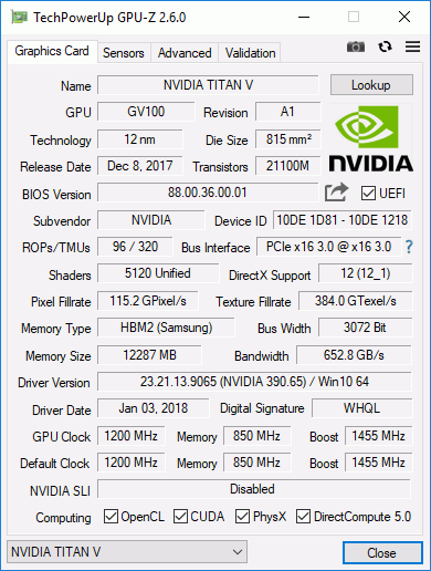
GPU-Z screenshot with Titan V card
Unlike previous OC guides, this article coverage is limited to technical overview for the time being.
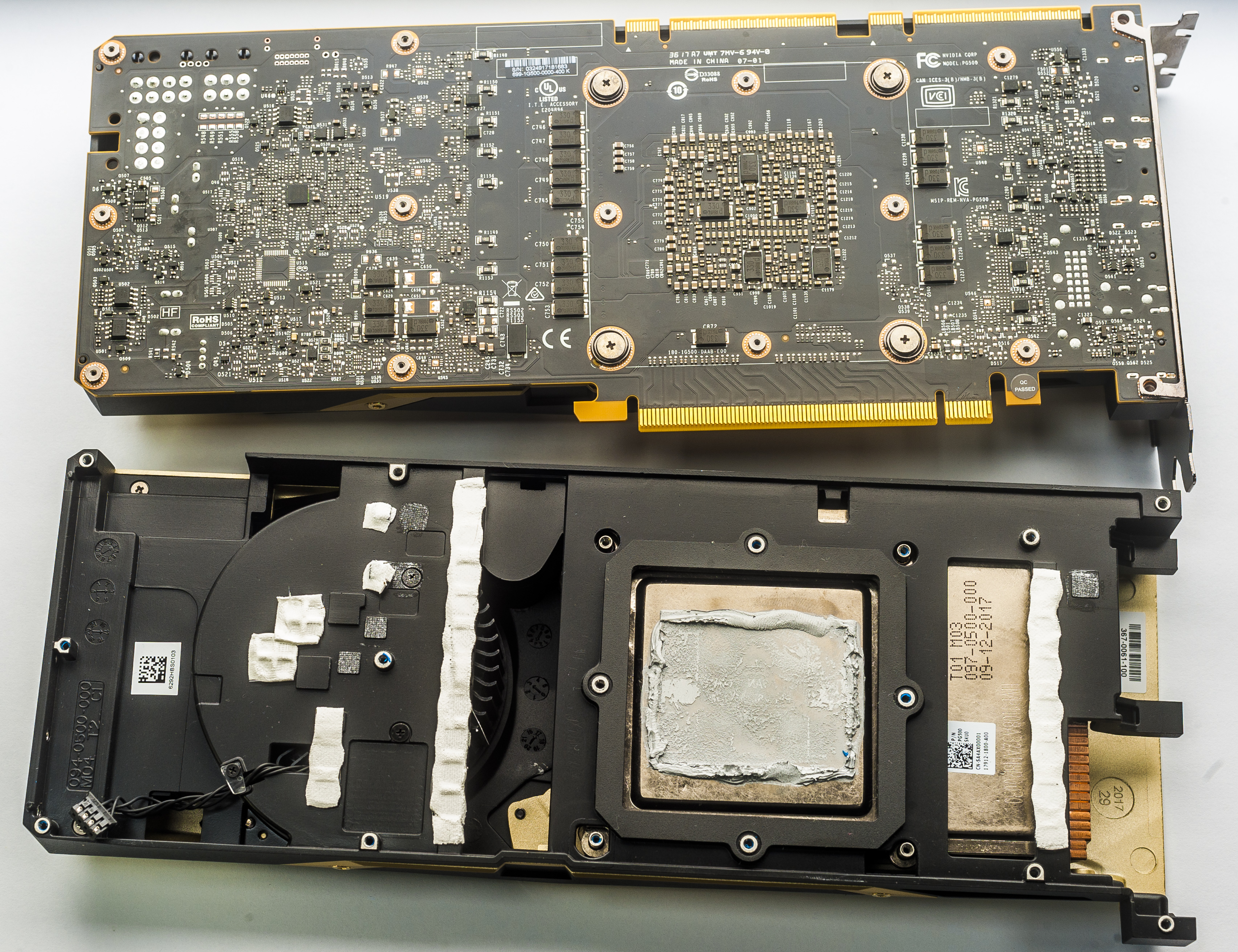
Image 2: Heatsink removal and naked board backside
I don’t expect many owners of this $3000 USD device to be interested in extreme overclocking of this thing, so there would be no advanced modifications this time.
Doesn’t mean we can’t try some fun with the card though. ;)
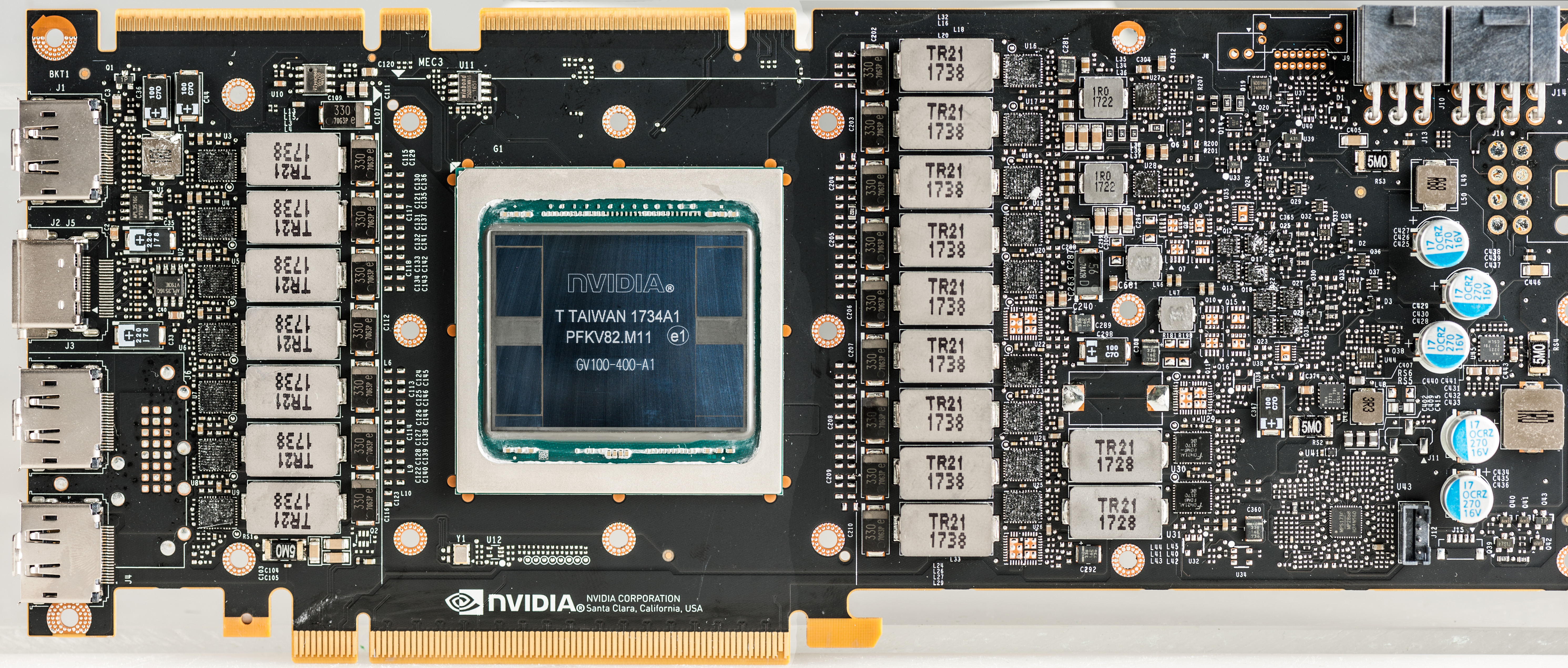
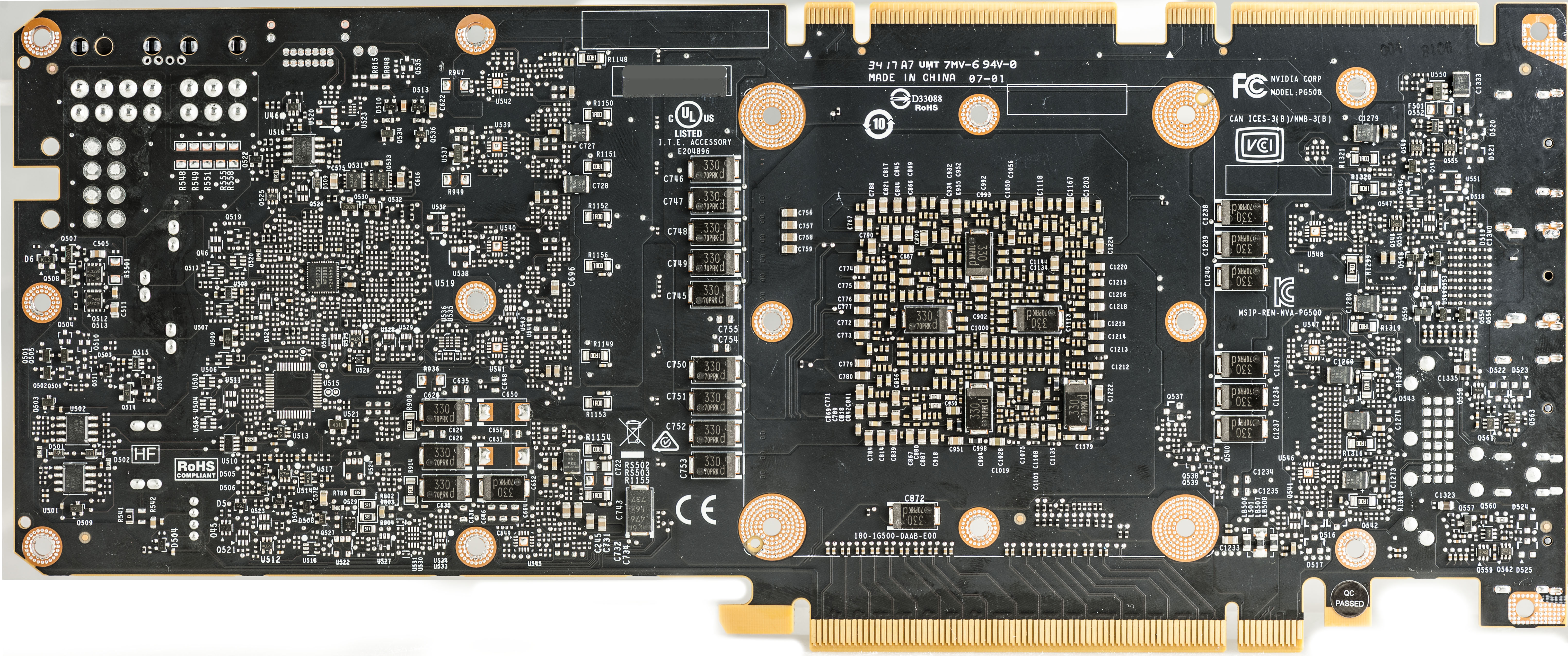
Image 3: Naked Titan V board in it’s glory
GPU itself is manufactured by TSMC fab in Taiwan. Four HBM2 memory stacks, with 4 GBytes in each of them are embedded on same package around the GPU. Unlike GDDR5/GDDR5X used on 10×0 series Pascal cards, GV100 connected to each memory cube thru 1024-bit wide I/O interface, forming total bus of 4096 bits. However one of the cubes is deactivated, rendering only 12GB and 3072-wide bus for Titan V. Fully featured chip with full memory capability is reserved for even more expensive professional adapters, like Tesla and Quadro.
Interesting theory brief and comparison to traditional GDDR type is available in this PDF presentation.
If you interested in more usual “uncork series” for previous GeForce cards, check them here:
- Reference GTX 1080/1070 – Uncorking Pascal
- Removing power limits on any NV card
- Dedicated EVGA EPOWER V DC-DC power regulator for VGA OC
- Using Raspberry Pi to control your VGA EPOWER VRM
- EVGA GTX 980 Ti K|NGP|N OC Guide
- Reference GTX 780/780Ti – Big KEPLER
- EVGA GTX 680 Classified – Uncorking guide
- Reference GTX 680 – Uncorking KEPLER
There are no custom AIB designs for this GPU, this design is strictly limited to NVIDIA-made product.
As usual, you are on your own alone, even when doing even little simple mod. If you card/system bursts in flames or just simply stop working, do not try to RMA it or expect a support from manufacturers. Anything below this paragraph in this article is NOT covered by any kind of warranty, and provided AS IS only for education purpose, without support from manufacturer or NVIDIA. So yes, “don’t try this at home”. Any RMA attempt of soldered card is easily diagnosed today and will be rejected.
No doubt, modifying your GFX for benchmarking and records require bit of above-minimal soldering skill knowledge and cold mind and sharp eye. Entry-level things, such as how to probe voltage/resistance with multimeter, what is trimpot and how to solder piece of wire, as these things were explained over the internet thousand times already and easy to google. If you need more info – also check previous guides, linked above.
Interesting to see that Titan V is also nerfed on memory bus width/size, similar to GTX 1080 Ti. Actual GPU have all 4 stacks of HBM2 silicon, routed 4096-bit memory bus on the package, but one stack is fused out/disabled. That’s happening to allow higher yield and avoid risk of cannibalizing Tesla Volta market. Titan V and Tesla V100 have same package and essentially are same card, just different configuration of active blocks/BIOS/driver support level.
Cooling compatibility
Due to much bigger chip package and different mounting holes dimension, this card is not compatible with pre-Titan V coolers. Heatsink use fin array made by copper, soldered to large vapor chamber to effectively dissipate heat from huge package, with combined GPU die + HBM2 stacks.
Main PCIe PCB is using advanced manufacturing process with laser buried vias and 12-layers HF material:

Image 4: GV100 side photograph, showing package material stack
NVIDIA GV100 package substrate using at least 16 layers, with 54 × 54 ball array size or so. It’s one of the largest BGA packages we see on compute electronics.
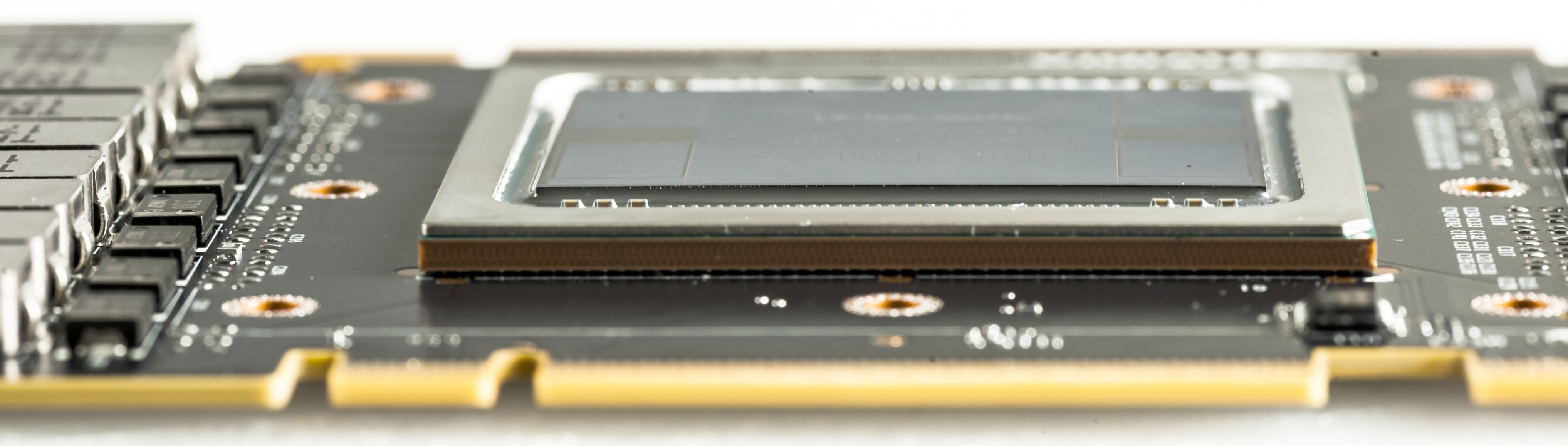
Image 5: Side angle view on GPU surface
Area around silicon dies filled with hard epoxy underfill , to protect fragile chips from mechanical damages.
STEP 1 – Prep your bench
Will need set of common tools for successful modding of reference Titan V card, which is similar to any other VGA.
- Card itself. Brand new Titan V used here to play with.
- 1 × 20 KΩ multi-turn VR (trim pot) for PLL mod.
- 3 × 2 Ω chip resistors, 0805 size. Example from Digikey, Mouser, Farnell DE for power limit mod.
- 25-45W soldering iron for trimpot mods.
- Roll of 28-32AWG insulated wire
- Soldering FLUX
- Kingpincooling TEK ICON container.
- DMM (I use fancy handheld Fluke 87V and high-performance Keithley 2002, but any 10$ DMM can fit needs of this guide)
- Low-ESR capacitors (2.5 or 4V rated, 680-820uF , etc) if you like to juice things up, but not required.
I had used ERSA iCON-1 soldering station with to cover all below. 102CDLF2.4 tip covered all trimpot mods for this guide, with temperature set to 290 °C. Before starting with soldering, clean the usual mess on table, get all tools checked and ready, turn on enough lights to clearly see all those tiny parts on PCB. Worth to ensure enough space around, so you don’t knock other stuff by accident. Also worth to take a close look on PCB layout from both top and bottom sides, to get familiar with location of key components and design.
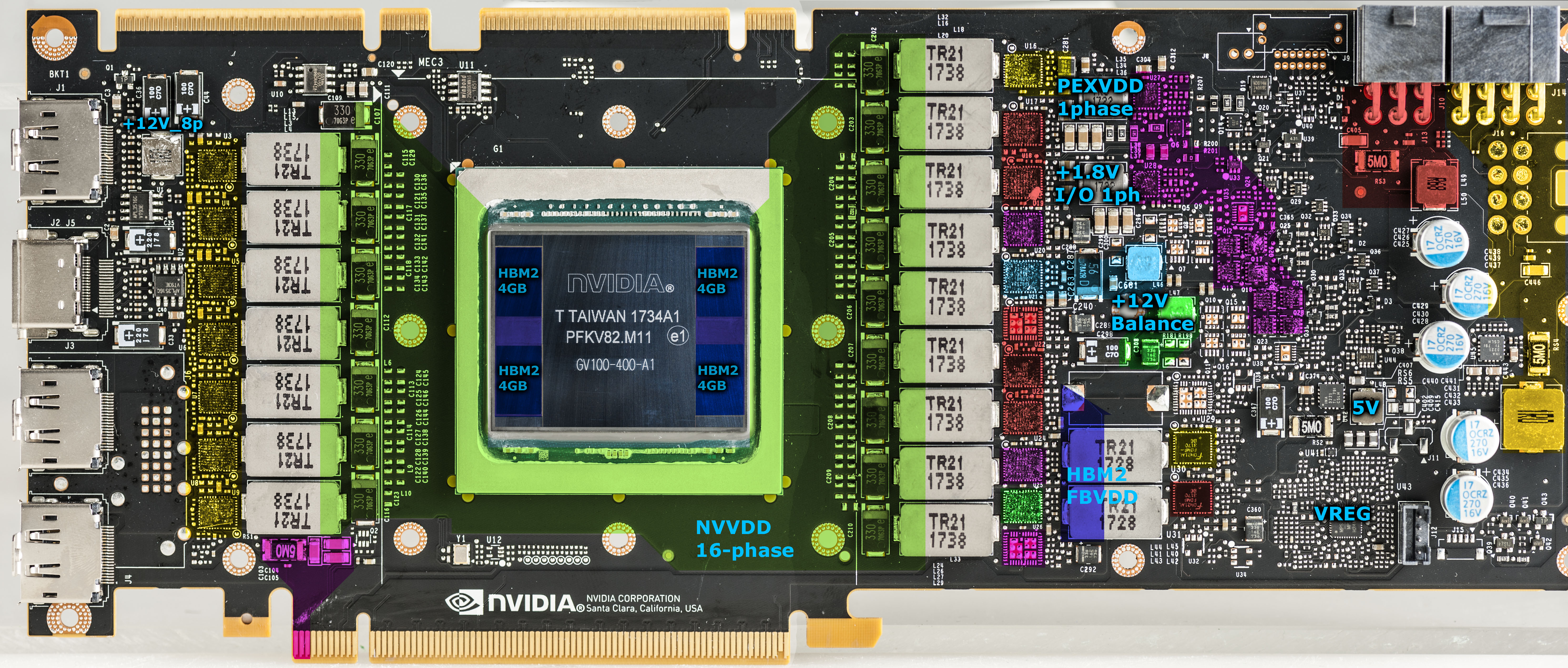
Image 6: Titan V VRM section colored for clarity on reference board
GPU bears GV100-400-A1 marking, which tells you it’s huge 100 series processor (to remind you, GTX 1080Ti based on GP102, Titan X Pascal use GP102-400, pro Tesla V100 with HBM2 – also GV100), silicon revision A1. It was manufactured by TSMC Taiwan. There are some 0201 decoupling capacitors around GPU die to help with power delivery. No hidden jumpers, traces or test points are visible on the package elsewhere, so nothing to worry about unlocking. SLI connectors are now gone, and replaced with dual NVLink x16 lane headers. PCIe connector for Gen3 host link look exactly same as before, no Gen4 magic here yet.
Multi-GPU SLI technology on Titan V is NOT supported, so EVGA 1080 Ti KPE still holds 3Dmark world records with 4-way SLI setup.
STEP 2 – Get card ready
Remove cooler from the card, since access to both sides of PCB for modifications is required. This time NVIDIA did not use TORX-type screws, so usual Philips and suitable size hexagon driver will do just fine. Avoid using pliers as those little components and resistors around are very easy to get damage if tool snaps. You will need hexagon driver to remove nut-head screws which used to hold backplate and PCB together.
Better keep all those custom screws in secure place somewhere, so you can put heatsink back after you done if you will decide to do so. Remember, after soldering your warranty will be surely violated, as every RMA center will easily see non-factory soldering specks, even if you very careful.
Now graphics card is exposed and ready for some measurements and modifications. I’ll spare our readers from boring part of measuring various points to find out what we need and where different connections go, so we can jump right into good stuff, starting with removing power cap limitations.
STEP 3 – Power limit overrides
Often gamers and users are mistakenly referring to 6-pin or 8-pin MiniFit.JR connectors as 75W or 150W capable inputs. Nothing can be further from truth. These power levels are nothing but just way for NV determine how capable is used board hardware in terms of power delivery system. It’s imaginary target number and have nothing to do with actual power taken from connector nor power input capability. Software and NV BIOS will handle GPU clocks and reduce voltages if measured power hitting programmed BIOS limit (which can and usuall is different value than 75/150W per connector!).
If you intend to do serious overclocking and benchmarking, it may be required to trick power monitoring circuitry to report lower power reading, so you not run into power throttle. Also to make sure we are not at any physical limit of power connector itself, check Molex 26-01-3116 specifications, which have specifications both 13A per contact (16AWG wire in small connector) to 8.5A/contact (18AWG wire).
This means that using common 18AWG cable, 6-pin connector specified for 17A of current (3 contacts for +12V power, 2 contacts for GND return, one contact for detect). 8-pin have 25.5A current specification (3 contacts for +12V power, 3 contacts for GND return and 2 contacts for detection). This is 204W at +12.0V level or 306W for 8-pin accordingly.
Now if somebody tells you that 6-pin can’t provide more than 75W, you know they don’t understand the topic very well. It’s not the connector itself or cable limit the power, but active regulation of GPU/BIOS/Driver according to detection of used cables and preprogrammed limits. So now we getting to know how actual power measured?
Just like GTX 1080 FE card is also using already known Texas Instruments INA3221 sensor IC, which is triple-channel monitor able to measure voltage, current and power on +12VDC input rails using just few external components and current shunts. Current shunt is special type of resistor which generate little, but measurable voltage which closely depends on amount of current flowing thru it. Thus card can detect power consumption in real-time and adjust its clock speed and performance automatically to keep power within specified envelope.
You can find current shunts which are marked RS1, RS2, RS3, RS4 on PCB with black resistive element in center and often with 005 or R005 or 5M0 mark on top. Sometimes there are no marks, but look is always very similar, like a large rectangular flat part with two or four wide metal terminals. Usually these shunts are located very close to input power connectors before the main VRM circuitry. If we manage to reduce voltage signal (which is in linear dependance from current) from these shunts, then reported power limit will be reduced as well. Don’t do anything with these shunts, just understand what they are for. Common “modifications” like applying liquid metal paste or using pencil are bad idea, as they do not provide reliable and static resistance change. Pascal cards have also protection against under-reporting, meaning that GPU will be stuck in low power state if reported power is zero or around that.
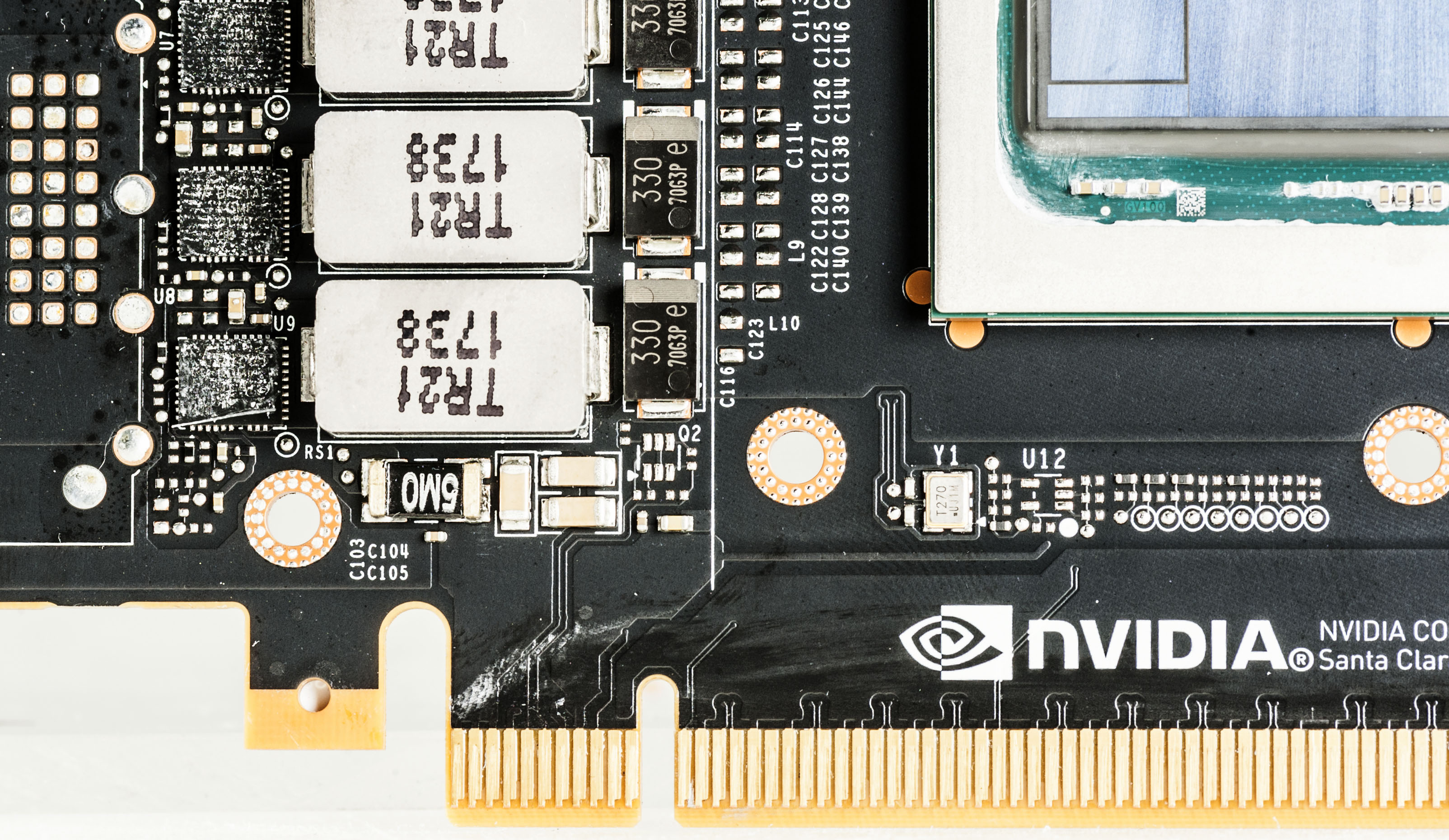
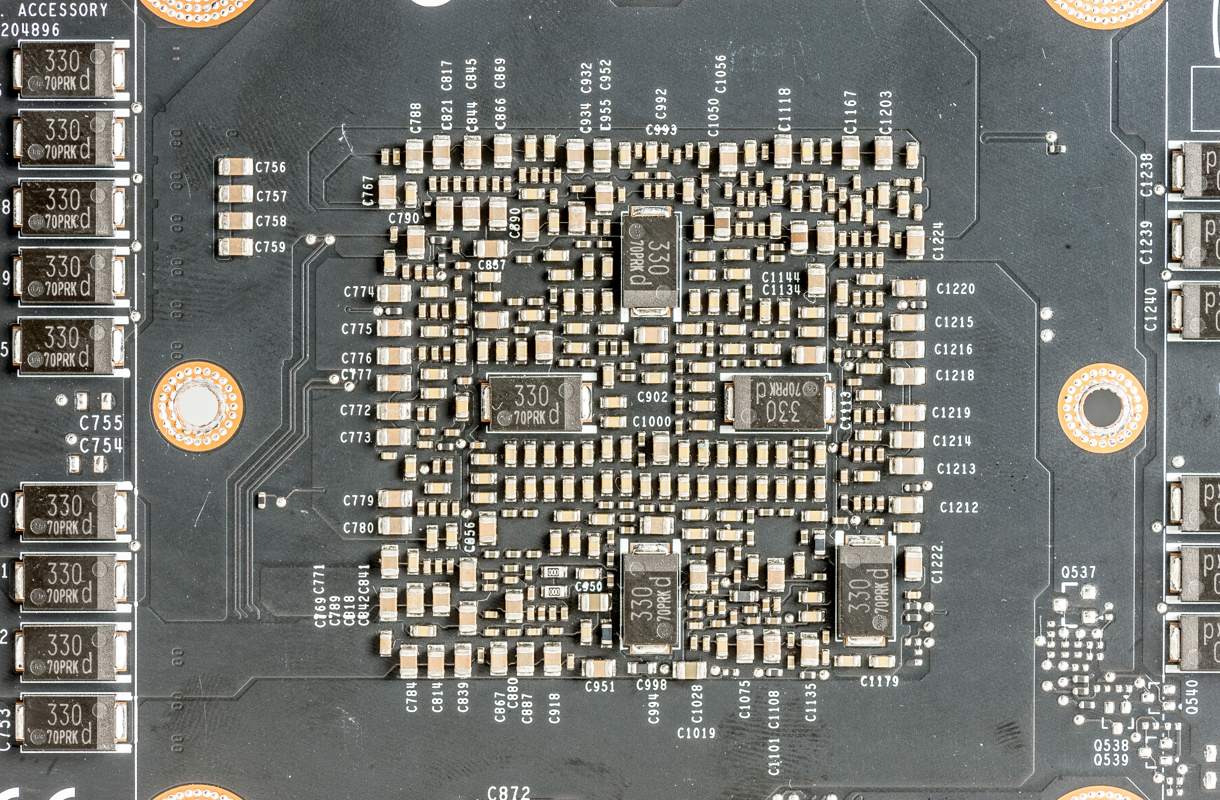
Image 7-8: Titan V PCIe power entry and backside decoupling caps
Adding 2-5Ω 0805 size resistor on top of every larger ceramic capacitor next to INA3221 U42,U45 will reduce power levels about x3 times. These chip resistors can be bought in usual electronics shop, or online at retailers like Digikey, Mouser. In worst case you still can use usual thru-hole resistor, but it’s not as convenient and you risking damaging caps or ripping traces off the board if you apply physical force on the joints.
I don’t show actual photo of this mod, as it’s nearly the same as in GTX 1080 case. This modification also very similar for all other NVIDIA cards, with bit more details covered here and here before.
First and usually most viable modification is one to adjust GPU core voltage. Often (but not always!) extra voltage can help to get better stability and higher clocks, given no temperature or power limitations are hit. Maximum available voltage thru software only control on reference cards are very limited, so hence you may need hardware modification to achieve higher voltages.
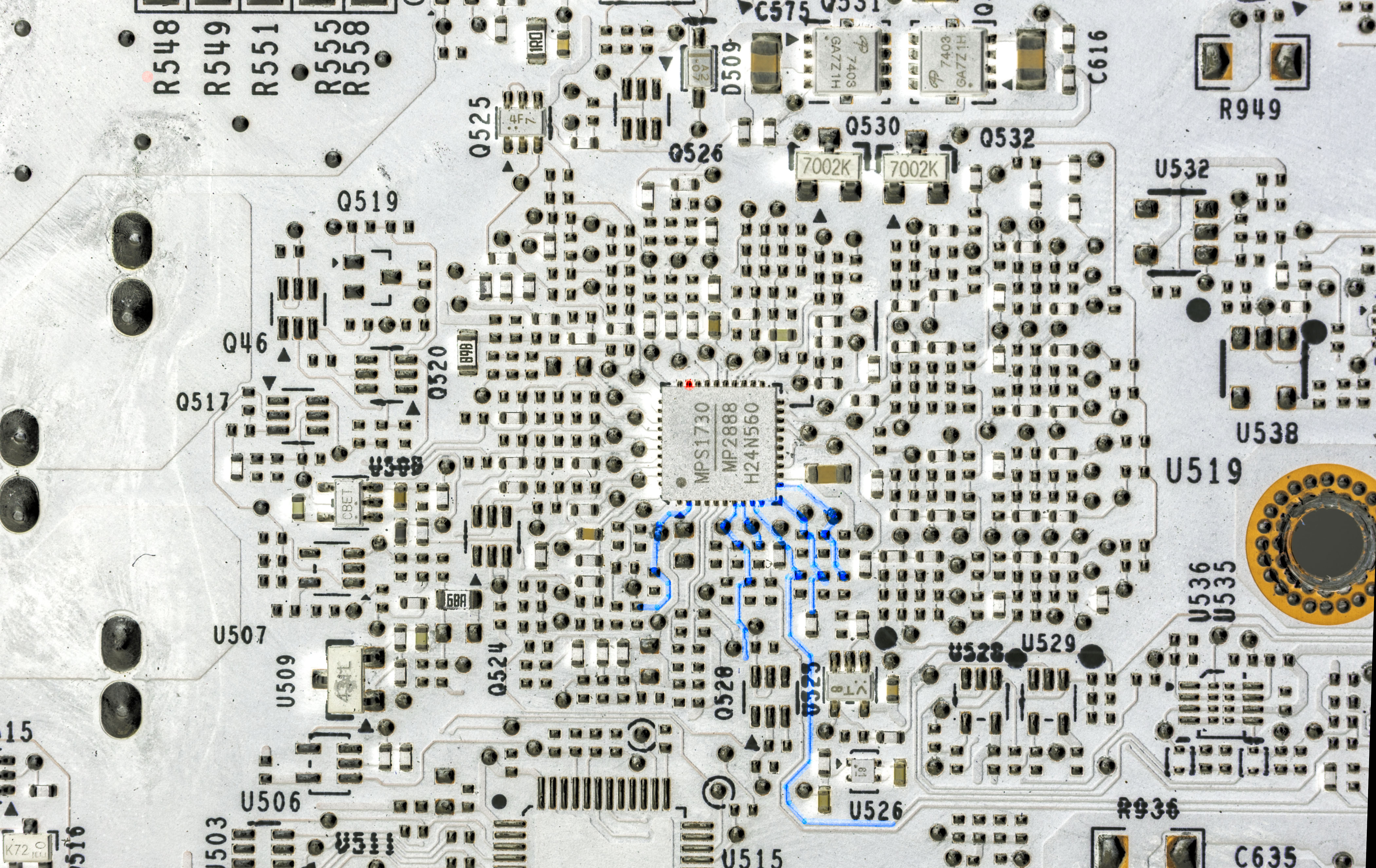
Image 9: Titan V VCORE VRM section. Blue lines are PWM LX nodes, red dot is feedback?
Here are two photos of main power controllers, which is same MPS MP2888. There is no public datasheet available for these.
Since traces and solder points on PCB are very thin and easy to peel off, make sure you fix the wire to PCB in few places, so it does not move. I found use of few cyanoacrylate superglue drops on areas free from components good enough. This will ensure modification is safely secured and will not rip apart tiny components so easy.
Note that GPU resistance on Volta GPUs is very low, same as Pascal generation. I measured it around 100 mΩ (that is 0.1 Ω), depending on GPU sample. Measurement was done using four-wire resistance measurement method with expensive high-accuracy Keithley Model 2002 DMM.
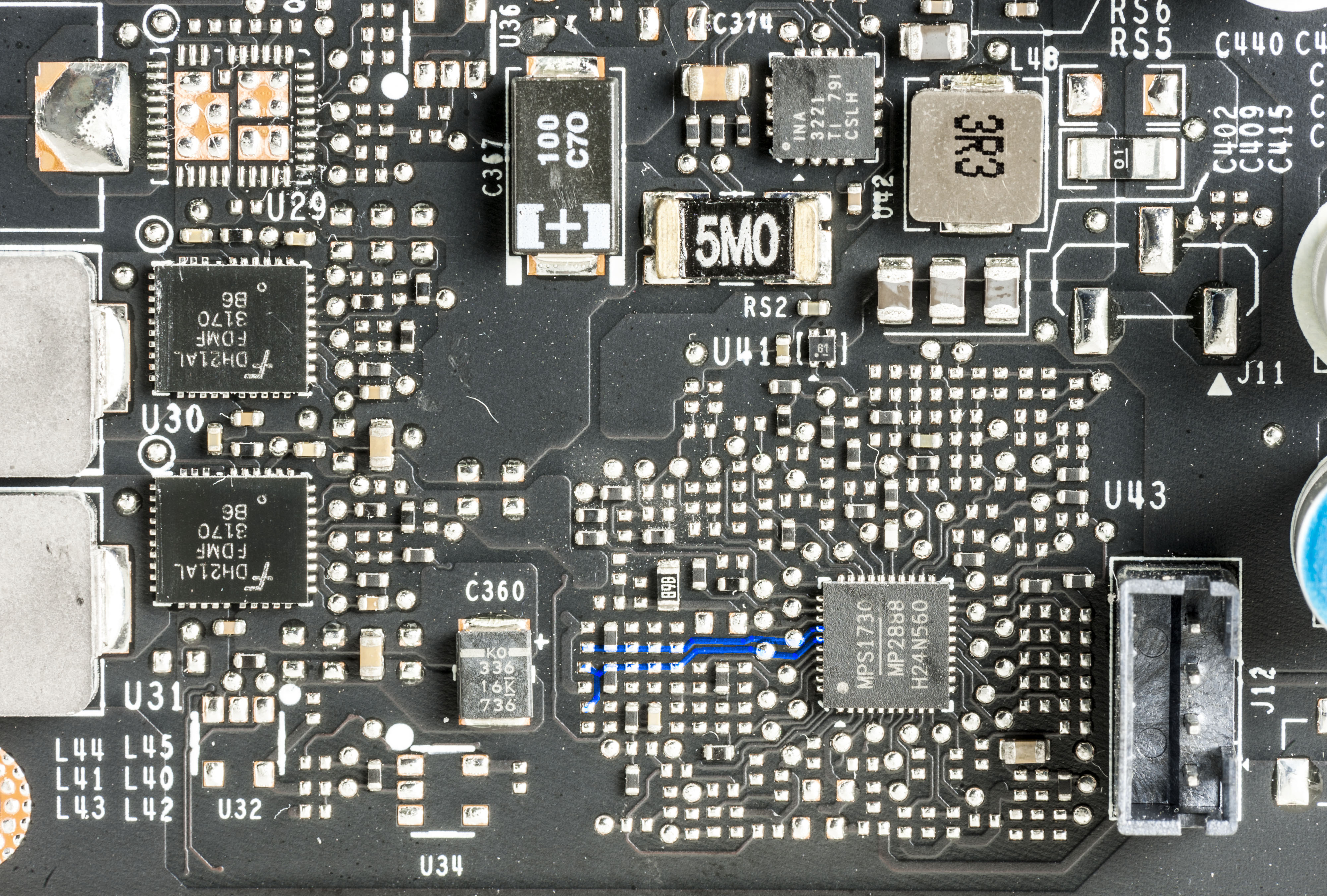
Image 10: Memory VRM with digital I2C lines in blue.
PLL regulator is common and known from previous GPUs, so nothing new here. PWM chip used is GStek GS9230 in small DFN package. Modification to raise voltage on it is straight forward and involve connection of 20KΩ trimmer to GND and pin 5 node.
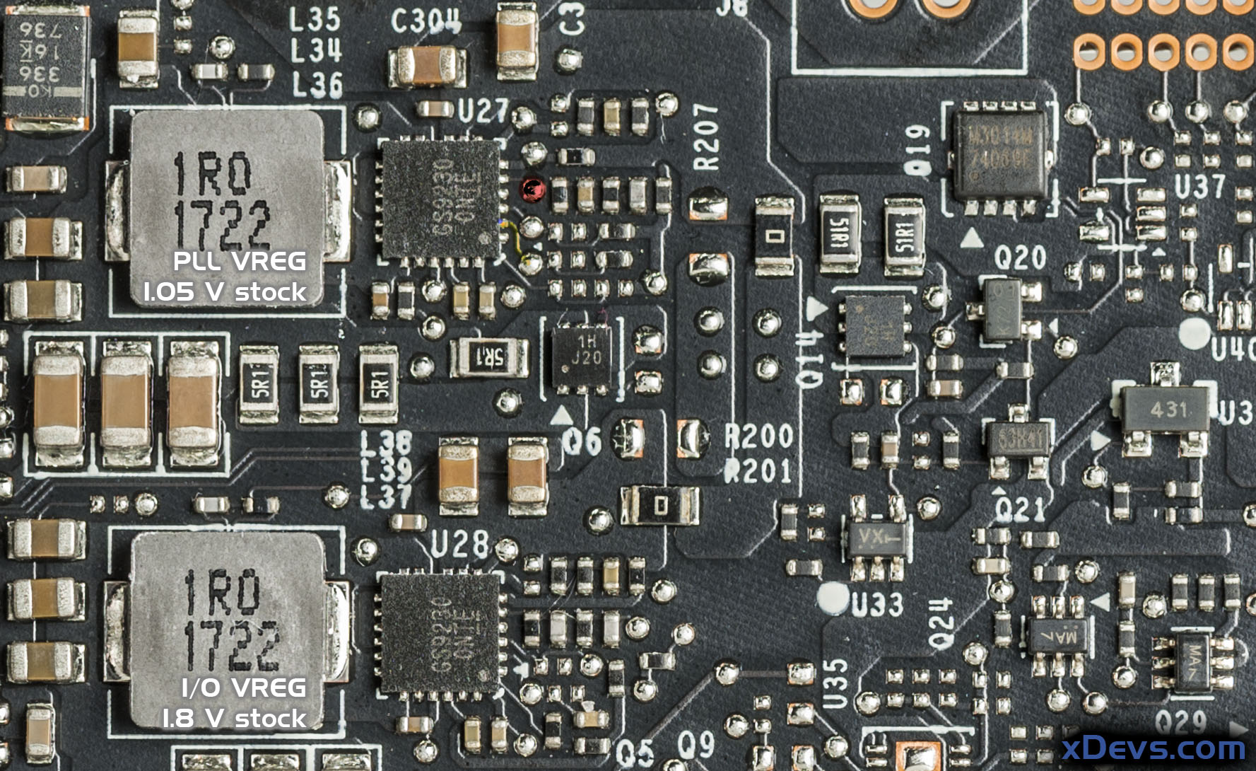
Image 11: PLL voltage regulator area and feedback point
Monitoring of PLL voltage output can be done by soldering wire to the marked point near PLL regulator.
Now everything is finally ready for some serious testing. Make sure you start with little voltage adjustments first and note all steps as you go higher and higher. This will help you to understand how voltages and things affect stability and make further overclocking easy.
Best to have full 8-points bracket mount to ensure good and even mount pressure across all GPU sides.
This card is compatible with ONLY new TEK ICON containers and can be bought separately on Kingpincooling.com shop. Older TEK9 FAT will not work, because GPU die size and mounting is much bigger.
Extra capacitors may or may not help to push higher clocks. Up to you to find out that.
Check again, if everything good, no shorts on the card or damaged parts, solder blobs or dirt. Make sure all trimpots are set to proper value.
Assemble your cooling solution to a card, test voltages and give it a spin on overclocking, using EVGA Precision XOC 16.
Also here are reference points, key resistance values measured with high-accuracy Keithley 2002 DMM on good working card:
| Voltage rail | Resistance measured | Nominal voltage |
| NVVDD | ~100 milliΩ depends on card | 0.62 VDC … 1.00VDC |
| FBVDD | ~30-40 Ω depends on card | 1.36 VDC fixed |
| PEX | ~40-70 Ω depends on card | 1.015 VDC fixed |
Table 1: Nominal resistance on main power rails from good Titan V card
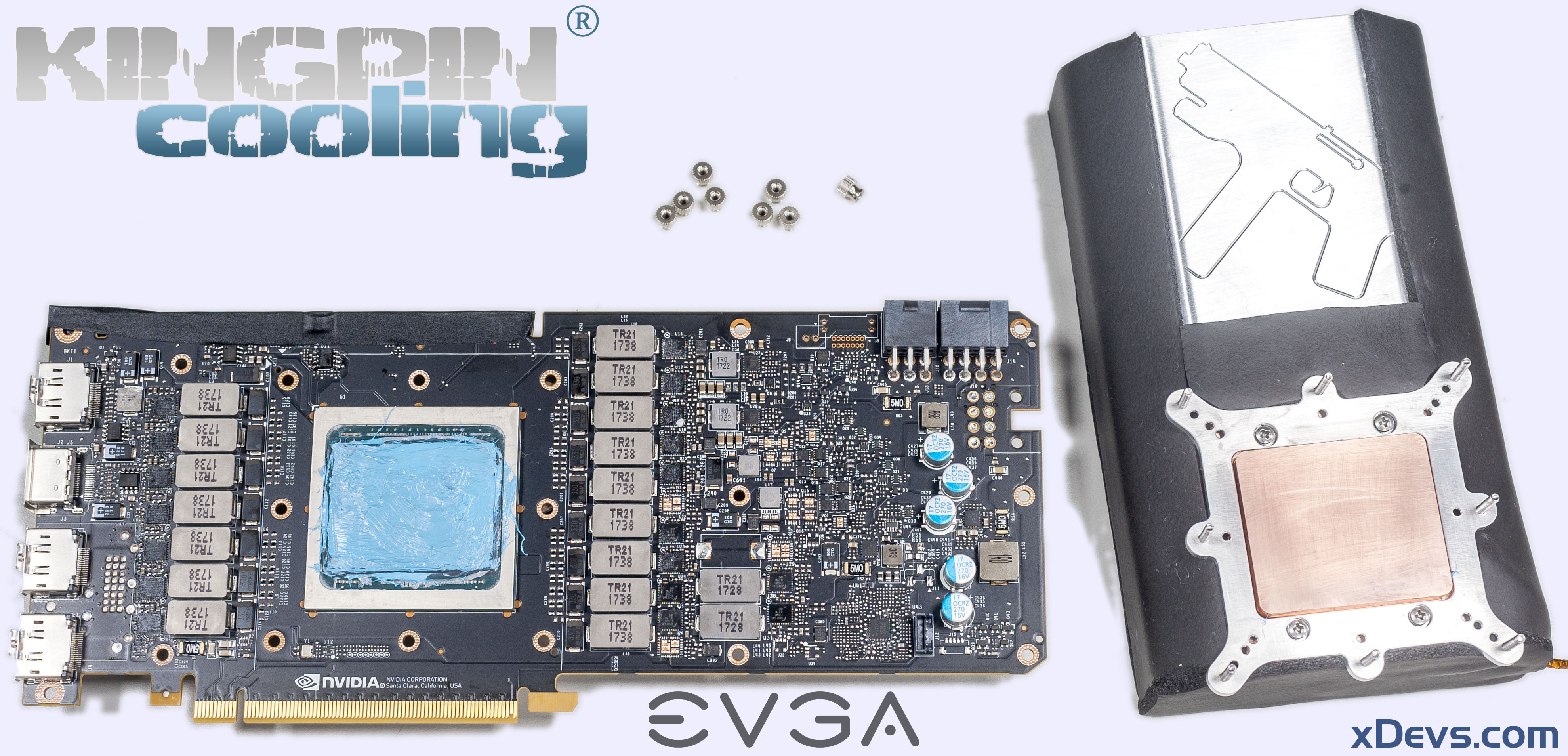
Image 12-13: Titan V ready to go with Kingpincooling.com TEK prototype container
If you get very different (less than 30 mΩ) resistance readings, you card is likely borked and game is over.
Image 14: Titan V frosty after the test session
As usual, any feedback and questions are appreciated. Feel free to share link to this guide, but keep links and references intact, as guide likely to be updated in future.
Projects like this are born from passion and a desire to share how things work. Education is the foundation of a healthy society - especially important in today's volatile world. xDevs began as a personal project notepad in Kherson, Ukraine back in 2008 and has grown with support of passionate readers just like you. There are no (and never will be) any ads, sponsors or shareholders behind xDevs.com, just a commitment to inspire and help learning. If you are in a position to help others like us, please consider supporting xDevs.com’s home-country Ukraine in its defense of freedom to speak, freedom to live in peace and freedom to choose their way. You can use official site to support Ukraine – United24 or Help99. Every cent counts.
Modified: Jan. 5, 2023, 1:07 a.m.