- Intro
- Disclaimer
- Manuals
- Design and construction
- Initial check and external interface
- Troubleshooting
- Thermal sensor diagnostics
- Calibration
- Summary & Conclusion
Intro
In this article we will take a look and perform service of high-end AC Voltage Measurement instrument, Fluke 5790A. Fluke 5790A is precision instrument to perform unknown DC and AC voltage measurements with the uncertainty of a metrology grade thermal transfer standard. Initial condition, reported by unit’s owner – permanent overload error message HHHHHHHH on the screen, with any range, including 1kV. Condition is same with no signal at the inputs, or even shorted input. There was no history available how the issue developed, so we can perform troubleshooting and check for any problems or component damage. Given the fact, that owner environment involve design and verification high-power AC/DC sources and similar industrial high-energy equipment, I’d assume that 5790A’s input was overloaded by such source.
The Fluke 5790A AC Measurement Standard today is already replaced by face-lift version Fluke 5790B both of which are share same chassis and architecture.
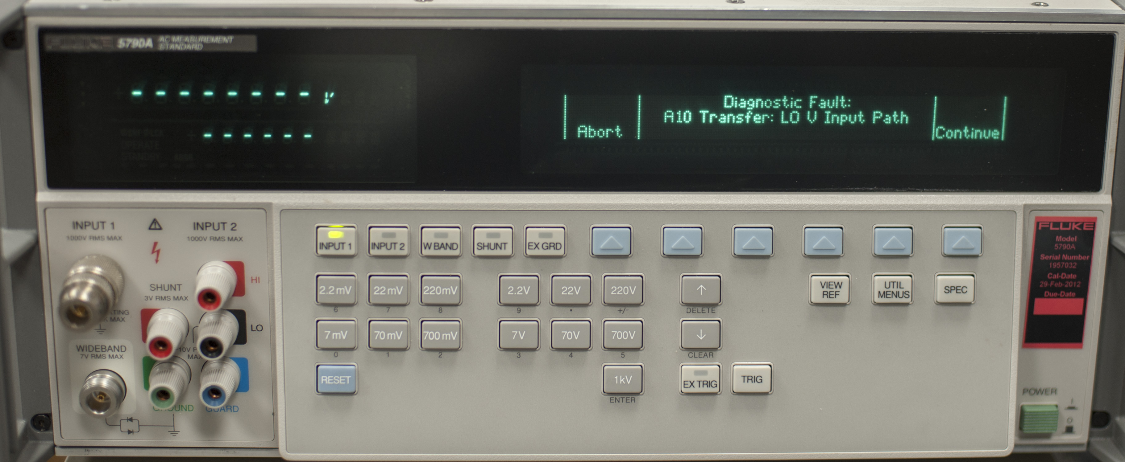
Image 1: Sick Fluke 5790A
5790A can perform direct measurements of unknown signals or perform relative transfers between known and unknown input signal. In measurement mode, the Fluke 5790A operates as a digital accurate AC voltmeter with up to 8 digits of resolution. Measurement mode uses an internal stable DC reference to compare with unknown AC input.
In transfer mode, external DC or AC reference source can be supplied to unit to perform a comparison. The 5790A automatically performs switching and calculations, and displays the resulting AC-DC or AC-AC difference. The 5790A has multiple input voltage ranges, with acceptable signal levels from 700 µV to 1000 V (70 mV minimum in transfer mode), and a frequency range of 10 Hz to 1 MHz. A wideband option allow frequency range extension to 30 MHz, however unit we study today have base configuration without WB option. The 5790A is also compatible with Fluke A40 current shunts, which allow to make AC-DC or AC-AC current transfer measurements up to 20 Amp.
Disclaimer
Redistribution and use of this article, parts of it or any images or files referenced in it, in source and/or binary forms, with or without modification, are permitted provided that the following conditions are met:
- Redistributions of article must retain the above copyright notice, this list of conditions, link to this page (/fix/f5790a/) and the following disclaimer.
- Redistributions of files in binary form must reproduce the above copyright notice, this list of conditions, link to this page (/fix/f5790a/), and the following disclaimer in the documentation and/or other materials provided with the distribution, for example Readme file.
All information posted here is hosted just for education purposes and provided AS IS. In no event shall the author, xDevs.com site, or Fluke or any other 3rd party be liable for any special, direct, indirect, or consequential damages or any damages whatsoever resulting from loss of use, data or profits, whether in an action of contract, negligence or other tortuous action, arising out of or in connection with the use or performance of information published here.
If you willing to contribute or have interesting documentation to share regarding pressure measurements or metrology and electronics in general, you can do so by following these simple instructions.
Manuals and service information
Fluke 5790A Operator manual January 1992 Rev.4, 8/12
Fluke 5790A Operator manual January 1992 Rev.3, 10/94
Fluke 5790A Remote Programming Reference Guide January 1992
Fluke 5790A Remote Programming reference guide
Fluke 5790A Instrument Security Procedures
Fluke 5790A Service Manual January 1992 Rev.5, 1/07
Fluke 5790A Service manual January 1992 Rev.4, 2/94
Fluke 5790A/AF AC Measurement Standard Addentum
Few additional applications notes:
Verifying the Wideband Input of an AC Measurement Standard
A New Method for the Calibration of the mV Ranges of an AC Measurement Standard
Design and construction
The 5790A AC Measurement Standard is designed as complete device to perform automated AC-DC transfers and for use as laboratory standard. All measurements are automated by internal microprocessors, so use of the AC measurement standard is simple as typical DVM. However unlike more general purpose DVM and DMMs, Fluke 5790 purposed to do Alternating voltage (AC) measurements. The following elements are among those critical to establishing the high accuracy of the 5790A. Core of the performance is custom Fluke designed thermal sensor hybrid.
- The FTS is the transfer element. It compares a precisely known internally generated DC voltage (or a low frequency square wave derived from DC) to an unknown AC voltage. If the FTS output remains unchanged when the input switches from the unknown AC voltage to the known DC voltage, the RMS value of the AC voltage is equal to the DC voltage. The FTS has extremely flat frequency response and has short term stability approaching 1 ppm.
- Highly stable thin-film resistor networks scale the 7 V range and higher to the FTS 2 V operating level and to scale the precision chopped reference to the 0.7 mV level.
- An ADC to measures the FTS output voltage and compare with known DC level.
- A high-resolution very linear DAC (digital to analog converter) generates precisely variable DC for the AC-DC transfer.
- An ultra-stable DC voltage reference based on two Linear/Fluke LTFLU-1ACH ovenized reference module establishes long-term DAC accuracy and low noise.
- A DC-to-square-wave converter chops the DAC output to eliminate DC reversal error in the RMS sensor.
Initial check and external interface
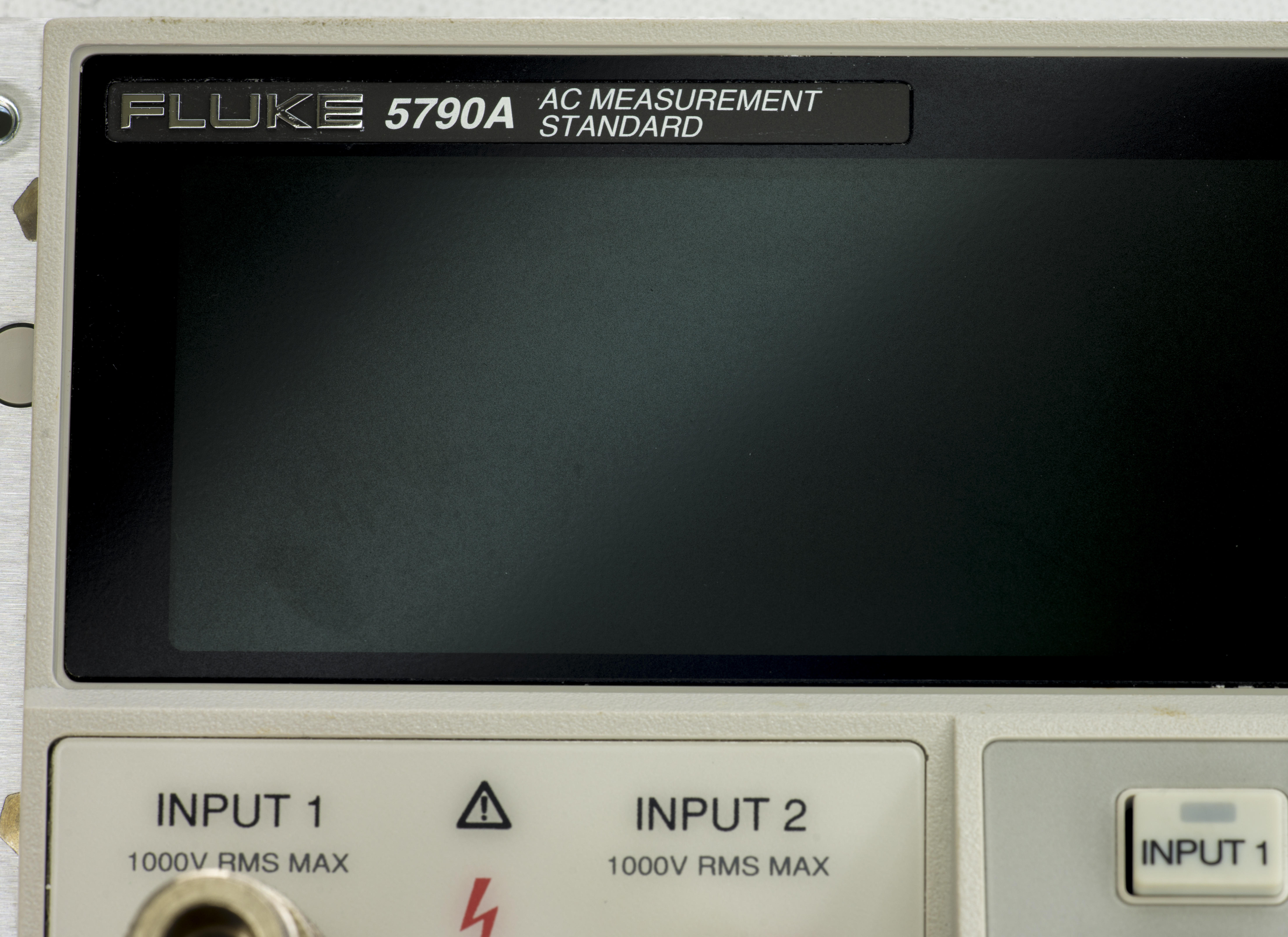
Front panel and chassis repeat design of Fluke’s 57xx-series multifunction calibrators, such as 5700A.
 |
 |
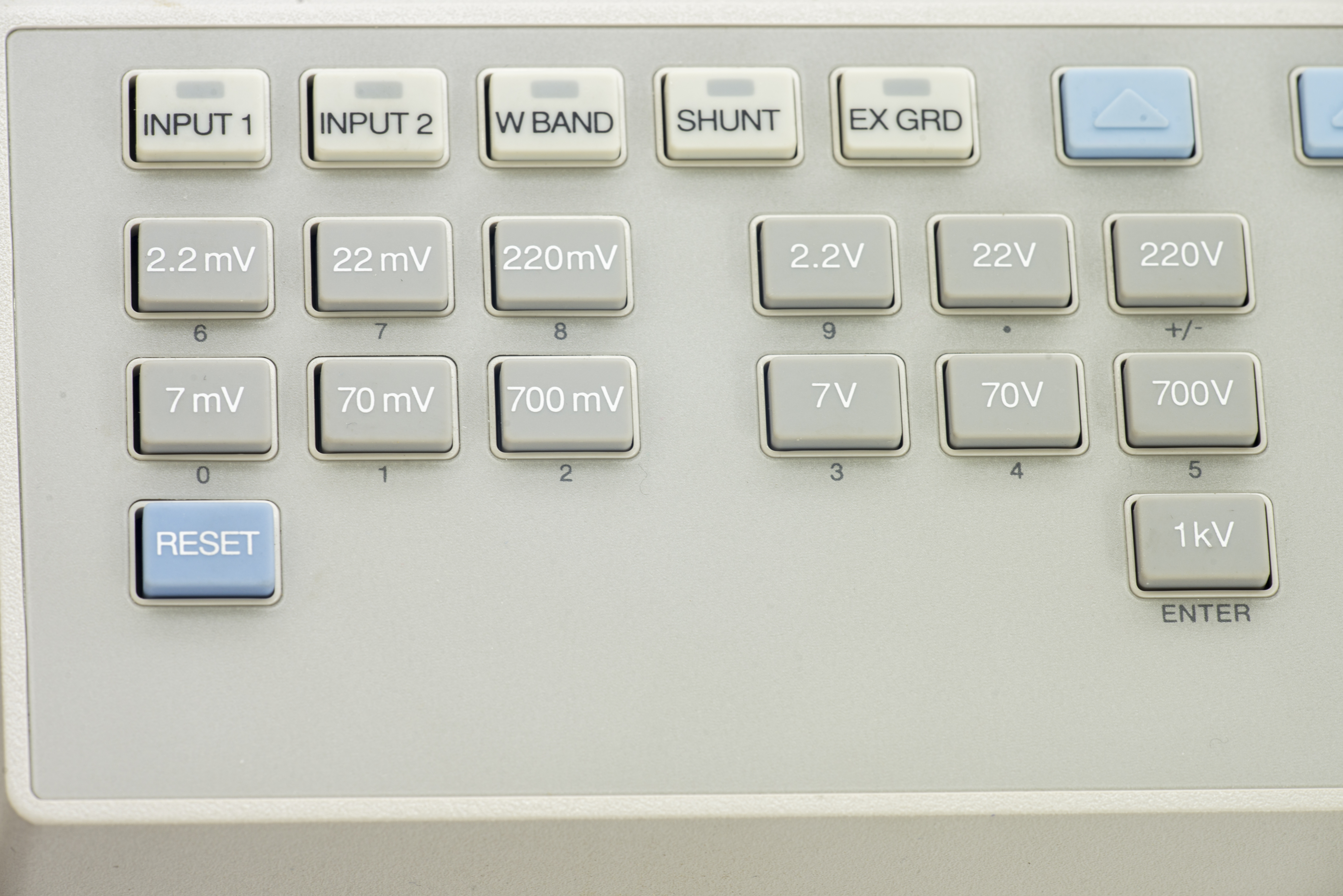 |
Image 2-4: Front panel inputs, face and keypad
A variety of input connections allows versatile use that best suits specific application and equipment interfaces. There are four sets of input terminals on the 5790A, two 50Ω Type “N” connectors and two sets of five-way binding posts. One 50Ω Type “N” and one set of binding posts is dedicated to the AC measurement and transfer modes. Unlike some older standards like Wavetek 4920/4920M AC or DC voltages can be applied to either input connection, allowing you to perform automated AC-DC transfer measurements.
The second Type “N” input connection supports only the optional wideband mode, and is unconnected internally on standard 5790A. SHUNT binding posts are for Fluke A40 Series current shunt connection.
5790A does not have rear connectors.
Here we can also see what is the problem with the instrument. With nothing connected to the input terminals, we get overload condition with beeping alarm.

Image 5: Diagnostic run results
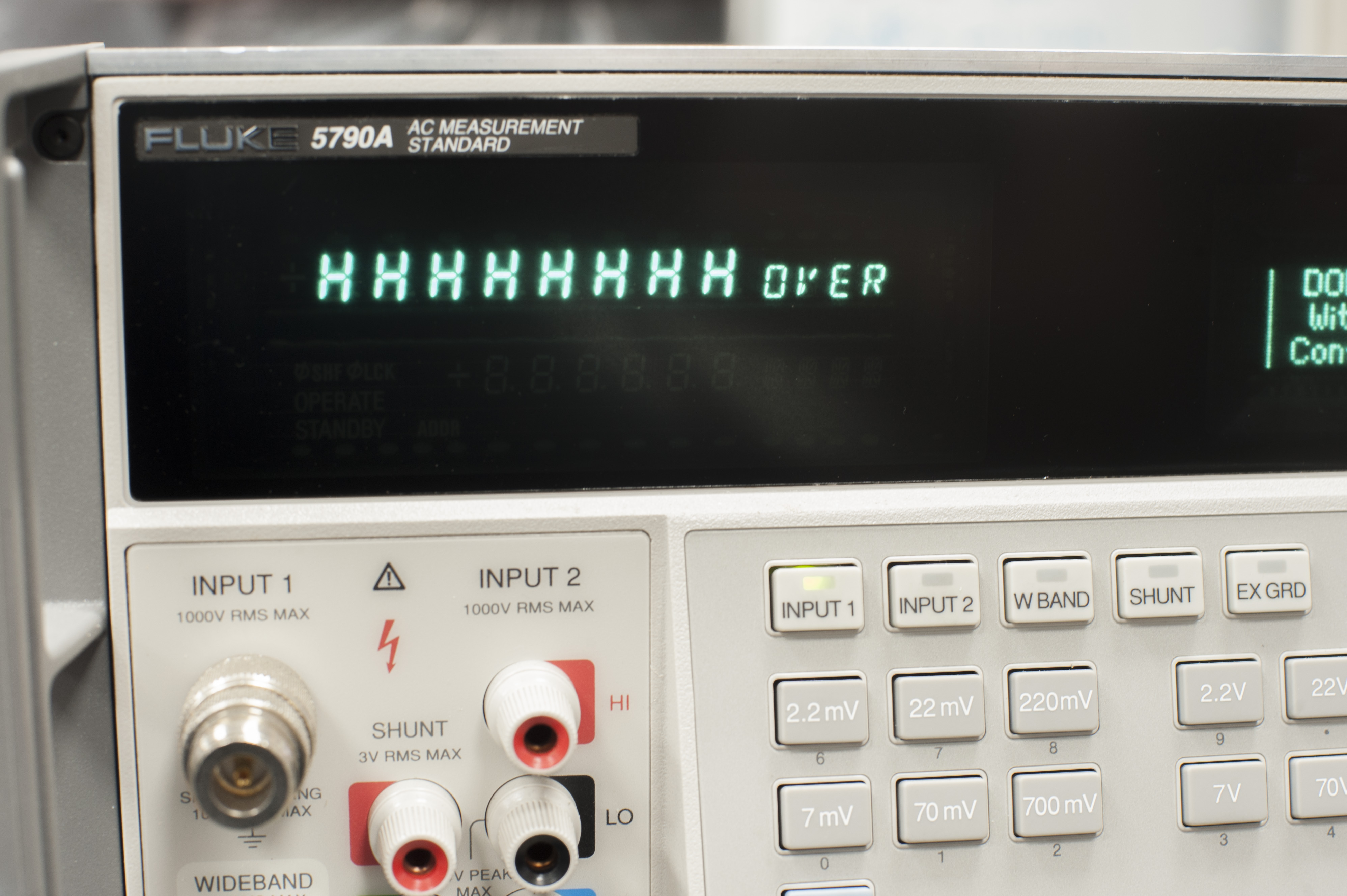
Image 6: Running condition with no signal applied
After removing external top metal shield we can see separate shielded sections for in-guard precision circuitry and out-guard section on the right with mains custom transformer and digital processor board and power supply assembly. Also there two 92mm size cooling fans.
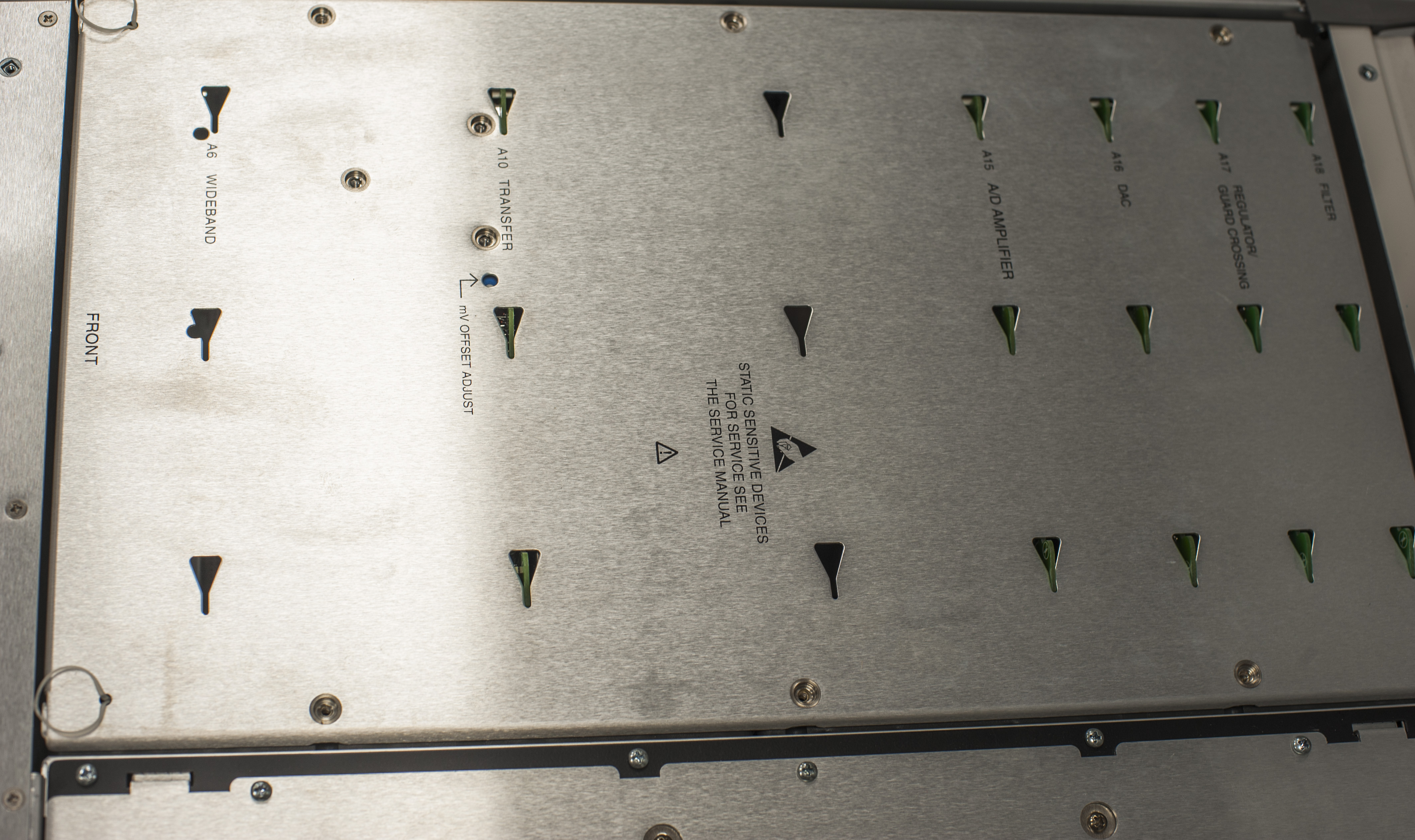
Image 7: Top cover removed, revealing shielded inner boxes
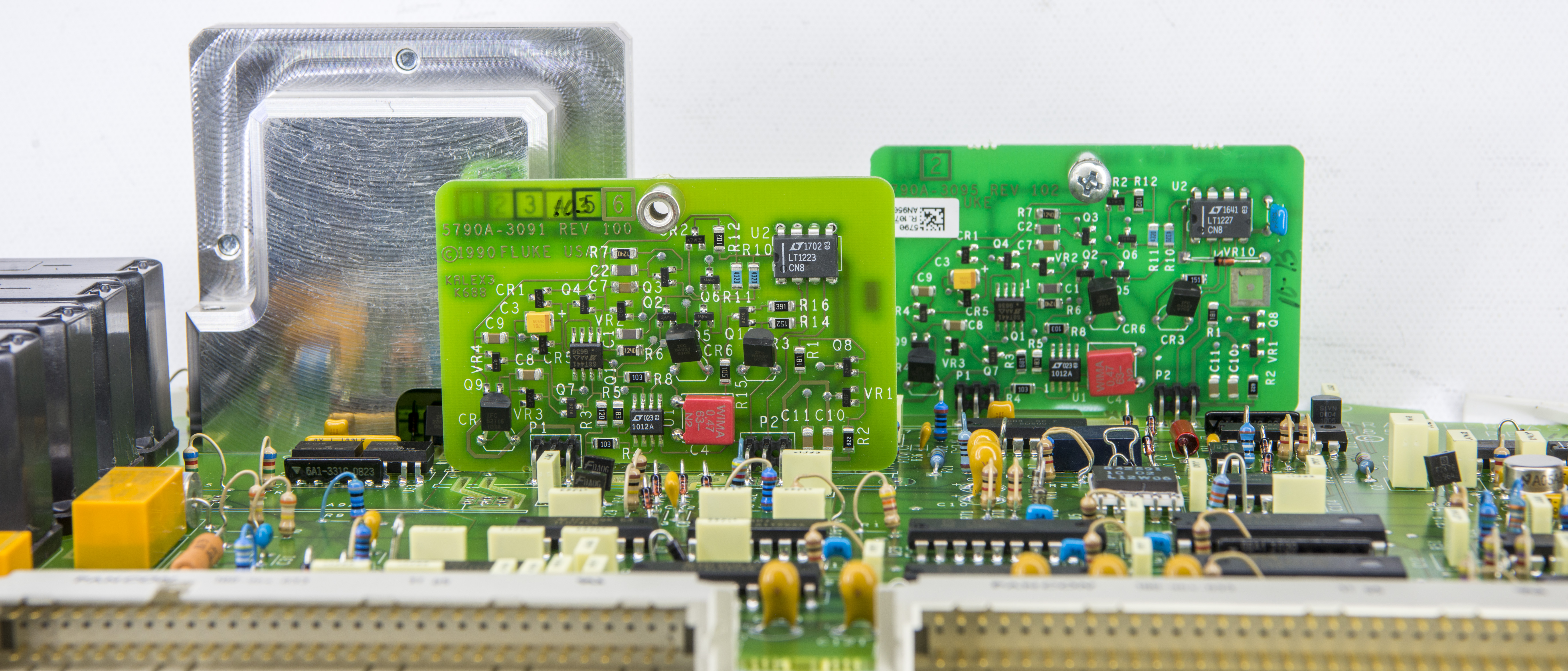
Inguard section have a lot of free space. and essentially have only 5 boards (6 with Wideband PCBA). We will take a look on each of the boards in better detail in next section.
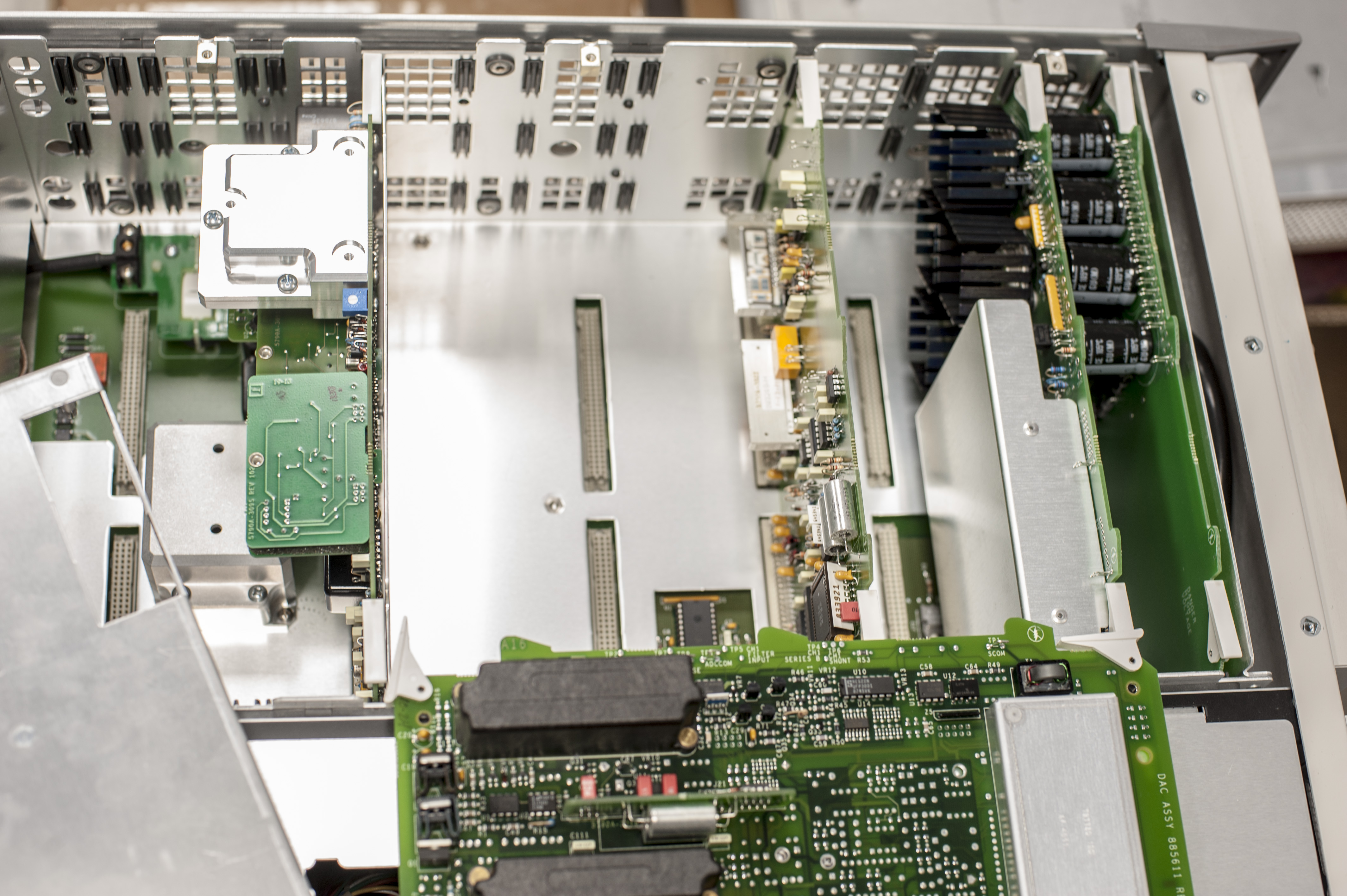
Image 8: In-guard modules and assembly cards
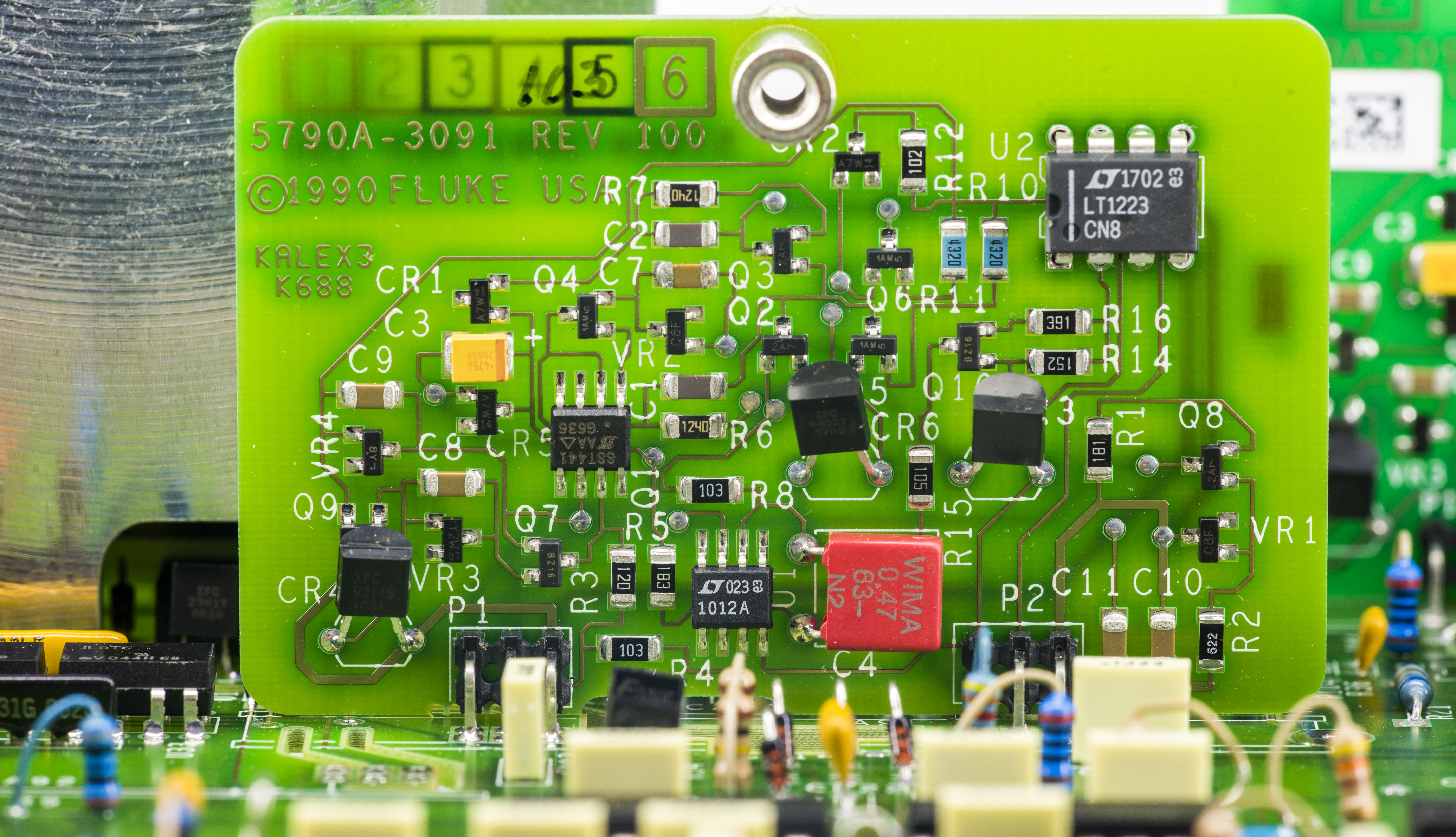
A16 PCBA – DAC + main DC Reference

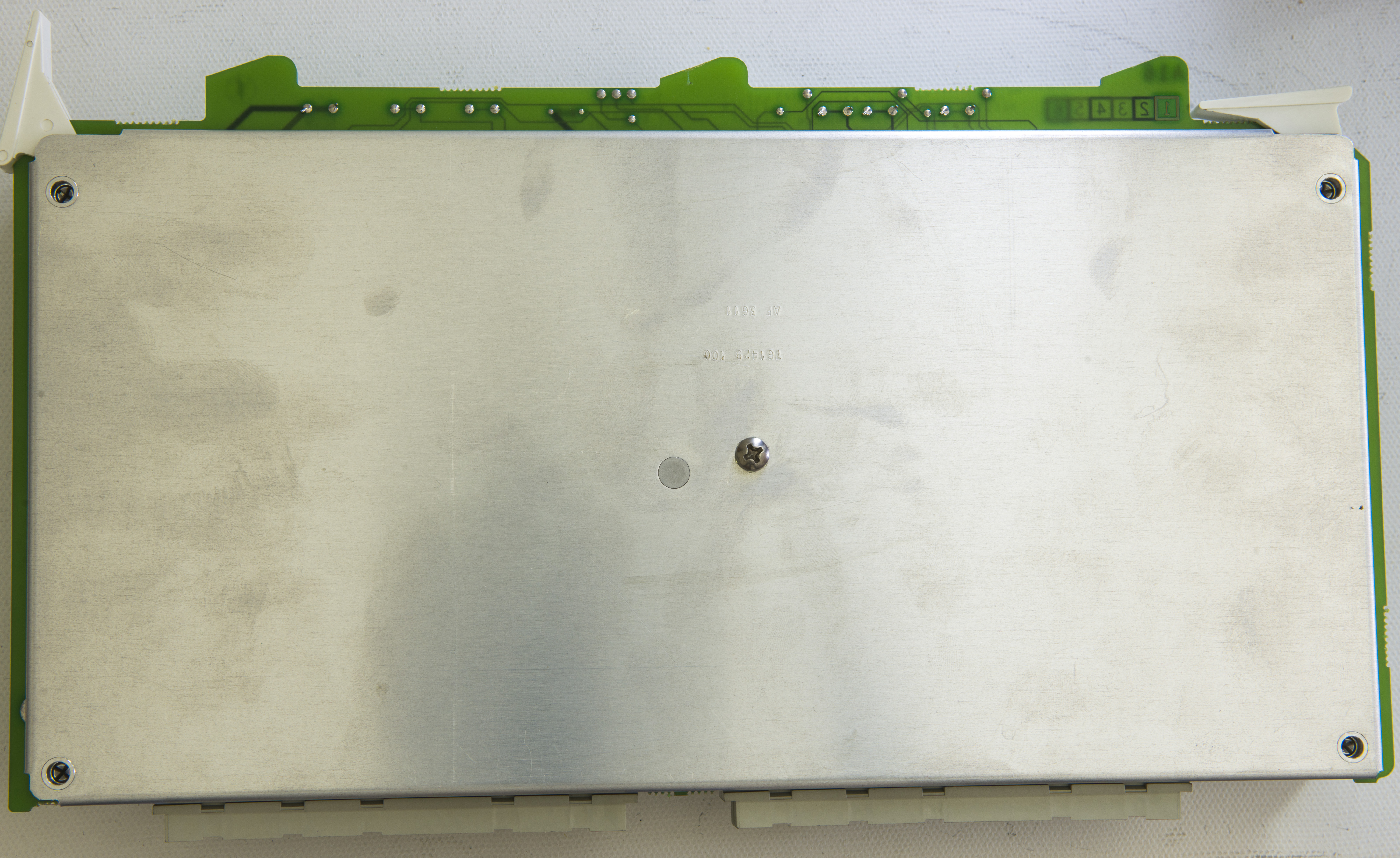
Image 9-10: 5790A A16 DAC reference board top and bottom
“Magical” reference, based on two Linear LTFLU ref-amps. Design of this high-performance non-heated buried zener was covered in better detail in this article.

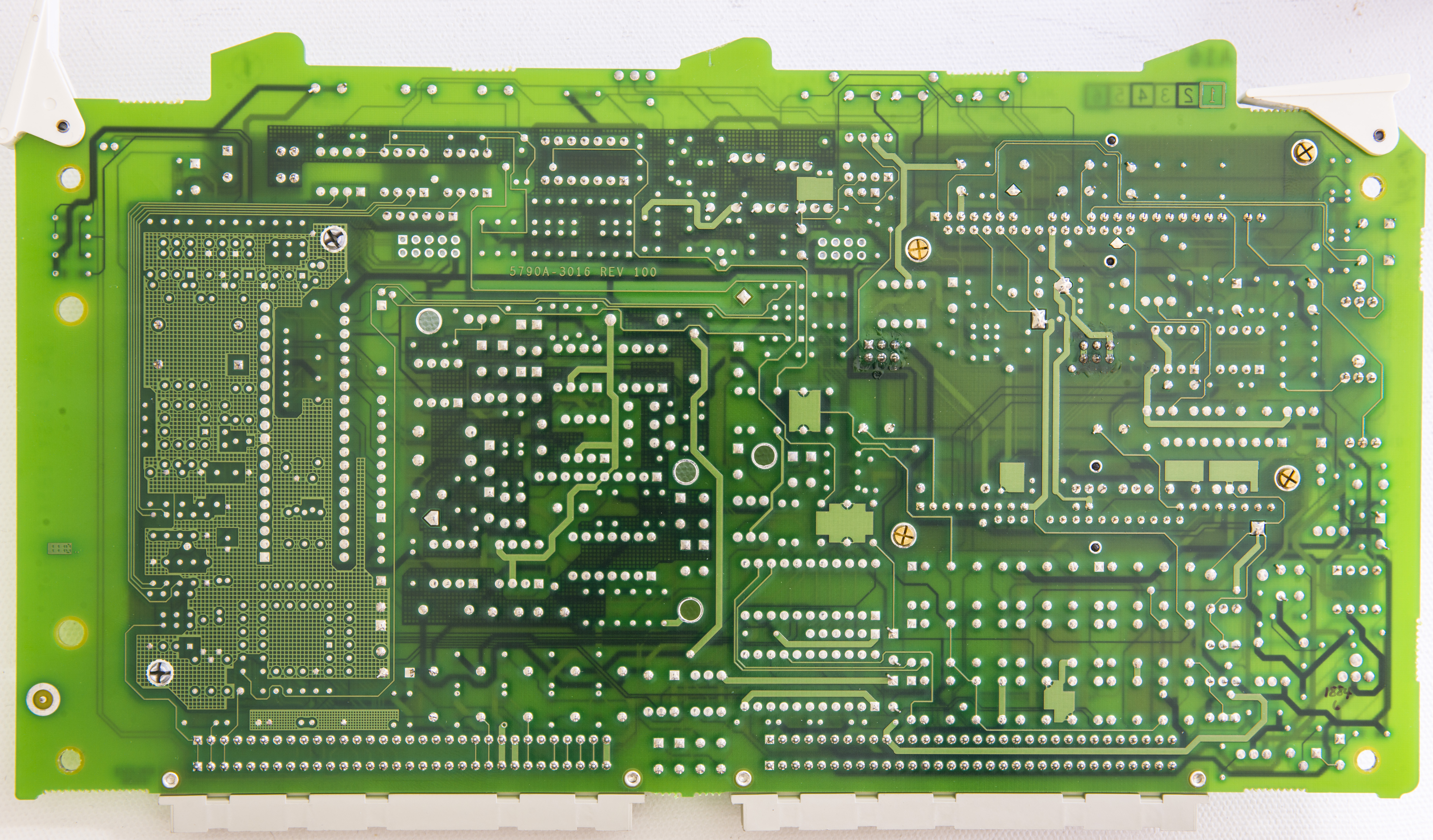
Image 11-12: Fluke 5790A A16 DAC with inner shields
This board is very same design of the A11 PCBA from 5720A, with removed null-meter ADC logic.
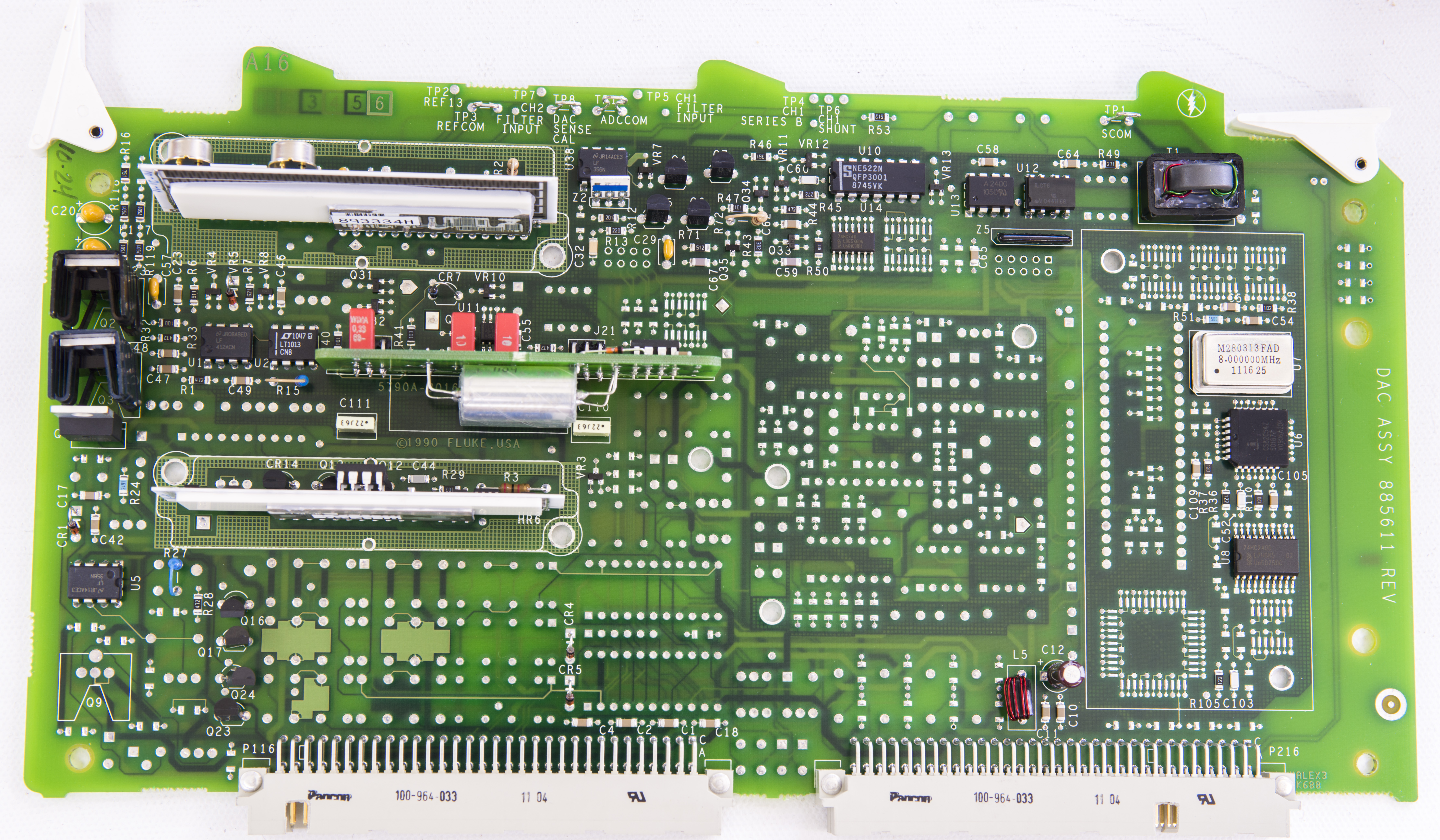
Image 13: A16 DAC reference board with shields removed
ADC circuitry was moved to the separate assembly in 5790A, so there is no need to have ADC on reference board anymore. Reusing same PCB design save time and design effort, as original design from 5700A was already validated and tested for high performance specifications.
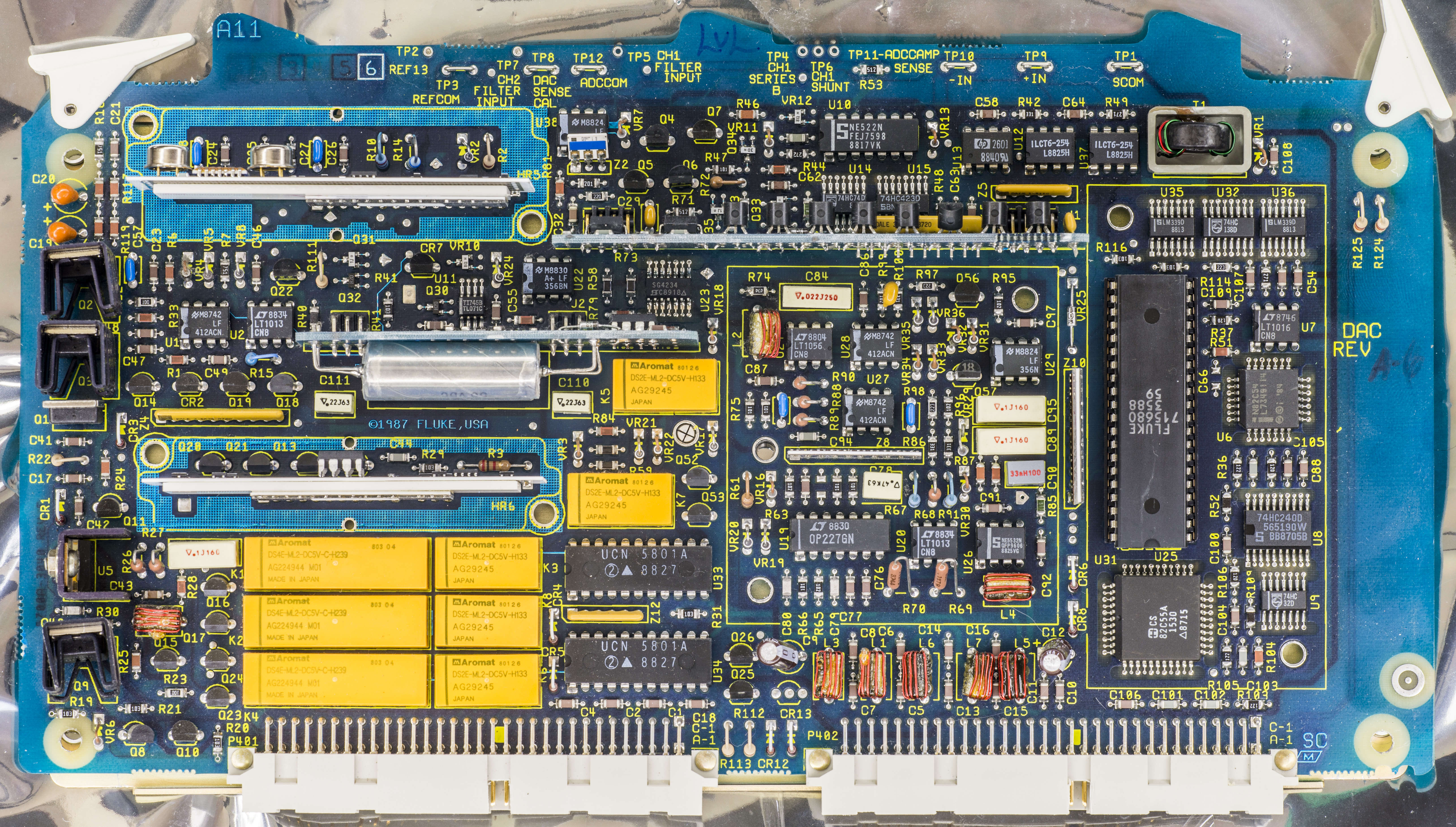
Image 14: Counterpart Fluke 5700A A11 DAC reference board for comparison
As can see from date-codes on the reference cans, this board is just 7 years old, with selected LTFLU-1ACH chips, manufactured in 5th week 2011 and 39th week 2010. Refamp resistors to set zener current and scale output voltage are implemented in custom Fluke film resistor network P/N 759522.
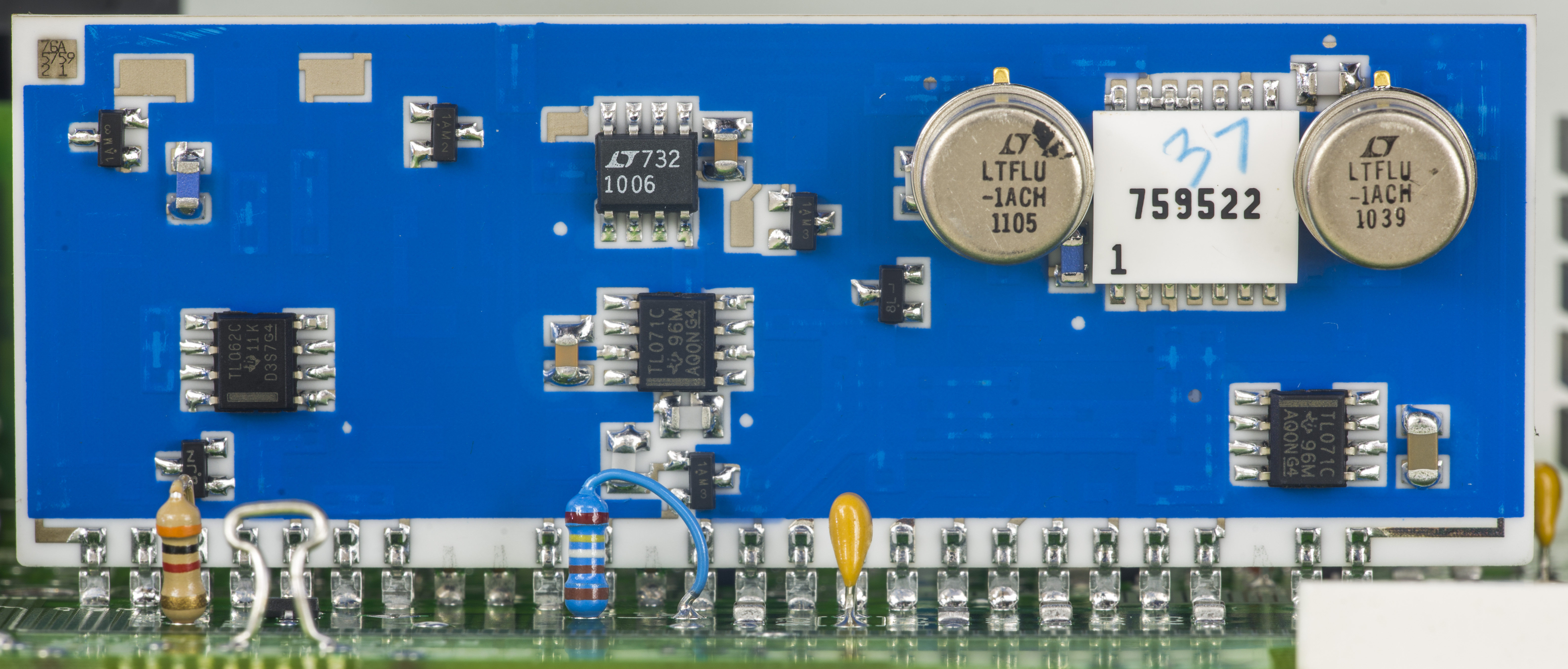
Image 15: Fluke 5790A DC +13V dual LTFLU-1ACH reference
Whole ceramic hybrid assembly kept at constant +62°C by using heater resistors on the rear side of the main carrier board. Additional precision resistor network P/N 893334H is thermally bonded to the back of the ceramic assembly. Whole module is covered by plastic cover to avoid air drafts and maintain constant air bath temperature inside.
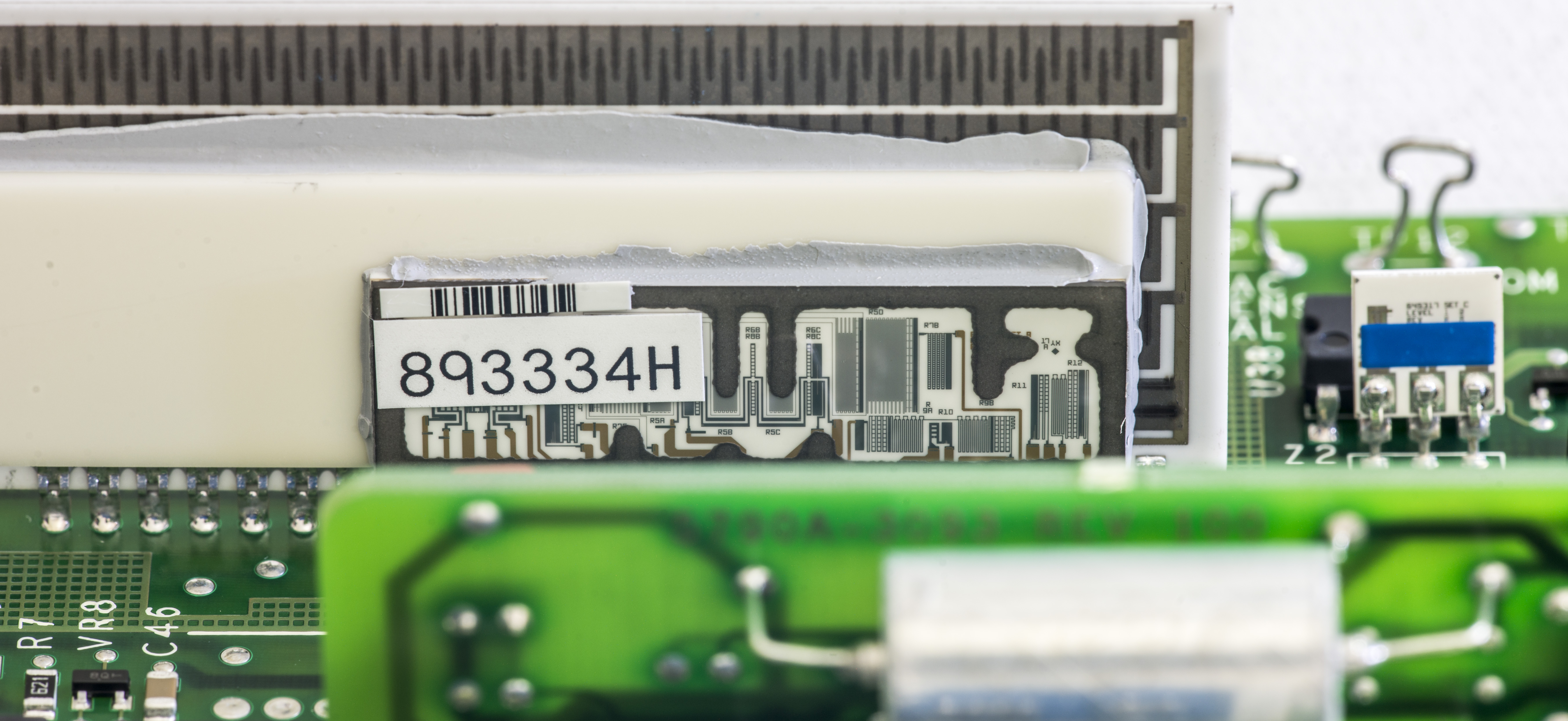
Image 16: Gain and scale resistor hybrid network and backside of the heater SIP
This is crucial for high precision voltage output, as even tiny temperature gradients can cause thermocouple offsets much higher than LSB of the DAC output.
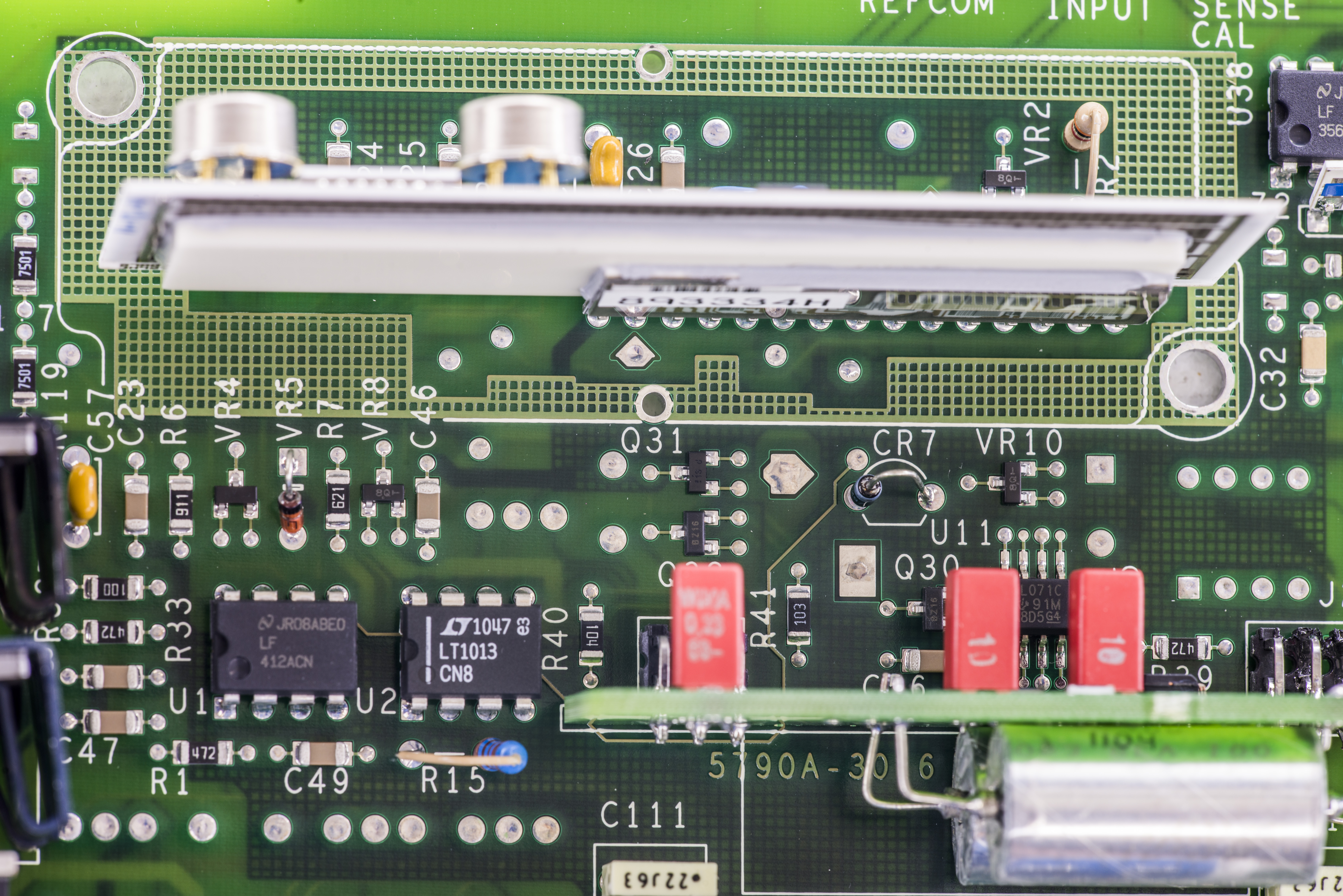
Image 17: Top view on reference SIP
Fluke used PWM-controlled method to generate adjustable voltages. There are also few auxiliary support circuits on-board, such as sense-current cancellation block, linearity tune control, negative offset control. Block diagram below on Image 4 can help to understand overall function of circuitry on A11 DAC PCBA.
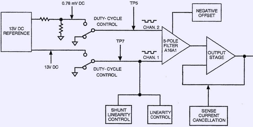
Image 18: DAC block diagram, same as 5700A calibrator.
Output DC voltage is generated by 5-pole discrete filter, which has two precision square waves of different amplitude as the input. First input channel of the filter is CH1, and it’s amplitude is from 0V to reference voltage, which is around +13 VDC. This is coarse adjustment channel. Second CH2 channel is operated similar way but goes up only to attenuated reference voltage at +0.78 mVDC. This is fine tune adjustment channel. Filter is designed as LPF with bandwidth 30 Hz, and input square wave frequency is 190 Hz. So the output is clean and filtered DC voltage, derived from controlled PWM CH1 + CH2.
Filter output does not have capability to drive large currents, so output stage on separate ceramic hybrid takes filter output and provide driving capability for DAC output. Hence after all, circuit output voltage can be predicted and calculated by simple formula:
VOUT = DutyCH1 × VREF13V + DutyCH2 × VREF0.00078V
Here’s realtime example to try some values to generate precise 10V:
Use of this combined PWM scheme allows us to have efficient way to generate arbitrary voltage levels without use of very expensive resistor networks and expensive complex multi-bit DAC ICs. PWM duty cycle resolution of PWM generator used in Fluke calibrator is 0.0024%, which provides resolution of CH1 = 309 µV/bit and CH2 = 18.5nV/bit. PWM signal also electrically isolated by optocouplers.

Image 19: DC chopper output amplifier
Output of the DAC reference is buffered by LTC1052-based chopper amplifier on separate ceramic hybrid HR06 assembly. It’s same solution used on 57xx calibrators. Chopper amp has own resistor network on the back, Fluke P/N 761411H. Handwritten datecode reveals manufacturing/testing date 24 October 2011.
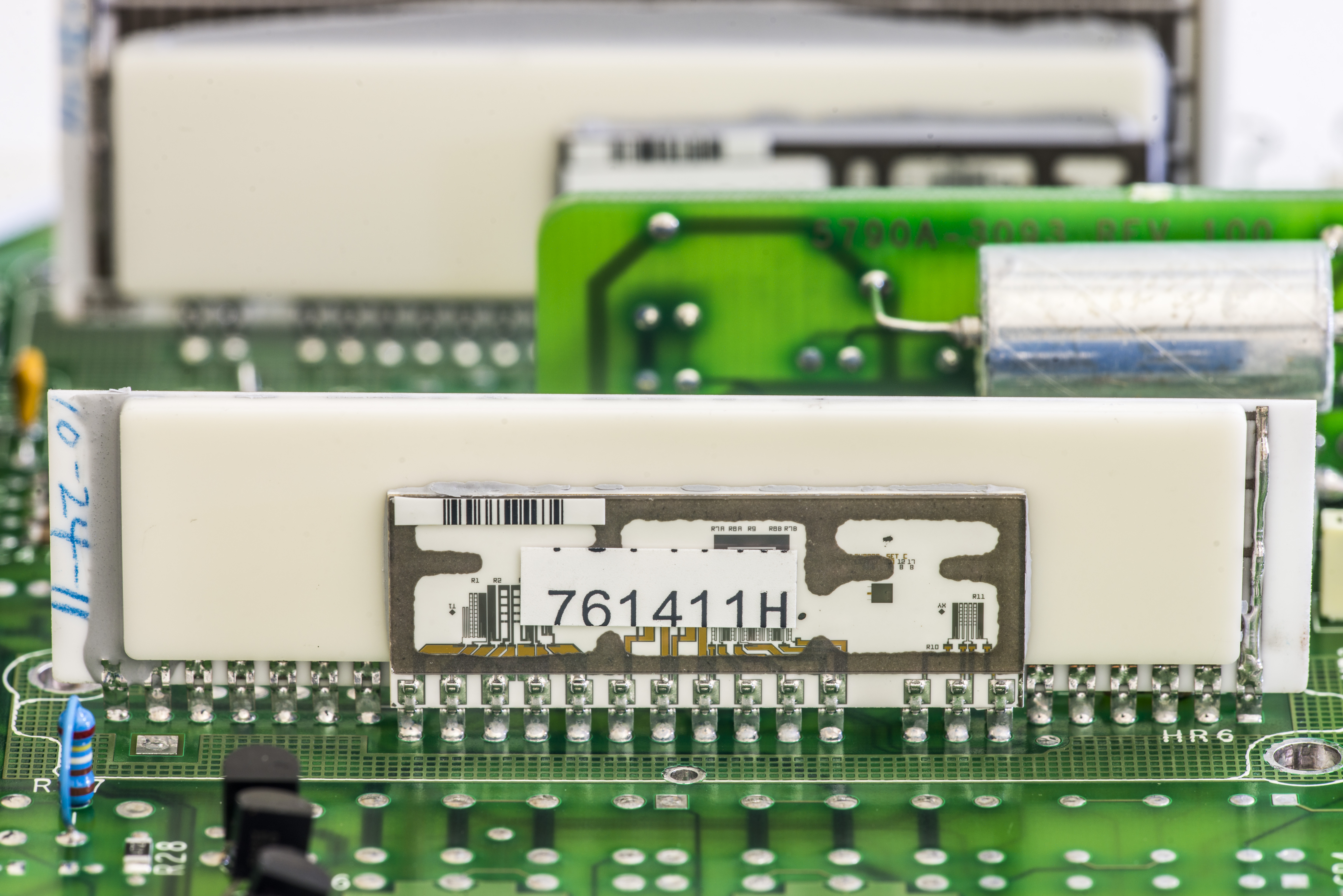
Image 20: Fluke 5790A chopper hybrid resistor network
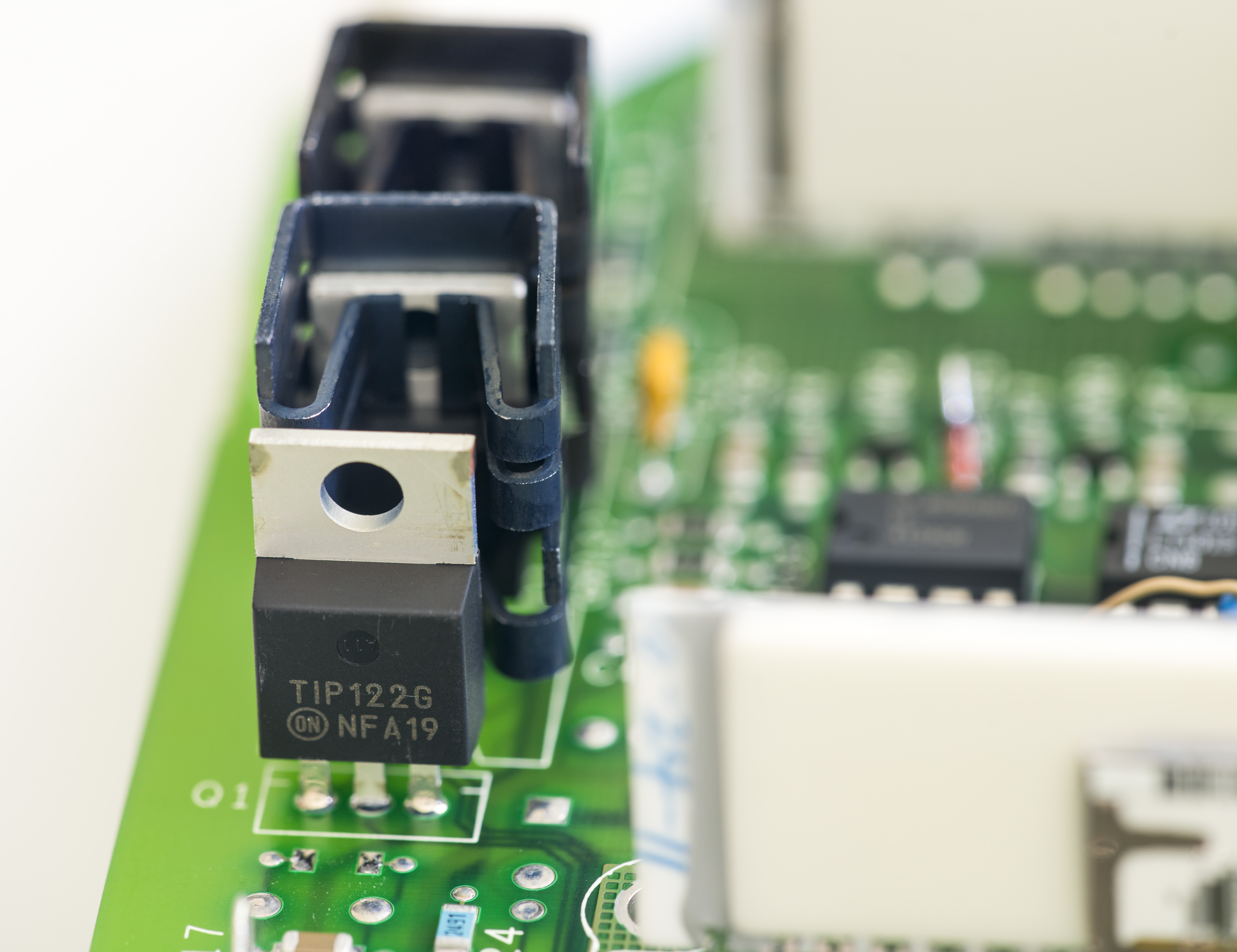
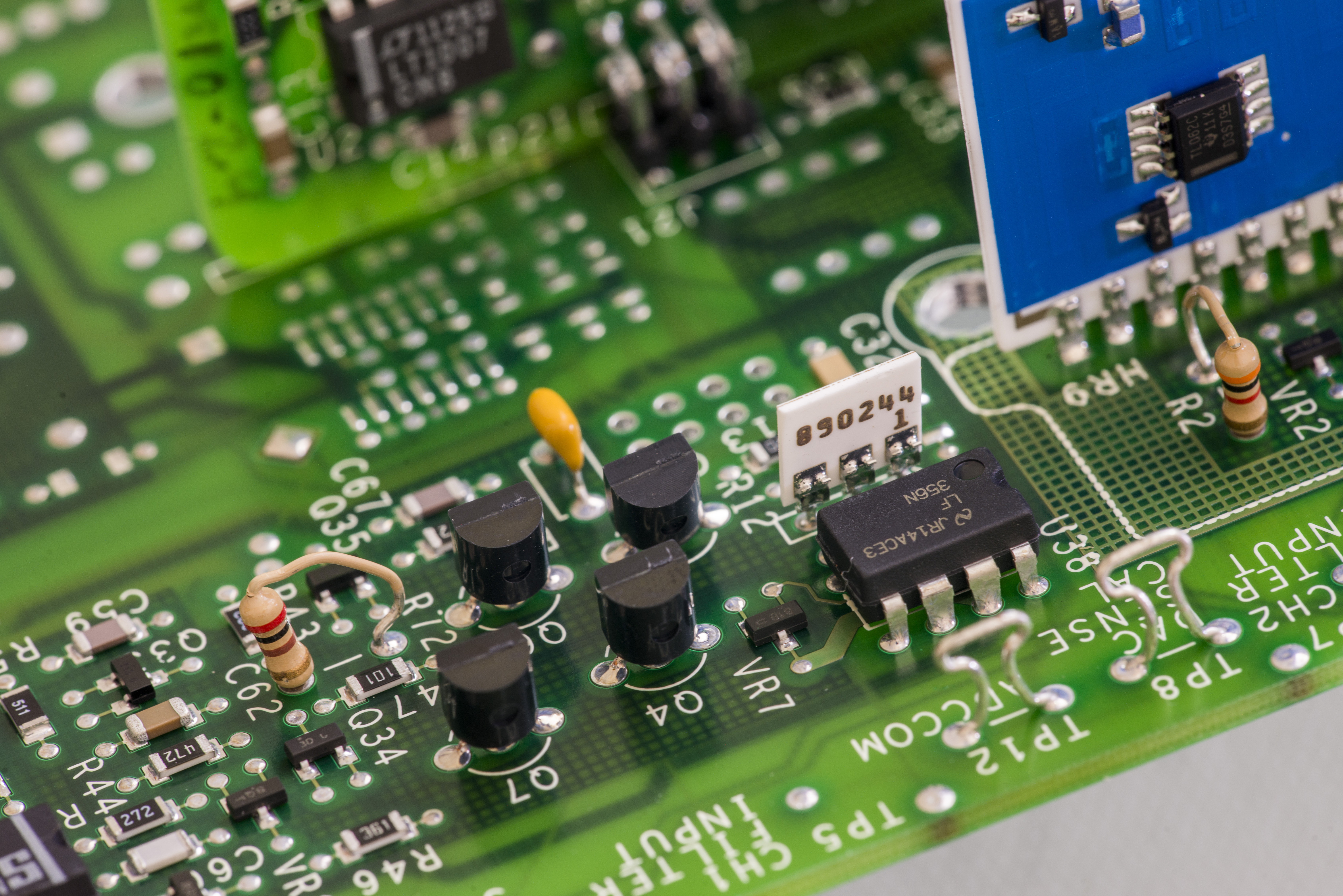
Image 21-22: Fluke 5790A A16 DAC parts and circuits
Heaters are driven by onboard power sources, with few power transistors in TO-220 package.

Image 23: Fluke 5790A A16 DAC digital bus interface
DAC is controlled by Intersil CS82C54 interval timer, clocked by 8 MHz XO nearby. This timer/counter have up to 3 channels.
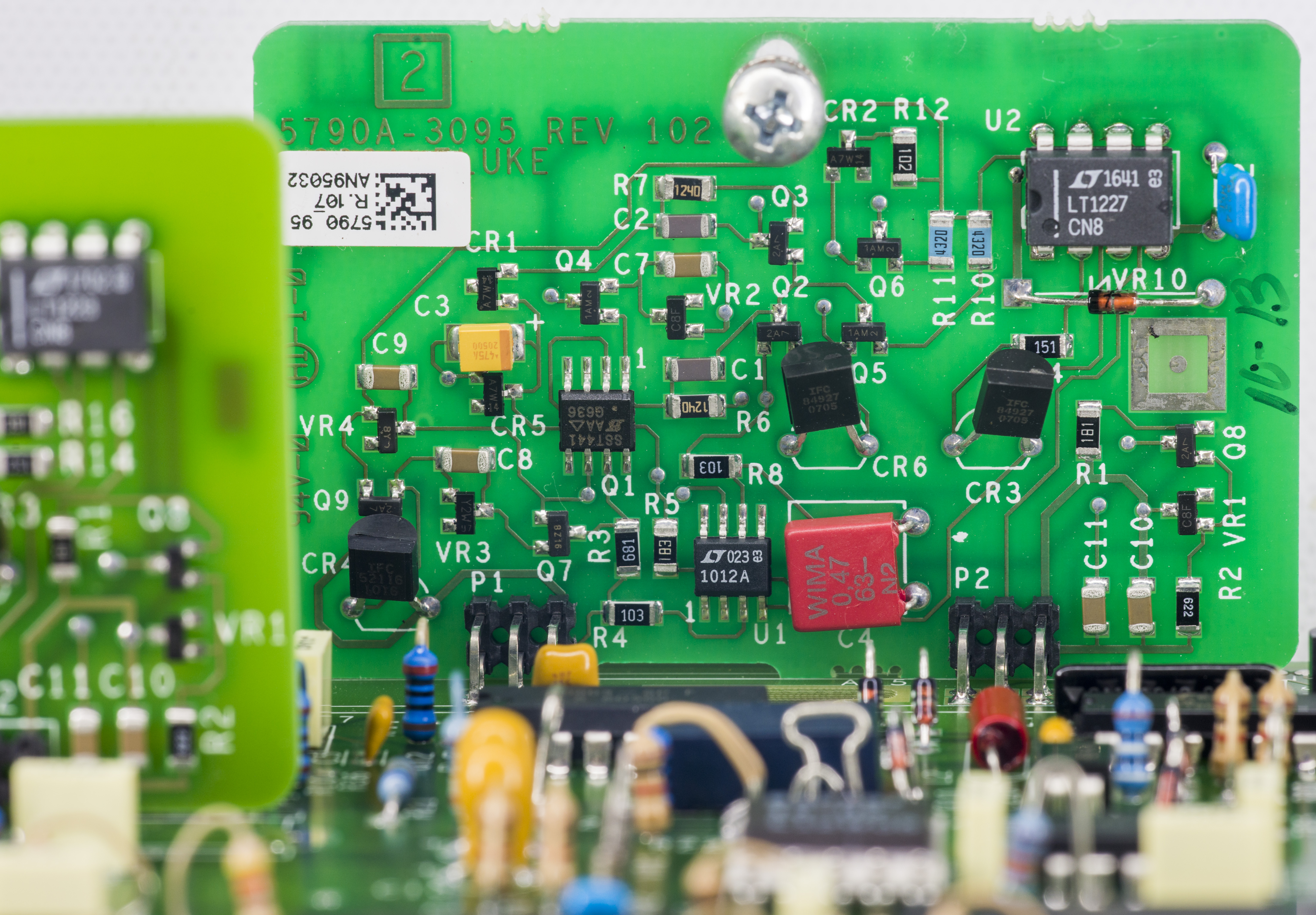
A17 PCBA – Inguard crossing and regulated supply
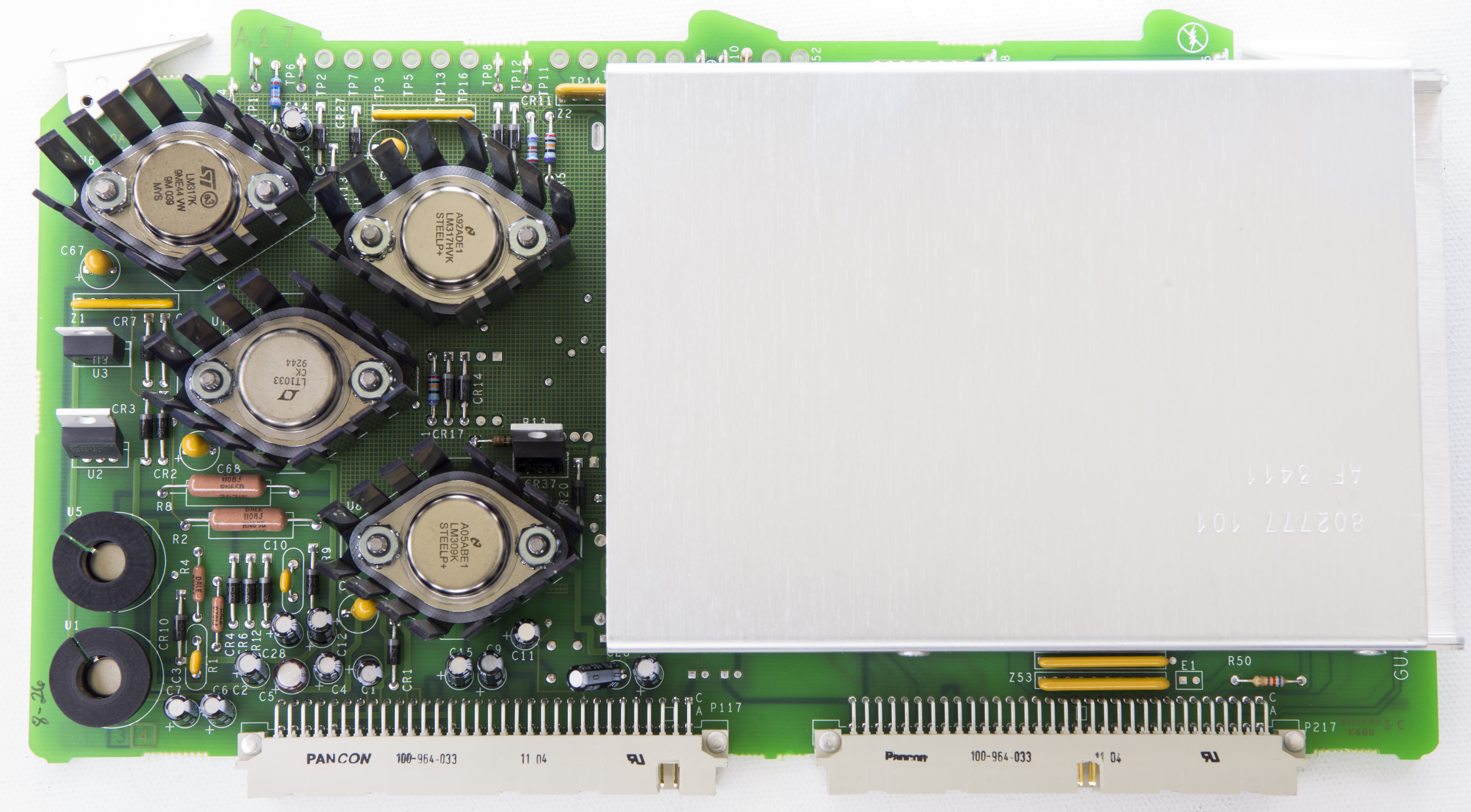
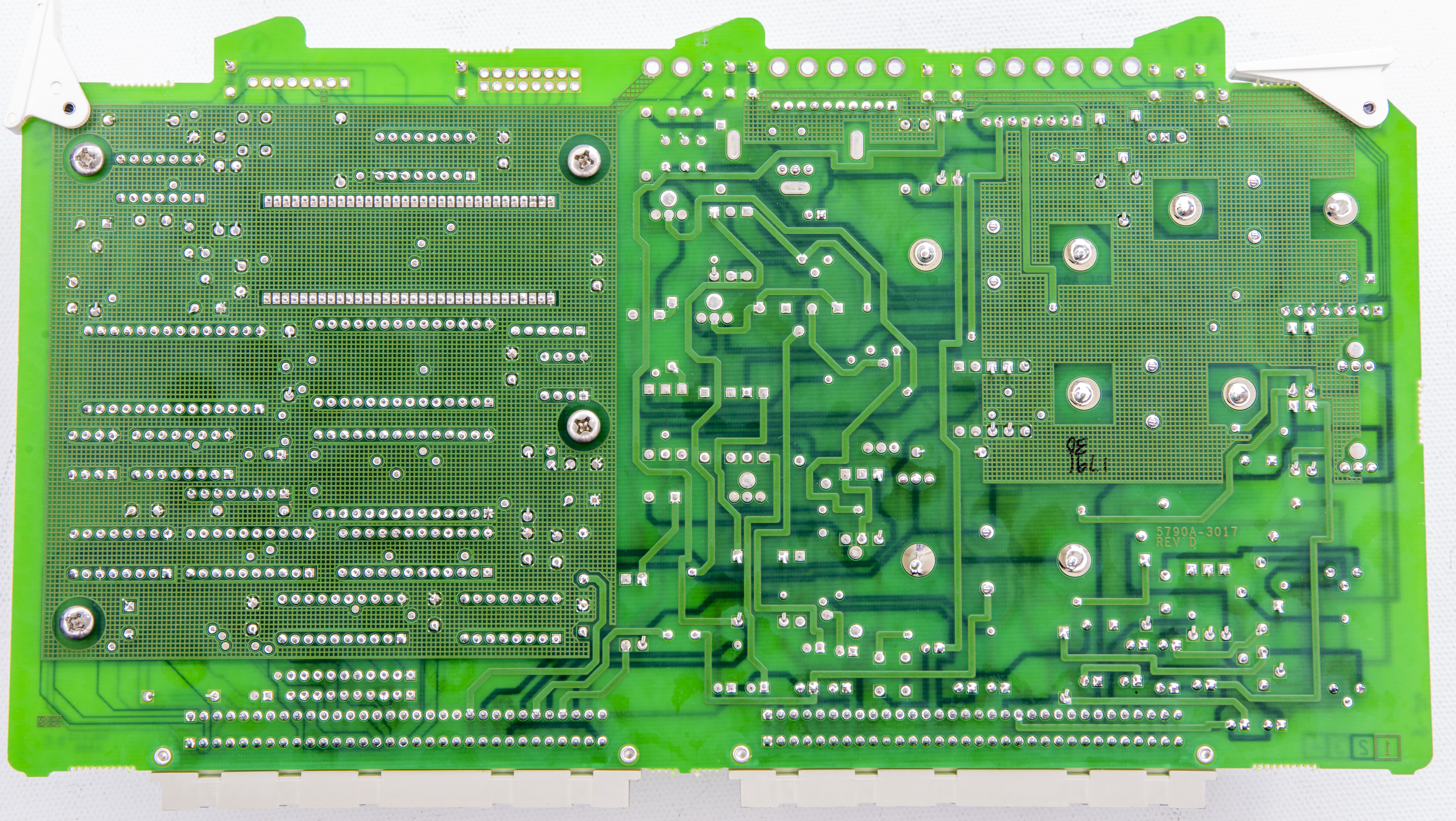
Image 24-25: Fluke 5790A A17 regulator and interface board
This board is also nearly same as one from 5700A.
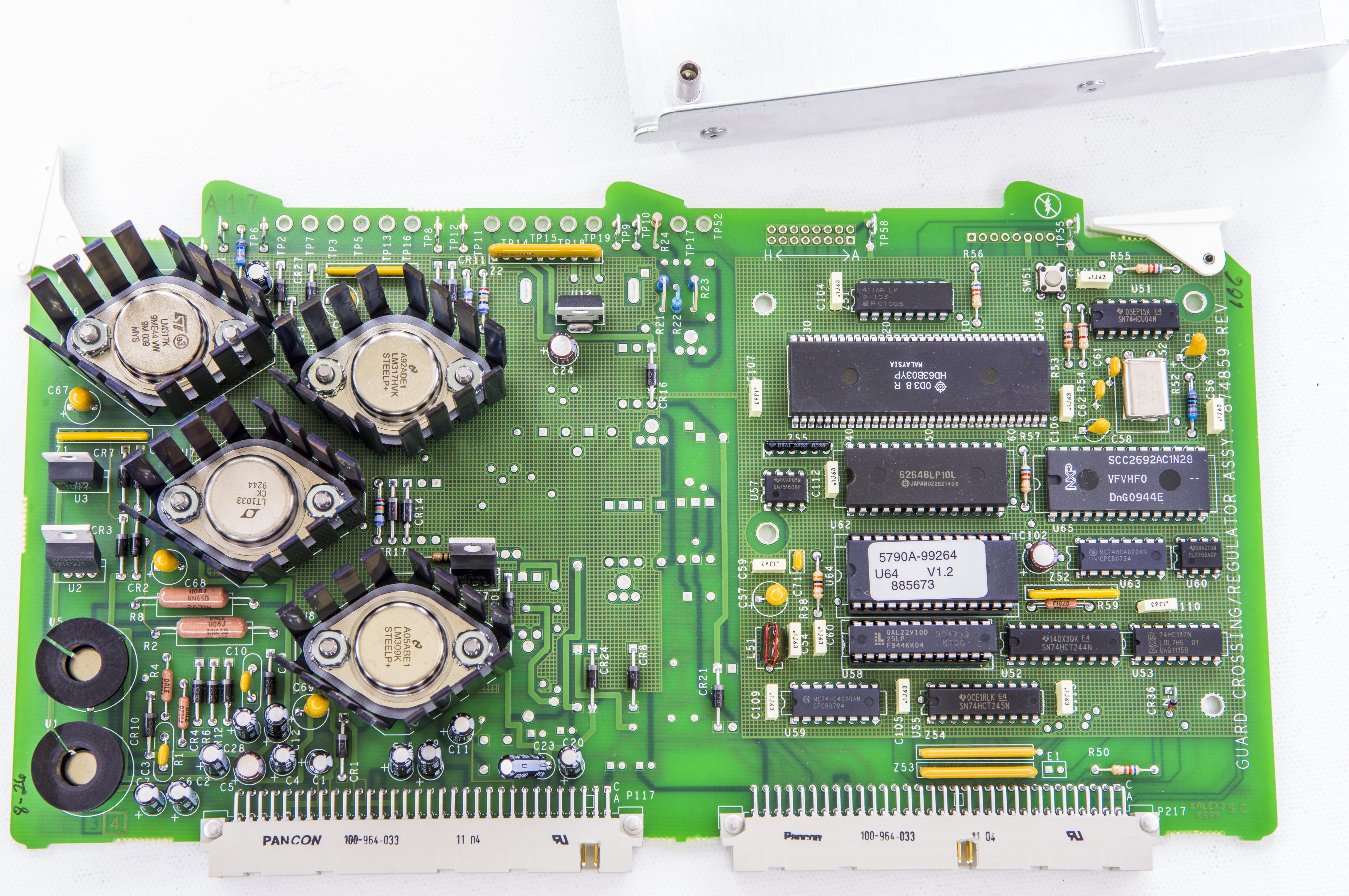
Image 26: Fluke 5790A A17 with shields removed
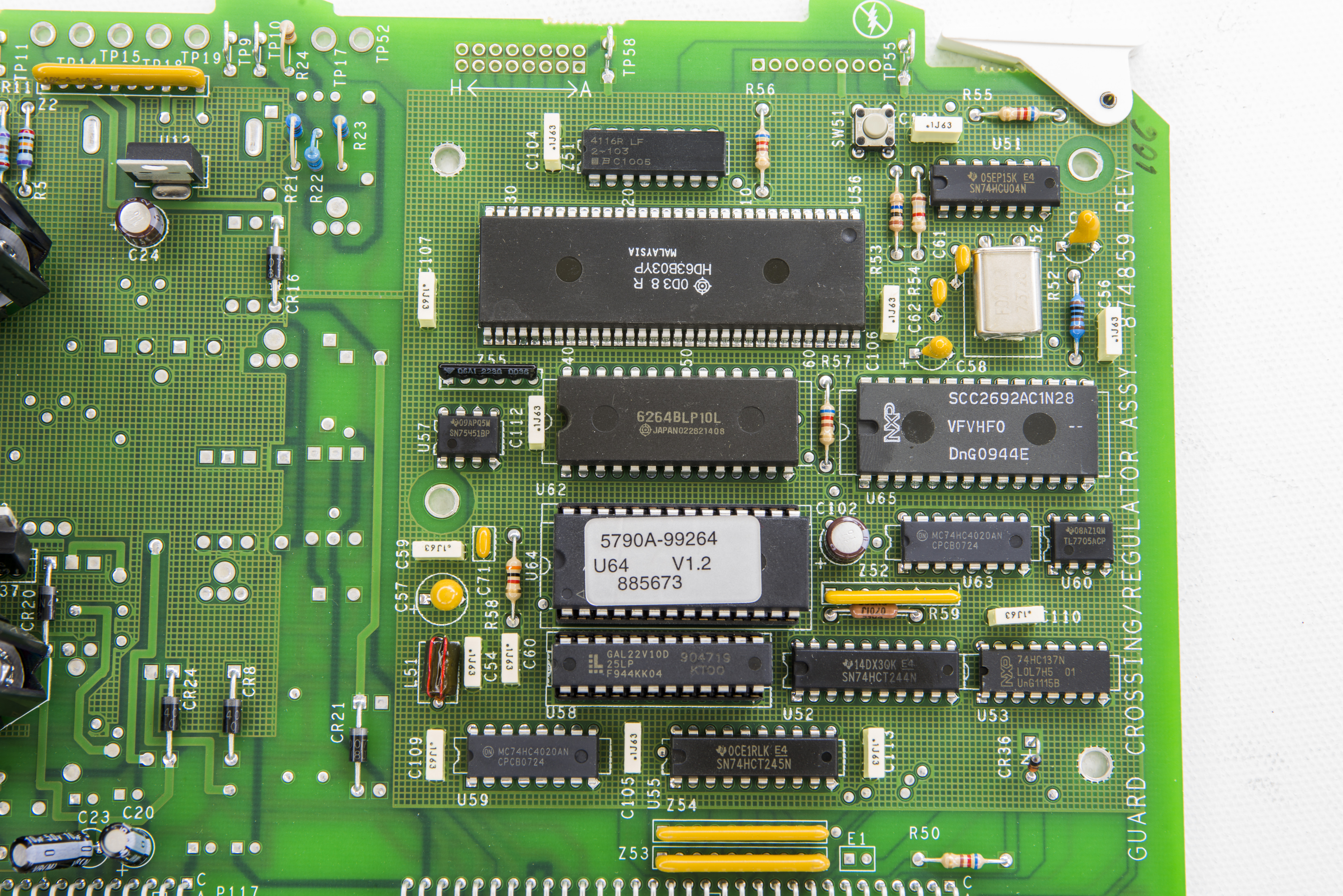
Image 27: Fluke 5790A A17 in-guard MCU, firmware ROM, SRAM and interfacing logic
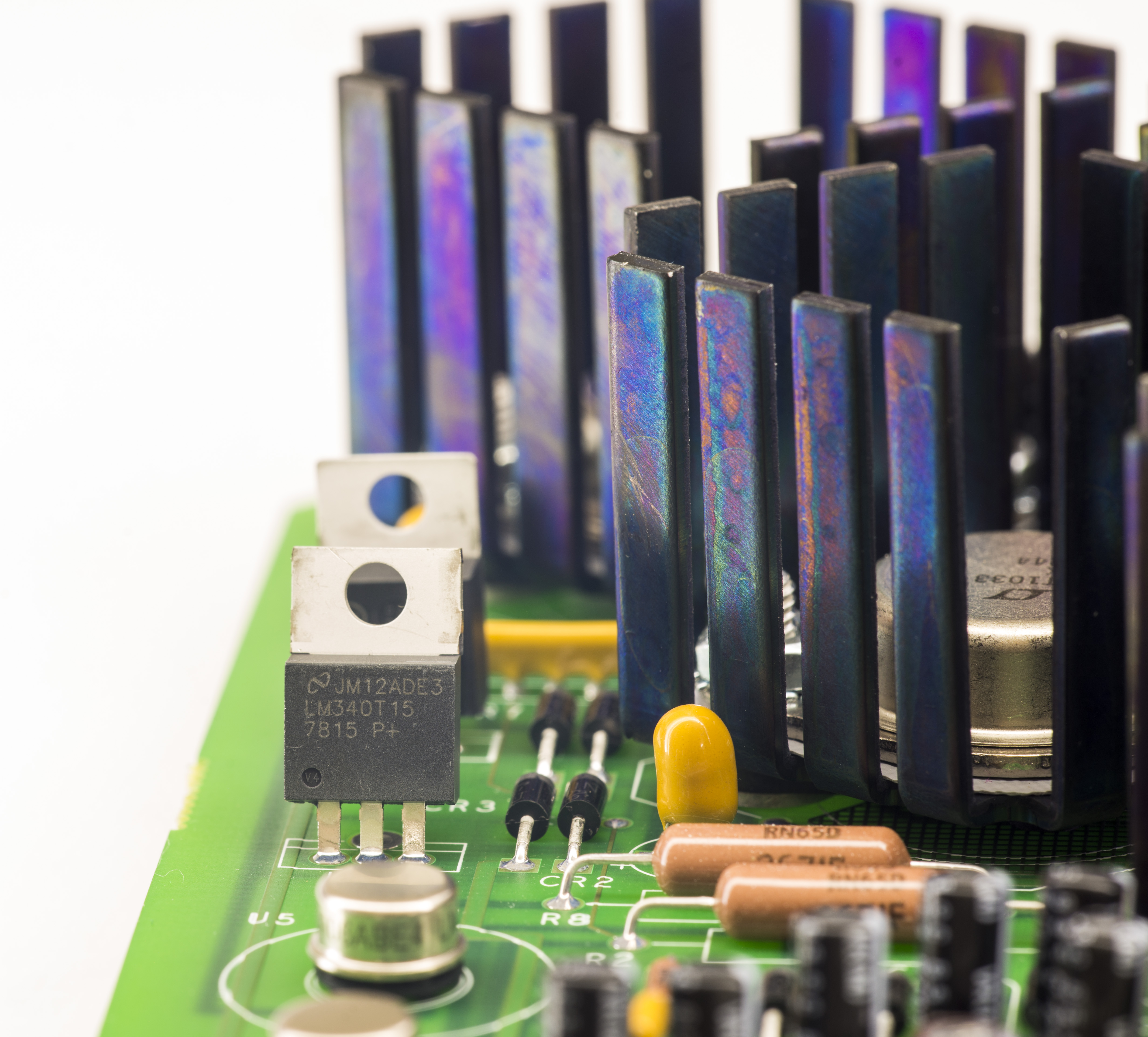

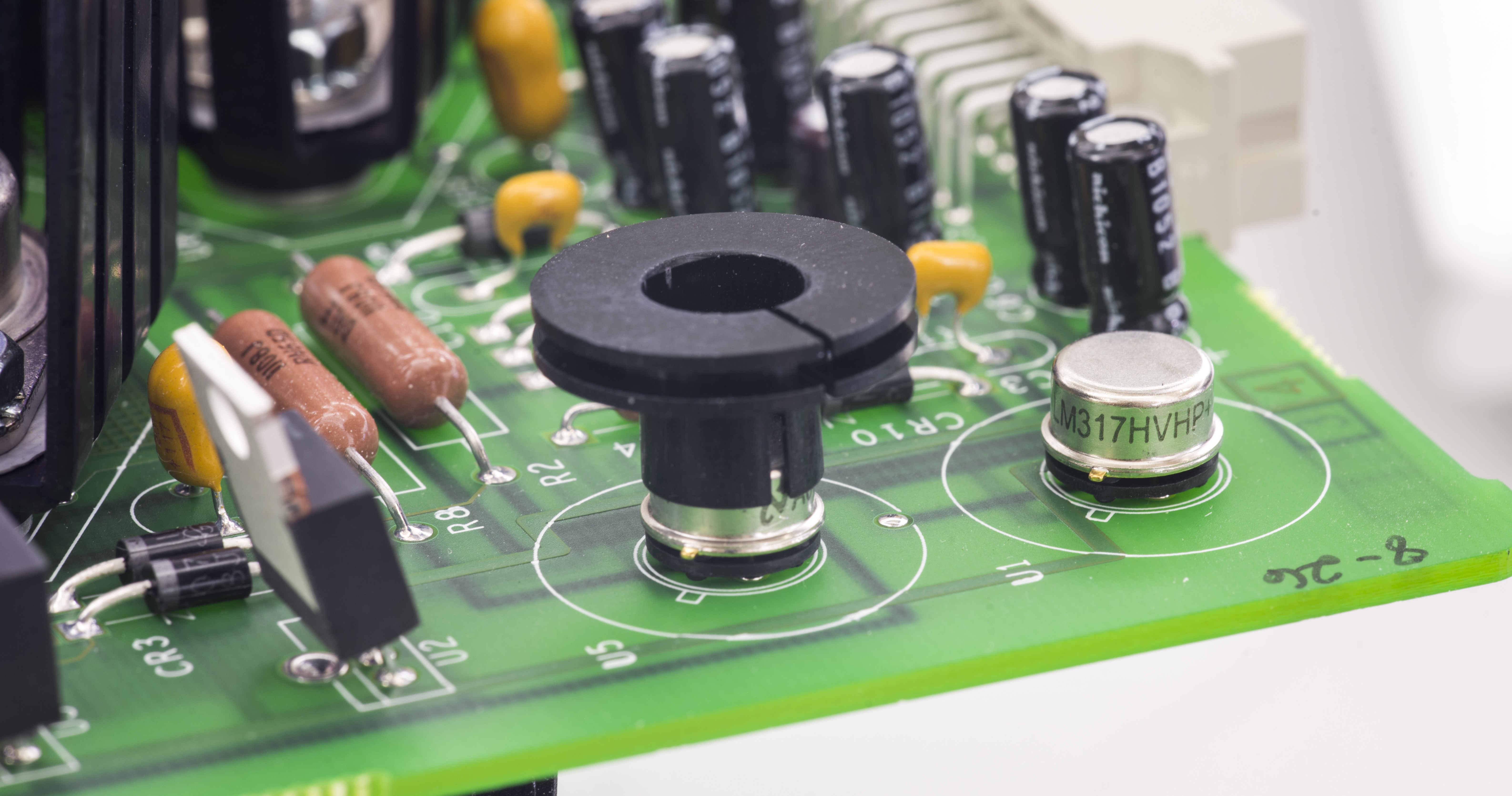
Image 28-30: Fluke 5790A A17 components and regulators
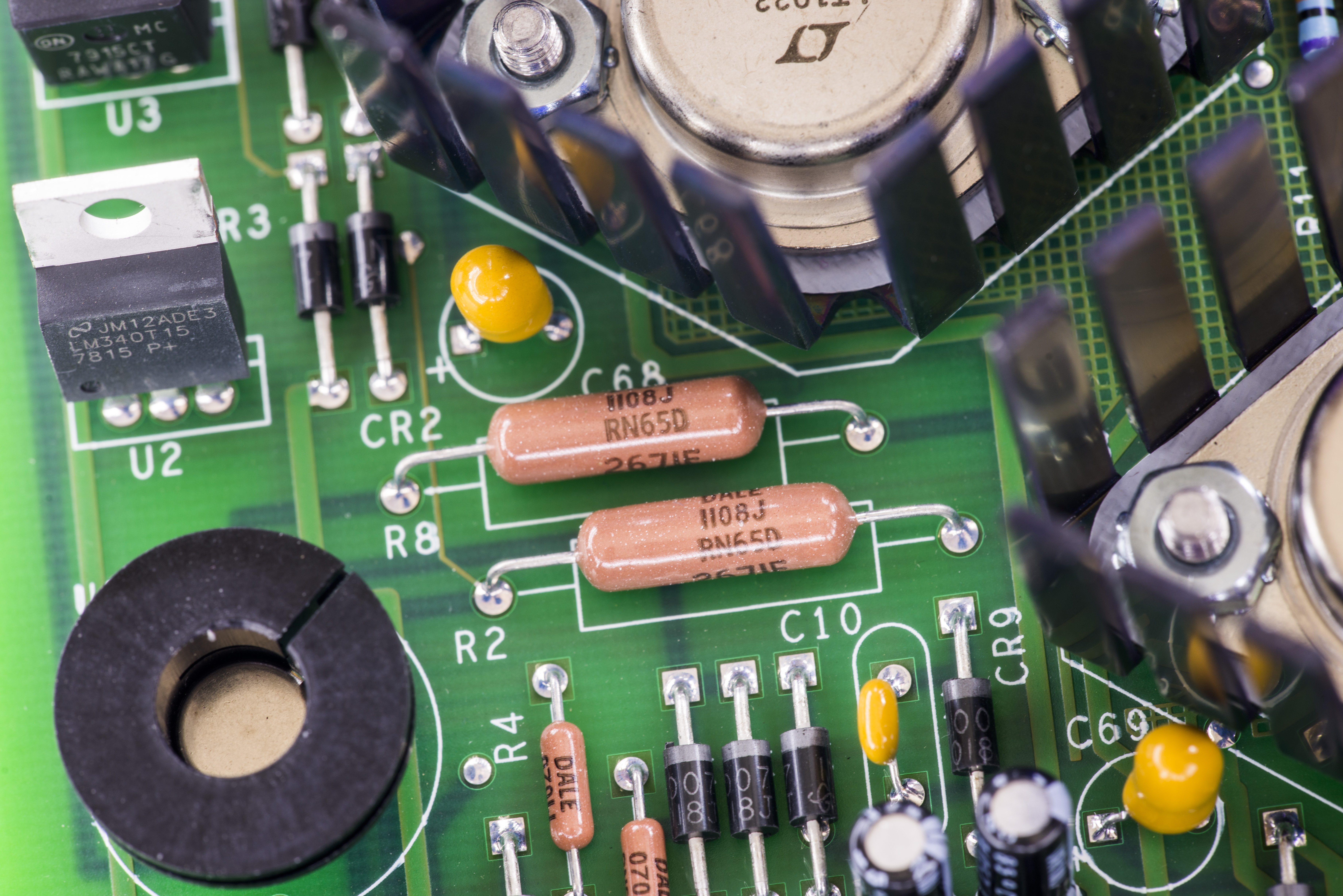
Image 31: High-power resistors on A17
A18 PCBA – Unregulated power supplies
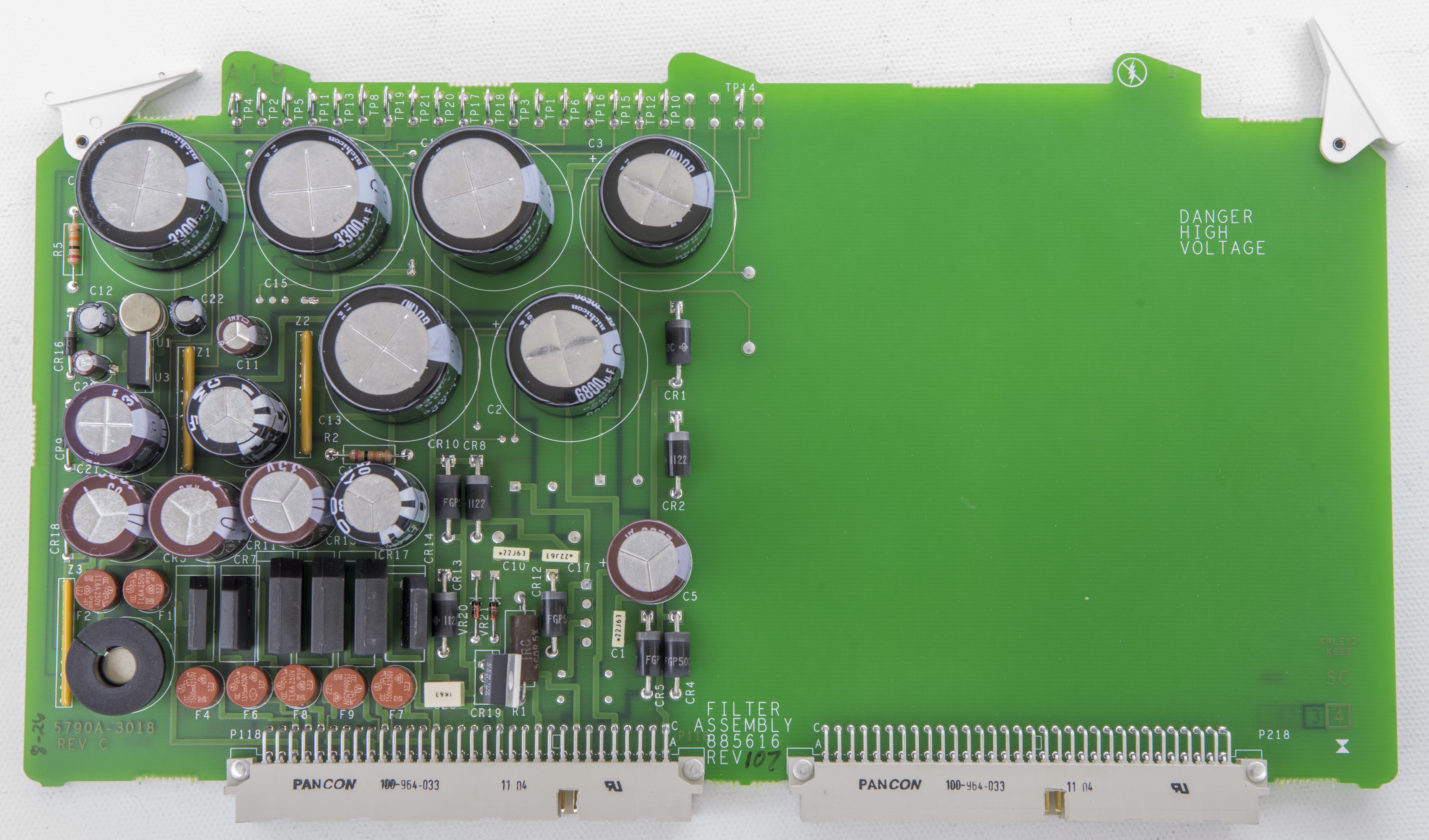
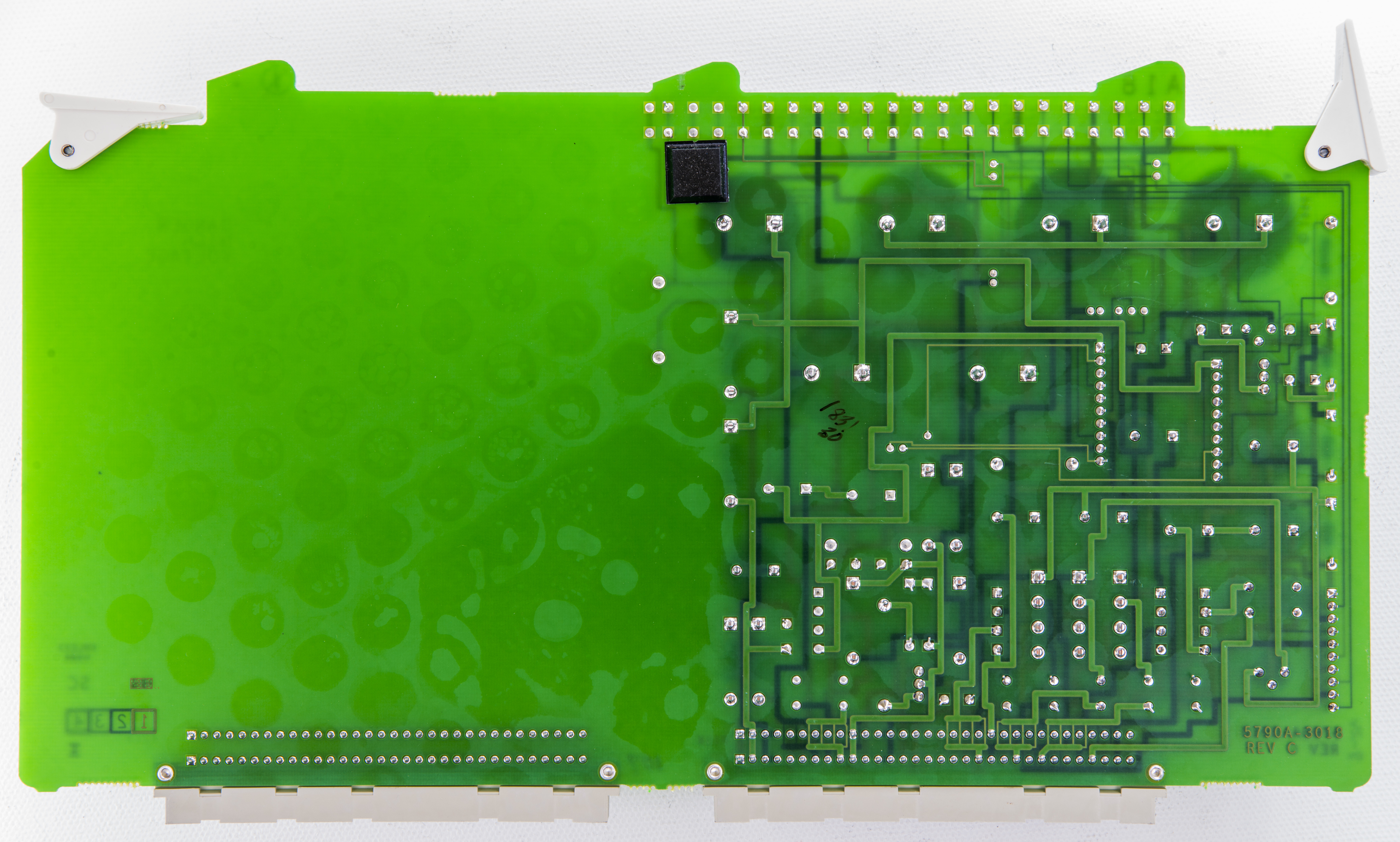
Image 32-33: Fluke 5790A A18 pre-regulator assembly, top and bottom sides.
Semi-empty assembly with regulators and filter caps. There is no need for high voltages in 5790A, so related supply part is completely missing.
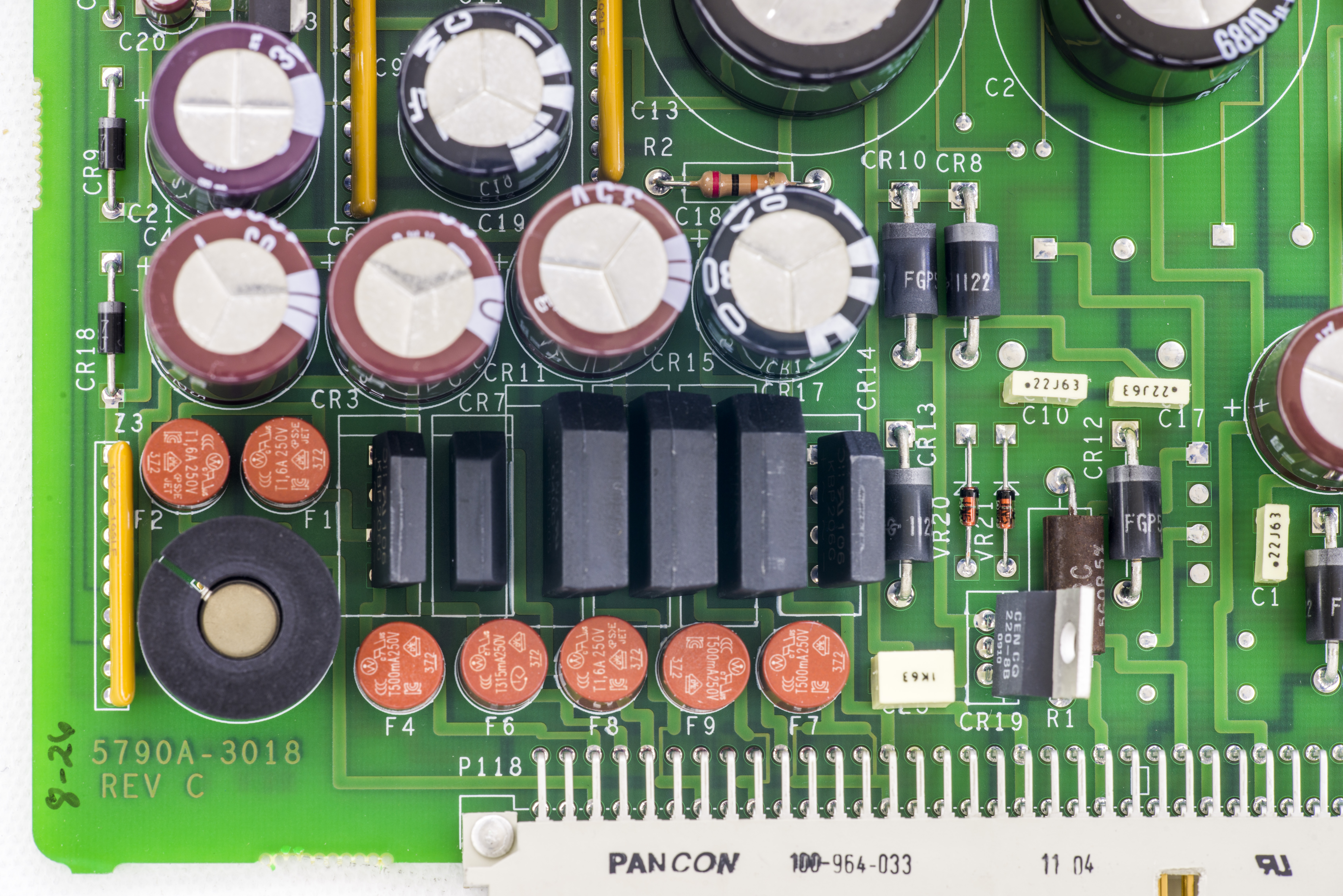
Image 34: Fluke 5790A A18 input rectifiers and fuse protection
A19 PCBA – Out-guard power supply
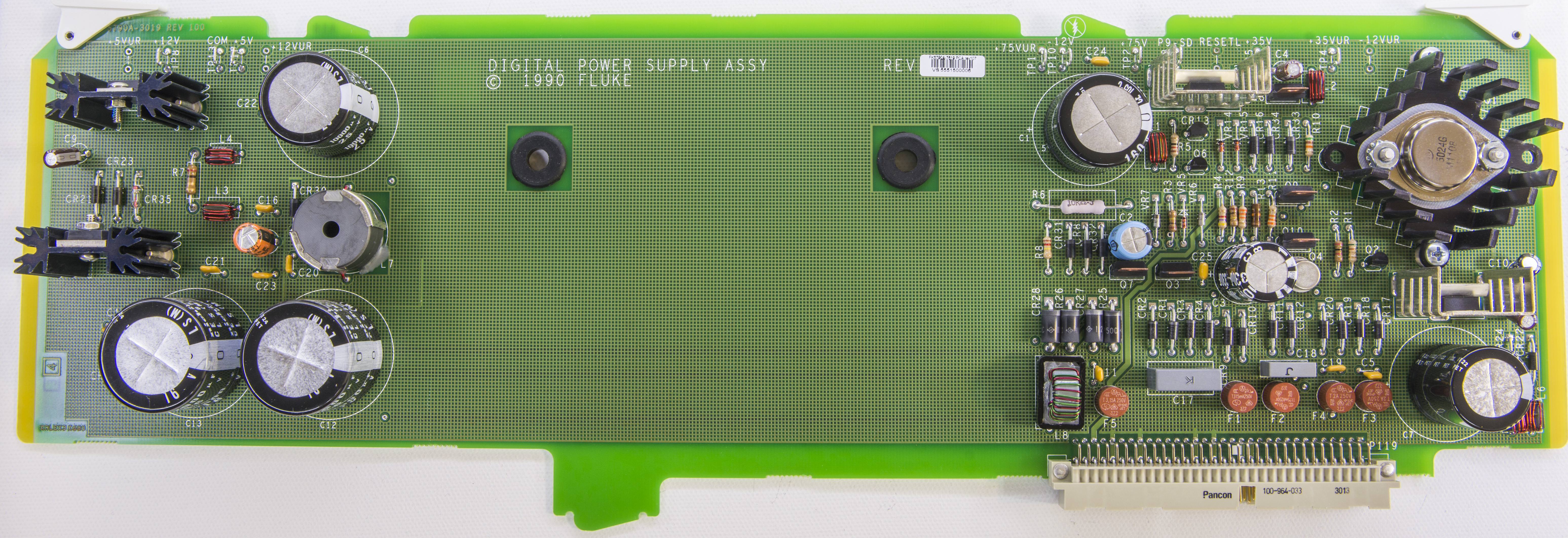
Image 35: Fluke 5790A A19 outguard power supply board
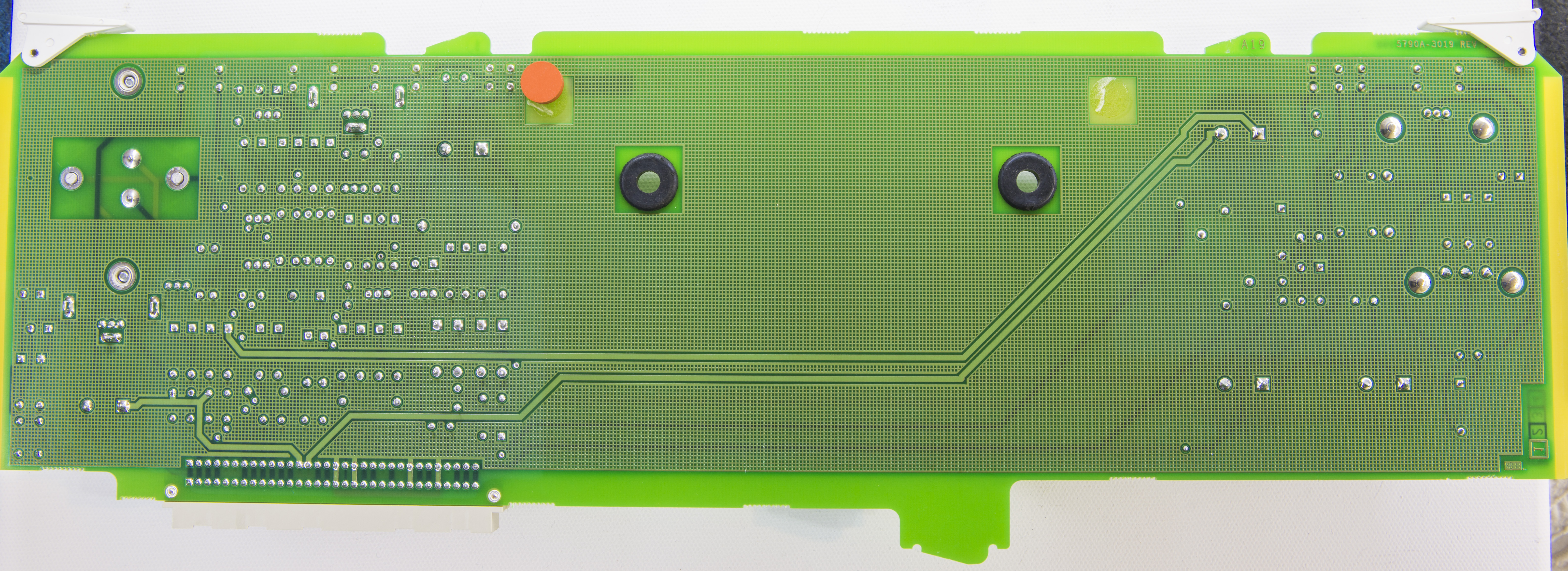
Image 36: Fluke 5790A A19 back
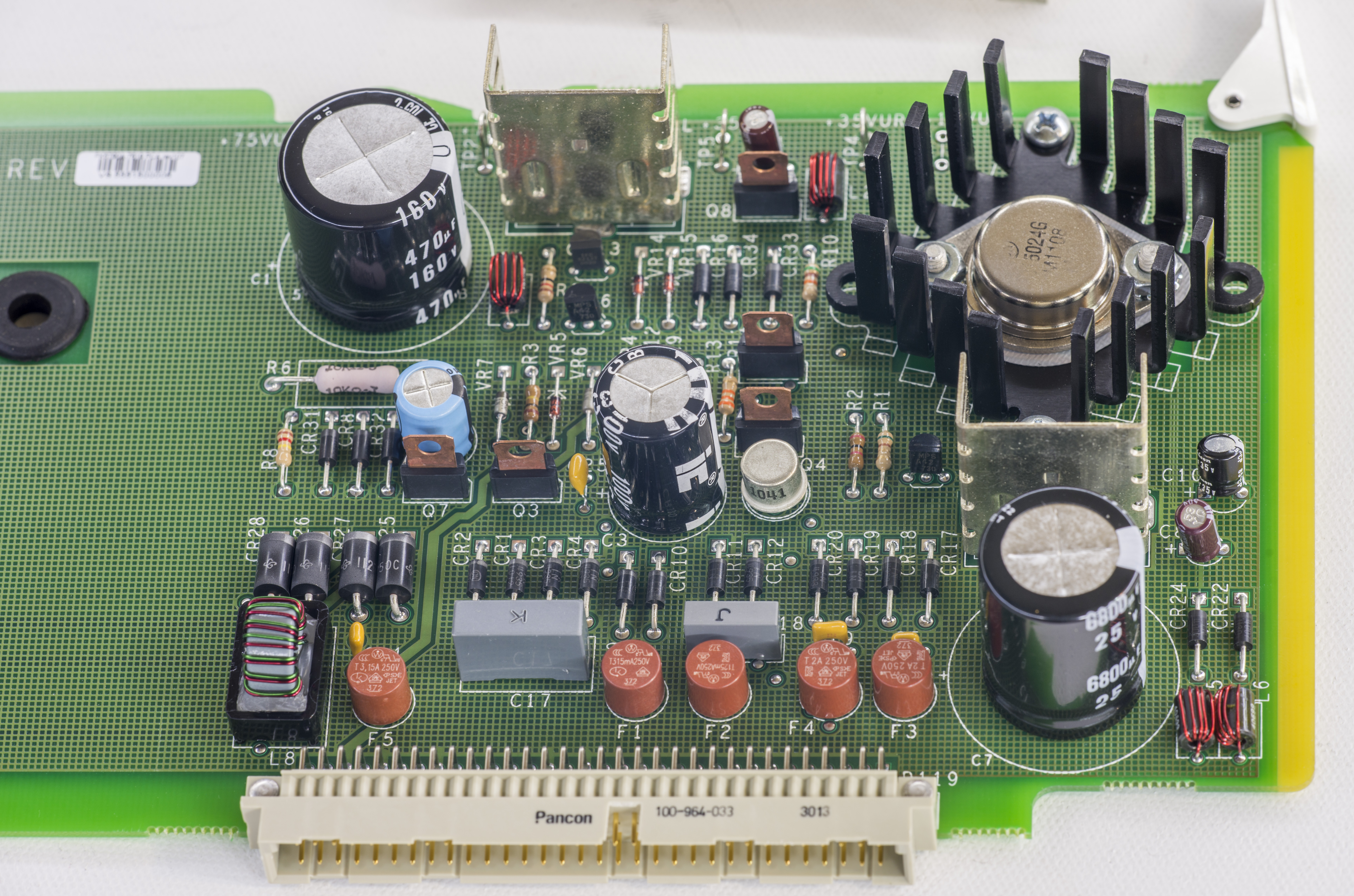
Image 37: Fluke 5790A A19 capacitors and regulators
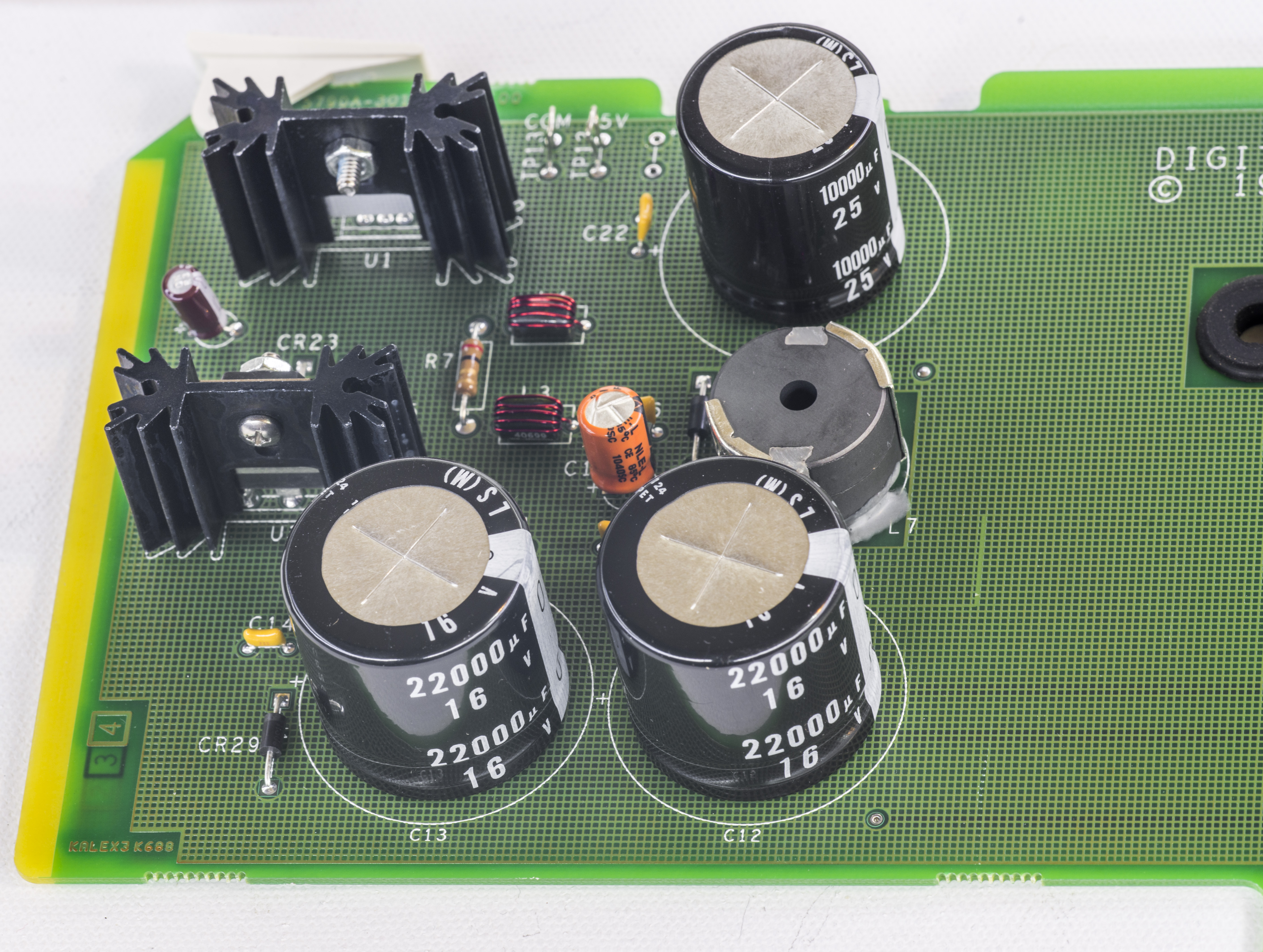
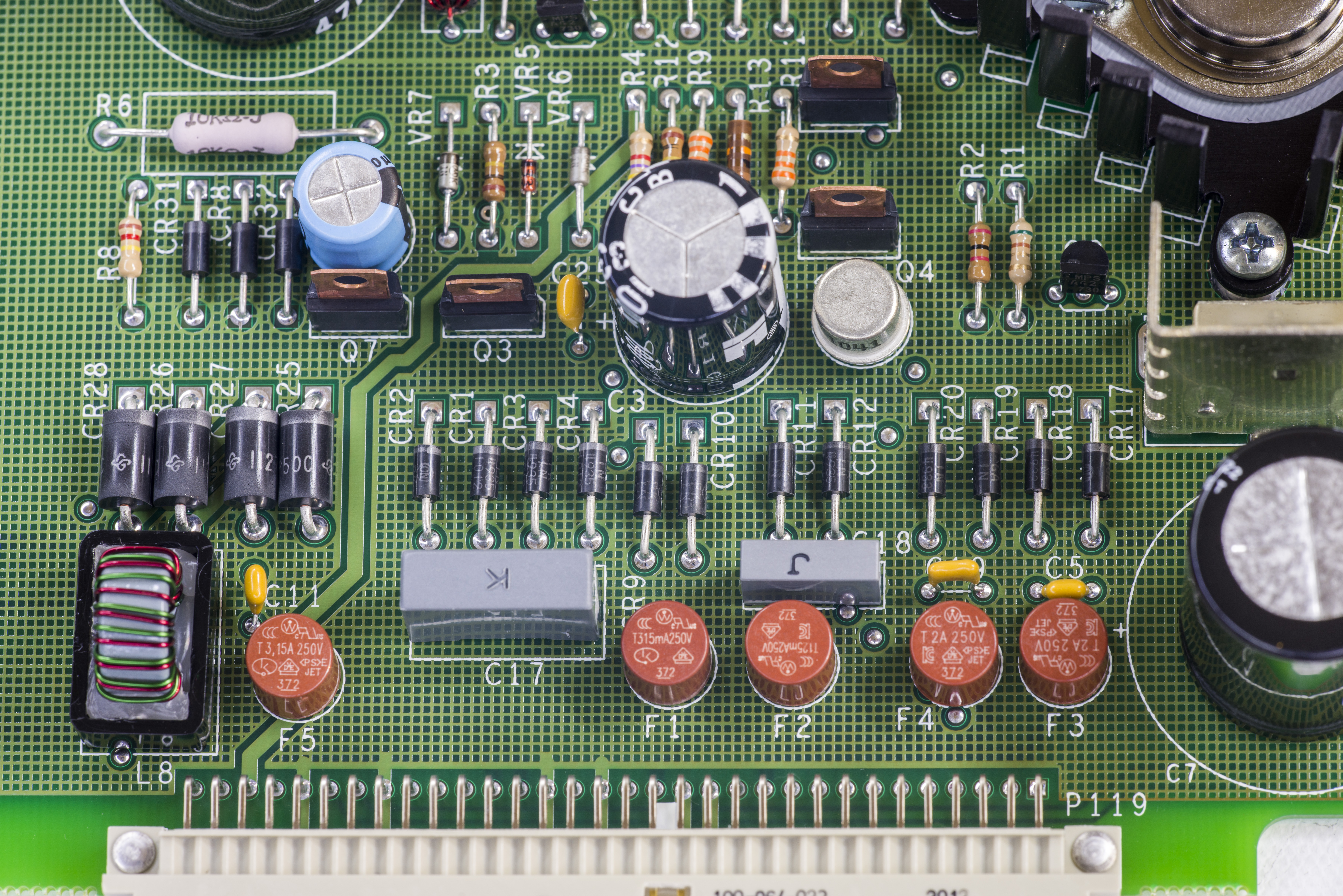
Image 38-39: Fluke 5790A A19 regulators and fuse protection

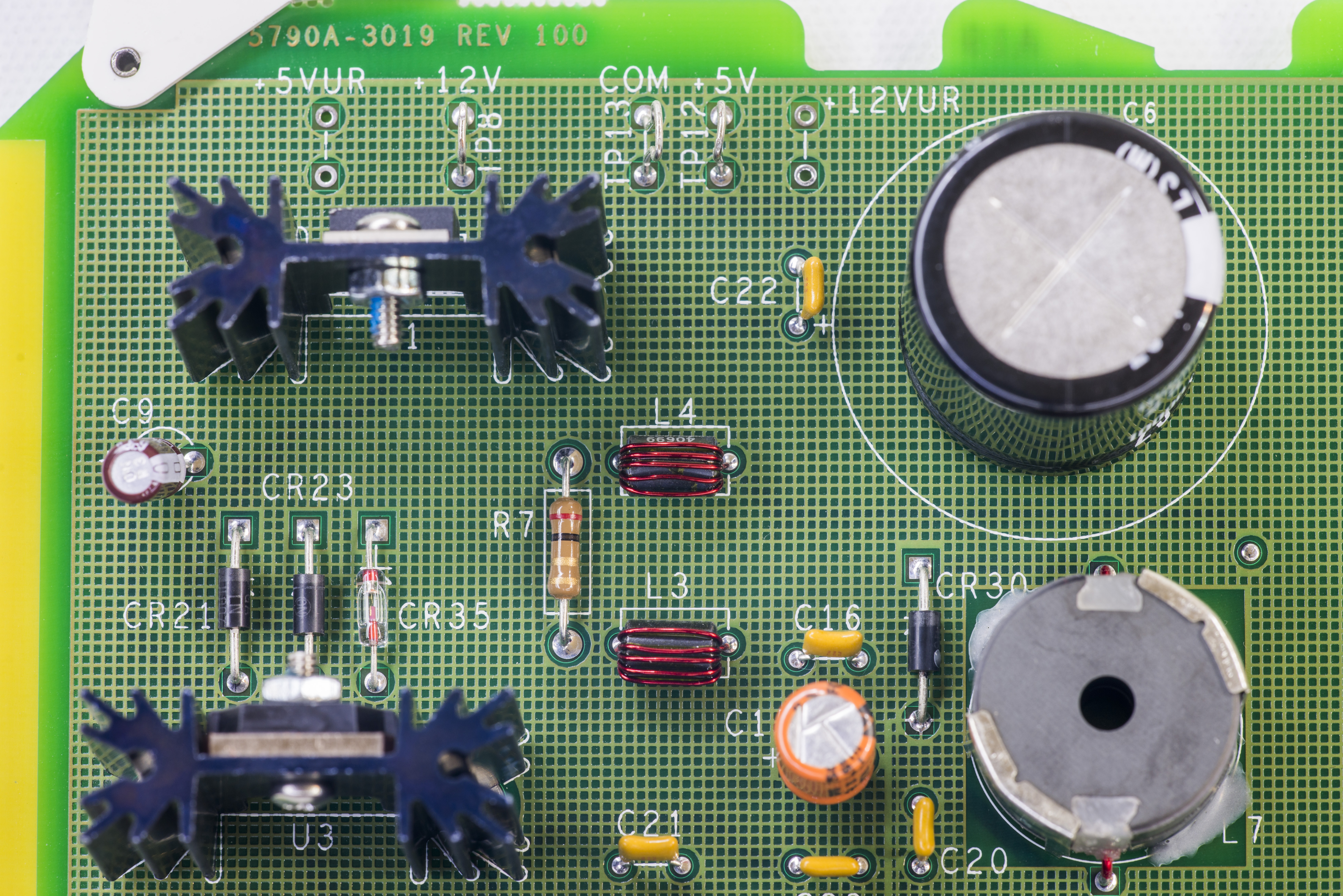
Image 40-41: Fluke 5790A A19 circuits and LDOs with heatsinks
A20 PCBA – Fluke 5790A main processor
This module contains all the digital “brains” of the instrument. It’s newer SMT version. Same board used in modern 5720A’s.

Image 42: Fluke 5790A A20 digital out-guard assembly
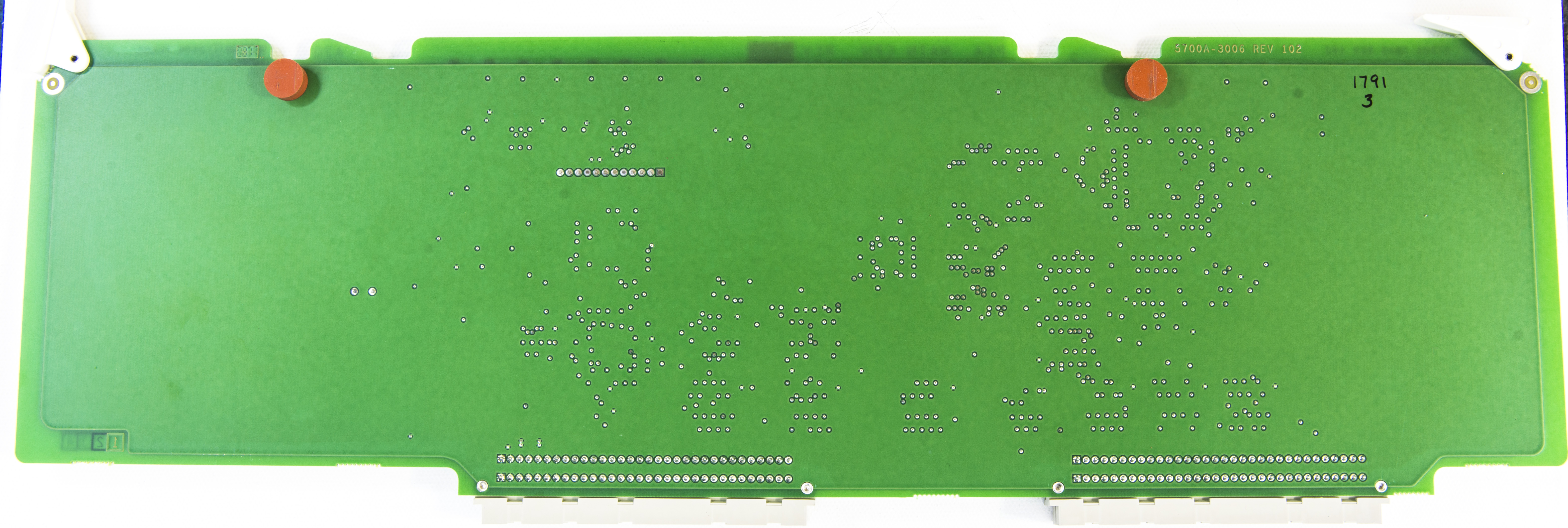
Image 43: Fluke 5790A A20 digital assembly back
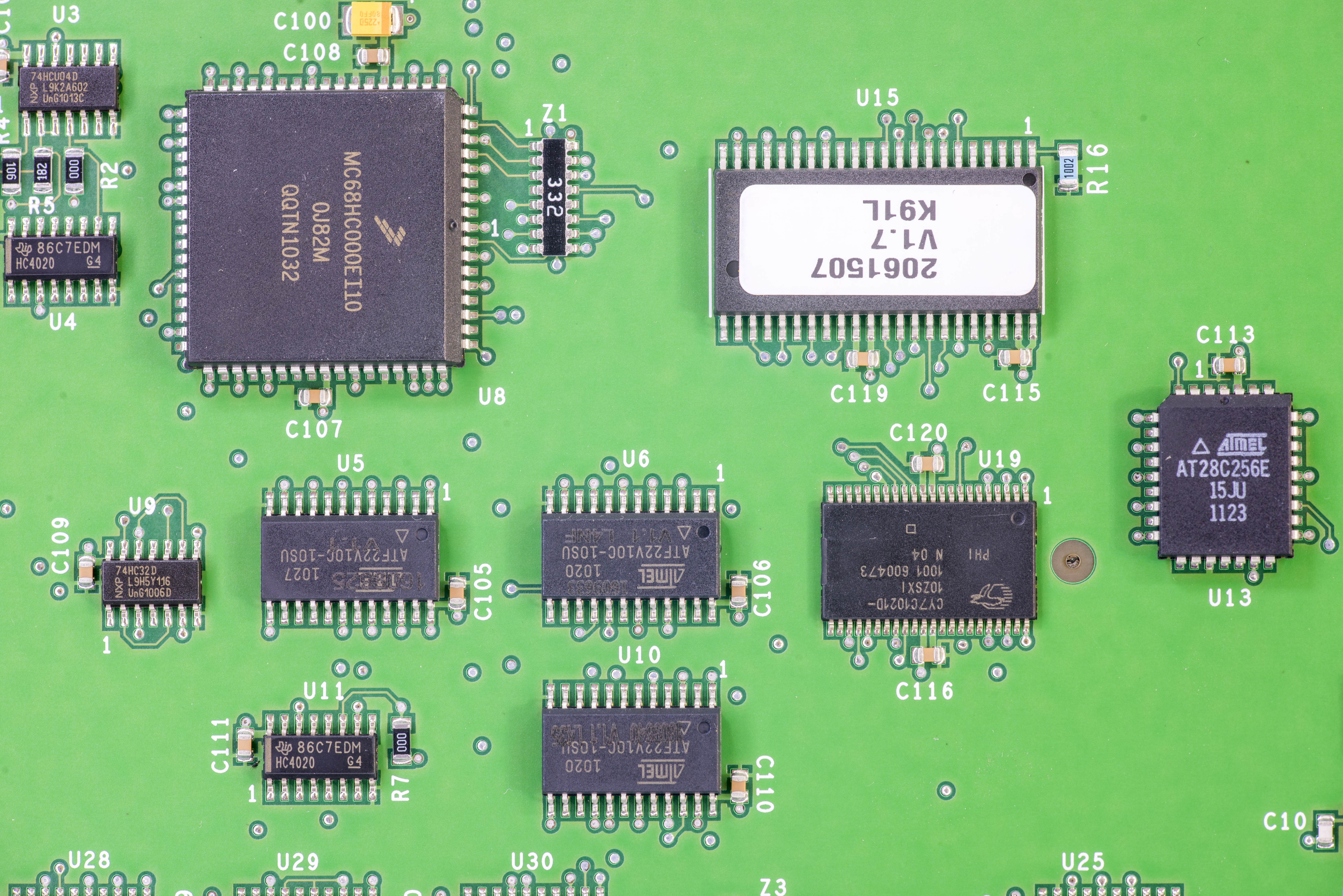
Image 44: Fluke 5790A A20 processor section
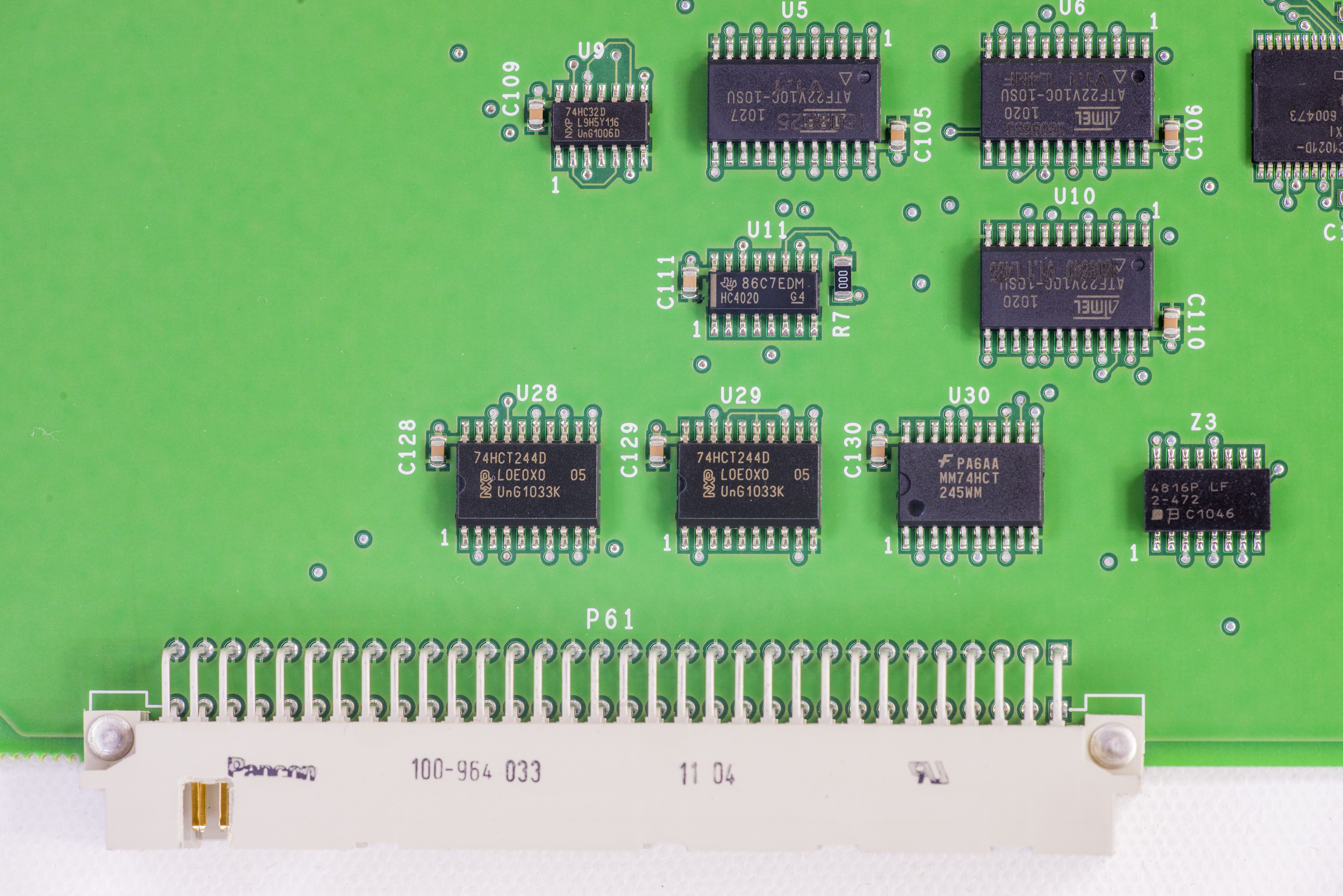
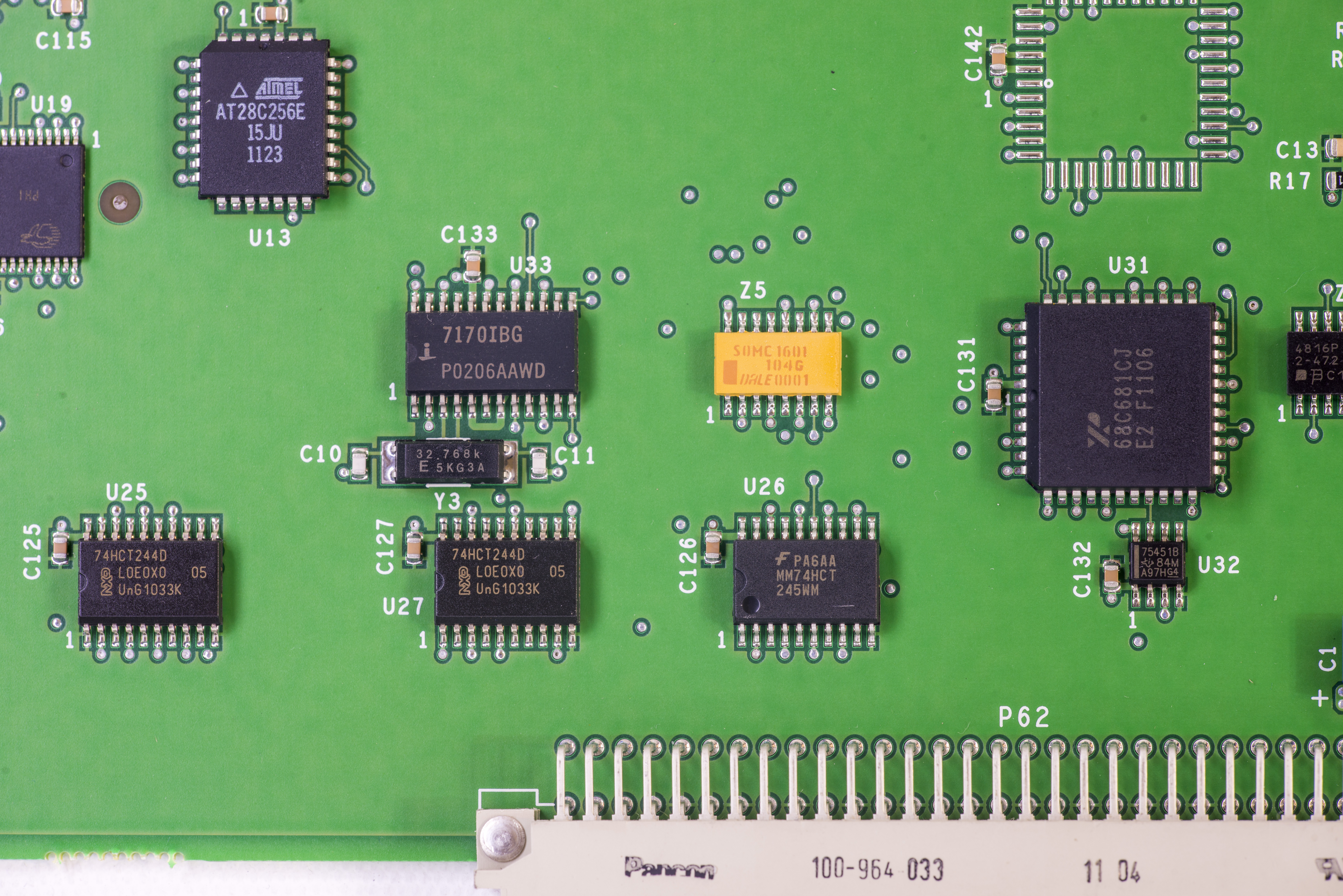
Image 45-46: Fluke 5790A A20 I/O circuits
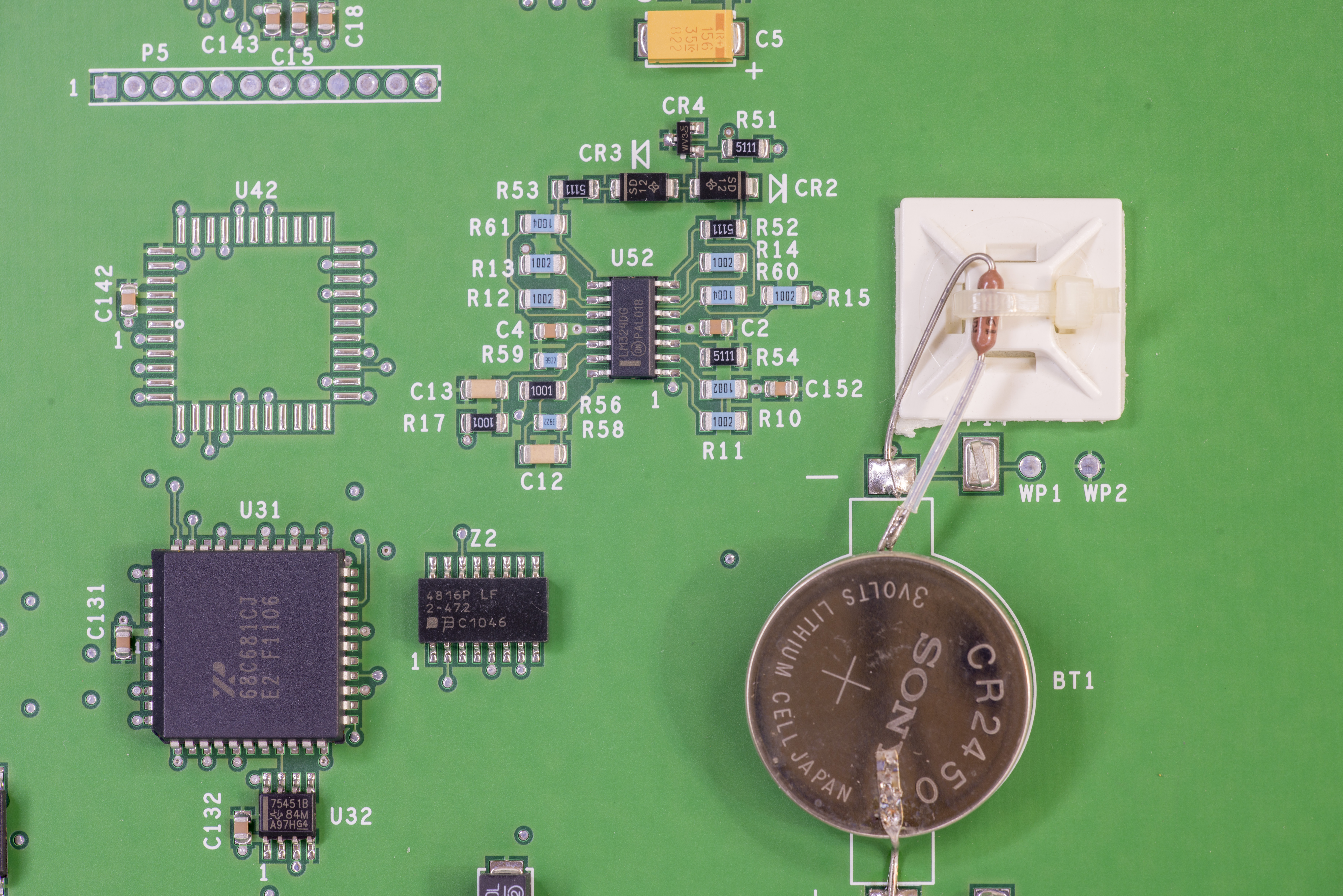
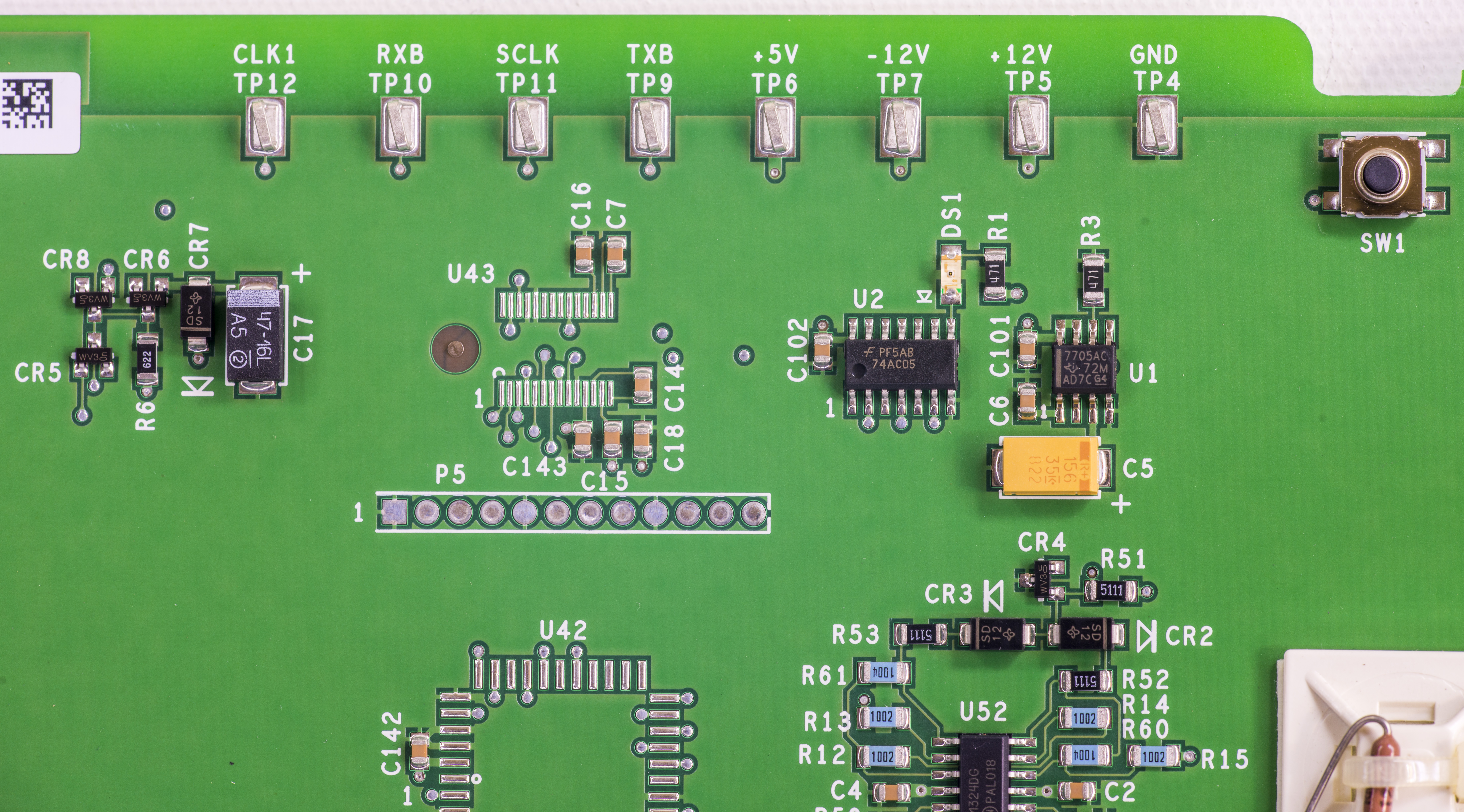
Image 47-48: Fluke 5790A A20 RTC battery and test points
Front panel assembly
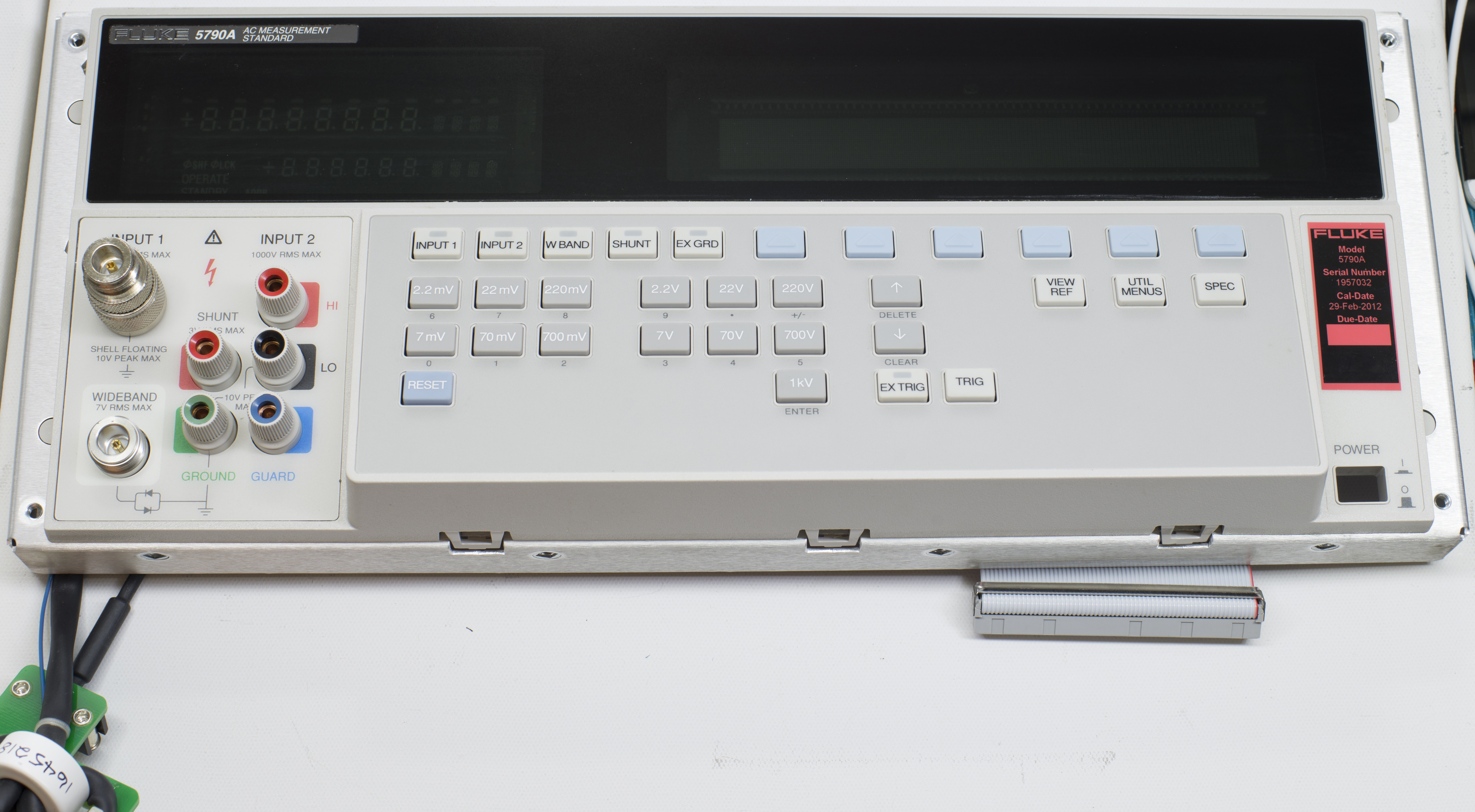
Image 49: Fluke 5790A front panel assembly
Front panel is very same to 57xx. VFD glass is exact.
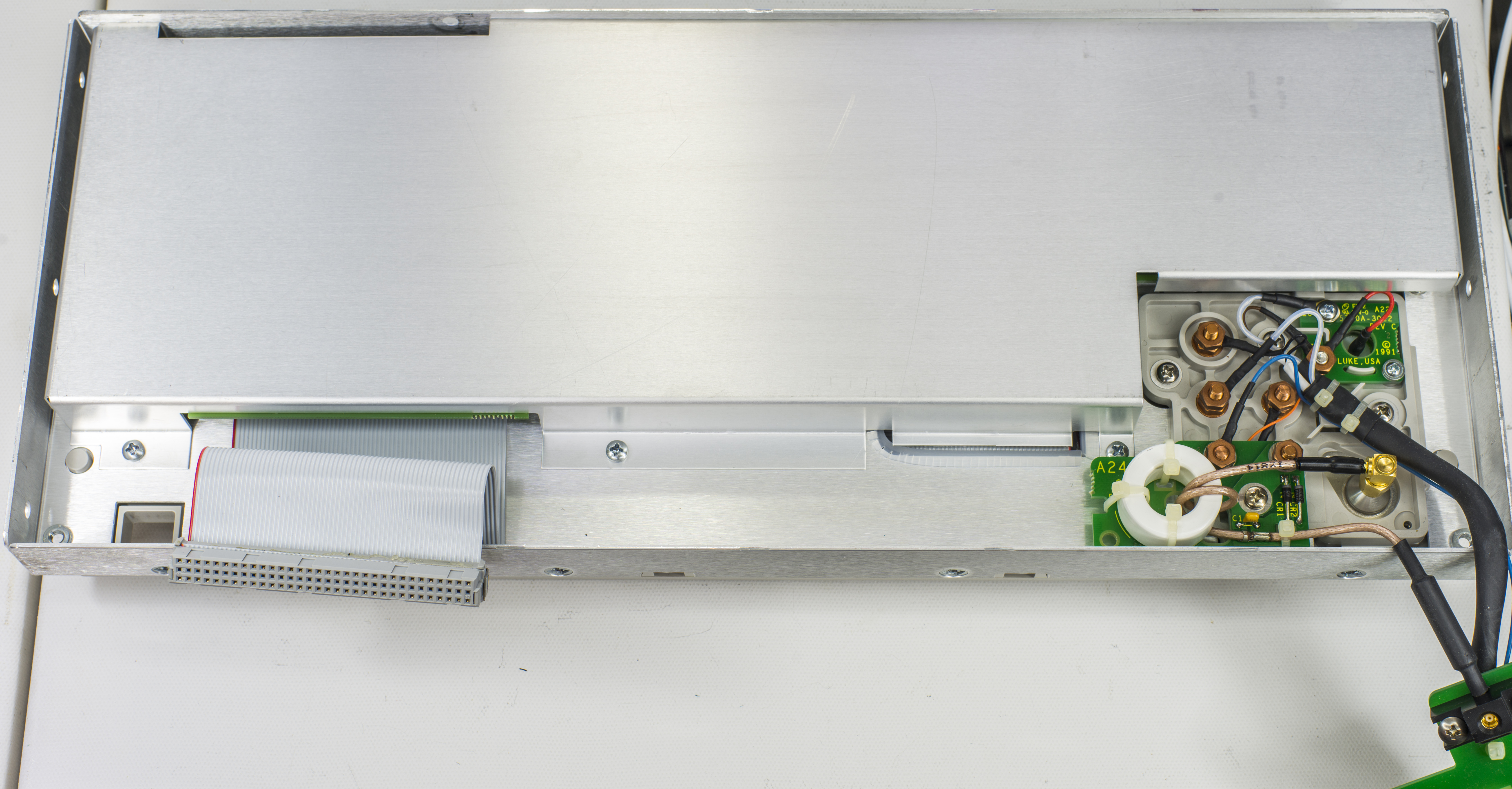
Image 50: Fluke 5790A front panel assembly, fully shielded back

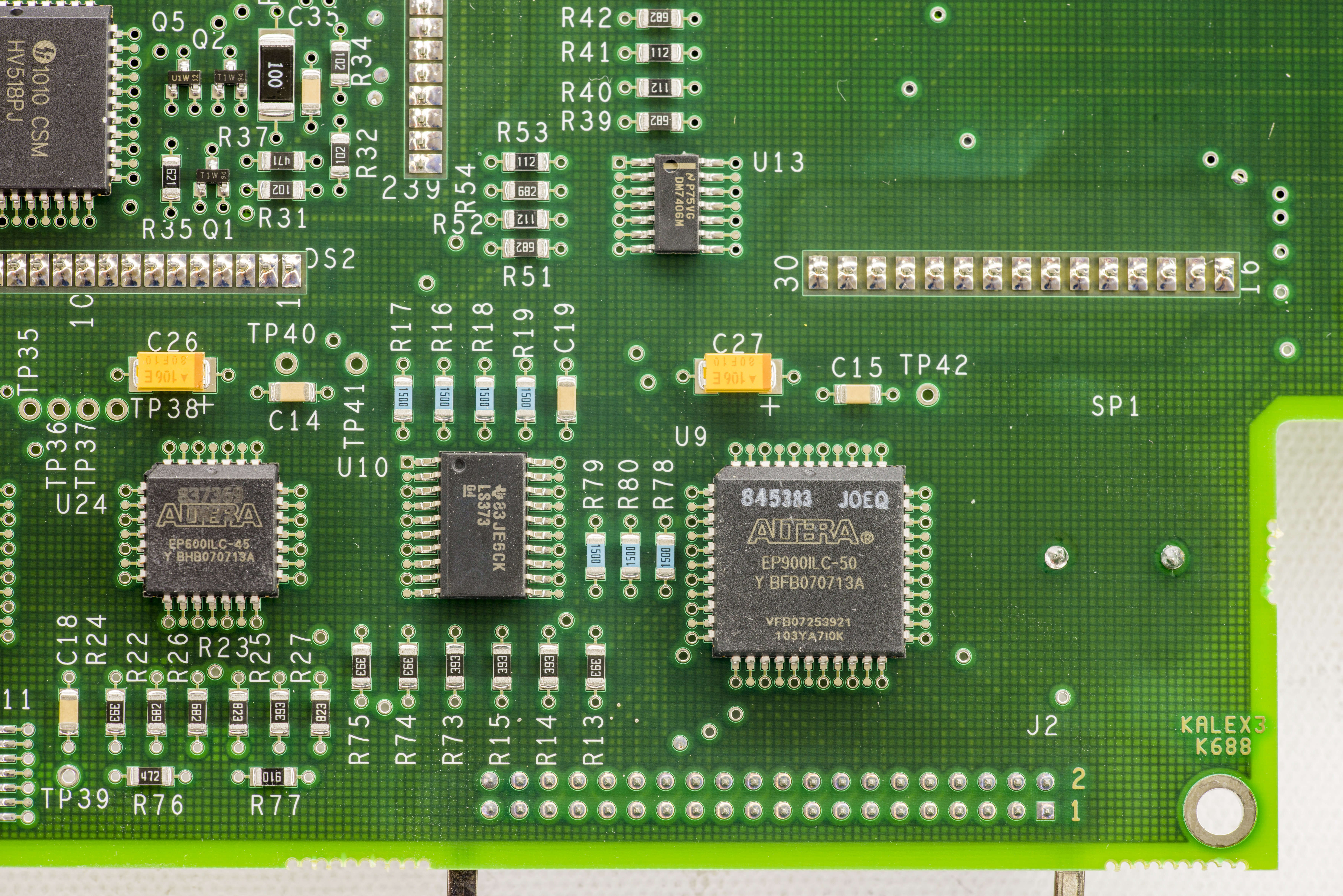
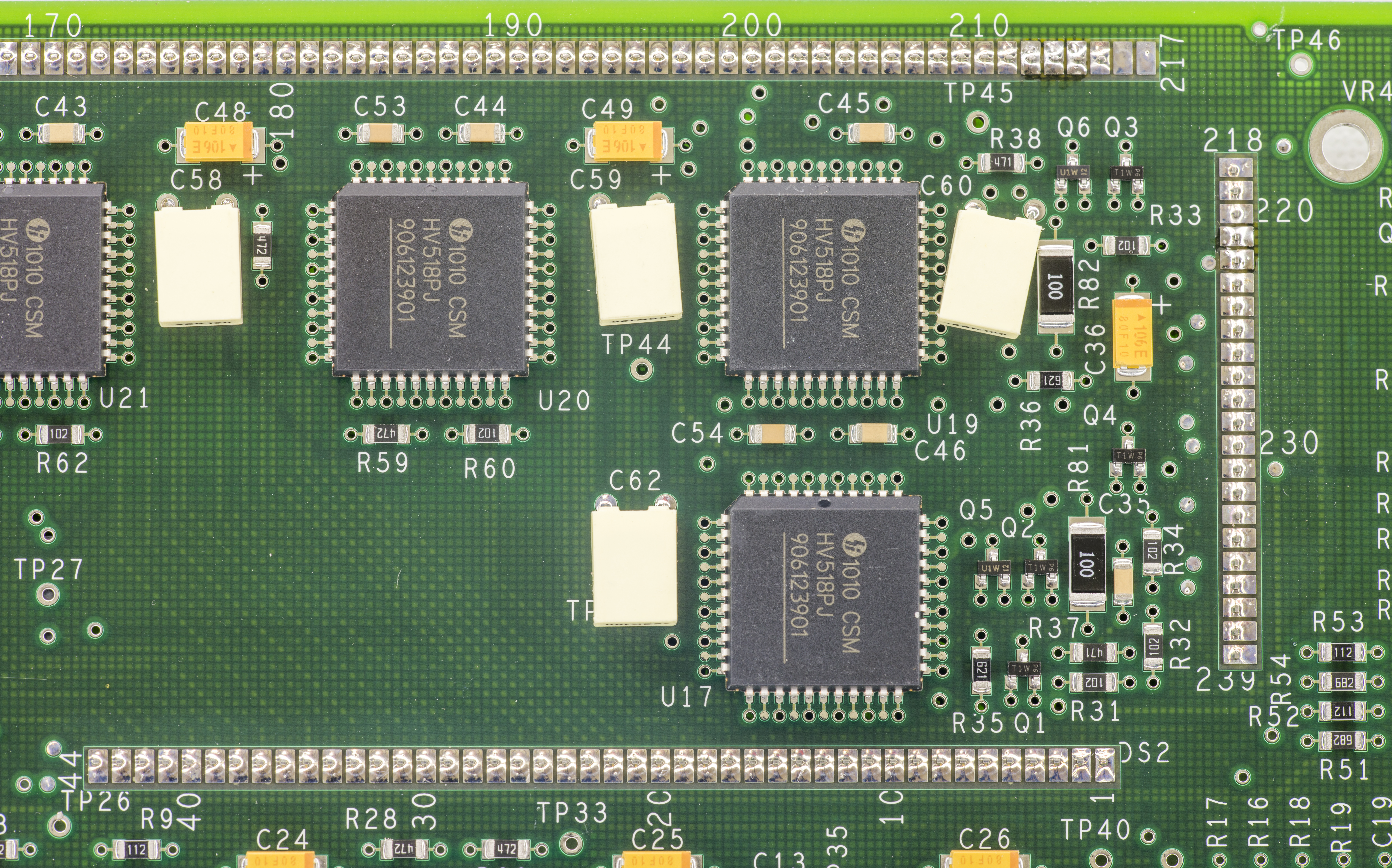
Image 51-53: Fluke 5790A VFD high-voltage drivers
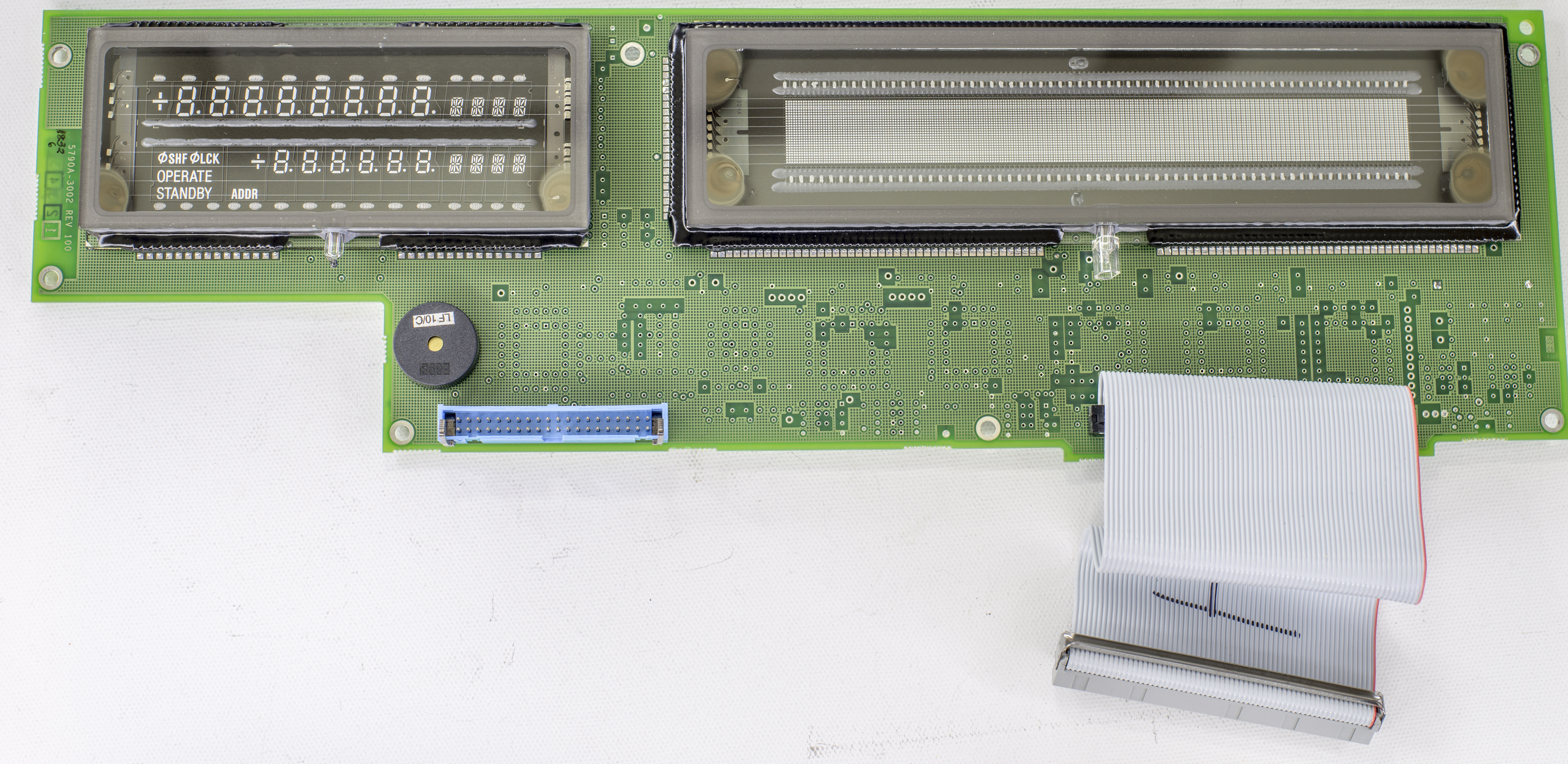
Image 54: Fluke 5790A A2 front panel board with VFD display

Image 55: Fluke 5790A A2 front panel board with VFD display, back

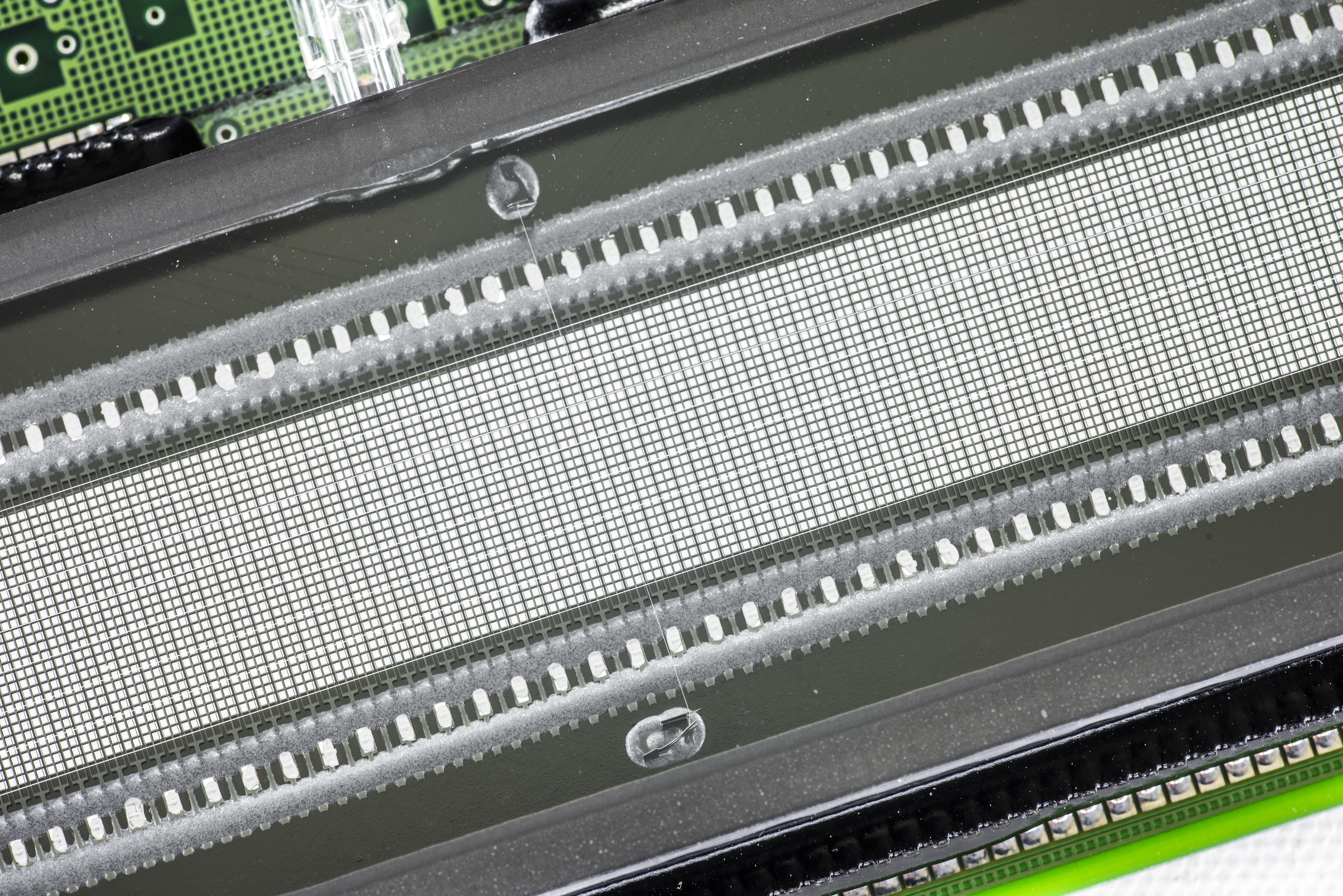
Image 56-57: Fluke 5790A A2 VFD glass
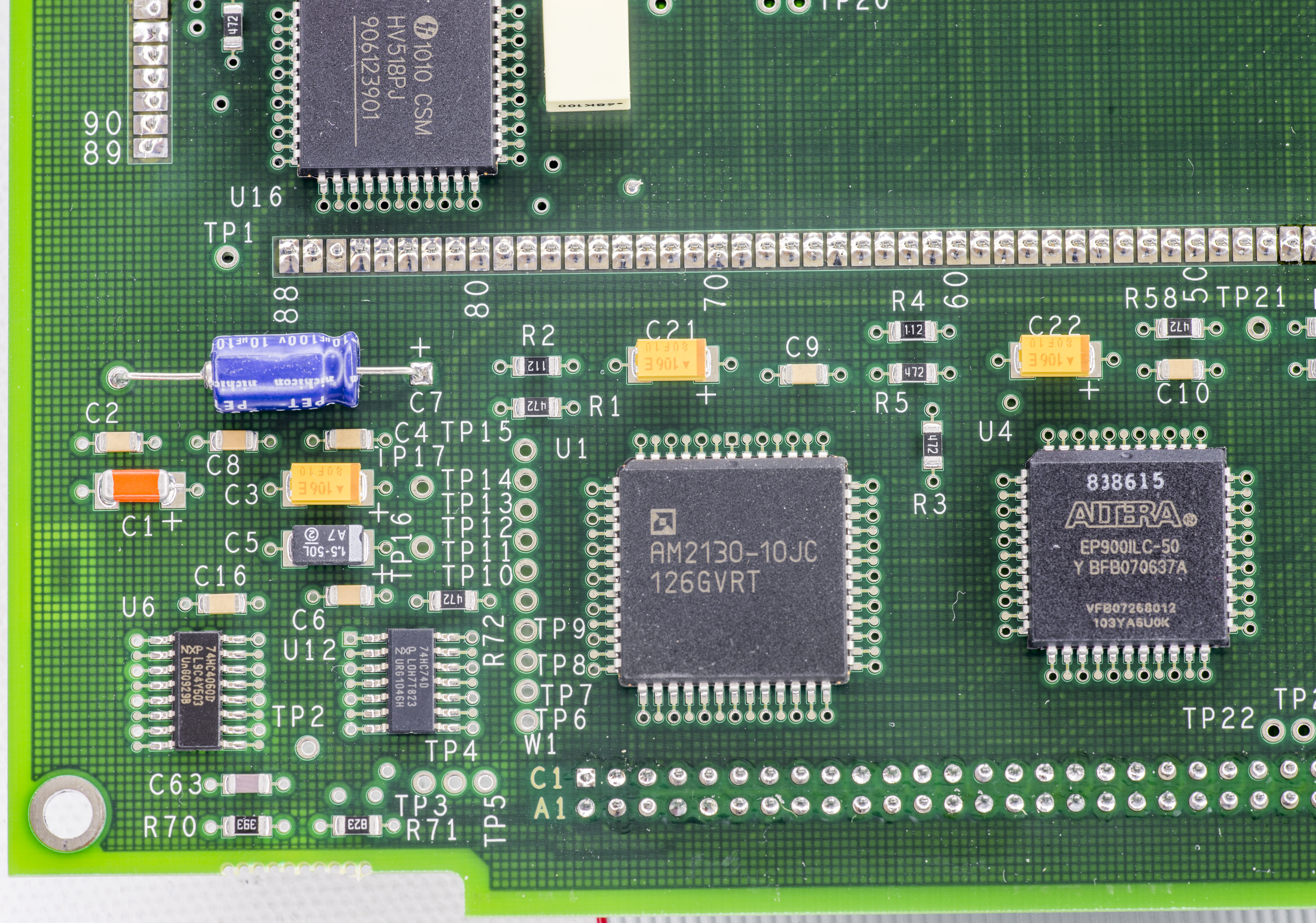
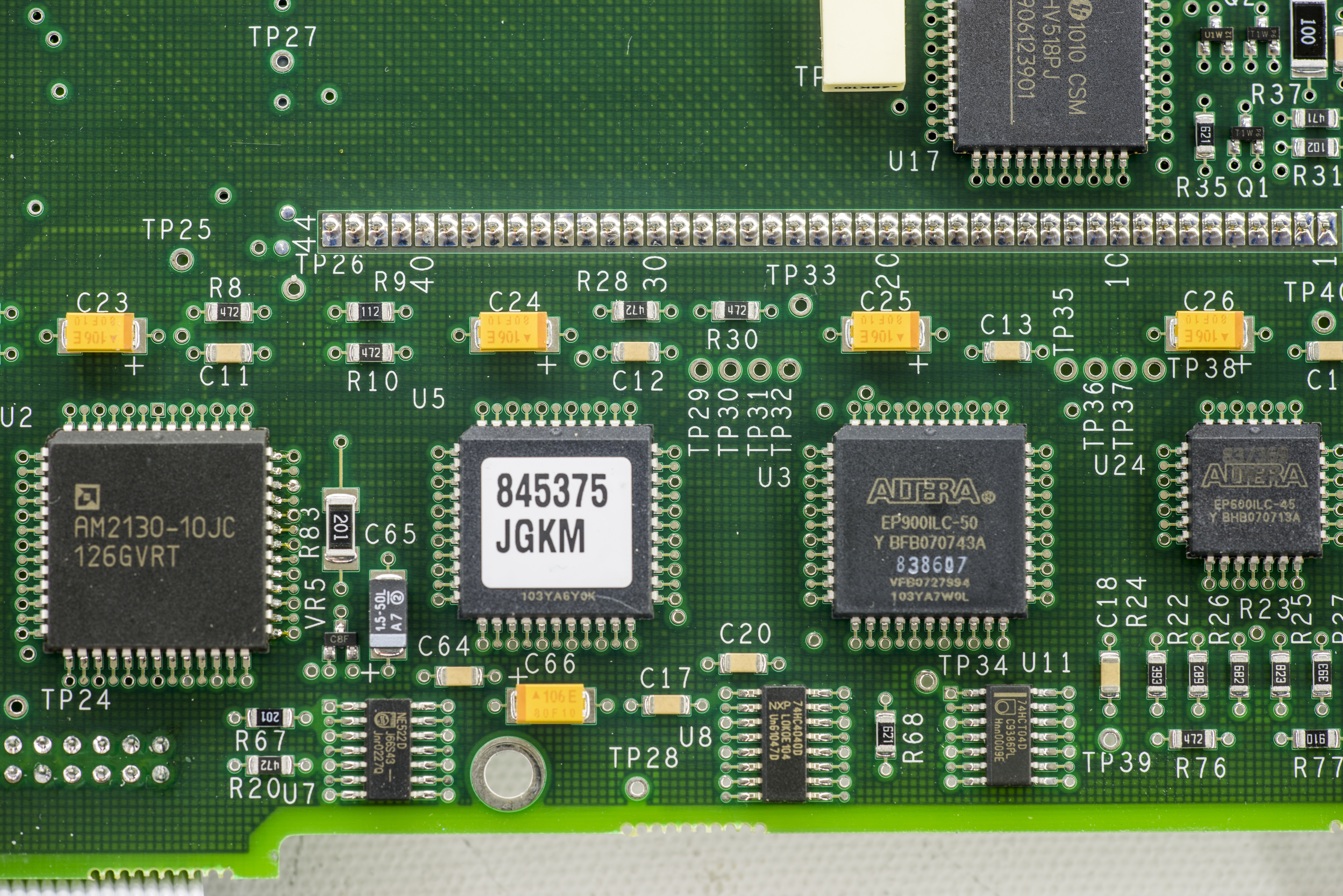

Image 58-60: Fluke 5790A A2 more driver logic and label
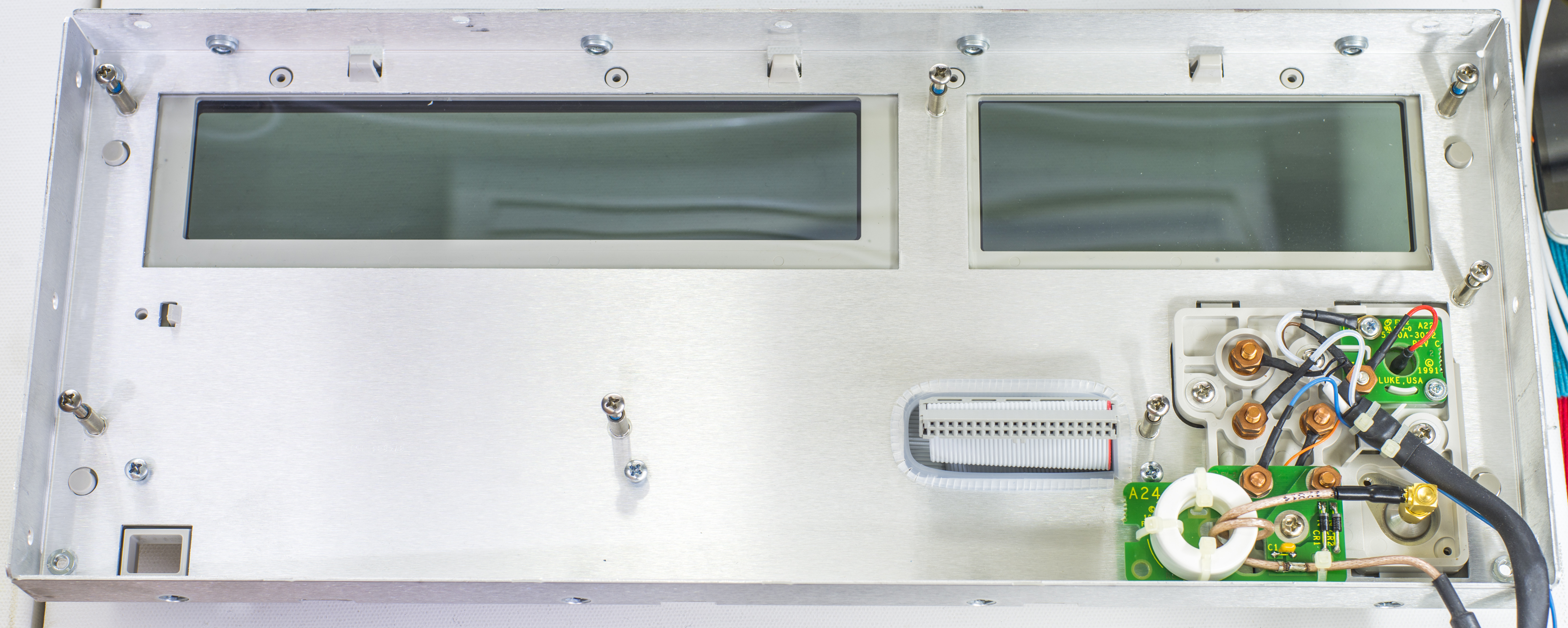
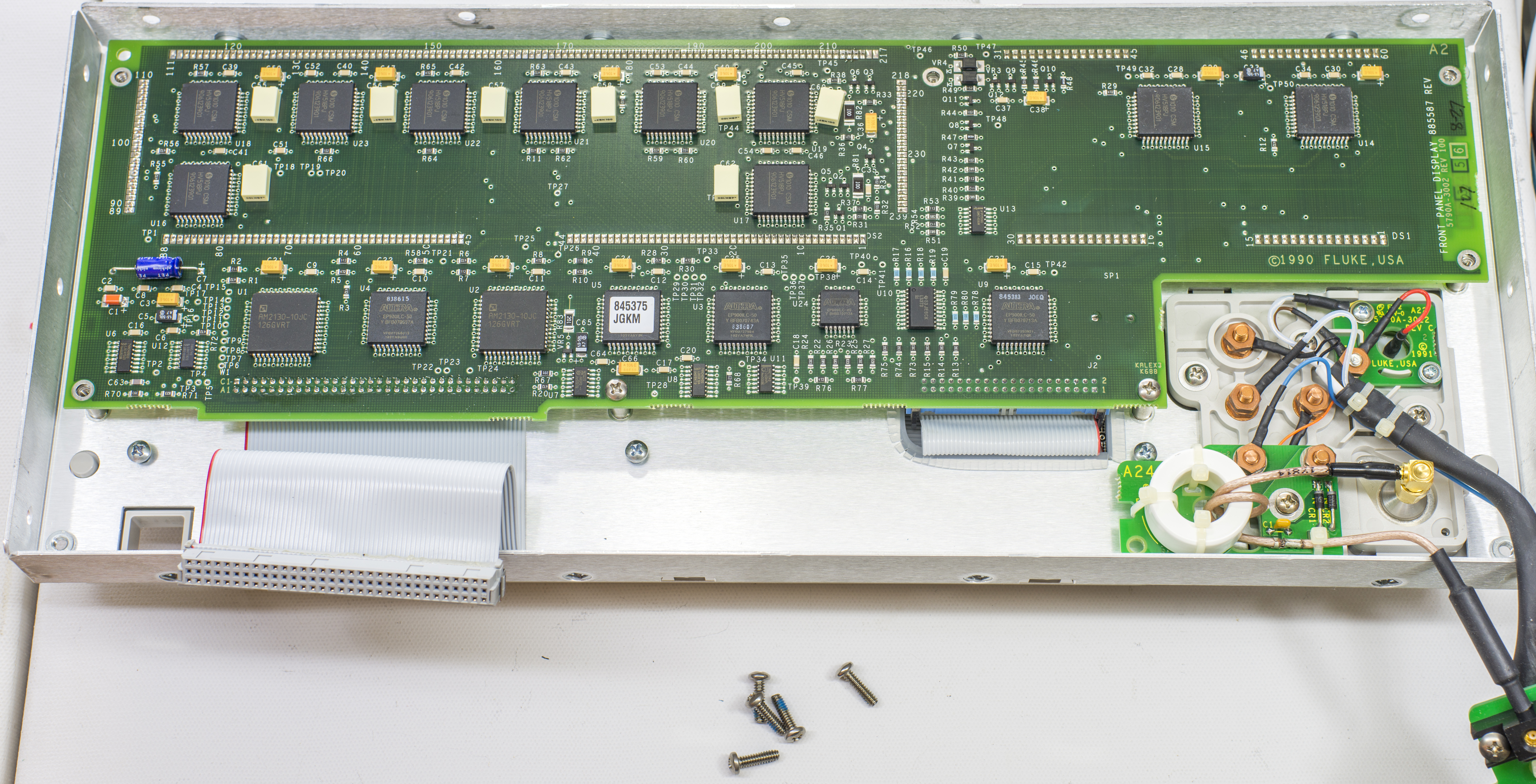
Image 61-62: Fluke 5790A A2 location and frame
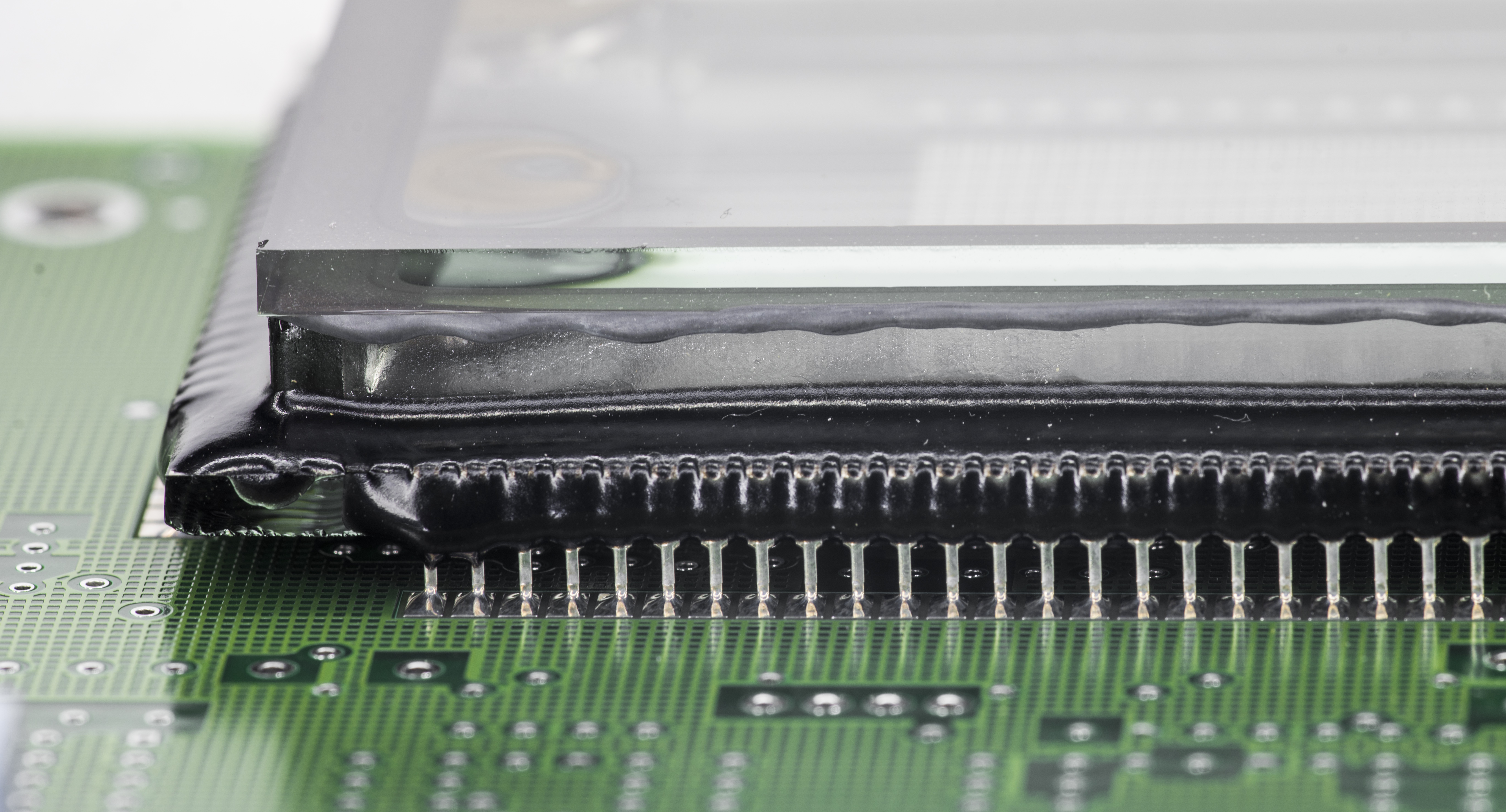
Image 63: Fluke 5790A display glass assembly
Connector assembly for front panel had own little cute boards.
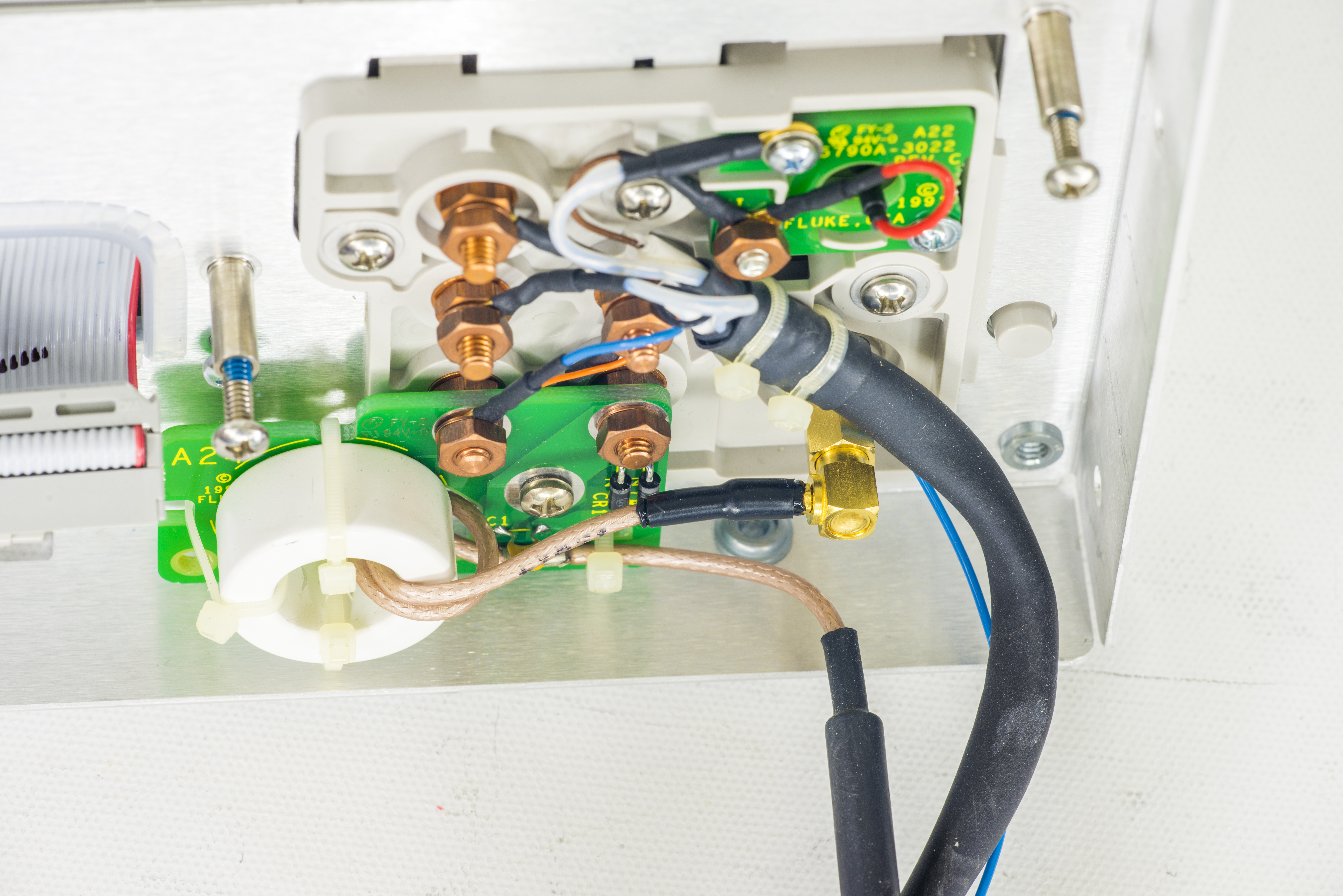

Image 64-65: Fluke 5790A front terminals low-thermal copper connections

Image 66-67: Fluke 5790A shield part numbers
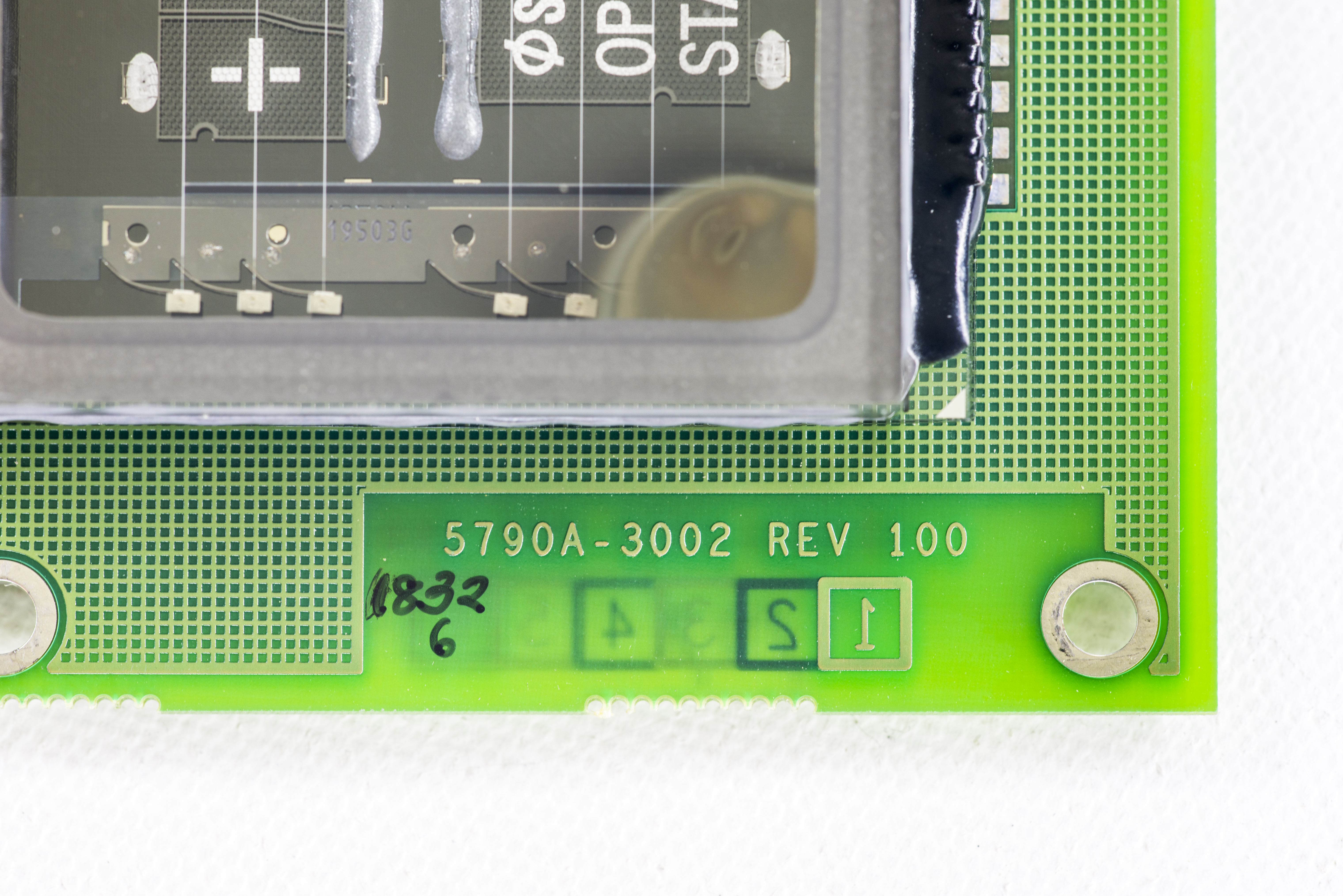

Image 68-69: Fluke 5790A PCB marking, 6-layer count and I/O connector with hooks
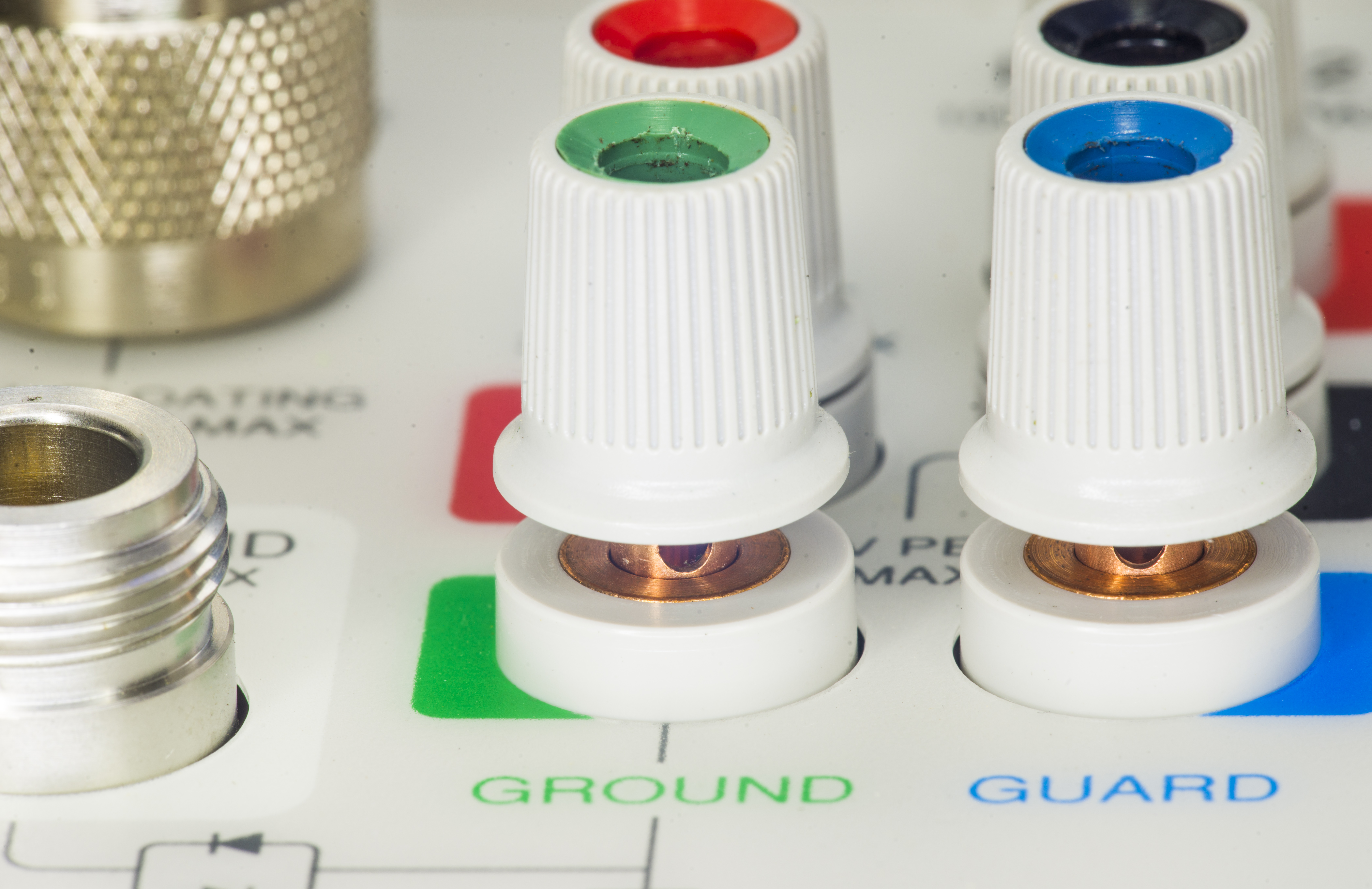
Image 70: Fluke 5790A bare-copper low-thermal 5-way binding posts
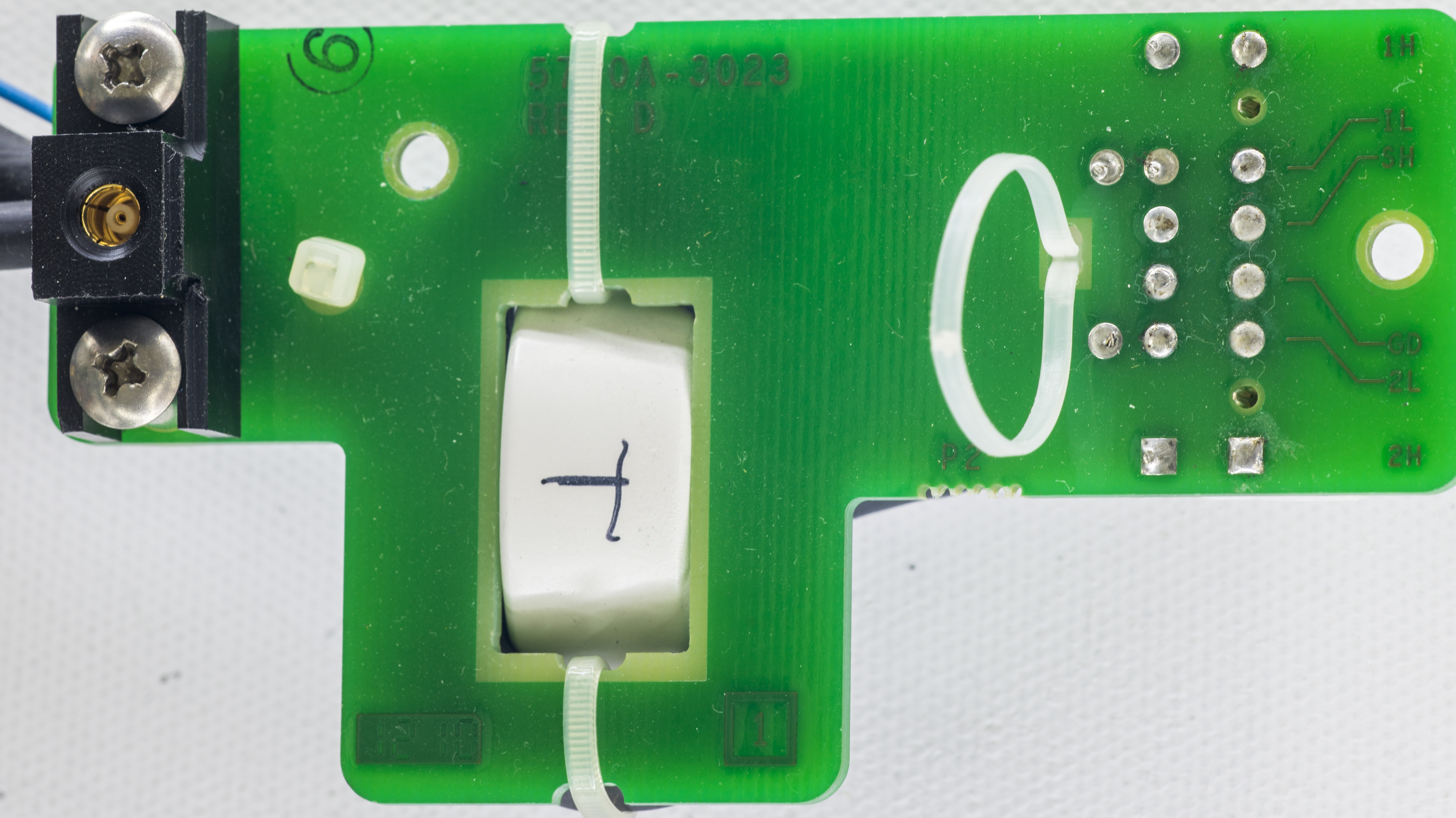
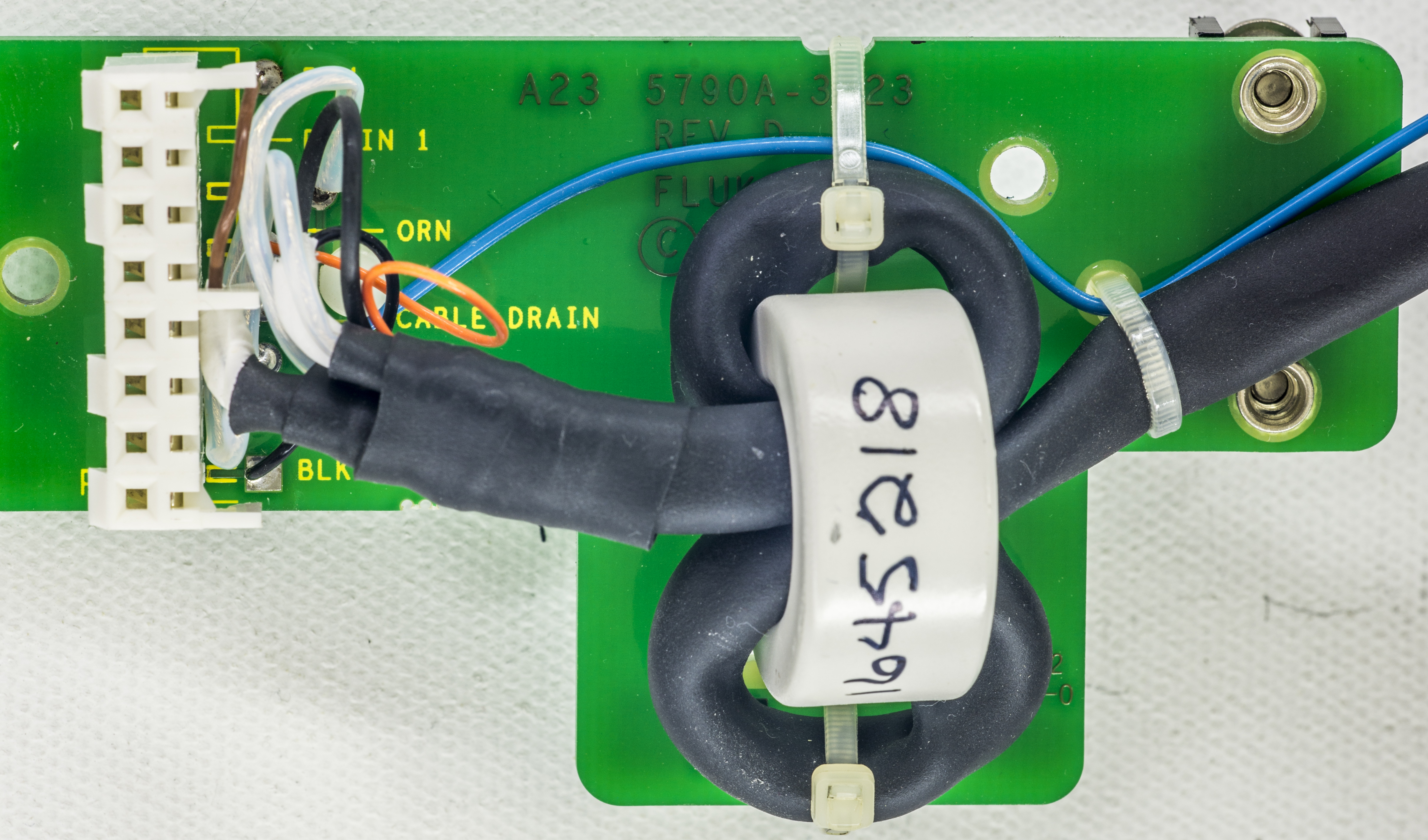
Image 71-72: Fluke 5790A wiring connection board assembly
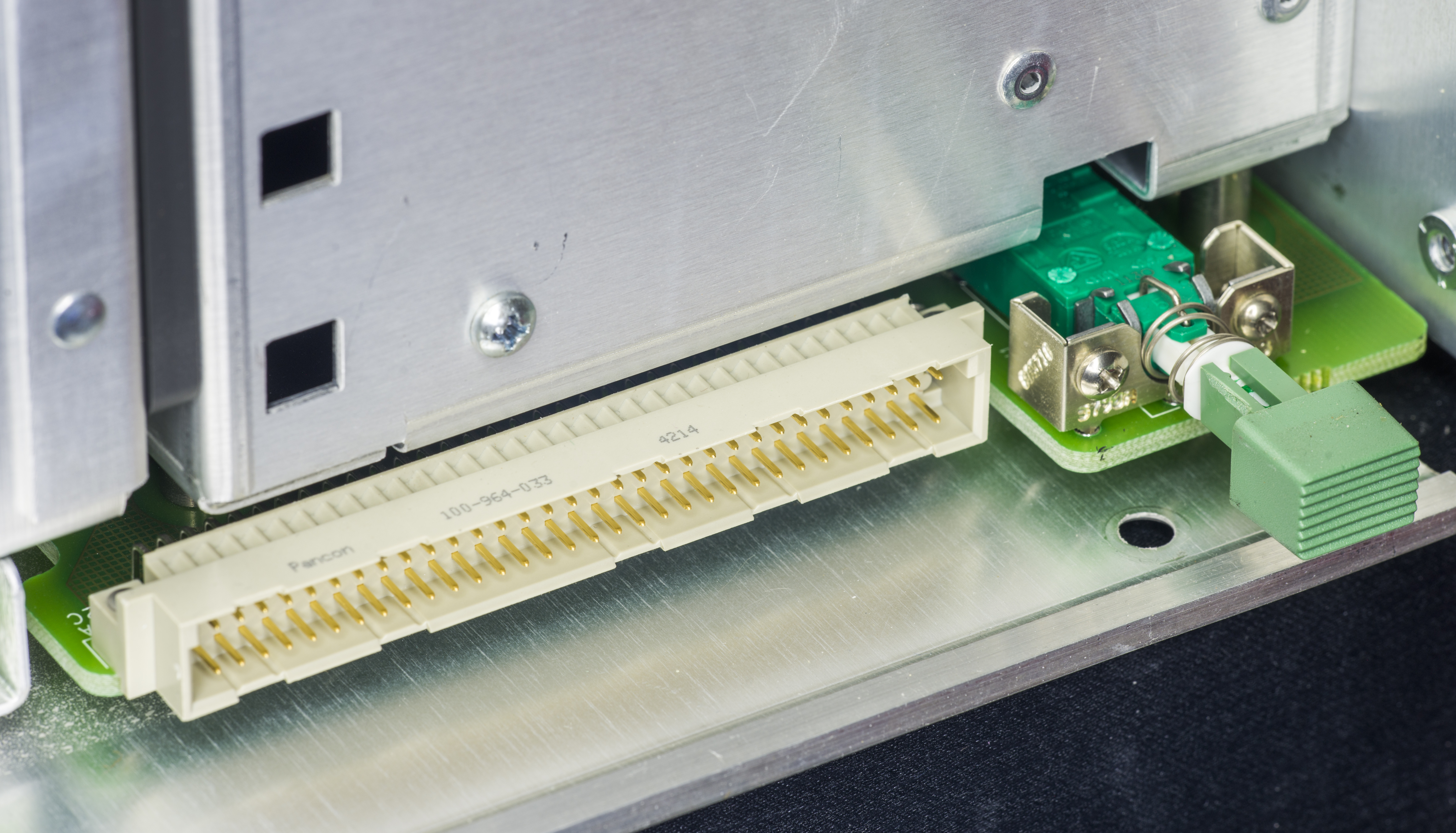
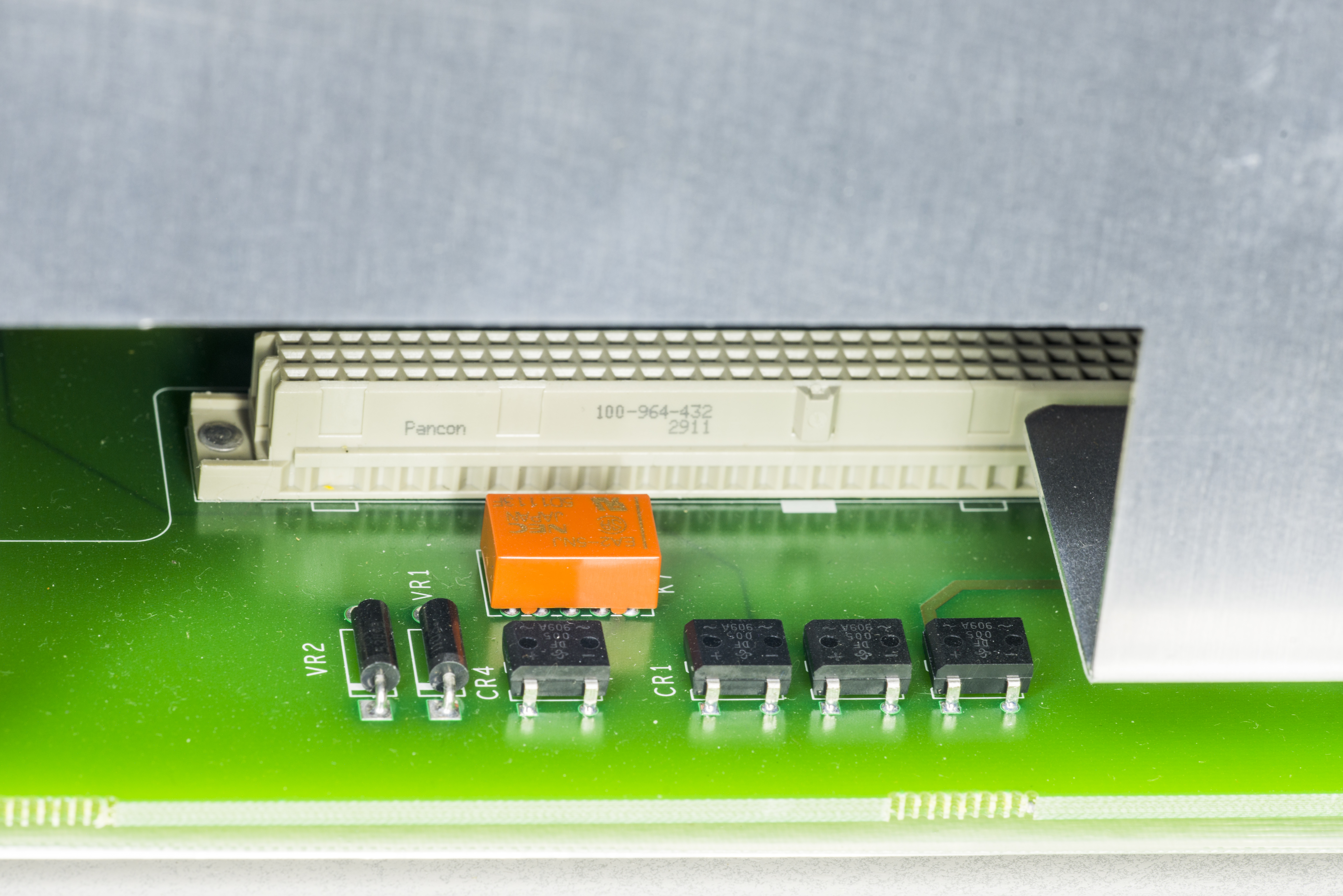
Image 73-74: Fluke 5790A front panel connector and input power switch on A4 board
Troubleshooting
FAULT? = 103,"Cal/Diag not Halted"
FAULT? = 409,"A10 Transfer: Dormant Protection Check"
FAULT? = 413,"A10 Transfer: LO V Input Path"
FAULT? = 413,"A10 Transfer: 220V Input Path"
FAULT? = 413,"A10 Transfer: 22V Input Path"
FAULT? = 410,"A10 Transfer: Overload Check"
FAULT? = 412,"A10 Transfer: 7 mV Range Zero"
FAULT? = 412,"A10 Transfer: 22 mV Range Zero"
FAULT? = 408,"A10 Transfer: 2.2V Range"
FAULT? = 408,"A10 Transfer: 7V Range"
FAULT? = 408,"A10 Transfer: 7V Range"
FAULT? = 408,"A10 Transfer: 22V Range"
FAULT? = 408,"A10 Transfer: 22V Range"
FAULT? = 408,"A10 Transfer: 70V Range"
FAULT? = 408,"A10 Transfer: 220V Range"
FAULT? = 1,"Error Queue Overflow"
Essentially what this long list of errors tell us that main front-end circuitry is not working properly and cannot measure anything. In such system failures, often first test would be checking the power supply rails, as that often the culprit and most easy fix.
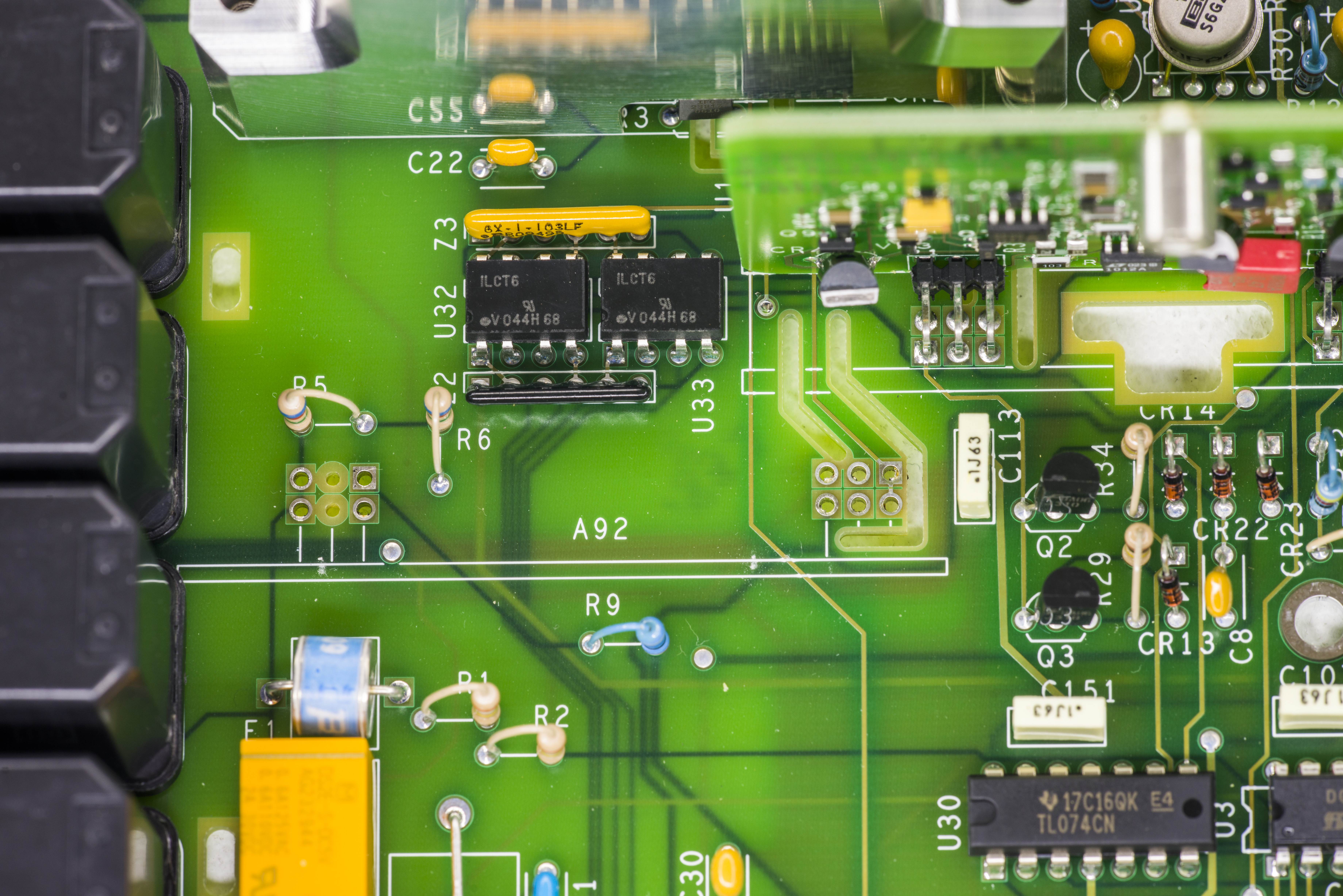
A10 PCBA – Transfer assembly
Take a look at the core of 5790A AC/DC standard. A10 PCBA module handle accurate transfer of input AC or DC voltage by thermal sensor circuitry. Low voltage ranges are amplified by this assembly as well.
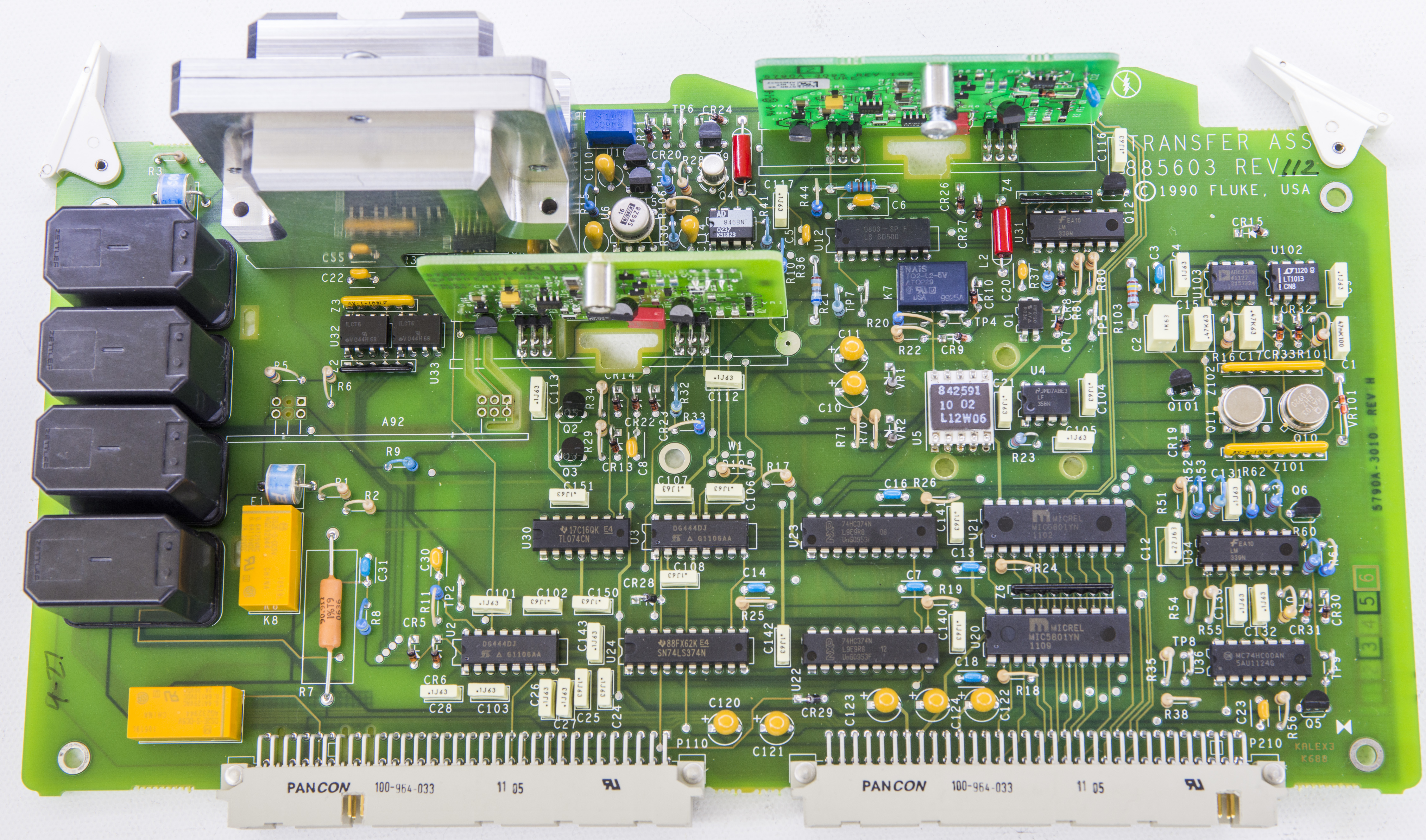
Photo above have A92 protection module removed during diagnostics. Silver metal block on top is high-voltage attenuator block for 7V/22V/70V/220V ranges. It is made around 45k/4.5k/500 Ω custom Fluke resistor network, enclosed in massive aluminum block. Vertical modules are precise amplifiers for low voltage ranges, build with opamps and discrete stages. There is 2.2mV/7mV amplifier onboard as well, built around Analog Device AD846BN (now obsolete :(( current-feedback fast amplifier. Thermal sensor custom chip is in the center of the board, in 10-pin ceramic package. It is normally hidden from air drafts by plastic cover, removed from photo for clarity.
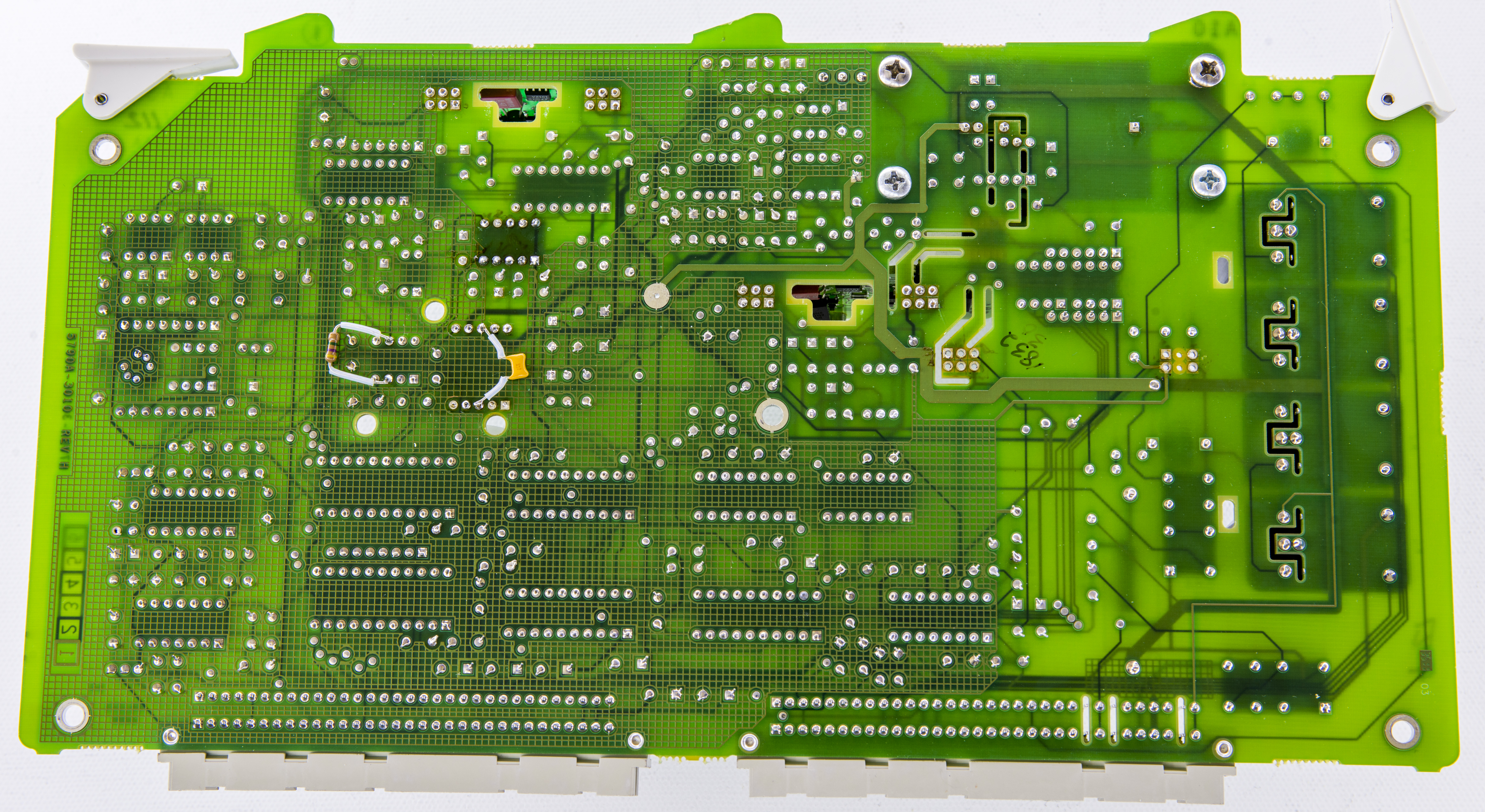
Other than few bodged up caps and resistors there is nothing else going on at the back of the PCB. Note amount of slots around critical signal nodes. PCB is 6-layer copper, as we can see by labels on left bottom side.
Another angle at the precision amplifiers, with shielding PCB and foam removed.
Protection module A92 have resistor and FET strings to protect sensitive input circuitry from sudden overvoltages.


However, Fluke 5790A is essentially a thermal transfer instrument and rely on special thermal sensor to compare unknown input signal with known internally-generated reference signal. If such sensitive detector is overloaded for long time or stressed with high-energy source then it’s input heater-detector pair may overheat and fail to open. As result no measurements would be possible with broken sensor.
Thermal sensor diagnostics
After checking all main in-guard and out-guard power supply voltages (all were good, as expected), it’s time to look at the sensor for investigation.

Fluke 5790A RMS sensor contain Beryllium Oxide ceramics. While normal use of 5790A is safe, BeO dust or fumes from damage to these component are HIGHLY TOXIC and breathing them can result in serious injury or worse. Beryllium is IARC Group 1/EPA Class A EPA carcinogen and exposure can cause Chronic Beryllium Disease, an often fatal lung disease. Never disassemble, grind, lap, fire or chemically clean RMS sensor package to avoid health hazard risks.
Key component of 5790A AC performance is the Fluke Thermal RMS Sensor (FTS) which has been proven in several products, such as 5700A/5720A and 792A. A simplified diagram of the rms sensor is shown in Figure 1. The sensor chip itself consists of two closely matched thermal voltage converters that use the temperature sensitivity of the transistor base-emitter junction in the place of the traditional thermocouple. External to the sensor chip is an error amplifier that is used to drive the second or feedback resistor/transistor pair. The output of the circuit is a dc voltage linearly proportional to the rms value of the input signal. Design requirements necessitated several modifications to the sensor and essentially pushed the sensor design to obtain the low noise, wide dynamic range, and fast settling time needed.
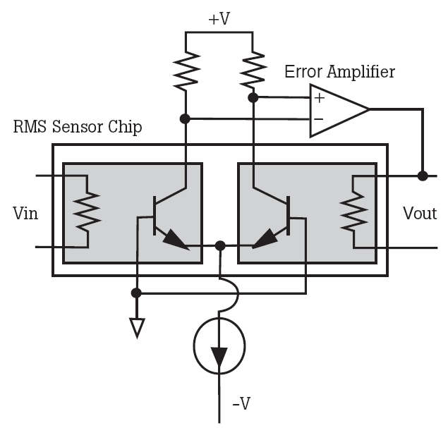
Image 75: Fluke Thermal RMS sensor. Courtesy Fluke 792A Application note
The FTS circuit converts the AC or DC signal at its input into a DC voltage equal to the RMS value of the input. The FTS consists of two identical islands suspended in air, each containing a heater resistor and an NPN transistor. Each island provides close thermal coupling between the resistor and transistor. Between islands, there is high thermal isolation. As shown in the schematic, these two transistors are connected as a differential gain stage with a differential input voltage of zero volts. Applying a voltage to the resistor on one of the islands causes that island to heat up. This in turn heats the transistor, reducing its base-emitter voltage causing an imbalance in the differential collector current. This differential current change is converted to a single-ended error current by the current mirror consisting of the two PNP transistors of U101. Op-amp U102 integrates this error current, converting it to an error voltage. The output of U102 pin 1 is then passed through a square-root circuit consisting of the other half of U102 and U103. The resultant error signal is then applied to the other side of U5 through R103, heating up that side of the sensor. When the heat on both islands of the FTS is equal, the differential error current reaches zero and the circuit is in equilibrium.
As unwanted bonus, we now take dead sensor apart to have a quick peek of it’s internal design.
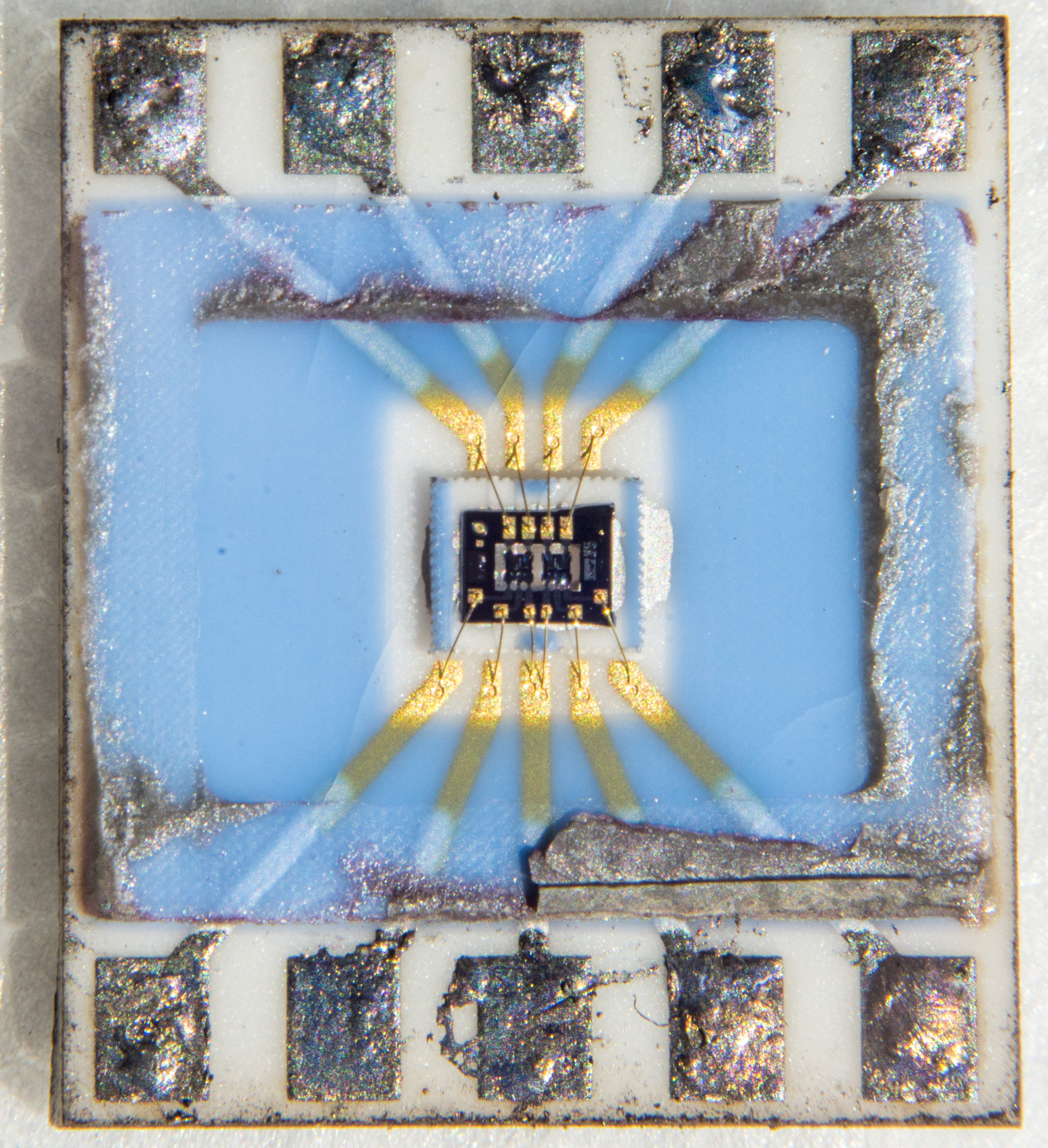

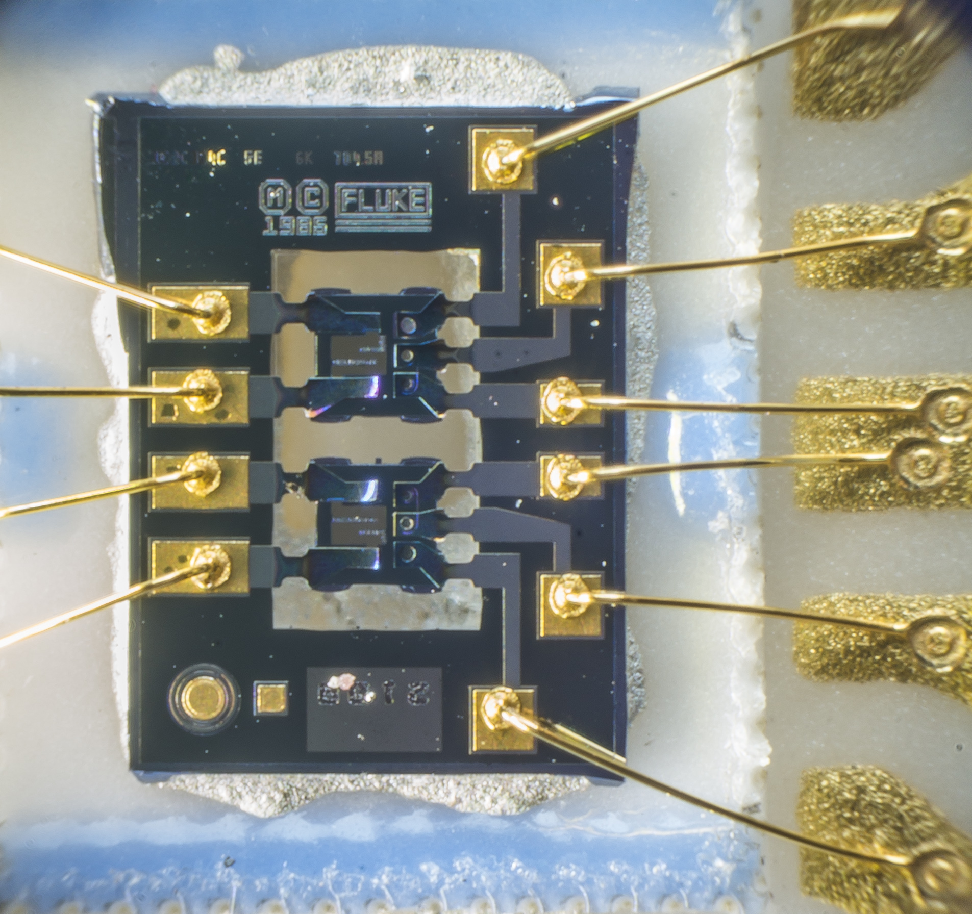
Image 76-78: Fluke Thermal Sensor hybrid chip teardown
The chip itself have original Fluke logo and have design year date 1986. Sensor chip build with three design features:
- Silicon die with input and isolated output sections.
- Small alumina interposer carrier for silicon die to decouple mechanical stress.
- Main alumina substrate with metallized traces for mechanical assembly.
An over-voltage protection circuit monitors the base-emitter voltage of the sensor transistors. As with other silicon junctions, the base-emitter junction on the FTS transistors exhibits a -2 mV/°C temperature coefficient. When the base-emitter junction falls below 200 mV, the output of U4 goes from -15 V to +15 V, turning on Q1. This shorts the sensor input to ground through the diode bridge, CR7 through CR10 and allows the FTS to cool. When the temperature falls and the base-emitter voltage increases past the 200 mV threshold, U4 again changes the state and turns off the clamp.
During a continuous overload, the protection circuit oscillates between these two states. To facilitate rapid auto ranging, the output of U4 generates an interrupt signal for the CPU by turning on Q6. This way the CPU can react quickly to an overload at the FTS.
Repair
After checking all main in-guard and out-guard power supply voltages (all were good, as expected), it’s time to look at the sensor for investigation.
Thermal sensor is dead, as it’s input resistor is >1GΩ, essentially open. Normal resistance range for Fluke Thermal Sensor is 400 Ω. Same sensor is also used in another Fluke Calibration products, such as Fluke 5700A/5720A/5730A (two sensors on AC PCBA + 1 sensor for Wideband option), Fluke 5725A booster and also Fluke 792A AC/DC Transfer Standard.
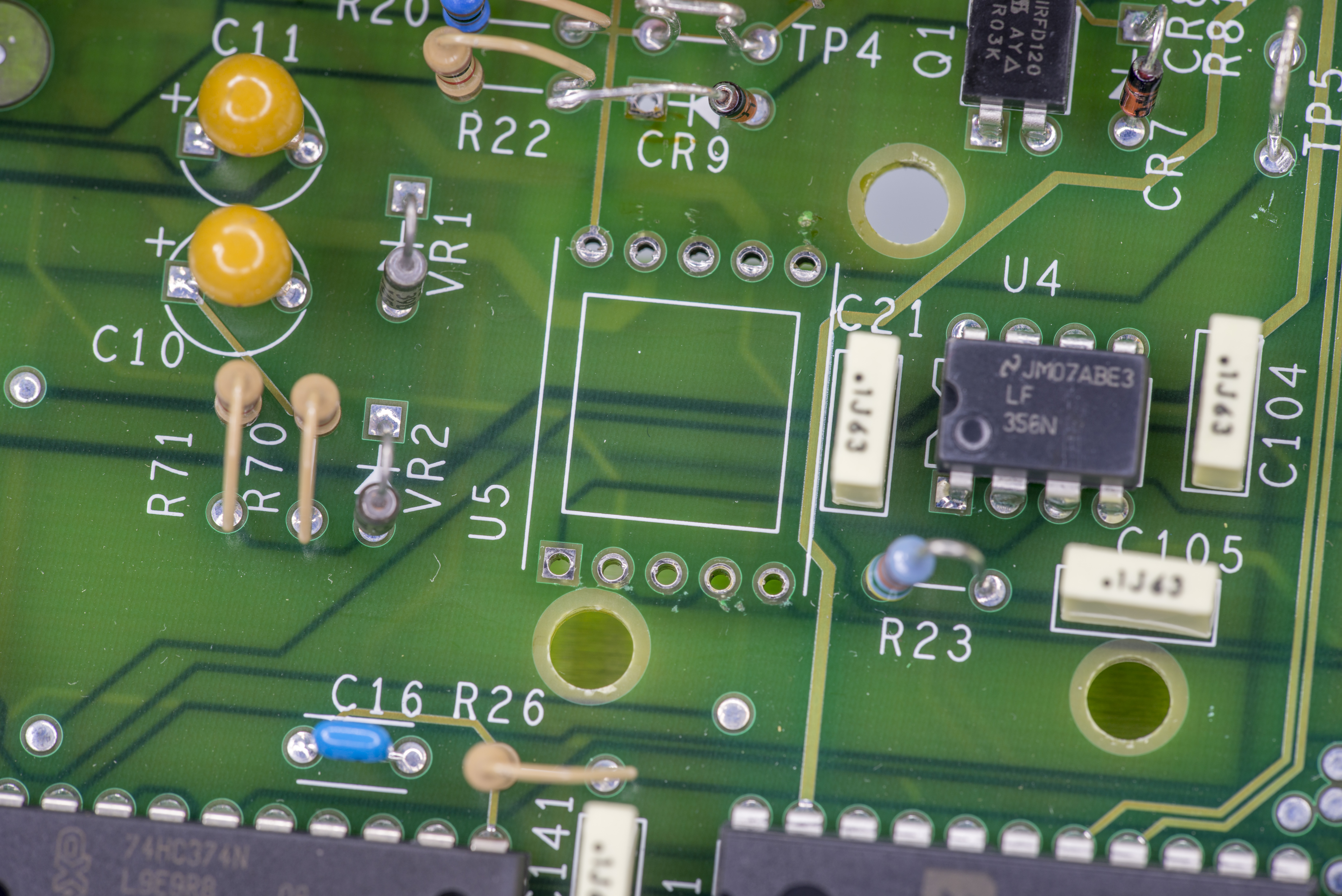
Image 79-80: Removed FTS from the board and solder blob found on A16 SIP
Strange solder bodge on A16 SIP connection was removed and cleaned up. Luckily that factory issue didn’t cause any issues, as those pins are shorted by design anyways.
So I bought used donor 5700A board A12 to salvage replacement Thermal Sensor. TRMS sensor from A12 board on the left, original now dead 5790A A10 TRMS sensor on the right.
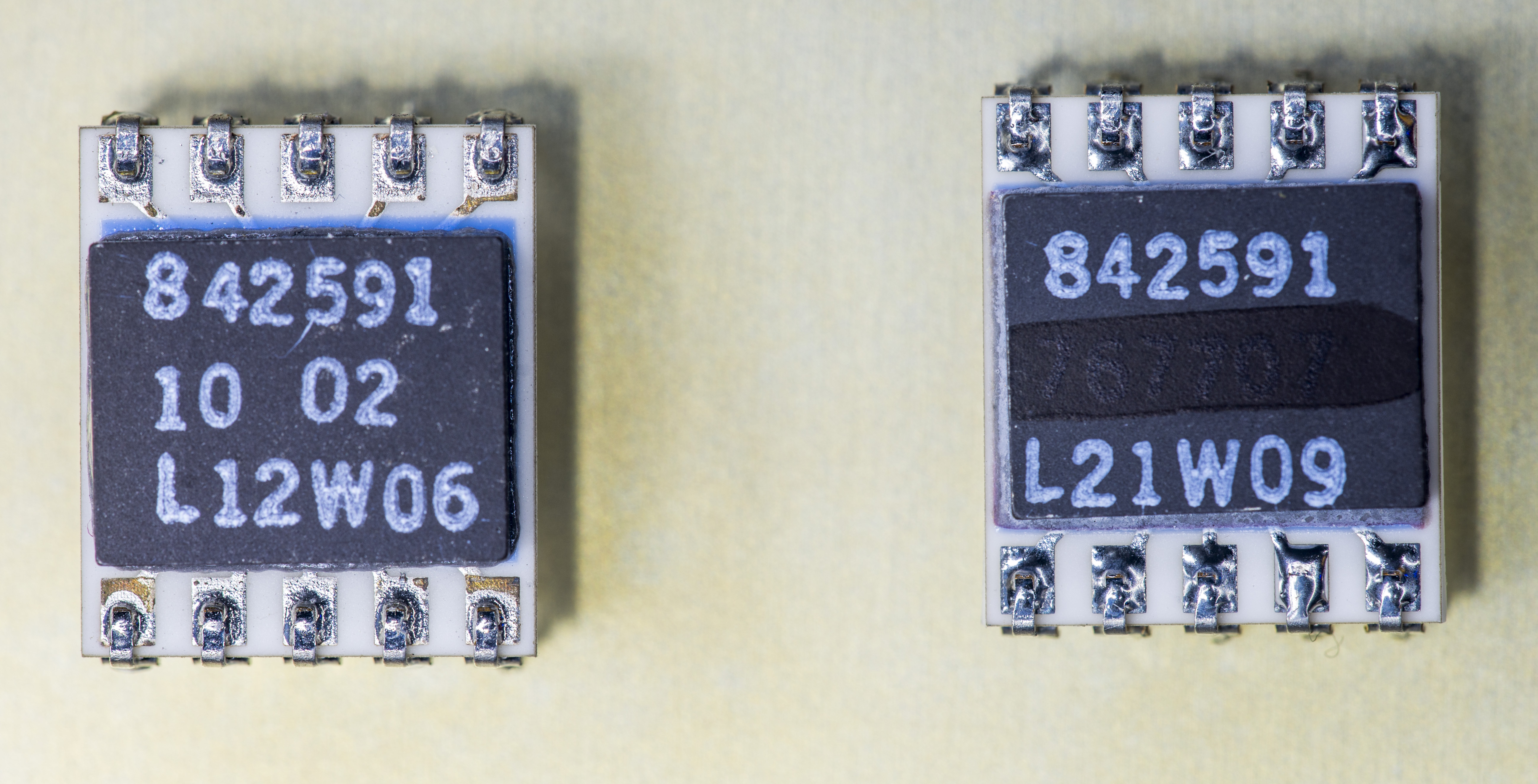
Image 81: FTS chips, good from A12 5700A left, dead from 5790A on the right
Direct input to TRMS with K7 removed:

Image 82: Testing with dummy transistors for input protection and amplifiers operation
I also had to replace some resistors around overload protection circuit used in this 5790A with values recommended by service manual. Autorange function designed in strange way, letting input signal to overload sensor. Overloaded sensor used as a trigger for processor to switch to higher range. Since by default 5790A goes to most sensitive 2.2mV range, connecting 10V AC signal (as example) will overload sensor many times in a row, while 5790A switches all the way up to 22V AC range. This does sound as a good design practice.
After chip replacement and resistor tweaking, now we can make sure everything else is fine and test the stability.
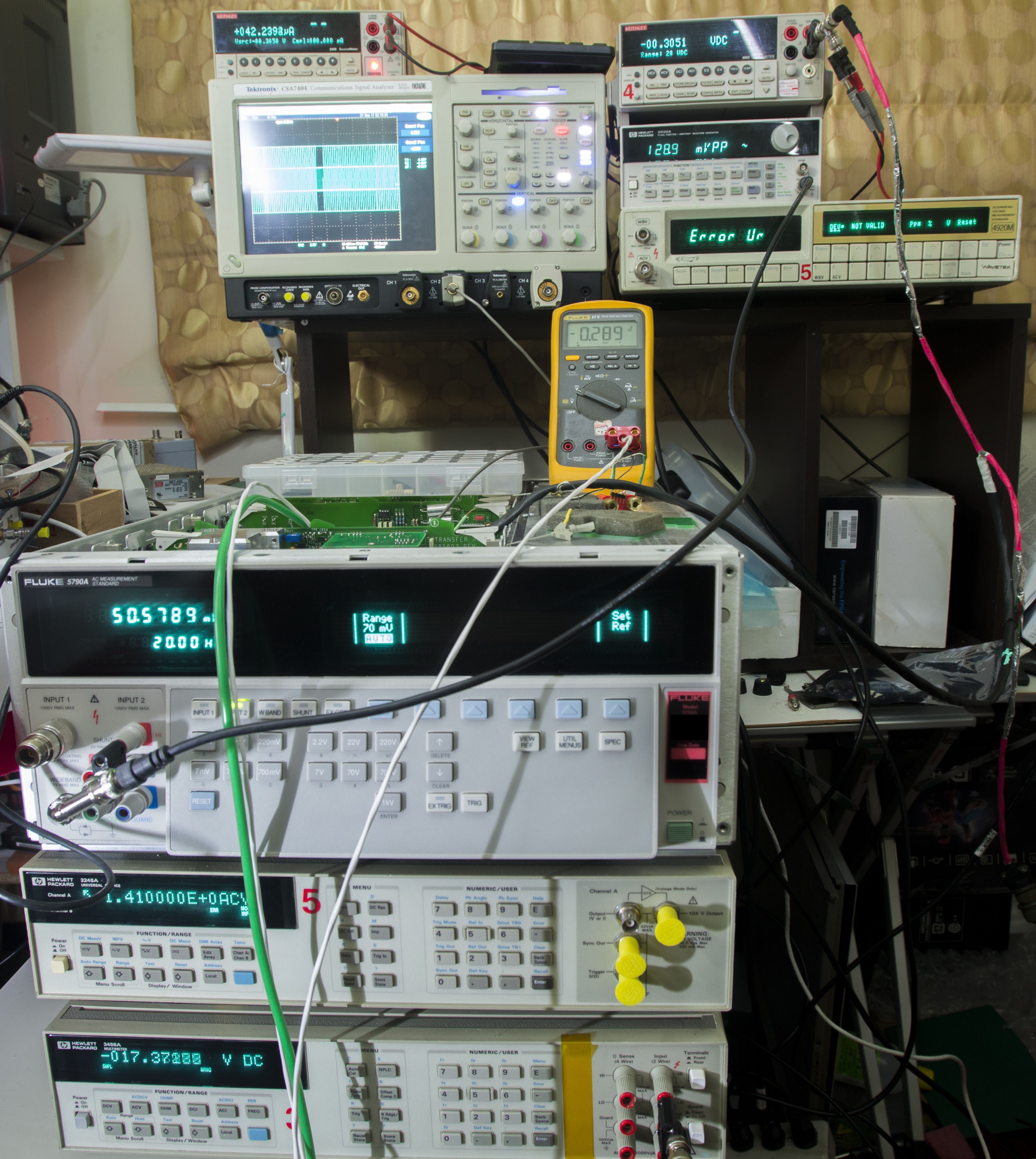
Image 84: Debug in progress, using Tektronix CSA7404 to verify signal amplitudes
Testing stability

Image 85: Comparison tests with Wavetek 4920M and HP 3458A. HP 3245A used as signal source
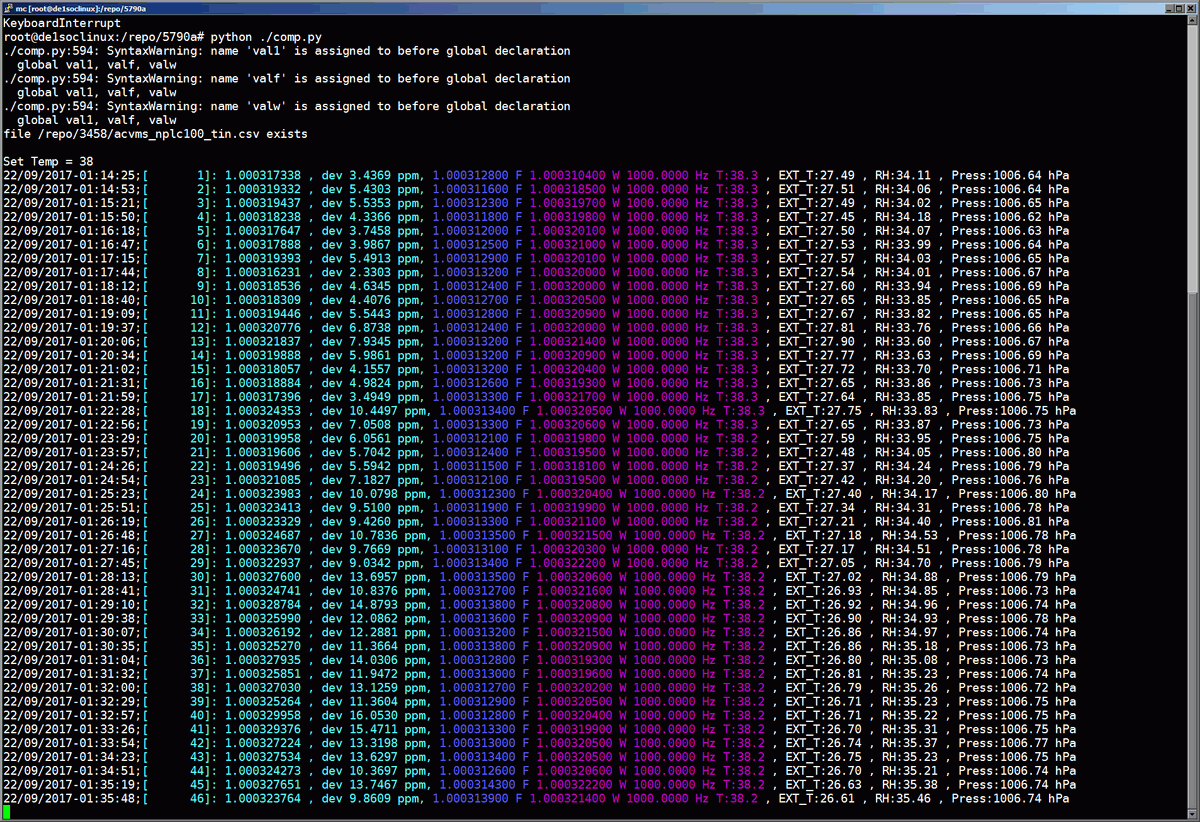
Image 86: Python app running on Raspberry Pi 3 to collect data samples over GPIB
Calibration
Interesting enough, this is the very same 5790A against which good old Wavetek 4920M was calibrated against, using Fluke 5720A as a signal source. Now after repair, that 4920M will be returning the favor for reverse calibration. This was unexpected turn.
Well, given than Fluke’s standard calibration is $5885 USD for 5790A, cost of such instrument ownership can easily exceed MSRP just after few years. Fluke acknowledge this also by providing 2 year specification limits together with more common 24 hour, 90 day and 1 year intervals. Service calibration, which is required after instrument repair or board replacements expected to cost even more. Main reference instrument to calibrate and verify 5790A’s performance is Fluke 792A, calibration of which is $4900 USD.
Periodic calibration is what you perform at the end of each calibration cycle and is all that is required to keep a normally functioning 5790A operating within specifications. For this procedure, you set the rear panel CALIBRATION MODE switch to PERIODIC. Service calibration is a more complex calibration procedure that is required only after hardware repair or replacement. Service calibration is similar to the procedure done at the factory when the 5790A is built. For this procedure, set the rear panel CALIBRATION MODE switch to SERVICE. This switch setting adds many calibration points to the software-controlled calibration routine. The CALIBRATION MODE switch setting has no effect on WIDEBAND input option calibration or verification.
Full or range Calibration
During periodic calibration of the main input, instrument is calibrated for the DC measurement function first because subsequent AC calibration relies on 5790A DC measurement accuracy. Calibrating both the DC and AC functions is part of full calibration. Also instead of full calibration, specific range calibration is possible, which presents display prompts for calibrating the DC or AC functions of a single input range. This allows to repeat portions of a just-completed calibration for fine-tuning to marching known reference signal. You can use the Skip Step softkey to redo one or a few points, leaving the rest of the calibration points unchanged.
There are three sets of calibration constants in the instrument
1. The active set. This is a volatile memory that normally contains a copy of the contents of the stored set of calibration constants. The only time it contains different data is after performed calibration of one or more ranges, but before updated constants are stored. After calibration, user must either store or discard the updated constants before resume of the normal operation.
2. The stored set. At each power up, the contents of this nonvolatile memory is copied into the active set memory. Therefore, the stored set is identical to the active set until new calibration is performed.
3. The old set. Although it is no longer in use, the previous set of calibration constants is saved in nonvolatile memory. This set is kept in order to make comparisons in Cal Shift reports.
Periodic calibration equipment requirements:
| MFC for DC test | Fluke 5700A with Rev.E or newer FW | 0-1000 VDC, short term stability <1ppm |
| DC Voltage calibrator | Fluke 5440B | 0-11 VDC, short term stability <1ppm, 1µV resolution |
| KVD | Fluke 720A | 0.1 ppm linearity |
| Reference divider | Fluke 752A | ±0.5 ppm at 100:1 or ±0.2 ppm at 10:1 |
| Null detector | Fluke 845A | 0.1 µV resolution |
| 10V standard | Fluke 732A or 732B | 10V with uncertainty ±1 ppm |
| 50 Ω N coax Tee M-M-M | Amphenol 4850 or similar | |
| 50 Ω N-F to banana | Pomona 1740 or similar | |
| Binding post to N-Male adapter | Pomona 1796 or similar | |
| Low-thermal test leads | Fluke 5440B-7002 or similar | two sets |
For AC calibration section:
| MFC | Fluke 5700A | 2mV-1000VRMS , 10Hz to 1MHz |
| Amplifier | Fluke 5725A | 220-1000VRMS, 10kHz – 100 kHz ranges |
| AC-DC Transfer Standard | Fluke 792A | 60mV – 1000 VRMS, 10Hz to 1MHz |
| 8½-digit precision DMM | HP 3458A | 0.2VDC, 10nV resolution, 0.1ppm linearity |
| 50 Ω N coax Tee M-M-M | Fluke 912605 or similar | Stainless Steel recommended |
| 50 Ω N-F to banana | Pomona 1740 or similar | |
| Frequency counter | Fluke PM6666 or HP 53131A or similar | 5 ppm uncertainty or better |
| Binding post to N-Male adapter | Pomona 1796 or similar | |
| Low-thermal test leads | Fluke 5440B-7002 or similar | two sets |
Currently xDevs.com have no ability to perform full calibration, as we lack of 5725A booster, calibrated 752A, working 845A, and our 792A is not calibrated at the moment of writing (January 2018).
However to perform basic sanity checks previously calibrated Wavetek 4920M together with calibrated HP 3458A were used:
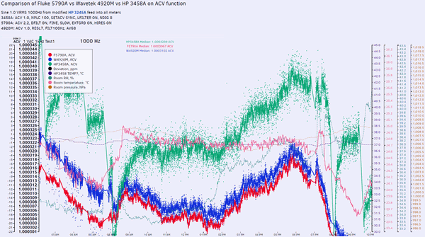
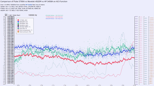
At 1 VAC 1 kHz signal Wavetek 4920M and 5790A are very close in terms of stability and noise. HP 3458A DMM provides about 3 times more noise. With 10 kHz signal frequency difference between the meters is even smaller. Note delta between Wavetek and 5790A is just 6 ppms!
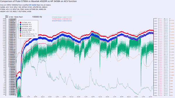
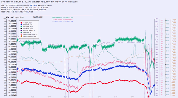
Long 2 VAC 10 kHz signal follow similar pattern, with little noisier Wavetek 4920M and much larger noise of 3458A. Jumps visible at HP meter data are result of frequent ACAL ALL routine. 10 VAC looks good too.
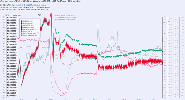
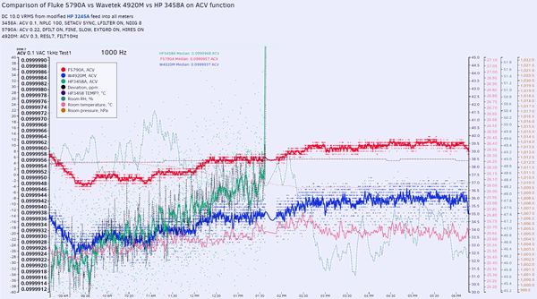
10 VDC measured by HP 3458A and Fluke 5790A reveals stronghold of 8½ HP performance, but 5790A is not too bad here, better than some other 7½ meters. Small level signal 100 mVAC 1 kHz show good performance of Fluke AVMS, multiple times less noise than the competition.
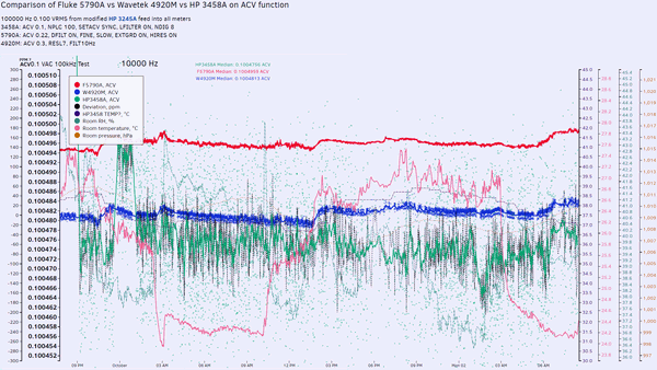
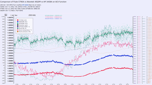
At 100 kHz frequency difference is large too. 1 VAC 250 kHz looks relatively clean on all meters.
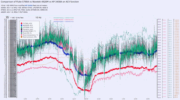
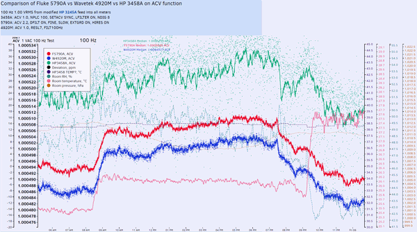
Low 10 and 100 Hz frequencies is a challenge for HP 3458A, but no problems for Wavetek 4920M and Fluke 5790A.
It’s interesting to note that even after component level repair, deviation of the uncalibrated 5790A is still relatively small versus two other instruments.
Summary and conclusion
To replace heart of the instrument, donor board was required. After multiple weeks of hunting, Fluke 5700A oscillator board was purchased, which happen to have very same Fluke Thermal RMS sensor chip (actually two of them!). This was expensive board, and there are no alternatives to it, other than sensing whole 5790A to Fluke Service Lab and paying full repair/recalibration pricetag, which likely to be many $$$$.
| Component | Cost | Shipping | Source |
|---|---|---|---|
| Fluke 5700 oscillator board for FTS donor parts | $600 USD | $75 USD | eBay |
| SD5400, LF356, DG411, LT1223, LT1227 parts, relay | $34 USD | None | Digikey, LTC, Micross |
Overall, result of such instrument overload could be much worse, for example in case of input precision divider networks damage, or ADC failure. Those circuits are custom designed and made by Fluke, and not available on market.
Now instrument still require full service level recalibration, which is costly procedure. Only few 3rd-party calibration centers can perform proper 5790A calibration to meet it’s transfer specifications.
Moral of the story is simple – do not allow overload conditions, and always double and triple check correct input signal levels BEFORE connecting to precision metrology instrument, like Fluke 5790A.
Also good idea to use 5790A only as transfer standard, to measure and calibrate another less precise meter, e.g. Fluke 8506A (which also based on thermal converter design, unlike most of traditional DMMs, including 8½ HP 3458A/Fluke 8508A) to act as a working standard.
Discussion is very welcome thru comment section or at our own IRC chat server: irc.xdevs.com (standard port 6667, channel: #xDevs.com). Web-interface for access mirrored on this page.
Projects like this are born from passion and a desire to share how things work. Education is the foundation of a healthy society - especially important in today's volatile world. xDevs began as a personal project notepad in Kherson, Ukraine back in 2008 and has grown with support of passionate readers just like you. There are no (and never will be) any ads, sponsors or shareholders behind xDevs.com, just a commitment to inspire and help learning. If you are in a position to help others like us, please consider supporting xDevs.com’s home-country Ukraine in its defense of freedom to speak, freedom to live in peace and freedom to choose their way. You can use official site to support Ukraine – United24 or Help99. Every cent counts.
Modified: Sept. 16, 2020, 1:57 a.m.