- Introduction
- Disclaimer
- Manuals references
- The arrival of the instrument
- Specifications and key features
- The challenge – HV transformer replacement
- Teardown and boards design
- The moment of truth, first power up
- Performance verification tests
- Update from February 2025, new ovenized reference board replacement copy
Intro
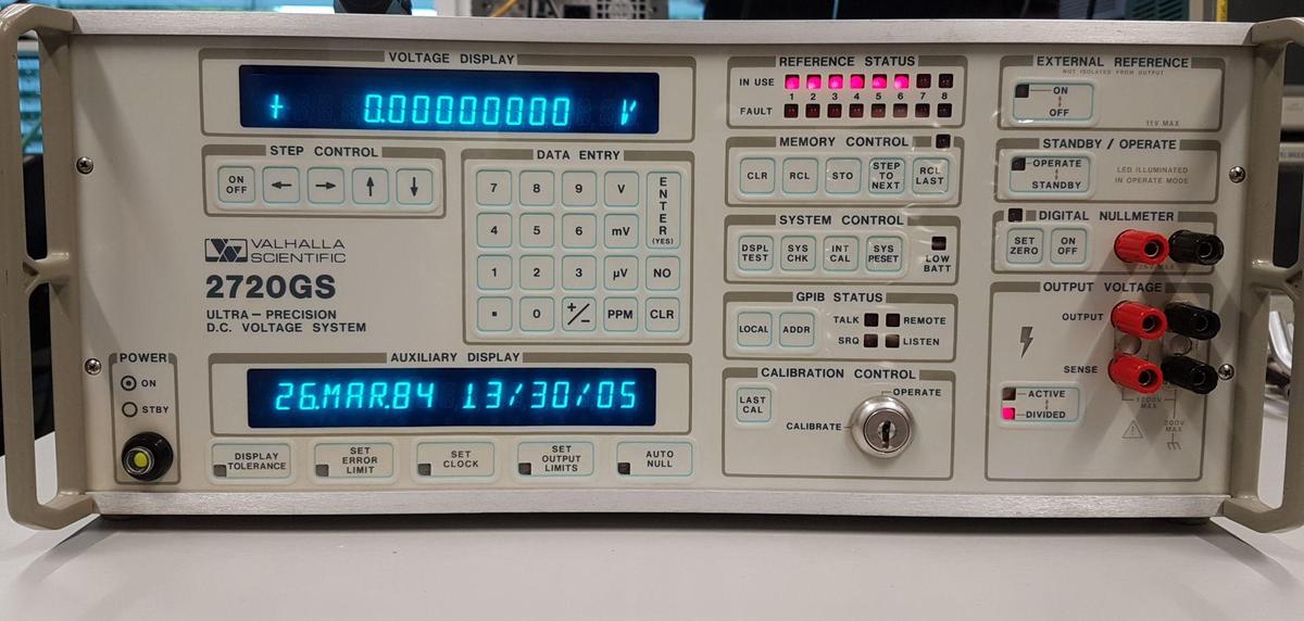
“The 2720GS Ultra-Precision Direct Voltage System” is a physical representation of Valhalla Scientific corporates philosophy, “Building New Standards for Technology”. From its fully sealed multi-function membrane control panel to its ingenious on-board multi-reference monitoring system the 2720GS is the most powerful and comprehensive direct voltage system in the world.”
These are the words that can be read in one of the descriptions about the instrument. The instrument is a Voltage calibrator, capable to calibrate 7.5 and 8.5 digit DVMs, but it also contains an on-board autoranging digital nullmeter, turning it into an 8.5-digit voltmeter at the same time and a multi-reference monitoring system, somewhat similar to what we know as Fluke 7004N/7010N.
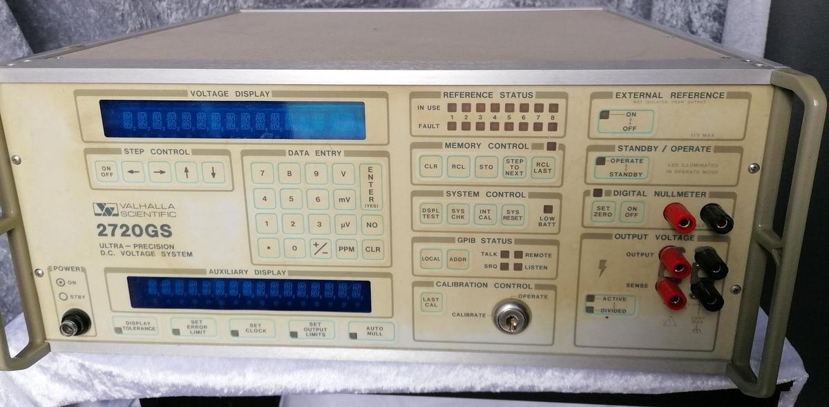
A Valhalla 2720GS was scored for a decent price, but with the drawback of a small repair story to tell.
Disclaimer
Redistribution and use of this article or any images or files referenced in it, in source and binary forms, with or without modification, are permitted provided that the following conditions are met:
- Redistribution of article must retain the above copyright notice, this list of conditions, link to this page (/fix/vh2720gs/) and the following disclaimer.
- Redistribution of files in binary form must reproduce the above copyright notice, this list of conditions, link to this page (/fix/vh2720gs/), and the following disclaimer in the documentation and/or other materials provided with the distribution, for example Readme file.
All information posted here is hosted just for education purposes and provided AS IS. In no event shall the author, xDevs.com site, or any other 3rd party, including Valhalla Scientific be liable for any special, direct, indirect, or consequential damages or any damages whatsoever resulting from loss of use, data or profits, whether in an action of contract, negligence or other tortuous action, arising out of or in connection with the use or performance of information published here.
If you willing to contribute or add your experience regarding electronics test equipment repairs or provide extra information, you can do so following these simple instructions
Manuals references
Valhalla Scientific 1989-1990 instrument catalog
Valhalla Scientific is still a company operating today, but sadly this unique 2720GS calibrator is long obsoleted and no longer supported by them.
The arrival of the instrument
The unit wasn’t directly offered but mentioned in an eBay listing of some other gear being sold. So I contacted the seller. A few days later and some mails backwards and forwards the unit was with the seller’s new location. He asked 1000€ in case the instrument is working and that he will check it first. A decent price to get my hands on it, I thought. So he tested the unit, which eventually tripped his circuit breaker and the unit released the magic smoke. That being found he offered the unit for 400€ as faulty and for parts only and I accepted without knowing what is broken.
The instrument eventually arrived and was taken apart. Some very first obvious things I noticed were blown electrolytic caps on the high voltage board, which were more than 30 years old. No surprise, I would say. So the journey started with pulling one board after the other, checking which cap values were needed and creating a list of replacement caps. This way also a totally flat AA primary lithium cell was found and some slow-blow, but blown fuses were spotted.
I made my way through the whole unit and eventually found that not only the caps on the HV power supply had thrown out their guts, but also pushed the HV transformer into Nirvana. That is some serious setback for getting the unit up and running. Following a thread on EEVBlog forum about Valhalla 2720GS this happened to others before, but no-one had a solution to that just yet. Okay, fine, we will deal with that later.
Before replacing the components the yellowed coating on the front panel was removed as good as possible with pure ethanol, just to motivate myself to work on a good looking shiny instrument.
A table with all relevant components and a link to Mouser can be found here. Notice, that also the carbon composite resistors inside the ovens were replaced, just in case.
| Board | Designator | Quantity | Specification | Populated | Size | Replacement | Size |
|---|---|---|---|---|---|---|---|
| High Voltage Power Supply | C3, C4 | 2 | 100µF, 25V, Alum radial | Mouser | |||
| C5, C6 | 2 | 10µF, 50V, Alum radial | Mouser | ||||
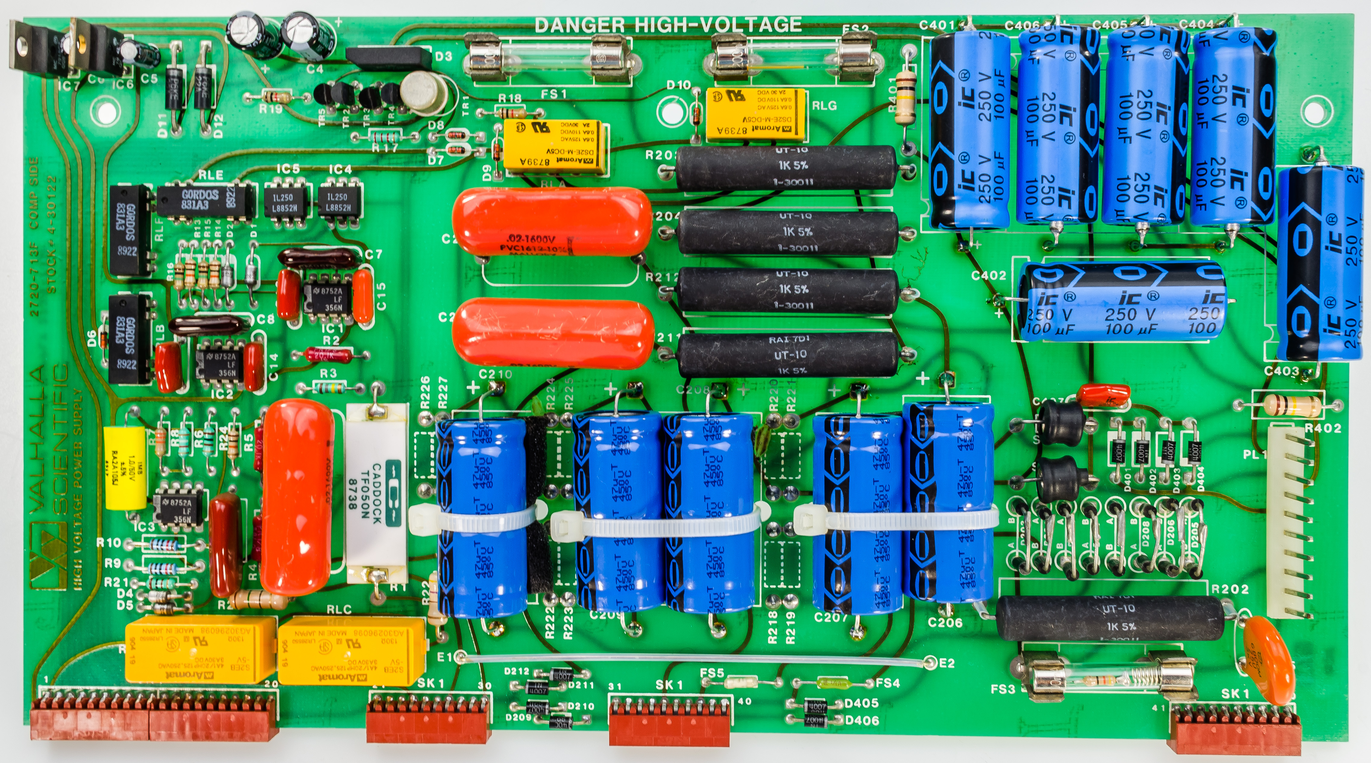
| C201-C204 | 5 | 47µF, 450V, Alum axial | 47µF, 450V, Alum axial | 18×36 | Mouser | 18 × 38 | |
| C401-C406 | 6 | 100µF, 250V, Alum axial | 100µF, 250V, Alum axial | 18×39 | Mouser | ||
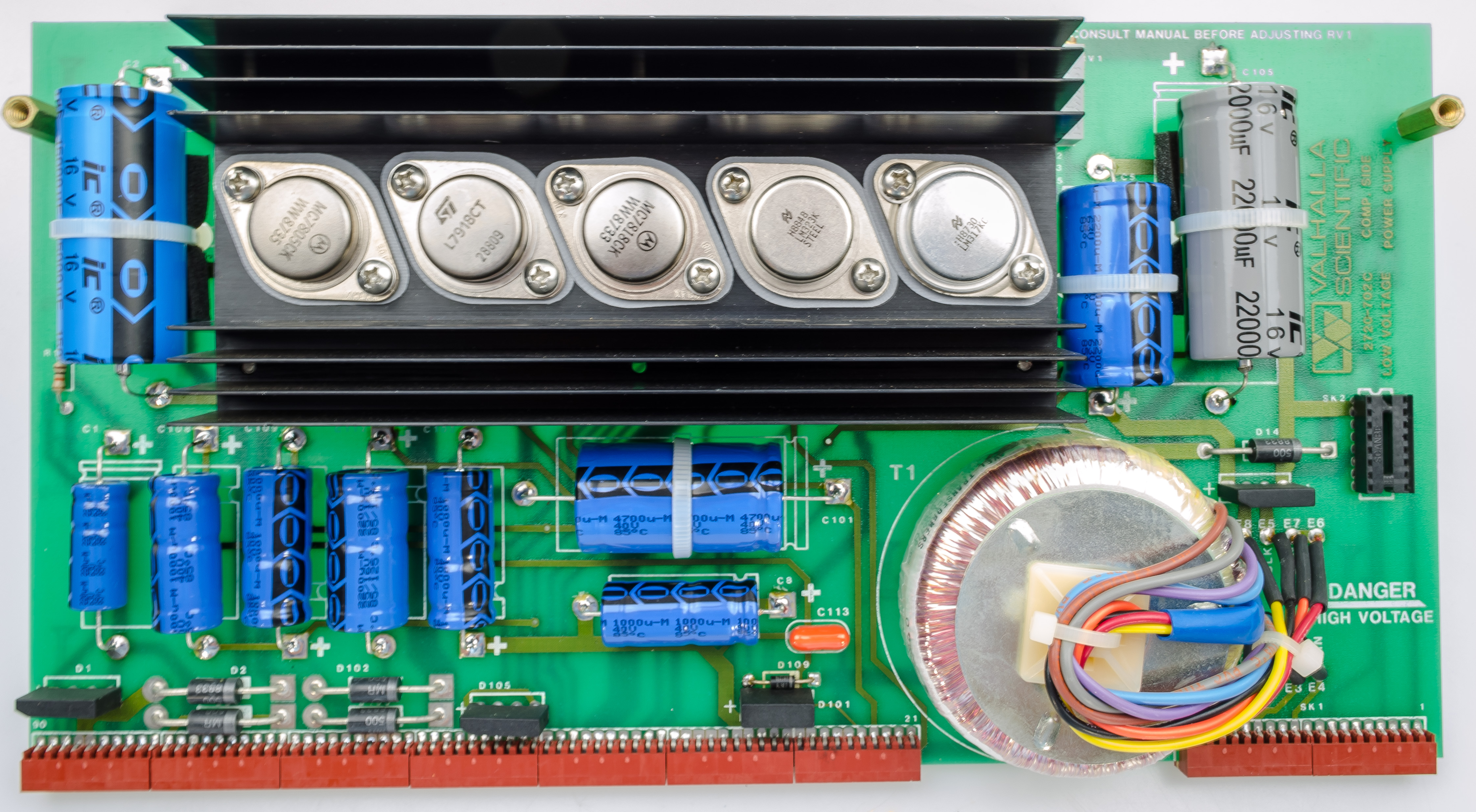
| Low Voltage Power Supply | C1 | 1 | 220µF, 63V, Alum axial | 13×25.5 | Mouser | 10×25 | |
| C2 | 1 | 15000µF, 10V Alum axial | 15000µF, 16V Alum axial | 25×50 | Mouser | 22×51 | |
| C105 | 1 | 22000µF, 10V, Alum axial | 25×61.5 | Mouser | 22×51 | ||
| C106, C3 | 2 | 100µF, 25V, Alum radial | 105 °C | Mouser | |||
| C5 | 1 | 2200µF, 35V, Alum axial | 2200µF, 50V, Alum axial | 22×40 | Mouser | 21×38 | |
| C6, C7, C103, C104, C107, C110, C111 | 7 | 10µF, 50V, Alum radial | 105 °C | Mouser | |||
| C101 | 1 | 4700µF, 35V, Alum axial | 22×50 | Mouser | 18 × 30 | ||
| C112 | 1 | 2200µF, 16V, Alum axial | 16×31 | Mouser | 15×30 | ||
| C102, C108, C109 | 3 | 1000µF, 35V, Alum axial | 12.5×31 | Mouser | 12.5×30 | ||
| C8 | 1 | 1000µF, 25V, Alum axial | 12.5×31 | Mouser | 12.5×30 | ||
| Reference Module | C4, C5, C6 | 3 | 47µF, 50V, Alum radial | Mouser | |||
| R7, R8 | 3/4× 2 | 22R, 5%, 2W, Carbon Composite | 8×17,9 | Mouser | |||
| Nullmeter | C7, C10, C104 | 3 | 100µF, 25V, Alum radial | Mouser | |||
| Main Microprocessor Board | C208, C213, C219, C224, C304, C318, C3 | 7 | 10µF, 50V, Alum radial | Mouser | |||
| C325 | 1 | 220µF, 10V, Alum radial | Mouser | ||||
| C4 | 1 | 47µF, 50V, Alum radial | Mouser | ||||
| C7, C18, C19 | 3 | 100µF, 25V, Alum radial | Mouser | ||||
| I/O Processor | C10, C101, C108 | 3 | 10µF, 50V, Alum radial | Mouser | |||
| C7, C109 | 2 | 100µF, 25V, Alum radial | Mouser | ||||
| Output System | C11, C119 | 2 | 47µF, 50V, Alum radial | Mouser | |||
| C2, C3, C7, C8, C117 | 5 | 10µF, 50V, Alum radial | Mouser | ||||
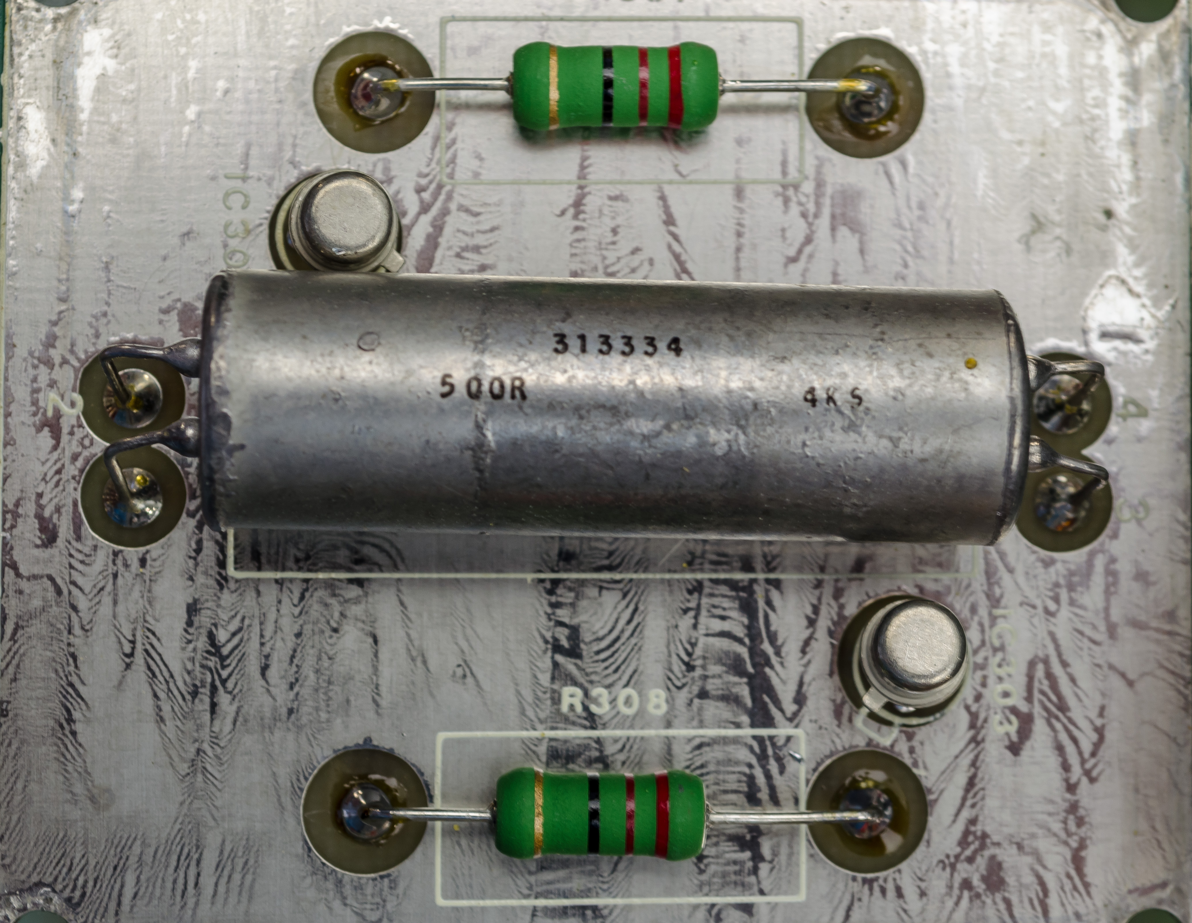
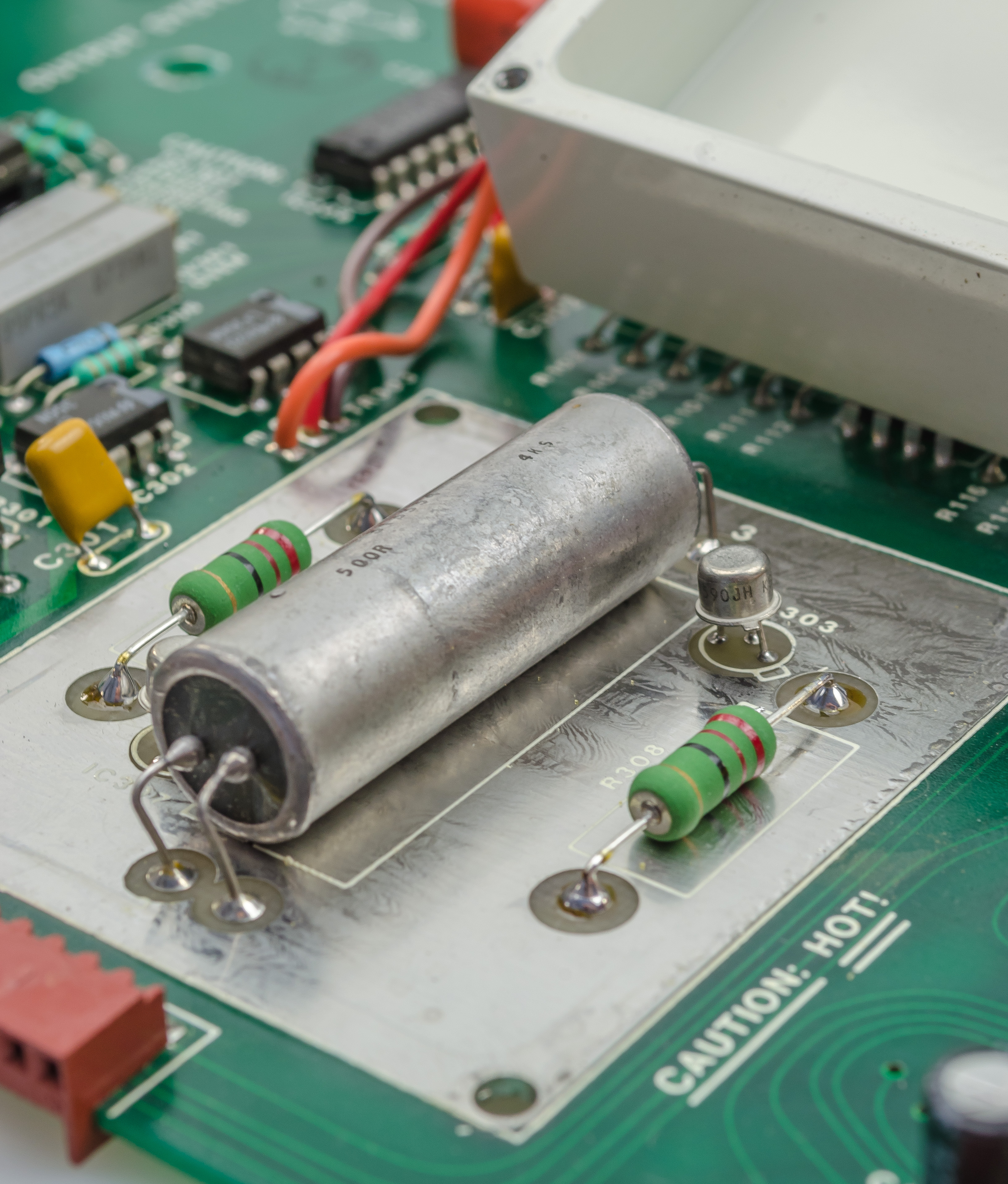
| R307, R308 | 2 | 22R, 5%, 2W, Carbon Composite | Mouser | ||||
| Front Panel | C1, C108, C4, C101, C10 | 5 | 10µF, 50V, Alum radial | Mouser | |||
| C7 | 1 | 100µF, 25V, Alum radial | Mouser | ||||
| C109 | 1 | 220µF, 16V, radial | Mouser | ||||
| HV Transformer | pri. 2× 115Vac, sec. 32Vac with center tap, 115Vac, 1100Vac | ||||||
Table: Components ordered for refurbishing 2720GS
A few days later Mouser delivered and components were swapped. Also a new lithium primary cell arrived and made its way to the frontpanel. The images below were taken after the components were replaced. The as-is images are available in the aforementioned thread, but are of less quality.
Specifications and key features
What is so special about 2720GS? First, there are three version available, 2720GS/54-4T, 2720GS and 2720HSR, which is the high-stability version. The 54-4T is a two reference boards (a total of four LM399) unit only, additionally missing the digital nullmeter, while the GS has three (a total of six LM399) and the HSR four reference boards (a total of eight LM399) inside, each reference board containing two LM399 voltage references.
Per manual these references are selected, aged and monitored for 9 to 12 months then statistically enhanced by the 2720GS’ multi-reference monitoring system. The system’s internal 30 bit A=to-D converter continually monitors each of up to eight internal highly stabilized reference zeners. Each reference module contains its own non-volatile memory which stores calibration and drift rate data. Should a reference exhibit excessive noise or drift, the system has the ability to “drop it out” and pick it up again later upon stabilization to its new value.”
“The 2720GS Direct Voltage System displays its actual or standby output voltage down to 10 nanovolt resolution or 0.01 PPM of full scale on all ranges. The extended resolution of the 2720GS is at least 10 times greater that that of the nearest competitive units. This resolution is made possible through the use of Valhalla’s proprietary 32 bit pulse-width-modulated D to A converter technology.” “The calibration of the 2720GS requires only one external instrument (a 1V/10V reference standard).”
| Range | 30 days | 90 days | 180 days | 1 year | 3 years |
| 650 mV* | 3.5 ppm + 0.2 µV | 5,5 ppm + 0.2 µV | 8.4 ppm + 0.2 µV | 13.7 ppm + 0.2 µV | 30.7 ppm + 0.2 µV |
| 1300 mV* | 3.8 ppm + 0.3 µV | 5.9 ppm + 0.3 µV | 8.7 ppm + 0.3 µV | 14.0 ppm + 0.3 µV | 31.0 ppm + 0.3 µV |
| 0.65 V | 3.5 ppm + 0.3 µV | 5.5 ppm + 0.3 µV | 8.4 ppm + 0.3 µV | 13.7 ppm + 0.3 µV | 30.7 ppm + 0.3 µV |
| 1.3 V | 3.8 ppm + 0.4 µV | 5.9 ppm + 0.4 µV | 8.7 ppm + 0.4 µV | 14.0 ppm + 0.4 µV | 31.0 ppm + 0.4 µV |
| 6.5 V | 2.8 ppm + 1.2 µV | 4.9 ppm + 1.2 µV | 7.7 ppm + 1.2 µV | 12.9 ppm + 1.2 µV | 29.0 ppm + 1.2 µV |
| 13 V | 3.2 ppm + 2.3 µV | 5.3 ppm + 2.3 µV | 8.0 ppm + 2.3 µV | 13.1 ppm + 2.3 µV | 29.2 ppm + 2.3 µV |
| 65 V | 3.8 ppm + 12 µV | 5.8 ppm + 12 µV | 8.6 ppm + 12 µV | 13.7 ppm + 12 µV | 29.7 ppm + 12 µV |
| 130 V | 4.2 ppm + 23 µV | 6.2 ppm + 23 µV | 8.9 ppm + 23 µV | 14.0 ppm + 23 µV | 30.0 ppm + 23 µV |
| 600 V | 4.5 ppm + 106 µV | 6.5 ppm + 106 µV | 9.2 ppm + 106 µV | 14.2 ppm + 106 µV | 30.3 ppm + 106 µV |
| 1200 V | 4.9 ppm + 206 µV | 6.9 ppm + 206 µV | 9.5 ppm + 206 µV | 14.5 ppm + 206 µV | 30.5 ppm + 206 µV |
Table 1: 2720GS/54-4T (ppm of setting + µV)
| Range | 30 days | 90 days | 180 days | 1 year | 3 years |
| 650 mV* | 2.3 ppm + 0.2 µV | 2.9 ppm + 0.2 µV | 3.9 ppm + 0.2 µV | 6.0 ppm + 0.2 µV | 12.6 ppm + 0.2 µV |
| 1300 mV* | 2.7 ppm + 0.3 µV | 3.3 ppm + 0.3 µV | 4.3 ppm + 0.3 µV | 6.3 ppm + 0.3 µV | 12.9 ppm + 0.3 µV |
| 0.65 V | 2.3 ppm + 0.3 µV | 2.9 ppm + 0.3 µV | 3.9 ppm + 0.3 µV | 6.0 ppm + 0.3 µV | 12.6 ppm + 0.3 µV |
| 1.3 V | 2.7 ppm + 0.4 µV | 3.3 ppm + 0.4 µV | 4.3 ppm + 0.4 µV | 6.3 ppm + 0.4 µV | 12.9 ppm + 0.4 µV |
| 6.5 V | 1.6 ppm + 1.2 µV | 2.2 ppm + 1.2 µV | 3.2 ppm + 1.2 µV | 5.0 ppm + 1.2 µV | 10.6 ppm + 1.2 µV |
| 13 V | 2.0 ppm + 2.3 µV | 2.6 ppm + 2.3 µV | 3.5 ppm + 2.3 µV | 5.3 ppm + 2.3 µV | 10.9 ppm + 2.3 µV |
| 65 V | 2.7 ppm + 12 µV | 3.3 ppm + 12 µV | 4.2 ppm + 12 µV | 5.9 ppm + 12 µV | 11.5 ppm + 12 µV |
| 130 V | 3.0 ppm + 23 µV | 3.7 ppm + 23 µV | 4.5 ppm + 23 µV | 6.2 ppm + 23 µV | 11.8 ppm + 23 µV |
| 600 V | 3.4 ppm + 106 µV | 4.0 ppm + 106 µV | 4.9 ppm + 106 µV | 6.5 ppm + 106 µV | 12.1 ppm + 106 µV |
| 1200 V | 3.8 ppm + 206 µV | 4.4 ppm + 206 µV | 5.2 ppm + 206 µV | 6.9 ppm + 206 µV | 12.4 ppm + 206 µV |
Table 2: 2720GS (ppm of setting + µV)
| Range | 30 days | 90 days | 180 days | 1 year | 3 years |
|---|---|---|---|---|---|
| 650 mV* | 2.1 ppm + 0.2 µV | 2.4 ppm + 0.2 µV | 3.0 ppm + 0.2 µV | 4.3 ppm + 0.2 µV | 8.5 ppm + 0.2 µV |
| 1300 mV* | 2.5 ppm + 0.3 µV | 2.8 ppm + 0.3 µV | 3.4 ppm + 0.3 µV | 4.6 ppm + 0.3 µV | 8.9 ppm + 0.3 µV |
| 0.65 V | 2.1 ppm + 0.3 µV | 2.4 ppm + 0.3 µV | 3.0 ppm + 0.3 µV | 4.3 ppm + 0.3 µV | 8.5 ppm + 0.3 µV |
| 1.3 V | 2.5 ppm + 0.4 µV | 2.8 ppm + 0.4 µV | 3.4 ppm + 0.4 µV | 4.6 ppm + 0.4 µV | 8.9 ppm + 0.4 µV |
| 6.5 V | 1.4 ppm + 1.2 µV | 1.7 ppm + 1.2 µV | 2.2 ppm + 1.2 µV | 3.2 ppm + 1.2 µV | 6.4 ppm + 1.2 µV |
| 13 V | 1.8 ppm + 2.3 µV | 2.1 ppm + 2.3 µV | 2.6 ppm + 2.3 µV | 3.5 ppm + 2.3 µV | 6.7 ppm + 2.3 µV |
| 65 V | 2.5 ppm + 12 µV | 2.8 ppm + 12 µV | 3.2 ppm + 12 µV | 4.2 ppm + 12 µV | 7.3 ppm + 12 µV |
| 130 V | 2.8 ppm + 23 µV | 3.2 ppm + 23 µV | 3.6 ppm + 23 µV | 4.5 ppm + 23 µV | 7.6 ppm + 23 µV |
| 600 V | 3.2 ppm + 106 µV | 3.5 ppm + 106 µV | 4.0 ppm + 106 µV | 4.9 ppm + 106 µV | 7.9 ppm + 106 µV |
| 1200 V | 3.6 ppm + 206 µV | 3.9 ppm + 206 µV | 4.3 ppm + 206 µV | 5.2 ppm + 206 µV | 8.2 ppm + 206 µV |
Table 3: 2720GS/HSR (ppm of setting + µV)
| Range | 2720GS/54-4T | 2720GS | 2720GS/HSR |
|---|---|---|---|
| 650 mV* | 0.36 ppm + 0.06 µV | 0.23 ppm + 0.06 µV | 0.19 ppm + 0.06 µV |
| 1300 mV* | 0.36 ppm + 0.1 µV | 0.23 ppm + 0.1 µV | 0.19 ppm + 0.1 µV |
| 0.65 V | 0.36 ppm + 0.2 µV | 0.23 ppm + 0.2 µV | 0.19 ppm + 0.2 µV |
| 1.3 V | 0.36 ppm + 0.3 µV | 0.23 ppm + 0.3 µV | 0.19 ppm + 0.3 µV |
| 6.5 V | 0.36 ppm + 0.6 µV | 0.23 ppm + 0.6 µV | 0.19 ppm + 0.6 µV |
| 13 V | 0.36 ppm + 1.0 µV | 0.23 ppm + 1.0 µV | 0.19 ppm + 1.0 µV |
| 65 V | 0.36 ppm + 5.4 µV | 0.23 ppm + 5.4 µV | 0.19 ppm + 5.4 µV |
| 130 V | 0.36 ppm + 10 µV | 0.23 ppm + 10 µV | 0.19 ppm + 10 µV |
| 600 V | 0.36 ppm + 50 µV | 0.23 ppm + 50 µV | 0.19 ppm + 50 µV |
| 1200 V | 0.36 ppm + 92 µV | 0.23 ppm + 92 µV | 0.19 ppm + 92 µV |
Table 4: Stability (24 h)
| Using Internal Cal | Without Use Of Internal Cal | ||||
| Range | 0-35 °C | 35-50 °C | 0-10 °C | 10-35 °C | 35-50 °C |
| 650 mV | 0.10 ppm + 0.01 µV | 0.40 ppm + 0.01 µV | 0.10 ppm + 0.01 µV | 0.10 ppm + 0.01 µV | 0.40 ppm + 0.01 µV |
| 1300 mV | 0.10 ppm + 0.02 µV | 0.40 ppm + 0.02 µV | 0.14 ppm + 0.02 µV | 0.14 ppm + 0.02 µV | 0.56 ppm + 0.02 µV |
| 0.65 V | 0.10 ppm + 0.02 µV | 0.40 ppm + 0.05 µV | 0.10 ppm + 0.02 µV | 0.10 ppm + 0.02 µV | 0.40 ppm + 0.05 µV |
| 1.3 V | 0.10 ppm + 0.02 µV | 0.40 ppm + 0.05 µV | 0.14 ppm + 0.02 µV | 0.14 ppm + 0.02 µV | 0.56 ppm + 0.05 µV |
| 6.5 V | 0.01 ppm + 0.10 µV | 0.05 ppm + 0.11 µV | 0.01 ppm + 0.10 µV | 0.01 ppm + 0.10 µV | 0.05 ppm + 0.11 µV |
| 13 V | 0.01 ppm + 0.20 µV | 0.05 ppm + 0.20 µV | 0.10 ppm + 0.20 µV | 0.10 ppm + 0.20 µV | 0.40 ppm + 0.02 µV |
| 65 V | 0.10 ppm + 1.0 µV | 0.40 ppm + 1.8 µV | 0.41 ppm + 1.0 µV | 0.22 ppm + 1.0 µV | 0.56 ppm + 1.80 µV |
| 130 V | 0.10 ppm + 2.0 µV | 0.40 ppm + 2.5 µV | 0.42 ppm + 2.0 µV | 0.24 ppm + 2.0 µV | 0.69 ppm + 2.5 µV |
| 600 V | 0.10 ppm + 9.5 µV | 0.40 ppm + 18 µV | 0.41 ppm + 9.5 µV | 0.22 ppm + 9.5 µV | 0.56 ppm + 18.0 µV |
| 1200 V | 0.10 ppm + 18.3 µV | 0.40 ppm + 24 µV | 0.42 ppm + 18.3 µV | 0.24 ppm + 18.3 µV | 0.69 ppm + 23.8 µV |
Table 5: Temperature coefficient
| Range | Resolution nV/ppm | Accuracy 90 Days (ppm of setting + µV) | Maximum Current | Wideband Noise 10 Hz to 10 kHz | Linearity |
|---|---|---|---|---|---|
| 650 mV | 10 nV/.014 ppm | 2.9 ppm + 0.27 µV | 450 ΩZ0 | 10 µV RMS | 0.14 µV |
| 1300 mV | 10 nV/.007 ppm | 3.3 ppm + 0.47 µV | 450 ΩZ0 | 10 µV RMS | 0.26 µV |
| 0.65 V | 10 nV/.014 ppm | 2.9 ppm + 0.54 µV | 100 mA | 30 µV RMS* | 0.22 µV |
| 1.3 V | 10 nV/.007 ppm | 3.3 ppm + 0.67 µV | 100 mA | 30 µV RMS* | 0.32 µV |
| 6.5 V | 10 nV/.00 2ppm | 2.2 ppm + 1.75 µV | 100 mA | 30 µV RMS* | 0.9 µV |
| 13 V | 100 nV/.007 ppm | 2.6 ppm + 3.35 µV | 100 mA | 30 µV RMS* | 1.8 µV |
| 65 V | 1 µV/.014 ppm | 3.3 ppm + 17.1 µV | 100 mA | 50 µV RMS | 10 µV |
| 130 V | 1 µV/.007 ppm | 3.7 ppm + 33 µV | 100 mA | 50 µV RMS | 18 µV |
| 600V | 10 µV/.016 ppm | 4.0 ppm + 156 µV | 30 mA | 500 µV RMS | 85 µV |
| 1200 V | 10 µV/.008 ppm | 4.4 ppm + 298 µV | 30 mA | 500 µV RMS | 165 µV |
- Add 20µV RMS for loads greater than 10mA
Table 6: Performance Characteristic Table
| Range | Resolution | Accuracy 3yr. 0-50 °C | Input Impedance |
|---|---|---|---|
| 0-200 µV | 10 nV | 0.2 % + 50 nV | >10 GΩ (1010 Ω) |
| 0.2-2 mV | 100 nV | 0.2 % + 150 nV | >100 GΩ (1011 Ω) |
| 2-20 mV | 1 µV | 0.2 % + 1 µV | >1 TΩ (1012 Ω) |
| 20-200 mV | 10 µV | 0.2 % + 10 µV | >10 TΩ (1013 Ω) |
| 0.2-2 V | 100 µV | 10 % + 1 mV | 66 MΩ nominal |
| 2-20 V | 1 mV | 10 % + 2 mV | 66 MΩ nominal |
| 20-200 V | 10 mV | 10 % + 10 mV | 66 MΩ nominal |
| 200-2000 V | 100 mV | 10 % + 100 mV | 66 MΩ nominal |
Table 7: Digital Nullmeter/Measurement Performance Table
| Range | 10 ppm | 5 ppm | 2 ppm |
|---|---|---|---|
| 1300 mV/650 mV | 500 ms | 2 s | 10 s |
| 1.3 V/.65 V | 500 ms | 2 s | 8 s |
| 13 V/65 V | 300 ms | 1 s | 5 s |
| 130 V/65 V | 600 ms | 3 s | 10 s |
| 1200 V/600 V | 800 ms | 3 s | 10 s |
Table 8: Settling Time (To within 1 PPM of final value)
“The calibration interval for the 2720GS is dependent on the accuracy the user wishes to maintain. The user should consult the accuracy tables to determine the number of days between external calibrations to obtain the required accuracy.
The recommended Internal Calibration interval is 30 days although there will be a slight gain in accuracy if this is performed at intervals down to every two days (only the “Output Gain” portion of the Internal calibration procedure need to be performed at this interval.”
While drift data are not spectacular, compared to other voltage references out there, it’s still a reasonable performance, when keeping in mind that the unit is based on LM399s. On the other hand the reference modules are averaged to create a low noise voltage reference for the A to D and the D to A converter.
“The pair of reference outputs are multiplexed onto a common “reference average” line and also onto the main A to D converter input. The reference generator section contains the main A to D converter which is used by the main µP to check the references during OBRMS cycles and during system check to check the output system, and during Internal Calibration of the 2720GS. This section also contains a buffer amplifier to supply the main D to A converter with the average reference voltage. The Main Digital to Analog Converter provides an extremely linear output voltage controlled by digital data from the main µP and referenced to the reference supplied by the reference generator. The relay Polarity Selection provides polarity switching at the output of the main D to A converter. The Error Amplifier compares the output of the D to A converter (via the polarity selection) and the main attenuator output, thus maintaining the voltage at the sense terminals (divided or amplified as required) at a fixed relationship to the output of the D to A converter.”
Additionally, with the external reference input options (EXR1 = 1 V, EXR7 = 7 V, EXR10 = 10 V) the internal reference drift can be overcome.
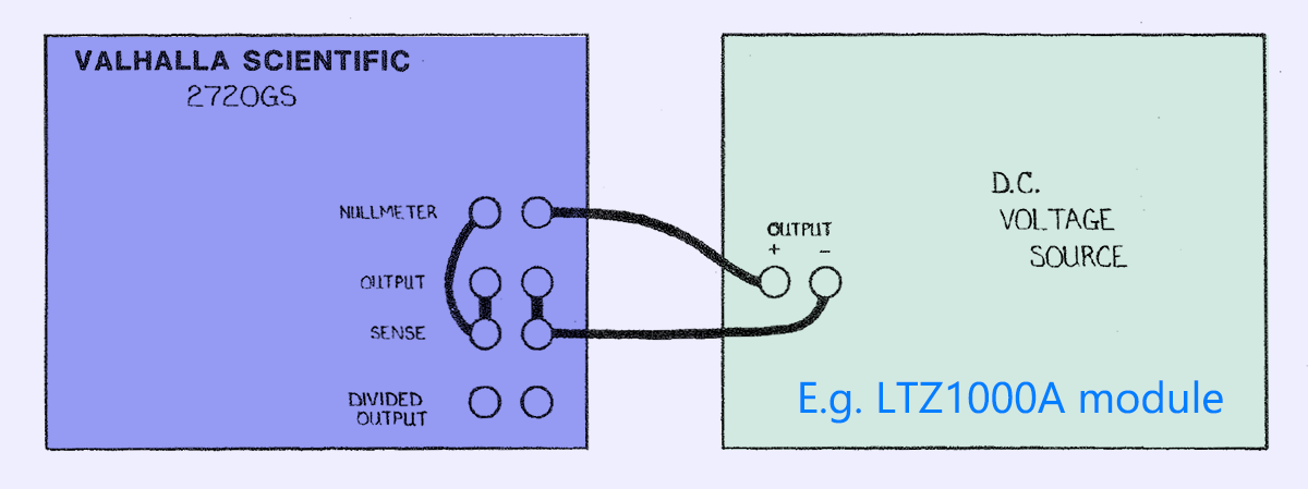
The challenge – HV transformer replacement
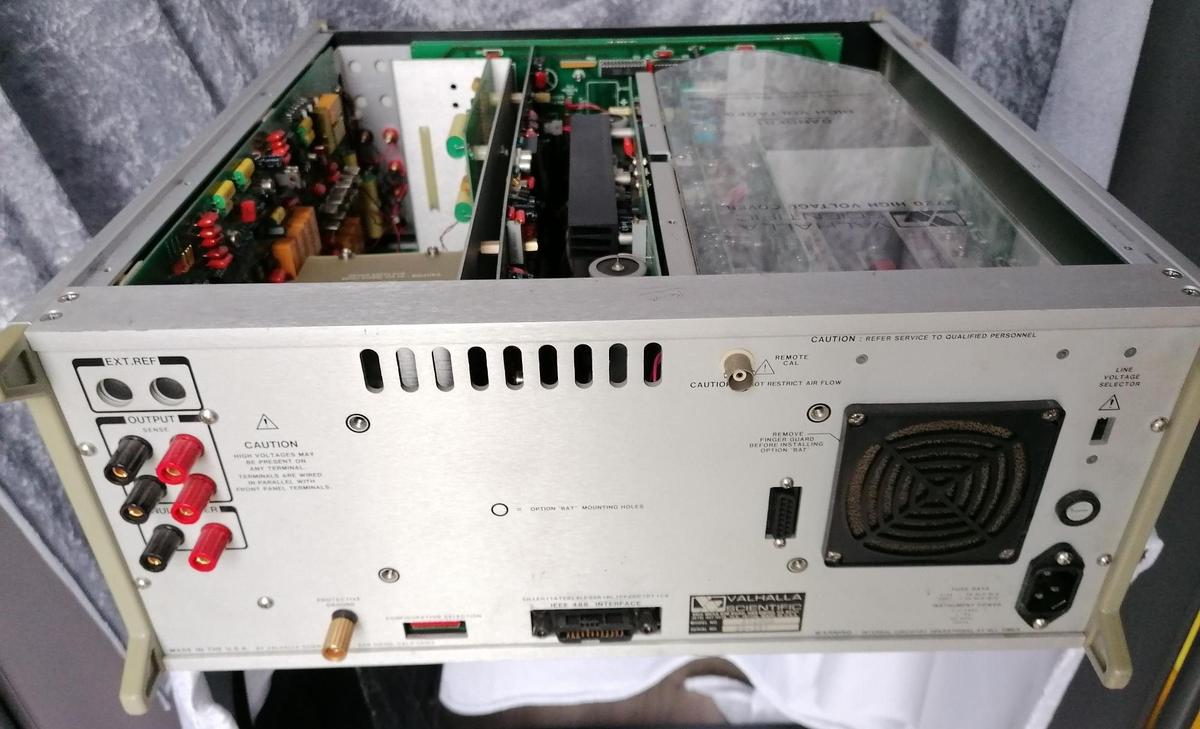
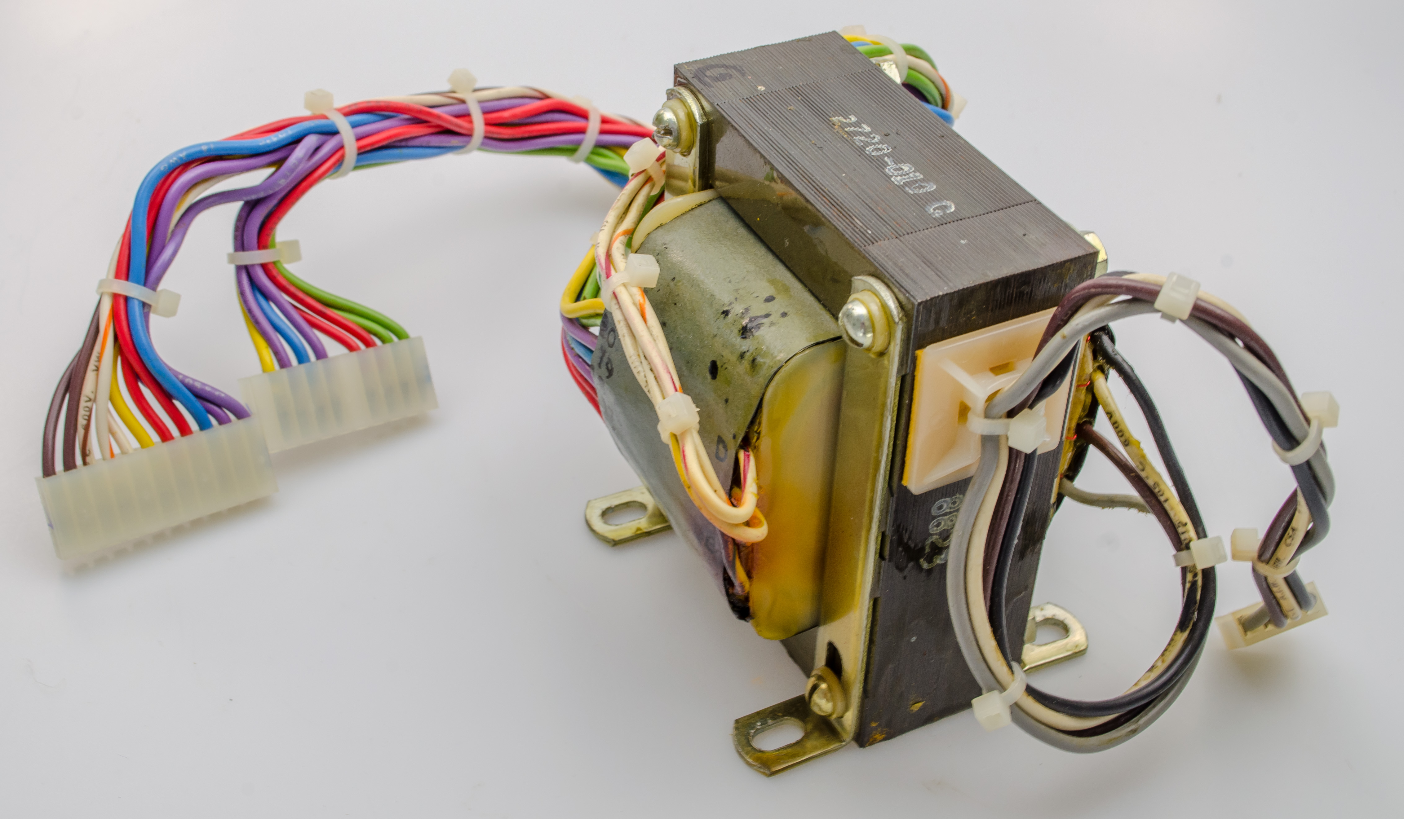
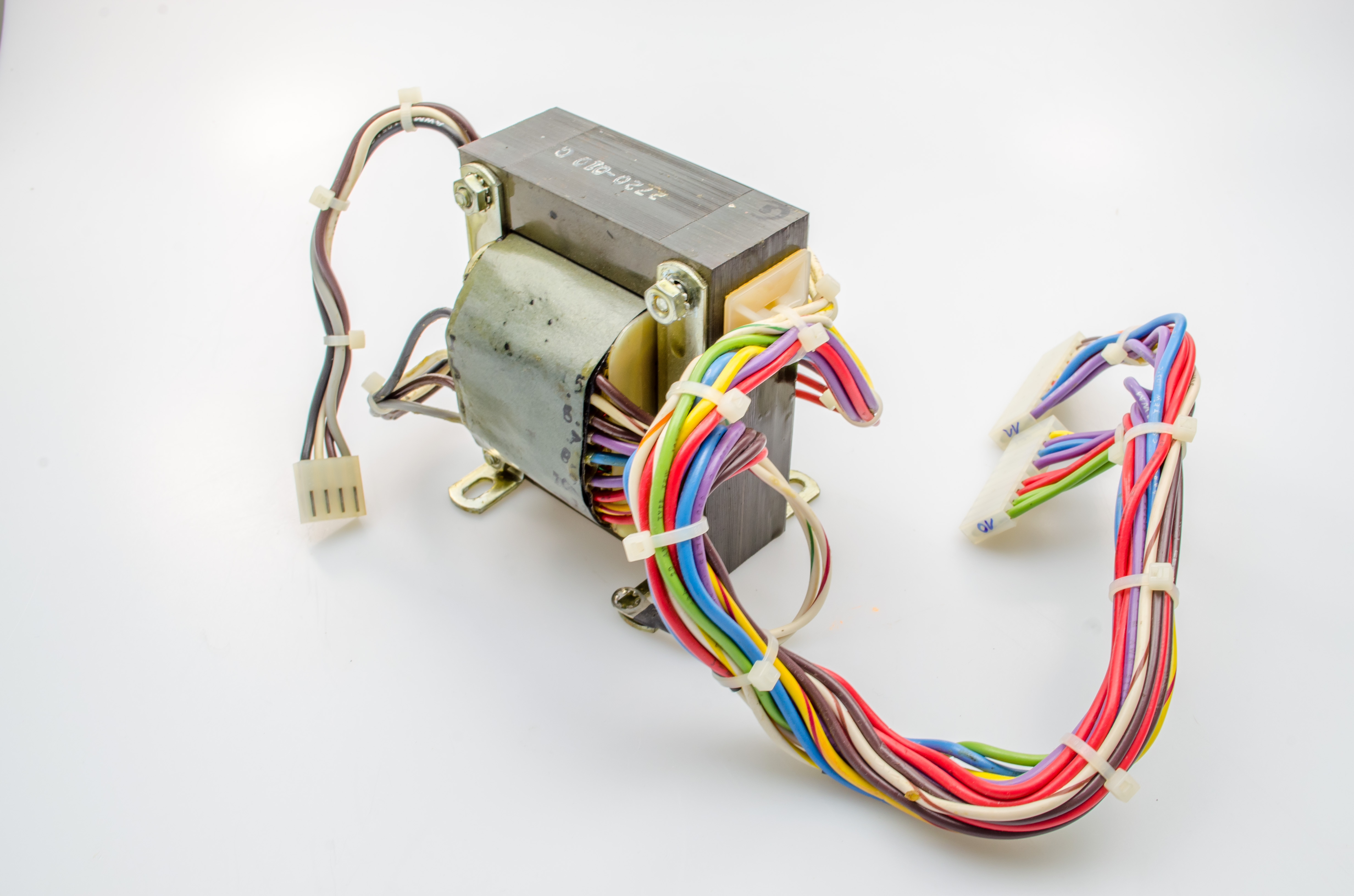
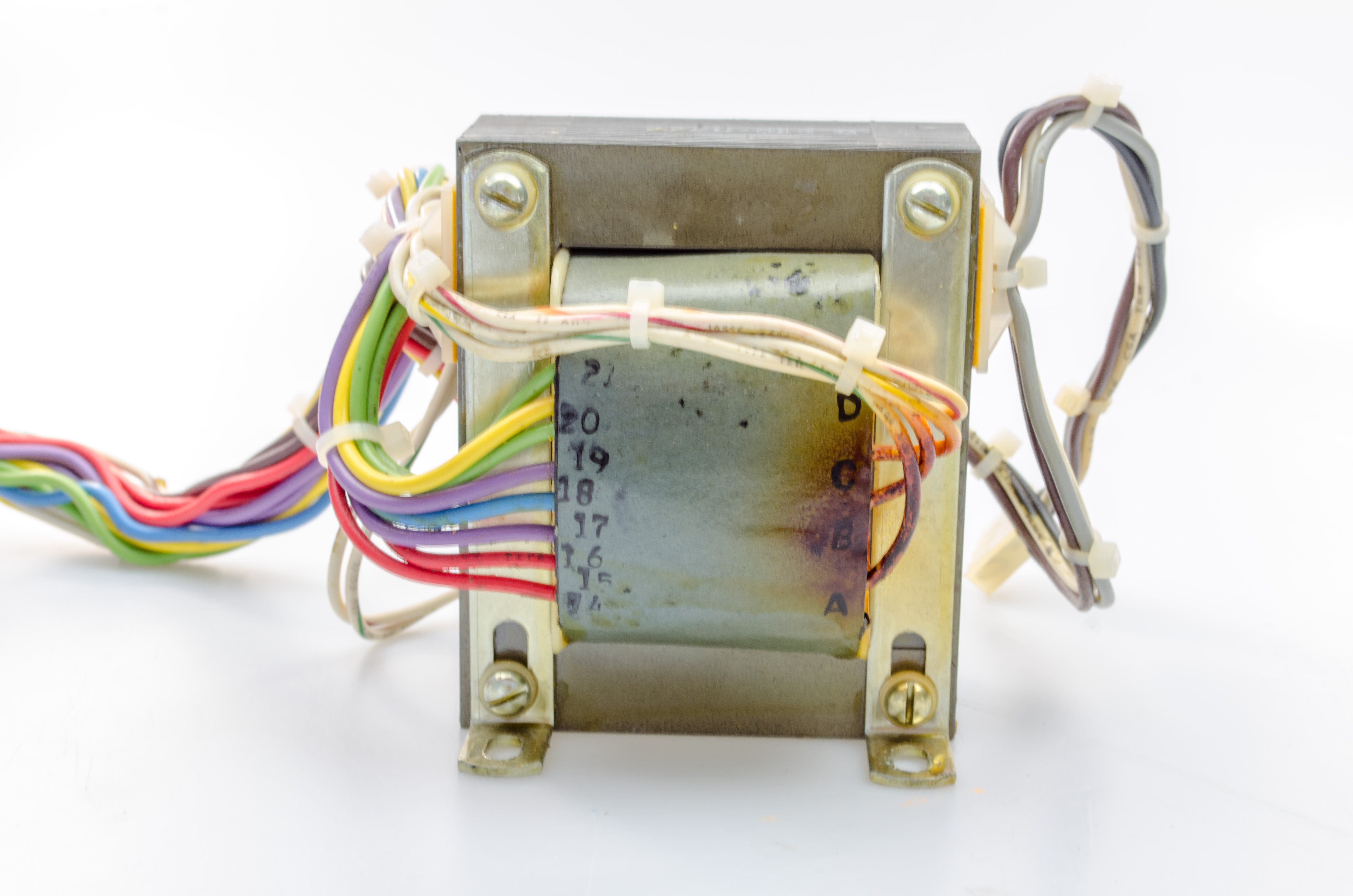
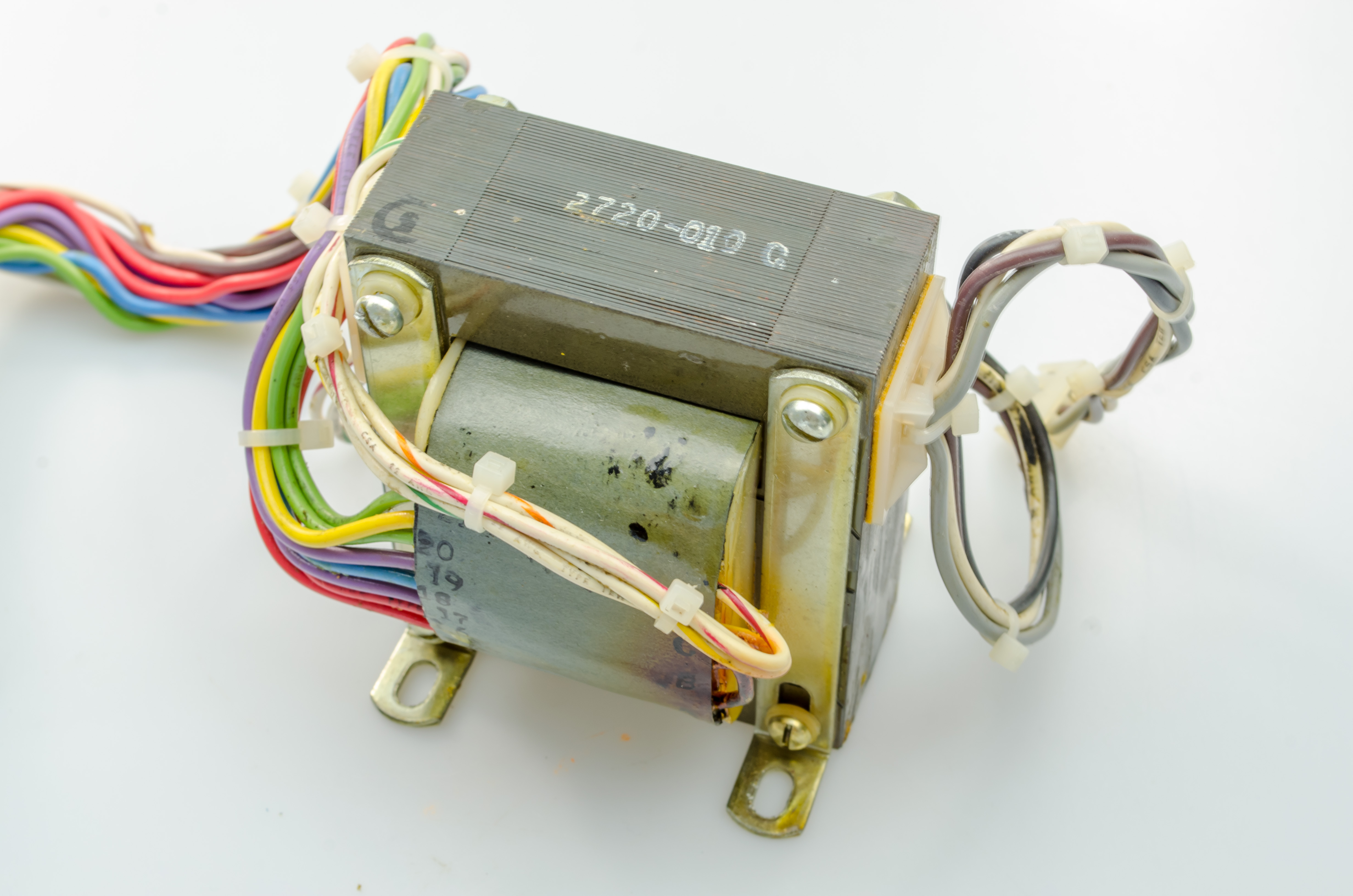
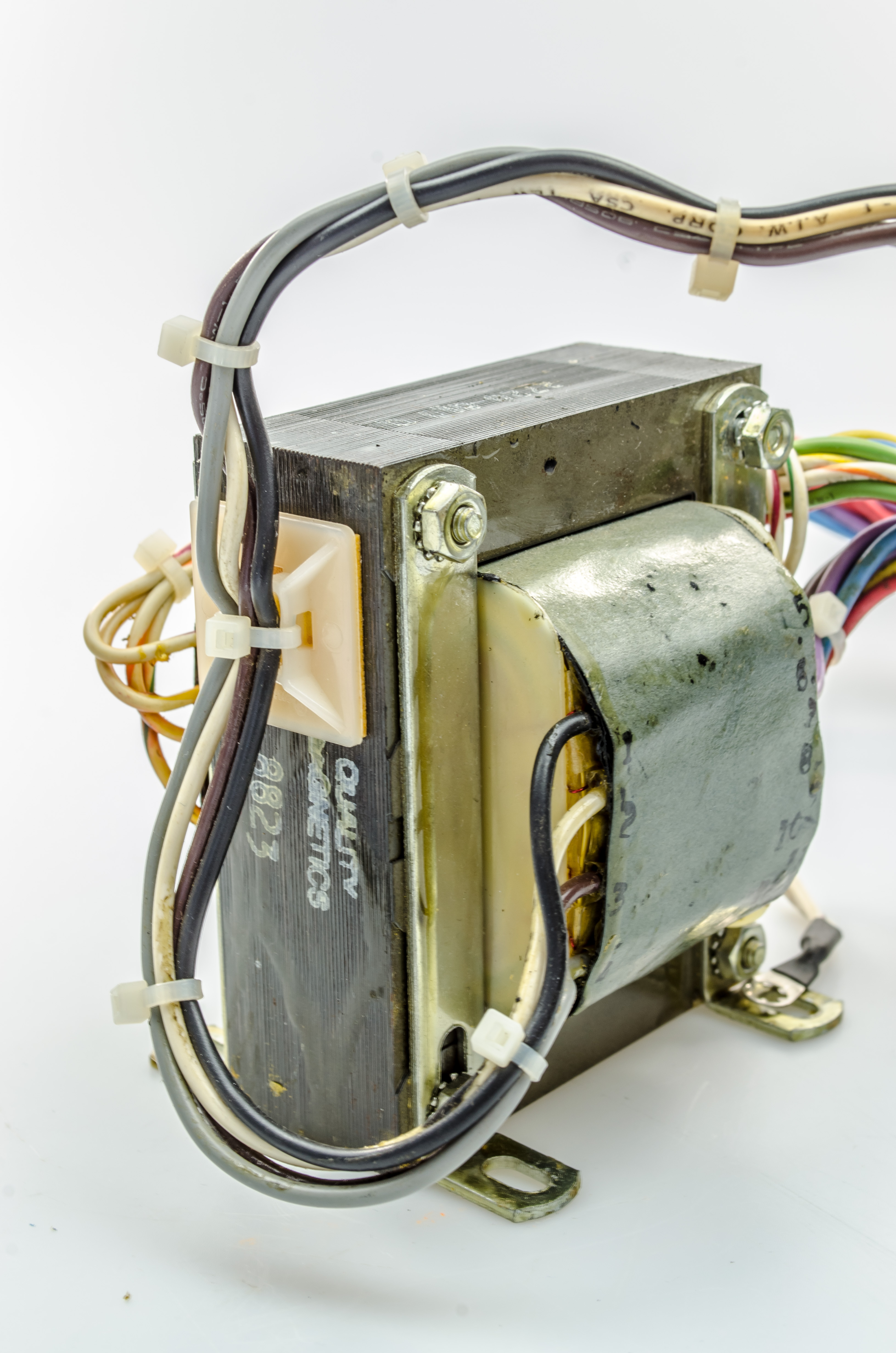
A replacement was needed for the HV transformer in order to get the unit up and running. This transformer features a 2× 115 Vac input, a 32 Vac with center tap, an 115 Vac to the same center tap and an 1100 Vac output. There are also some screens involved, one that is between primary and 1100 Vac and connected to the core and two between the other secondaries, that are connected to E9 and E10 on the Mother Board Assembly.
![]()
Several companies were contacted and asked for offers. Beside some companies rejecting any offer at all, some others were offering analysis and rewinding for prices ranging from a minimum of 500€ up to more than 1400€ plus copper plus VAT. Way too much and way beyond economical repair for one off instrument project.
Fortunately, a company named Wickeltechnik Langer was found and offered analysis and a copy of the transformer for a reasonable price. Furthermore, they had left a palett with the correct EI core metal sheets to recreate the original dimensions 90 mm x 80 mm (x 33mm), perfect.
![]()
A group order was arranged to share analysis costs and help ‘em all with a working custom made replacement, so eventually the order was placed.
A first sample arrived within a week and was checked, but turned out to be not as expected. Some quick phone calls later and the company was ready for a second try. The new sample arrived again within a week and turned out to be exactly what was needed as a replacement. Lucky enough, the old cables were rescued and reused for it, so no new connectors had to be configured.
So if you are in the need of a replacement HV-transformer, Wickeltechnik Langer is your contact to get it.
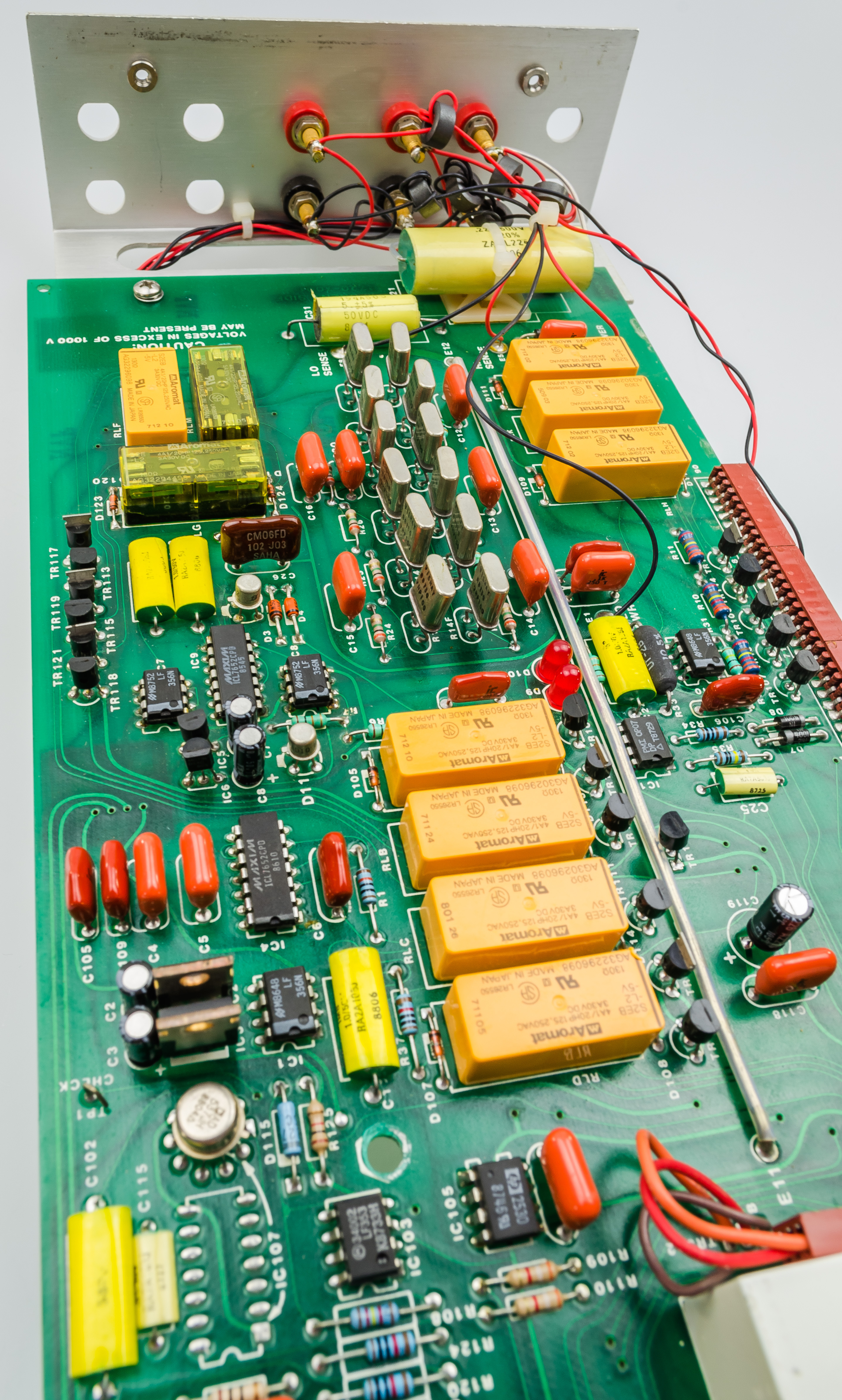
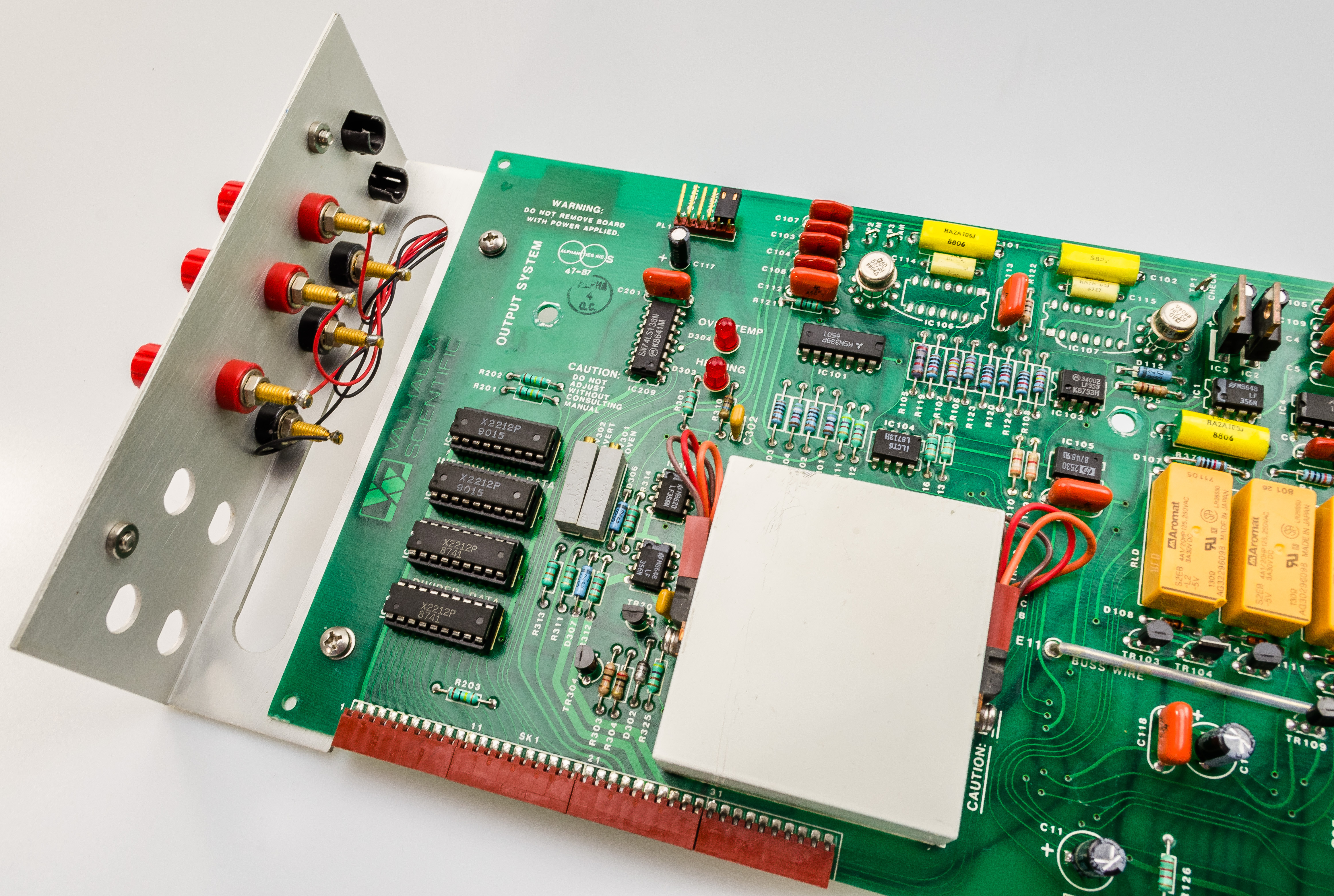
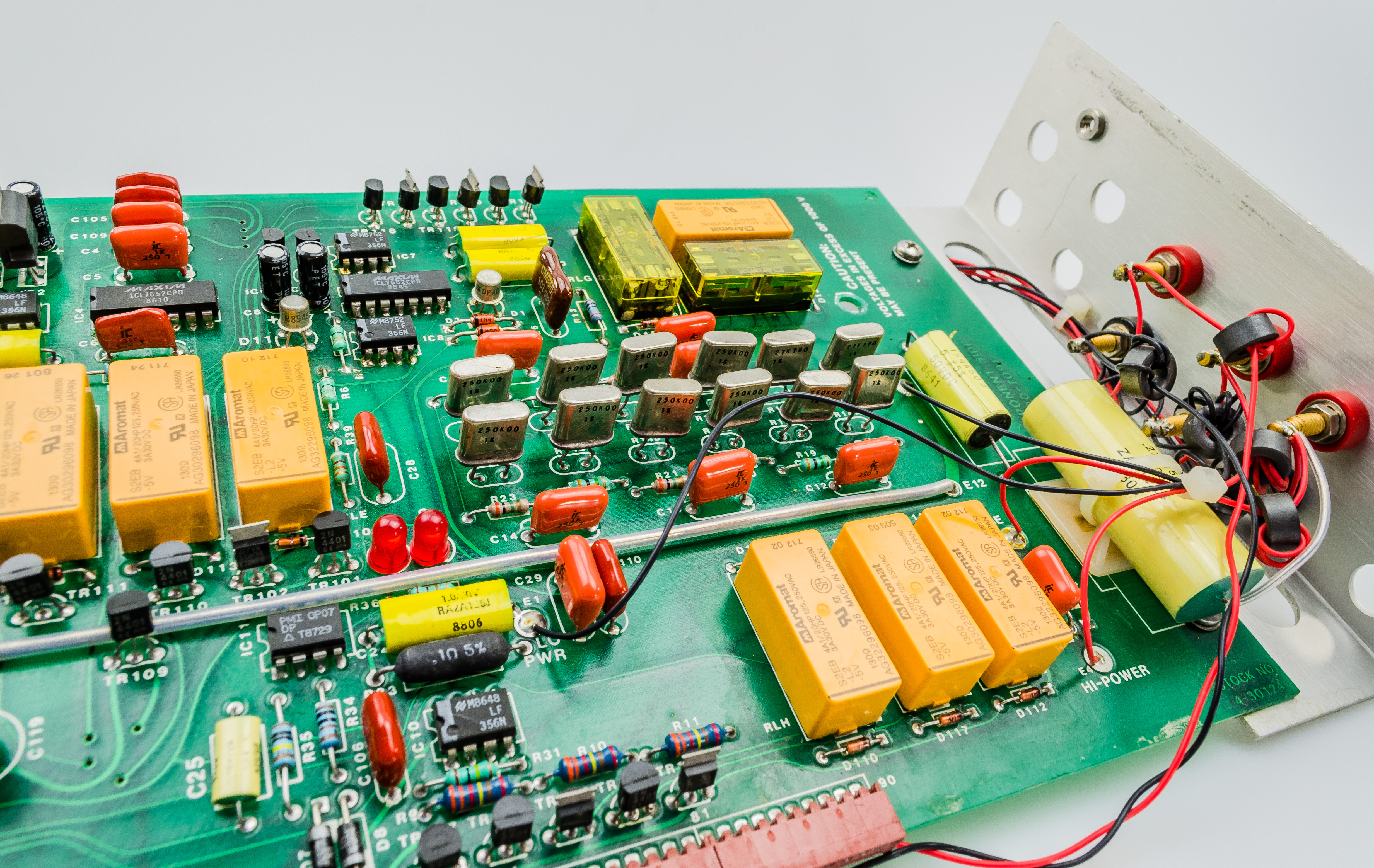
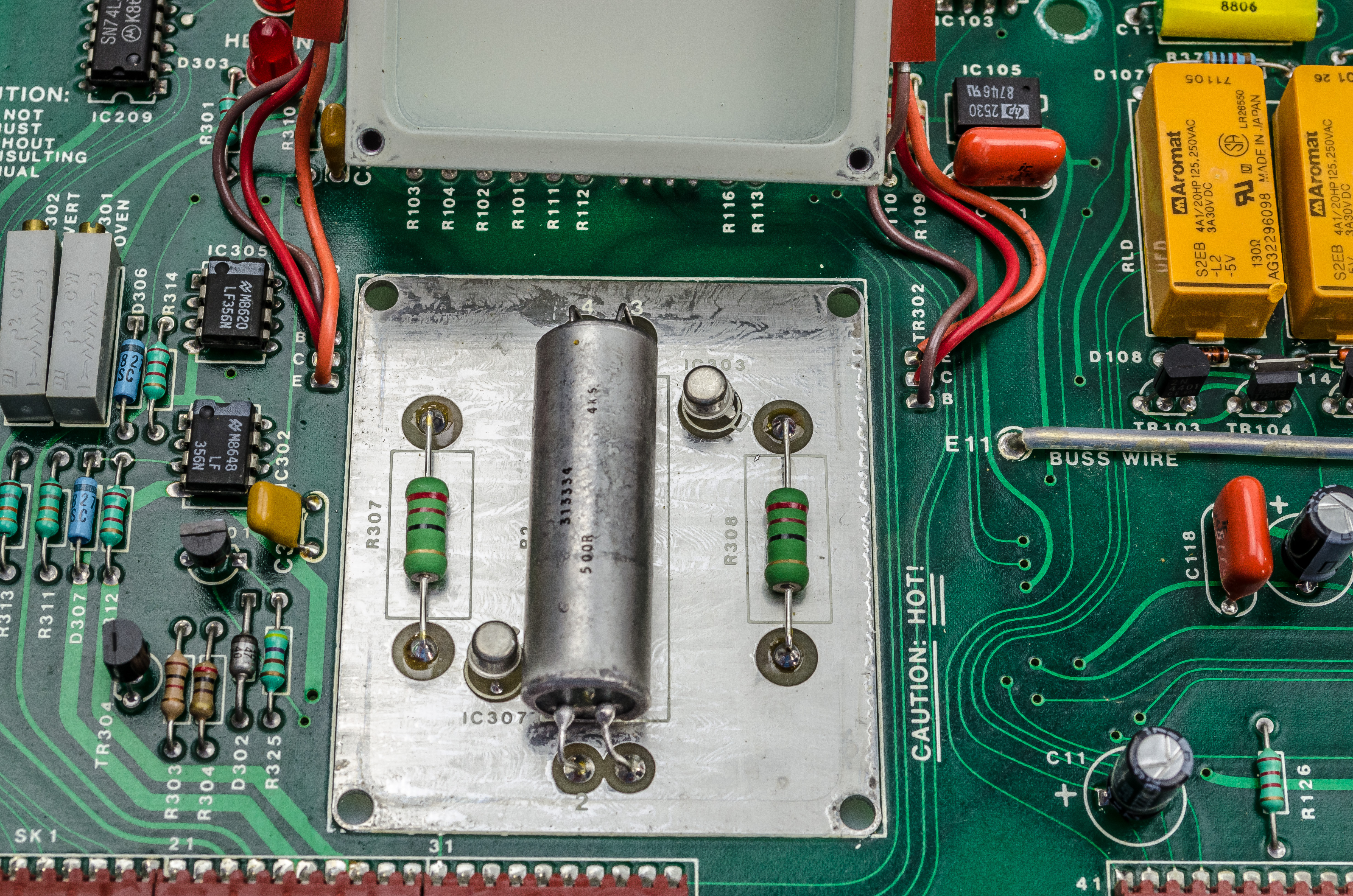
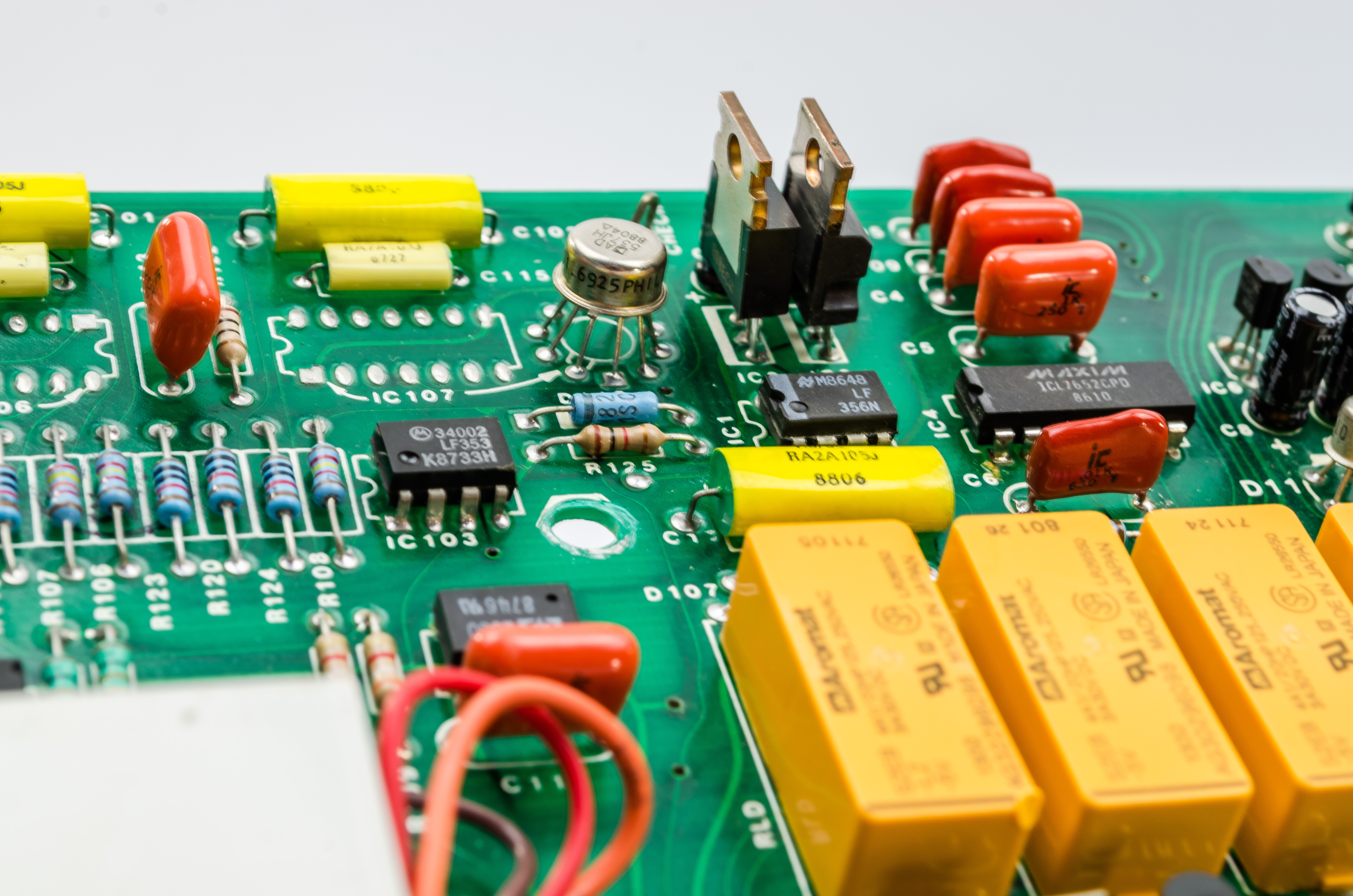
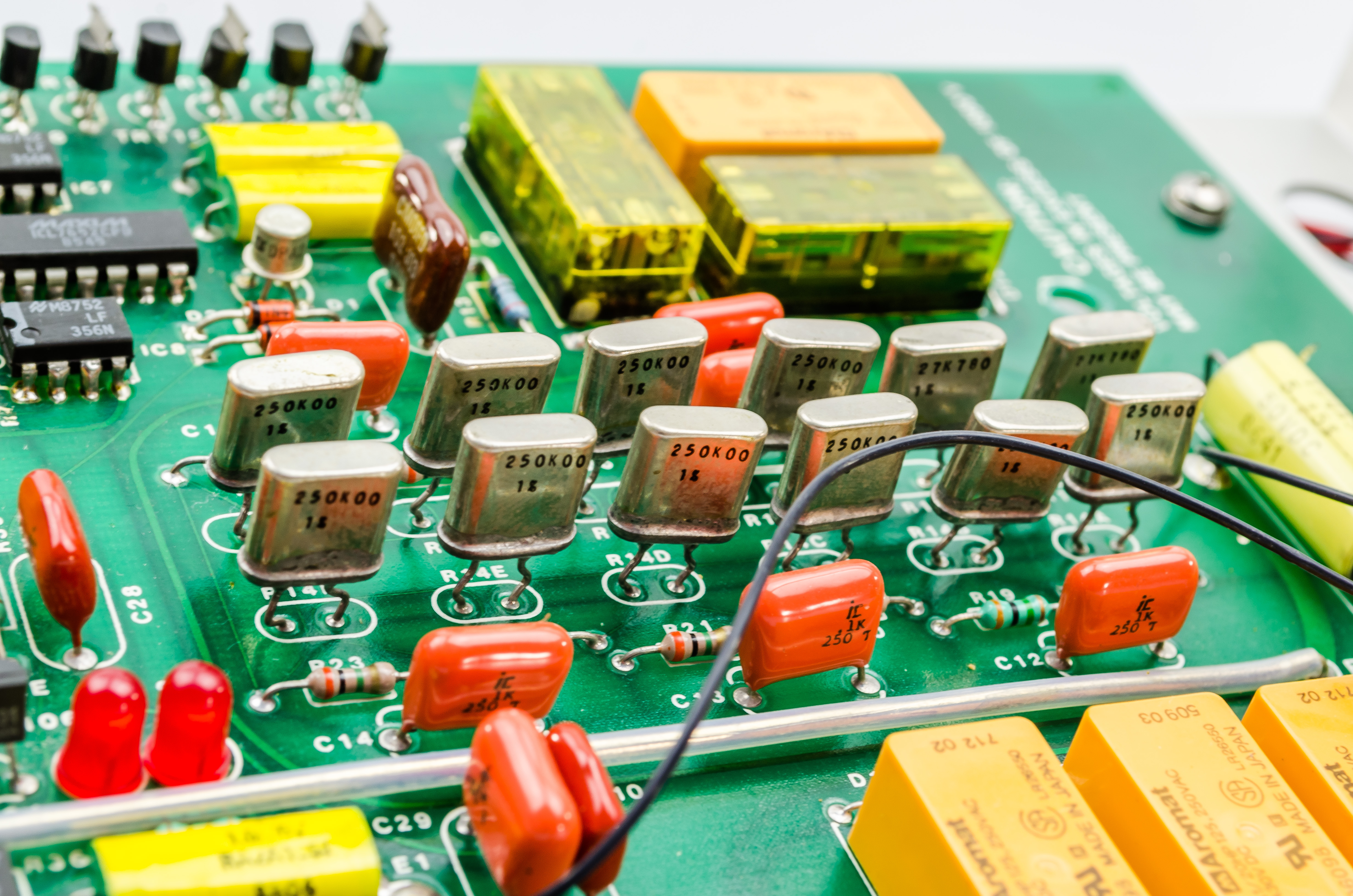
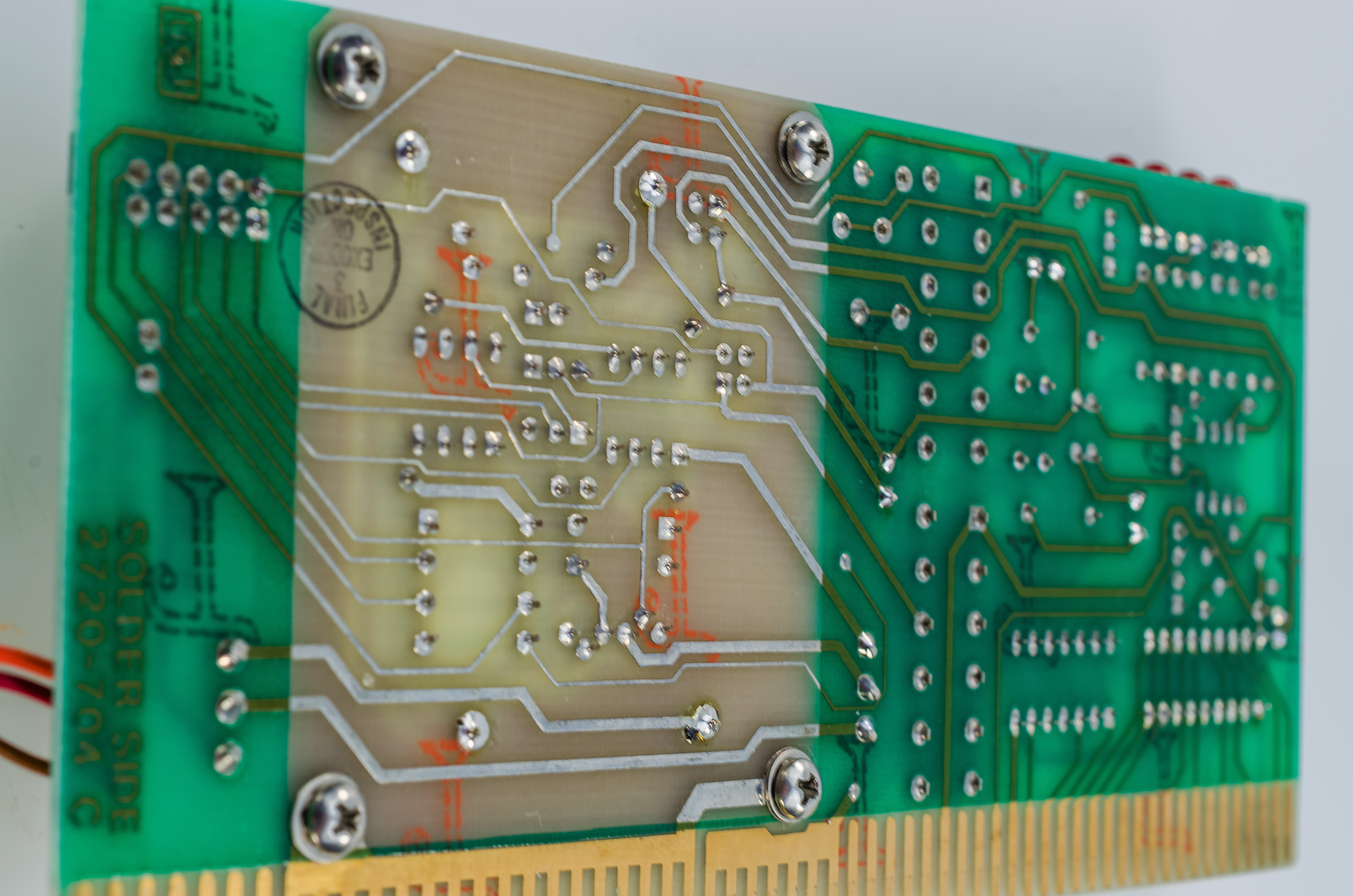
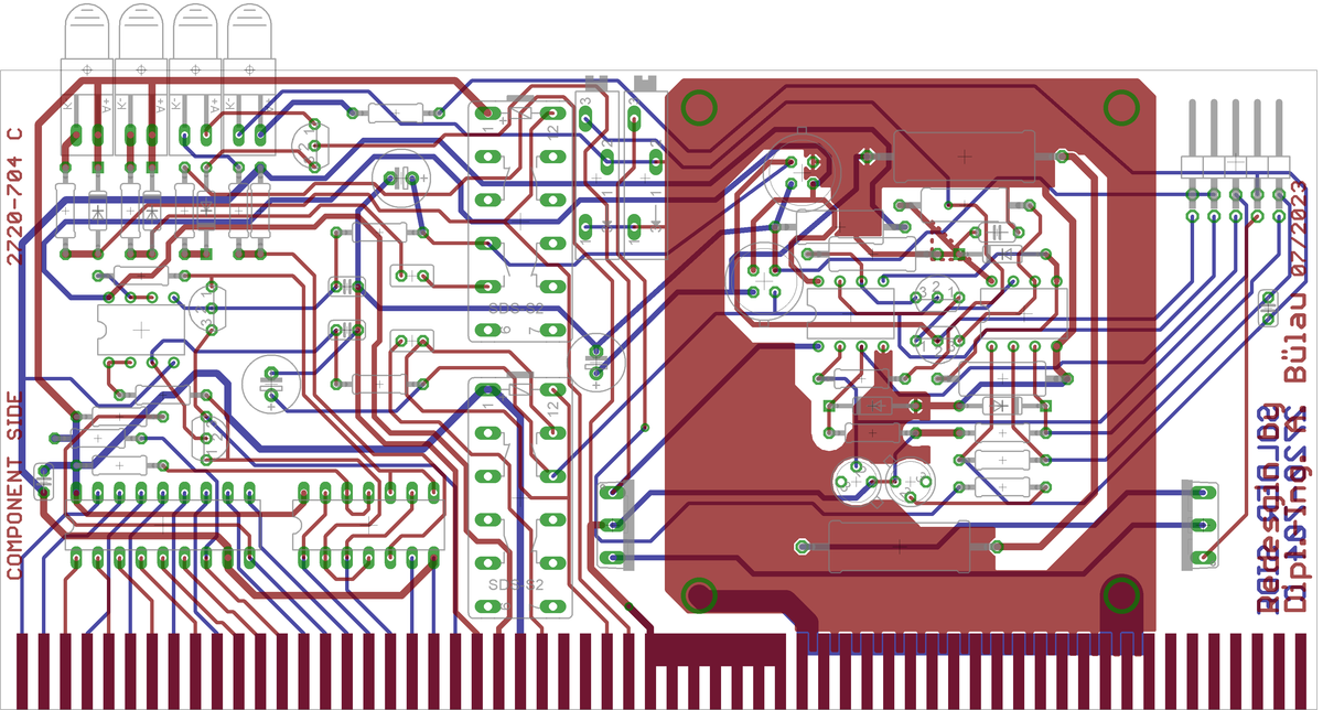
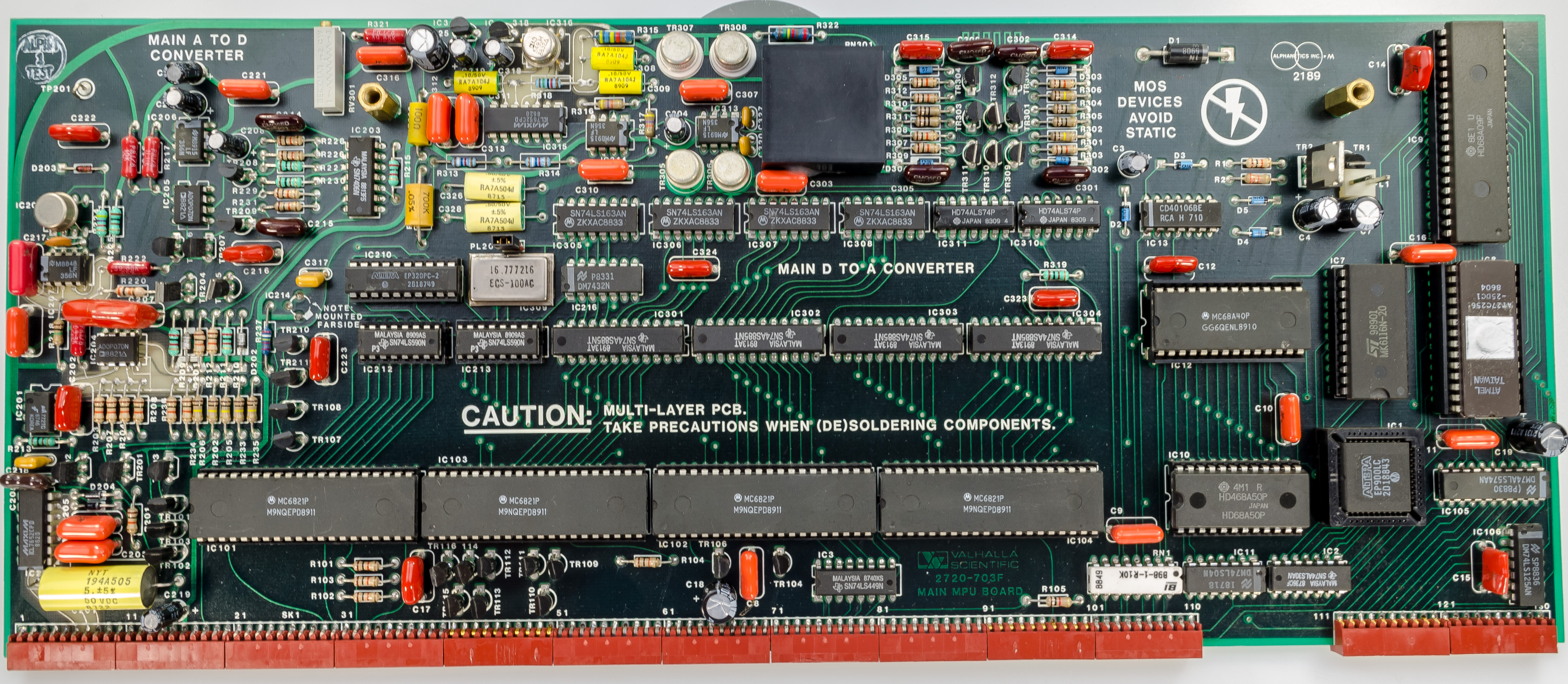
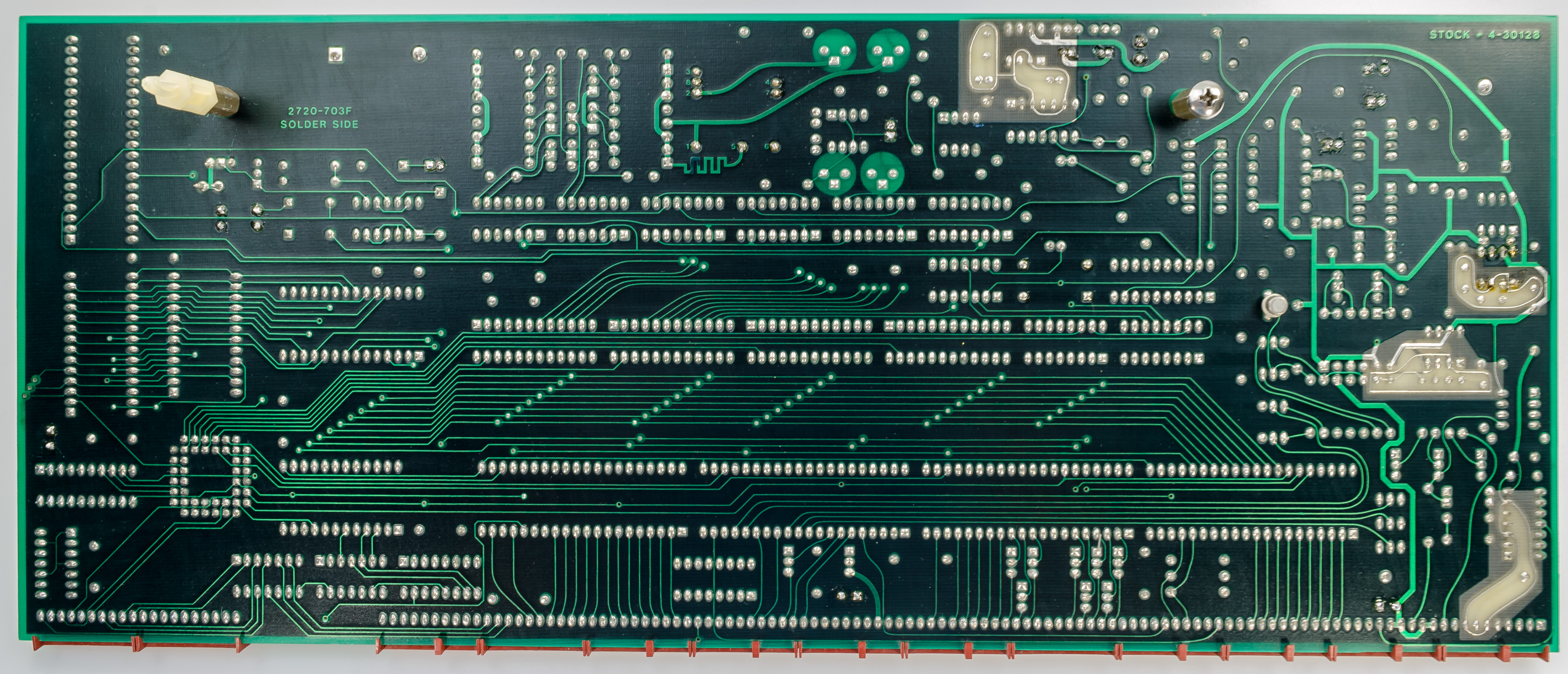
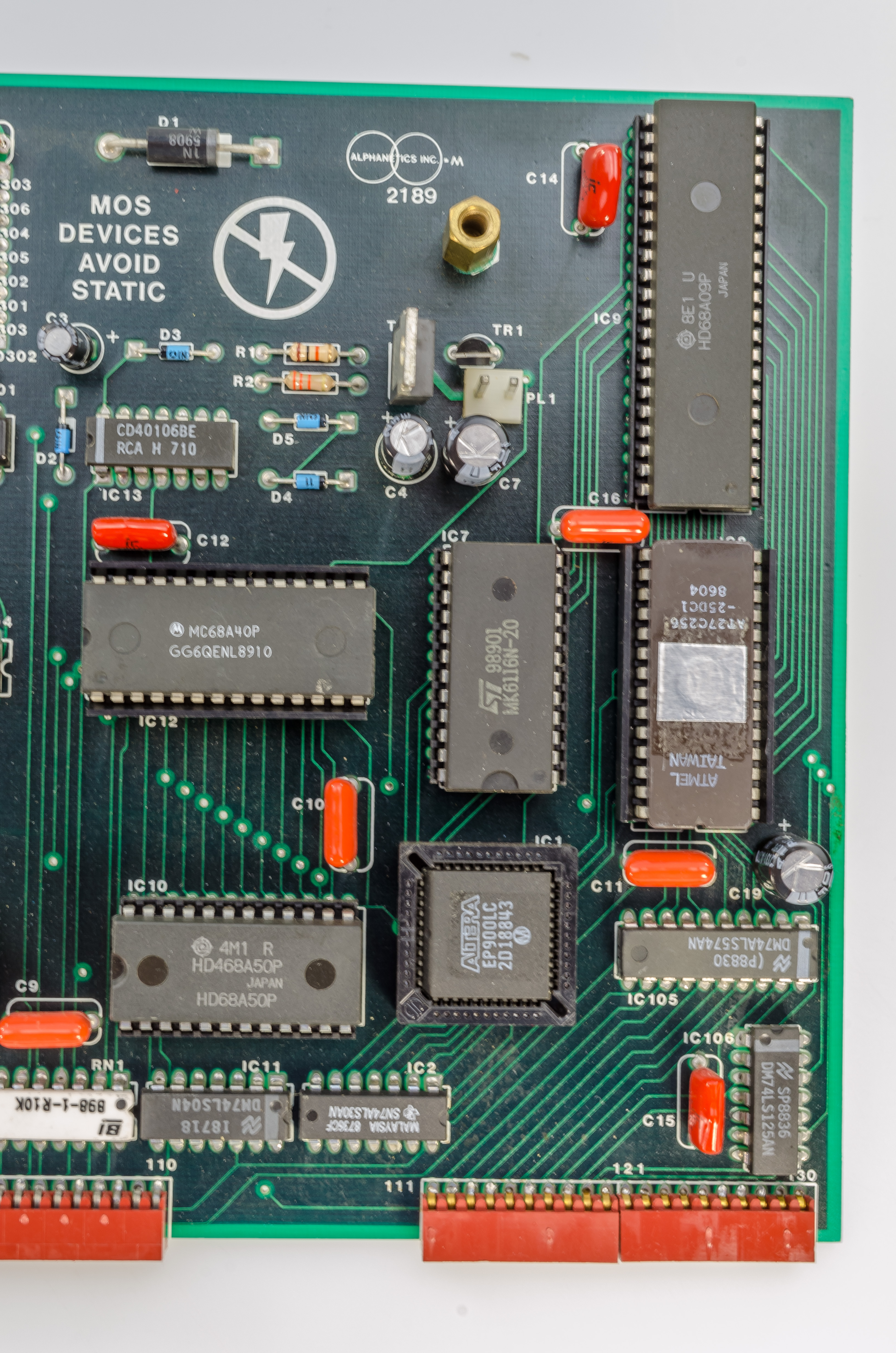
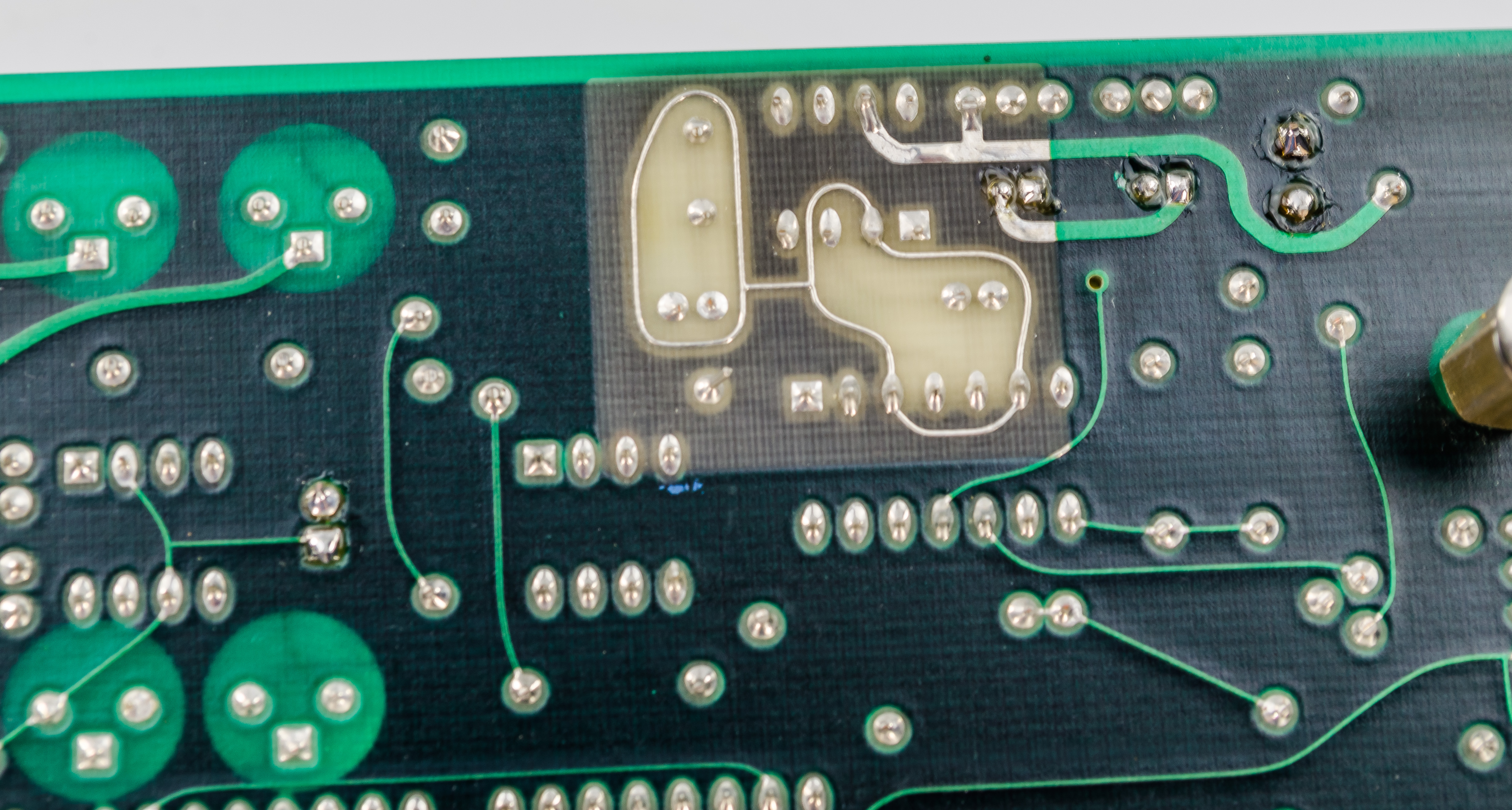
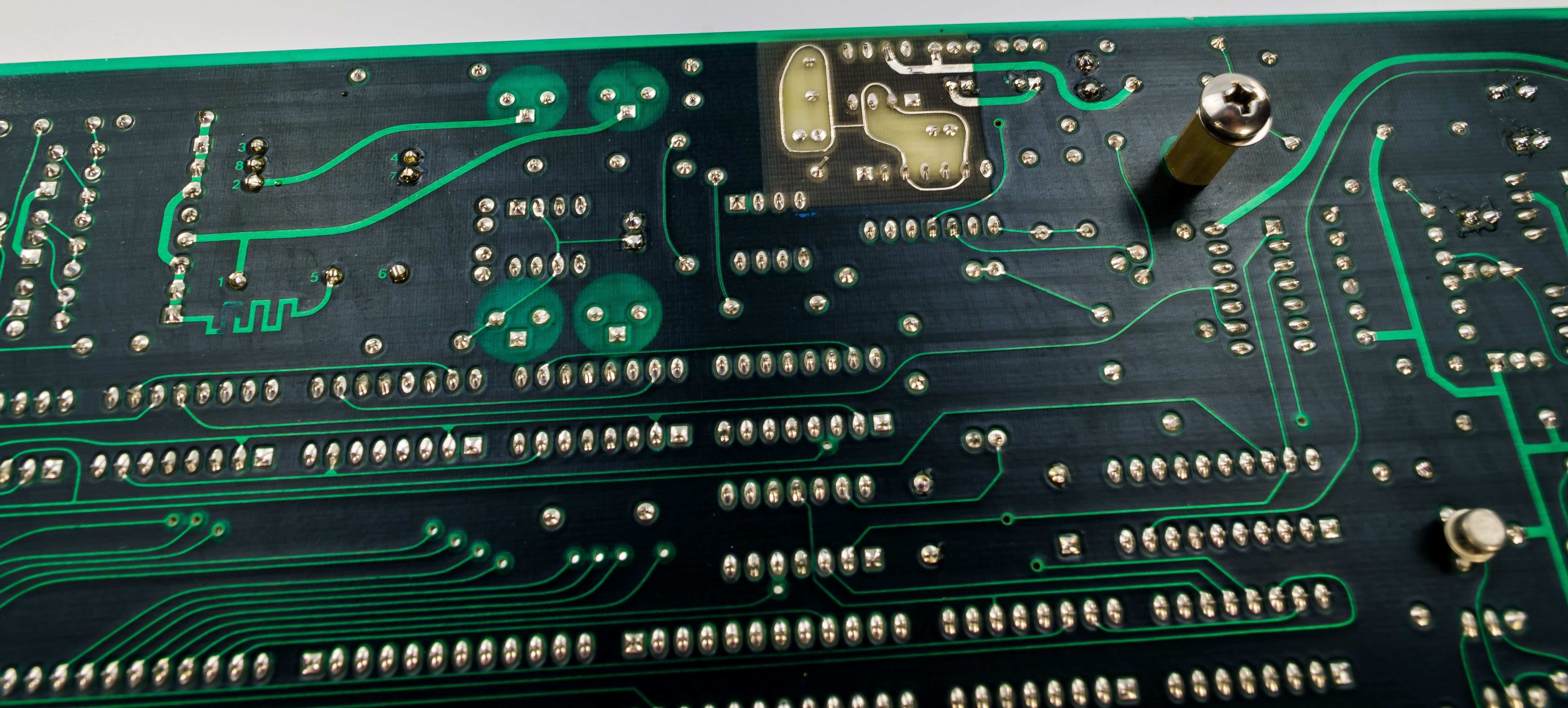
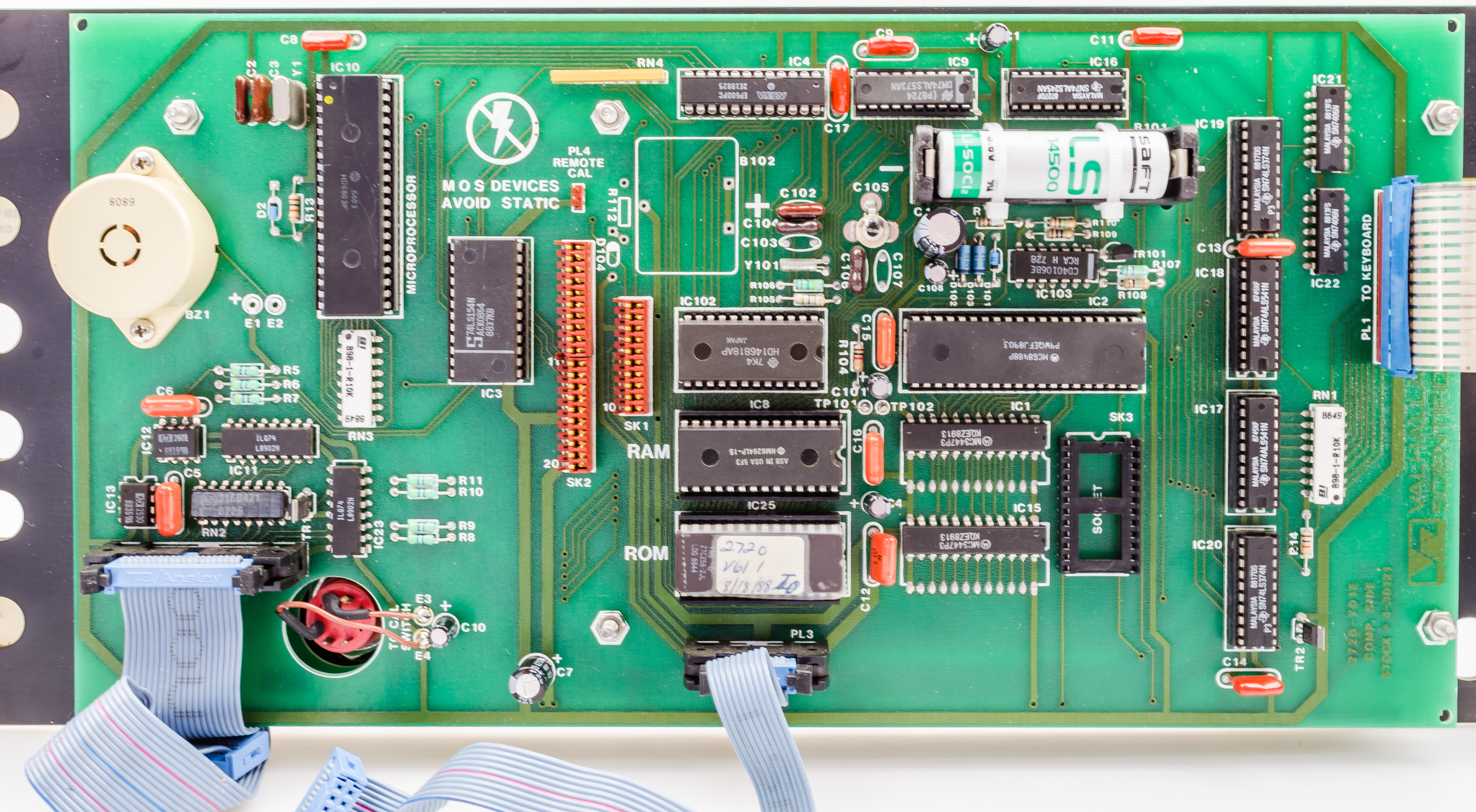
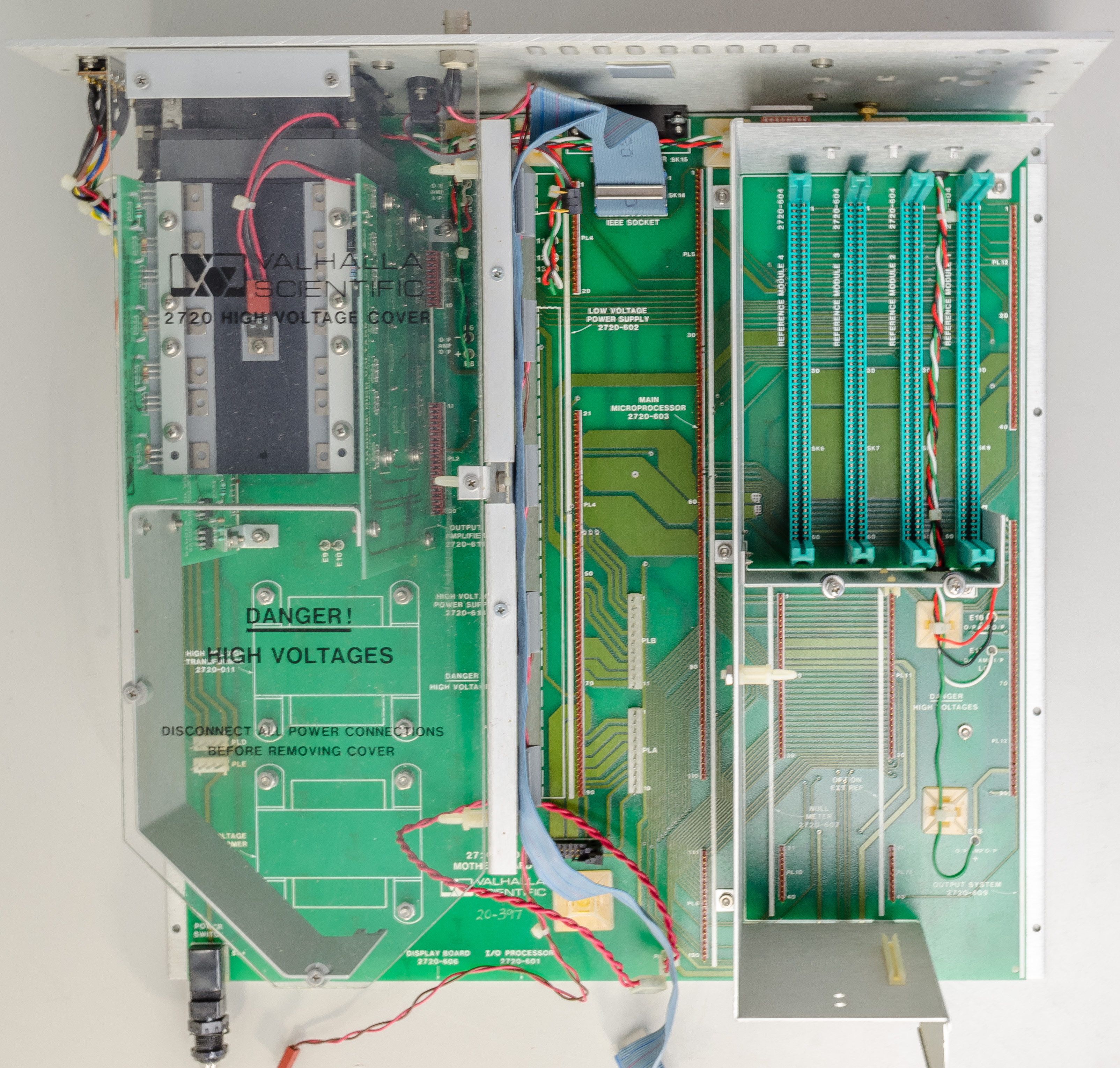
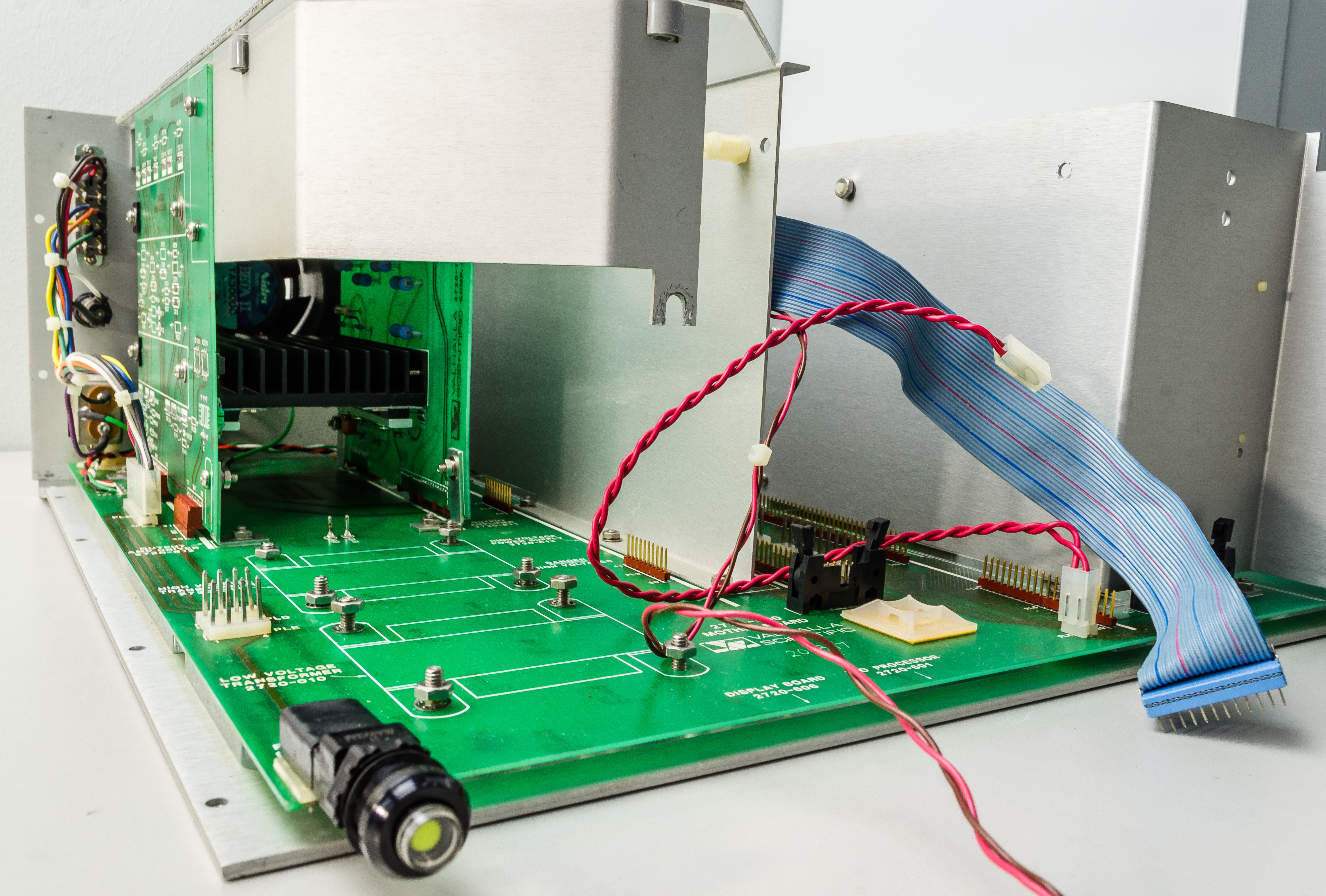
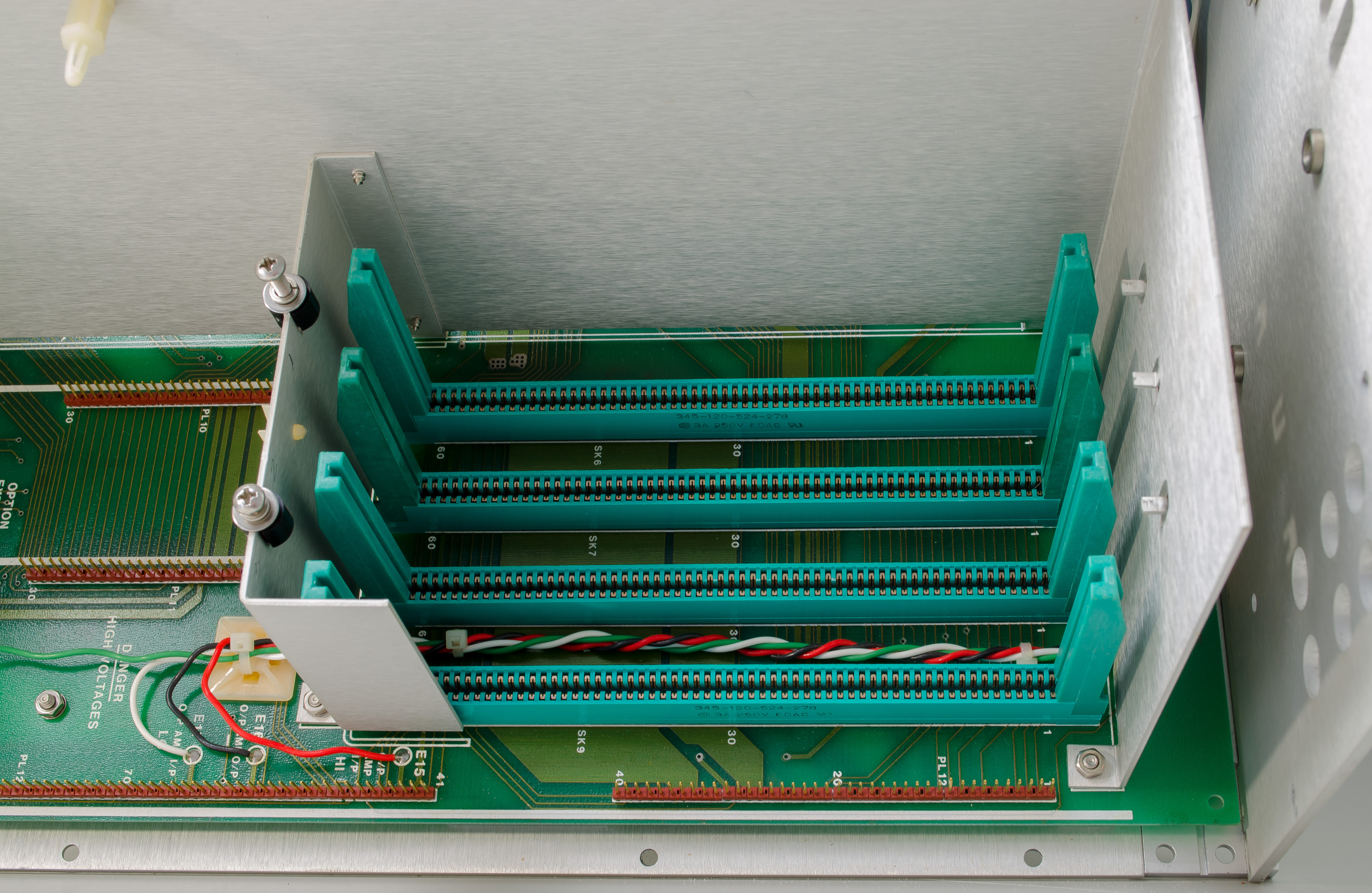
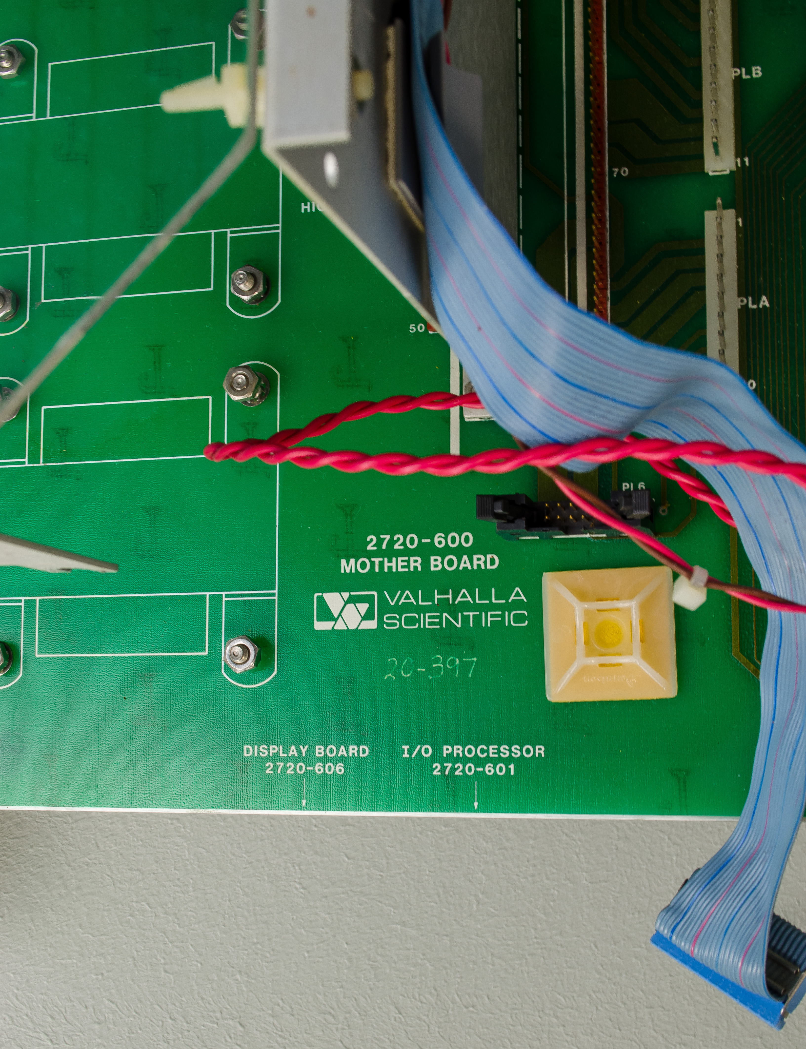
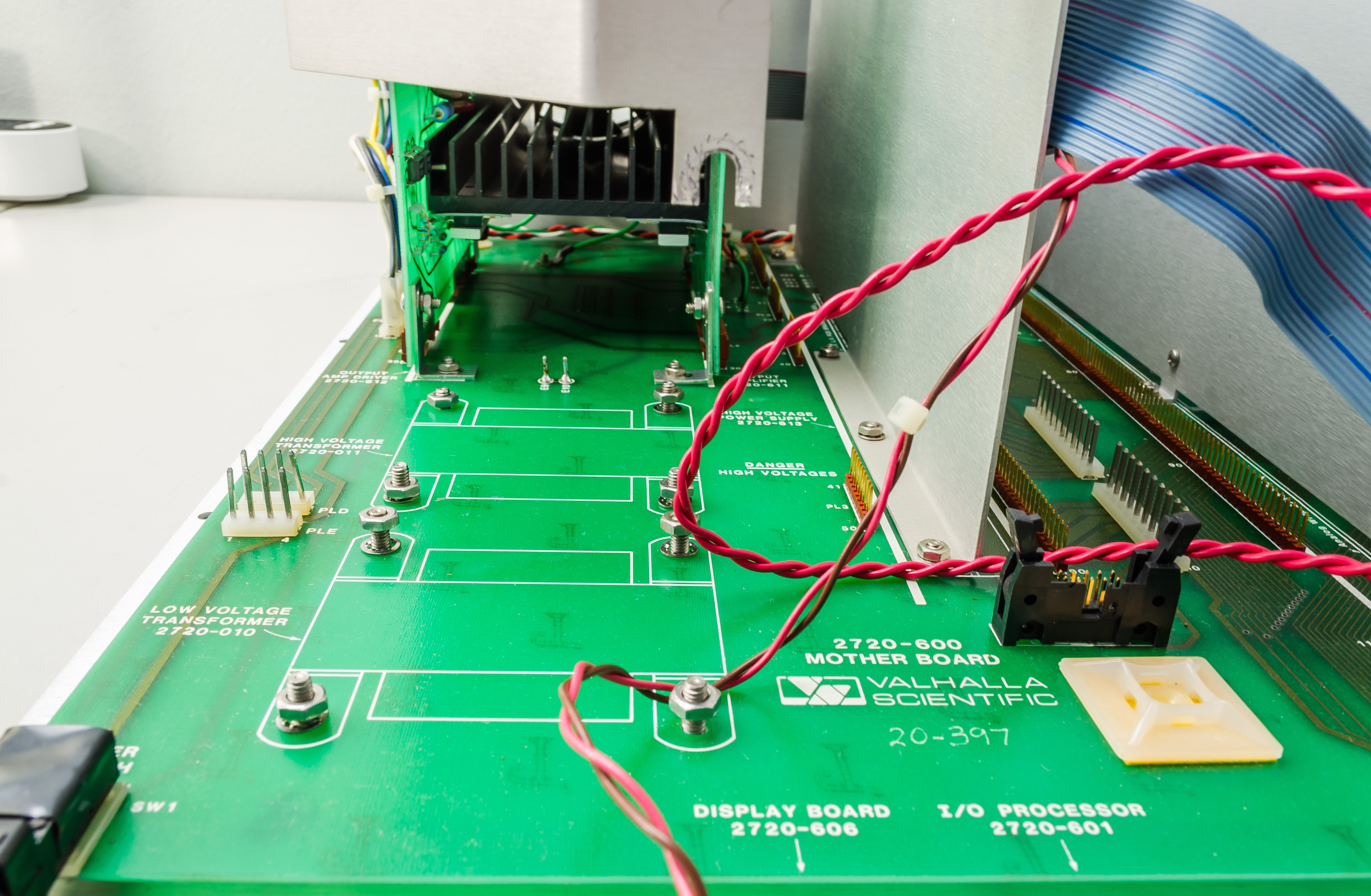
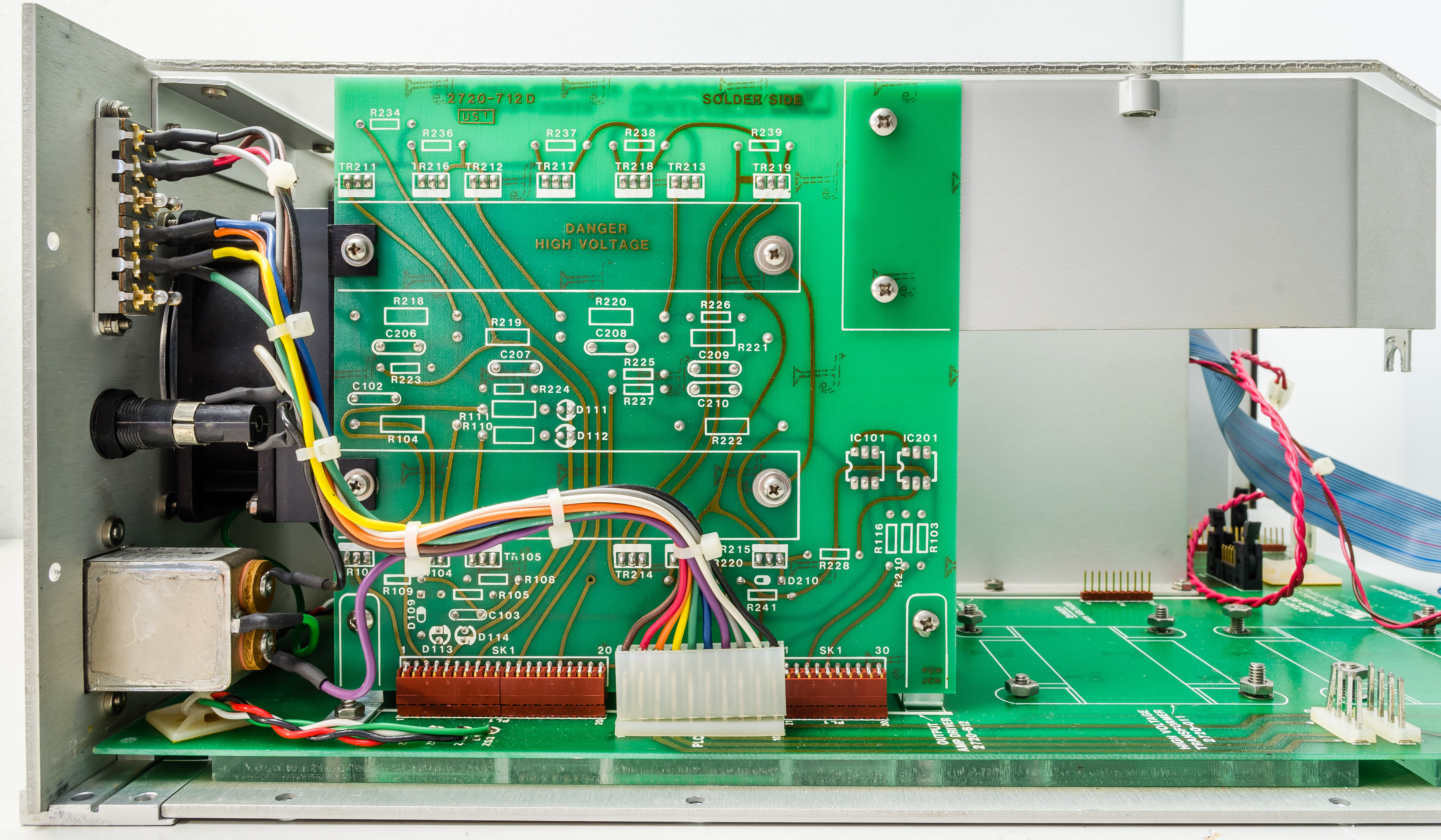
Tear-down and boards design
Let’s take a look of 2720GS insides.
Front panel
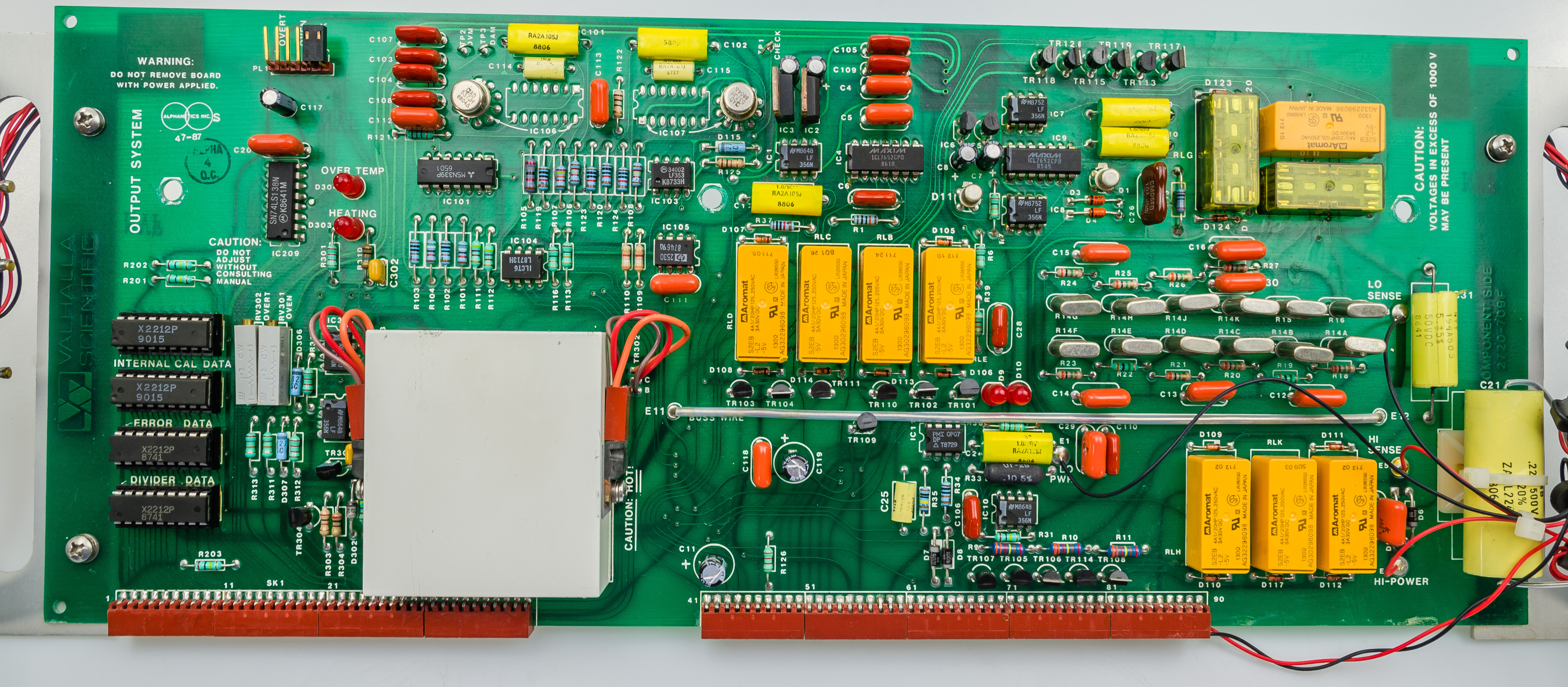
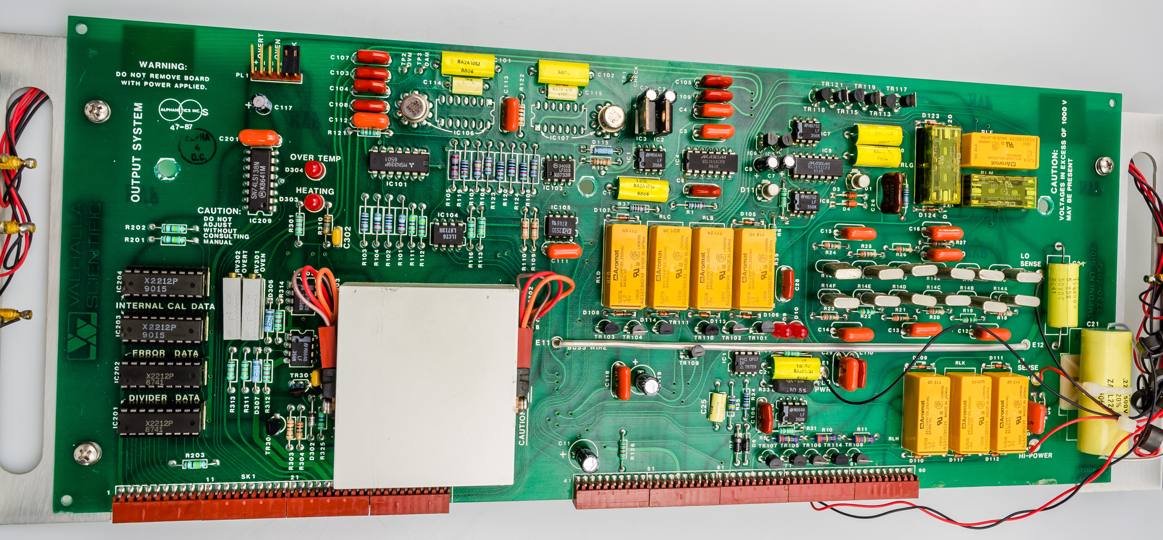
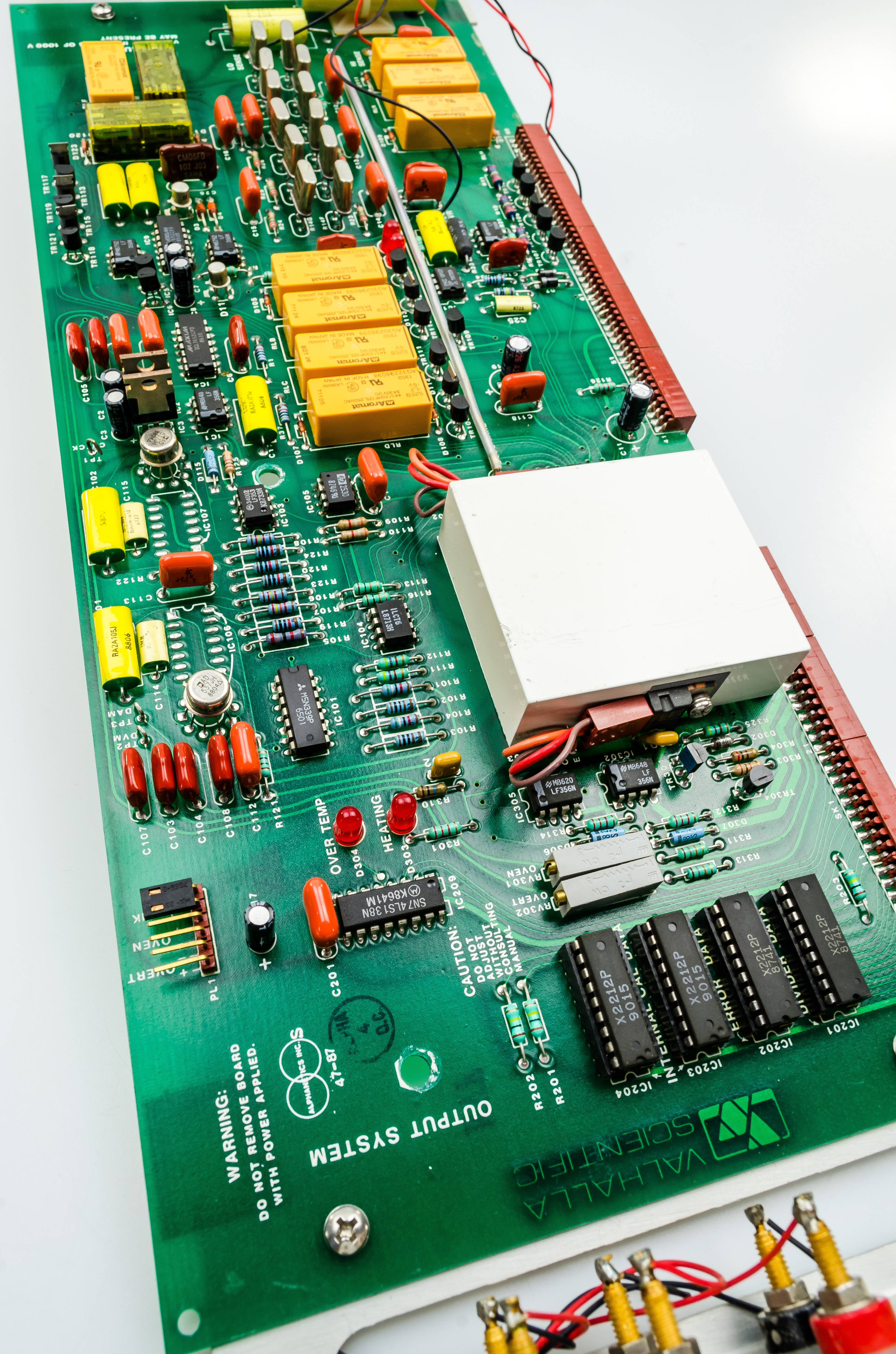
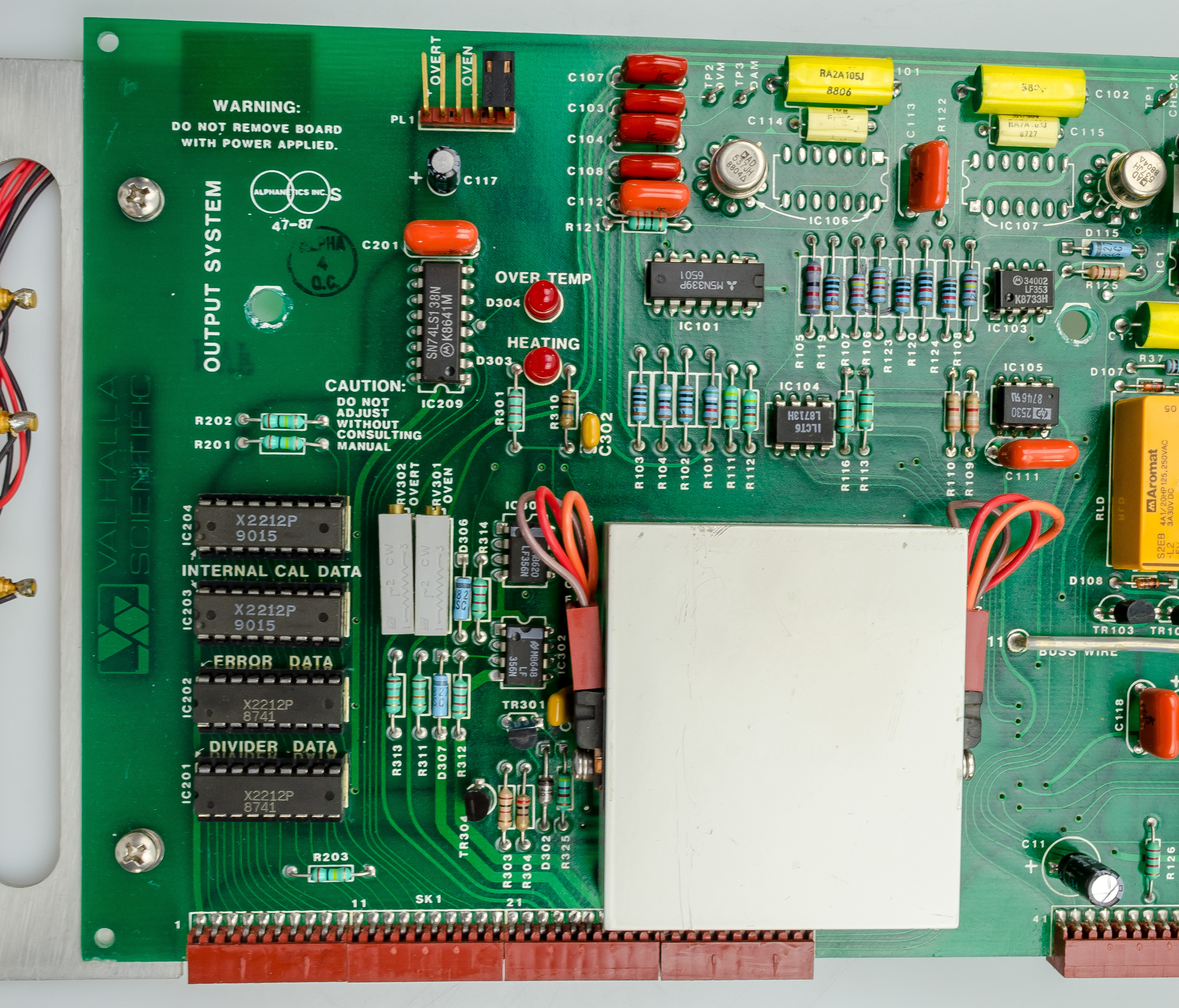
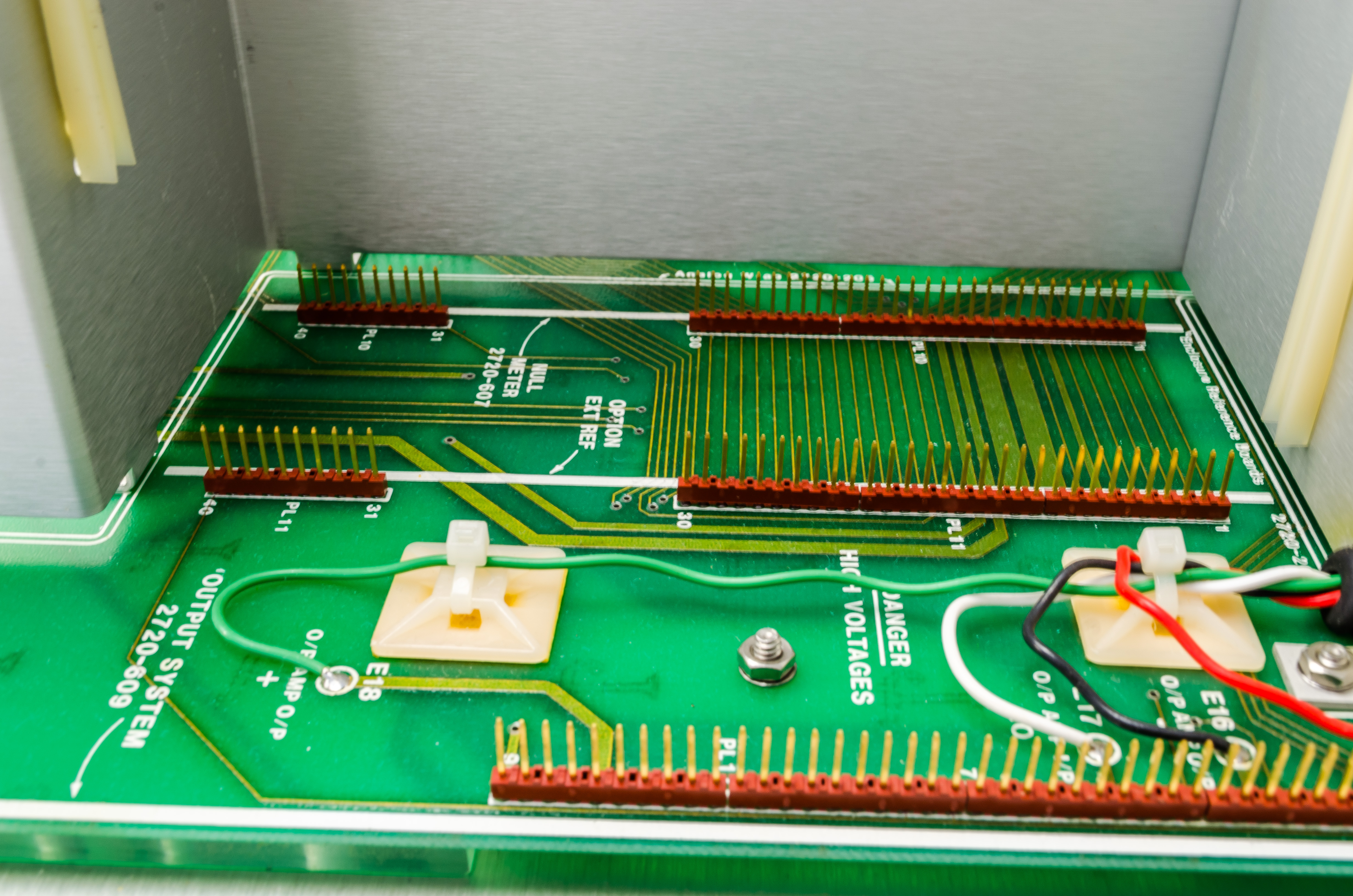
Output system PCBA
Output amplifier PCBA
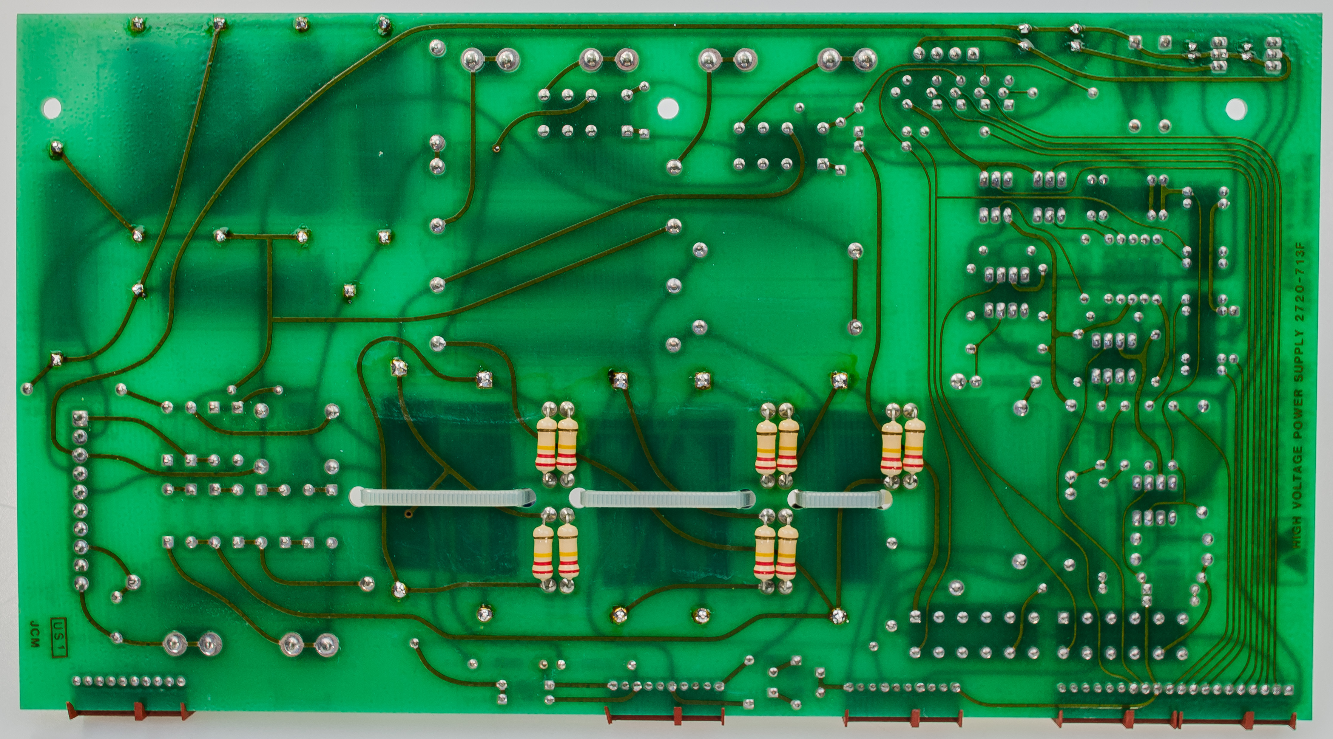
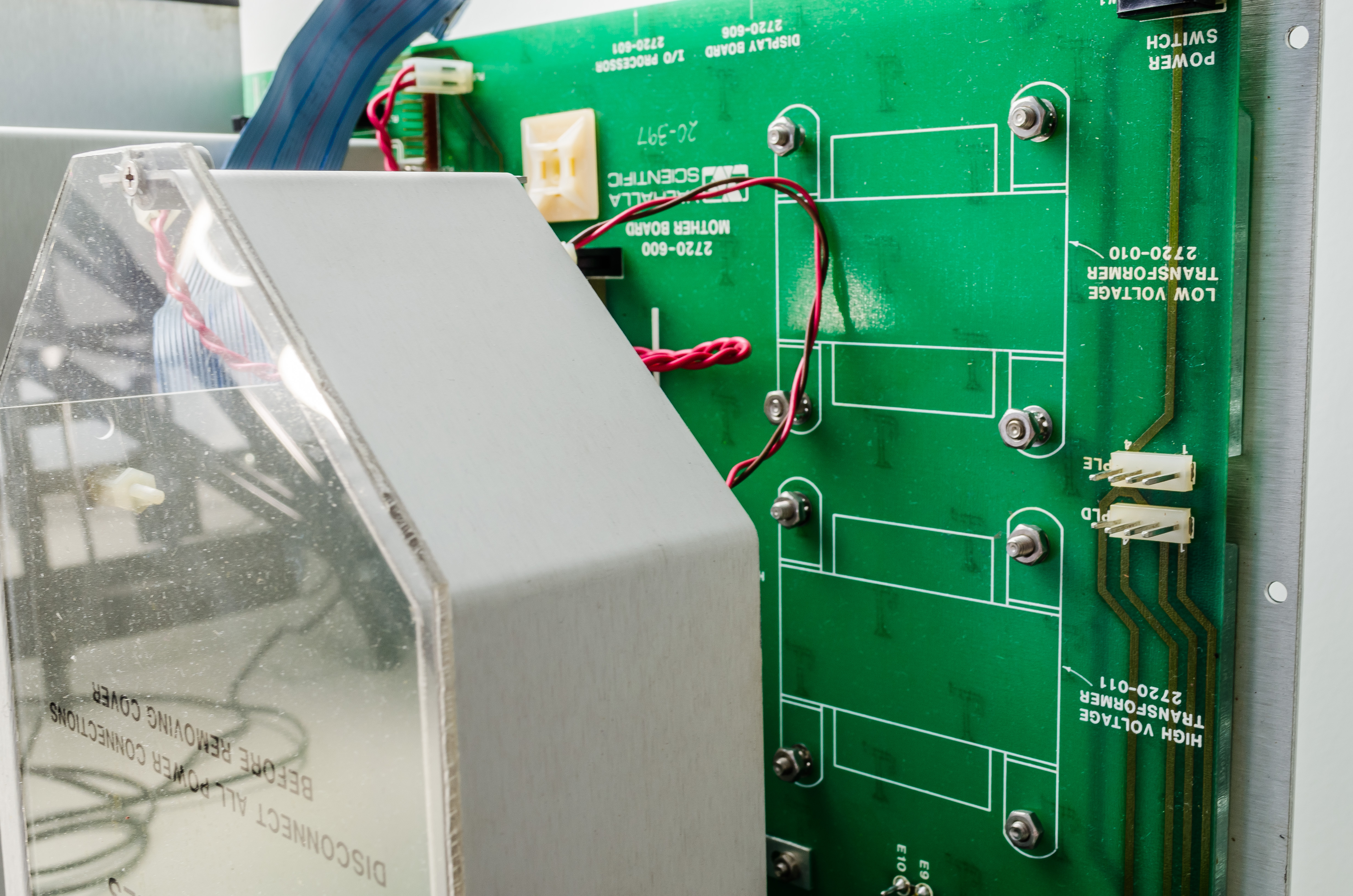
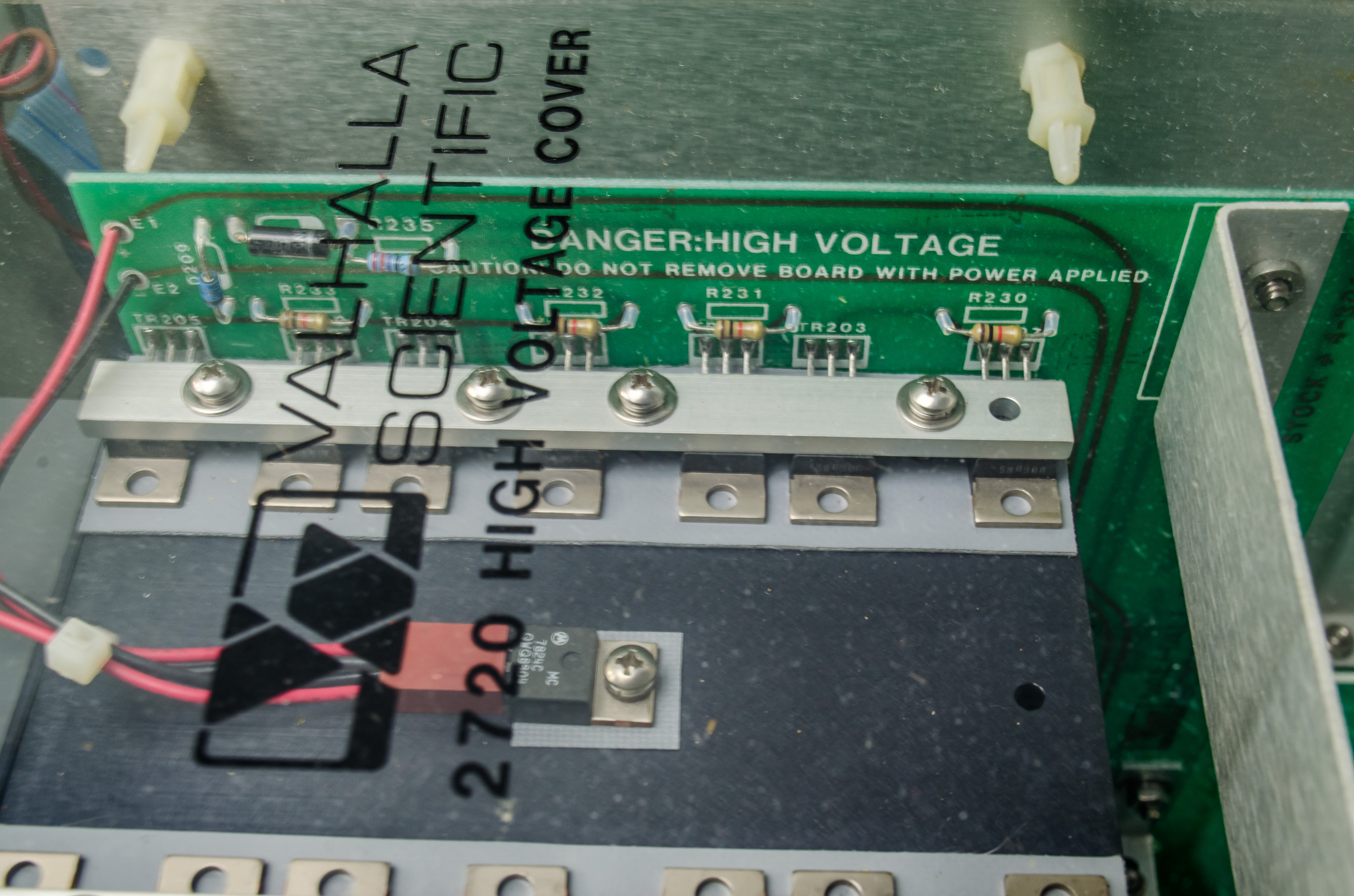
High voltage power supply
Low voltage power supply
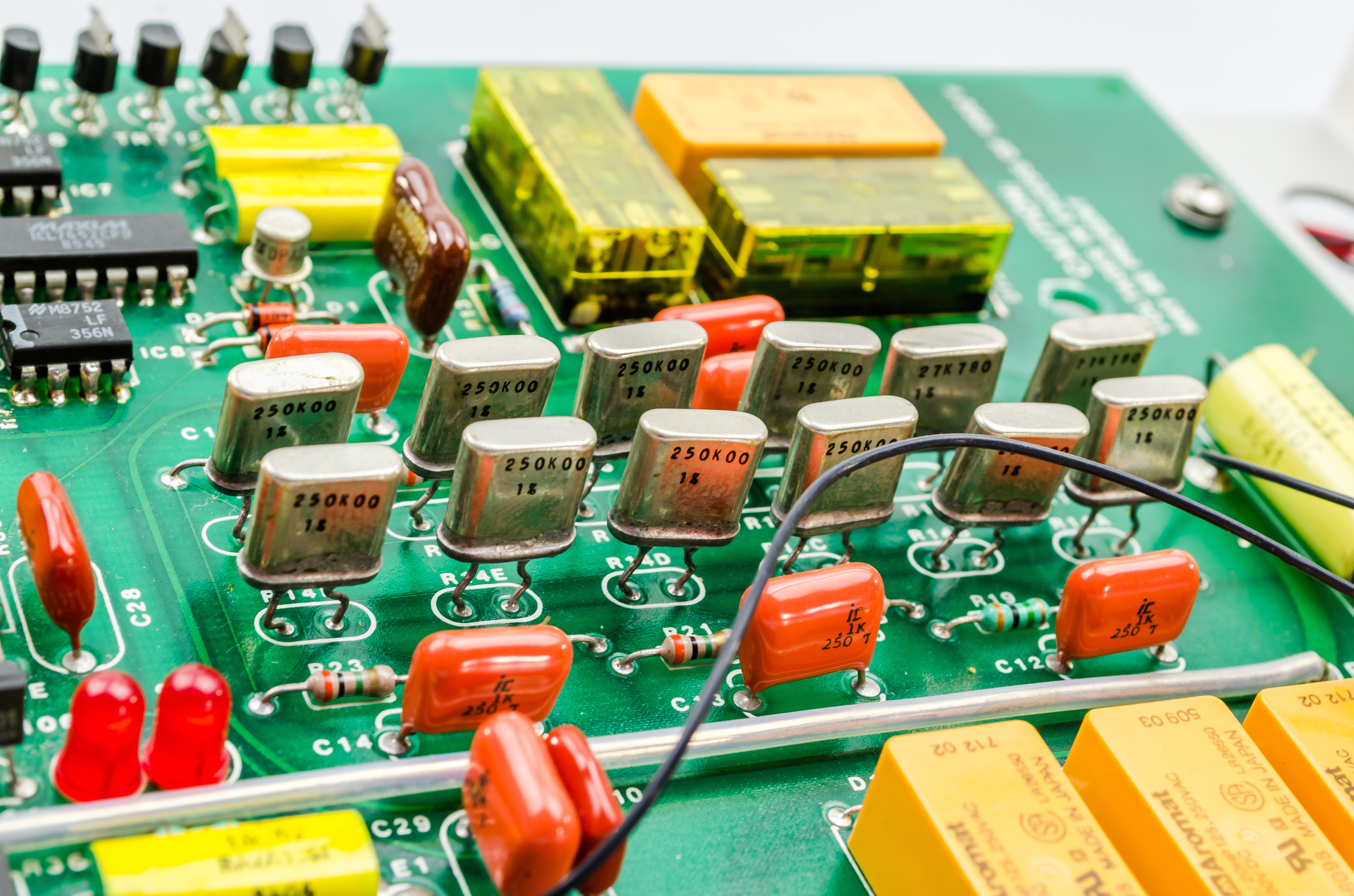
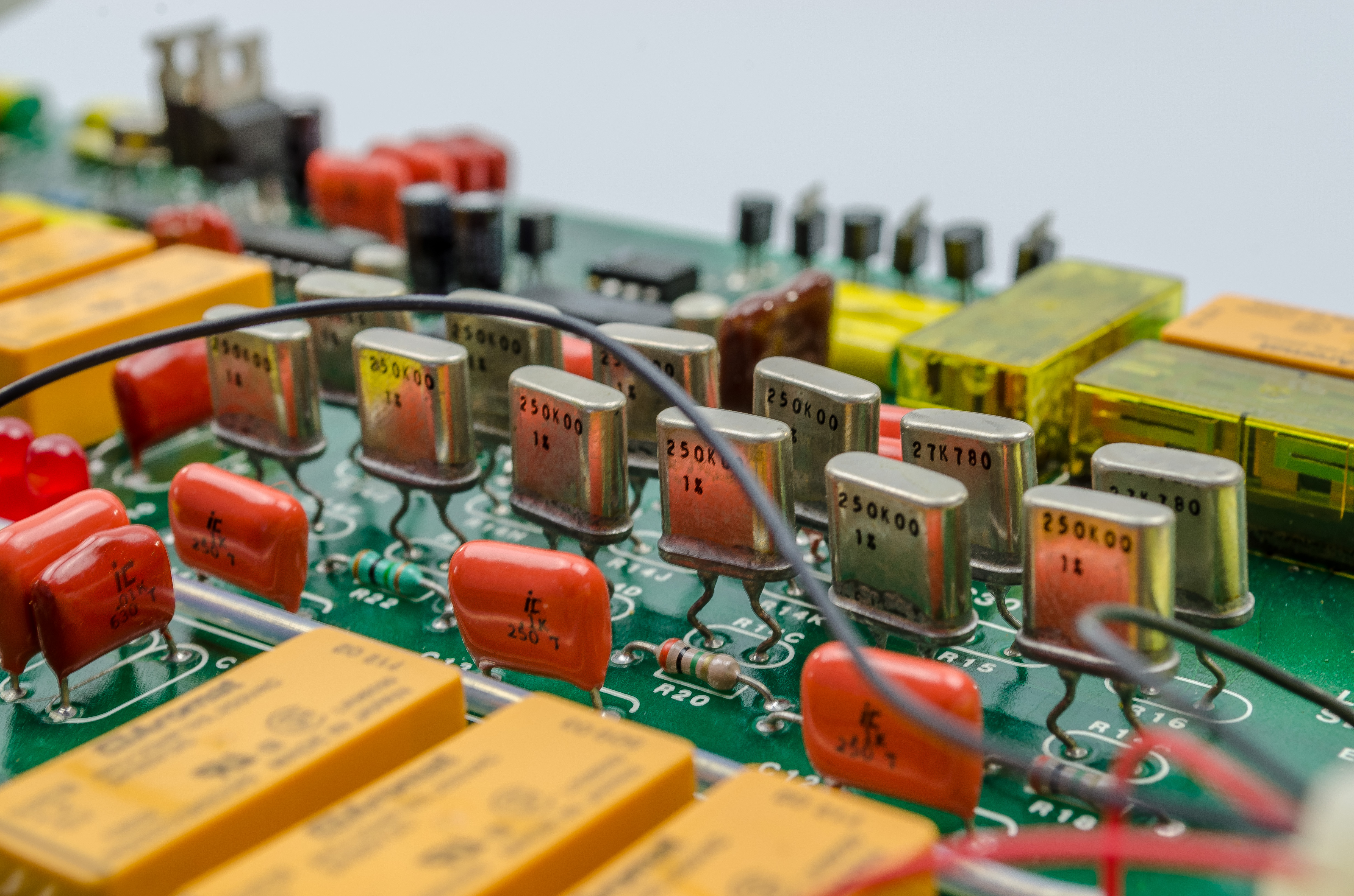
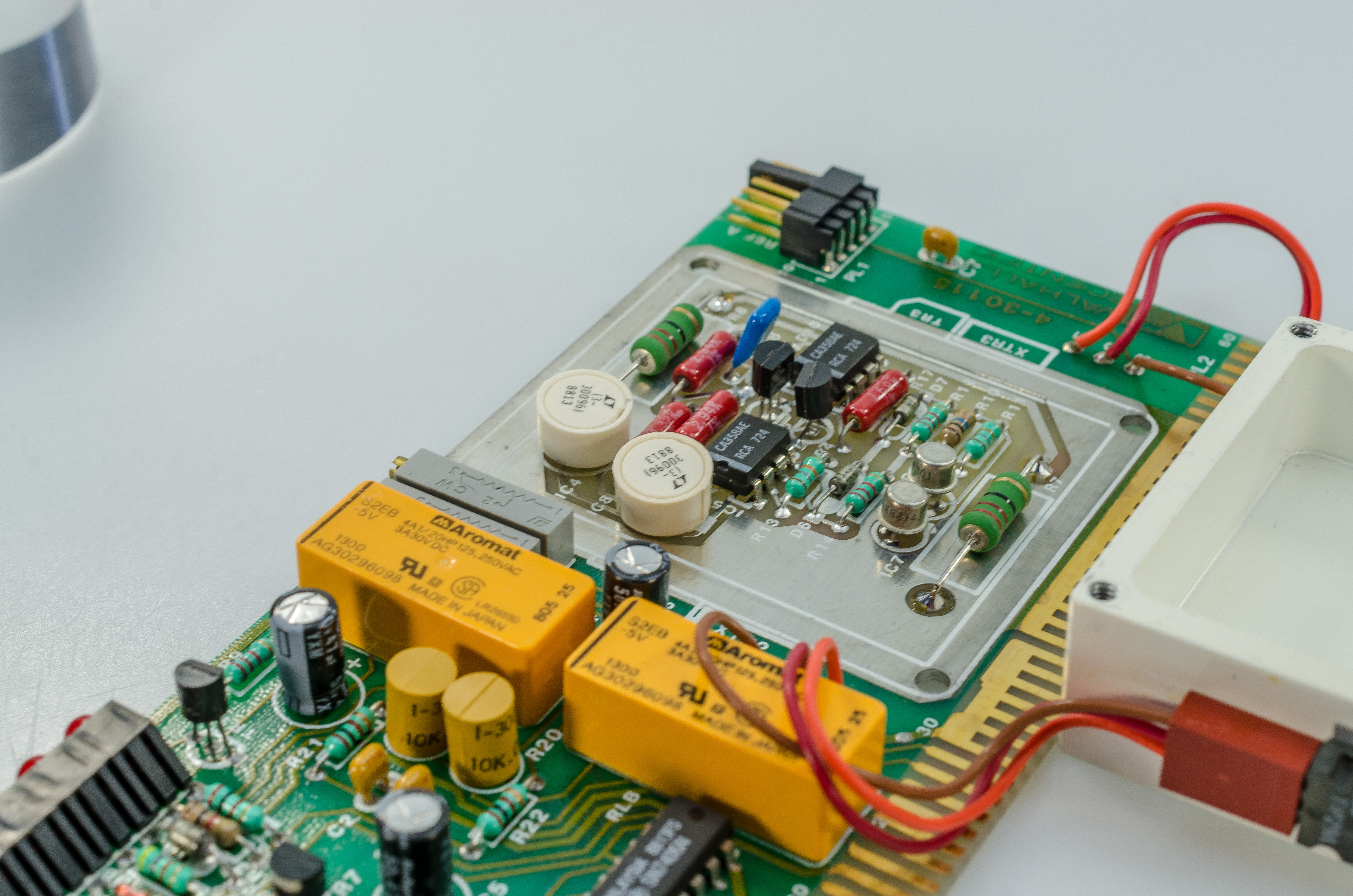
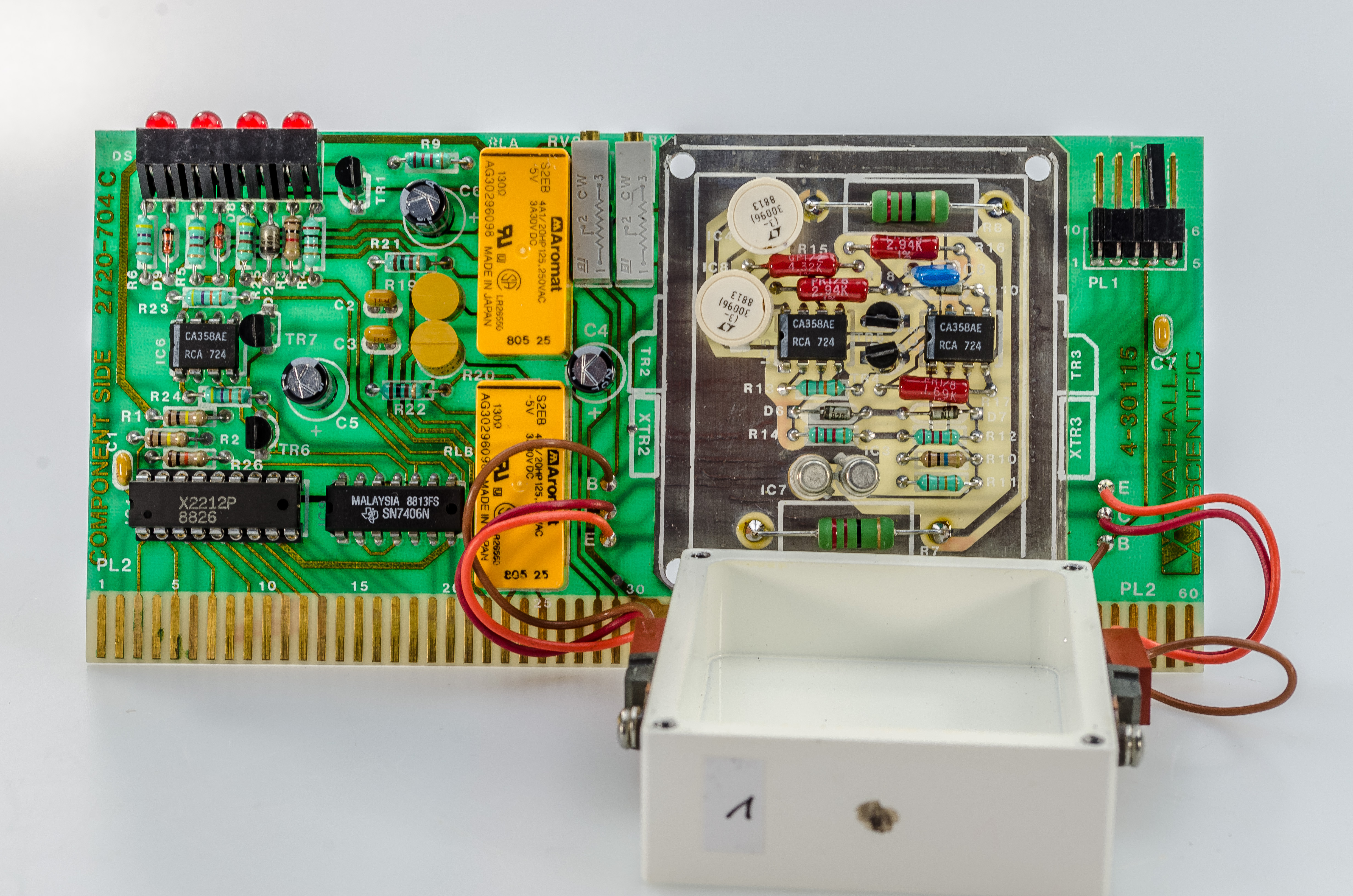
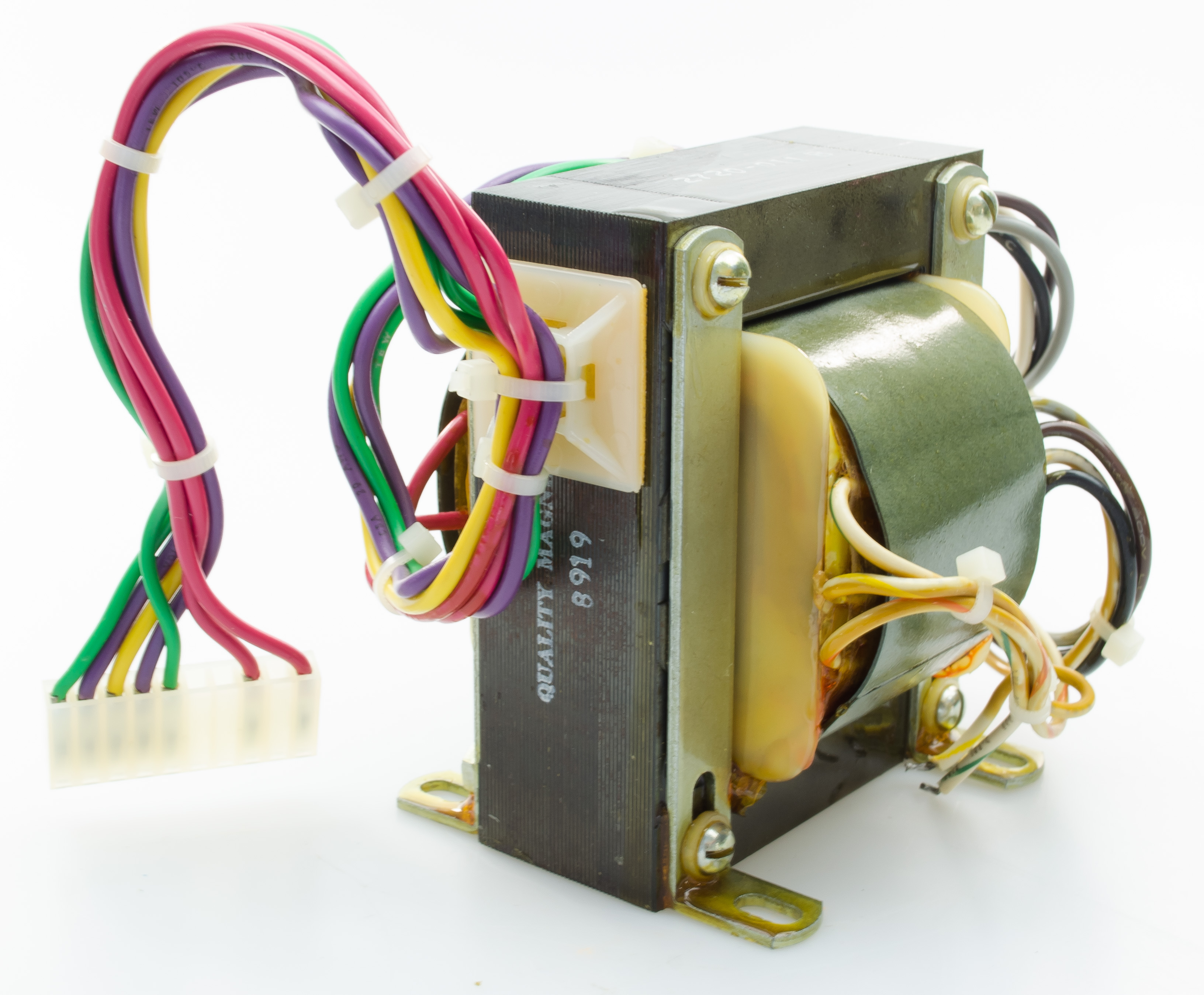
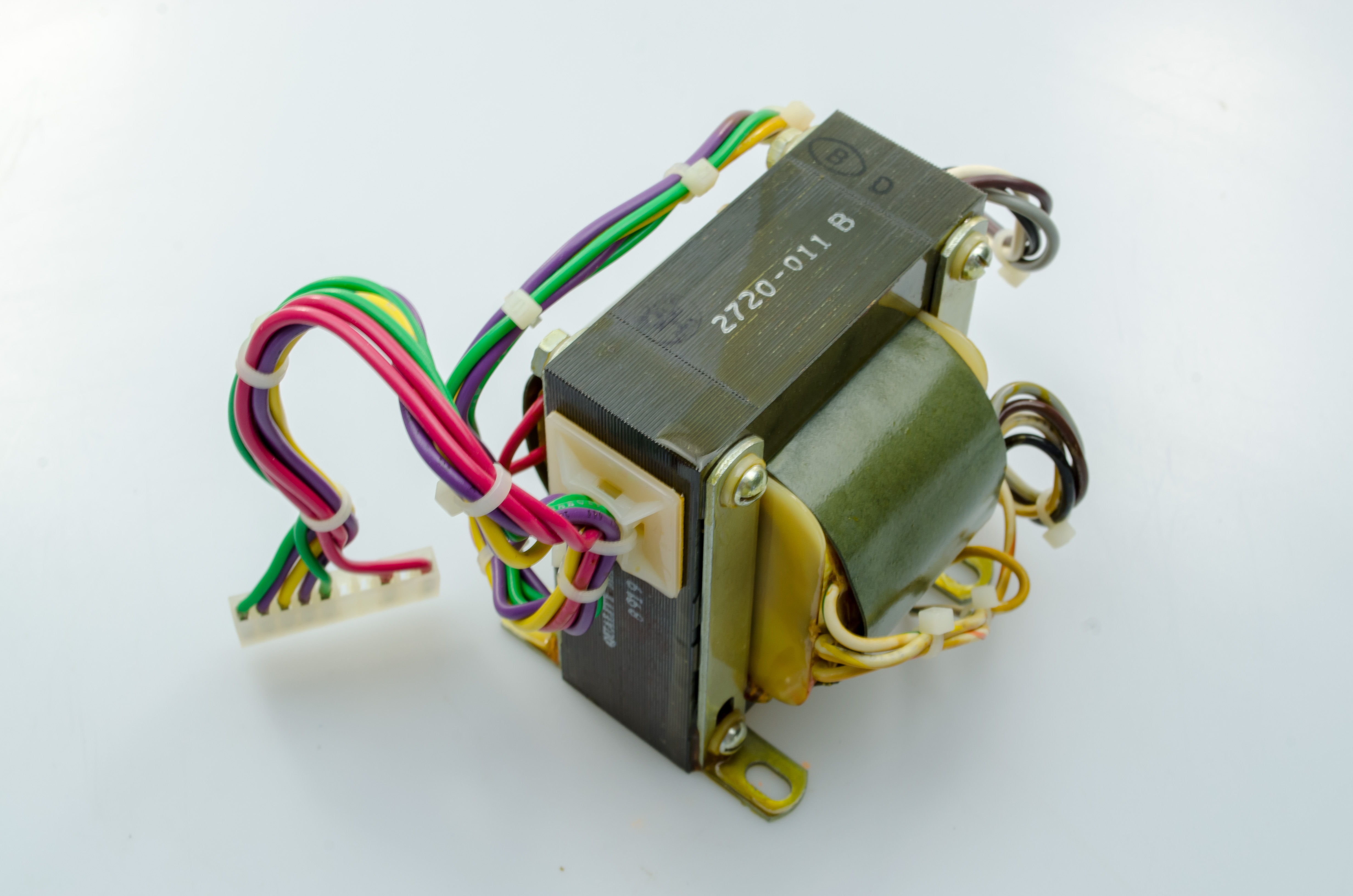
Reference module
This particular 2720GS is equipped with three reference modules, each having two LM399 ovenized zener references.
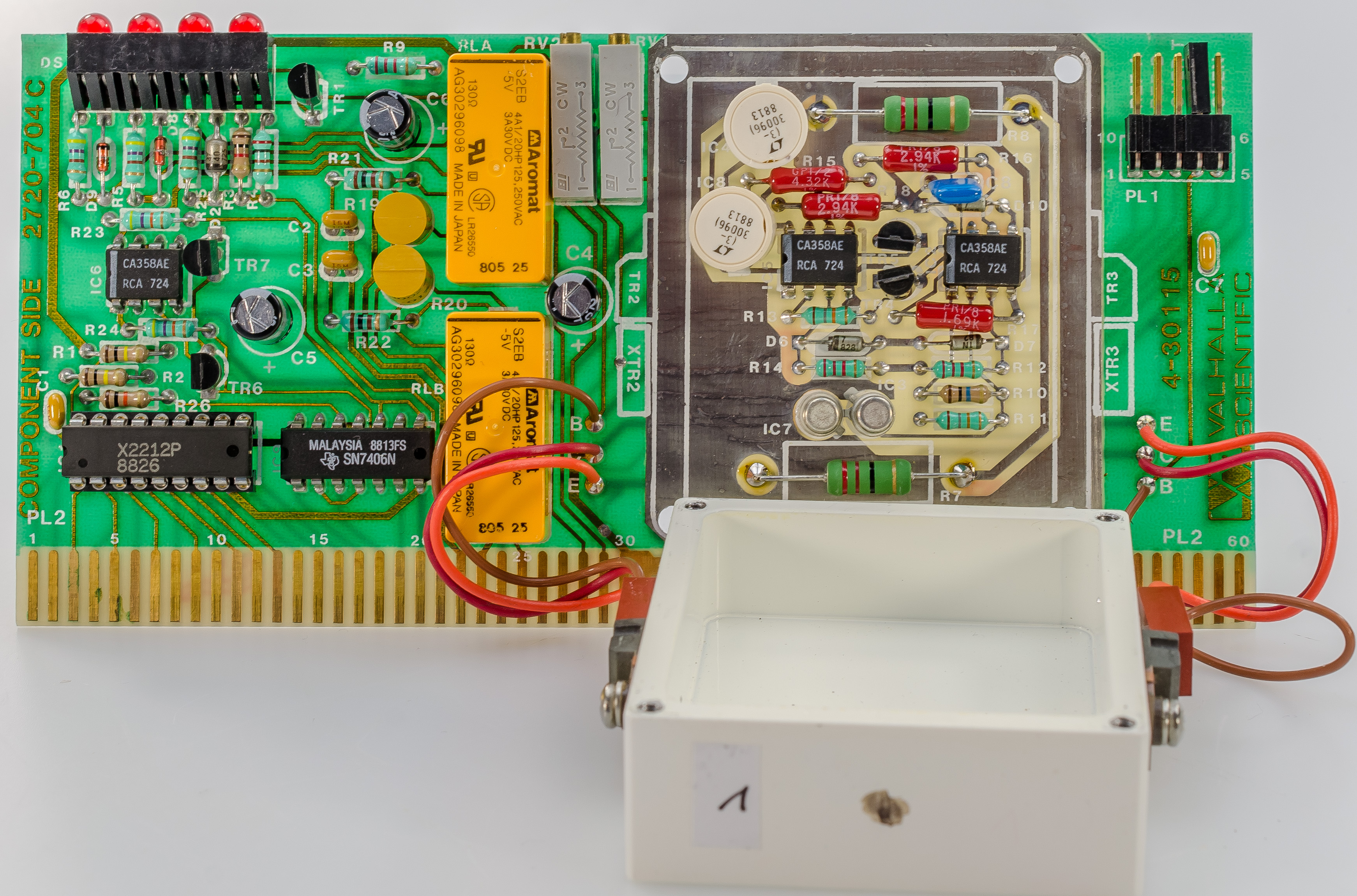
As a future project, I’ve also started designing replica with newer lower noise ADR1399 reference module:
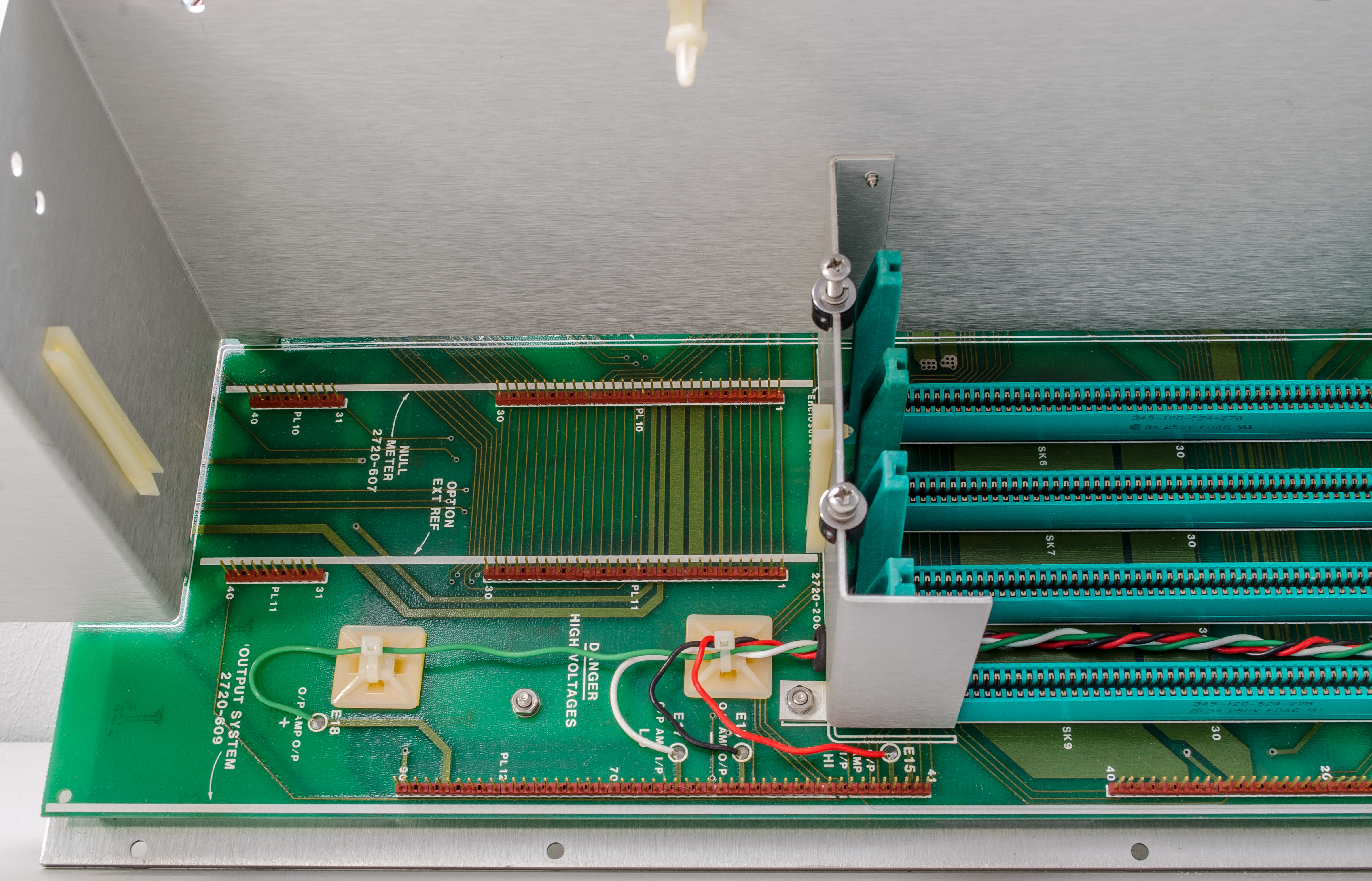
D/A and A/D assembly
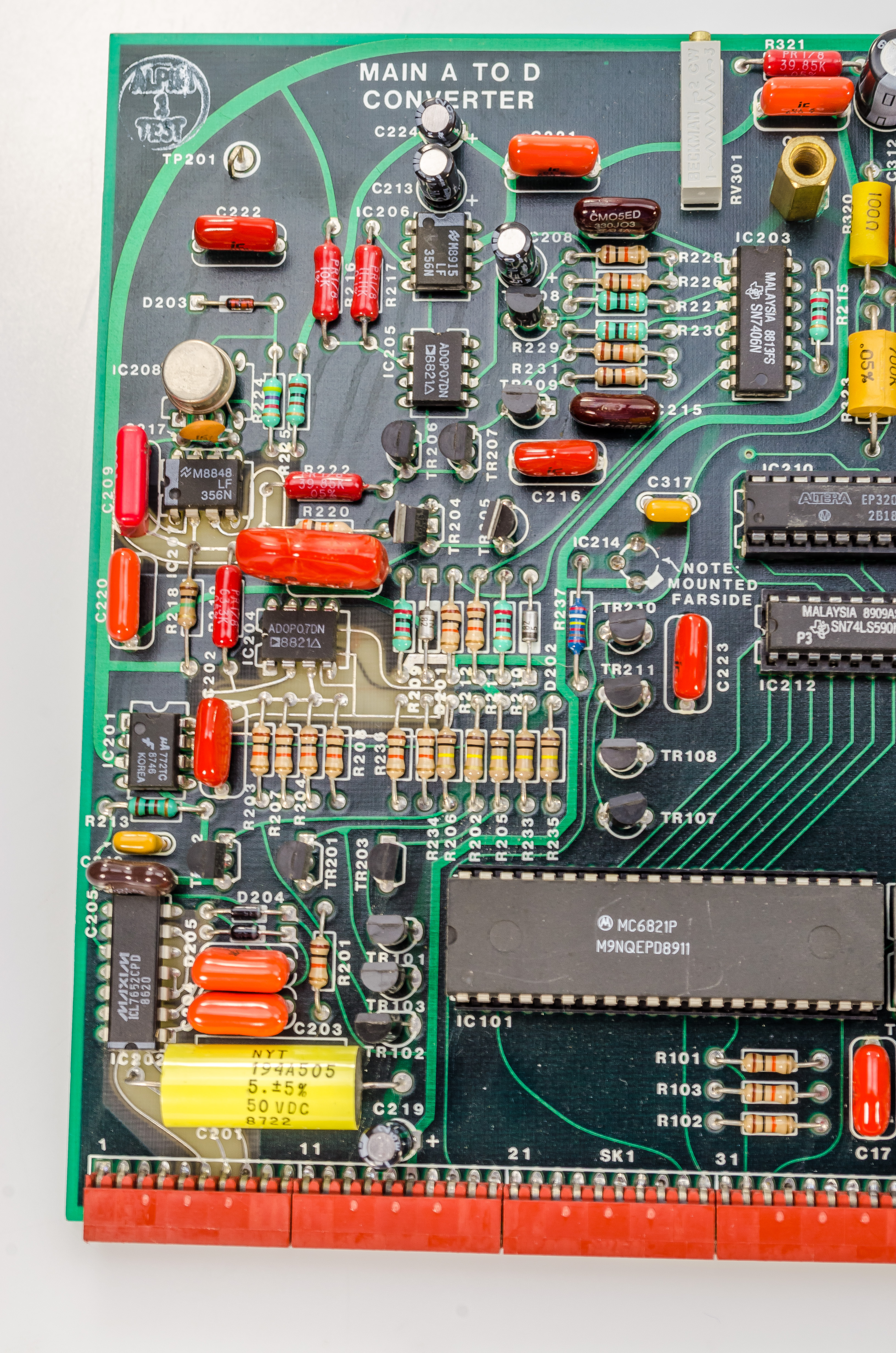
I/O Processor
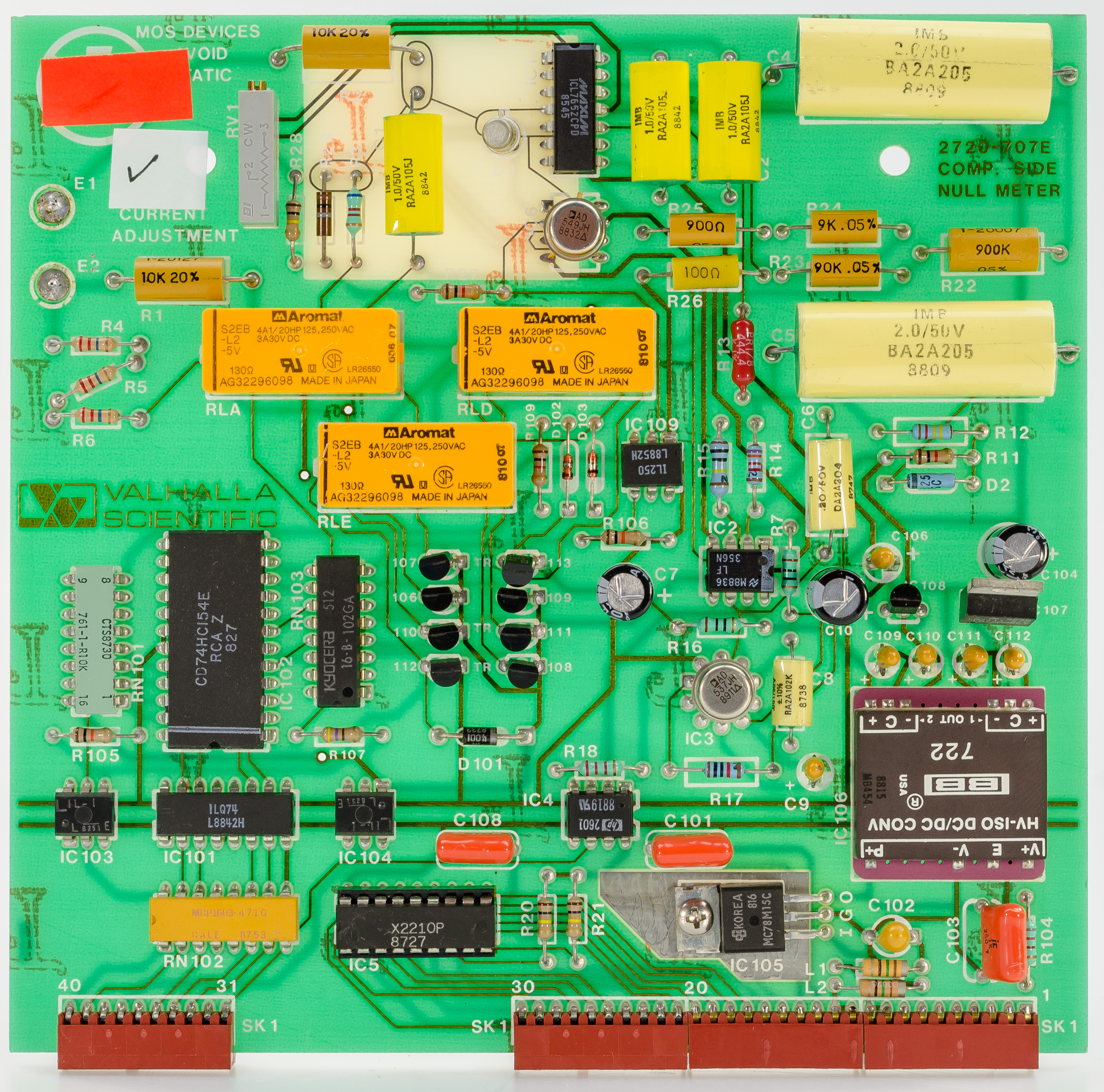
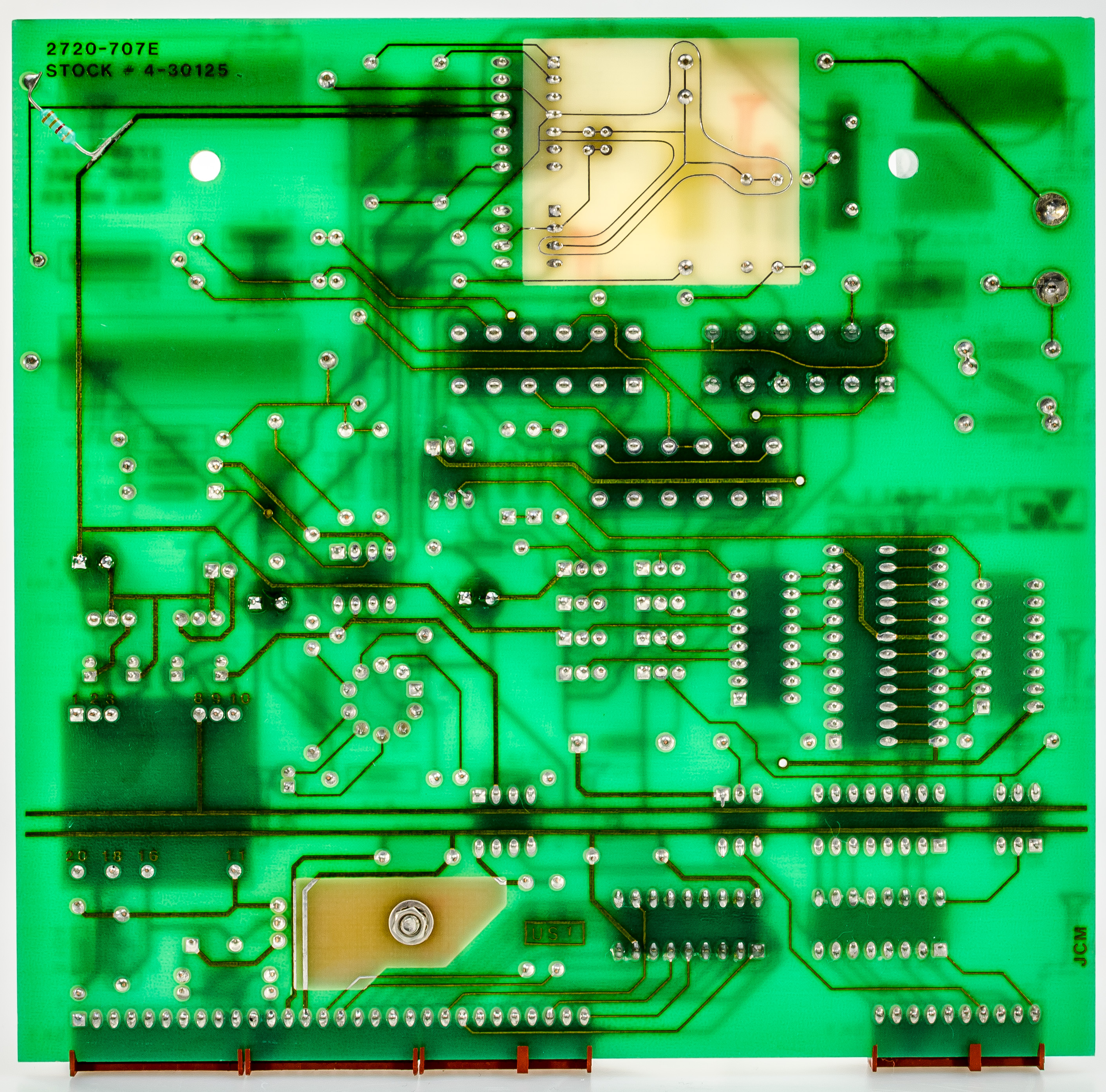
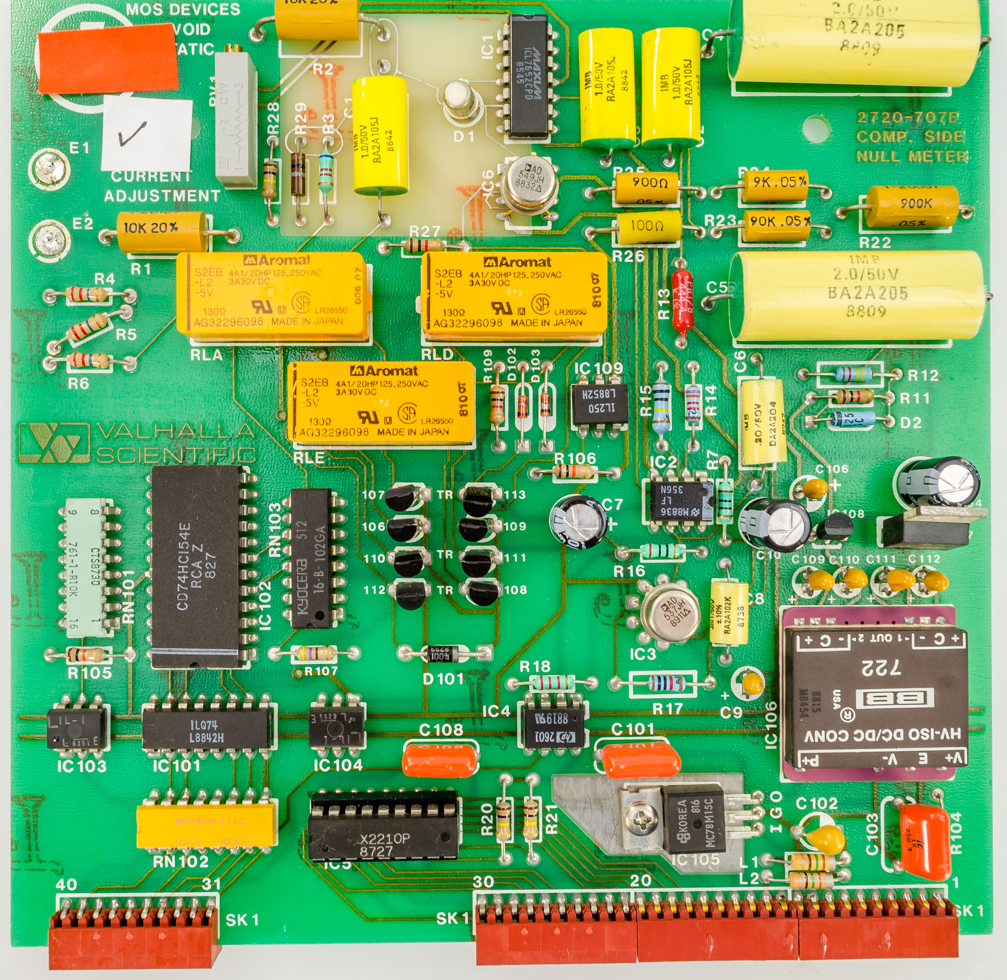
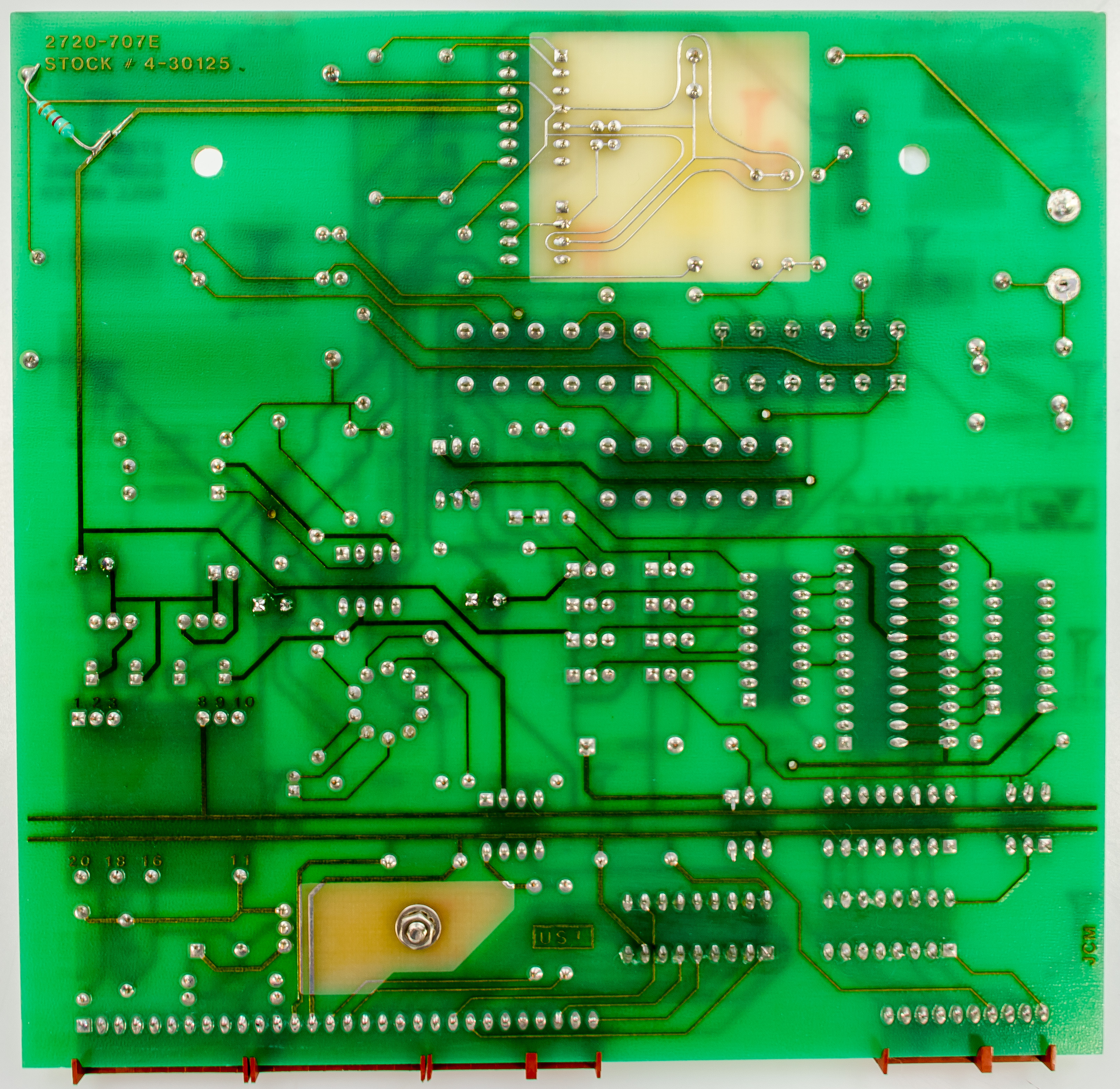
Null-meter assembly
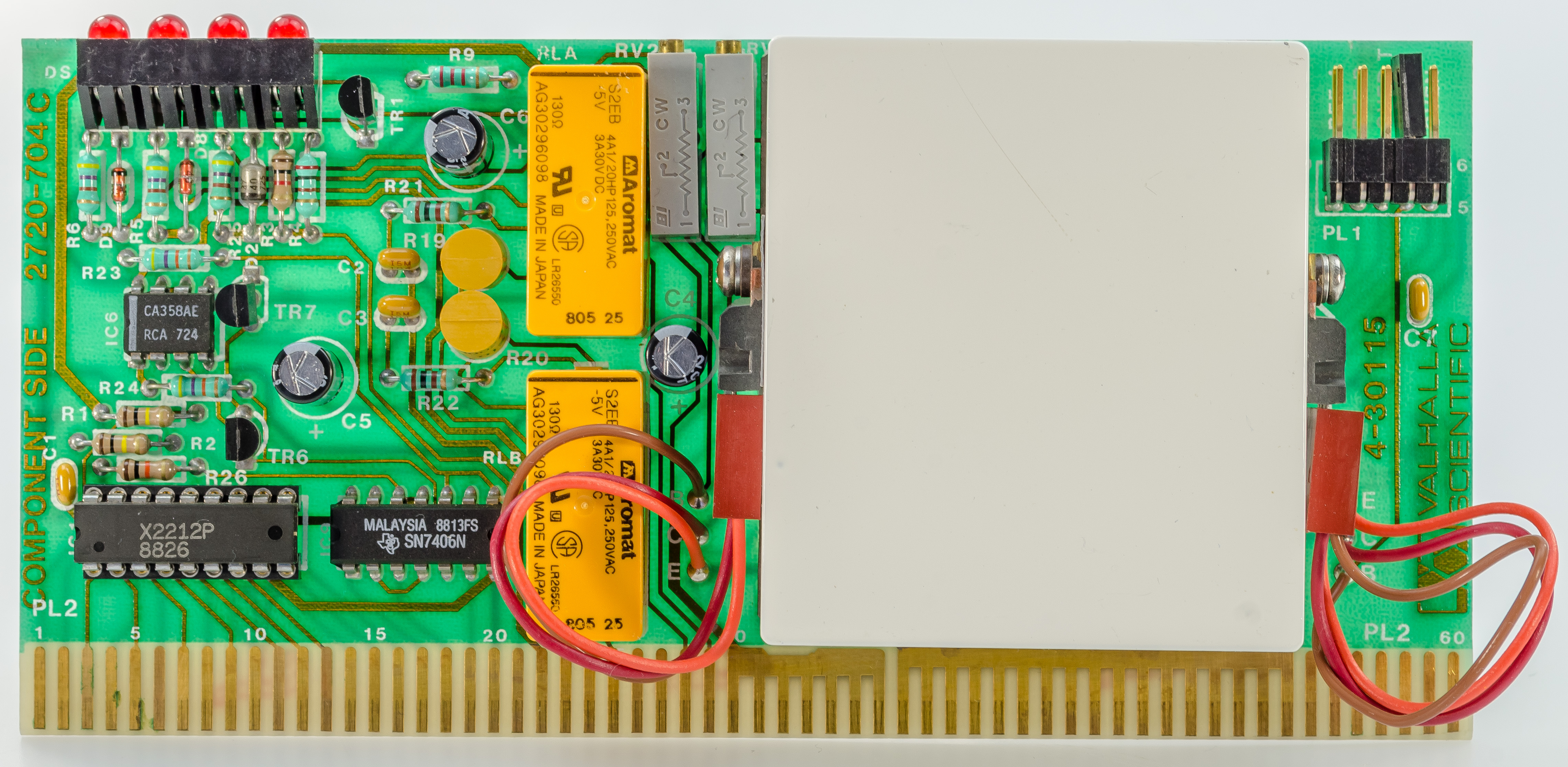
Null meter PCBA has amplifier stage with ICL7652 and LF356 and precision wirewound resistor network R22-R26. Relays RLD and RLE select desired gain of this amplifier. Analog output signal is converted into frequency by pretty expensive AD537 voltage to frequency converter and supplied to digital brains of the instrument via HCPL-2601 optoisolator.
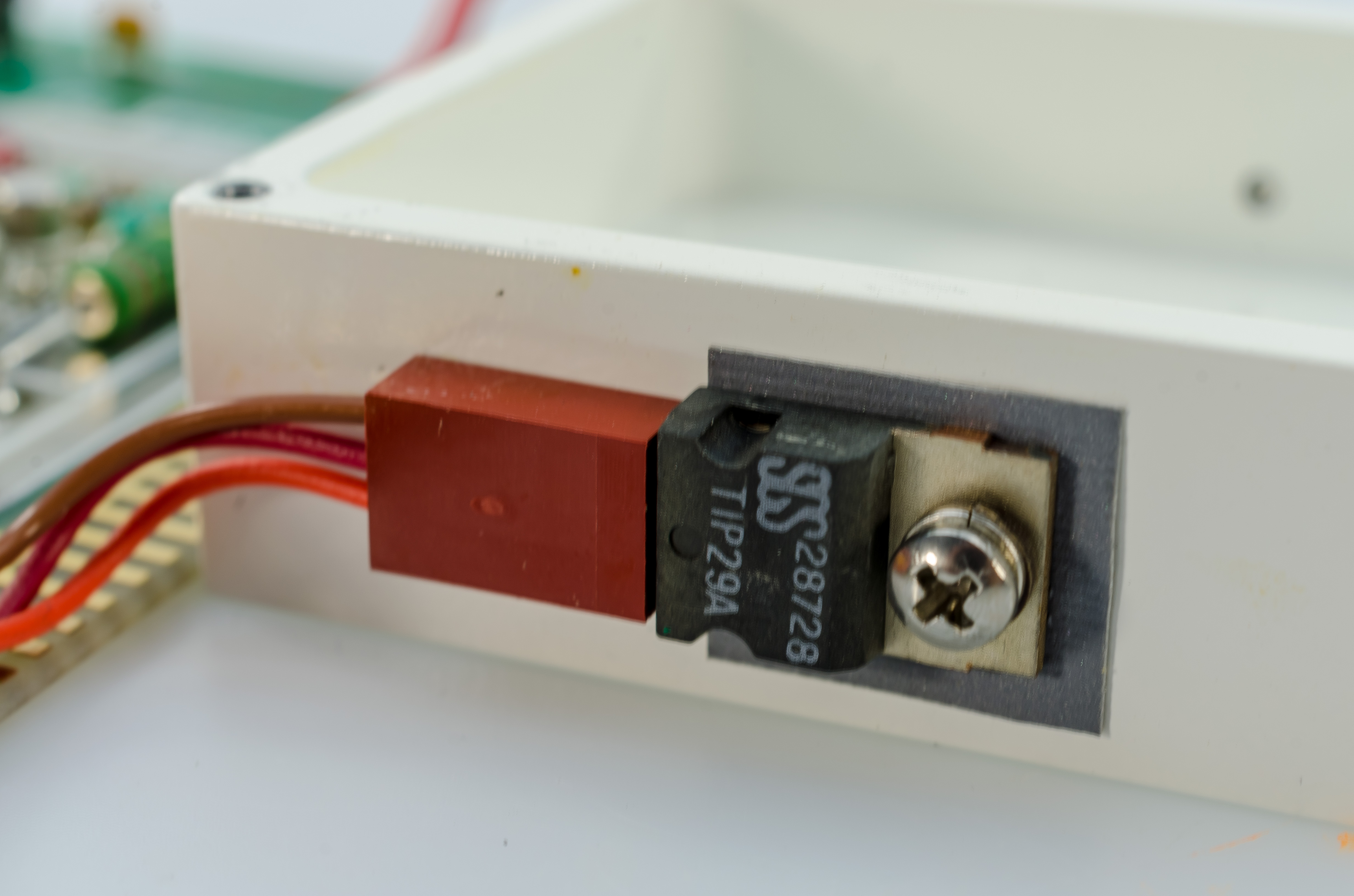
All this powered by fully isolated floating DC-DC power supply, based around Burr-Brown 722 module. This module has particularly interesting specifications with less than 1 µA of leakage current and 8000V isolation voltage rating. Internal transformer is driven at 900 kHz frequency, making it relatively easy to filter for clean output. Like many integrated solutions from 80s this components is quite expensive today, around $270 USD/piece on Digikey.
Mainboard and transformers, chassis parts
Firmware backups
Firmware 27C256, 61.61 2720GS version, Intel HEX-file
Firmware 27C256, 61.61 2720GS version, binary dump file
Reference 1 ×2212P dump binary
Reference 2 ×2212P dump binary
Reference 3 ×2212P dump binary
Internal CAL Data IC204 ×2212P dump binary
Internal CAL Data IC203 ×2212P dump binary
Error data, IC202 ×2212P dump binary
Divider data, IC201 ×2212P dump binary
Null-meter data, IC101 ×2210P dump binary
The moment of truth, first power up
The transformer was installed to the instrument and all connections recreated as intended. Some cable ties later and eventually everything was ready for the first power-up. Once both displays showed “Hi there” it was clear, this repair was a success.
The firmware revision showed 61.61 during boot sequence. Afterwards, all checks and self-tests passed without errors. “Last Cal” showed 9999 days for the internal reference and 8486 days for the internal divider, which leads to the impression the unit was never calibrated and still has the factory constants.
Performance verification tests
The first question that arises is, what about the internal references, if they haven’t been calibrated for multiple years?
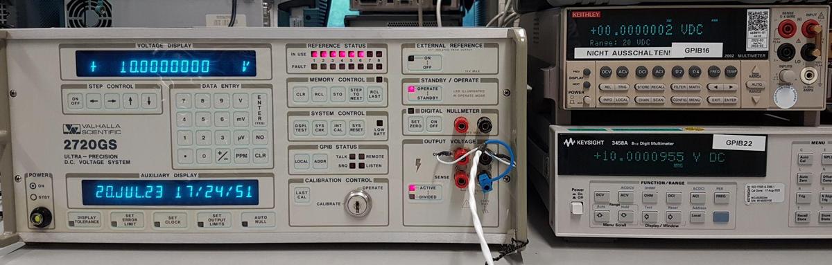
To answer that question a long scale Keysight 3458A DMM was used, that hasn’t seen any calibration for a year. So we need to figure out what to expect. Based on the calibration points for +10 V and -10 V and the resulting correction factors estimated from measured and expected value in the calibration reports, we now assume a linear drift for them and use a linear regression to estimate the new correction factor at the time of this measurement.
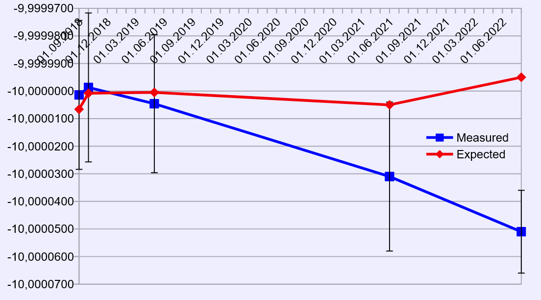
Next a set of 3 voltage references was measured with same Keysight 3458A in both polarities, consequently taking 16 measurements, corrected with the new correction factor for drift and finally TEMF compensated. Such correction was required because this particular Keysight 3458A meter was never ran with adjustment procedure (CAL 0, CAL 10, CAL 10kΩ).
Afterwards, the measurement was performed with Valhalla 2720GS in the way the manual suggests.
From here we can calculate the difference between both instruments and find that they agree to <2 µV/V.
| K3458A positive | K3458A positive corrected | K3458A negative | K3458A negative corrected | TEMF removed | Valhalla 2720GS | Δ K3458A-Valhalla 2720GS, V |
|---|---|---|---|---|---|---|
| 10.0087241 (std. 110 nV) | 10.0086621 | -10.0087259 (std. 179 nV) | -10.0086699 | 10.0086660 | 10,0086499 (std. 357 nV) | 16.07 µV |
| 10.0088423 (std. 169 nV) | 10.0087803 | -10.0088445 (std. 229 nV) | -10.0087884 | 10.0087844 | 10,0087683 (std. 425 nV) | 16.08 µV |
| 9.9899700 (std. 141 nV) | 9.9899081 | -9.9899718 (std. 238 nV) | -9.9899158 | 9.9899120 | 9,9898941 (std. 295 nV) | 17.84 µV |
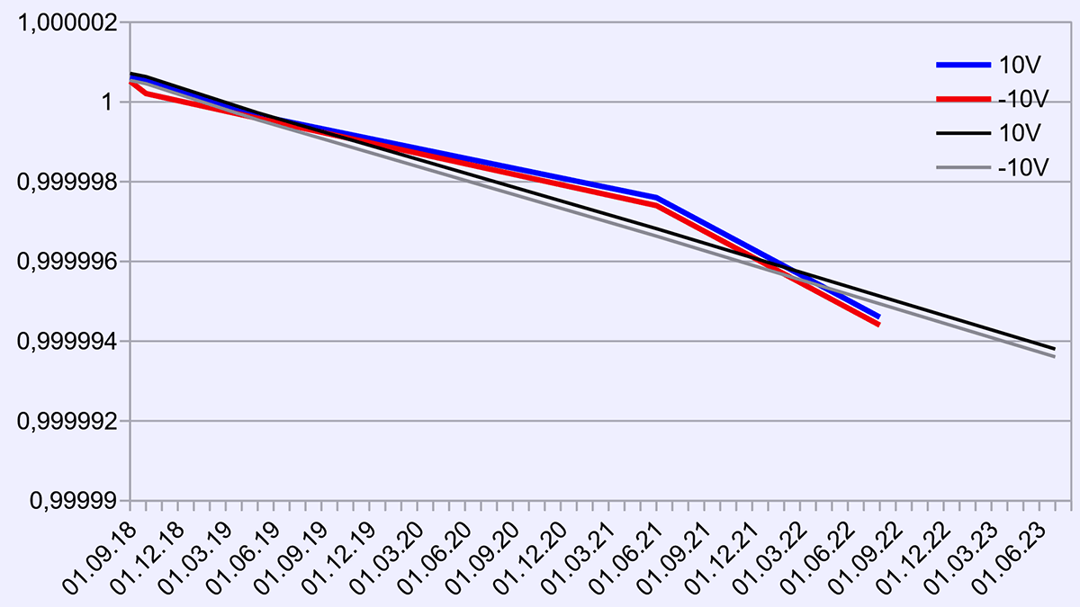
Furthermore, the output of the 2720GS at 10 V was measured with 3458A and the following values found:
| K3458A positive | K3458A positive corrected | K3458A negative | K3458A negative corrected | K3458A corrected & EMF removed |
|---|---|---|---|---|
| 10.0000801 V (std. 1,75 µV) | 10.0000181 V | -10.0000825 V (std. 1.49 µV) | -10.0000265 V | 10.0000223 V |
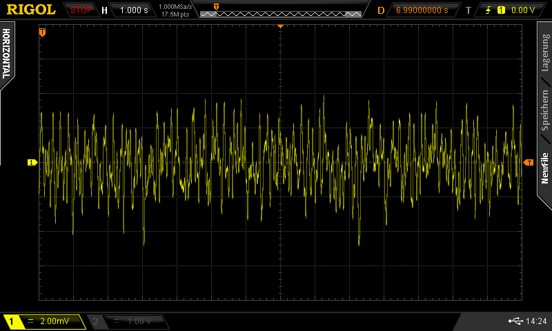
Next, the 0.1 … 10 Hz noise of the 10 V output was measured. We can spot about 8-9 µVpp.
Even if that frequency range is not specified we can assume the unit to be well within spec noise-wise (Wideband Noise 10 Hz to 10 kHz 30 µV RMS; add 20µV RMS for loads greater than 10mA).
Update from February 2025, new ovenized reference board replacement copy
The voltage reference board was reverse-engineered and redrawn in an ECAD software.
Figure 1: Layout for the reference board copy
Below is the full schematic of the reference board including the Gerber files for fabrication.
Figure 2: Schematics of the reference board (click for high resolution)
Board specs are rather common standard type, 2-layer FR-4 with green solder mask and ENIG plating (for edge contacts reliability purposes).
Gerbers ZIP-archive for reference PCB
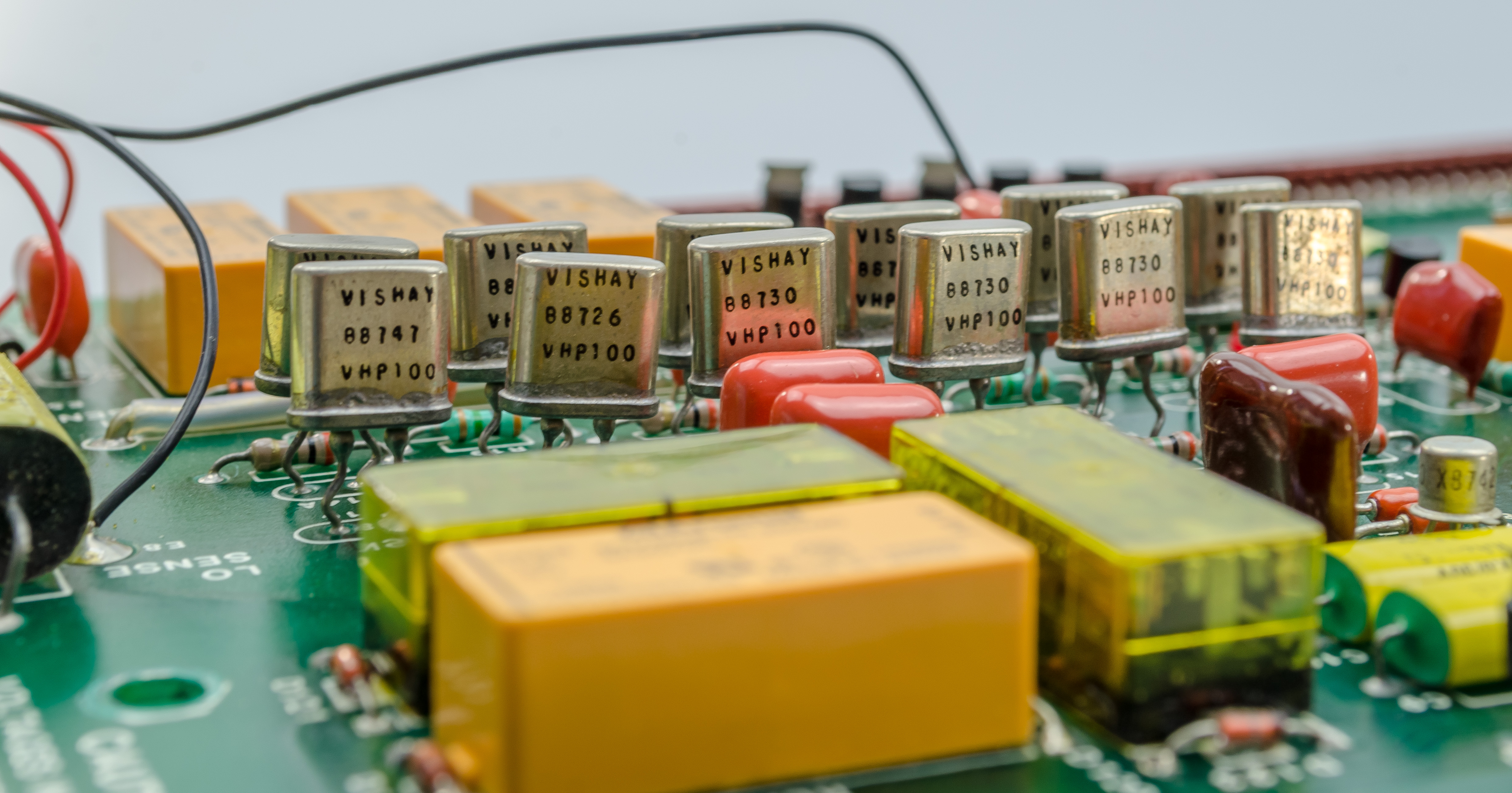
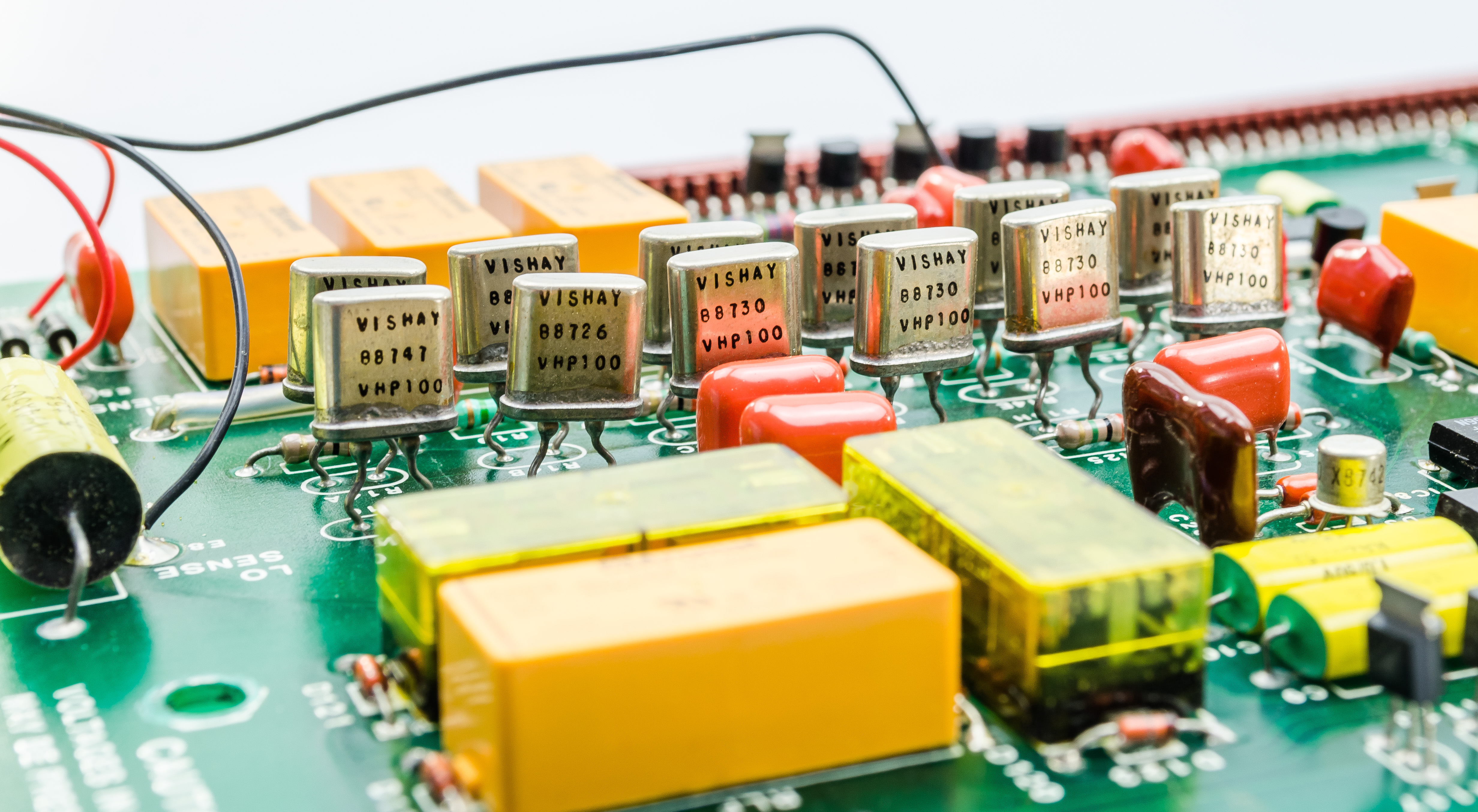
Components such as X2212P (MBM2212 or CAT22C10), AD590JH (2-Terminal IC Temperature Transducer), 2N4392 (N-Channel JFET), 2N4402 (N-Channel JFET) and P1087 (P-Channel JFET) acquired at the surplus market allowed a complete replication of the board as shown in the image below. For the 10 kΩ resistors at the reference outputs Neohm UWP50 was used. All other components were bought from Mouser.
Thanks to a six pack of beer, the oven housing was manufactured at work by a colleague.
Figure 3: Copycat of the reference board for 2720GS
Figure 4: Comparison of the copycat (top far) to the original Valhalla board (bottom front)
The reference was initially populated with two LM399 and added to the instrument with an empty NVRAM chip fitted to the board plus the oven adjusted according to the manual:
“This adjustment is only required following component replacement in the oven control circuitry on the REFERENCE MODULE PCB”.
Note: 2720GS with serial numbers prior to 20-127 only have one adjustment and no test point connector – contact Valhalla Scientific for details if an early reference module requires adjustment.
- Remove option “BAT” or “EBU” (if fitted) and the Ac power. Allow Valhalla 2720GS to fully cool for at least 8 hours with the top cover and the REFERENCE SYSTEM COVER removed.
- Remove the shorting link from all reference PCB test connectors and the test connector at the rear top edge of the OUTPUT SYSTEM PCB.
- Apply AC power with the POWER switch in the STBY position.
- Monitor the voltage between pins 5 V (+) and 6 V (-) on the respective PCBs’ test connector (front top edge) with a voltmeter with an accuracy of better than 0.01 V at 0.5 VDC.
- Adjust RV1 for a reading of 0.5 ±0.05 VDC on the voltmeter. Note that if the ambient temperature is not 20 °C then this voltage should be decreased by 0.02 V per °C above 20 °C. The user should also note that the “HEATING” LED on the reference PCB should be illuminated at this time.
- Monitor the voltage between pins 3 V (+) and 8 V (~) on the test connector with the above voltmeter.
- Adjust RV2 for a reading of 0.1 V more than that obtained in step e) above.”
Unfortunately, the instrument didn’t like the new reference board at first. The most likely explanation is, that the selected LM399 were too far off from the average voltage. Hence, a batch of Analog Devices ADR1399KHZ, that were way closer to the average voltage, were selected and populated on the board. Turns out, the instrument accepted the board afterwards without any complains. Thus, the rest of the references were replaced with ADR1399KHZ, too. All of them were selected by their reference voltage being close to each other and the instrument accepted all of them and set them all into use. The table below shows the situation before, during and after the modifications.
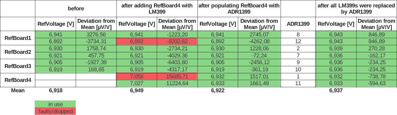
Table 1: Voltage reference selection
After a warm-up time, the instrument was adjusted using external 10 V, 1 V and a 100 Ω standards.
- 10 V calibration – 2720GS “learns” the absolute volt
- 1 V calibration – Used with the 10 V step to “learn” voltage ratio
- Ammeter Calibration – calibrates the internal ammeter (required every 3 years)
- The user should note that the only “required” calibrations are that of 10 V, 1 V and the ammeter.
- Ammeter Calibration … required connection to a 100 Ω 0.1% tolerance resistor
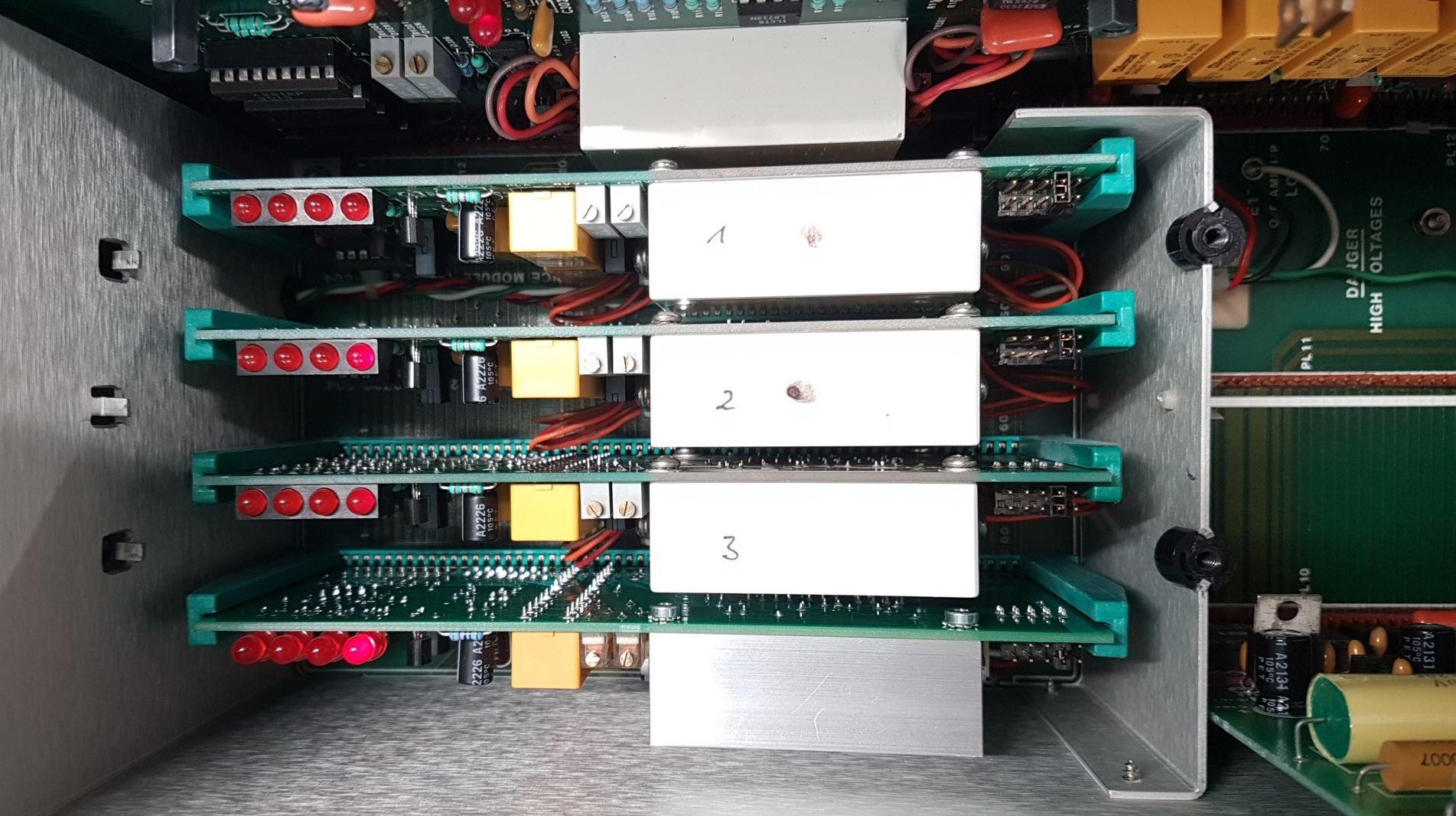
Figure 5: New reference board populated in slot 4 of the instrument
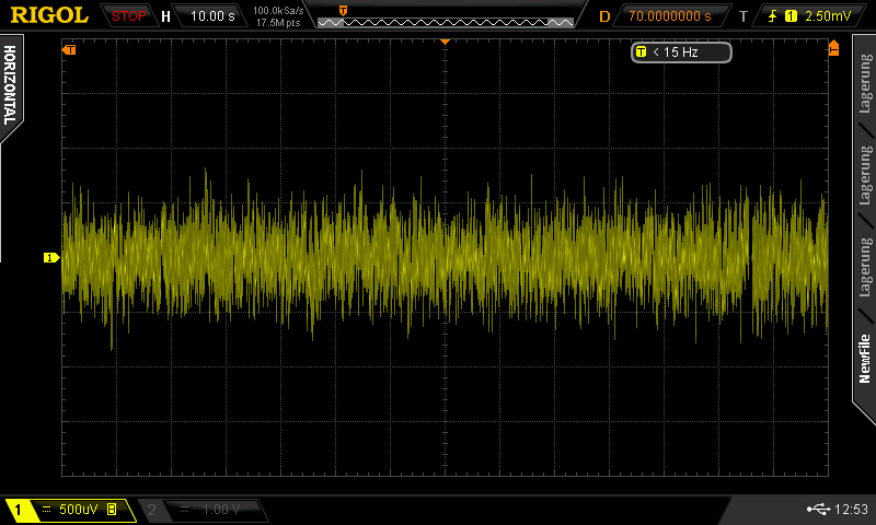
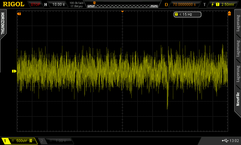
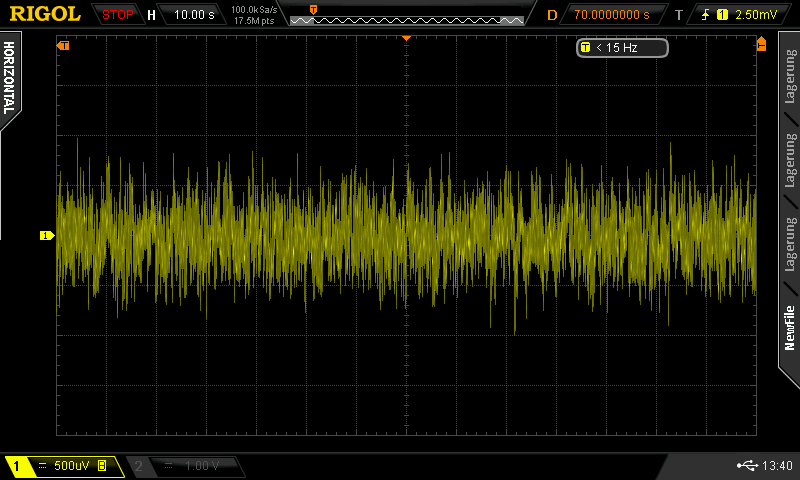
Next, a noise measurement was performed. Some 2.3 Hz and 12 Hz hum is visible in the noise. The source was first unknown, but expected to come from the oven controllers on the reference board.
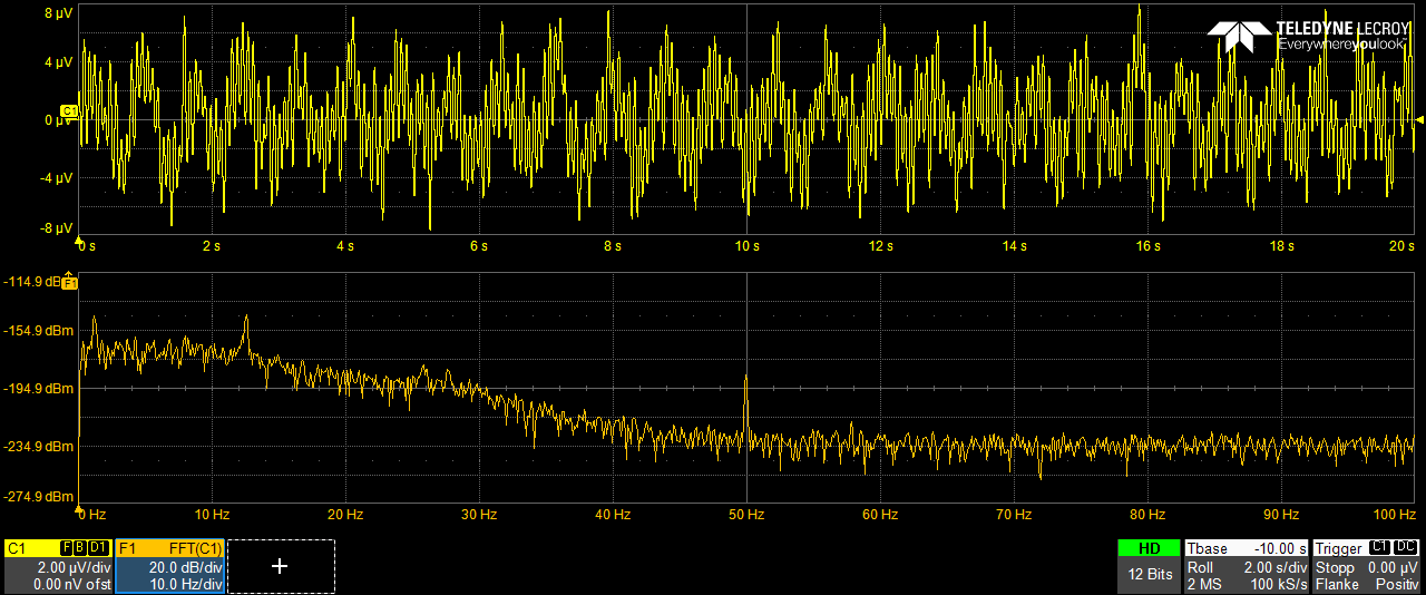
Figure 6: Output noise measurement at 10 V output, 2 s/div resolution
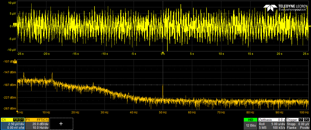
Figure 7: Output noise measurement at 10 V output, 5 s/div resolution
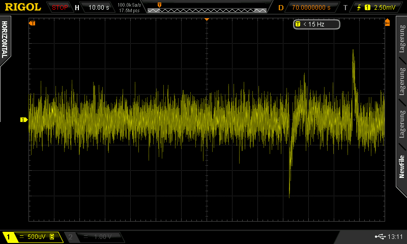
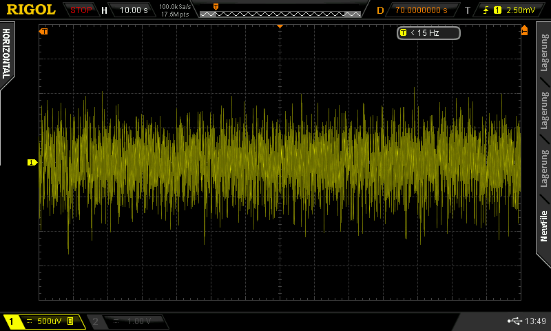
The service manual indicated, that in some board revision C7 was added across R10 = 10 MΩ. None of the boards had this capacitor installed. Page 27 of the service manual revealed a 1 µF capacitor across the 10 MΩ of the output system oven controller.
Eventually, 1 µF/50V X7R 0805 caps between pin 1 and 2 of the corresponding opamps on all of the boards were added and the oscillation vanished.
However, noise is still far off from the theoretical 500 nVpp that one would expect from 8 x ADR1399 averaged output.
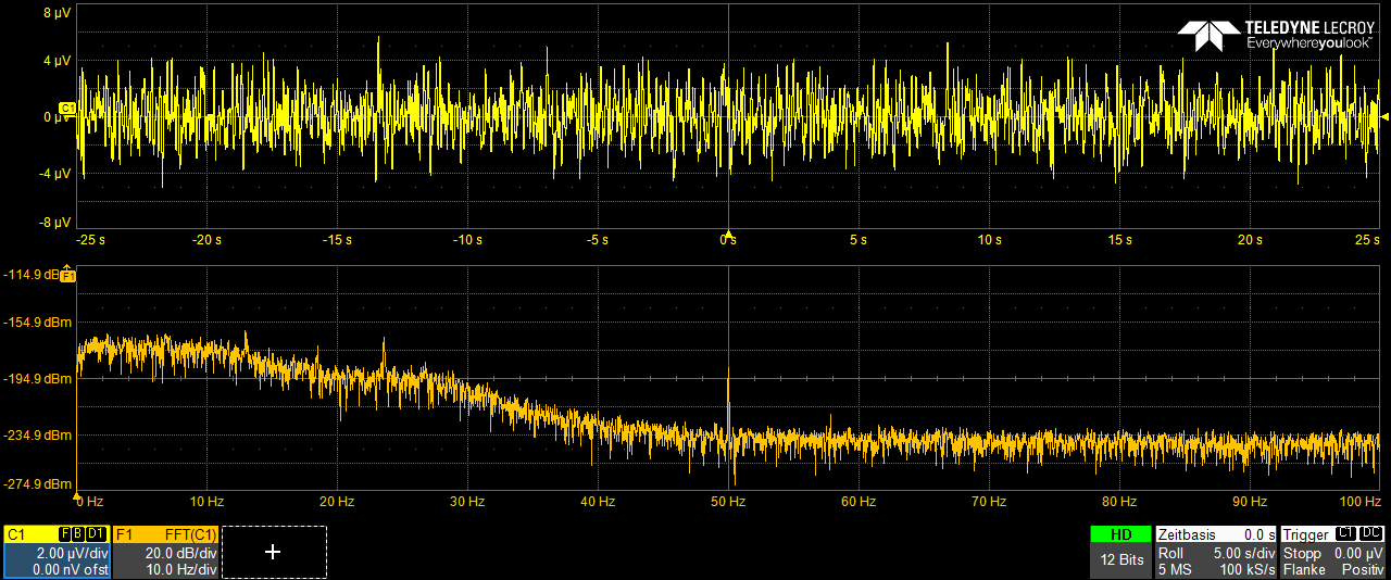
Figure 8: Output noise measurement at 10 V output after adding C7 to the REF PCBA, 5 s/div
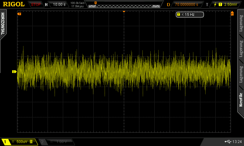
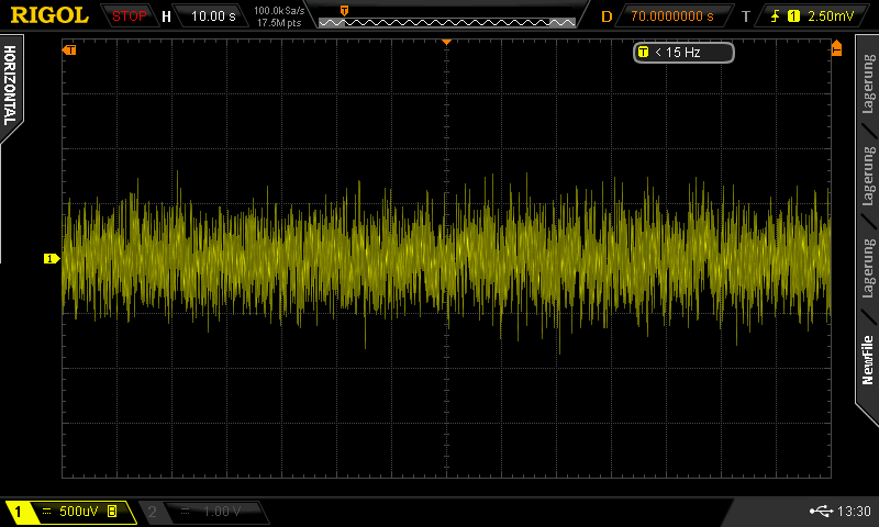
Next, noise of all reference boards were measured individually to spot if the output noise is due to the reference boards or the electronics that follows. This way it was found that reference 2a exhibits popcorn noise.
Replace µV by nV in the below images to obtain accurate numbers after external LNA.
| Ref | Noise measurement 1 (click for details) | Noise measurement 2 (click for details) |
|---|---|---|
| 1a | 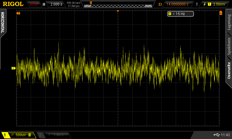 |
 |
| 1b | 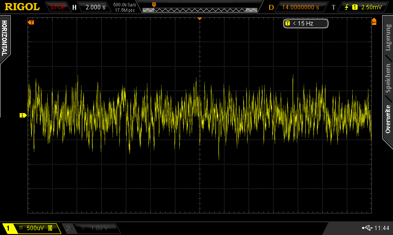 |
 |
| 2a | 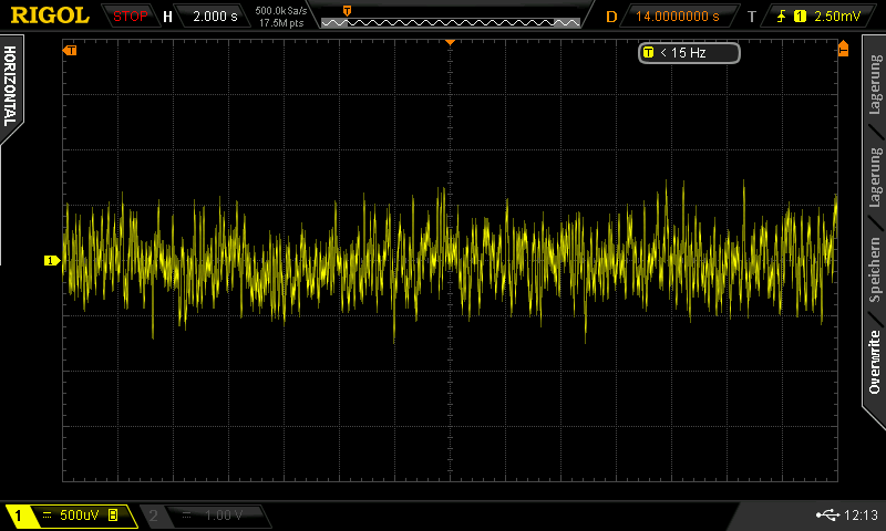 |
 |
| 2b | 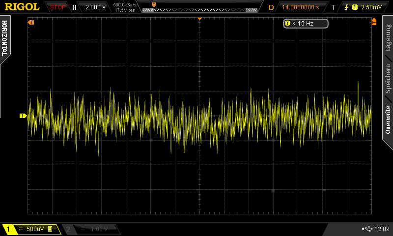 |
 |
| 3a | 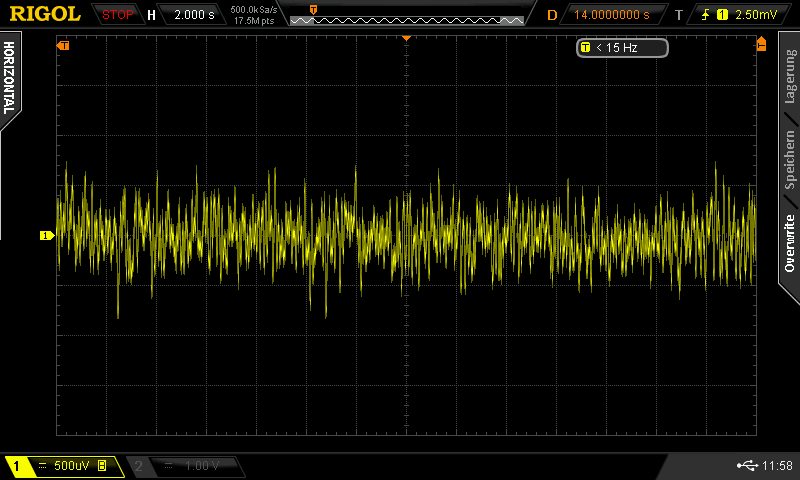 |
 |
| 3b | 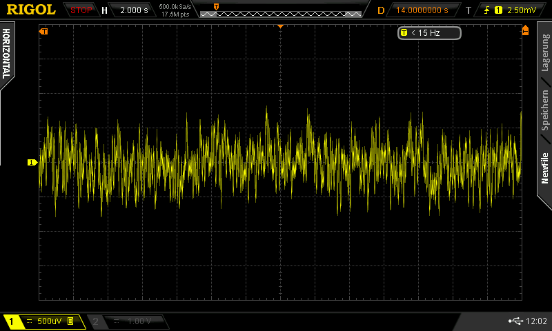 |
 |
| 4a | 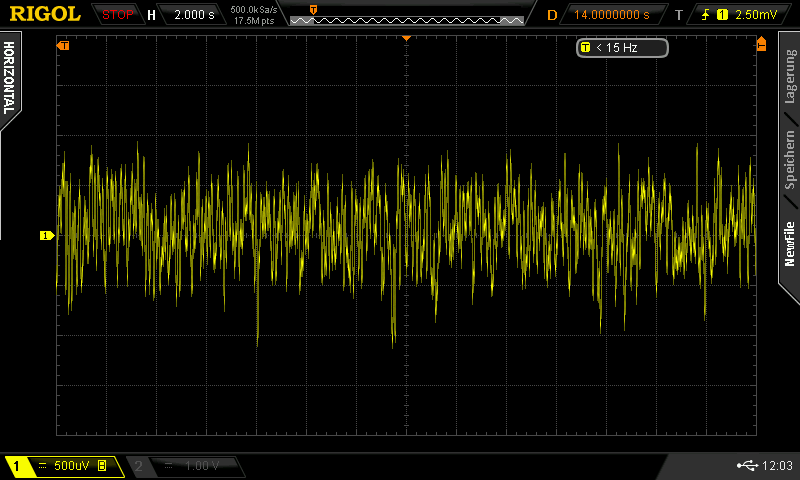 |
 |
| 4b | 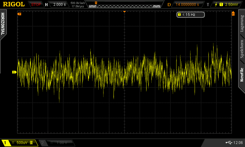 |
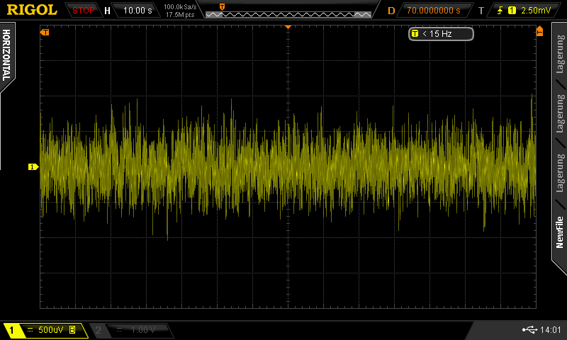 |
Table 2: Noise measurements of each reference zener
Lowering the value of the summing resistors at the reference outputs to 1 kΩ did not change anything in the overall noise.
Replacing some of the chopper amps in the following signal chain with more modern choppers made things worse and also led to oscillations. That in contrast could lead to the conclusion, that the source of the noise must be found elsewhere outside of the reference card, such as the main 2720GS PWMDAC and its filter.
Linearity measurement
Next, linearity was measured against a reference HP 3458A. “The linearity of the 2720GS is defined as the maximum allowable deviation from the straight line between zero and full scale of each range”, which indicates an endpoint INL definition.
| Range | Linearity | Linearity, relative to a range |
|---|---|---|
| 650 mV | 0.14 µV | 0.22 µV/V |
| 1300 mV | 0.26 µV | 0.20 µV/V |
| 0.65 V | 0.22 µV | 0.34 µV/V |
| 1.3 V | 0.32 µV | 0.25 µV/V |
| 6.5 V | 0.9 µV | 0.14 µV/V |
| 13 V | 1.8 µV | 0.14 µV/V |
| 65 V | 10 µV | 0.15 µV/V |
| 130 V | 18 µV | 0.14 µV/V |
| 600 V | 85 µV | 0.14 µV/V |
| 1200 V | 165 µV | 0.14 µV/V |
Table 3: Linearity specification of Valhalla 2720
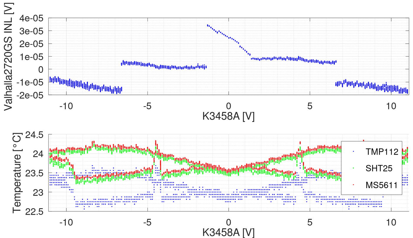
Figure 9: Linearity sweep from -11 V to +11 V relative to HP3458A
The first result showed, that the instrument switches ranges and can not be forced to stay within a fixed range to get a reading at 0 V. One can easily spot the 13 V, 6.5 V, 1.3 V and 0.650 V ranges.
So the different ranges have to be handled separately for analysis, which is part of future work.
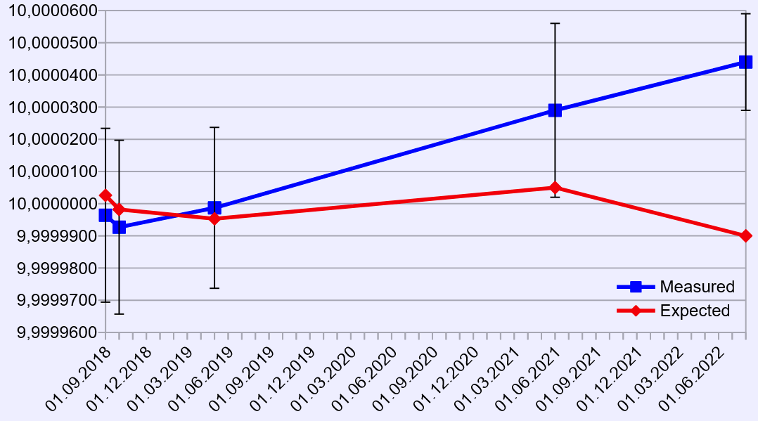
Long-term stability study
Long-term stability measurements were performed also with the HP3458A. This study revealed, that the output was unstable over time and the air-condition in the lab did not made things better. Huge temperature excursion over a single day were observed and some of the reference boards were switched off every now and then.
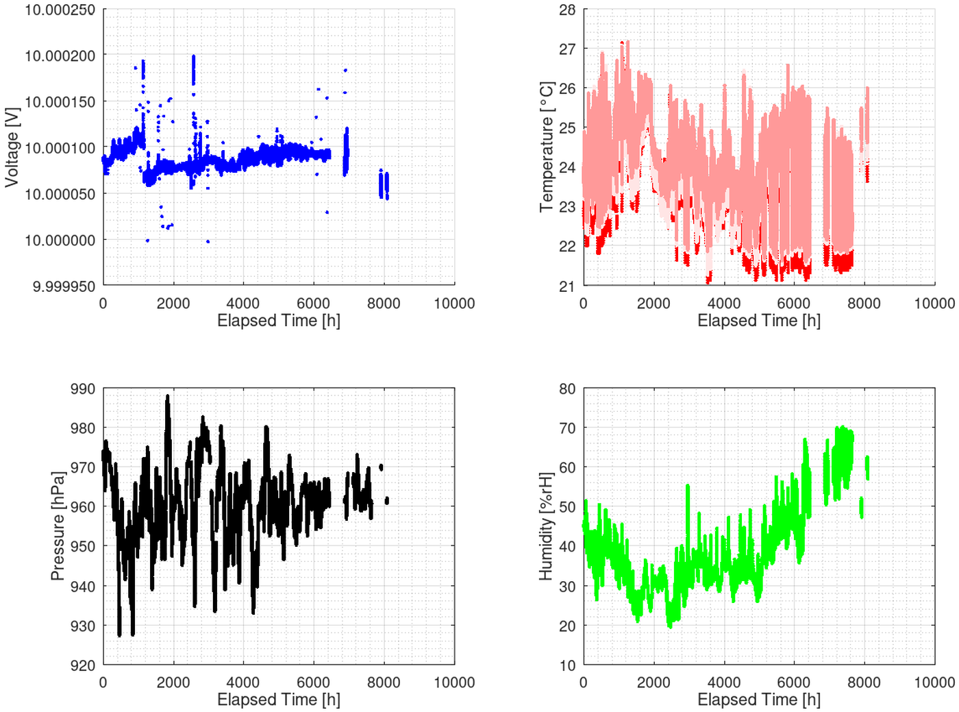
Figure 10: Long-term stability measurement with all ovens set according to manual
Hence why the outlets of the air-condition in the lab were rearranged and the five oven temperatures of the voltage reference boards and resistor inside the unit lowered to 45 °C. The over temperature alarm signals were adjusted accordingly and a new long term measurement was started.
This improved stability, but additional adjustment of the alarm signal was needed several times, most likely due to settling of components within the oven. The 10 V output now appears to be stable over the last 1000 hours.
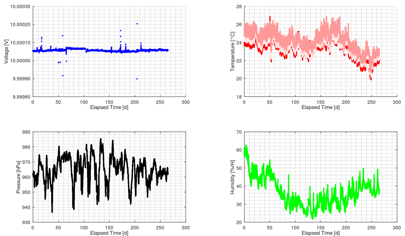
Figure 11: Long-term stability measurement after decreasing all ovens to +45 °C
Extra goodies: The secret password
By the way, it was K. Weber who found the secret password for the instrument in August 2023 by reverse engineering the firmware, its 2560021258.
..to be continued..
Projects like this are born from passion and a desire to share how things work. Education is the foundation of a healthy society - especially important in today's volatile world. xDevs began as a personal project notepad in Kherson, Ukraine back in 2008 and has grown with support of passionate readers just like you. There are no (and never will be) any ads, sponsors or shareholders behind xDevs.com, just a commitment to inspire and help learning. If you are in a position to help others like us, please consider supporting xDevs.com’s home-country Ukraine in its defense of freedom to speak, freedom to live in peace and freedom to choose their way. You can use official site to support Ukraine – United24 or Help99. Every cent counts.
Modified: June 7, 2025, 12:30 p.m.