Draft
Contents
- Intro
- Documentation
- Teardown and construction review
- Raspberry Pi software to control Keithley 7168
- DIY scanner controller
- Leakage test
- Voltage offset test
- Results and summary
Introduction
The Model 7168 is an 8-channel, 2-pole card with <30nV of thermal offset. It will switch any one of eight signals to one output in less than 3ms. Channel offset leakage current is <50pA at 23°C. When the 7168 is used with the Model 2182A nV-meter, the noise and drift performance of the 2182A is not degraded.
| Feature | Model 7168 spec | Model 2182A spec |
|---|---|---|
| Channels | 8 | 2 |
| Configuration | Two Poles Per Channel, Input Hi And Lo | |
| Connector Type | Screw Terminal To Bare Copper PCB | Custom LEMO connector |
| Max. Signal Level | 10VDC, 50mA Peak (Resistive Load Only) | 110% of range, up to 110V |
| Contact Resistance | < 12Ω | N/A |
| Contact Potential (Hi To Lo) Between Channels | <30nV with REL, copper cable; typ. <60nV w/o REL | N/A |
| Contact Type | JFET Switch | N/A |
| Actuation Time | ≪3ms, Exclusive Of Mainframe | N/A |
| Input Leakage | <50pA/ch at 23°C | <50pA/ch at 23°C |
| Input Isolation | >109 Ω, <40 pF | >109 Ω, <1500 pF |
| Common Mode Voltage | 30 VPEAK | 150 VPEAK |
| Maximum Voltage Between Any Two Terminals | 10 V | 70 VPEAK |
| Warm-Up for thermal stability | 2 Hours In Mainframe | 2.5 Hours |
| Operating Environment | 0°…40°C; Up To 35°C At 70% R.H. | =. 0°…50°C; Up To 35°C At 80% R.H. |
Table 1: Feature comparison
This card is designed for use in Keithley 705 and 706 switching mainframe unit. It’s also supported by modern Keithley 7001 and 7002 mainframes. However performance of this sensitive nV-scanner specified only for Model 705, due to presence of switching power supply in 700x units. We will test the impact of using SMPS in our DIY setup.
Documentation
Keithley Model 7168 Nanovolt Scanner Card datasheet
Keithley Model 7168 Nanovolt Scanner Card Instruction Manual, Sep.1991, Rev.C
Keithley Model 7168 Nanovolt Scanner Card old specification Rev.A
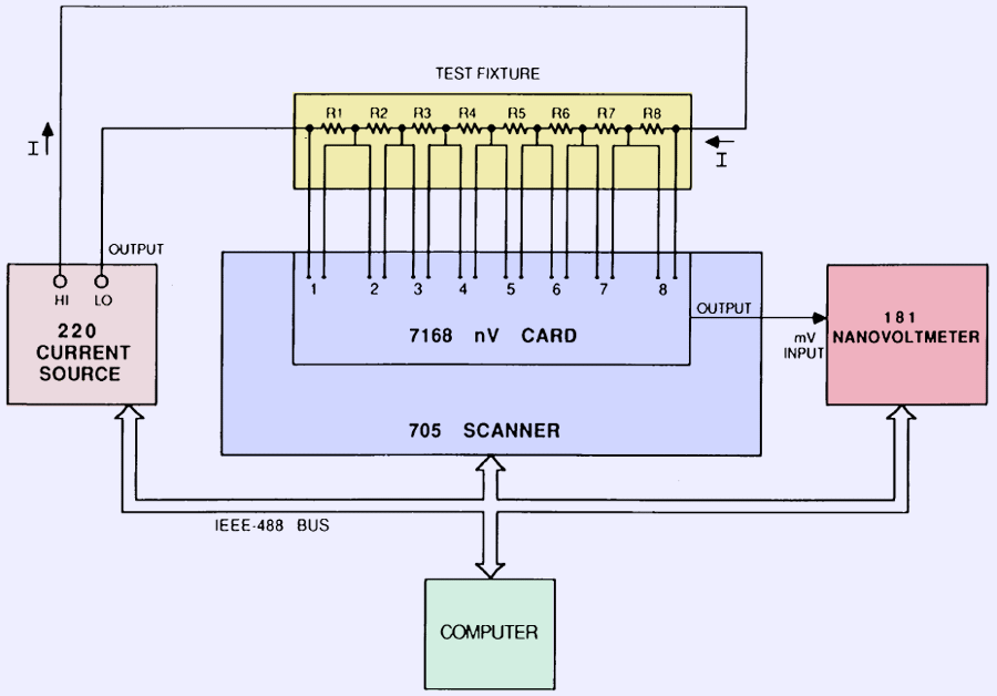
Test setup to be – Raspberry Pi as controller, EM A10 nanovolt amplifier as output head and 8½-digit DMM as digitizer.
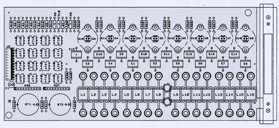
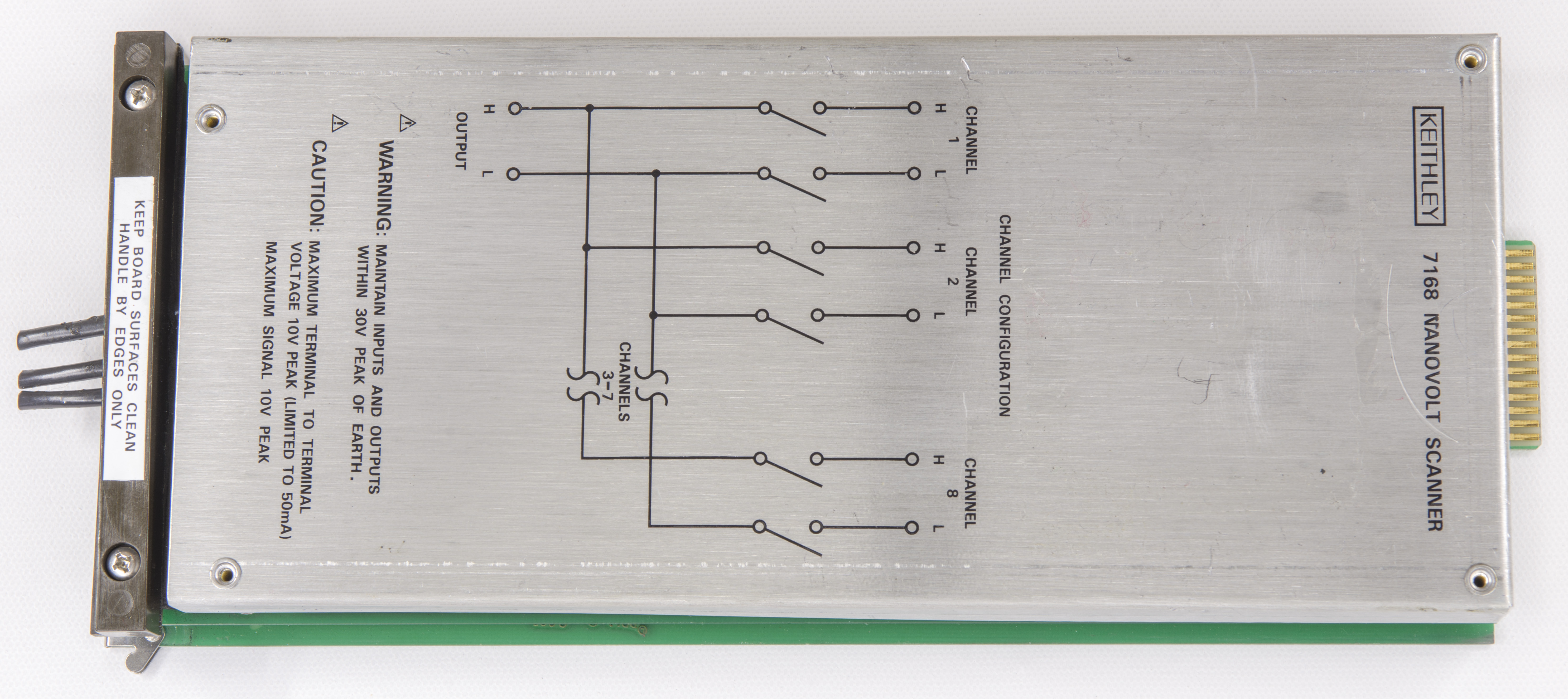
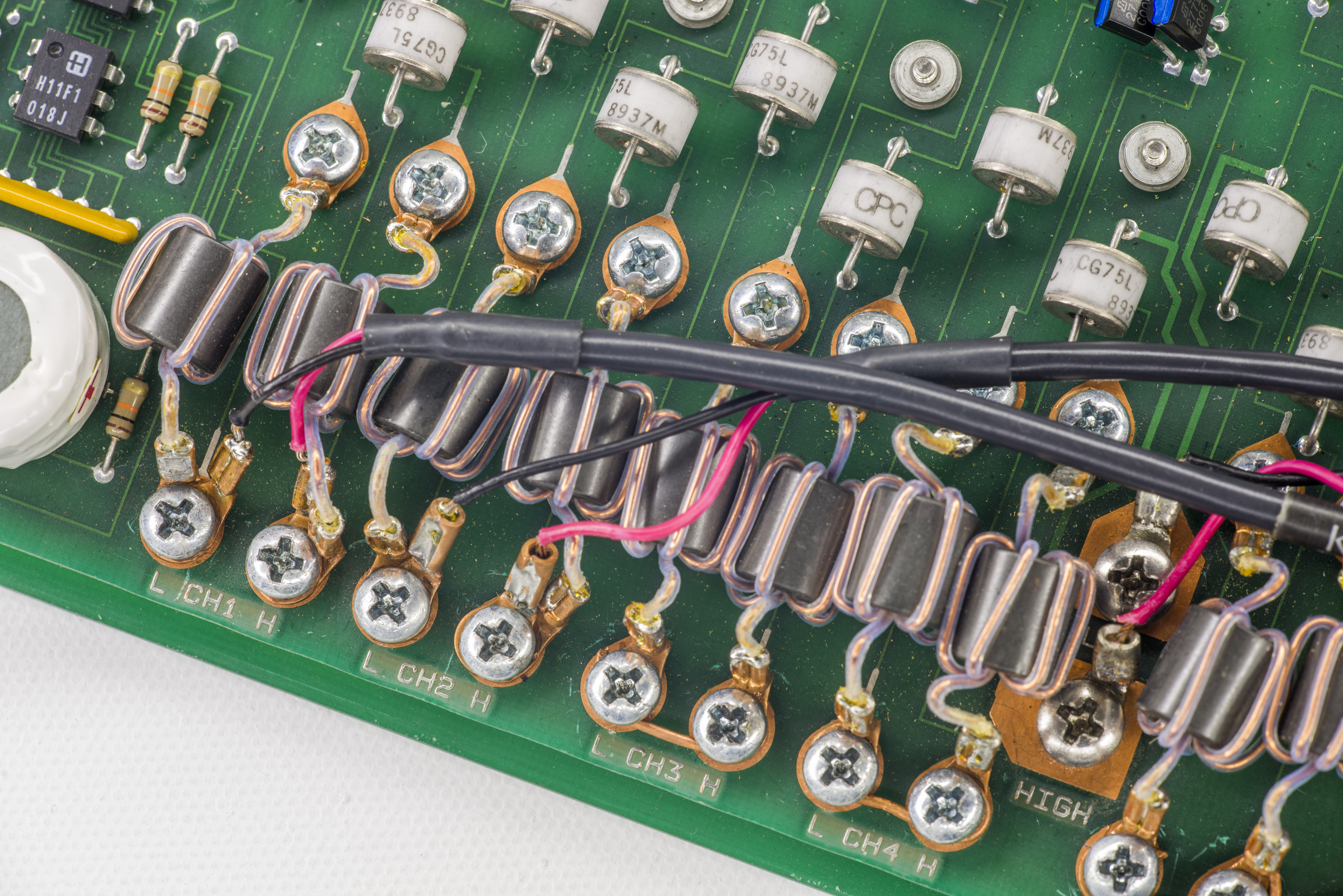
Image 1: Model 7168 nanovolt scanner card overview
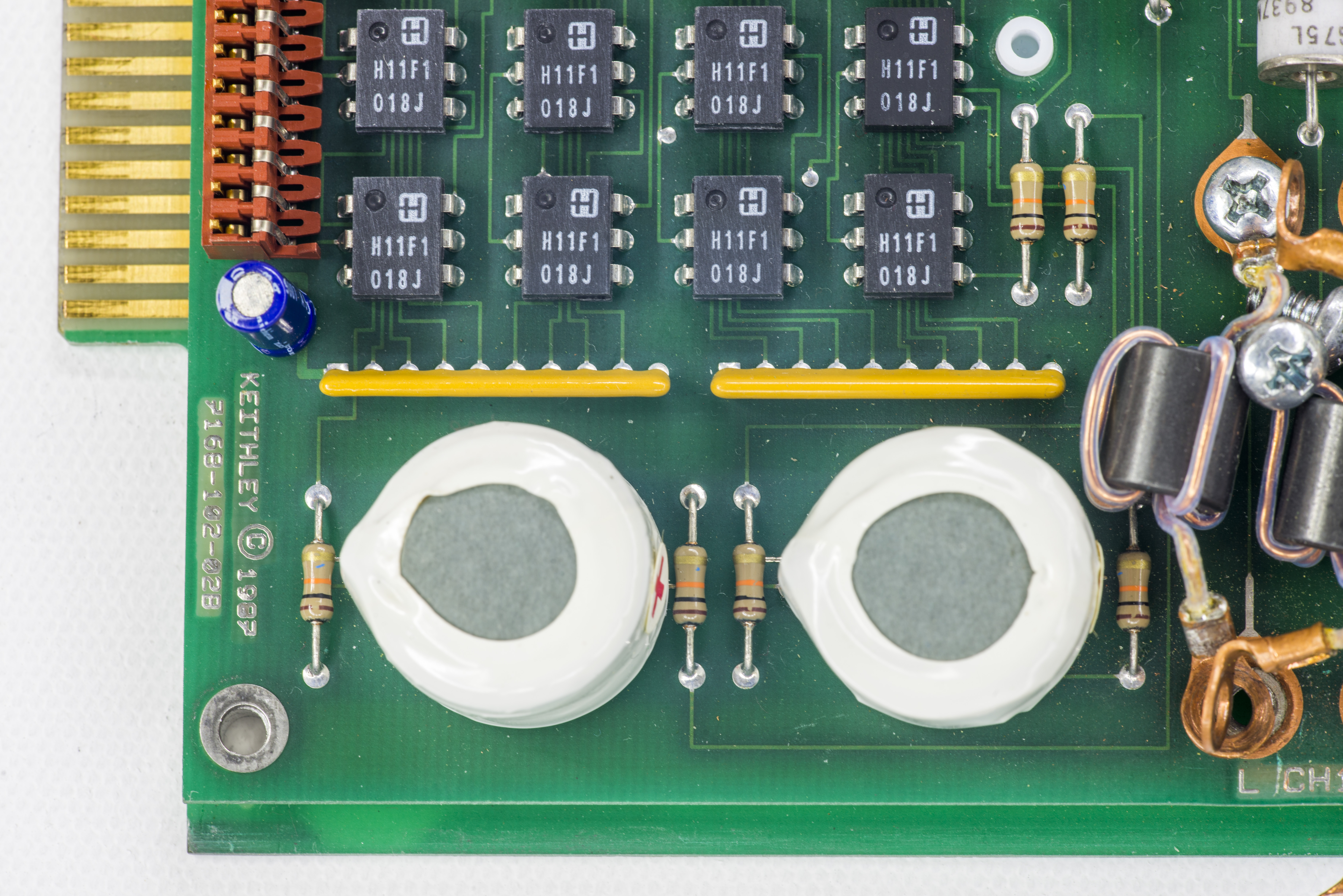
There are total eight inputs channels available for switching, with single output. Both HI and LO signal paths are routed symmetrical.
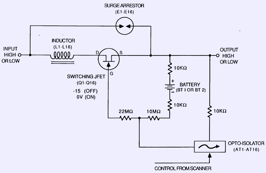
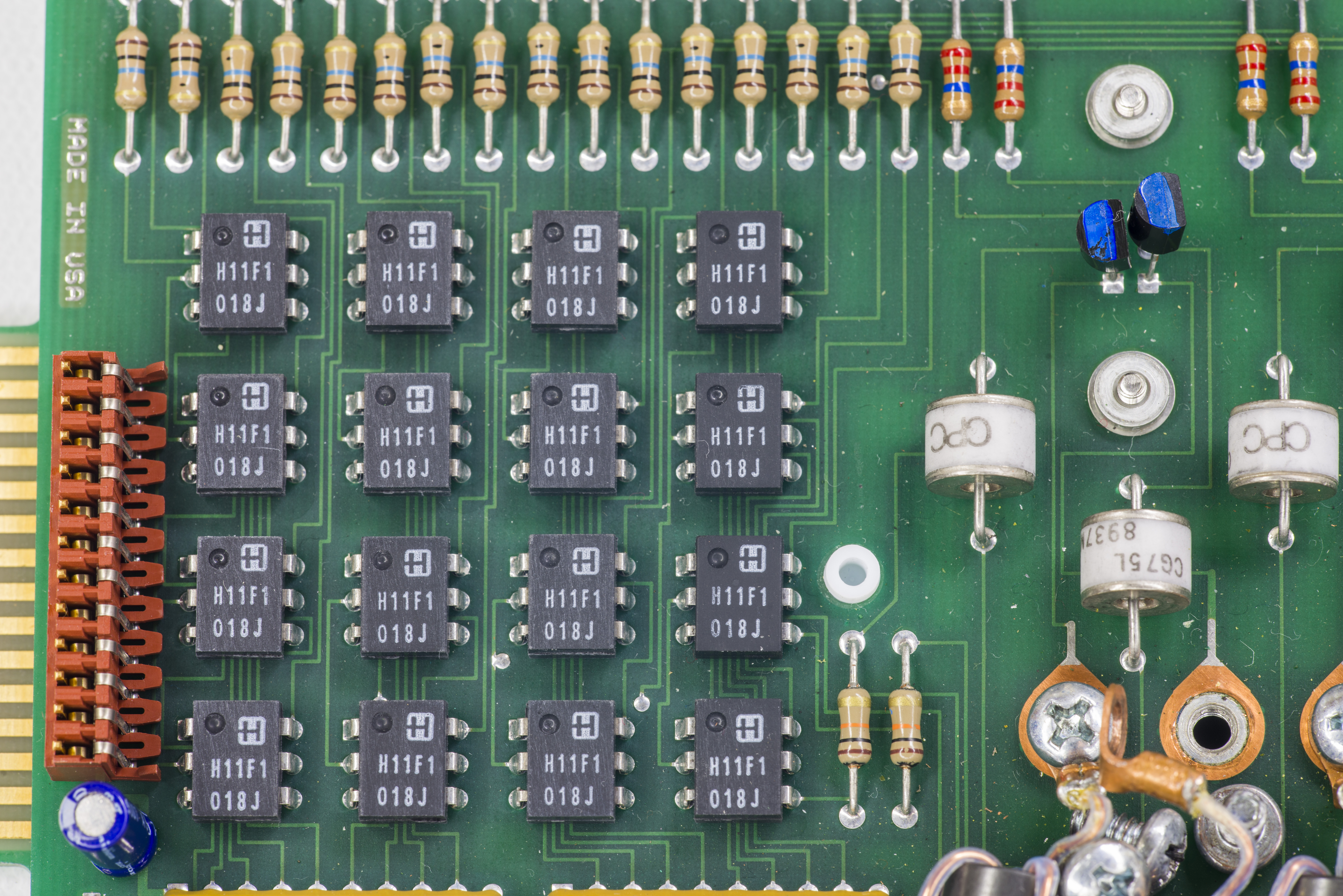
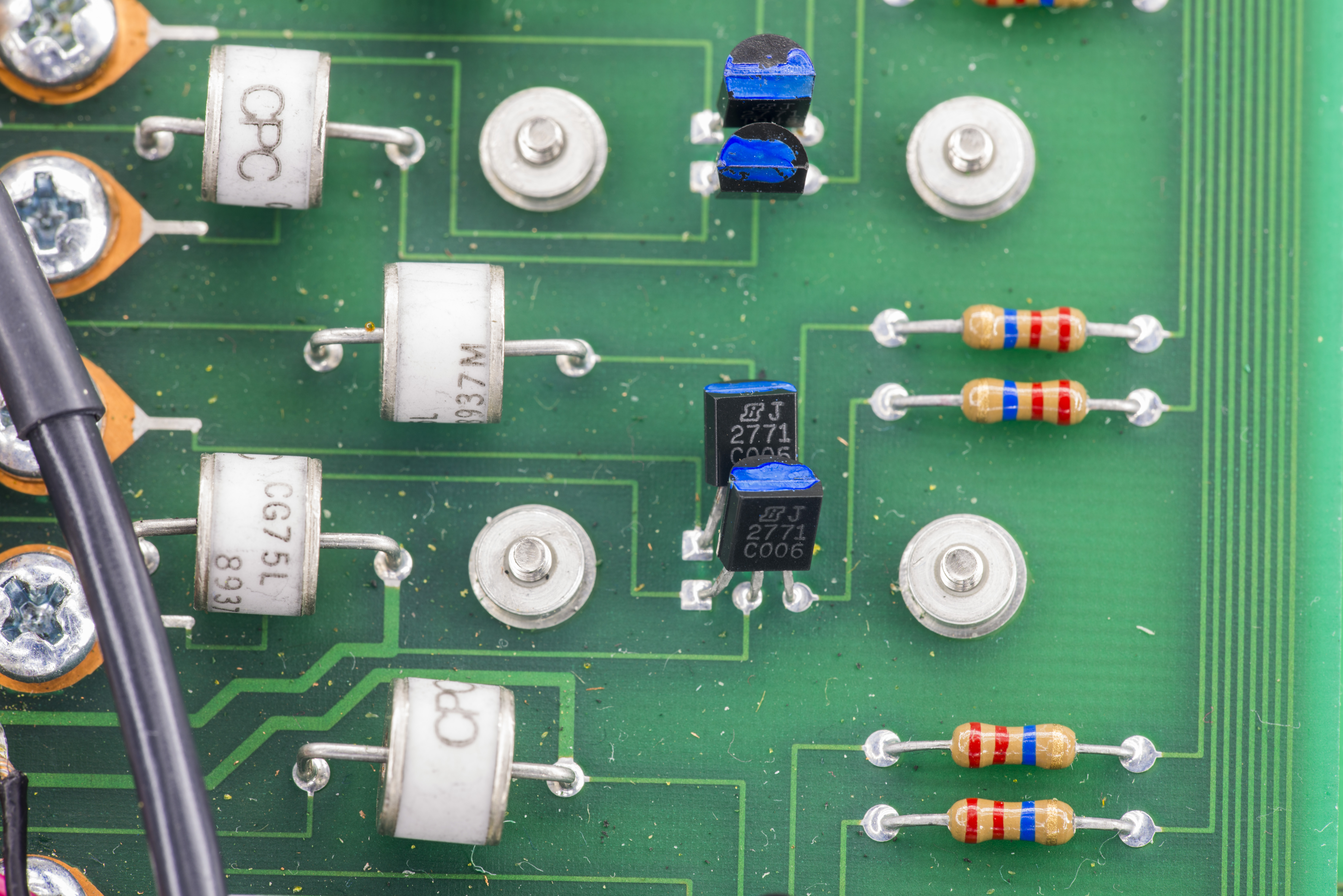
Image 2: Model 7168 channel design
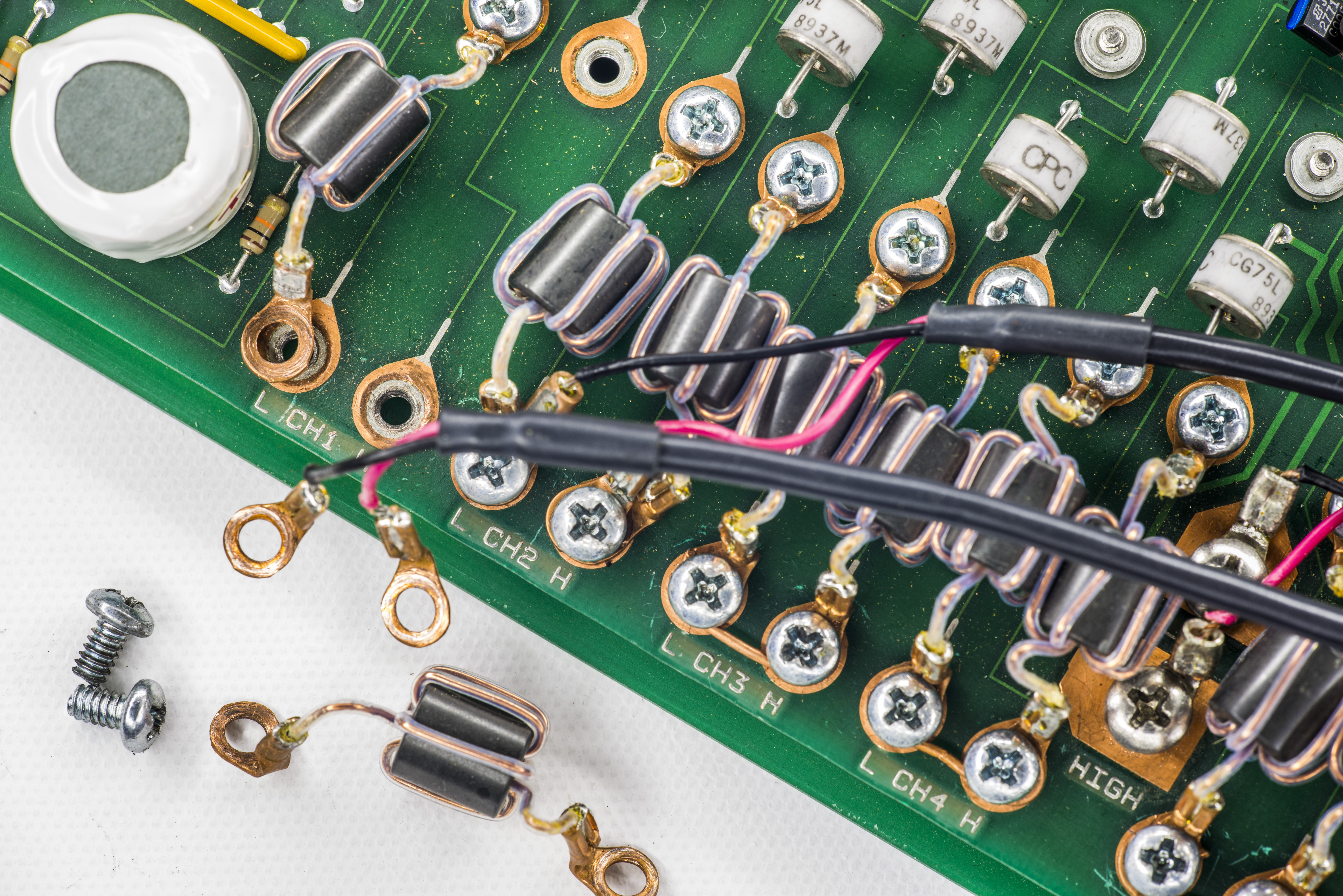
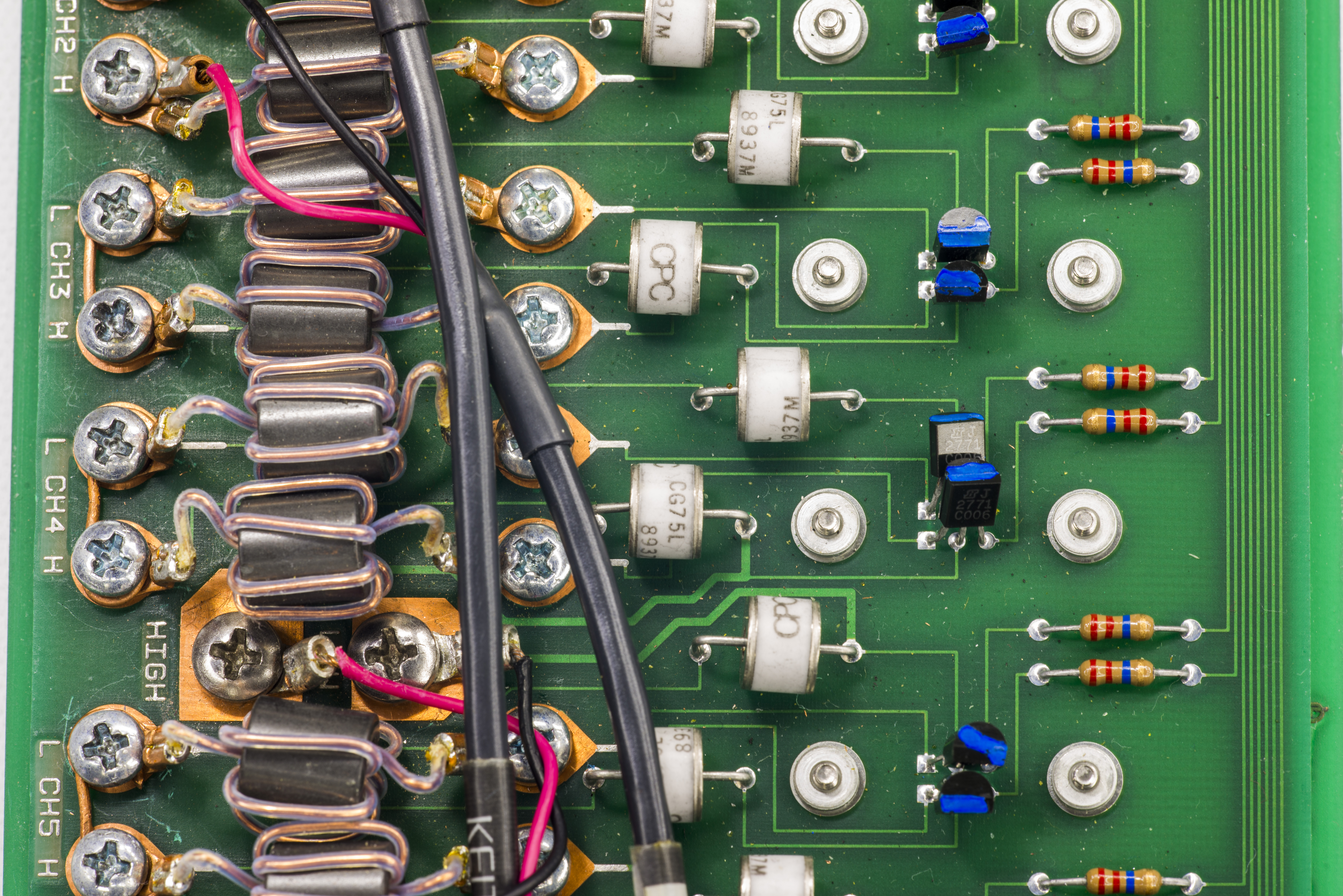
Both high and low sides of each channel are switched by N-channel JFETs Q1 to Q16. Channel is open (high-impedance) when JFET gate driven at negative -15 VDC and closed (low-resistance) when gate voltage is kept around 0 V, referenced to JFET source.
GDT surge arrestors E1-E16 in series with L1-16 inductors provide basic protection for JFETs. Isolation from controller realized with optocouplers AT1-AT16.
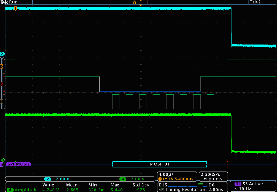
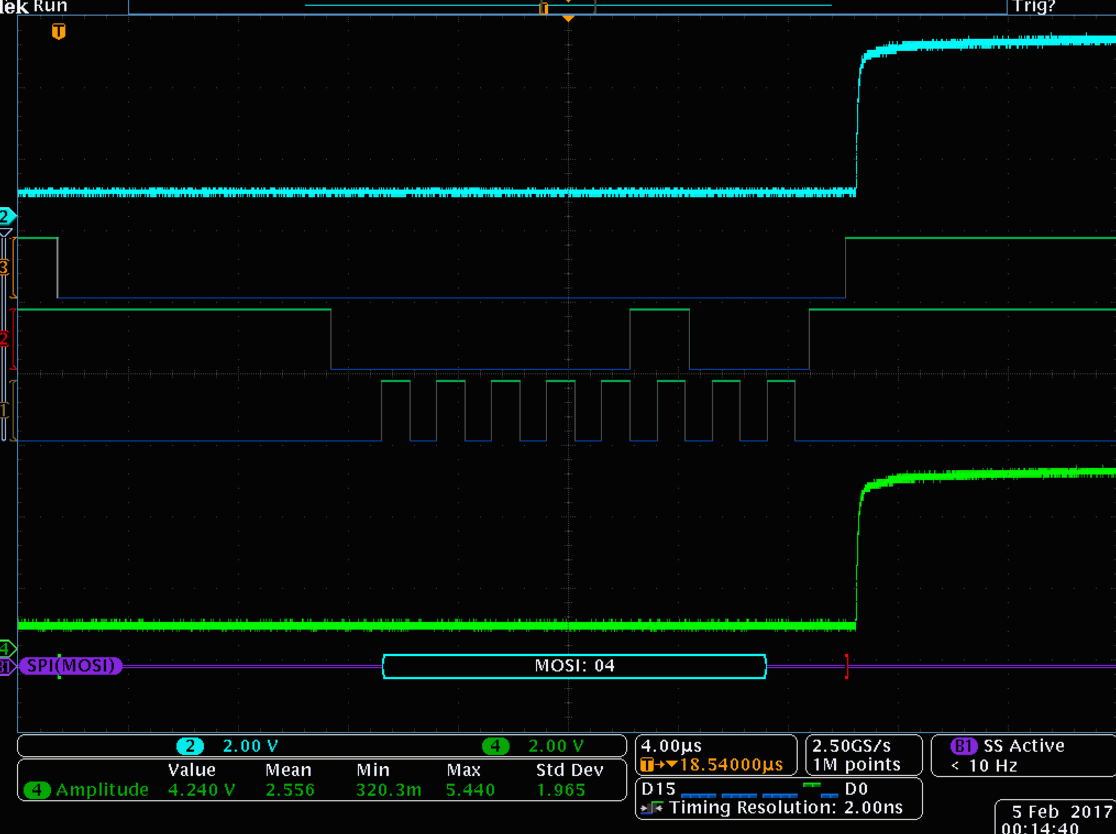
Multiple channels can be closed simultaneously, so pay attention during programming and configuration. It’s worth to test program code on “dry” runs without actual signals connected to card input channels.
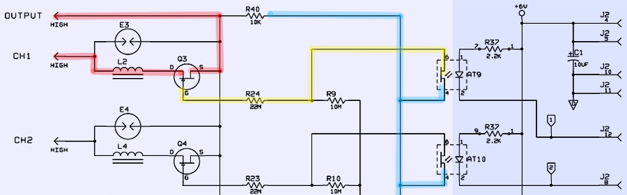
Image 3: Detailed schematics block for 2 channels
Dissimilar metals, in contact with each other, produce a small voltage. This voltage value depends on junction temperature and is therefore called a thermal EMF. The rate of change of this thermal EMF voltage with temperature is a function of the metals used in combination. The sense of the voltage produced is either positive or negative, depending on which side of the combination is being considered the input. Most, if not all electronic components, even simple resistors, capacitors, diodes have internal intermetallic combinations, and eventually connected to PCB/wire copper conductors as a final junction. Hence, copper is the typical reference metal in thermal EMF figures and analysis. Here are some examples of typical thermoelectric coefficients (also known as Seebeck coefficients) of bi-metal connections with copper.
| Material | Thermoelectric Potential (EMF) | Error magnitude on 1VDC with 5°C ΔT |
|---|---|---|
| Copper-Copper | < 0.2 µV/°C | <1 ppm |
| Copper-Silver | -0.3..+0.03 µV/°C | -1 ppm |
| Copper-Gold | +0.01..+0.2 µV/°C | +1 ppm |
| Copper-Cadmium/Tin | 0.3 µV/°C | 1.5 ppm |
| Copper-Lead/Tin | 1…3 µV/°C | 15 ppm |
| Copper-Zeranin | -1.3 µV/°C | -6.5 ppm |
| Copper-Brass | -1.6 µV/°C | -6.5 ppm |
| Copper-Evanohm | +2.0 µV/°C | +10 ppm |
| Copper-Manganin | -1.7..-3.0 µV/°C | -15 ppm |
| Copper-Aluminum | -4.0 µV/°C | -20 ppm |
| Copper-Nickel | -10..-22.0 µV/°C | -55..-110 ppm |
| Copper-Constantan | +39.7 µV/°C | -195 ppm |
| Copper-Kovar | 40 µV/°C | 200 ppm (0.02%) |
| Copper-Cupron | -45.0 µV/°C | -225 ppm |
| Copper-Silicon | 400 µV/°C | 0.2% |
| Copper-Copper Oxide | 1000 µV/°C | 0.5% |
Table 2: Typical thermal EMF figures with different metal junctions
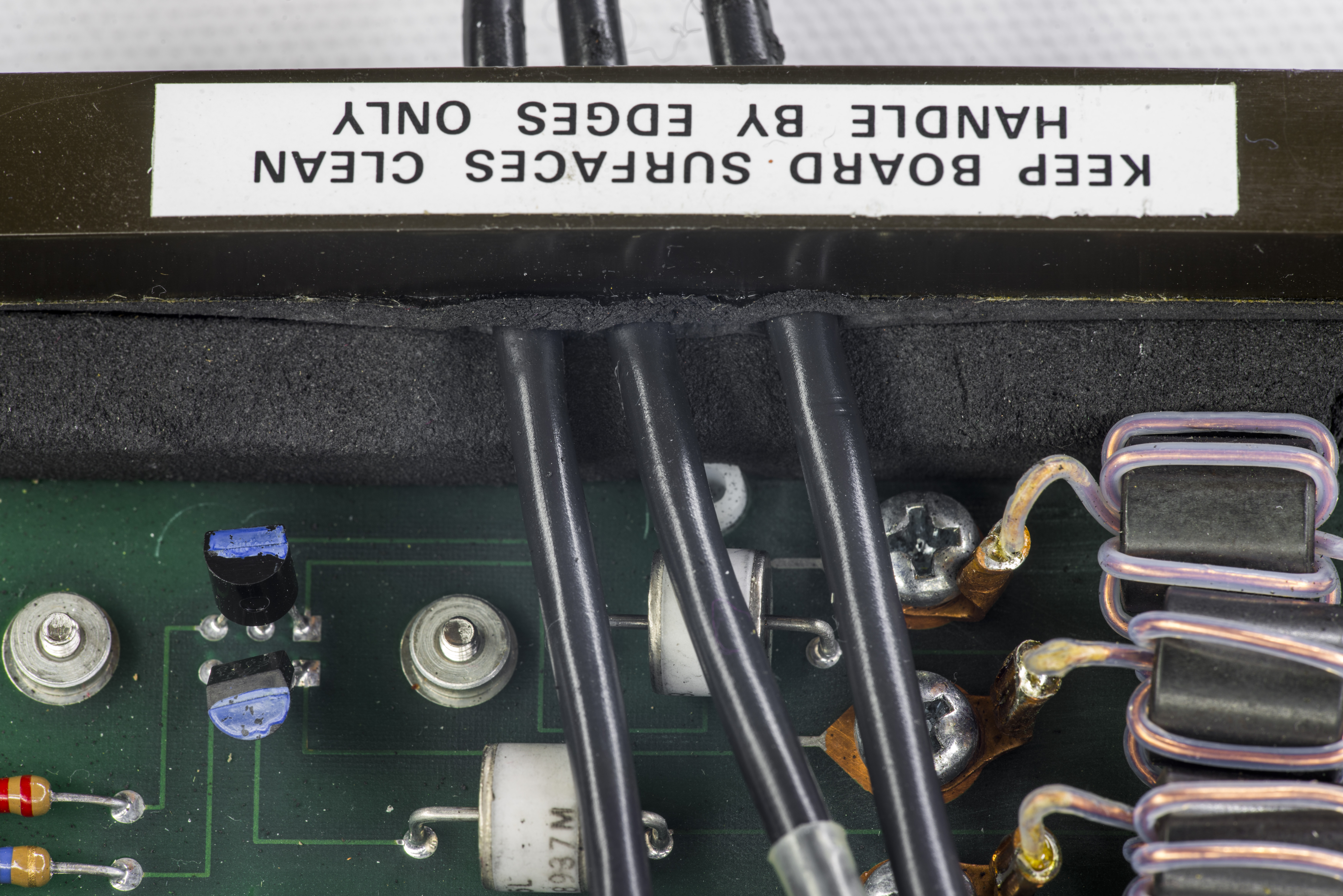
To minimize thermal offsets use only fresh clean copper wires and spade lugs. Do not solder connections to avoid dissimilar metals on contact area. Soldered connection can make parasitic offsets 1-3µV/°C, which is significant source of error for precision measurements. Make sure surfaces of copper contacts shiny, as copper oxide have very large thermal EMF. If copper oxidized, use soft abrasive pad to clean connections and attach wire immediately. Proper copper-copper connection have typical offset of 0.2 µV/°C or less, while oxidized/tinned connection can be more than 1000 µV/°C.
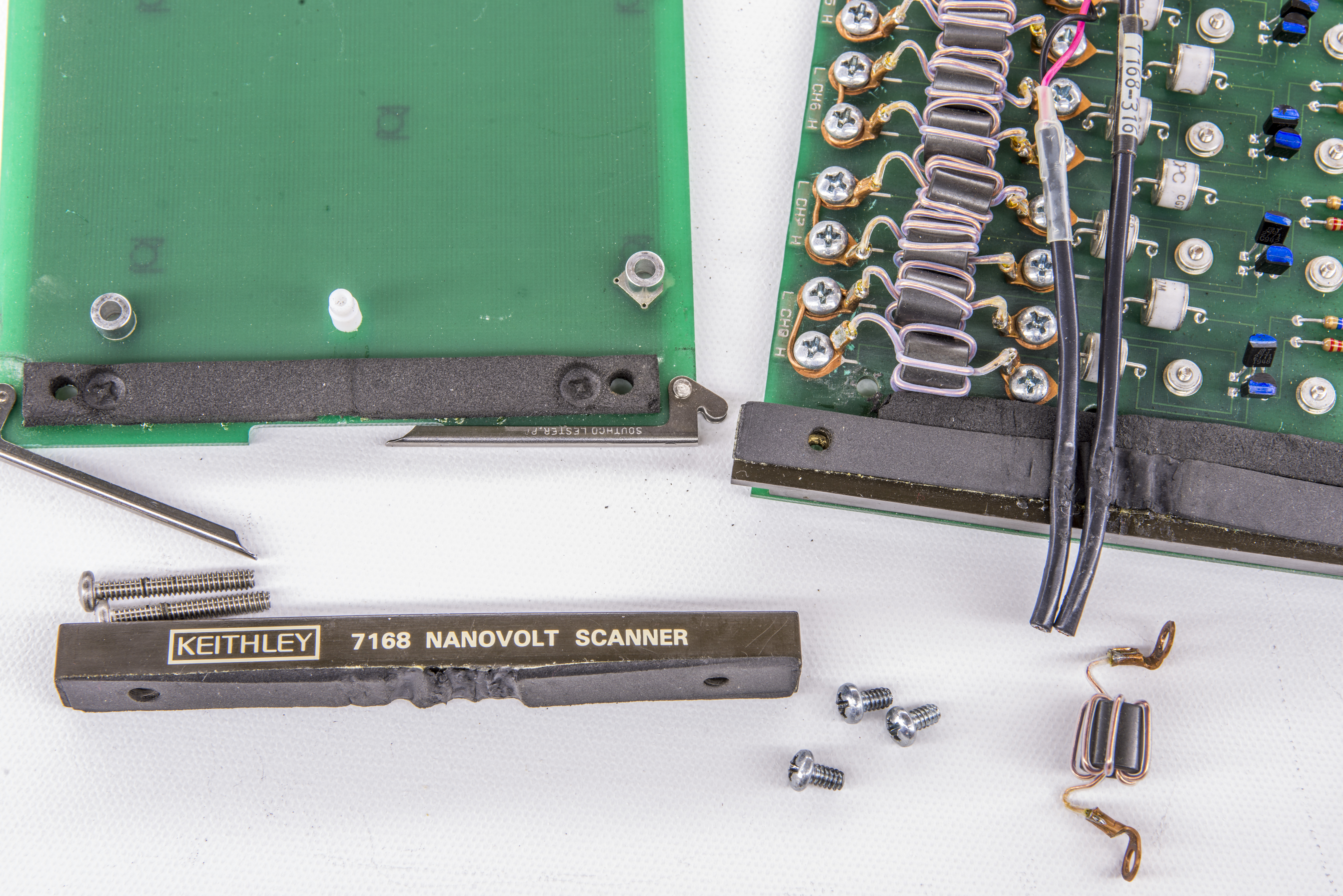
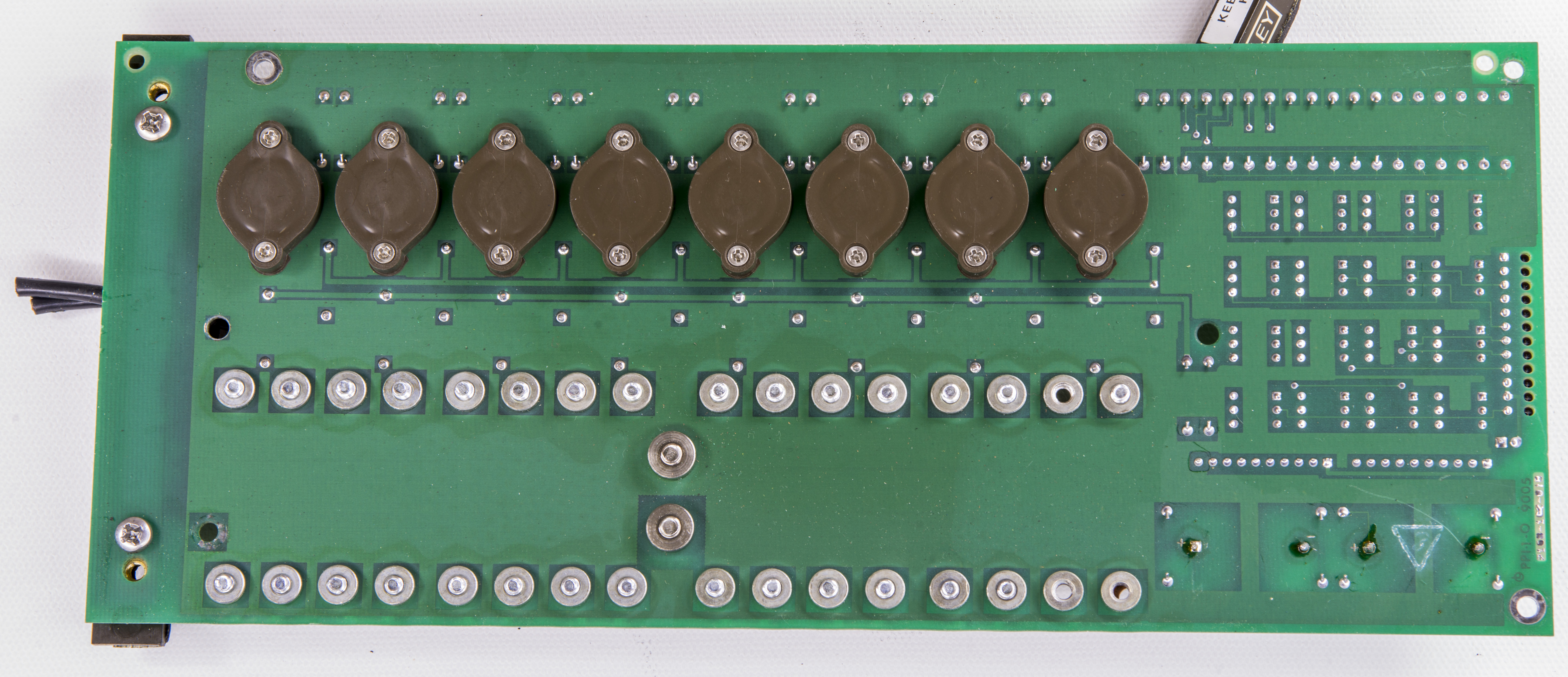
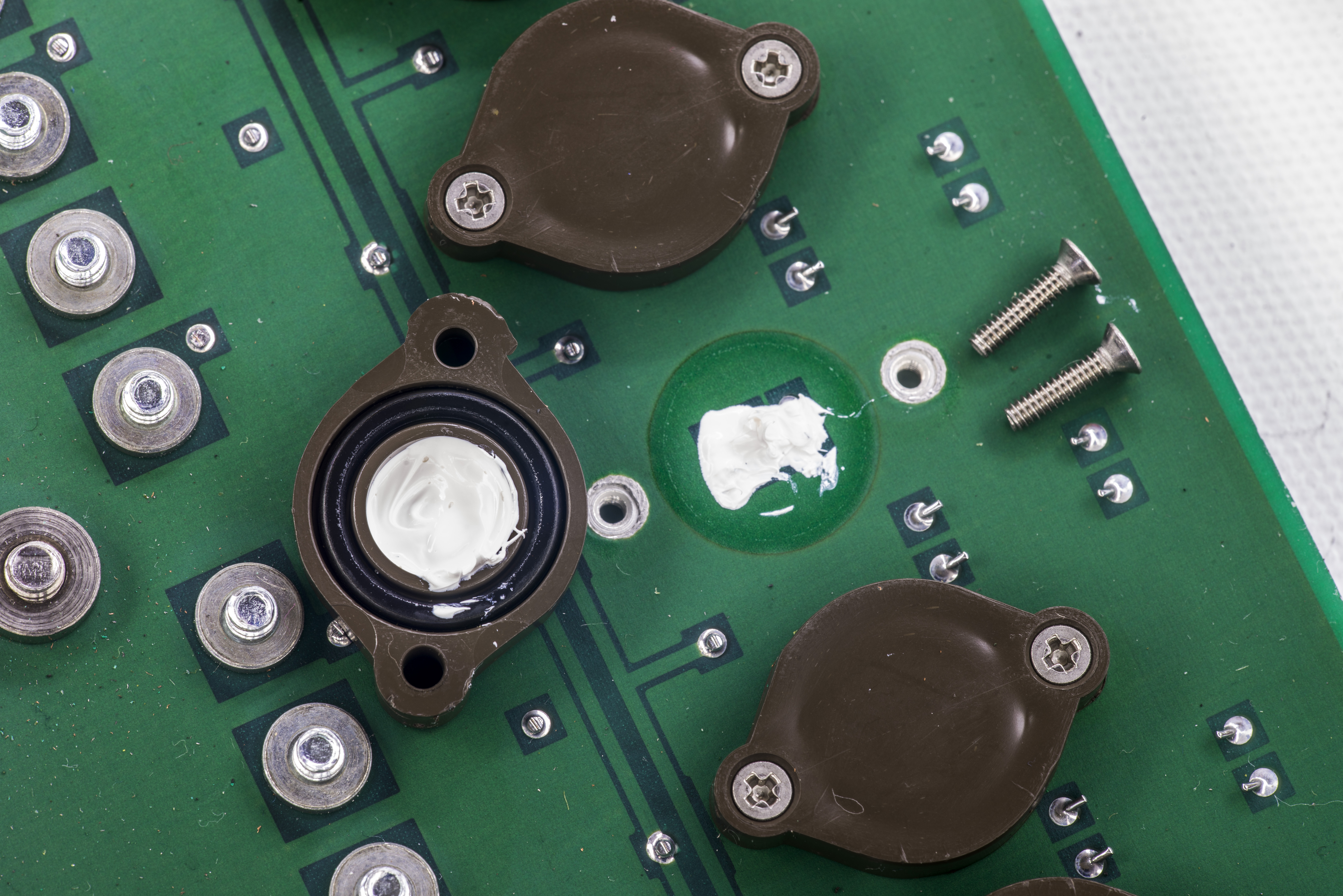
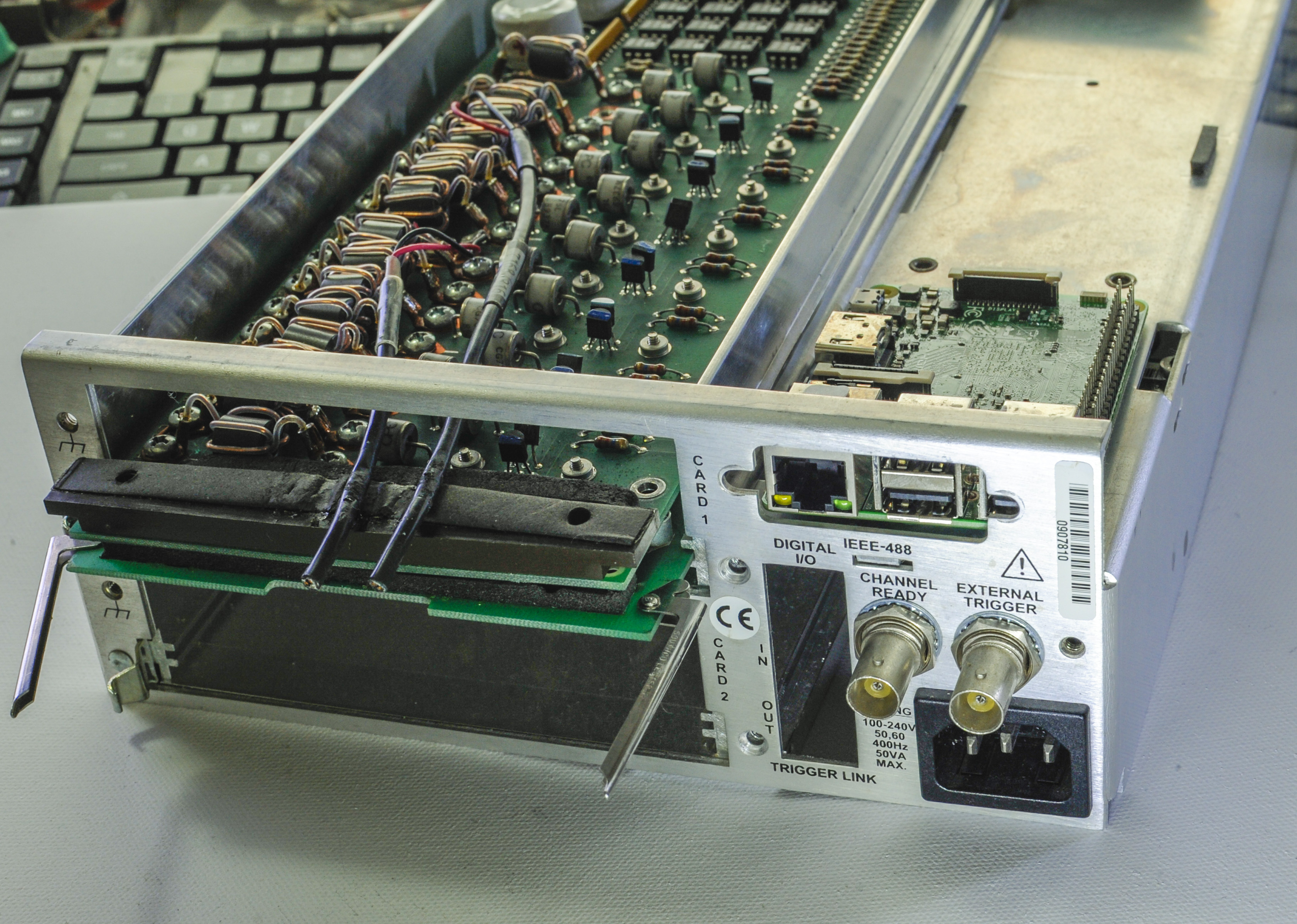
Teardown and construction review

JFET switching help to avoid relay self-heating offset errors. It also allow for channel resistance to be repeatable and consistant over long time, which often important for metrology applications.

FETs used in Keithley 7168 can close channel to output with series resistance around 10 Ω. Usually it’s not a problem, as in typical nV-scanner application output connected to high-impedance sensitive voltmeter. With typical impedance >1 GΩ resulting currents thru JFETs are in picoampere levels, and temperature increase of switch junction is essentially zero. However if low-impedance device connected on the output (such as ADC front-end) large mA-currents could flow thru scanner. It’s recommended to let channel stabilize for few hours to reach required thermal equilibrium for best accuracy.

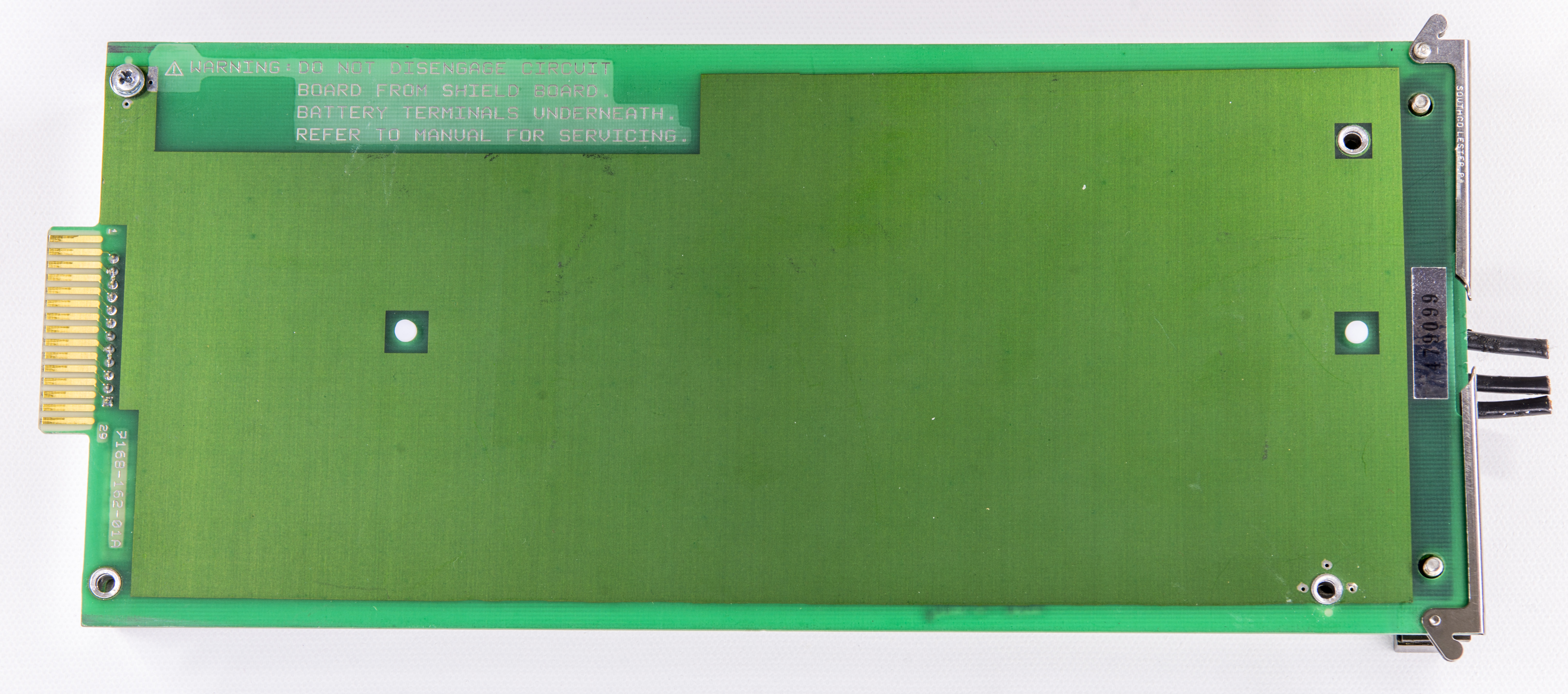
Due to isolated interface Model 7168 scanner card have separate onboard power source, which is two 15V lithium batteries. These batteries provide required bias voltage for JFET switches. Be careful not to short battery exposed pins when removing shield and making connections.
Battery BT1 supply bias for HI side of JFET switches. Second BT2 supply bias for LO side channels. Use of two separate isolated batteries allow to maintain high isolation between both high and low signal path on each channel.

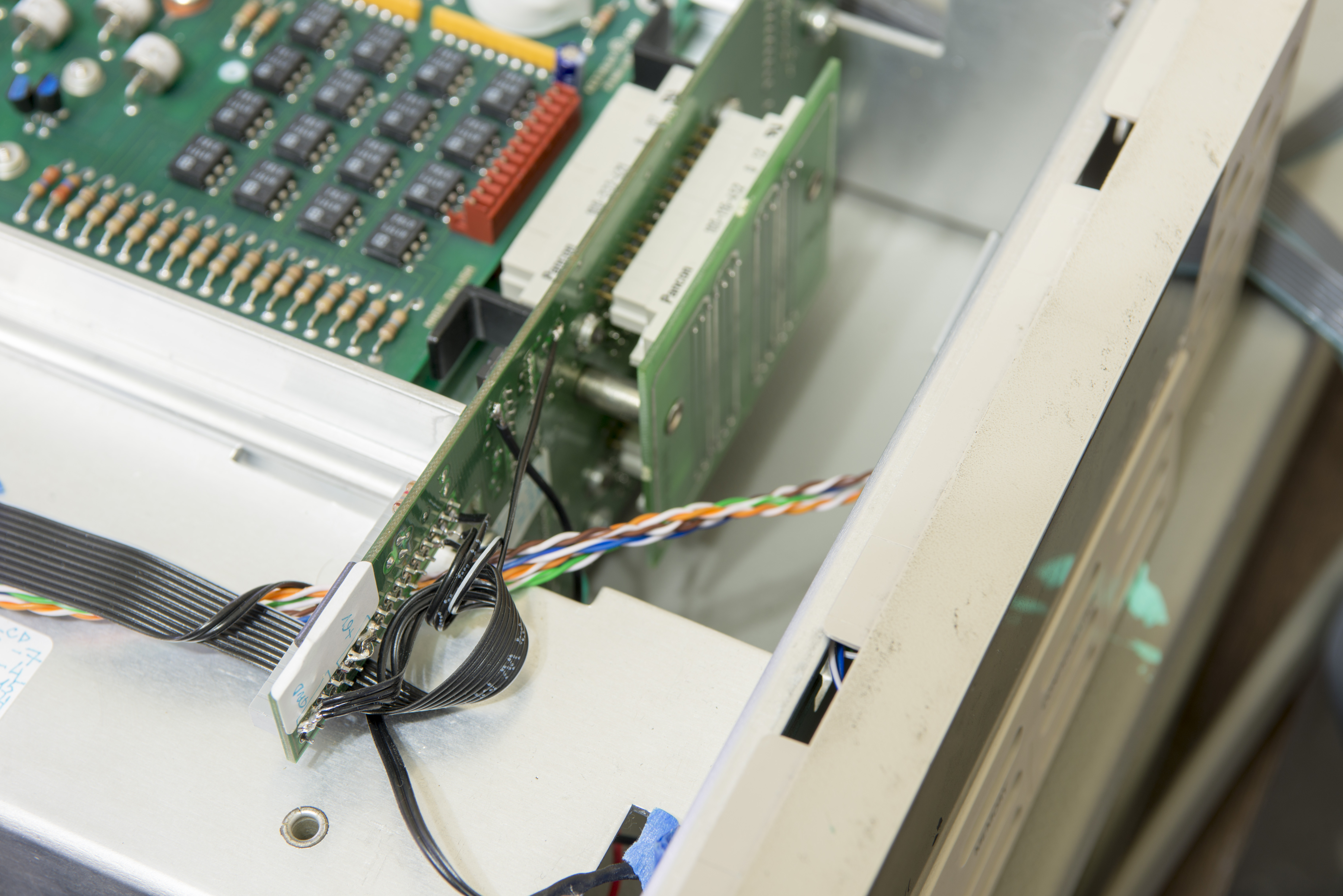
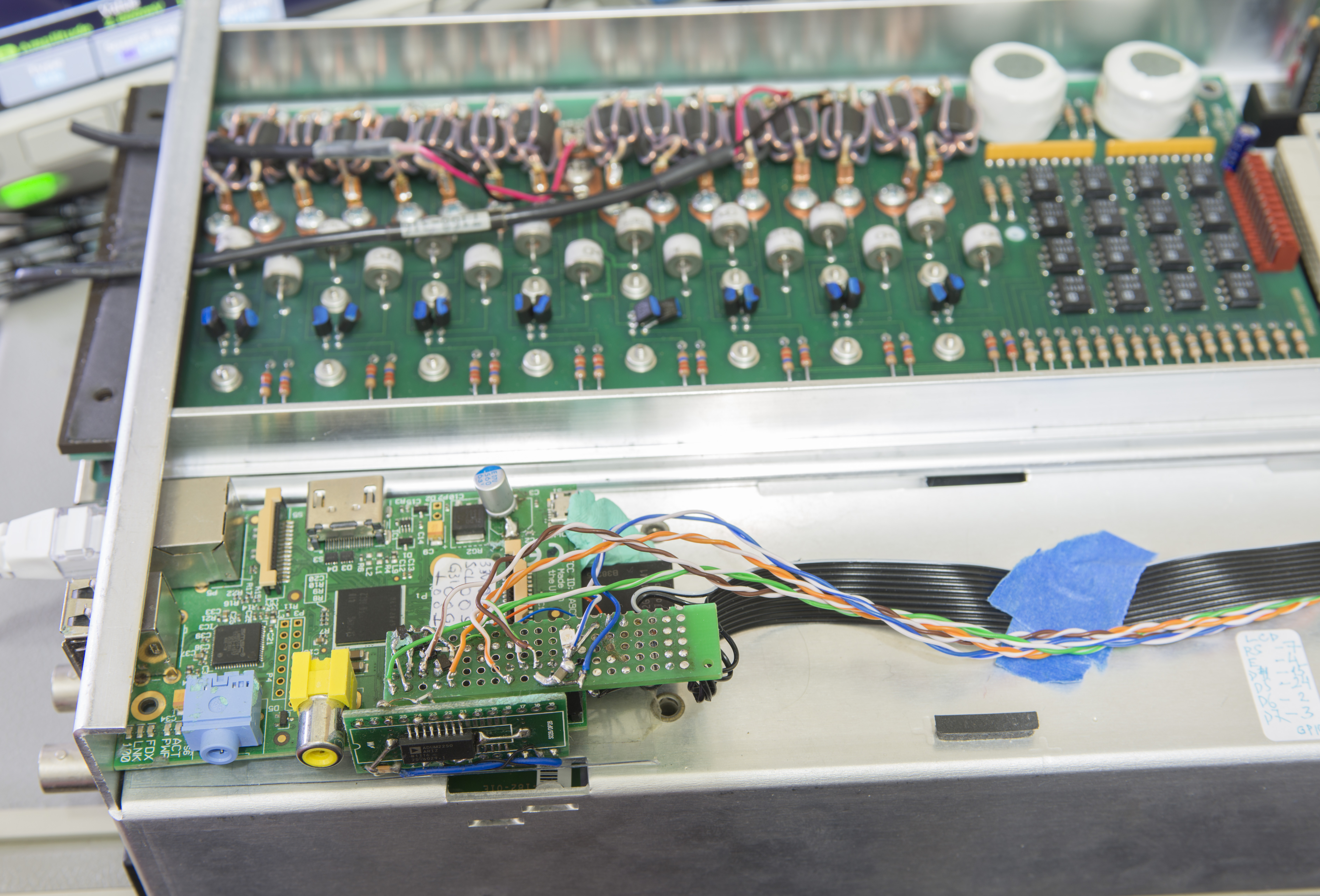
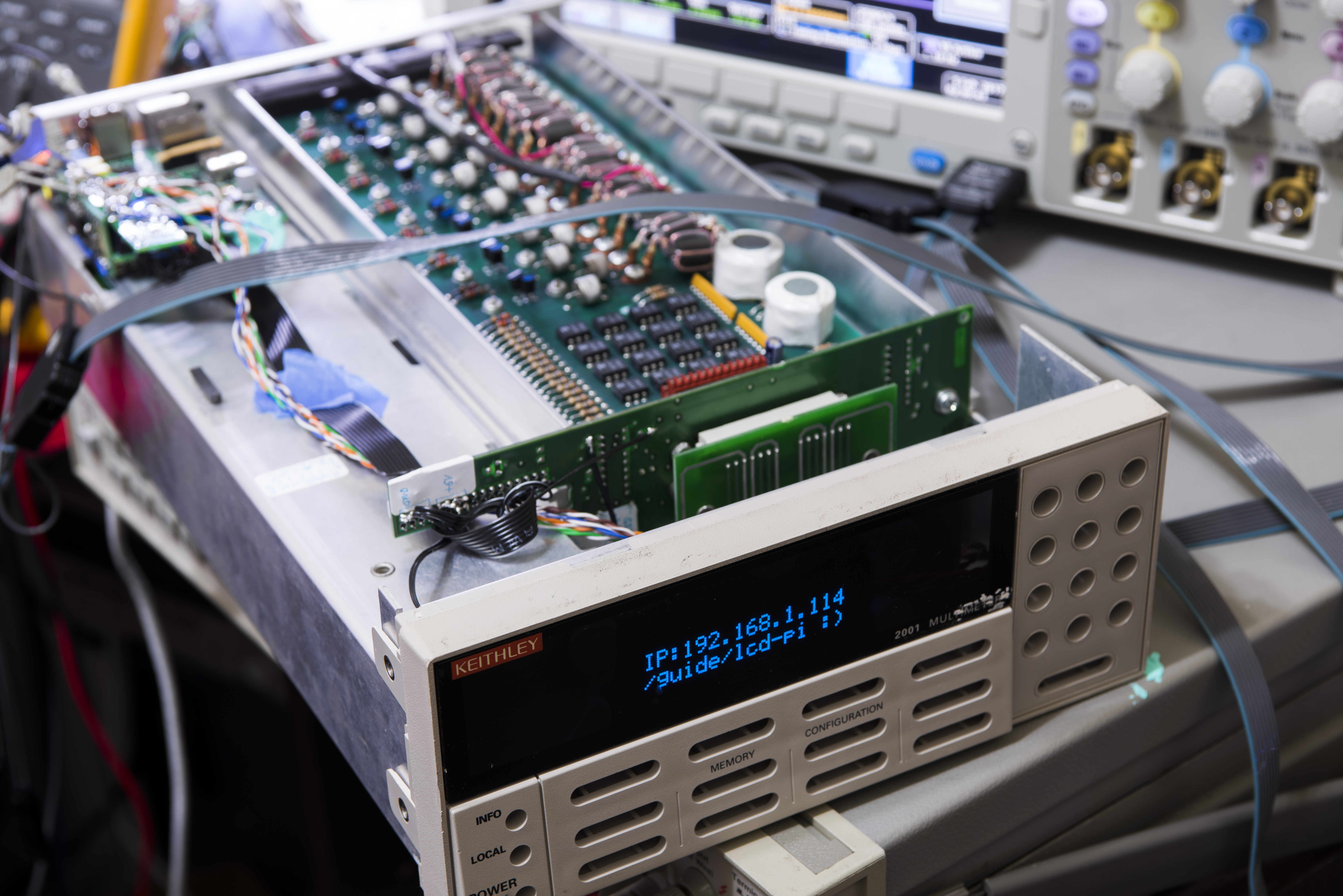
Raspberry Pi software to control Keithley 7168
To control scanner card actual Keithley 7001 backplane board 7001-176 was used. This board have UCN5841A serial 8-bit latched drivers, so with simple SPI interface and Raspberry Pi we can control. Keithley 7001 I have was salvaged for parts (front-panel VFD, parts from digital board) but chassis and power supply are still good and useful for this project. Raspberry Pi brings second life to these parts, and provide modern LAN interface for easy programming and control.
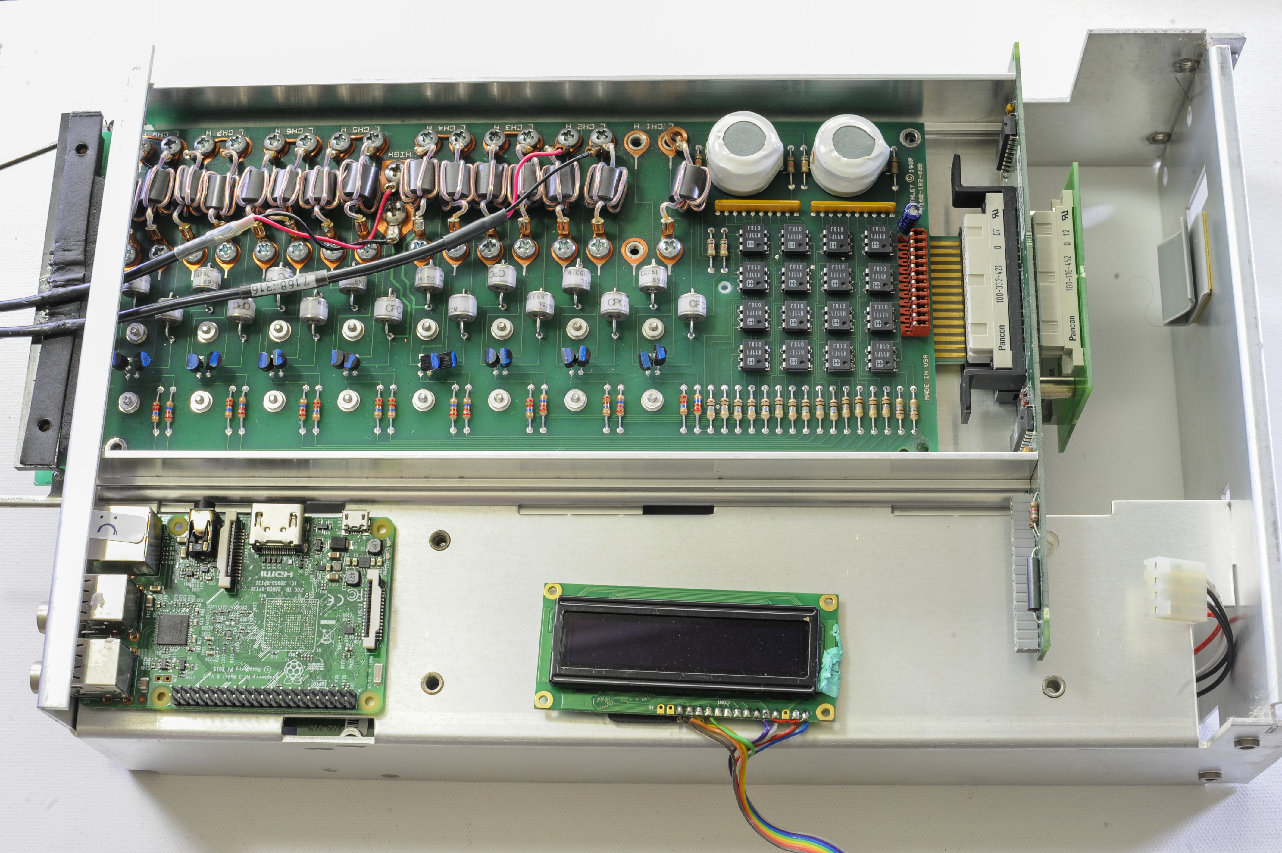
Actual Keithley 7168 signal mapping
| Channel | Interface pin | Inner board Connector | Mode |
|---|---|---|---|
| CH8 | Edge pin 23 | J2 pin 1 | Closed when low |
| CH7 | Edge pin 21 | J2 pin 2 | Closed when low |
| CH6 | Edge pin 19 | J2 pin 3 | Closed when low |
| +6.0 VDC Power | Edge pin 17,18 | J2 pin 4,5 | Power |
| CH4 | Edge pin 13 | J2 pin 6 | Closed when low |
| CH5 | Edge pin 11 | J2 pin 7 | Closed when low |
| CH2 | Edge pin 9 | J2 pin 8 | Closed when low |
| CH3 | Edge pin 7 | J2 pin 9 | Closed when low |
| Ground return | Edge pin 5,6 | J2 pin 10,11 | Ground |
| CH1 | Edge pin 3 | J2 pin 12 | Closed when low |
And installing card into top bay brings this map for SPI code.
| Register.pin Bit | Bit offset | Card J2000A/K7168 signal |
|---|---|---|
| U700.18 Bit Q1 LSB | 1 << 0 | Channel 1 |
| U700.17 Bit Q2 LSB | 1 << 1 | Channel 2 |
| U700.16 Bit Q3 LSB | 1 << 2 | Channel 3 |
| U700.15 Bit Q4 LSB | 1 << 3 | Channel 4 |
| U700.14 Bit Q5 LSB | 1 << 4 | Channel 5 |
| U700.13 Bit Q6 LSB | 1 << 5 | Channel 6 |
| U700.12 Bit Q7 LSB | 1 << 6 | Channel 7 |
| U700.11 Bit Q8 LSB | 1 << 7 | Channel 8 |
| U700.18 Bit Q1 MSB | 1 << 8 | Not used |
| U702.17 Bit Q2 MSB | 1 << 9 | Not used |
| U702.16 Bit Q3 MSB | 1 << 10 | Not used |
| U702.15 Bit Q4 MSB | 1 << 11 | Not used |
| U702.14 Bit Q5 MSB | 1 << 12 | Not used |
| U702.13 Bit Q6 MSB | 1 << 13 | Not used |
| U702.12 Bit Q7 MSB | 1 << 14 | Not used |
| U702.11 Bit Q8 MSB | 1 << 15 | Not used |
DIY scanner controller


Leakage test
Voltage offset test
Results and summary
Projects like this are born from passion and a desire to share how things work. Education is the foundation of a healthy society - especially important in today's volatile world. xDevs began as a personal project notepad in Kherson, Ukraine back in 2008 and has grown with support of passionate readers just like you. There are no (and never will be) any ads, sponsors or shareholders behind xDevs.com, just a commitment to inspire and help learning. If you are in a position to help others like us, please consider supporting xDevs.com’s home-country Ukraine in its defense of freedom to speak, freedom to live in peace and freedom to choose their way. You can use official site to support Ukraine – United24 or Help99. Every cent counts.
Modified: Aug. 6, 2018, 8:31 p.m.