Contents
- Intro
- EVGA EPOWER V theory and design
- EVGA EPOWER History tour
- Feature overview
- Usage methodology
- STEP 1 – Prepare workbench area and gather all required tools
- STEP 2 – Remove onboard VRM inductors
- STEP 3 – Make sure PWR_GOOD is activated to allow GPU operation
- STEP 4 – Expose copper plane for ground and power on target device
- STEP 5 – Solder the EPOWER down to the card
- STEP 6 – Final check and first power on
- EPOWER output voltage control
- Firmware update procedure and available firmwares
- Software toolkit
- Conclusion and feedback
Intro
Refreshed EVGA EPOWER V The Untouchables stand-alone power board returns. It’s been quite some time since release of the previous Gen 4 model in 2013. EVGA EPOWER module is handy and versatile tool to provide more juice to various graphics adapters, especially physically and power constrained reference designs from NVIDIA and AMD. This is crucial device for extreme overclocking and benchmarking with liquid nitrogen cooling.
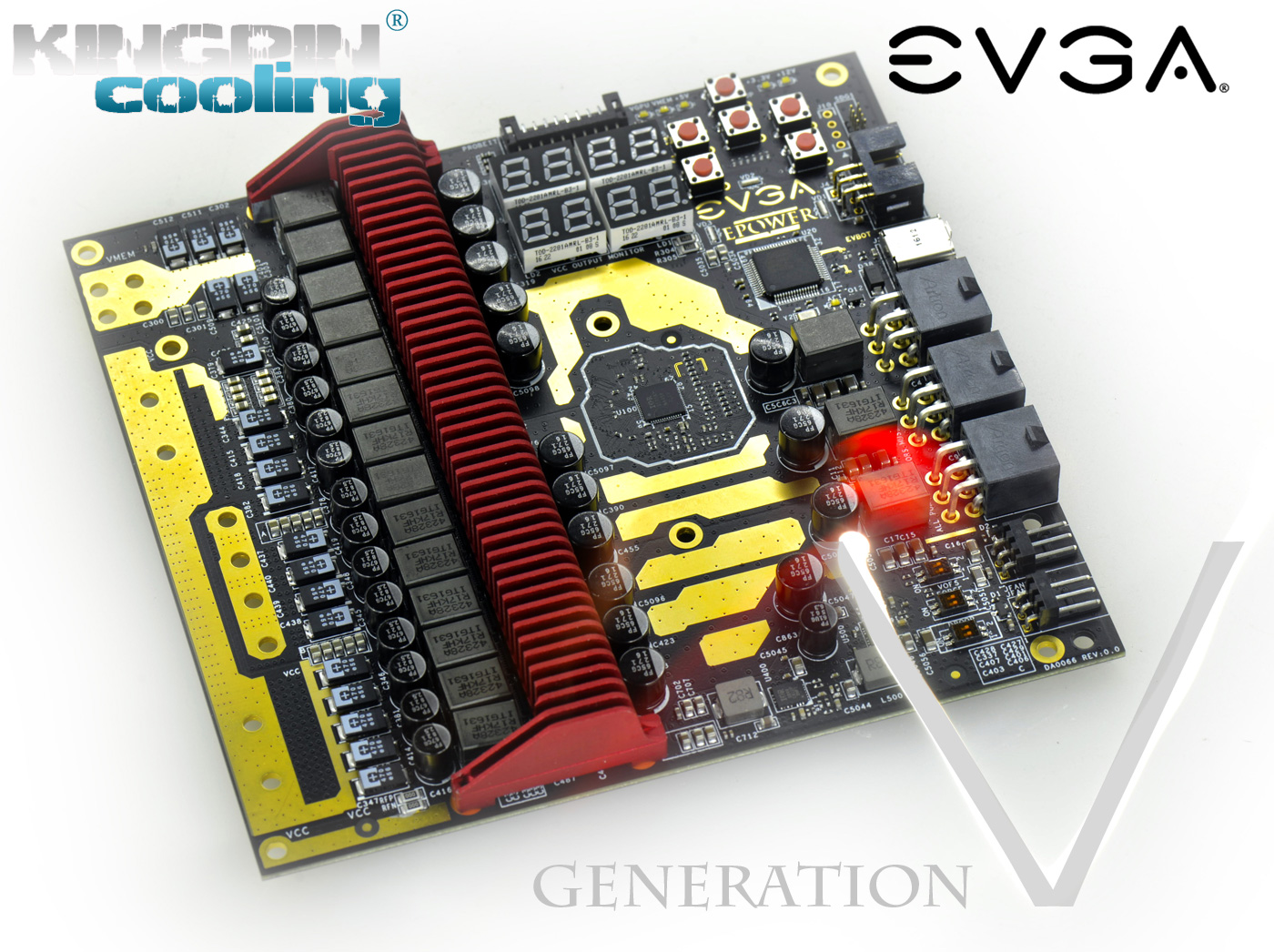
Image 1: EVGA EPOWER V introduction
This is fifth version of the EPOWER project, released in retail, targeted directly to extreme overclockers and hardcore enthusiasts. For this reason, it has the label “Generation V”. Previous EPOWER Gen 4 Classified with blood-red PCB resemble EVGA GeForce GTX 680 Classified power solution. New EPOWER V leverage more efficient and higher power VRM from EVGA GeForce GTX 980Ti K|NGP|N Edition card. This VRM iteration was further tuned up with latest IR3575/IR3579 Infineon PowIRStages that have improved thermal and electrical performance.
EPOWER V has synchronous buck DC-DC converter with no less than 12+2 phase layout. Such converter use input +12 VDC voltage from standard PC PSU to provide stable and regulated 0.6 – 2.0V output voltage, at maximum loading over 600 Amp. Additional 2 phase DC-DC regulator used for second voltage rail channel, with individual control and current capability up to 90 A. Second channel can be used for memory power on graphics card or PEX/PLL power.
Since different VGA cards may require different output voltages, both settings are adjustable in real-time. In this article we will cover common use scenarios and possible ways to adjust voltage, protection limits and other available tweaking knobs.
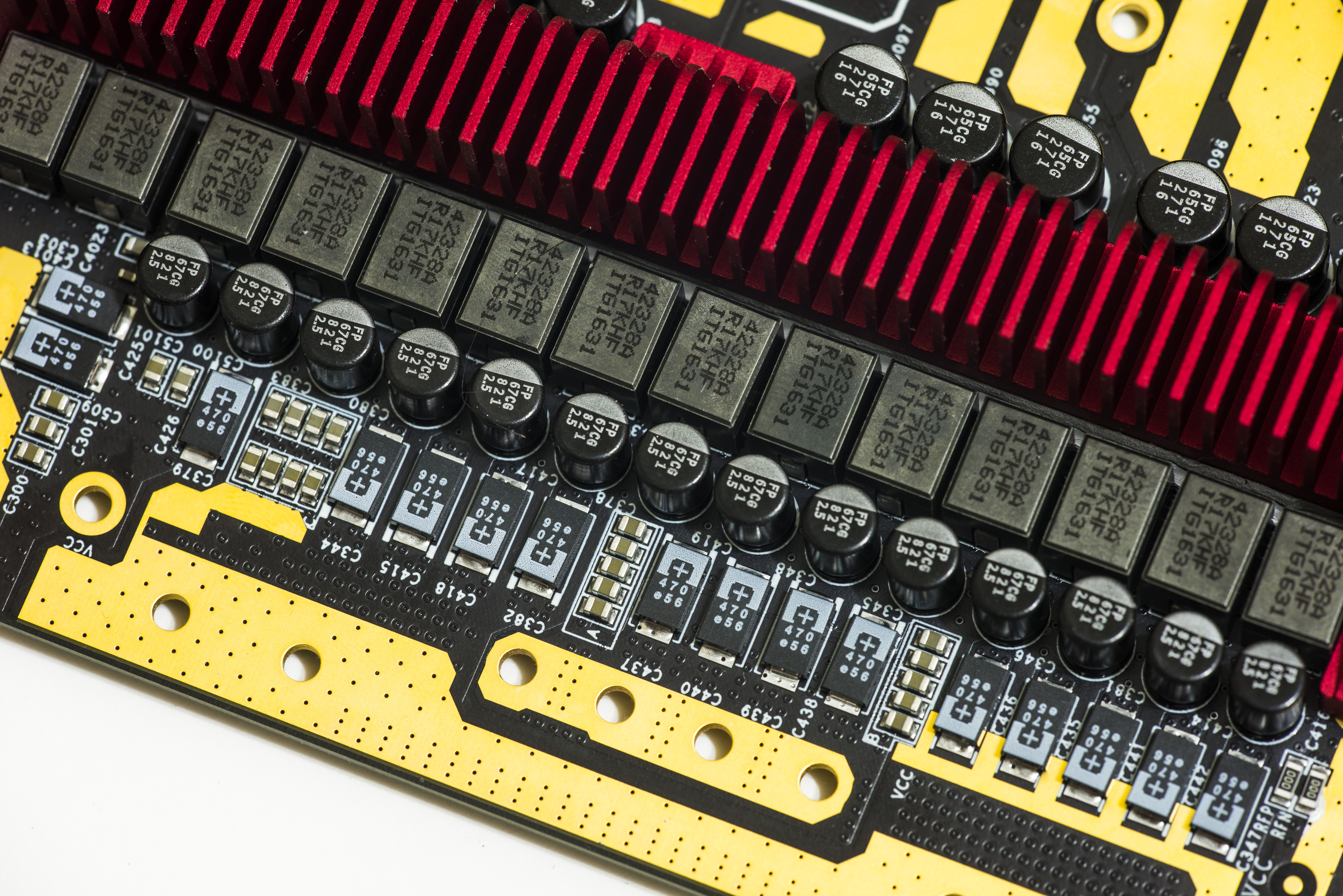
Image 2: Output power plane, filtering capacitor banks
Following previous versions of EVGA EPOWER boards, connection to target graphic card is done by direct soldering with heavy gauge copper wire or solid copper plates. With very high currents and low voltages, it is essential to have minimal resistance of the interconnect between the VGA card and EPOWER. Wide and short connection is the main rule here.
Due to complexity of use, EPOWER V is covered only by special DOA type warranty. Meaning that every single EVGA EPOWER V board is tested before shipment and can be replaced only if it’s not working on arrival, out of the box, with only ATX PSU attached to it. If you already modified your VGA, soldered EPOWER down, there will be no replacements possible. Be sure to check EPOWER correct output prior to connecting it with VGA card.
Disclaimer
Before we dig deep into details, please review usage agreement. If these risks not accepted, do not attempt to use external VRM board on your system.
Redistribution and use of materials in this article or any files referenced in it, in source and binary forms, with or without modification, are permitted provided that the following conditions are met:
- Redistribution of article must retain the above copyright notice, this list of conditions, link to this page (https://xdevs.com/guide/epower_v/) and the following disclaimer.
- Redistribution of files in binary form must reproduce the above copyright notice, this list of conditions, link to this page (https://xdevs.com/guide/epower_v/), and the following disclaimer in the documentation and/or other materials provided with the distribution, for example Readme file.
All information posted here is hosted just for education purposes and provided AS IS. In no event shall the author, this site, or any other party, including EVGA be liable for any special, direct, indirect, or consequential damages or any damages whatsoever resulting from loss of use, data or profits, whether in an action of contract, negligence or other tortuous action, arising out of or in connection with the use or performance of information published here.
This product is intended for use by advanced users with good understanding of computer parts function, decent soldering skills and experience in extreme overclocking. There is no benefit to use such device for everyday gaming, as native VRM on the graphic card is a good match for everyday use cases.
If you do not agree with risks involved, do not perform the any modifications to any of your hardware. If you think there is a mistake in this OC Guide, please contact us thru comment section on this page, or at Kingpincooling.com forum thread.
EVGA EPOWER V theory and design
Before we start any soldering and testing, please take a brief tour into typical VRM design. VRM is an electronic device, usually in form of circuitry on PCB which consist of DC-DC converter and controller, which provides the appropriate power supply voltage to the load. This is achieved by operation of the switching regulator, which convert higher input voltage (such as +12.0 VDC from ATX PSU PCIe power cable) to a much smaller voltage level required by the load specifications. Since the total power is the same, lower voltage allow to source much higher currents, used by all those billions of transistors inside the CPU/GPU chip.
Load here and further in article meaning target device which receive the power, such as central processor on motherboard or GPU on the graphics card. From power supply point of view, it doesn’t matter what is used as load, it could be even piece of heating wire, concept remain the same. Common and important thing is that load sink provided current, depending on its own dynamic and static internal resistance and power demands. Task of the VRM is to provide that current and regulate output voltage, maintaining stability under any dynamic conditions.
Why not to supply already regulated lower voltage from the PSU directly? Answer to that question is resistance of interconnects and power loss on wires. Modern GPU can easily sink over 200 A of current, which would need very bulky and heavy gauge wires. Since GPU also have strict voltage regulation demands (usually 5% or better) there is no way to provide that much of current with any reasonably sized (and priced) wires or connectors to lengths over more than few centimeters (inches). That’s why any typical motherboard or graphics card has these switching DC-DC converters onboard, right next to CPU/GPU. Sometimes VRM are installed as daughter boards with special dedicated high-power connector (common to see such VRM modules in rack servers, where every inch of space is vital).
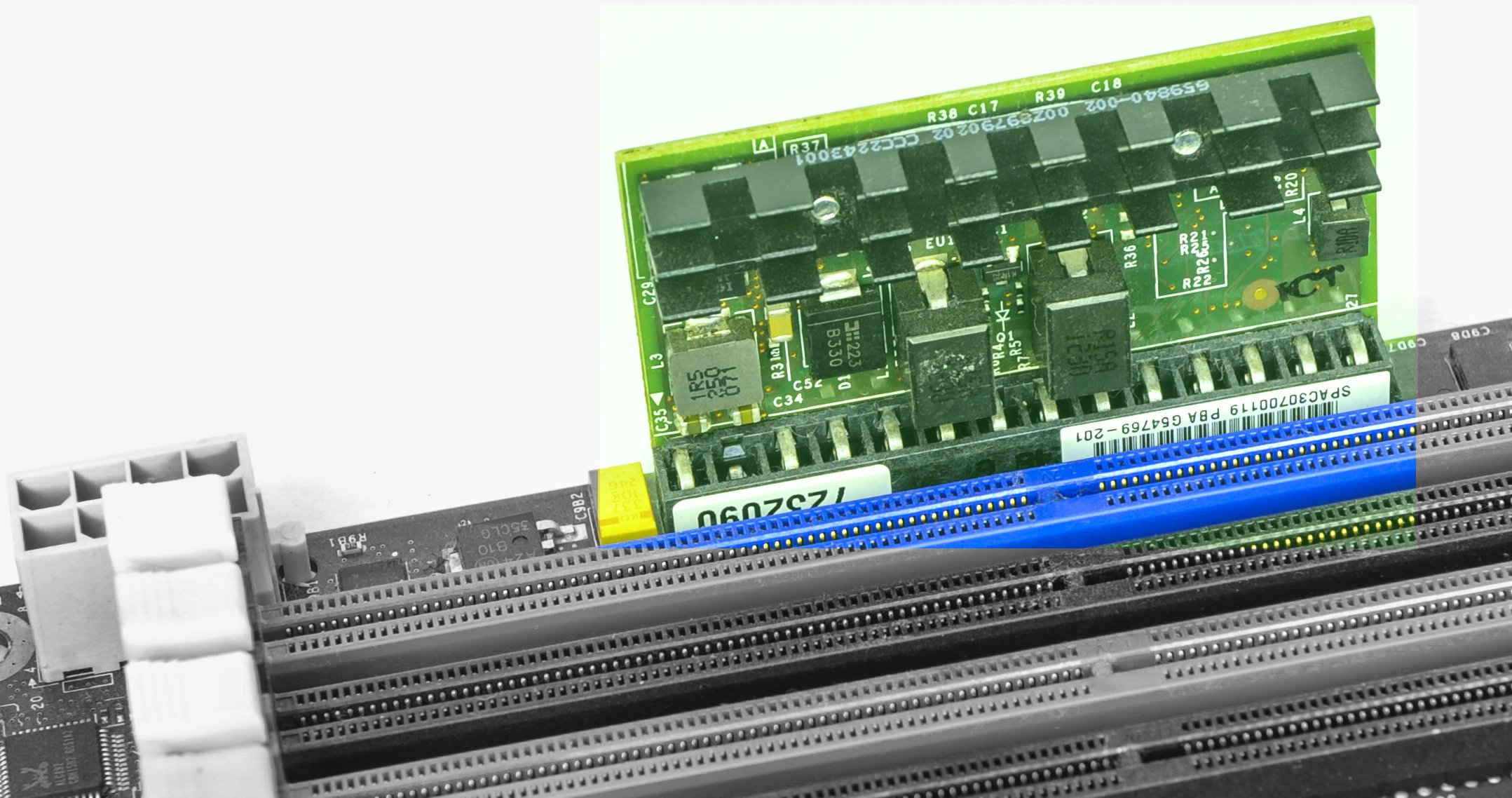
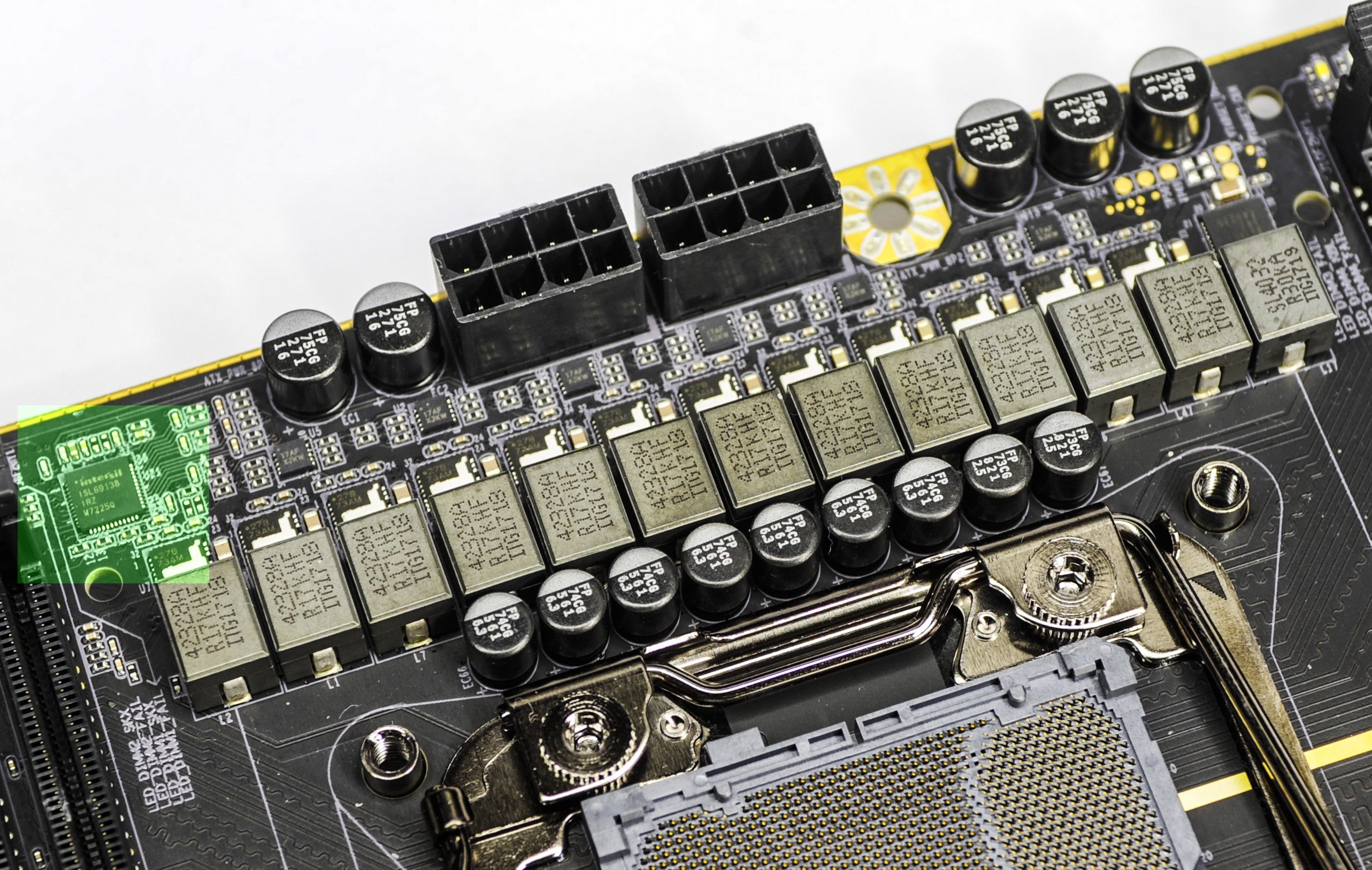
Image 3: 2φ DC-DC regulator on module (left), 12φ DC-DC regulator and controller on MB for CPU (right)
It is easy to recognize power regulator circuit by proximity with high-current ferrite inductors and banks of capacitors. Multi-phase regulators have all phases grouped together, to maintain good current and thermal balance across phases. Proper spacing to rest of the sensitive circuitry on the PCBA (memory, I/O interfaces or onboard controllers) is implemented due to large amounts electrical noise generated by switching components in VRM.
Some simple voltage regulators provide only fixed voltage level at the output, but most of them have voltage adjustment functionality, controlled by the load or onboard logic, using some form of standard interface. Such interface can be simple parallel VID signals or simple analog feedback circuitry. Multi-phase VRMs that designed for modern CPU or GPU power also can use dedicated digital bus, such as I2C/SMBus/PMBus or SVID/PWMVID to communicate operation status, reporting and control data with onboard power managment logic.
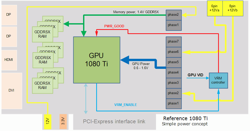
Image 4: Simplified VGA Power concept block diagram
Image 4 show typical high-level VRM map of GeForce GTX 1080 Ti reference graphics card. Ignoring number of phases and type of connectors, every VGA card is build this way. Two important logic signals, VRM_ENABLE and PWR_GOOD are discussed in next sections.
VRM controller also needs its own power supply voltage to operate. This is usually system auxiliary low-voltage rail, such as +3.3 VDC from the PCI-express edge connector. +3.3V voltage is used for digital domain of the VRM, like PWM controller IC, signal drivers, onboard clock generation parts, control circuits and various other onboard logic. +3.3 VDC often used by onboard display controllers and I/O devices, SLI interface power, BIOS, hardware health monitors, I/O detection logic and such. That’s why PCI-Express CEM standard for AIC always have +3VDC and +12VDC power inputs at PCI-Express slot edge connector. +12V used for lower power DC-DC and +12V from separate 6/8-pin power cable from PSU. Latest generation videocards may have also +1.8V, regulated by additional small VRM to reduce idle power and provide better efficiency under low load conditions.
In this article we will study typical example of the VRM circuitry, used in 1080 Ti and will show how to use, control and override these converters with EPOWER help. EPOWER V is a great example to learn all related knowledge. This is especially important for overclocking and performance testing, as voltage margining often is the key for higher frequencies, once thermal limitations are removed (meaning use of LN2(Liquid Nitrogen) which boils at -196 °C).
Many controllers allow shutdown control and power good status reporting. For that dedicated GPIO signal line and pins are used. Such signals described as “ON/OFF” or “VR_Enable” or simply “Enable” signal and power good status reported via “VR_RDY” or “PWR_OK” signal/pin in datasheets.
Enable signal in VRM operation
Purpose of VRM_ENABLE signal is to provide ability to turn on (Enable) or off (Disable) main VRM by our GPU or other smart monitoring circuitry that may be present onboard. This signal has input direction, feeding signal into the VRM controller. Let’s take simple example in term of generic 1080 Ti videocard depicted on Image 4 above. 1080 Ti GPU used on this card have special GPIO pin hooked to VRM_ENABLE signal on PWM. During startup, I/O block of 1080 Ti chip pulls this signal high, thus giving command for VRM to start operation and power-up. VRM begin to operate at nominal level, which is around 1 VDC output. Once output reached stable regulated level, VRM controller activates PWR_GOOD signal, which is often tied to GPU’s RESET input, and let GPU start initialization and boot. If for some reason PWR_GOOD is not active (stay low level, 0V) then GPU will be kept in RESET condition and will not boot.
Why we need such arrangement, and not let VRM to start and run on its own? This “ENABLE” handshaking between GPU and power regulator allow to implement protection mechanism, for example overheating protection. Assume that user forgot to connect fans on cooler, resulting critical GPU overheat while VRM continue to source power into the chip. VRM still feeding GPU with nominal voltage, as it can’t know anything about GPU temperature. GPU will cook itself to death short due to thermal runaway if no action taken quick. Silicon die, like GPU, will consume more power as the temperature rise, and shortly after temperatures over +120°C consumed power and temperature will jump exponentially till the physical internal damage occur.
However, during overheat event GPU chip can monitor its internal temperature sensor and forcefully pull down VR_ENABLE pin to low (0 V). As result of this VRM now will immediately shut down output voltage, as result preventing possible damage to graphics card GPU. Do not confuse this with some other software-controlled shutdowns or protection triggers, such as OCP or OVP trip, which are soft failure modes and often internal to VRM. Protection trips are detected by VRM controller internally, and usually are not related to external logic. All these protection events can also be reported by reading the PWR_GOOD signal.
VR_ENABLE can have additional control from simple detector logic circuitry, build with small NPN or NFET transistors to always enable VRM if input power voltage +12V or +3.3V rail voltage from PCI-Express slot is present. This is why if you don’t have +3.3V/+12V power on PCIe slot VRM will be permanently disabled no matter which voltage we give to PCIe 6-pin power connectors.
Power good signal from VRM
Now few words about VR_RDY (Voltage regulator Ready) or how it is often also called, PWR_GOOD (Power Good) signal. In a way it has reversed meaning of VRM_ENABLE. This signal is output direction, from VRM controller into the GPU/control logic. When this signal is active high (+3.3 V), VRM is reporting normal operation, with stable and controlled output voltage, at rated settings, currents and temperatures. This is often used in high-end cards to monitor normal operation state of the VRM to detect faults and assert shutdown before critical failures progress further. For example, if MOSFET in the power stage phase blows up, VRM can quickly detect that phase current levels reach critical limits and report immediate failure to system, by dropping PWR_GOOD signal to low state. Similar method is used in usual ATX PSUs, by signal Power Good in 24-pin power connector.
Now let’s take a look on same block diagram, but with GPU power coming from our external EVGA EPOWER V module.
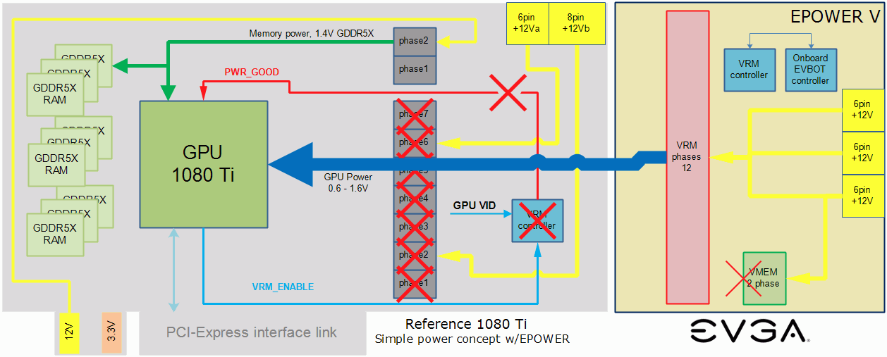
Image 5: Simplified VGA Power concept block diagram with EPOWER V
Standalone power supply module, such as EVGA EPOWER V is designed to replace onboard VCORE regulator to increase maximum power delivery capacity without voltage limitations. This is important for extreme overclocking use, as onboard DC-DC power converters on reference design are often not adequate for high voltage/high loading Extreme OC scenario. Often onboard regulators also lack of adjustment range, so you may be limited to lower voltage, than actual GPU can run before having thermal/stability issues. Image 5 shows same GTX 1080 Ti reference card block diagram, but it can be any other card, like GTX 980 or 8600 GTS, concept is the same.
While isolated supply module gives us freedom and voltage adjustment flexibility, it also does not come free. Difficulty of running card with EPOWER is due to inherent lack of sync between onboard VRM controller and EPOWER’s controller, as these are two separate controllers. So as result typical solution is to completely disable onboard VRM, isolate it from GPU and use EPOWER V regulator as a full replacement.
EVGA EPOWER History tour
Original first-generation EVGA EPOWER was cooked around year 2010 by legendary overclocker Peter “Shamino” Tan. That module was based on Volterra DC-DC chipset, one of the first 10-phase digitally controlled VRM solutions on the market. In 2013 Volterra Semiconductor was acquired by Maxim Integrated, and today is very rarely used on consumer PC hardware.
Same power solution reused in EVGA X58 SLI Classified 4-way SLI motherboard and EVGA GeForce GTX 285 Classified first 4-way SLI card on the market.
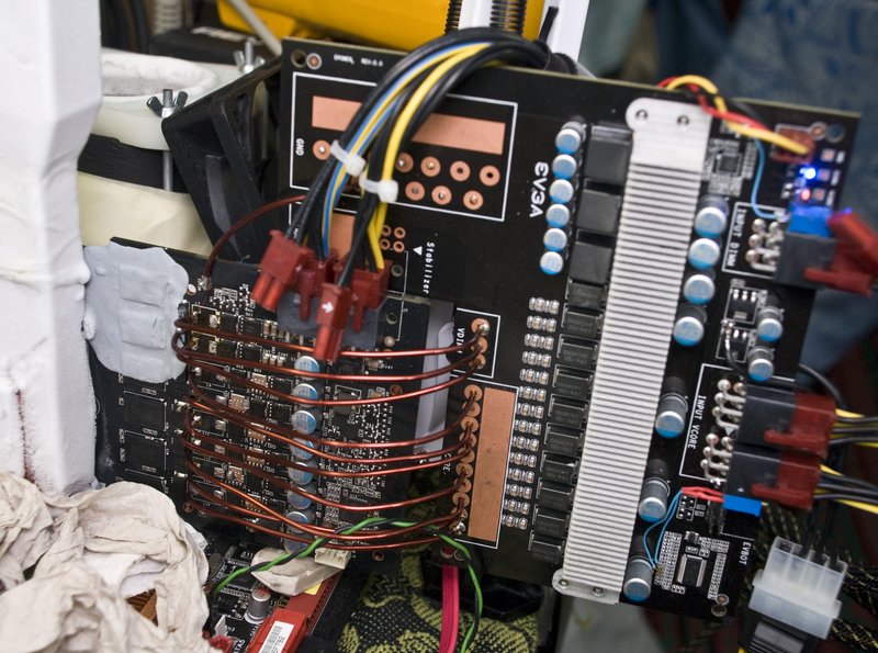
Image 6: EPOWER Gen 1, first prototype version. Never released in retail.
To get it more practical and user friendly, second generation use smaller PCB, but with same Volterra-based 10+3 phase power design. This version was sold in retail by EVGA in limited quantity of few hundred pieces, to provide overclockers handy tool for extreme overclocking sessions. Number of overclockers used it in their experiments and overclocking sessions:
EVGA EPOWER + GTX285, EVGA EPOWER + Radeon 6670
EVGA EPOWER discussion on overclock.net
EVGA EPOWER + GTX Titan
Image 7: EPOWER Gen 2, first unit to sell in retail, year 2012
Third generation in 2012 was even smaller size concept to feature just single output with just 8 phases, which is enough for chip like GTX 680. But before it got ready to see daylight, it became quickly obsolete with release of power monster GK200 GPU. As result this EPOWER was never released or sold in public. Only 10 pieces were made, on virgin green solder mask PCBA.
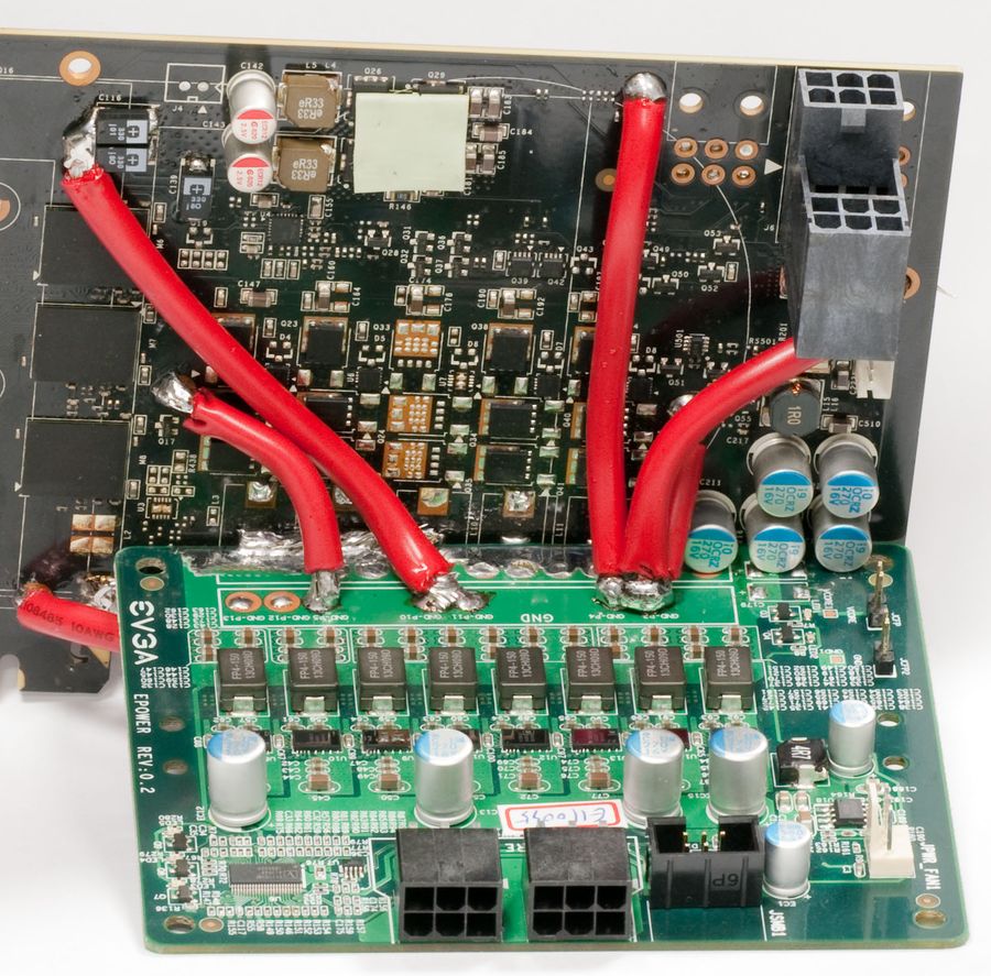
Image 8: EPOWER Gen 3, compact 8-phase VRM
Fourth generation from 2013 had a major change with design done from scratch to improve on all aspects. As result, end product had quite a feature list:
- Compact multi-layer PCBA for improved thermal performance
- DirectFET 14-phase design with maximum current 50A per phase
- CHIL digital controller with I2C interface for real-time control/monitoring
- Remote sense connector for precise output voltage regulation
- Onboard DIP switch to set Vboot voltage level
- Direct edge connection for lowest resistance possible between EPOWER and VGA
- Debug LEDs and ProbeIt header for easy monitoring
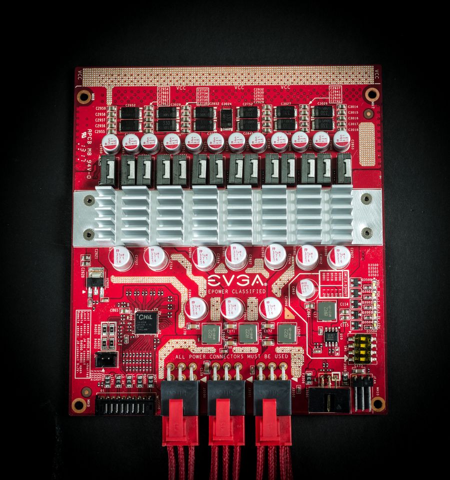
Image 9: EPOWER Gen 4, refreshed design for retail, sold during NV Kepler/Maxwell era
This EPOWER was in production and few hundred pieces were sold to extreme overclockers direct from online EVGA store. Gen 4 EPOWER is same proven VRM module later used in high-end graphic cards like EVGA GeForce GTX 780 Ti KINGPIN. Some folks even took their obsolete EVGA 680 Classified and turned into standalone EPOWER. If you prefer video tutorial, this one might be interesting.
And today new Gen V EPOWER further improve each of those points, with use of modern high-efficiency integrated power stages, adding second voltage channel for memory use, integrating EVBOT controller and using improved PCB layout.
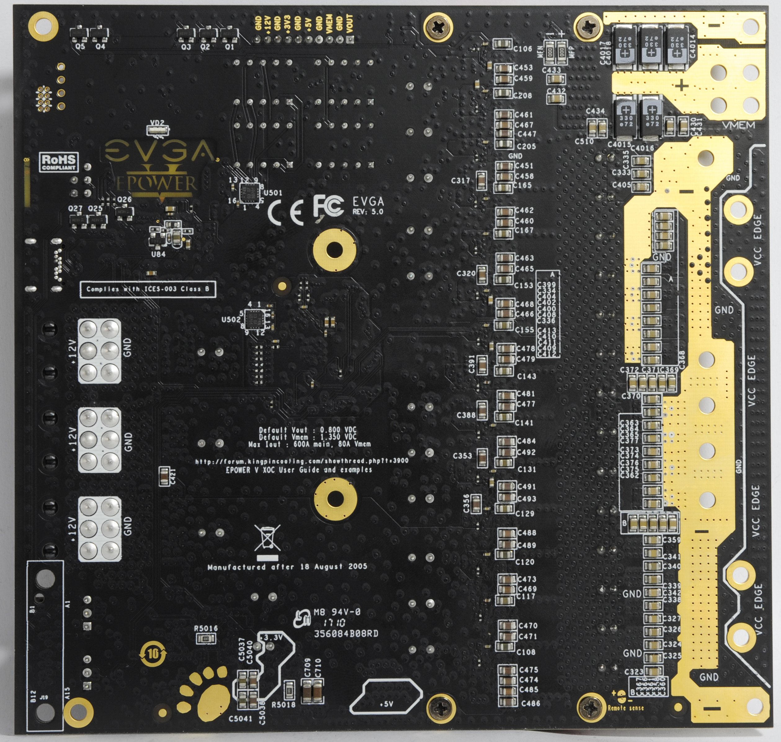
Image 10-11: Current EPOWER Gen 5 project. Top and bottom sides.
Same as Gen 4, board accepts input voltage from triple MiniFit Jr. 6-pin connectors, following typical PCIe VGA pin out. Input voltage range is +10.6 to +13.2 VDC, easy requirement for any high-end 1000+ Watt ATX PSU. For heavy loading, such as Titan Xp + EPOWER at least 1200 W single-rail PSU is recommended.
EPOWER V has two four-digit LED displays, which indicate current voltage on both channels. On key press setting value for output voltage is displayed. More on controls later in this guide.
| EPOWER Type | Gen 1 | Gen 2 | Gen 3 | Gen 4 | Gen 5 |
|---|---|---|---|---|---|
| Release year | 2010 | 2011 | 2012 | 2013 | 2017 |
| Power design | Volterra 10φ | Volterra 8φ | CHIL 14φ DirectFET | Infineon/IR 12φ IR3575/9 | |
| Secondary output | 3φ uPI VRM | None | Infineon/IR 2φ IR3575/9 | ||
| Max current, voltage | 600A + 50A, up to 2.1V | 400A, up to 1.8V | 600A, up to 2.0V | 620A + 90A , up to 2.0V | |
| Onboard control | None | None | 4-bit VID | Integrated EVBOT, keypad + LED display | |
| External control | EVBOT only | USB, EVBOT | |||
| Input power connectors | Triple 6-pin ATX VGA MiniFit.Jr | Dual 6-pin | Triple 6-pin ATX VGA MiniFit.Jr | ||
| Production model | No, ES only | Yes, retail | No, ES only | Yes, retail | Yes, retail |
| Power status monitor | 3 LED | 5 LED, ProbeIt | LED display, 7 LED, ProbeIt | ||
| Extra features | None | Remote sense | Remote sense, VCORE offset, protection off | ||
| Fan power for cooling | Single 3-pin fixed +12VDC header | Dual 3-pin fixed +12VDC header | |||
| Upgrade compatibility | None | Firmware available to user | |||
| PCB Design | 4-layer custom shape | 4-layer | 4-layer mini | 8-layer HP red | 8-layer HP black + gold plating |
| MSRP | N/A | $100 USD | N/A | $100 USD | $250 USD |
Table 1: Comparison of different EVGA EPOWER power modules
Latest generation is also more flexible now, in terms of use and hardware support. Firmware can be reprogrammed by user to allow special cases, when additional features or functions, such as protection, loadline tuning or monitoring are required. This may be crucial for overclocking modern cards, such as AMD Fury/Vega or NVIDIA Titan X/Xp. Additional firmwares will be made available thru this guide or it’s discussion thread at Kingpincooling.com forum.
EPOWER V using Infineon VRM controller, IR3595A. Key feature list:
- 8-phase single or 6+2 dual loop configurable PWM Controller. Here it’s used as 6+1 dual loop.
- 8-bit PVID, PWM VID or I2C set point control on loop 1
- Serial I2C set point control on optional loop 2
- Programmable Constant Current Protection
- Min/Max Telemetry registers and real-time monitoring via I2C (IIN, VIN, IOUT, VOUT, Temp)
- IR Adaptive Transient Algorithm (ATA) minimizes output bulk capacitors and system cost
- IR Efficiency Shaping Features including Variable Gate Drive and Dynamic Phase Control
- Protection: OVP, UVP, OC Warn, OCP, OT Warn, OTP
Loop in power terminology here is referred to output voltage channel, and EPOWER V implements both loops as detailed in table below:
| Loop | Output voltage | Output configuration | Max current |
|---|---|---|---|
| Loop 1 | 0.600 – 2.000 VDC | 12 phase IR3579M PowerStage | 600 Amp, 620A peak |
| Loop 2 | 0.600 – 2.200 VDC | 2 phase IR3579M PowerStage | 80 Amp, 90A peak |
Due to safety reasons, maximum output voltage is limited around 2.000V. Most modern VGA cards have capacitors on Vcore rated only up to 2.000V, and will max out overclocking at much less voltage, even under liquid nitrogen -196 °C cooling. Solid capacitors may have nasty explosions and fire if overvoltage happens, so voltage limits greatly reduce this risk.
EPOWER board can be a very handy tool for new GPU testing, as it can be used the moment we get the reference cards for overclocking. Based on those test results, not limited by power constrains of voltage limits, finalized custom designs like KINGPIN Edition and FTW3 emerge, which essentially have both EPOWER and GPU circuitry already integrated on the same PCB, without any mess and wires.
Also onboard controls are added, so no external EVBOT dongle required to get voltage readout of real-time voltages on both VCORE and VMEM rails. Output voltages can be also freely adjusted at any time by onboard keypad.
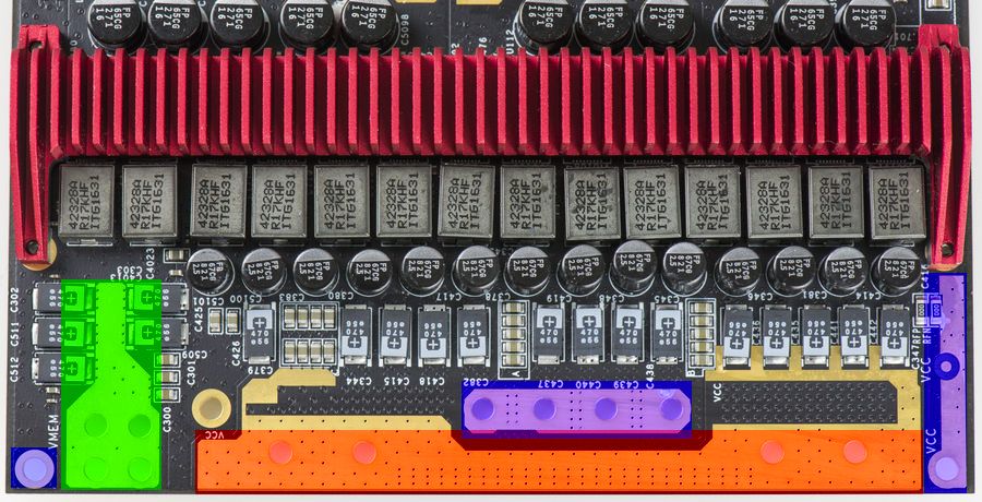
Image 12: Output power connection area. VMEM exposed plane (left, green), main VCORE (red, center), GND (blue)
Feature overview
Here’s quick fact sheet with main features list on this latest generation EVGA EPOWER V VRM.
Dual-channel powerful output
EPOWER Gen 5 can source over 620A of current with typical output voltage 1.6-1.8V. Maximum voltage available is 2.0V on main VCORE output. Additional memory VMEM channel supports voltages up to 2.3V and source current up to 90A. Remove sense option is available for both rails to obtain accurate voltage regulation.
Onboard voltage LED display and integrated EVBOT function
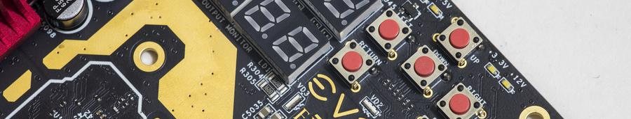
Image 13: Onboard voltage controller features
Previous generation EPOWER required external controller for real-time voltage adjustment, one of which is EVBOT. Today just few overclockers have EVBOTs, so to address this new EPOWER have onboard fully integrated controller, which allow adjustments of both voltage output channels in real-time. Voltage readouts are calibrated to DC accuracy better than 3%.
Embedded self-diagnostics
On each power up onboard controller checks all voltages, test interface operation for VRM controller and verify input signals. This takes just a moment and result of diagnostics briefly displayed on the screen. In normal conditions you should just see brief “TEST PASS” message.
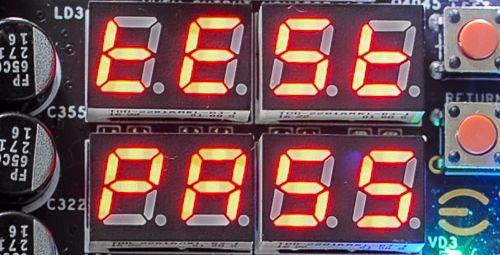
Image 14: Self-test diagnostics PASS
Future-proof USB-C interface
Onboard USB Type-C connector provide interface between EPOWER and host PC. This allow to field firmware upgrades, to support upgrades and compatibility with new graphic adapters. Update procedure is simple and involve just USB A-C cable to computer.
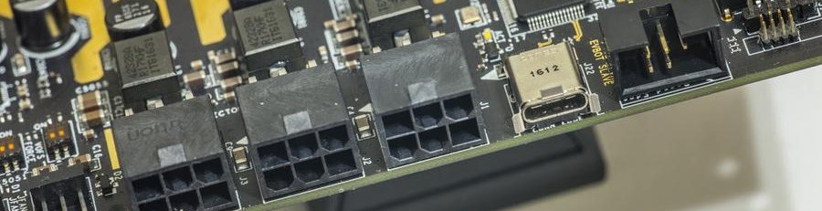
Image 15: Input and interface connectors. 6-pin power, USB Type-C and EVBOT port
ProbeIt monitoring header
Standard connector to attach external multimeter or oscilloscope for spot checks and operation monitoring. Output VCORE, Output VMEM, Onboard +3.3V, +5 and input +12V voltages are routed to ProbeIt, interleaved with ground return terminals.
Output voltage status also displayed by on-board white LED, just like EVGA GeForce GTX K|NGP|N Edition series cards.
Fan headers
Image 16: Fan headers, mode switches and input filters
Typical use case requires minimal airflow at EPOWER’s power circuits. Onboard +12V 3-pin support two fans. There is no PWM control, and fans will run 100% speed once connected to EPOWER. Unlike typical motherboard fan headers, each of EPOWER headers support high-speed high-power fans for system cooling, up to 3 A each.
Droop, Force and Offset voltage HW switches
Few advanced hardware controls available for power users. Offset switch VOFS bumps VCORE output voltage 80mV/switch, adding max voltage of 0.16V to the present value. This is independent control, handy is you needed higher boot voltage on system power on.
Force switch disable protection mechanisms to force power output, even when EPOWER overloaded.
Droop controls compensation and remote sensing operation. This is important function to compensate for voltage droop on high-power VGA’s, such as 980Ti or Titan X (Pascal).
Triple 6-pin power inputs
EPOWER V does not allow hot-plugging, hence there is no detection pin required. As result all three pairs +12V ATX PCIe Power connector, which is 6-pin MiniFit.Jr type are available as power input. Such connector configuration support 33A 12V, using typical 16AWG cables from high-end computer power supply. This is based on rather conservative +30°C temperature rise over ambient for the connector pin. In typical system, with forced airflow from cooling fans, three 6-pin connectors allow 100A+ input currents. Simple napkin power math calculation helps to understand available power budget easy:
PMAX = IMAX × V12V; PMAX = 100A × 12.0 VDC = 1200 WMAX
Where PMAX is maximum input power, IMAX current rating and V12V is input voltage from the system power supply. With help of IR3575 PowIRstage® Datasheet VRM efficiency can be estimated at level ~90%, with 94% peak at 216A load. However typical use of EPOWER will be at full loading, so calculation below is for worst case.
POUT = PMAX × 89% efficiency; POUT = 1068 W; IOUT = POUT / VOUT; IOUT = 1068 W / 1.65 VDC = 647 ADC
Where POUT is available output power with VRM efficiency in math, IOUT available current rating and VOUT typical output voltage, chosen in math above to be equal 1.65VDC. Now we can also estimate power loss on conversion.
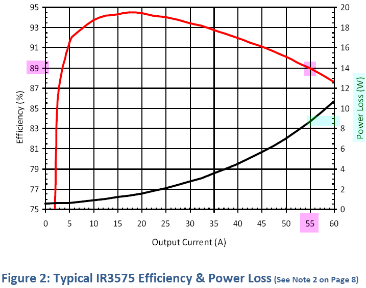
Image 17: IR PowIRstage® efficiency/PLOSS. Courtesy of Infineon/IR3575 datasheet.
At output current 647 A regulator will have 55 A per phase, which cause 9 W of power loss per phase. With total phase number equal 12 for main VOUT rail that is 9 W × 12 V = 108 W. Such power level mandate active airflow. If heatsink and PCB kept cool, IR3575 power stage silicon die temperature can be calculated using datasheet’s θJC_TOP thermal resistance specification.
Die ΔTrise = PLOSS × θJC_TOP; Die ΔTrise = 9 W × 1.7 °C/W = +15.3 °C.
With ambient temperature +30 °C die temperature will reach only +46°C, if heatsink kept at same temperature. In more realistic case, heatsink will have 30-40 °C temperature rise, which is within safe margins for IR3575 specification of TJMAX = +150 °C.
This calculation is essentially same for every DC/DC design converter, and it’s good idea to practice it for better understanding of power derating and importance of high efficiency. Such math applies to motherboard, graphic card VRMs and even ATX power supplies, if all used component specifications are known. Suggest to run own numbers with different output voltages/currents to match your case.
All three power input connectors must be plugged, as phase power balancing is done in hardware to sink current equally from each connector. Good airflow over the board is highly recommended for optimal performance with higher power levels.
EPOWER V Usage methodology
Detailed step-by-step guide in this section show typical use scenario for EPOWER V. Following the guide can help you achieve best results with this extreme overclocking product. Older guides can be used as reference as well, the overall concept and application remain the same.
To use external power regulator board, such as EPOWER V successfully follow next set of rules:
- Think carefully about the end ultimate goal, carefully and in detail. Modern graphics card VRM solutions become much better over last few years, and totally sufficient for normal use, gaming, even overclocking on water-cooling. However, to overclock card to the ultimate limit under subzero cooling with CO2 dry ice or LN2 liquid nitrogen, you may quickly run into power issues, and that’s where you consider using EVGA EPOWER V. So plan properly. It’s very unlikely that anyone would buy VGA card which was subjected to heavy PCB modifications, required to use EPOWER.
- Every power wire should have short return path wire for current. Good idea to have two return wires for every power wire. Electricity flow in closed loop circuit, using TWO wires, forward (positive VRM output) and return (GND or ground zero). This is why you always have two contacts in your home mains power outlet, not one, but two (for simplicity, earth terminal is omitted, it carries electric current only in critical failure condition).
- Keep things simple. Do not do stuff you don’t understand completely. Practice on something easy and cheap before starting complex things, and practice first on low-end old graphic cards, which you don’t care much about. Once you have solid skills to apply all required mods, proceed with higher end equipment with better skillset.
- Keep high-power paths and connections length SHORT and WIDE. More length – more voltage drop, more EMI pickup, more noise from power regulator. So lots of headache with long wires is a guarantee. This is why all power connection on VGA, Motherboards, CPU boards whatever are made with solid copper planes, to have shortest path possible for all those large currents. I would not use anything less than AWG14 for such high-power low-voltage VRMs. This rule also suggests to connect wires as close to load as possible. Usually nearest comfortable spot to connect is original VRM choke contact, from load side. You will anyway have to desolder chokes, so you already have nice solder point to start with there anyway.
5. Remember, electronics is a science about contacts. No contact where it should be – failure. Contact where it should not be – failure. Recheck and check every step of the process as you progress to get successful results. Never power up anything until it is fully checked every component and every connection. Remembering that you have only one GPU to blow up in case something goes haywire may help. These checks might feel like waste of time, delaying overclocking session by hours, sometimes even days, but it’s actually saving time, money and hardware (not by burning it, or making awful results) in long term.
KPC: Uncorking BIG KELPER – practical guide for beginners.
KPC: Using EPOWER Gen.2 on GeForce 8600 GTS card
KPC: Zombie EPOWER Titan Guide
STEP 1 – Prepare workbench area and gather all required tools
- Target device, in our case EVGA GeForce GTX 1080 Ti reference graphics card
- EVGA EPOWER V power module
- AWG12 or AWG10 copper wire with insulation or copper plates
- High power soldering iron, 120W+ recommended for copper plates
- Generic digital multimeter for resistance and voltage checks
- 80/120mm +12V DC FAN with 3-pin header for VRM cooling
- Some flux and solder for wire joints
- Insulation materials to prevent moisture on VRM
- Sharp blade to prepare insulation
- LN2 extreme cooling container for GPU cooling, such as Kingpincooling.com TEK-9 FAT
Many enthusiasts and overclockers already have most of the items from this list, only new thing – copper plates. I found them to work best than heavy gauge wires, because they are not flexible and less troublesome to keep in fixed position. However, they have large thermal mass, and need high power soldering iron, at least 120W. I use high-power ERSA iCON 1 soldering station. Also copper plates after shaping can be reused for multiple cards. Also no burning wire insulation and nasty smoke from plates, which is better for overclockers health.
Suggest to perform all modifications with good bright lights, so you can see clearly what is going on. Some additional gear, like pliers, magnifying glass, set of wires could be useful on various steps. Taking few photos during the process may help later to showcase the result in your benchmark submissions ;).
Image 18: Complete kit ready for EPOWER action
One can buy these copper sheets at local PC cooling parts shop, but pretty sure those are not hard to get all over the world in some metalwork shops, etc. Thick copper foil (0.5-1.5mm thickness) would work too, just combine few sheets together to provide nice robust plane.
When carving copper plane shapes, ensure the plane shapes are reasonably square in shape. Avoid having a long and narrow plane shape because this limits the current flow and increases plane parasitic inductance and loss.
STEP 2 – Remove onboard VRM inductors
Remove heatsink from the VGA card. It’s easy to locate power regulation circuitry on the videocard.
You can overlay EPOWER to estimate best placement on the card. It is important to keep shortest distance possible between EPOWER output exposed metal area and VGA card VRM power inductors. Short and wide connection allow better voltage regulation and stability.
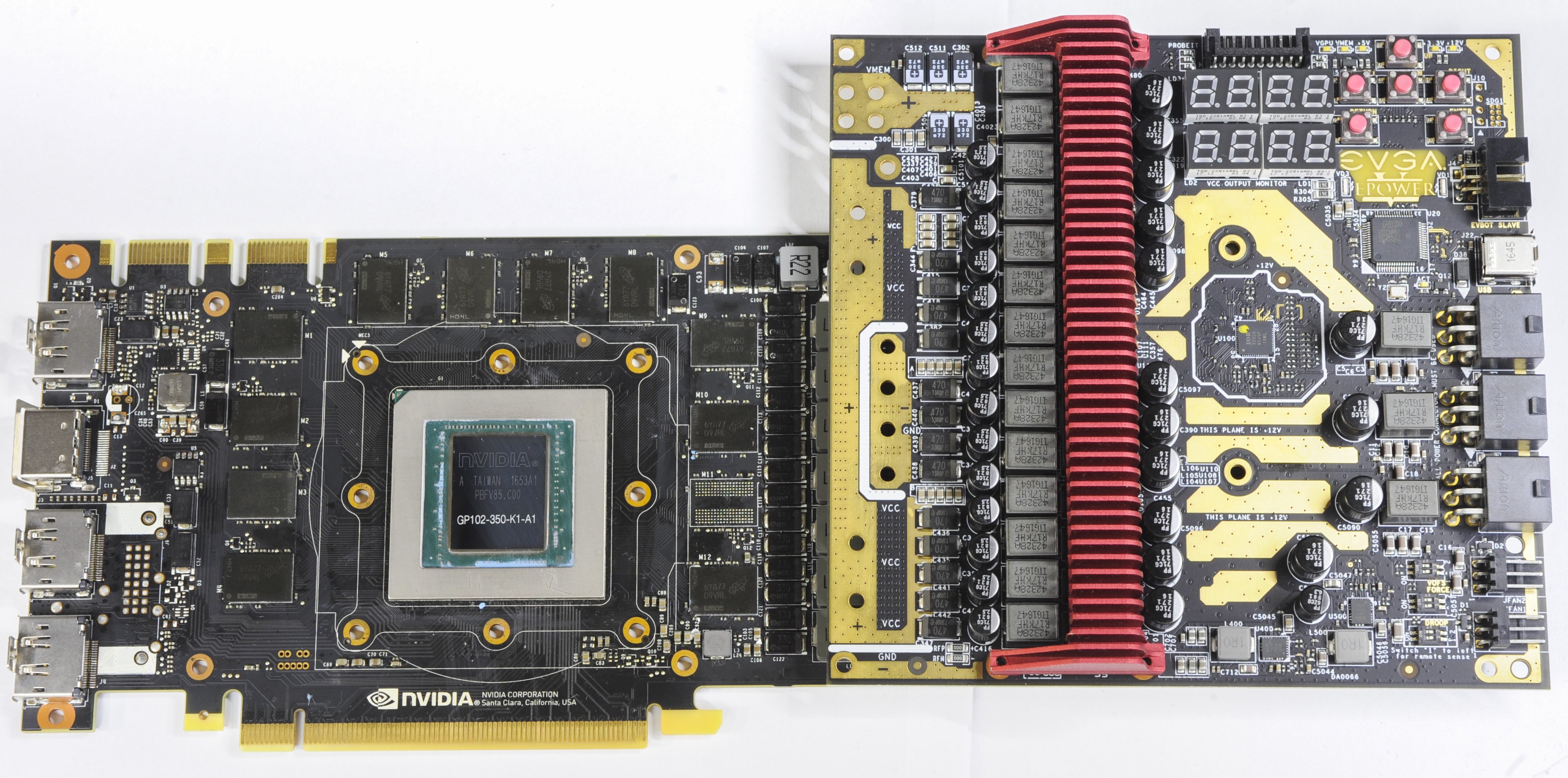
Image 19: Overlay of EPOWER Gen 5 over 1080 Ti reference GFX
Main GPU VRM circuitry usually located on the right side PCB, between GPU and power input connectors. It’s easy to spot one by location of big high-power inductors, which look like gray rectangles with two massive contacts. Now since our goal is to replace onboard power regulation circuit with EVGA EPOWER V module, we need to isolate onboard regulator, and expose copper to have clean power entry path.
At this point you can also check how much space is required for your GPU cooling solution. It would be a sad moment, if all the work done only to find out 2 mm interference with the LN2 container preventing setup from assembly.
Removing inductors (marked R22 Power choke on Image 20) will do exactly that, disconnect GPU power input from the onboard VRM and leave large area with metal plane to allow EPOWER connection. That’s where output of the EPOWER VRM will be connected once we find best spot for whole assembly.
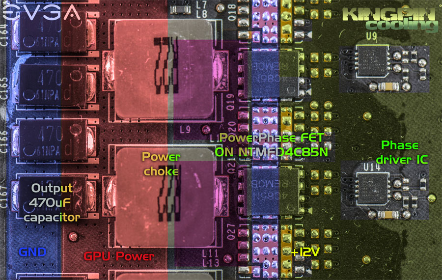
Image 20: Power train on reference GTX 1080 graphics card
Desolder original inductors of each GPU voltage phase with high-power soldering iron. On GeForce GTX 1080 Ti there are 7 inductors, marked LR22. Leave smaller R22 inductor near top edge of the board intact, that one is used for separate memory VRM circuitry.
One side of inductor pad go to VRM MOSFET stage by rather big polygon (solid copper plane) and opposite side connected across all output inductors, array of power filter output capacitors and enter internal layers to provide solid connection to GPU power pins. Idea of using EPOWER is follow same concept, so we need to connect power output from EPOWER V PCB to this output capacitor polygon as good as possible, thus having power flow into original power planes from external source.
Usually good idea to keep memory power delivered from onboard regulator. Typically, you would need memory attached to EPOWER only on older cards, or dual GPU cards to avoid power balance issues. If you decide to have memory powered from EPOWER V as well, remove memory power inductors too.
Now need to take care of PWR_GOOD signaling.
STEP 3 – Make sure PWR_GOOD is activated to allow GPU operation
Since such condition without inductors in terms of onboard VRM controller considered open phase and undervoltage fault, it will shut down output and will keep power stage FETs disabled. Exactly what we need, no need to remove other power components to disabled VRM. The only trick is that VRM controller also deactivate PWR_GOOD signal, which as we learned before will disable the GPU. So as per Image 4, cut the trace right at the VRM controller to prevent PWR_GOOD signal from it going onto the card. This sometimes can be tricky because of small trace width.
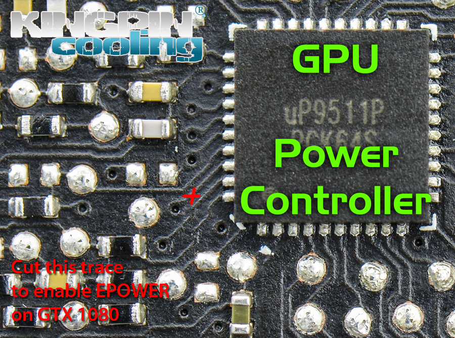
Image 21: PWR_GOOD trace cut on GTX 1080 Reference board to let GPU run w/o onboard VRM controller function
Also make sure that PWR_GOOD on the remaining trace is still activated (held high, +3.3V or +1.8V level when card is powered, with inductors removed). This step required to confirm our GPU is enabled and all it needs is actual power output from the EPOWER to be working again. If PWR_GOOD is still equal to zero, you may need to solder small 1.0…4.7 KΩ resistor to nearest +3.3V point. You can trace +3.3V by probing PCIe +3.3V pin and components near VGA’s VRM controller with DMM, set to lowest resistance measurement range, such as 200 Ω.
For more details on which trace is PWR_GOOD (sometimes called VR_RDY or READY, depends on controller) on specific card try to find datasheet for the specific controller used on your card, or consult with all-knowing Internet.
Memory VRM may also have same PWR_GOOD signal, that can enable/turn on secondary VRMs, such as PEXVDD. Make sure that one is correct as well. If it’s not high +3.3V/1.8V when card is powered on, add a pull-up resistor as described above. You must have all rails operational at power on, otherwise GPU will not start.
STEP 4 – Expose copper plane for ground and power on target device
Now we removed onboard inductors, ensured correct level of PWR_GOOD signal and ready to proceed for additional copper cleaning to get larger soldering area to EPOWER. More surface area between VGA and EPOWER improve connection quality and reduce unwanted parasitic resistance. Do not skip on this step, as even small resistance increase of 10 mΩ can cause significant voltage losses and issues at high current levels. Modern GPUs can easily sink currents over 200-400 A under extreme overclocking conditions, or even more in short peaks under heavy load!
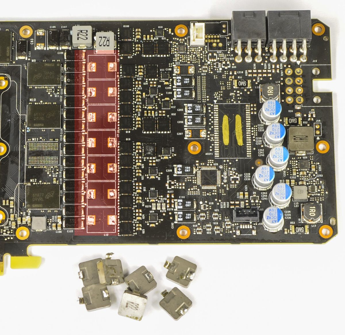
Image 21: Power train on reference GTX 1080 Ti graphics card
Solder mask is hard coating on the PCB surface that protects outer copper layer and provide electrical insulation to avoid shorts. On VGA this mask often colored black, but it can be different colors. Mask coating is chemically and mechanically robust, so typical solvent such as acetone or IPA will not be able to remove it.
Easy way to remove mask is use mechanical tools to remove thin layer, exposing bare copper metal for soldering. Inspect the area carefully, to ensure there are no isolated via (PCB pad with metallized thru-hole drill) for other signals. We need expose copper connected to GPU power. Best area to start with is outputs of the inductors (left pad on Images 21,22).
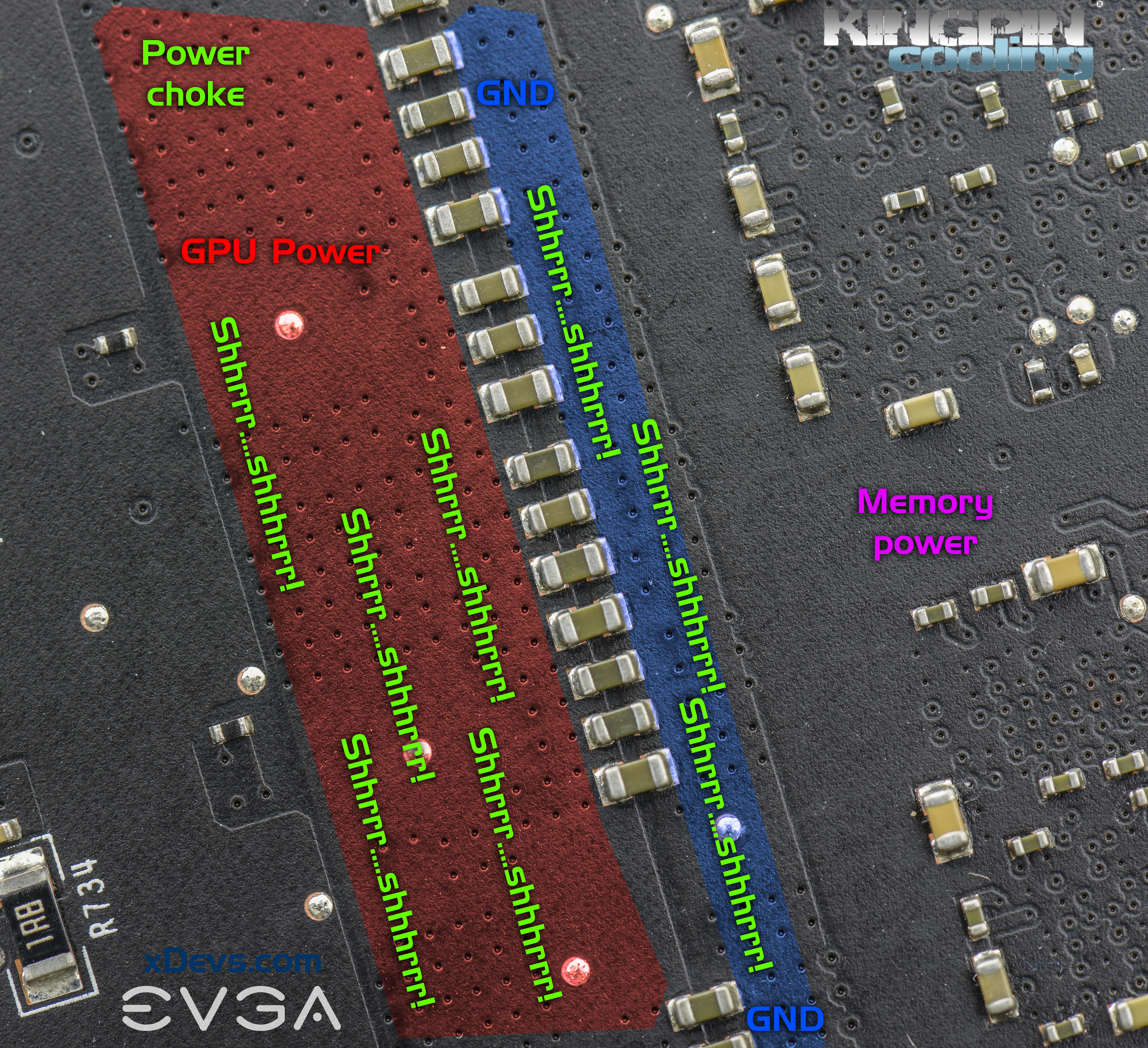
Image 22: Bottom side area on GTX 1080 graphics card, can be used for additional connections
You can use any tool suitable for scratching etc. While it’s OK to do so with sharpie, it’s possible with careful use of small grinder, such as Proxxon FBS 115/E with sandpaper cylinder tool on it.
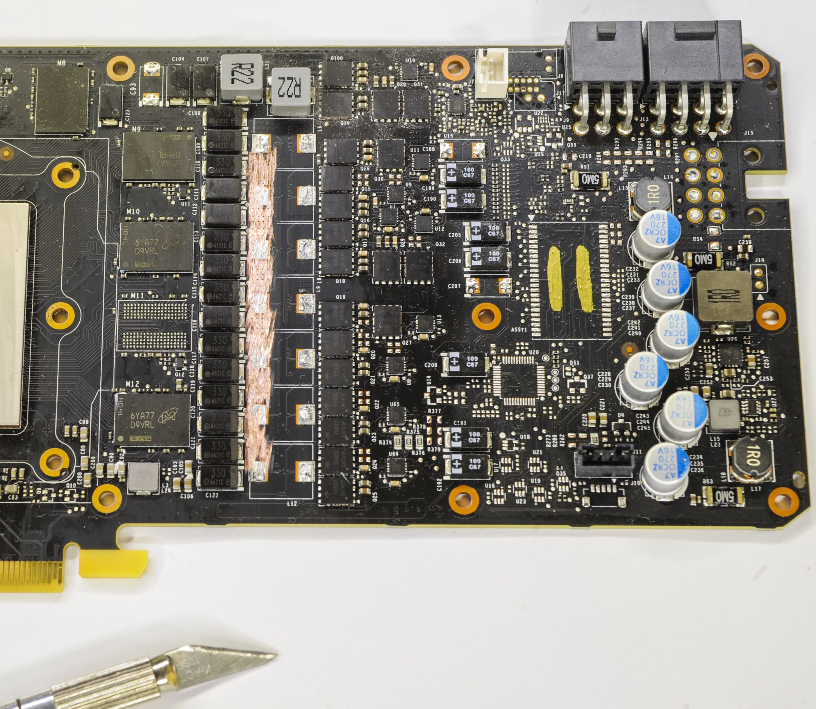
Image 23: Power train on reference GTX 1080 Ti graphics card
Take care not to expose or short any other traces on PCB, or you will need to repair broken connections. Use minimal speed and avoid applying force, to reduce risk of knocking off nearby PCB components damage or going too deep into PCB layers. After some “shhrrr-shhrrr” action, you should have nice and shiny clean copper surface on power plane, ready for soldering.
If you connecting memory power to EPOWER, expose memory copper plane same way.
STEP 5 – Solder the EPOWER down to the card
Good rule to follow: one pair of wires (VCORE+GND) per each 10-15A of estimated current. For simple VGA with 2-3 phase VRM best to use 4-8 wire pairs. For high-end VGA should be no less than 12-16 wire pairs. Top GPUs like GK200, GM200, GP102 you must use as many pairs as possible physically or solid copper planes.
Solder thick (AWG10-AWG12) wires or 0.5-2mm solid copper plate from EPOWER V GND to ground areas on card and VCC points to power plane. Ground can be probed by DVM in resistance mode, by reading less than 0.1 Ω between outer metal shells of DVI/HDMI connectors. Use the relative measurement to shorted probes, to null the resistance of the probe leads. If your DMM does not have the relative measurement mode, just short probes together in lowest resistance range and subtract resulting reading later from the actual measurement to obtain true resistance on PCB. Use sharp and clean probes for good contact.
In the end result you may end up with something like on Image 24.
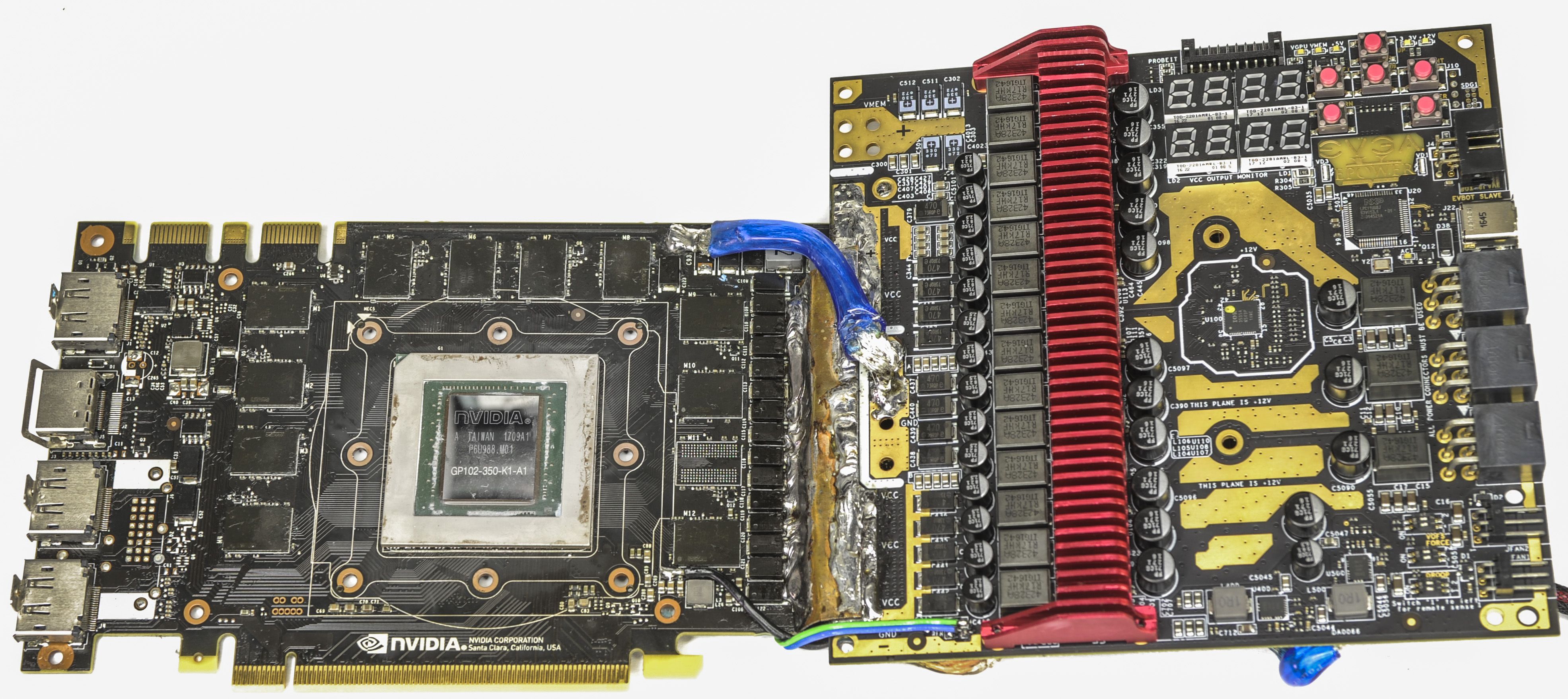
Image 24: EPOWER V attached to GTX 1080 Ti reference board
Note solid copper connection for the VCORE output between EPOWER and VGA card. Blue AWG8 cable provide additional ground connection. There are more of these wires between EPOWER and the card.
Keep in mind that once you soldered EPOWER on the card, you will lose access to the front side of the reference PCB. This means adding any reworks or modifications in area under EPOWER would be extremely difficult. So add wires and other modifications, like memory mod, power mods BEFORE you solder EPOWER.
After connecting EPOWER V to GPU always check the resistance between power and GND to ensure there are no shorts. Normal resistance range for a GPU is 0.4-10 Ω depending on GPU, for memory – 10-200 Ω. If you get very different resistance readings, you card is likely borked and game is over. Well, not really, you just need to find short between power and ground and fix it.
Same process applies to memory power, if you use it from EPOWER. If wires and connections between VCORE and VMEM outputs are too close, check the resistance to make sure there is no short between power rails.
Also here are some useful reference points, key resistance values measured with high-accuracy Keithley 2002 DMM on good working card:
| GPU | Voltage rail | Resistance measured | Nominal voltage |
| 1080 | NVVDD | 80-250 milliΩ | 0.64 VDC … 1.1VDC |
| FBVDD | ~97 Ω | 1.35 VDC fixed | |
| PEX | ~44 Ω | 1.02 VDC fixed | |
| MEMPLL | ~450 Ω | 1.80 VDC fixed | |
| 1080 Ti/Titan Xp | NVVDD | 40-180 milliΩ | 0.64 VDC … 1.1VDC |
| FBVDD | ~80 Ω | 1.35 VDC fixed | |
| PEX | ~80 Ω | 1.02 VDC fixed | |
| MEMPLL | ~460 Ω | 1.80 VDC fixed | |
| 980 Ti | NVVDD | ~1.5-5 Ω | 0.7 VDC … 1.21VDC |
| FBVDD | ~15 Ω | 1.50 VDC fixed | |
| PEX | ~200 Ω | 1.02 VDC fixed | |
| 980 | NVVDD | ~3.5-8 Ω | 0.7 VDC … 1.21VDC |
| FBVDD | ~30 Ω | 1.50 VDC fixed | |
| PEX | ~180 Ω | 1.02 VDC fixed | |
| 780 Ti | NVVDD | ~1.5-4 Ω | 0.8 VDC … 1.23VDC |
| FBVDD | ~55 Ω | 1.50 VDC fixed | |
| PEX | ~160 Ω | 1.02 VDC fixed |
Table 2: Nominal resistance on main power rails from good GeForce GTX cards
Also I have collection of resistance measurements on legacy graphic cards, listed here.
STEP 6 – Final check and first power on
After obtaining good results on resistance check, you can go ahead with final checks and mounting cooling system on the GPU. Insulate PCB from water condensate by preferred way, same as you would do with normal LN2 session. Keep moisture away from the EPOWER V card and ensure that there is no direct contact with frozen areas on target device.
EPOWER V card also requires airflow under heavy load conditions, get some 80-120mm sized DC fans ready. EPOWER provide two 3-pin FAN connectors, each can provide 3 Amps at +12 V.
Install zombie card into the PCIe slot, make sure no metal parts touching the EPOWER PCBA. Connect PCI-Express power 6-pin/8-pin cables to BOTH EPOWER V card AND videocard. This will provide power and ground to the VGA, as most cards still need to have +12V present for auxiliary circuits and detection logic to work properly. Default startup voltage for EPOWER rails is +0.9 VDC for VCORE and +1.35 V VMEM. Preset voltage levels fit modern GPUs like 980/980Ti/1080/1080Ti/Titans.
Now turn system on, and check all the voltages. If power on voltage is OK and there is no smoke coming out of nowhere. but system does not detect videocard – make sure PWR_GOOD signal from onboard VRM controller on videocard is isolated, and it’s GPU side is indeed +3.3V. If it’s low (0V) GPU will be kept in reset (because onboard power is not used – it’s fault state for it).
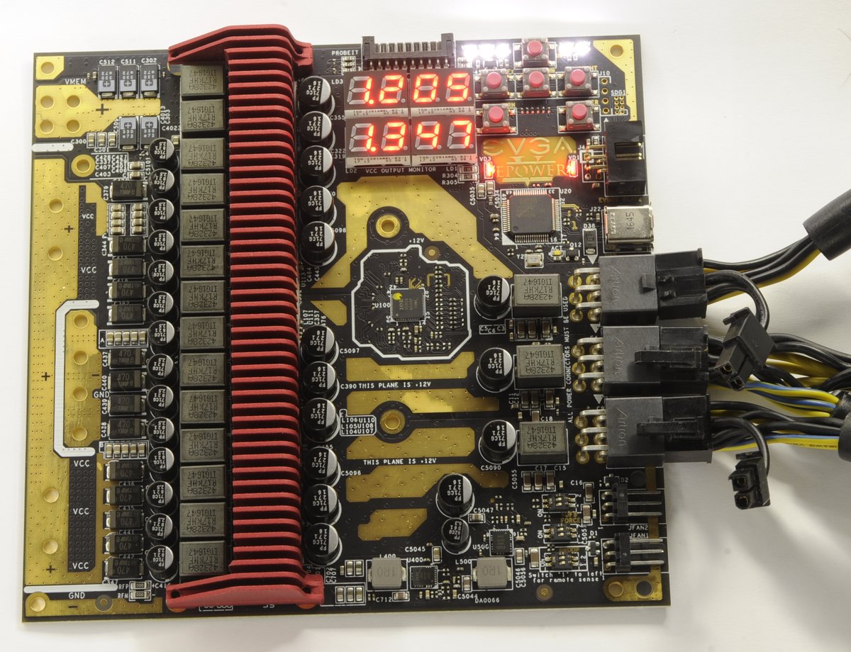
Image 25: Normally working EPOWER V with onboard voltage display
EPOWER does a quick self-check every power on, and then automatically switches outputs ON. If everything OK, it will display current output voltages on LED display, like displayed on Image 25.
EPOWER output voltage control
Voltage control is easy and straight-forward. There are six buttons on top right corner of the board, which allow to perform all essential adjustments.
- UP – Increase value by one digit.
- DOWN – Decrease value by one digit
- LEFT – Move cursor 1 position left, highlighted by decimal dot on display.
- RIGHT – Move cursor 1 position right, highlighted by decimal dot on display.
- ENTER – Apply new value to EPOWER output
- RETURN – Reset voltage to 0.9 V / 1.35 V levels.
Both displays are controlled by same buttons, cursor for selected digit will automatically switch once you press LEFT (or RIGHT) in most significant digit of the previous display.
Voltage is applied immediately on ENTER keypress, but return to monitoring mode (when both VCORE and VMEM actual voltages are shown) will occur after few second delay.
Monitoring mode is also indicated by red color for LEDs near EPOWER logo. In setting mode color change to green.
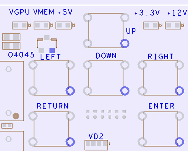
Image 26: EVGA EPOWER V onboard keypad
Allowed output voltage range for each rail shown in table below:
| EPOWER V rail | Specification | Value | Unit |
|---|---|---|---|
| VCORE | Minimum output voltage | 600 | mVDC |
| Default output voltage | 900 | mVDC | |
| Maximum output voltage | 2000 | mVDC | |
| Maximum output current | 620 | A | |
| Setting accuracy, maximum | 3 | % | |
| Monitoring accuracy, maximum | 1 | % | |
| VMEM | Minimum output voltage | 600 | mVDC |
| Default output voltage | 1350 | mVDC | |
| Maximum output voltage | 2200 | mVDC | |
| Maximum output current | 90 | A | |
| Setting accuracy, maximum | 3 | % | |
| Monitoring accuracy, maximum | 1 | % |
Table 3: Output ranges and settings
These values are valid for the default condition out of the box, measured at the output of the EPOWER V card.
Hardware monitoring options
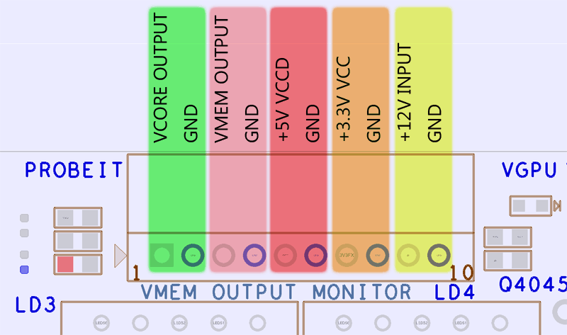
Image 27: EPOWER V monitoring ProbeIt connector for external DMM/scope
You can use ProbeIt adapter from EVGA Dark motherboard or Kingpin Edition VGA to your usual multimeter probes, or in case you want to have custom cable connection to your specific meter, you can grab connector separately, for example here from Digikey.com. You will also need these contacts. If you want less pins (for example only 4 to monitor GPU and MEM voltage) you can get needed housings right here .
| Pin number | Signal name | Example photo |
|---|---|---|
| Pin 1 (square) | VCORE output voltage | 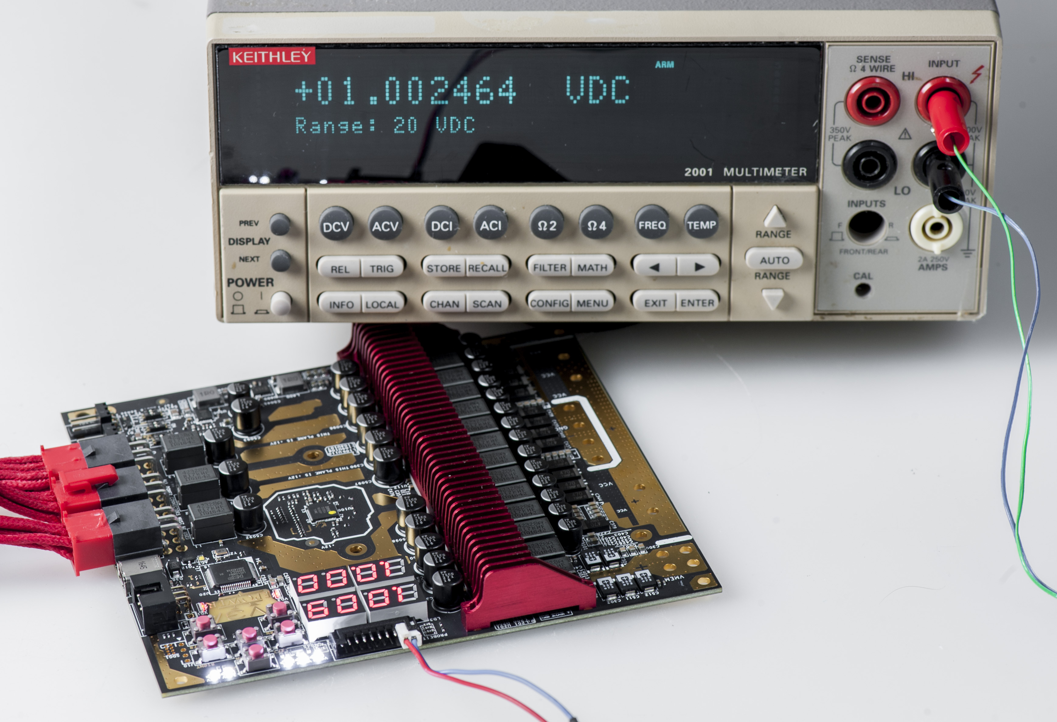 |
| Pin 2 | Ground | |
| Pin 3 | VMEM output voltage |  |
| Pin 4 | Ground | |
| Pin 5 | Onboard +5V voltage | 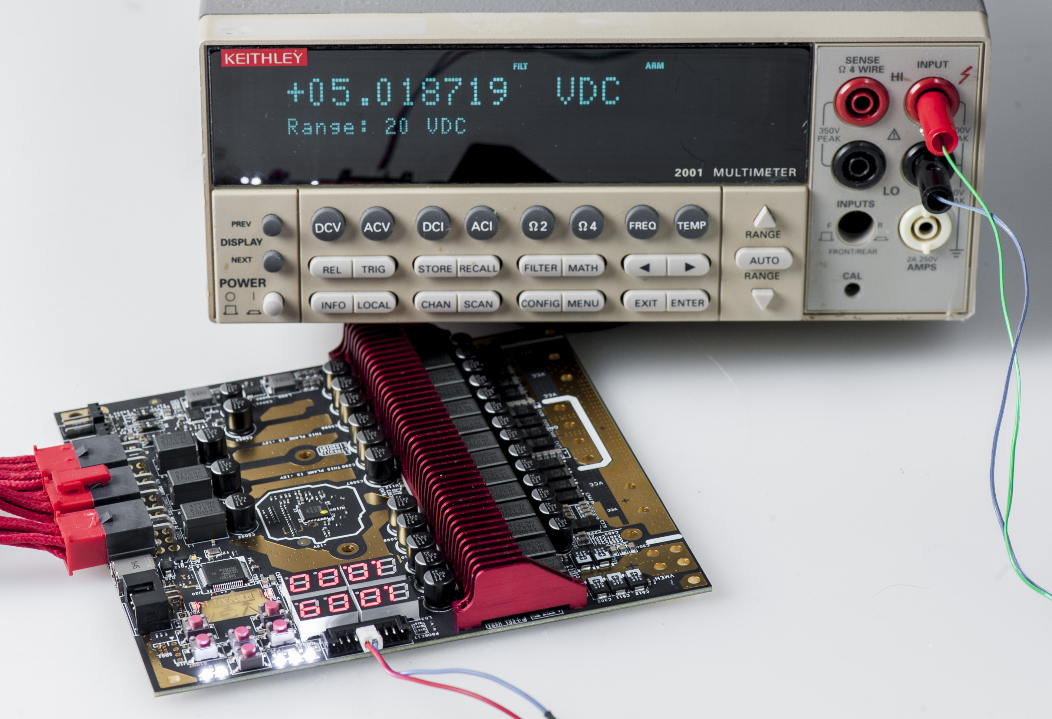 |
| Pin 6 | Ground | |
| Pin 7 | Onboard +3.3V power voltage | 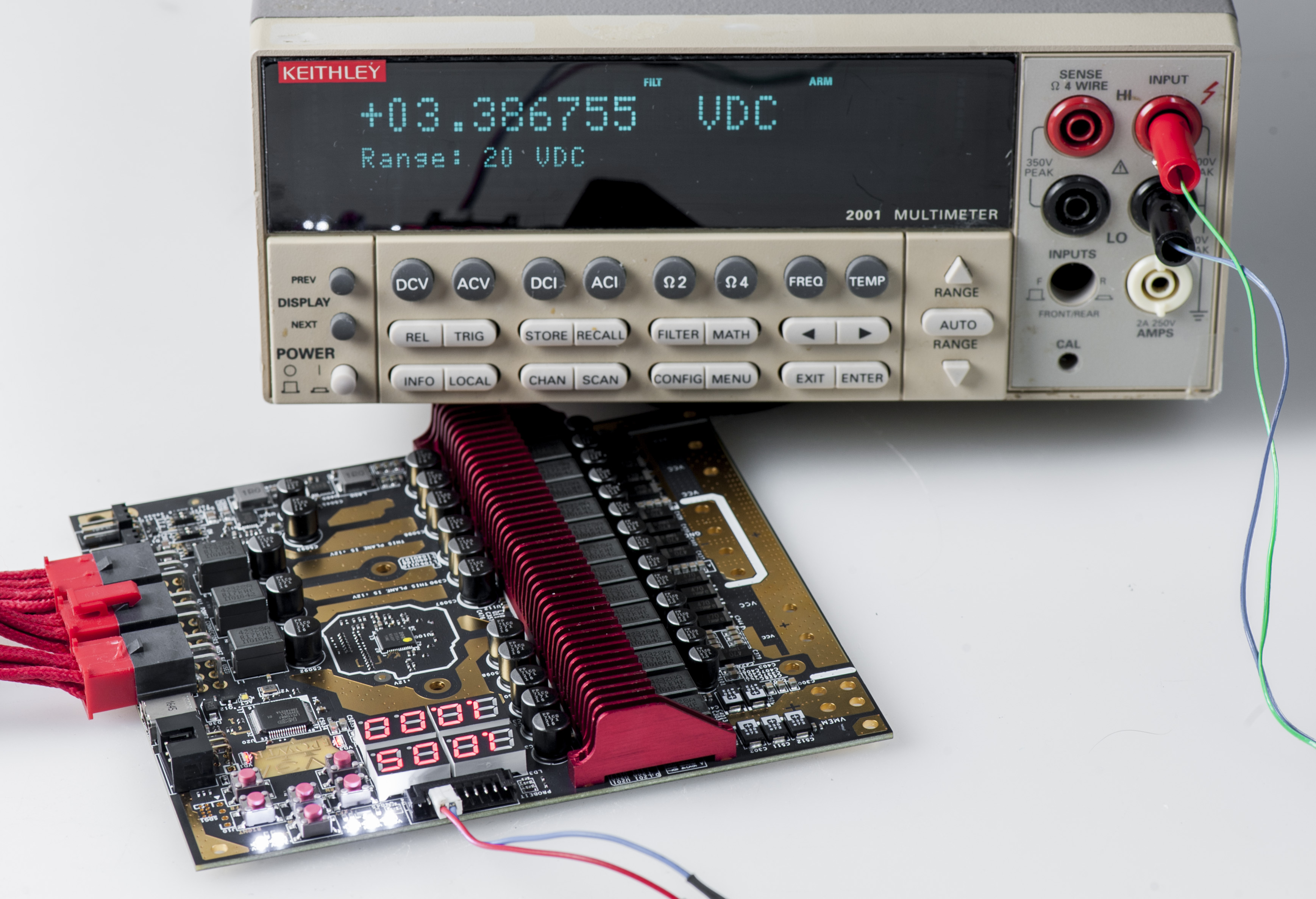 |
| Pin 8 | Ground | |
| Pin 9 | Onboard +12V PCIe power voltage | 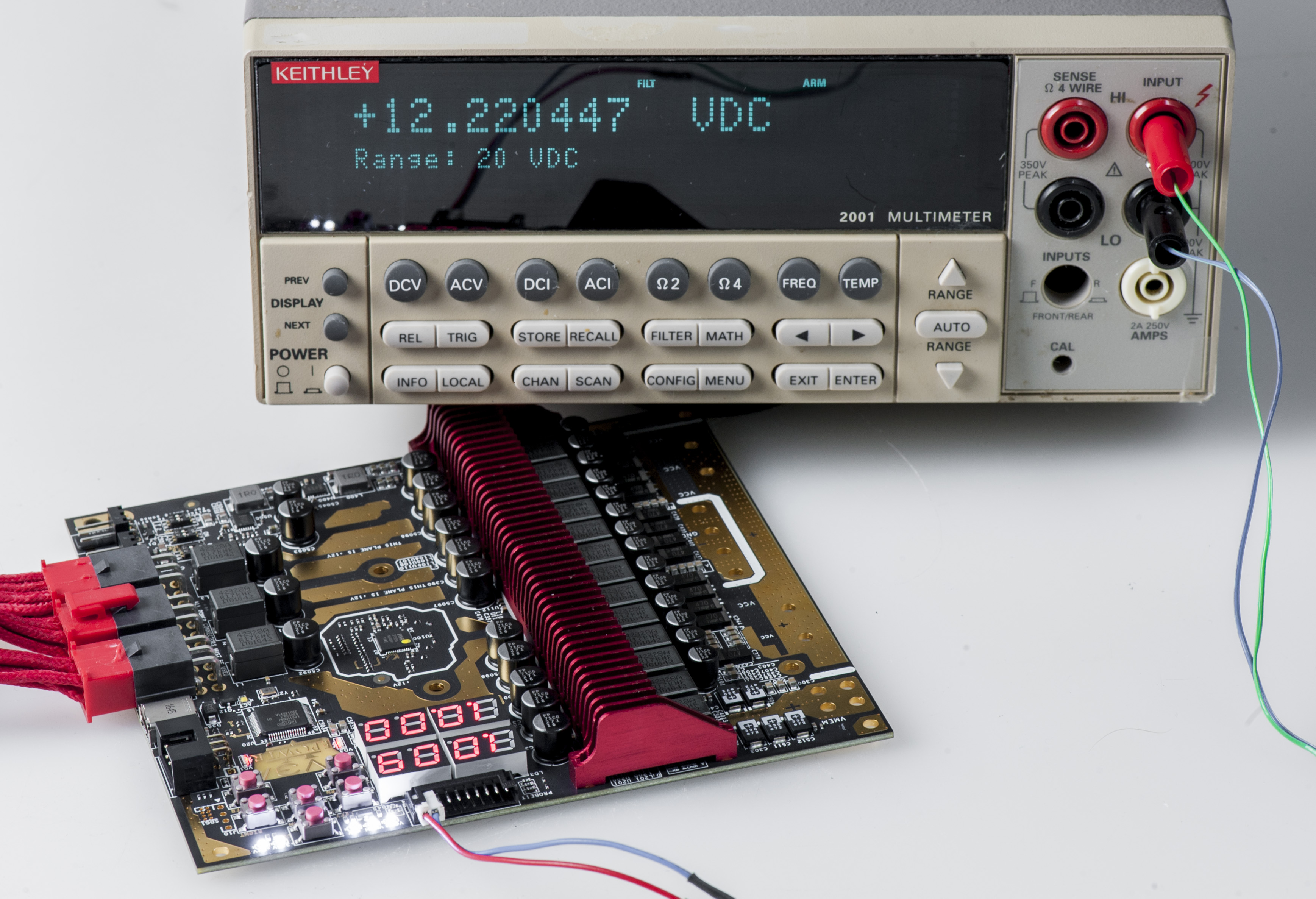 |
| Pin 10 | Ground |
Table 4: ProbeIt header definition on EPOWER V
Pinout for this header follows other EVGA OC targeted projects, and shown in Table 4. All voltage outputs from ProbeIt heaters are protected by onboard fuses to ensure safe probing. Same pin definition legend is printed on the bottom side of the EPOWER board.
Also five white LEDs near the PCBA edge allow to monitor the voltage health in realtime. Their definition and function is same as older Classified/KINGPIN cards. If any of the LEDs not on, the voltage rail is absent and system/EPOWER may require troubleshooting.
Onboard switches to control EVGA EPOWER V settings
Set of three dual-position switches control advanced features, such as fixed voltage offset, VRM protection override and remote sense function.
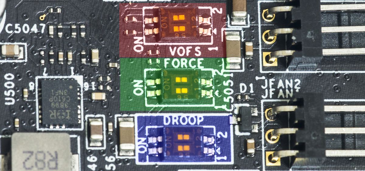
Image 28: EPOWER V onboard hardware configuration switches
Top to bottom they are labelled VOFS, FORCE and DROOP. Factory default setting for all switches is OFF, with slider position to the right side. Status and function map for all these presented in table below. Different switch functions can also be used in conjunction.
Voltage increase method is bit different to software or onboard EVBOT override control as an offset is applied at any programmed voltage. It could be useful if you wanted test little bit extra voltage for experiment, without changing programmed setting. Each offset VOFS switch position at ON will add +80 mV, so both will give +160 mV.
| Output voltage offset | DIP switch VOFS position (marked red on Image 28) | |
| 1 | 2 | |
| +0 mV | OFF | OFF |
| +80 mV | OFF | ON |
| +80 mV | ON | OFF |
| +160 mV | ON | ON |
Table 5: VOFS Switch function defines on EPOWER V
Second switch, marked green on Image 28 is for protection override, and would rarely be needed for typical LN2 overclocking. If you suspect that power loss occur due to OCP (which is set really high on EPOWER V), you may try to toggle FORCE switch position to ON and back to OFF to attempt a power reset.
| Override safety | DIP switch FORCE position | |
| 1 | 2 | |
| Safe mode | OFF | OFF |
| Main VCORE output controller force ON | OFF | ON |
| Secondary VMEM output controller force ON | ON | OFF |
| Both outputs forced to be always ON | ON | ON |
Table 6: FORCE Switch function defines on EPOWER V
Last, but not least DROOP switch. Default “OFF+OFF” setting tells controller to regulate voltage to the programmed value right at the EPOWER board, without taking any loading into account. Let’s imagine simple example, VCORE programmed to 1000 mV. With this setting EPOWER’s VRM controller will continuously monitor output voltage at EPOWER and adjust switching operation of PowIRStages accordingly to get matching 1000 mV. So the whole system forms a closed feedback loop that maintains stable output. This also mean that VRM controller does not “see” the loading, so if there is a voltage drop on connection wires and reference board PCB equal to 100mV, actual GPU core will get only 1000 mV – 100 mV = 900 mV.
| Output voltage offset | DIP switch DROOP position (marked blue on Image 28) | |
| 1 | 2 | |
| EPOWER Standalone compensation, max vdroop | OFF | OFF |
| -50% vDroop setting | OFF | ON |
| -50% vDroop setting | ON | OFF |
| Remote compensation, using RFP/RFN resistors | ON | ON |
Table 7: DROOP Switch function defines on EPOWER V
Now middle settings with either of the switches set to ON will add spacing between sense points so there will be some impact from loading current. In same example VRM will sense some of voltage drop due to loading, and will attempt to compensate by overshooting the output voltage. So with programmed 1000mV setting you may get actual 1050mV, as 50mV loss was accounted for. As result 1050 mV – 100 mV = 950 mV, so GPU will get closer voltage to the setting.
Remote sense option for maximum control over voltage drop
Remote compensation takes this concept to the extreme end, meaning that VRM will ignore onboard voltage at EPOWER and measure the output voltage for compensation at resistors RFP/RFN. Sometimes it is also desired to have fine control over feedback and voltage control under load. To provide best experience with EVGA EPOWER V, flexible remote voltage sense operation is allowed. To fully utilize remote sensing, you need to desolder these two resistors (they are 0 Ω SMD1206 shorts). Two resistors are installed on the EPOWER PCB by default, just near the bottom left edge.
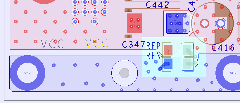
Image 29: EPOWER V remote sense points
Top resistor RFP is providing positive (+) signal to the VRM controller (gray pad on Image 29), while symmetrical RFN is providing negative return (−). To compensate on remote location, connect twisted cable (for example two wires from Cat6 Ethernet cable) and solder them to the points on the reference board attached to EPOWER. Maintain correct polarity, meaning that positive VCORE connection must be connected to RFP gray pad, and nearest GND return must be connected to RFN gray pad. As result any voltage droop between EPOWER and sense points would be eliminated by the output overdrive. Sense wire is visible on the Image 24 presented above in this article.
For example, to completely eliminate voltage droop you can route sense wires right to the capacitor + and – pins in area behind GPU on back side.
- Remove RFN and RFP zero ohm (short) resistors
- Solder twisted wire pair to right points (gray pads) of RFN and RFP
- Connect RFP wire to +Vcore on VGA copper plane point
- Connect RFN wire to -GND on VGA copper plane point
Make sure your sense wiring is correct, and right RFP pin is connected to positive sense point on target device (+Vcore). Right RFN must be connected to negative sense point on target device (GND). If connection get broken output voltage will be unregulated, which can damage your graphics card or/and EPOWER!
In same example as above math calculation with look like 1100mV – 100 mV = 1000 mV. This meaning that GPU will have same voltage delivered as the programmed setting. If you connect to different locations +/− on reference PCB, you can get effect somewhat in between, with just medium droop compensation. Experiment on your specific setup to find what gives best overclocking results, as there is no universal rule that match every GPU.
Remote sense function can help to mitigate issues due to smaller/weaker connection between EPOWER and VCORE, but it must be applied with care, as there are limits when compensation cannot work reliably anymore. In typical setups VRM can handle around 250mV maximum of voltage droop between EPOWER and sense point. If actual voltage loss is larger, you must add more wires/copper between boards.
Switches can be adjusted any time and work separately from digital controls, due their hardware function nature.
Firmware update procedure and available firmwares
As EPOWER target audience is usually experienced overclockers, firmware upgrade procedure is available now to provide even greater control on EPOWER functionality. Firmware update workflow shown in list below:
- Connect all three 6-pin PCIe Power plugs from PSU.
- Connect EPOWER interface port USB Type-C to your Windows-computer.
- Extract contents of firmware archive to empty directory.
- Run DFUAPP.exe tool. This tool has simple GUI to allow download and uploads of the EPOWER firmware.
- Hold RETURN key and power on the PSU with EPOWER connected.
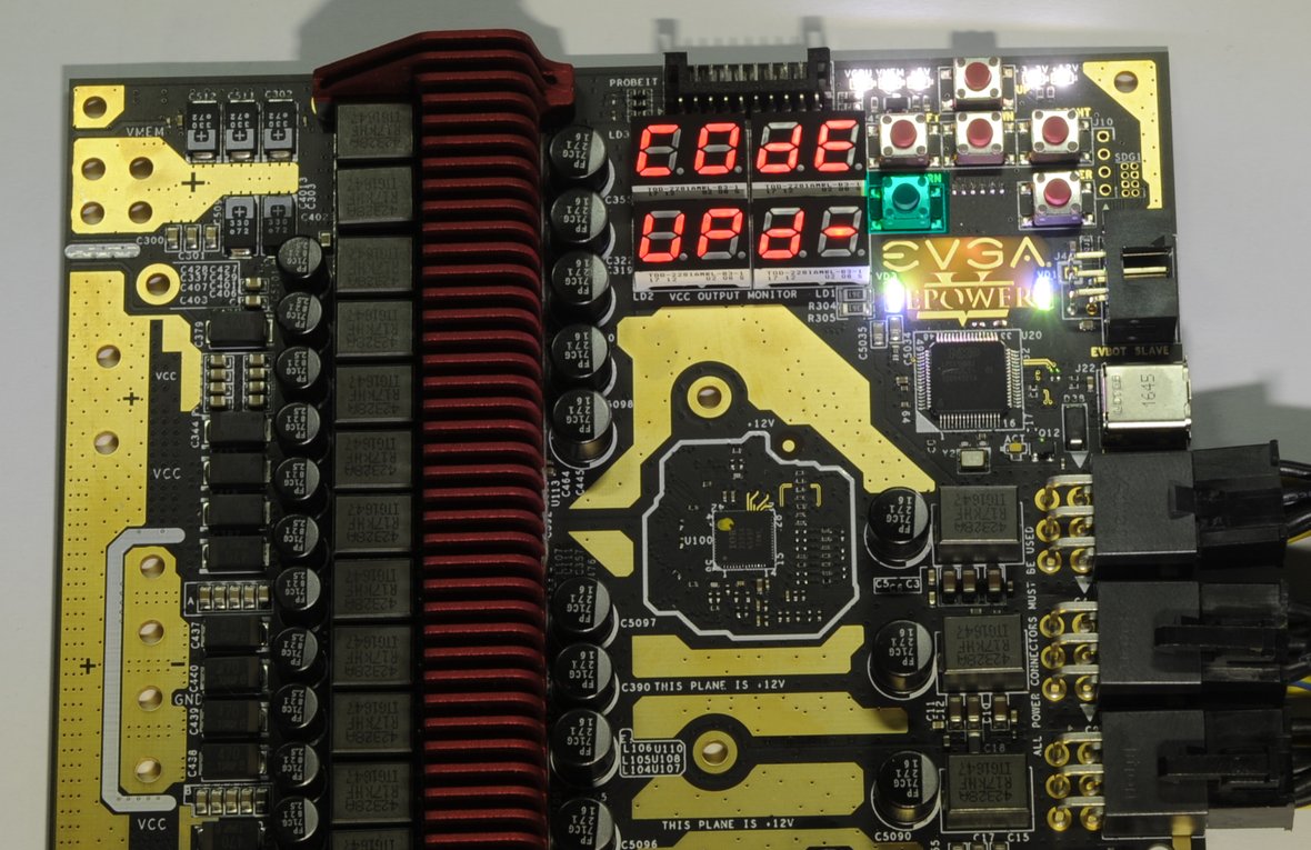
Image 30: EPOWER V in firmware code update mode
EPOWER should show CODE UPD- message on the LED display, and DFU application should be able to detect connected EPOWER
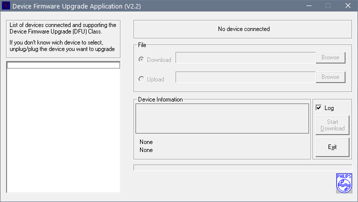
Image 31: EPOWER V detected by firmware update DFU tool
- Select firmware .bin file from the file in Download section.
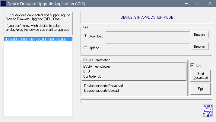
Image 32: EPOWER V detected by firmware update DFU tool
- Press “Start Download” button to update code in EPOWER with selected binary file.
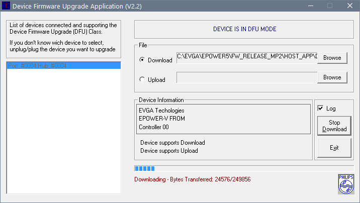
Image 33: EPOWER V detected by firmware update DFU tool
Now DFU tool will upload the code into EPOWER controller. During the process you will see CODE UPD- LED display message flashing, that is expected.
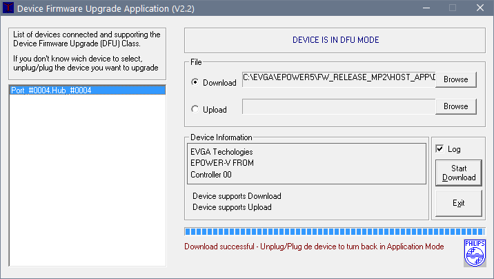
Image 34: EPOWER V detected by firmware update DFU tool
Once completed, you will be greeted with “Download successful” message.
- Unplug USB cable and power cycle the EPOWER.
Available firmware list provided in Table 8.
| Firmware for EPOWER V | Best works for GPU | Default Vboot | DFU Tool + firmware binary archive | File CRC32 Checksum |
|---|---|---|---|---|
| EVGA EPOWER V, Rev.52a | GTX 1080/1080Ti/Titan X(Pascal) | 0.9 V / 1.35 V | RAR SFX-archive | 2DFECD54 |
| EVGA EPOWER V, Rev.52b | GTX 980/980Ti/Titan (Maxwell) | 1.2 V / 1.50 V | RAR SFX-archive | 4FB21602 |
Table 8: Firmware packages for EVGA EPOWER V
DFU tool allow any direction upgrade, both from newer version to older, and from older to newer.
Software toolkit
EPOWER also have legacy EVBOT connector for interfacing other EVGA Devices or EVBOT controller.
Overclocker 1whiteshark1 from hwbot actually found console menu, one similar to 980 Ti Kingpin Edition. He prepared rather nice detailed tutorial how to use it, which I mirror here as well.
PDF-tutorial of EVBOT voltage control serial menu
You would need USB to UART interface dongle and terminal programm, such as PuTTY to use this interface.
Conclusion and feedback
Hope this will help to get better overclocking and world records out of your hardware, with no more power delivery issues or limitations. If you find errors or have issues using your EVGA EPOWER V, feel free to leave a comment here or in discussion thread at Kingpincooling.com forum.
Modified: June 10, 2019, 1:14 a.m.