Contents
- Disclaimer
- Introduction
- Project and design specification
- Build worklog
- Calibration
- Performance and test examples
- Final note and summary
Disclaimer
Redistribution and use of this article or any images or files referenced in it, in source and binary forms, with or without modification, are permitted provided that the following conditions are met:
- Redistributions of article must retain the above copyright notice, this list of conditions, link to this page and the following disclaimer.
- Redistributions of files in binary or source form must reproduce the above copyright notice, this list of conditions, link to this page, and the following disclaimer in the documentation and/or other materials provided with the distribution, for example Readme file.
All information posted here is hosted just for education purposes and provided AS IS. In no event shall the author, xDevs.com, or any other 3rd party be liable for any special, direct, indirect, or consequential damages or any damages whatsoever resulting from loss of use, data or profits, whether in an action of contract, negligence or other tortuous action, arising out of or in connection with the use of any information published here.
Introduction
Back in 2008, when I was still a student, for better learning of computer systems operation and embedded devices development, I started this project. There was need of testing high power (up to 2000W, +12V DC) switching power supplies, used in desktop computers. Project goal was to build automatic power supply testing unit, or like how they usually called – ATE. Of course, there are production systems from leading vendors, such as Chroma ATE or HPAK, but those are out of scope and price reach for small labs.
Why someone would need automated machine? Well, if you design power supplies or want to test existing power supply, you must have easy adjustable loading for PSU, so you can stress power supply and ensure its proper operation, both thermally and electrically. Of course, job can be done with instruments like standalone DC loads, multimeters and oscilloscopes to measure add data, and evaluate actual PSU performance on output voltage power rails, but if you need test power supplies every day, or have more than two channels on them, just wiring and adjusting knobs and buttons on test gear become very time ineffective. Humans are not designed well to do repetitive monotonic job for long periods of time, while computers and robots are don’t care at all, and can do testing much faster and with good repetitive rate.
There is nothing better for learning new stuff than actually trying to build something. It’s even better when first design fails. This leads good engineers to study more about the subject and find an exact reason why something failed. Theory backed up by practical engineering is always a great value for every practical application.
Project and design specification
First step of any design, either be it simple circuit with 5 components, or complicated machinery with hundreds of parts, megabytes of firmware and software code in it always should start with a definition of specification. What device will be doing? How it should do it? What way user can control its operation and settings? How to read results and data out of it? Does protection on input signals need to be implemented? If answer is positive, then how well signal should be protected? This are common questions need to be addressed in specification.
Let’s define, what power supply tests should this ATE perform. ATX Power supply design guides give a good idea how PSUs are tested by design and manufacturers. We can use it as a base reference. This gives us next required features:
- Test for reliable power-on/off operation at AC loss events
- Load regulation, both individual per channel and overall
- Stress-test with constant load over long time
- Power supply efficiency (if we can measure input power)
- Protection testing (overload, overcurrent)
- Dynamic loading test (variable load over time)
- Digital logic test (PowerON/PowerGOOD)
- PSU Power on delay time test
- PSU test with close to real application conditions (desktop PC chassis with elevated thermals)
Our operation conditions are defined as:
- Mains power, 110-240 VAC, 50-60Hz, 3A
- 100% IBM-compatible PC with Windows 2000/XP/2003/Vista/7/8/8.1/10 for control and data processing
- Ambient temperature (operation), 0…+50°C with power levels 800W
- Ambient temperature (operation), 0…+40°C with power levels 1200W
- Ambient temperature (operation), 0…+30°C with power levels 2000W
Relaxed ambient temperature spec will allow using cheaper power components for DC load channels, so some cost can be saved. Unit not intended for tight equipment racks, where cooling usually an issue, so we can try to get away with this spec.
Since majority of ATX power supplies are using standard connectors, I choose to have next input interfaces for interconnection with PSU:
| Input port | Type | Voltage channels |
|---|---|---|
| MiniFit-JR SYS | ATX 24-pin | SYSTEM, +3.3V,+5V,+5Vsb,+12V1, -12V |
| MiniFit-JR CPU0 | ATX12V 8-pin | CPU0 (black, primary, two +12V1&2 channels) |
| MiniFit-JR CPU1 | ATX12V 8-pin | CPU1 (white, secondary, two +12V5&6 channels) |
| MiniFit-JR VGA1 | 6+2-pin | PCI-e graphics power input, +12V1 |
| MiniFit-JR VGA2 | 6+2-pin | PCI-e graphics power input, +12V2 |
| MiniFit-JR VGA3 | 6+2-pin | PCI-e graphics power input, +12V3 |
| MiniFit-JR VGA4 | 6+2-pin | PCI-e graphics power input, +12V4 |
| MiniFit-JR VGA5 | 6+2-pin | PCI-e graphics power input, +12V5 |
| MiniFit-JR VGA6 | 6+2-pin | PCI-e graphics power input, +12V6 |
| MiniFit-JR VGA7 | 6+2-pin | PCI-e graphics power input, +12V7 |
| MiniFit-JR VGA8 | 6+2-pin | PCI-e graphics power input, +12V8 |
Table 1: Input connectors and channel definition
This brings us next requirements for individual voltage channels:
| Channel number | Voltage | Range | Max current | Max power | Definition |
|---|---|---|---|---|---|
| Voltage channel 1 | +3.3VDC | 0-6V | 25A | 150W | System +3.3V |
| Voltage channel 2 | +5VDC | 0-6V | 25A | 150W | System +5V |
| Voltage channel 3 | +5VSB | 0-6V | 10A | 50W | Standby System +5Vsb |
| Voltage channel 4 | +12V1 | 0-15V | 25A | 250W | SYSTEM 24p + CPU0 4p + PCIe 1 |
| Voltage channel 5 | +12V2 | 0-15V | 25A | 250W | CPU0 8p + PCIe 2 |
| Voltage channel 6 | +12V3 | 0-15V | 25A | 250W | PCIe 3 |
| Voltage channel 7 | +12V4 | 0-15V | 25A | 250W | PCIe 4 |
| Voltage channel 8 | +12V5 | 0-15V | 25A | 250W | CPU1 4p + PCIe 5 |
| Voltage channel 9 | +12V6 | 0-15V | 25A | 250W | CPU1 8p + PCIe 6 |
| Voltage channel 10 | +12V7 | 0-15V | 25A | 250W | PCIe 7 |
| Voltage channel 11 | +12V8 | 0-15V | 25A | 250W | PCIe 8 |
| Voltage channel 12 | -12V Negative | -16V-0 | 0.1A fixed | 1.2W | System |
Table 2: Input voltage channels
Target low cost of implementation, preferred less than $1000 USD.
Build worklog
Design workflow, such as schematic design, board layout and overall concept and assembly will be discussed in sections below.
As a reference, standard guidelines for ATX power supplies are taken into account, so from PSU DUT point of view our tester would mimic real computer motherboard and peripherals. Links to related documents are provided below.
ATX Power Supply Design Guide, v2.2
EPS Power Supply Design Guide, v2.91
Also useful to visit 80Plus.org site, which cover efficiency rating for various PC and server power supplies, and considered today as industry standard for desktop PC PSU.
Schematics design
Design was started from key block of test system – DC load channel. Since our target is to have high power output, big fansink use is a must. Original prototype was using expensive IRF FB180SA10P HEXFETs to take up to 300W. These MOSFETs have big isolated industrial ISOTOP package (SOT-227) with thermal resistance only 0.05 °C/W. It’s one of most important parameters for FET in application like linear DC load, since almost all power will be taken by transistor and converted into heat. With today high-current MOSFETs heat dissipation performance is a limiting factor for constant operation DC load. Based on this, proper heatsink can be calculated and actual MOSFET die temperature can be estimated.
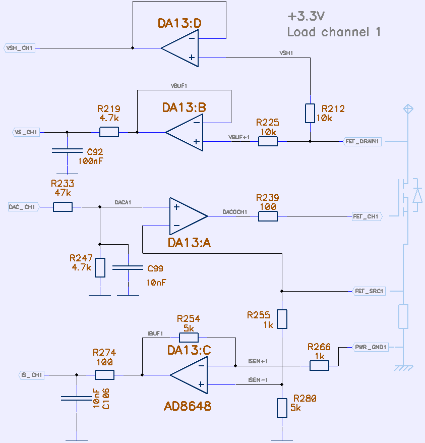
Image 1: MOSFET driver schematics, single-channel
DA13.A takes input voltage signal from DAC and drive power MOSFETs gate. DA13.C forms amplifier for current signal from low-resistance shunt, located right at FET pins. Shunt resistance is in range 10-20 mΩ to minimize power dissipated in shunt. Few standard 10W ceramic shunts in parallel connection are used.
DA13.B and DA13.D are just voltage follower buffers to sense input voltage at DC load and drive ADC inputs for measurements. Analog Devices AD8664 quadruple opamp used to allow driving long wires and high-power FETs with large capacitive gates. These opamps have low offset and unipolar +15VDC power, to allow safe margin on +12V input voltage operation.
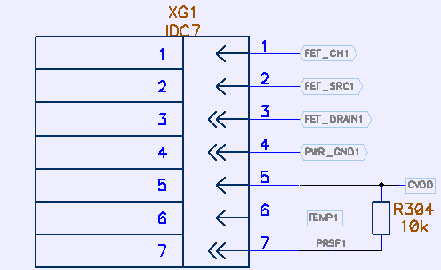
Image 2: MOSFET 7-pin connector
MOSFETs are physically located on isolated Intel Xeon processor heatsinks and connect with control board via dedicated 7-pin connectors. Since we don’t have very high performance requirements, this approach working okay. For better accuracy or higher frequency dynamic loads location of opamp much closer to MOSFET would be required to minimize inductance and capacitance of all signal nodes.
ISOTOP MOSFETs were really reliable at power levels about 350W and nice to use, but they are about $20USD each, so with 12 channels we need cost only on FETs alone would be ~$250 USD already. So I used pair of paralleled MOSFETs in TO-247 in the final design. I used paralleled pair of IRFP90N20D in TO-247 package to reduce cost, losing a bit of max power capability. Pair of IRFP90N20D was able to dissipate about 300W power with ambient temperature at +40°C, using Xeon 604 fansink with copper insert plate in base. Change of FETs to non-isolated TO-247 also rendered need of mounting heatsinks on Teflon standoffs, as they were under input voltage potential now, and we required separate channels to be isolated.
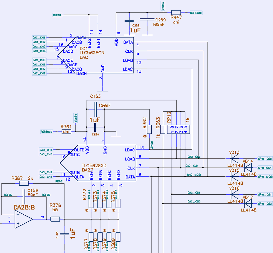
Image 3: DACs and SPI interface
Now, let’s take a look on DACs, which generate control signals to set current on each channel. Texas Instruments TLC5628 and TLC5620 were used. There 8-bit DACs can generate voltages up to +5VDC and have recommended load of 10 kΩ. Output settling time is just 10 µs with signal bandwidth at 100kHz. This is more than enough for our DC load application.
Reference voltage for both DACs, internal MCU’s ADC and external high-resolution ADC is taken from +2.500VDC REF192 zener IC.
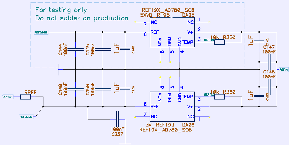
Image 4: Voltage references for DAC/ADCs
For testing and as option schematics and layout also implement +5.000VDC REF195. I was not sure which one will be better on schematic stage, so put both for a testing. In final design only +2.5V one was actually used. Analog Devices AD780 could be used for reference as well.
Analog Devices AD7490 16-channel 1MSPS ADC. It also have two 4051 MUX ICs for AC coupled measurement (such as voltage noise/ripple). Every high-voltage input divided by simple R2R and protected by Shottky diodes. Power decoupled close to chips by multiple capacitors of different size and value. This ADC have 12 bits of resolution, which in theory can provide us 0.0036V per LSB for +15V input range (with divider).
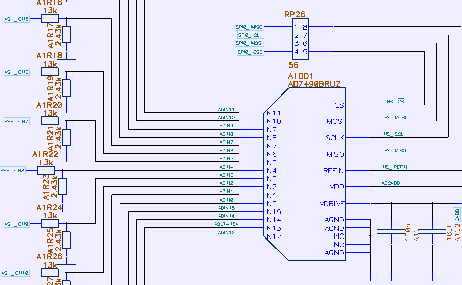
Image 5: High-speed multi-channel 12-bit ADC
There are two signal paths for measurement. MCU have its own internal ADC, which is used for measurement of current sense output and also have own R2R dividers to sense voltage sense. External ADC used only for high-resolution measurements, so actually it can be removed if less resolution and no AC measurements are acceptable.
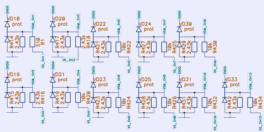
Image 6: Resistive voltage dividers for input voltage attenuation
Divider ratios are shown in Table 3 below.
| Input channel | Divider ratio | Nominal input range | Resistors |
|---|---|---|---|
| +3.3V | 0.618321 | 0 – 4 VDC | 1.5KΩ + 2.43KΩ |
| +5V | 0.340813 | 0 – 7 VDC | 4.7KΩ + 2.43KΩ |
| +5VSB | 0.340813 | 0 – 7 VDC | 4.7KΩ + 2.43KΩ |
| +12V (8 channels) | 0.157485 | 0 – 16 VDC | 13KΩ + 2.43KΩ |
Table 3: AD7490 input voltage divider ratios and resistors
Since we have 12 independent DC load channels, with both voltage and current on each, we end up with no less than 24 analog voltages which need to be converted to digital. Since we have only two ADCs (one in MCU and one external) external switching of signals was implemented with regular HEF4051 single-ended 8-channel multiplexors. Multiplexors powered with +15 and -5VDC rails, to accommodate full 0-15VDC input signal range.
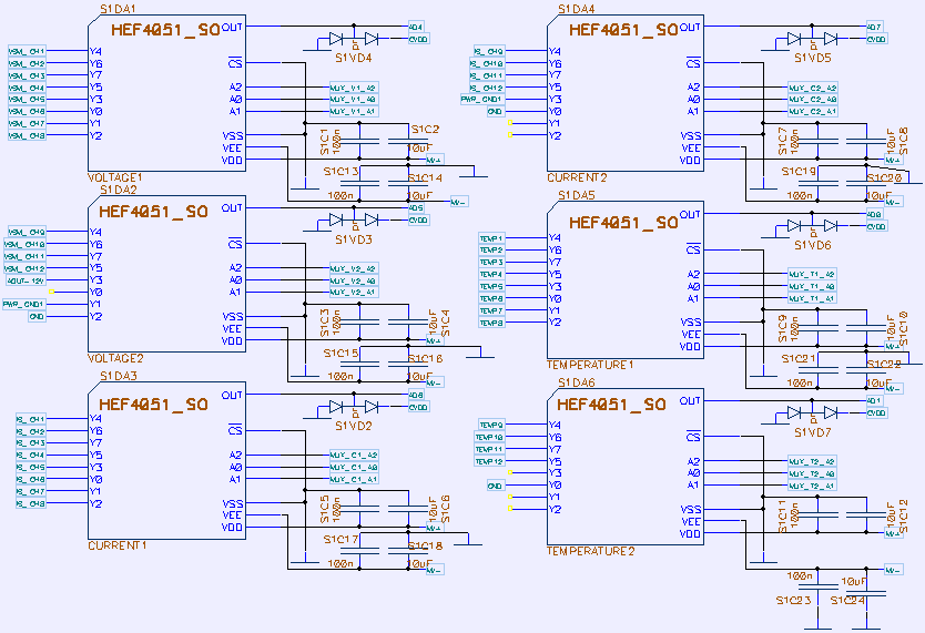
Image 7: Voltage/current channels multiplexing
To control digital signals at ATX PSU few TTL input/outputs were implemented. DUT and STBY are output for monitoring LEDs only, while PSON is signal to control state of power supply. These are terminated with standard 2.54mm 2-pin headers to connect with standard PC chassis buttons and LEDs.
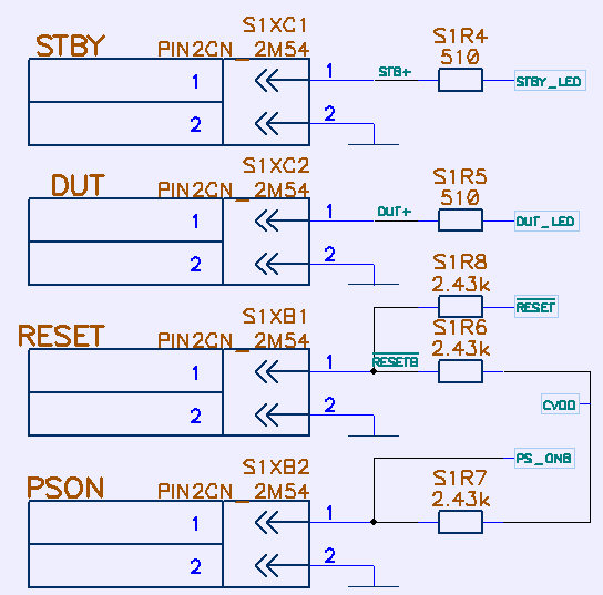
Image 8: Digital I/O and LEDs
Simple 2-way comparator circuit implemented with LM393 for easy user indication of passing/failing voltage levels on every connector/channel. LED is driven active when voltage is in 5% spec. Resistor network R9,R30,R42 at DA1:A and DA1:B inputs set comparator input voltages and are trimmed after assembly to feature correct ±5%-level thresholds on every rail voltage, like +3.3V, +5 and +12V. Just one shown here, but there are one per channel on board.
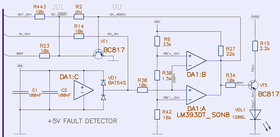
Image 9: Voltage limits and power health threshold monitors
All PSU input power connectors are to be located on same main PCB. Ports for voltage monitoring are also implemented to aid calibration with external test gear and noise measurement. Just one shown here, but there are one per channel on board.
Image 10: SMA debug ports
These can be used also as outputs to connect voltage signal to external oscilloscope, so more advanced measurements could be performed.
Image 11: Input load connectors
Input MiniFit-JR terminals are routed following standard ATX pinout, so usual connection with PSUs own cables could be easily and quickly done.
To control and monitor everything two digital chips were used, ATMEL AT91SAM7SE512 ARM7TDMI microcontroller with plenty of FLASH and RAM memory, and digital logic ALTERA MAX II CPLD was used for some glue logic and digital monitoring of connector states. Interfacing between ARM and CPLD is done via SPI. Selection of this microcontroller was made due to use in few other projects I had during that time, so using same series MCU saved some cost on debug toolkit, just as JTAG Debugger and software. In this application most of mid-level microcontrollers with ADC, Timers, SPI and interface such as UART,USB would does job just fine. My previous PSU ATE prototype was using AT91SAM7A3 (that MCU is based on same core, but features two ADCs, with total 16 input channels)
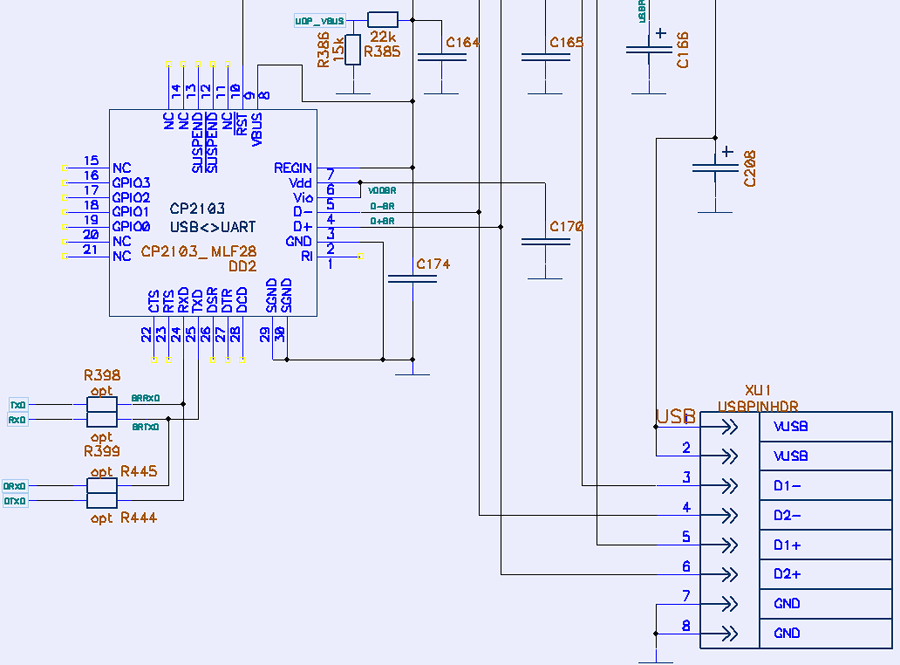
Image 12: CP2103 UART-USB bridge interface
Interfacing with host computer is implemented via UART-USB bridge, Silicon Labs CP2103. Why bridge? Since my major is not software, I opted to use simple UART in firmware programming instead of USB, which would need more work and may need time consuming debugging. I’d rather dedicate more focus on analog/hardware design for this project instead.
Now after we finish all main schematic domains complete, we can define and design local power supply regulators:
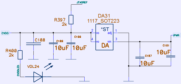
Image 13: Digital +3.3V power LDO
Digital power is simple +3.3VDC 1117 LDO, with MLCC capacitors on both inputs and output.
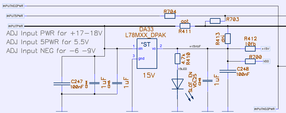
Image 14: Positive power LDOs
Main input power is L78M15 DPAK-sized +15VDC LDO, which takes unregulated +18VDC input. There is no input protection implemented, as this is supposed to be hardwired permanently to ATE’s power supply, and not managed by user in any way.
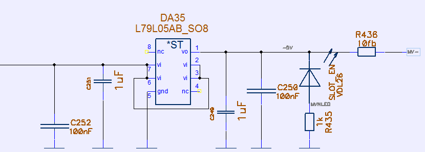
Image 15: Negative power LDO
Negative -5VDC is generated from ATE’s -12V PSU via simple L79L05 LDO. All power voltage monitored by LED to allow quick glance on power presence. As you can see, all regulators are linear, as power consumption of all measurement and control circuitry is small. Also linear regulators are less noisy than switching-mode ones, so it would help to avoid issues with noise and interference with analog signals in design.
Full schematics of everything can be downloaded from link below
xDevs.com Neutron, PDF-format full schematics
xDevs.com Neutron, PCAD 2006 format SCH file
Layout design
Layout of board should always take actual location, placement and connectors interfaces into account during design stage. Initial sketch of board with components was printed on paper and located into actual chassis to see if dimensions, placement of connectors and cabling is suitable. Think about how board will be mounted, how it will be cooled if high power parts are present, and does it need to have user accessible parts and ports.
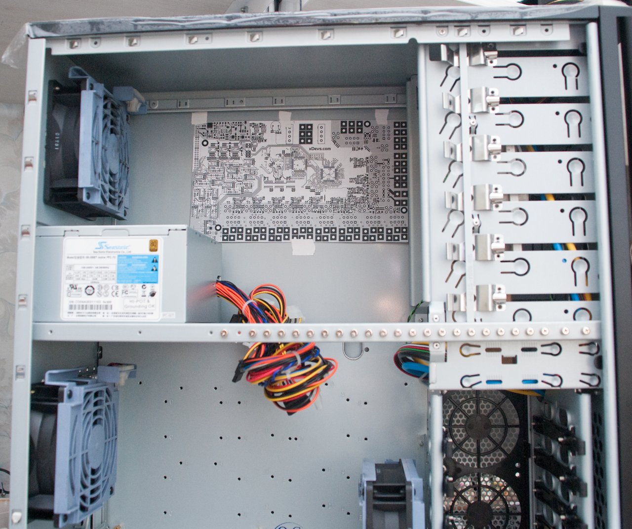
Image 16: Estimated board location and size
Prior to any routing first step is placement. At this step components are created with proper footprints and dimensions and located in functional groups together. Then groups are placed on board outline, with respect of overall engineering rules for mixed-signal environment. Try to group analog signals in single area, while digital domain is located separately. In our case placement domains are grouped as:
- Local power regulators, top left corner near power interface connector
- 12 MOSFET channel/sensing ports are located middle left side
- Opamps and DACs located right near channel connector
- +12V PCIe connectors are grouped on bottom of PCB
- System, CPU connectors are located at right edge of PCB
- ADC and references on top middle area, near edge
- Digital control and ARM+CPLD located in center
PCB is designed in four layers, with inner layers dedicated to power and ground copper fills. Let’s take a look on few PCB areas more closely.
All power grounds are separated from logic/digital grounds to prevent high currents flowing thru small-signal chips, causing potential measurement errors.
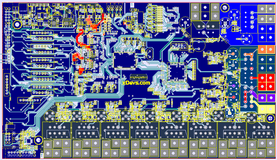
Image 17: Top side with routing and silk-screen
Most of passives are used in 0603 size, which are still not hard to assembly manually with soldering iron, while saving lot of space for routing. IC packages are SOICs or TQFPs. Only pin-less package is CP2103 QFN, which is easy to mount on using common industrial heatgun.
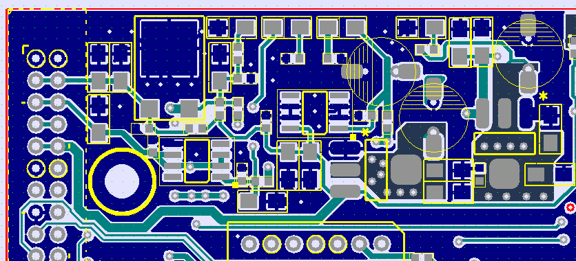
Image 18: Layout for local regulation circuits
All LDOs grouped together, with few electrolytic capacitors and indicator LEDs. They are physically located near input power connector, and provide power to all circuitry via wide traces or inner plane shapes.

Image 19: Digital ARM+CPLD routing
Digital signals are grouped together per function and routed together. Most of decoupling capacitors are located on bottom side right under chip. This is not best way, so I used extra capacitors to help with overall ESR/ESL of decoupling networks. Best is to have decoupling on same layer with digital chip, within few hundred mils away max.
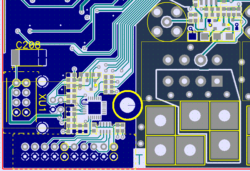
Image 20: USB port location and routing
USB and JTAG debug power located on bottom left corner of PCB. USB connector is colayout with either 2×4 2.544mm pin header, compatible with usual PC MB USB brackets, and with USB Type-B footprint for standalone use without chassis.
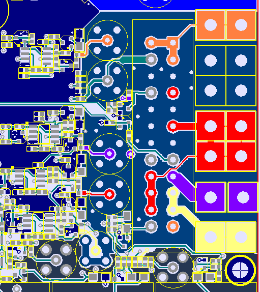
Image 21: ATX input connector and test ports
SMA test ports are located right near MiniFit-JR connectors and routed by wide trace on inner layers to minimize DC voltage drop. SMA ports support both high-impedance and 50Ω test gear loads.
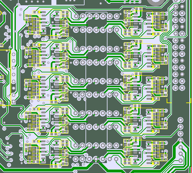
Image 22: Bottom side DC loads analog amplifiers
All analog amplifier circuits, shown on schematics Image 1 are located right at 7-pin header ports on bottom side of PCB.
Here’s result on all four layers:
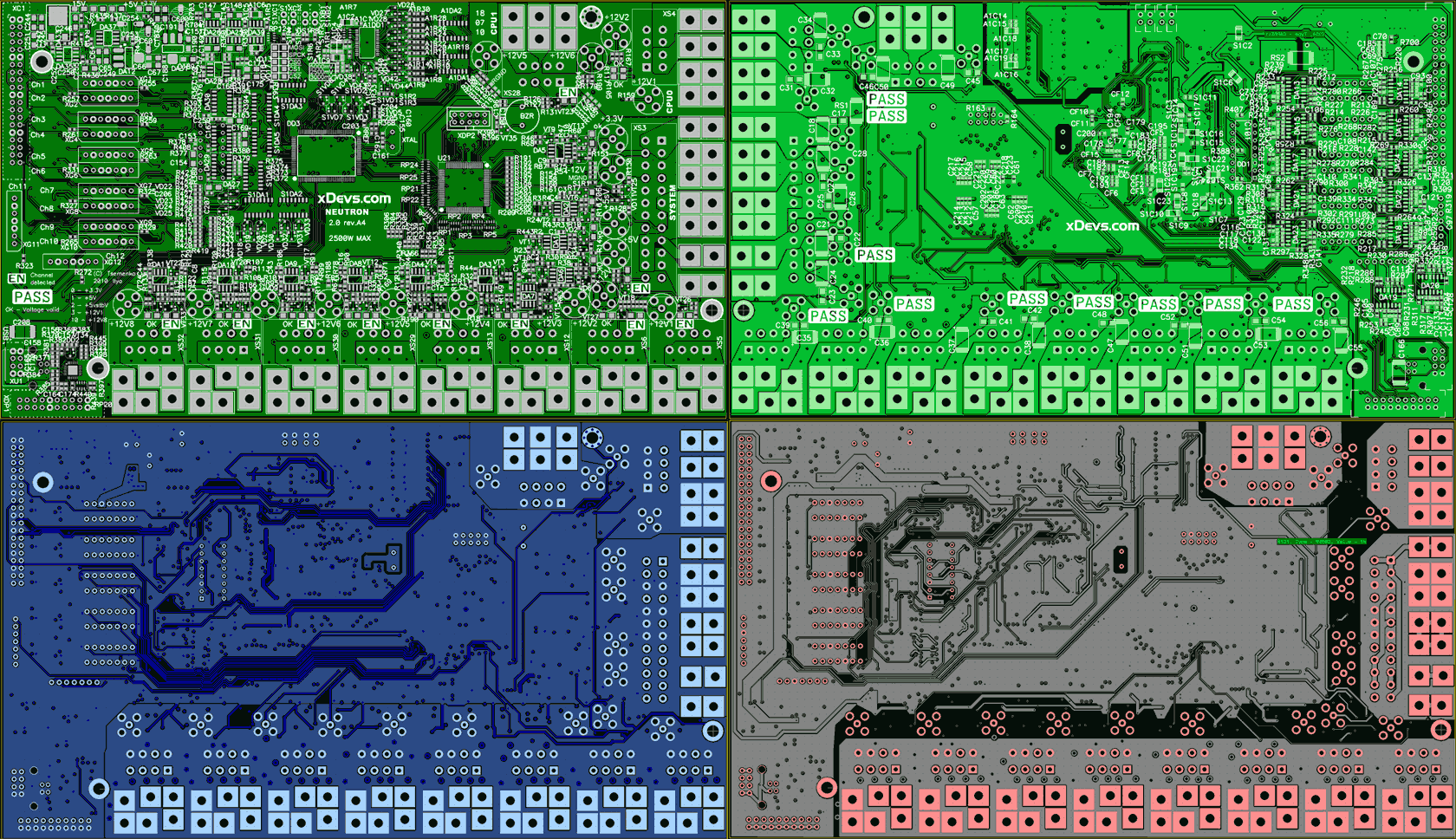
Image 23: Overall view on all four layers
As you probably already guess, here are main key features on PCB:
- Rectangle chip – 32bit CPU with 32KB ram, 512KB Flash
- Square chip on right side of CPU – ALTERA programmable logic, it monitoring each output state, presence of channels, connectors etc.
- Big edge holes – is where power wires go to electronic loads.
- Chips on left and left-center side – analog switches and DACs for controlling load.
- Bottom left edge – dual USB interface and debug port
- Top left edge – power supply (+3.3, +15, +12 -5 volts)
- Top center – 16ch high-speed 12-bit ADC for noise and precise measurements.
Layout was routed fully manually in ACCEL PCAD-2006 in a less than 2 weeks (with 5 revisions).
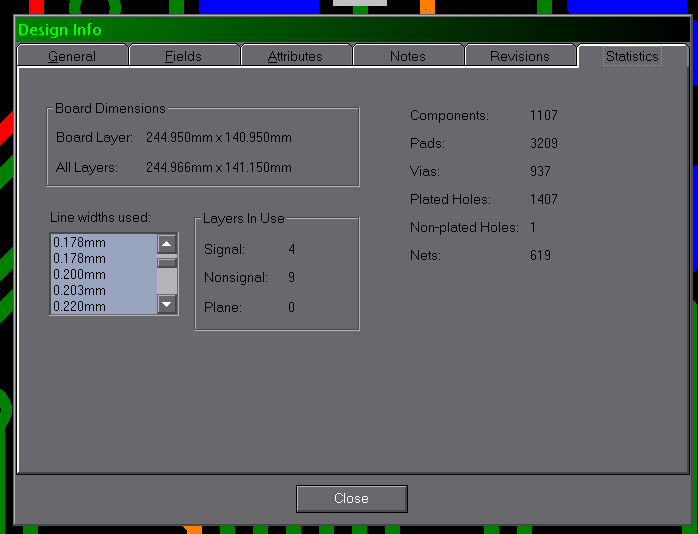
Image 24: Layout stats
3D CAD with components locations to check if any packages interfere with each other.
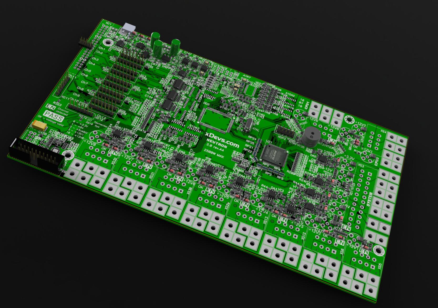
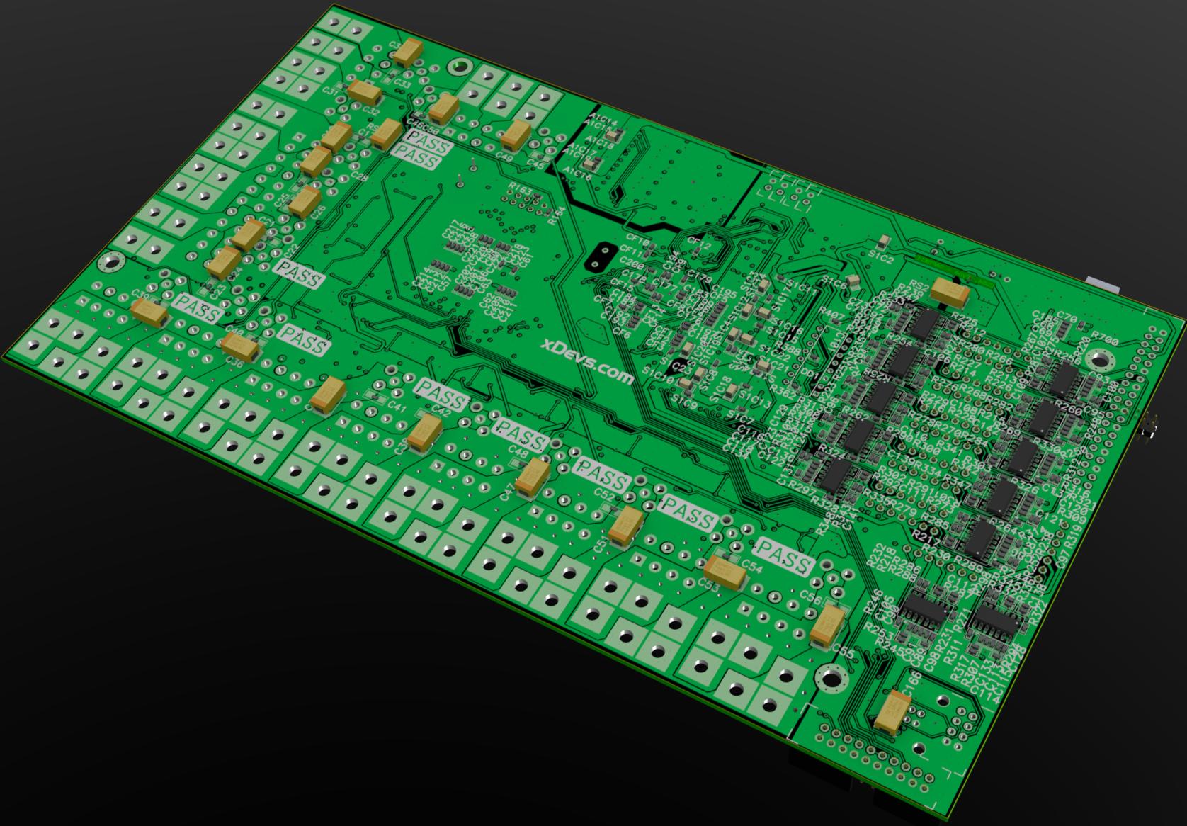
Image 25&26: 3D rendering of PCB with some components
2pcs PCB were ordered at local Ukrainian manufacturer, Galvanotechnika , and after about a month received. Cost of each PCB was ~$120 USD.


Image 27,28,29,30: Actual manufactured 4L FR4 PCBs
PCB quality is very good, no issues found.
xDevs.com Neutron, PDF-format, top assembly layout
xDevs.com Neutron, PCAD 2006 format PCB file
Unit assembly
It’s time to solder those one thousand one hundred seven components on both sides of board manually just by two solder irons (most of parts are 0603 resistors and capacitors of different values). That took about 30 hours to complete. Why two irons? One was small 25W, ERSA MultiTip C25 with 1.2 cone tip, to solder small components and passives. Second iron, high power 80W-type was used to solder all power connectors and thick AWG16 wires.
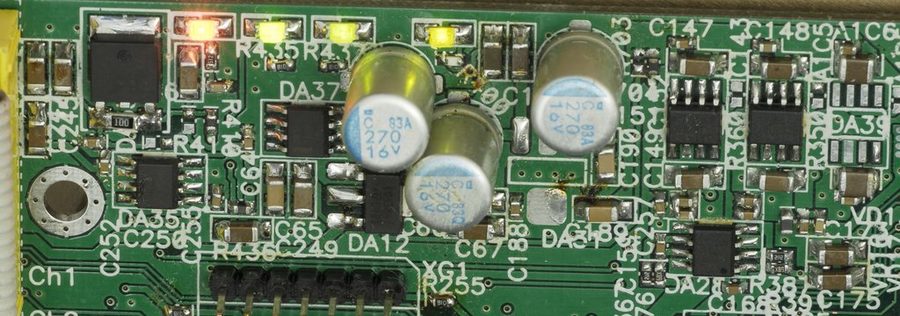
Image 31: Local LDO’s and references assembly
First step would be onboard power regulators assembly and test. You don’t want to solder all big TQFP packages just to blow everything up if that onboard power supply had wrong output voltage. After getting all main voltages in spec, we can also test them with rated currents to make sure they work reliably and within specifications. Then we can follow with onboard analog voltage references.
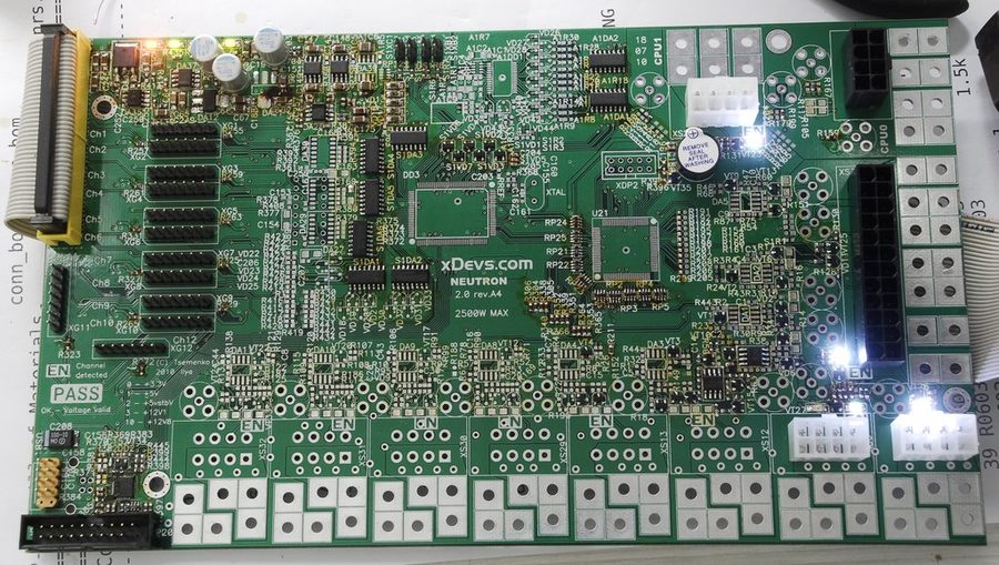
Image 32: First day assembly result
After power working and tested well, analog front end parts to be assembled and few connectors to allow connection of test signals. Correct multiplexer operation as well as voltage levels after voltage dividers to be tested at this point.
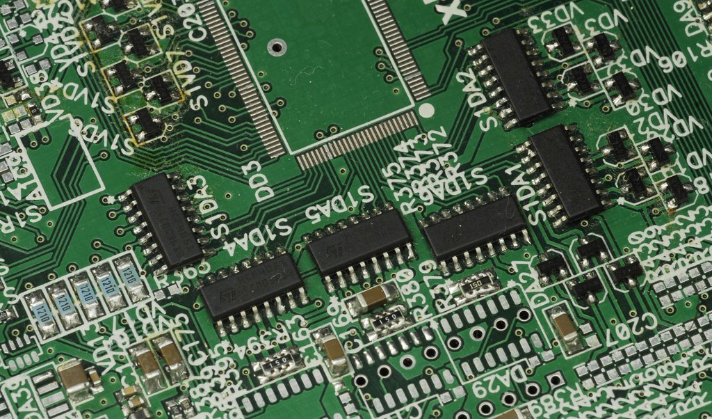
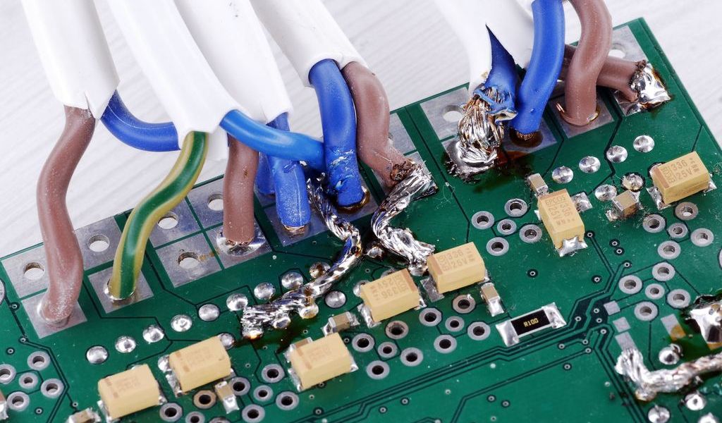
Image 33,34: Input analog MUX section and input power cables
Now standalone circuits such as USB bridge and level detection comparators can be populated.
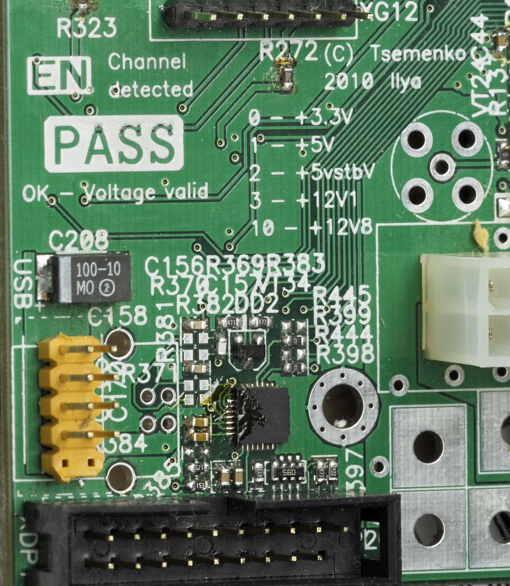

Image 35,36: USB Bridge and LM393-based comparators
Also I made some errors with PCB routing, 5 lines was not proper voltage level. So needed to cut traces and insert NPNs.
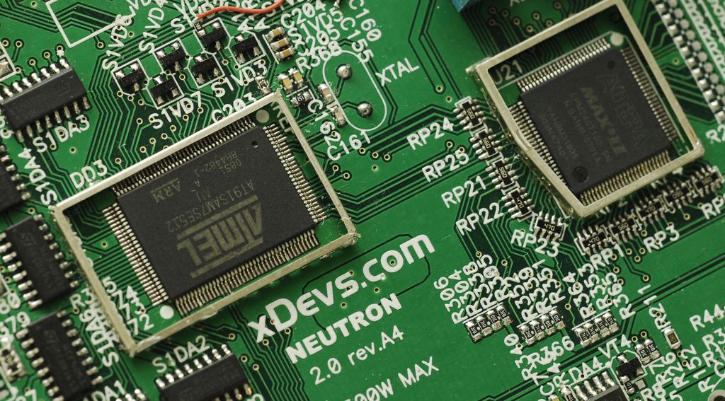
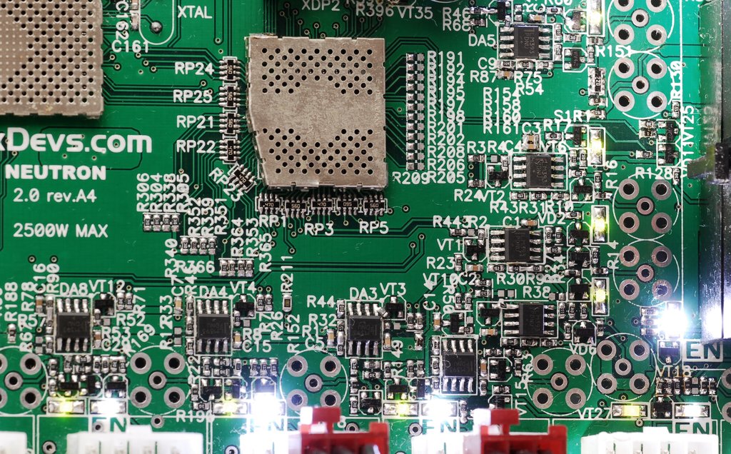
Image 37,38: ARM7TDMI MCU and ALTERA CPLD
Now we can check if digital brains are alive and can reply with ID requests
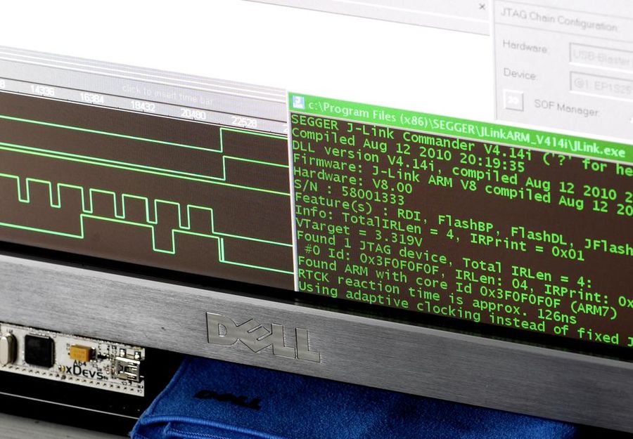
Image 39: Detection successful using SEGGER J-Link interface to ATMEL ARM
No problems here, CPLD also replied correct ID to USB Blaster and ready to accept bitstream.
We can put on DAC/ADCs and get ready to start firmware/software development.
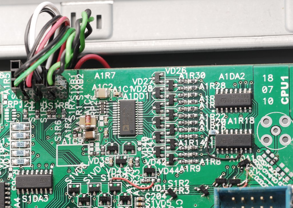
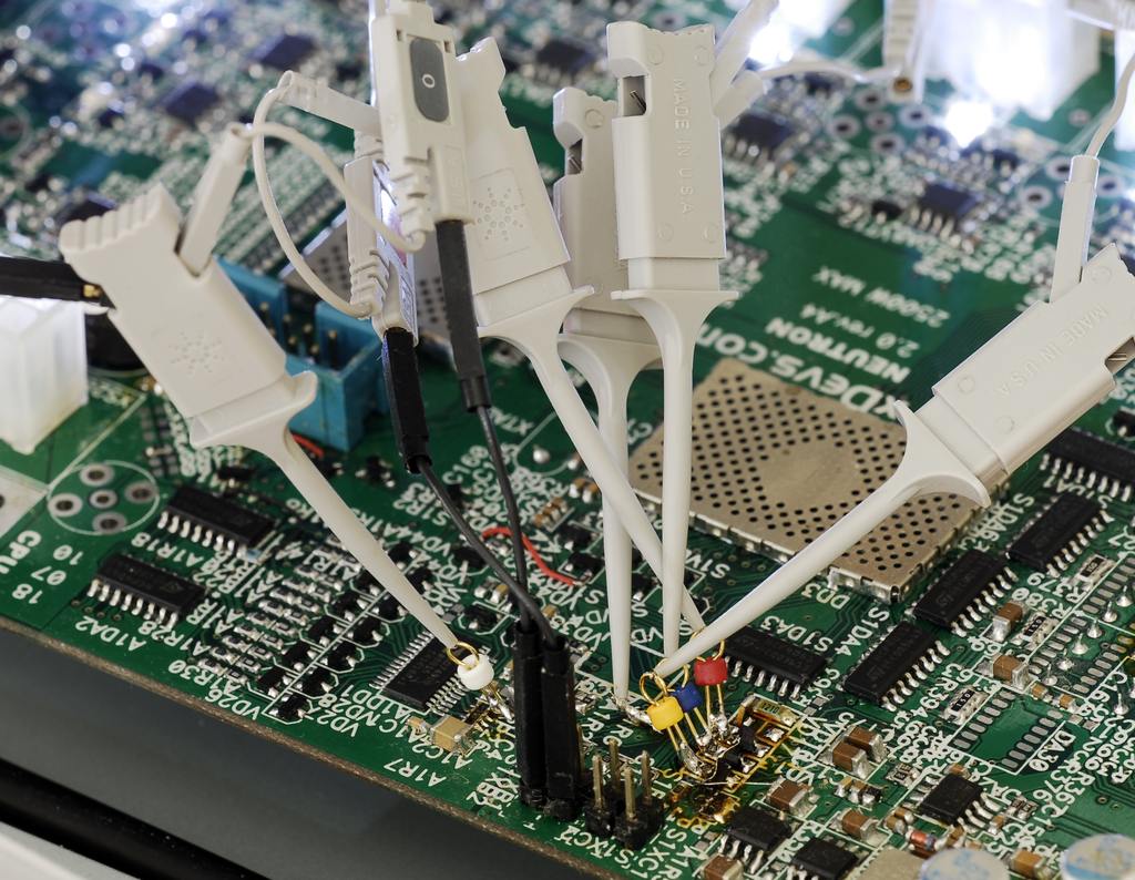
Image 40,41: AD7490 external ADC and SPI interface probe hooks
For initial debug and testing I was using jellybean LM324 opamps, so photos I had are with these cheap generic parts. Later I had issues with oscillation on very top end power levels, so replacement opamps to pin-compatible Analog Devices AD8648 fixed stability issues.
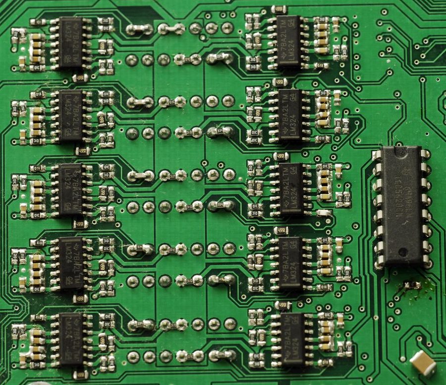
Image 42: MOSFET channels operational amplifiers
Also, put attention to polarity of capacitors during soldering. For example I mechanically soldered this tantalum on board, without checking polarity of signal, which was negative -12V rail. Resulting fireworks were well expected:
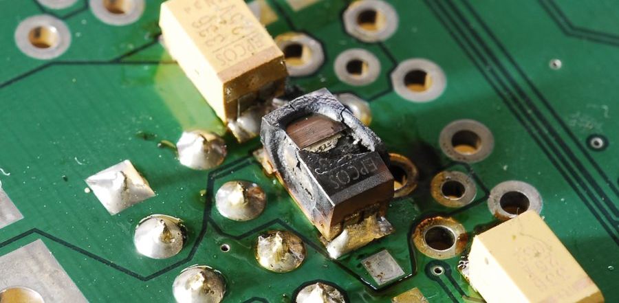
Image 43: Do not solder polar capacitors in wrong polarity!
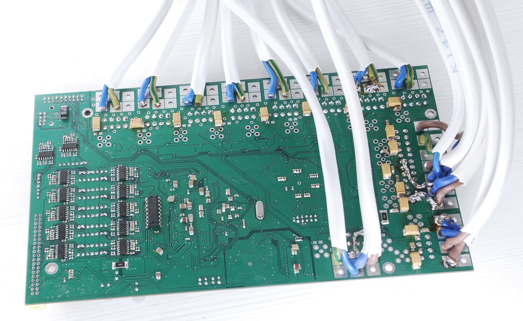
Image 44: Assembled board with cables ready for installation into chassis
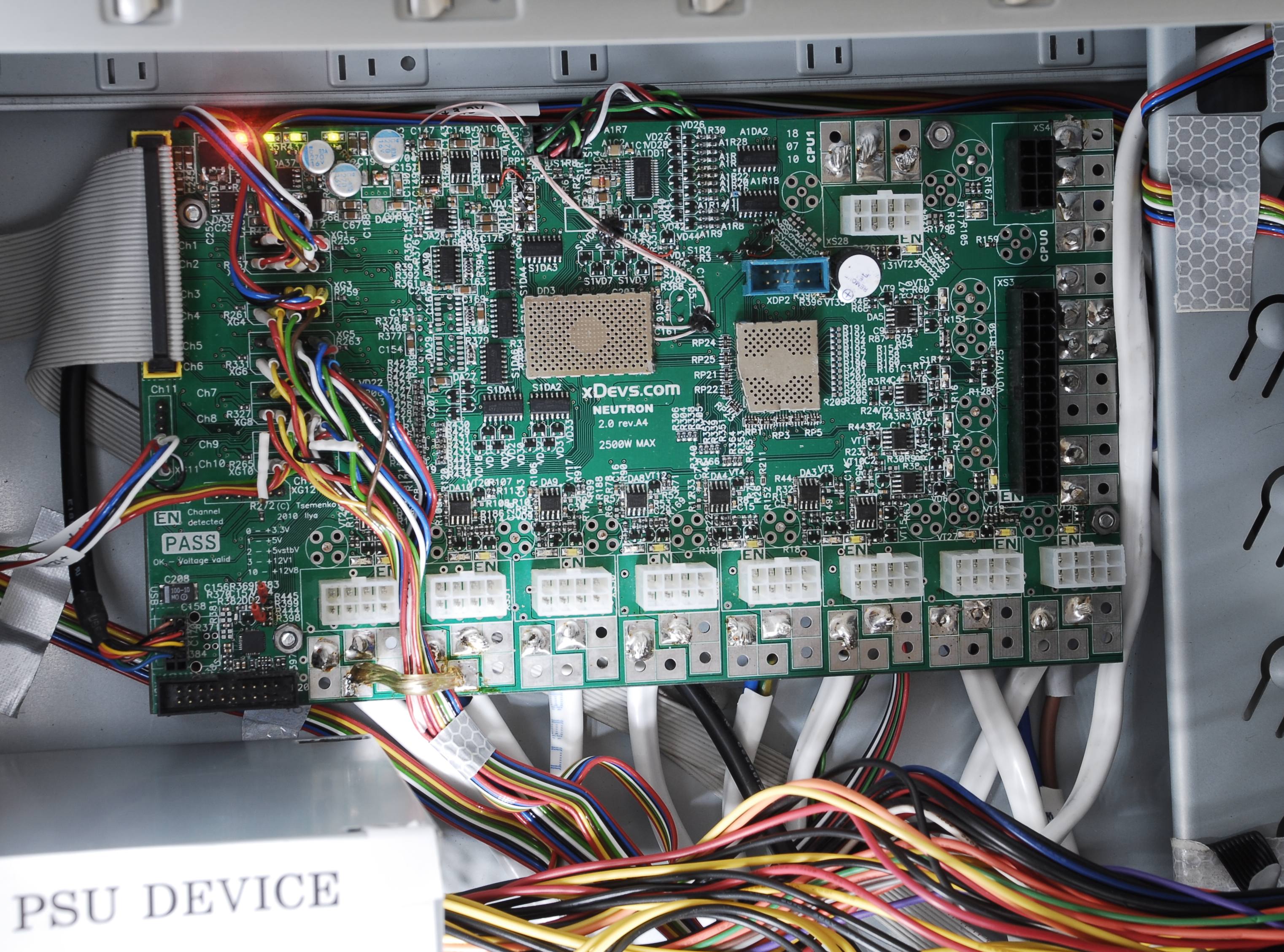
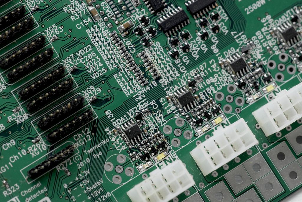
Image 45,46: Board installed for development and input monitors channels!
Now few words regarding actual external DC loads construction.
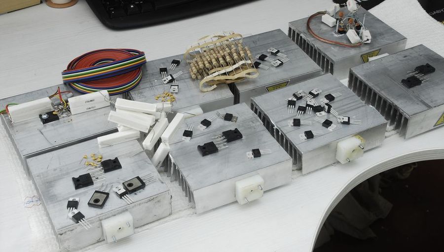
Image 47: MOSFET blocks and heatsinks
I tried few mounting and wiring approaches. TO220 IRF3205S FETs were not able to handle required power levels during constant long-time operation due to thermals. They are good for ~120-140W loads, but anything over that is running system at edge. Usual failure mode is short in die and excessive current draw from input PSU.
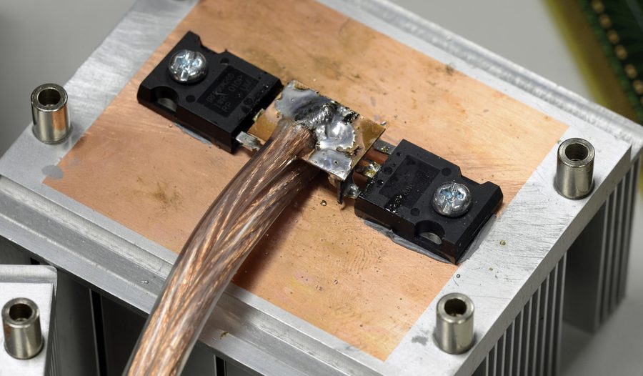
Image 48: Revision on power load
Improved version has two TO-247 FETs located symmetrically on heatsink. Input power is routed to both of them with copper plate for easier soldering and assembly. Gate and voltage sense signals routed back to control mainboard using thin coax wire in final variant.
 !
!  !
!
Image 49,50: Loads installed in case
All heatsinks are mounted on Teflon blocks, fully isolated from chassis frame.
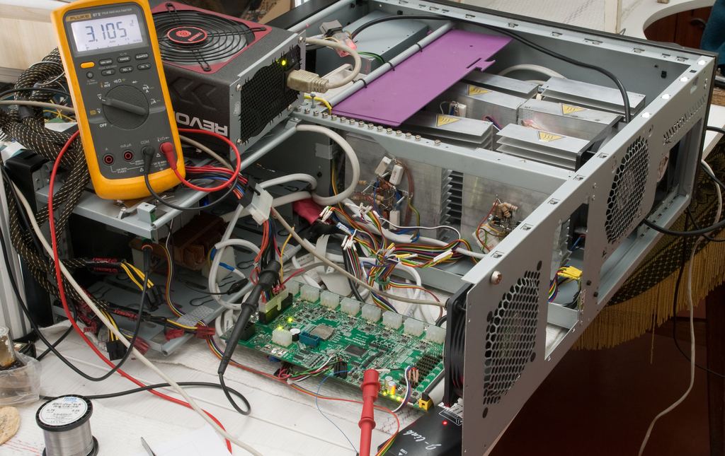
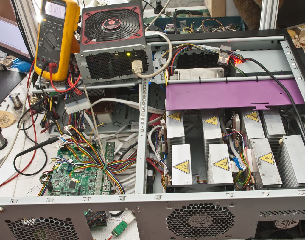
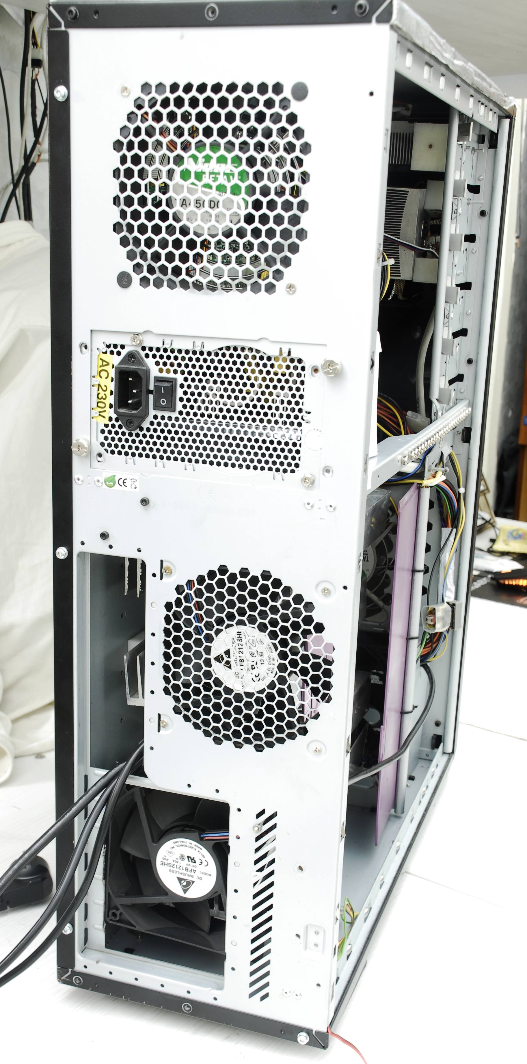
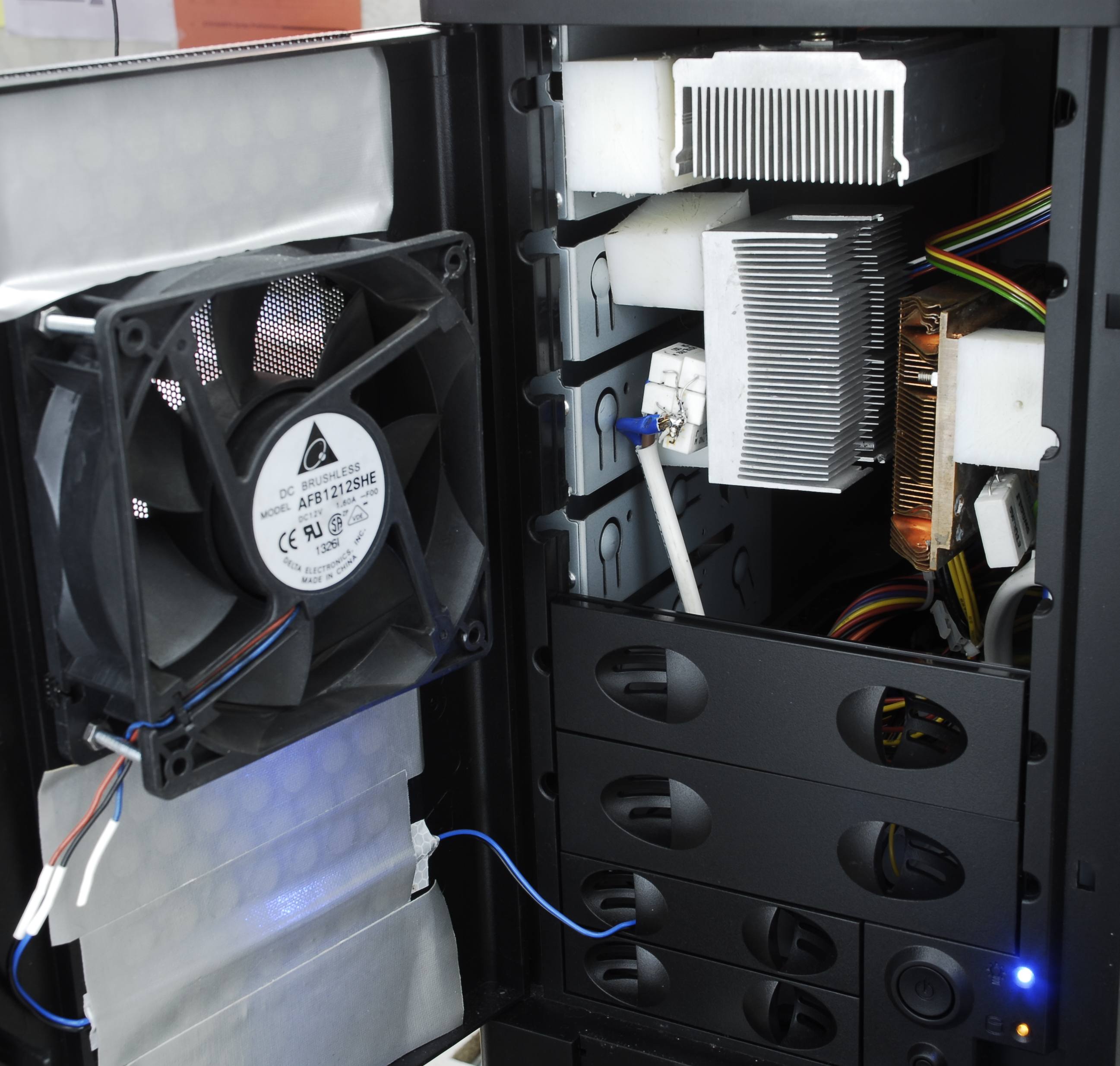
As DC load units getting loaded, their temperature will quickly raise. If we don’t take care of thermals and proper airflow MOSFETs will quickly reach critical temperature and fail. To avoid this catastrophic failure, forced air-cooling is a must. I used six high-power server 120×38mm +12V fans to push air thru chassis.
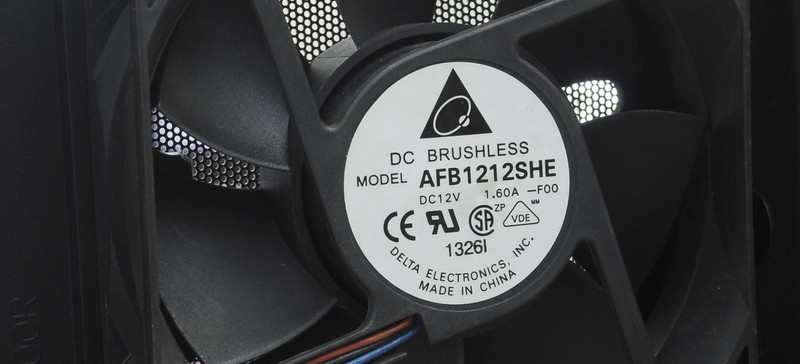
Image 51: High power DELTA fan
Drawback of this approach is high noise levels. So we want later to minimize test runtime to avoid long periods of generated noise from test system.
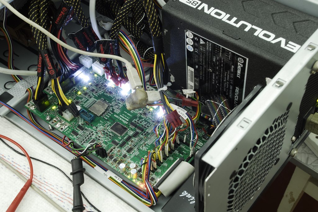
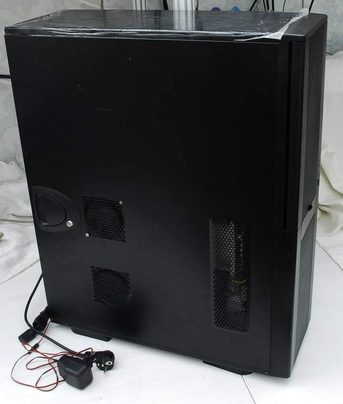
Image 52: ATE board in chassis
 !
! 
 !
!
Image 53,54,55: Test system in chassis
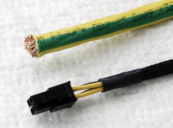
Ground returns from DC load modules to PSU were handled by thick AWG12 wire. To give comparison of wire gauge used:
I also had another assembly version, more suitable for production line testing, using rackmount 4U chassis. Here’s prior assembly construction, allow to see used heatsinks and overall placement.
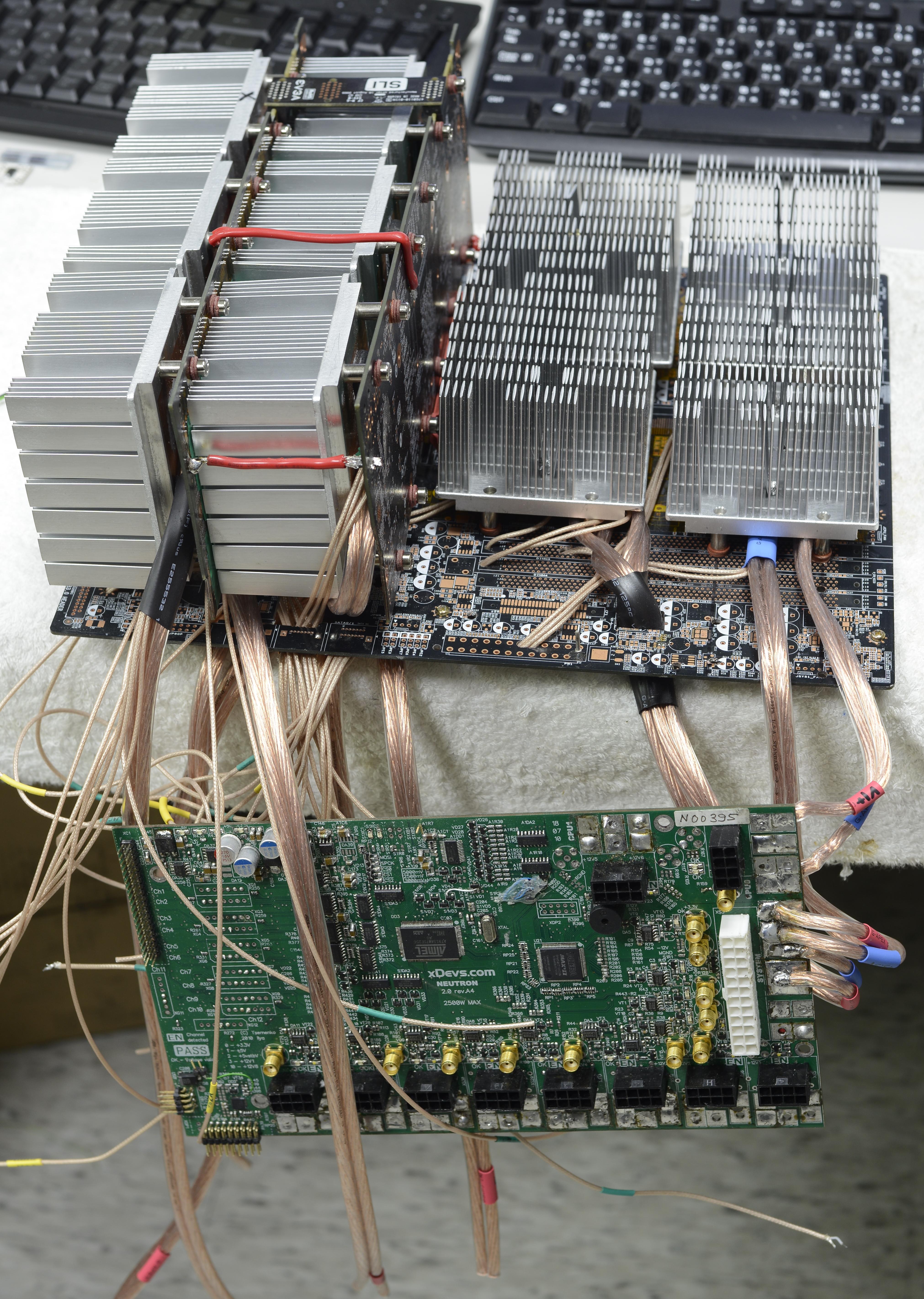
It features same board and hardware, with DC loads mounted on dummy motherboard PCB. “VGA” DC loads are mounted on PCI-express dummy PCBs, with three channels on each.
HDL design
Simple digital SPI core was used to interface with MCU. CPLD is used as future-proof automatic testing and timing measurement device, and real-time monitor for voltage threshold crossing. Since it runs separately, main microcontroller doesn’t have to worry about pooling and I/O handing and can check status only when IRQ signal from CPLD is toggled.
ALTERA MAX II EPM240T100C5N POF bitstream
Firmware design
Neutron ATE system firmware is developed in-house, using ARM C compiler and IDE. There are about 10K lines of C code involved. This took me about 5 month to develop, debug and test.
AT91SAM7SE512 MCU firmware binary, V1.0.0.421
Communication with software side is done via simple ASCII-command protocol, as listed in tables below. Base command syntax parsed as:
!XXX;VAL.VAL;/.../;#
- ! – is command identifier symbol,
- XXX – command name
- ; – separator
- VAL.VAL – value, eg 12.416
- ;# – end separator
Command reference
| Command | Function |
|---|---|
| !!! | Host link request for report; return !REP command |
| !SC;%02d;%05d;# | Set current command in manual mode; return channel,current in mA; |
| !TRO;%02d;%05d;%05d;# | Enable transient test; return channel, current in mA, time in ms; |
| !TRF;%02d;# | Disable transient test; return channel |
| !STR;%02d;%04d;%04d;# | Writes to config reg yy, value zzzz.xxxx; |
| !SLC;%03d;# | Set +3.3/+5V loading ratio (0 to 100% towards +5V) |
| !GV;# | Request for channel data values; |
| !GHV;# | Request for high voltage data; |
| !EF;%02d;# | Start efficiency test (with xx% step) |
| !ATS;%03d;%04d;%04d;%02d;%02d;%03d;# | Start khx test, low_pwr_val, hi_power_val, total_pwr_val, rails12v, dut_type, steps;# |
| !PN;# | Power on DUT via PSON |
| !PF;# | Power off DUT via PSON |
| !FAMC;%03d;%04d;%04d;%03d;%02d;%02d;# | Start linear test, same as ATS format |
| !STS;%02d;%03d;# | Standby autotest, xx – power in W, yyy – steps |
| !NTS;same as ATS;# | Noise autotest, values same as ATS format |
Table reference: Commands from software to ATE, requests
| Response | Function |
|---|---|
| !REP;(str);# | Hello string with device info |
| !TN;%05d;# | DUT powered on by measured time x |
| !TF;%05d;# | DUT powered off by measured time x |
| !ERR;%02x;# | Error occur, with number a |
| !FAN;%05d;%05d;# | Fan rotating speed x,y; |
| !VC;%02d;%02.04f;%02.04f;%03d;%03d;# | Values from channel a, x.x – voltage, y.y – current, nnn – noise, f – nfreq; |
| !MT;%03.01f;%03.01f;%03.01f;%03.01f;# | Temperature on sensors (x,y,z,a) in 123.4 format. |
| !ATE;# | KHX test done |
| !AT;# | KHX test started |
| !G;%05d;%02.04f;%02.04f;…all channels…;# | Dot data #xxxxx for KHX graph. |
| !S;%05d;%01.04f;%02.04f;# | Stanbdy data, a.a – volts, bb.b current; |
| !N;%05d;%03d;…all channels…;# | Data from noise test, aaa – per channel noise lvl |
| !ST;# | Standby test started |
| !STE;# | Standby test end |
| !NTS;# | Standby test started |
| !NTE;# | Standby test end |
| !FAMS;# | Fan/efc test start |
| !FAM;%03d;%03d;%03.01d;%03.01d;%05d;%05d;# | eff/pf/temp graph data, effc (100 mean 1.00 on graph); pf;temp1;temp2;fan1;fan2;# |
| !FAE;# | Fan/effc test end |
Table reference: Commands from ATE to software, responses
As example command to adjust DC load current to channel 5 at to +25.415 ADC will be !SC;5;25415;#
Software design
Friend of mine, software engineer helped with simple, yet functional Windows-based control software tool, to control all channels and perform automatic tests.
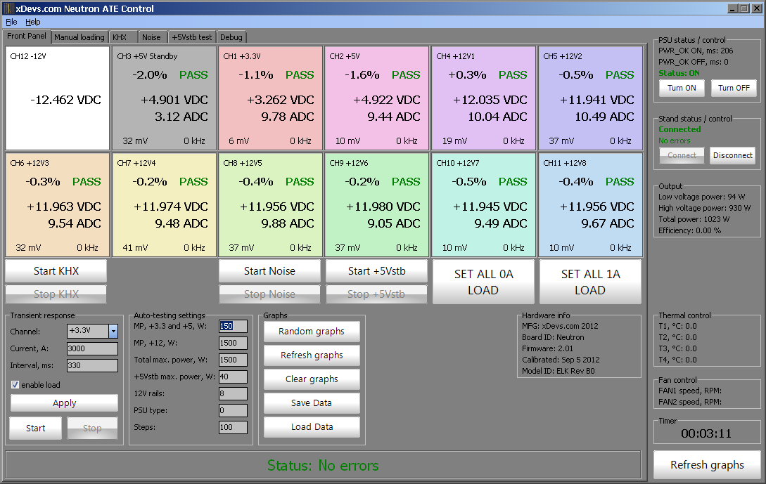
All channels fully independent and can be adjusted at any time in manual mode. This allows to apply any combination of constant load current for longterm PSU testing. Monitoring of input voltages and currents is continuous in realtime, to allow quick evaluation of each channel.
Manual mode allows adjustment and simultaneous measurement on all channels, using simple sliders in GUI
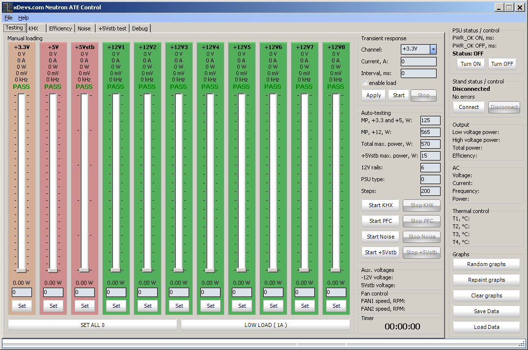
Software have ability to set all key controls and customize graph views.
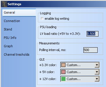
Loading balance between +5V and +3.3V rails is set by ratio LV load ratio, with acceptable values from 0.0 (all load at +5V) to 1.0 (all load to +3.3V). Default is to keep both rails same 50% power, with 0.5 value.
Polling interval sets measurement frequency time, and log writing stores all received/sent commands in text log for debug purposes.
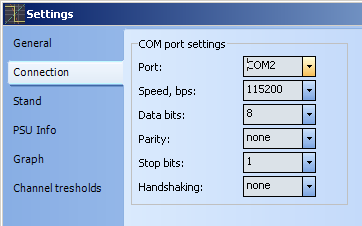
Serial interface settings are fully adjustable, but should not be changed normally.
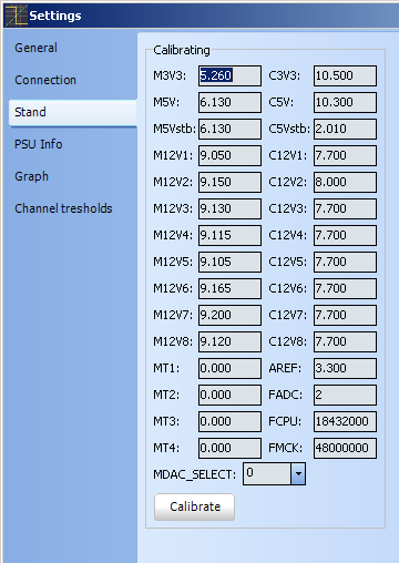
Calibration coefficienct are provided for finetuning ATE performance.
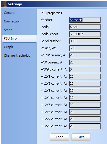
Most common used setting tab, with PSU information allow user to set manufacturer information, such as brand, model, serial number, rated power limit, as well as specific current limits on each rail.
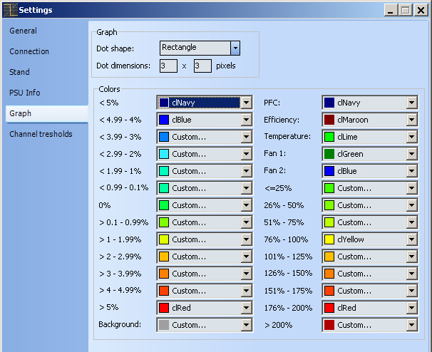
Graph settings include controls for color settings to each deviation level and graph pixel size.
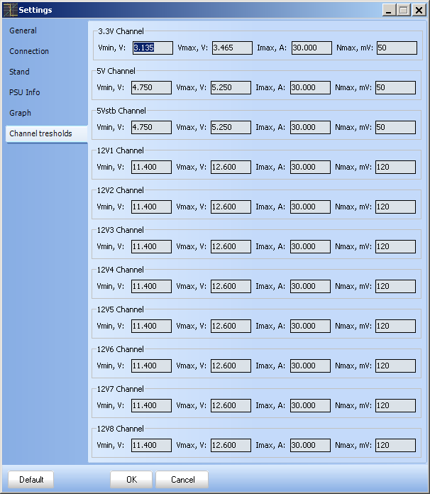
Thresholds setting are controls for PASS/FAIL limit indicators, each rail separately.
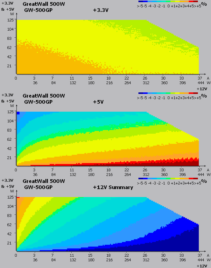
In automatic test operation ATE firmware run DC load sweeps from zero power at +12V to maximum defined load. Measurements for all voltages and currents are taken on every loading point, resulting automatic rendering of graphs for every channel. These graphs allow easy and fast evaluation of voltage regulation performance, on each specific loading crosspoint. X axis shows total loaded power on high-power +12VDC channels, while Y axis used for total loaded power for +3.3V and +5V channel, combined. Every point on graph shows combined total power on PSU. Each signle graph shows voltage deviation from specification (with +3.300V, +5.000 or +12.00 VDC as 0% deviation, ideal level). For easy understanding each 1% gradation is colored with own color, till voltage goes off limits -5% or +5%. Use green color for 0%, blue color for lower voltage, red color for higher voltages makes evaluation of PSU performance regulation very easy – more green – better regulation, more red or blue – bad regulation.
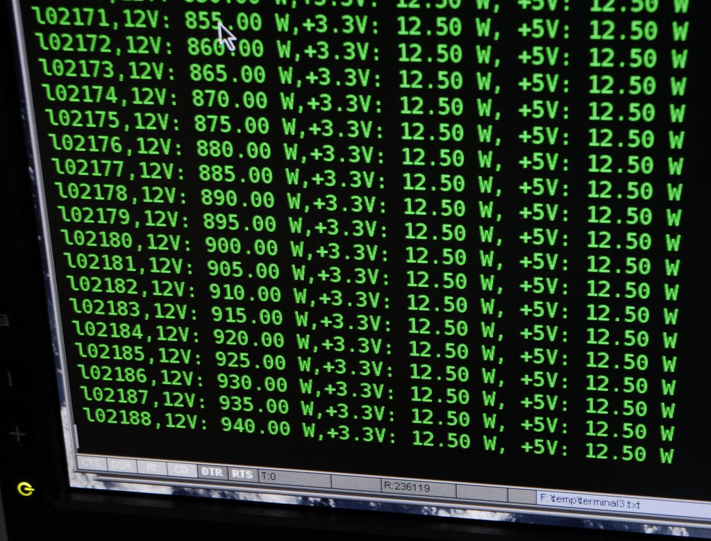
User can set any border limits for loadings and distribution, limited only by ATE capacity at about 2000W. Amount of +12V channels used is automatically detected by ATE firmware during test start and setup, and current steps are automatically calculated, with usual range of 200-500 mADC per point. Typical 500W PSU test in this automatic mode takes about 30 minutes, with more than 10000 measurements taken per each channel. It would not be viable to perform such comprehensive test manually by adjusting DC load and writing down measurement results.
xDevs.com Neutron software tool, executable
Calibration and adjustments
Measured accuracy with separate 20ADC current shunt and Fluke 87V 4½-digit DMM revealed <3% error on low current settings below 4.0 ADC and accuracy about 1% for main operation range 4-20ADC.
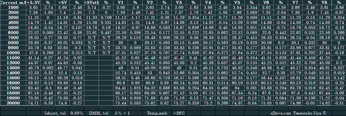
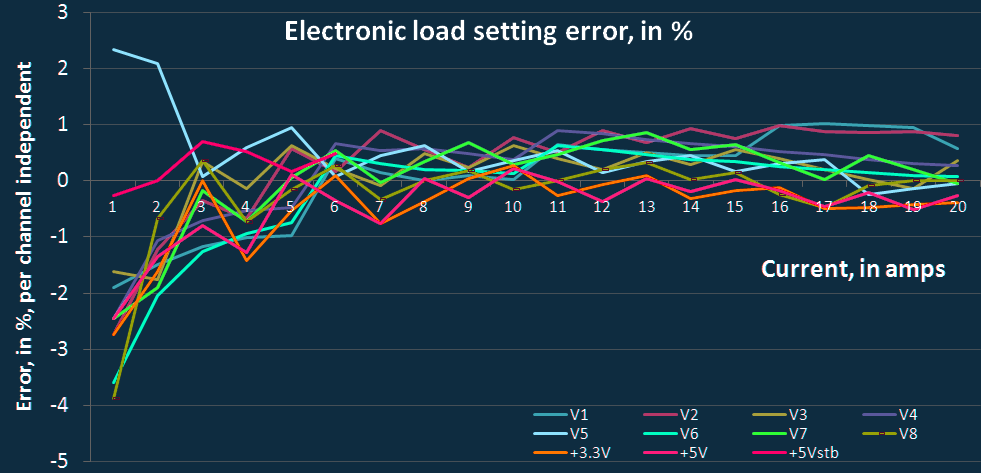
Same data, but on graph display.
xDevs.com Neutron analog front end was calibrated using next instrumentation:
Calibrated 4½-digit DMM Fluke 87V
100MHz oscilloscope Tektronix 2246-1Y
Calibrated thermometer Fluke 51 II
FPGA Signal generator/analyzer based on Parallax SmartPack 672
Performance and test examples
Let’s try very good high-end PC power supply, Enermax ERV1050EWT (1050W power capacity) with next test settings, 150W for low voltage rails combined, 580W for +12V, 680W total power limit.
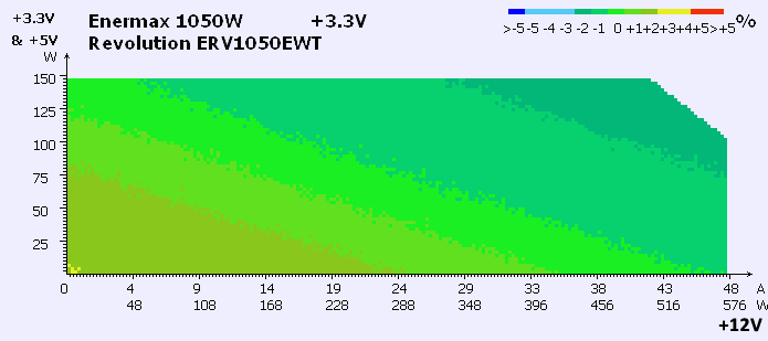
All main channels well within 2%, with Standby barely hitting 3% at low loads. Overall graph understanding this is easy, more greenish – better. Color is showing how much output voltage deviate from ideal level. ATX standard require PSU to meet 5% max deviation with any possible load configuration.
Now let’s test bad cheap ATX power supply.
Here we can see that while +3.3V channel is not so bad, stays within 3% tolerance at all times, we can’t say anything good about +5V and main +12V channels. +5V goes over allowed +5% on low loads, and at same time +12V goes way below required -5% for 444W loading scenarios.
Looking at this graphs is it not hard to understand now, why taking DMM and just measuring power supply voltage in static operation mode does not mean PSU is good or bad. Single measurement is only a single dot on graph, at given loading condition point, while in reality computers power demands are dynamic and vary a lot, depending on what computer actually doing. If it’s just sitting in desktop, while user just barely does anything (like typing this article in notepad), CPU and GPUs are barely working, mostly staying in idle state. That would be bottom left side of graph scenario. If PC is running some math program, such as calculating SPICE simulation in our favorite electronics simulator – CPU will be loaded, taking hundred watts from +12V. If we have modern gaming system with pair of high-end PCIe graphic cards playing game in 4K resolution, we likely to find our consumption right at top right high-power corner of graph.
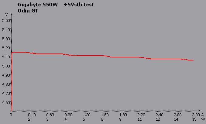
Stand-by test is performed with power supply in stand-by mode, with main rails OFF. It’s simple I-V curve with loading ramp from no load to max specified loading:
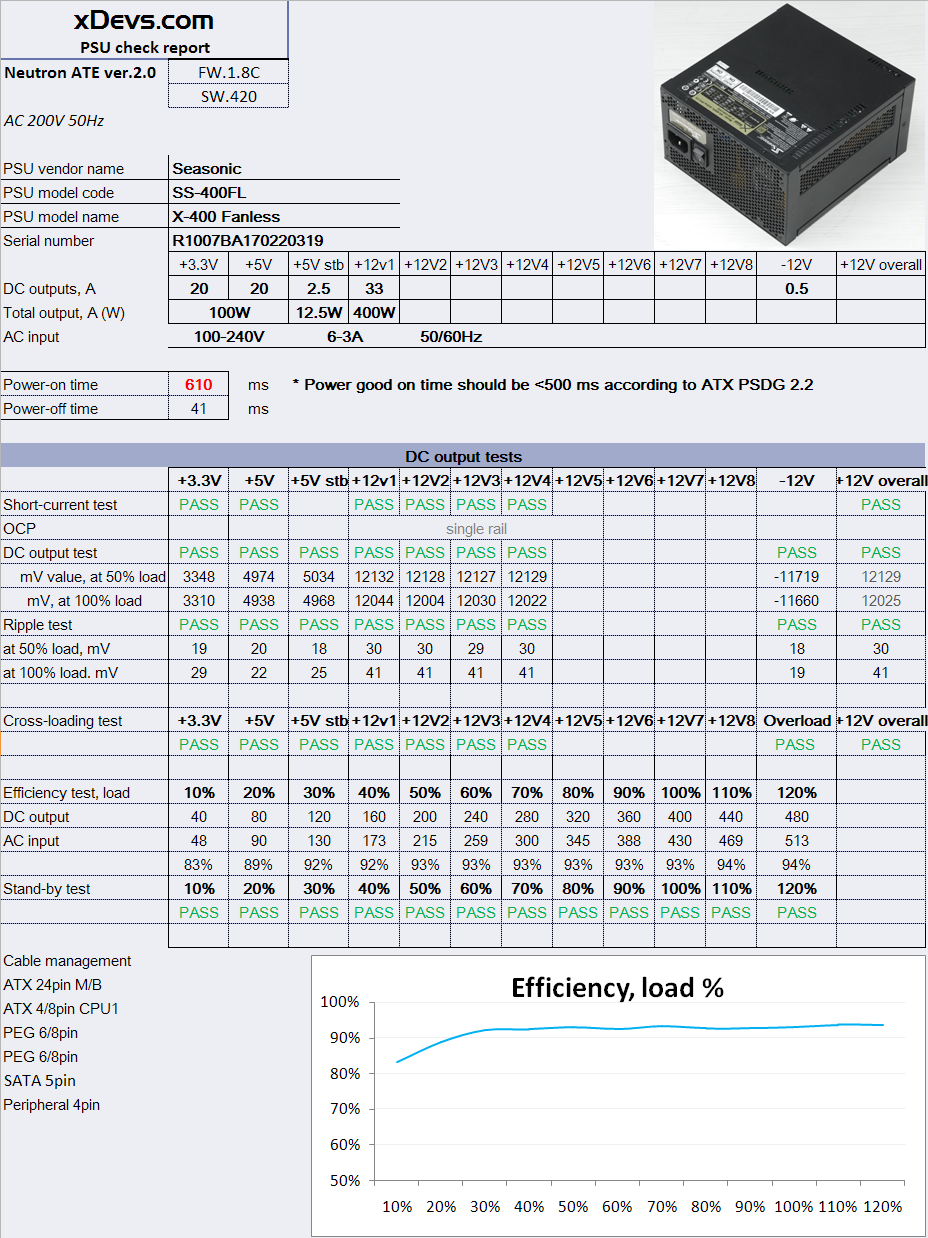
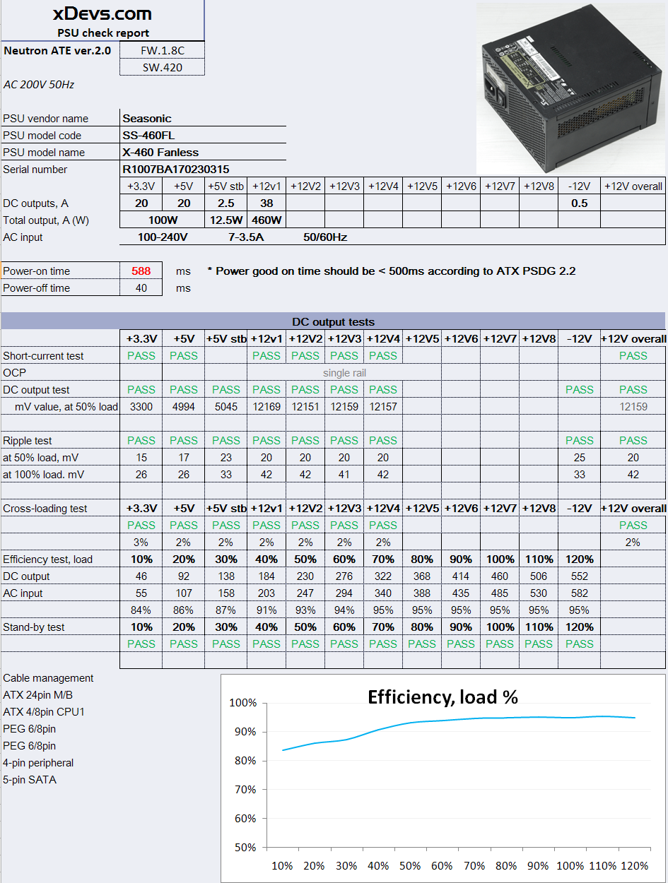
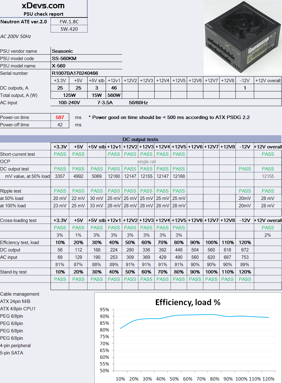
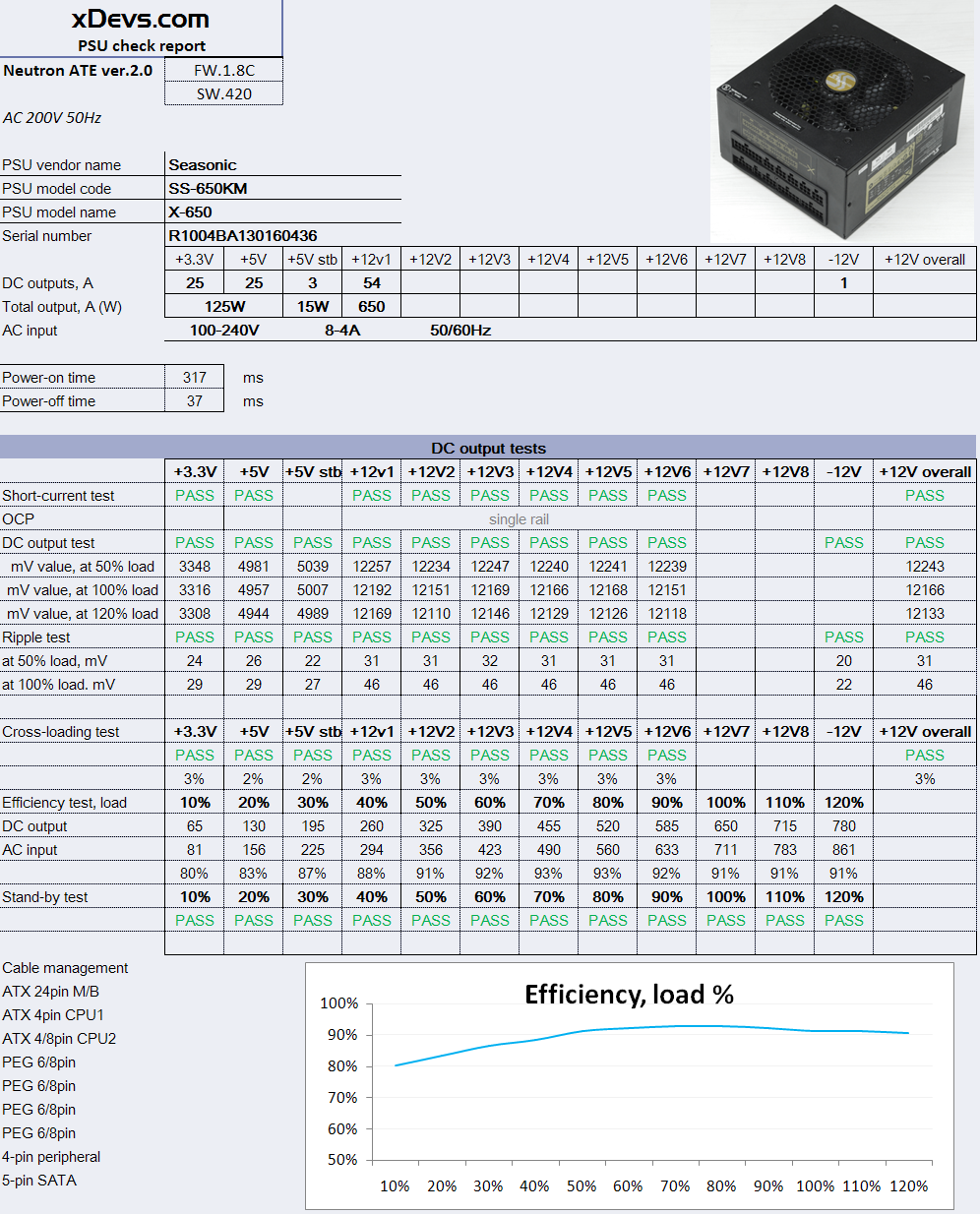
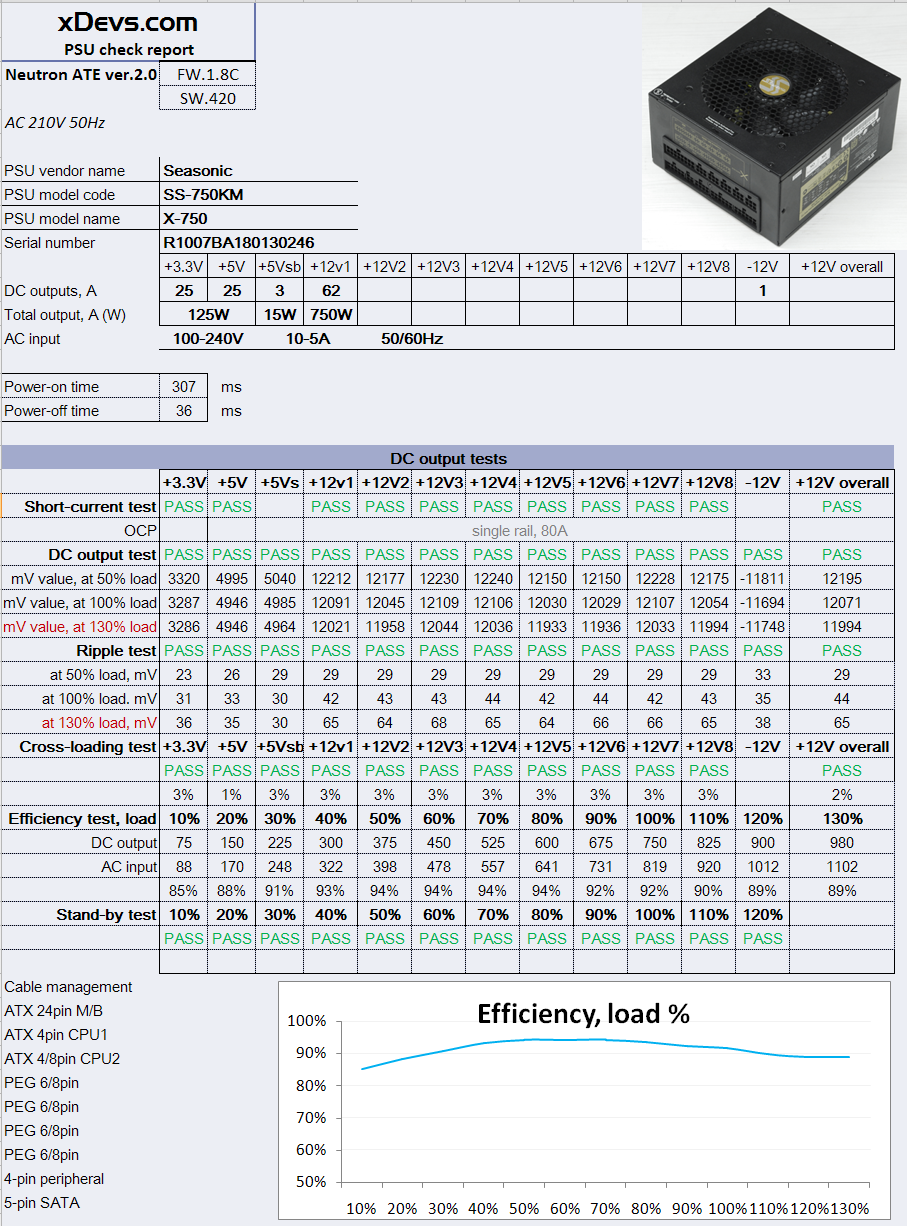
Seasonic PSUs testing example
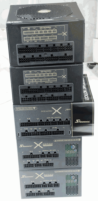
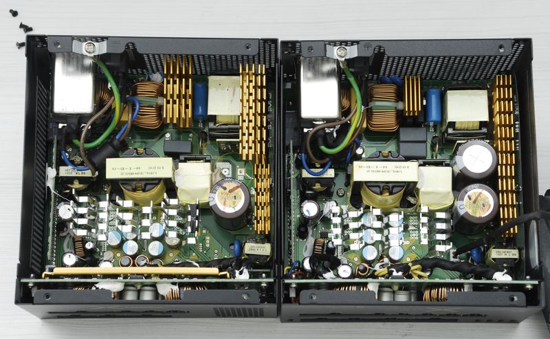
Let’s put few Seasonic X-series ATX PSUs thru testing with Neutron. Models are 400W and 460W Fanless and 560W, 650W, 750W. All 80Plus Gold, high efficiency, enthusiast targeting, high-end assembly and features. These PSUs are not cheap, so I expect great results.
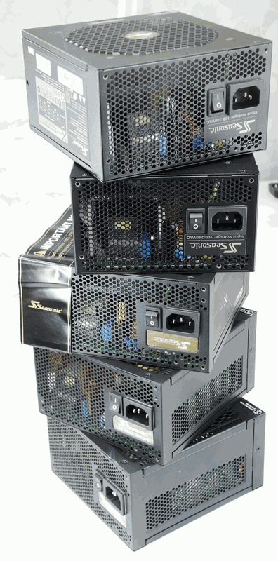
Peek inside the PSU:
And test results, on various graphs:
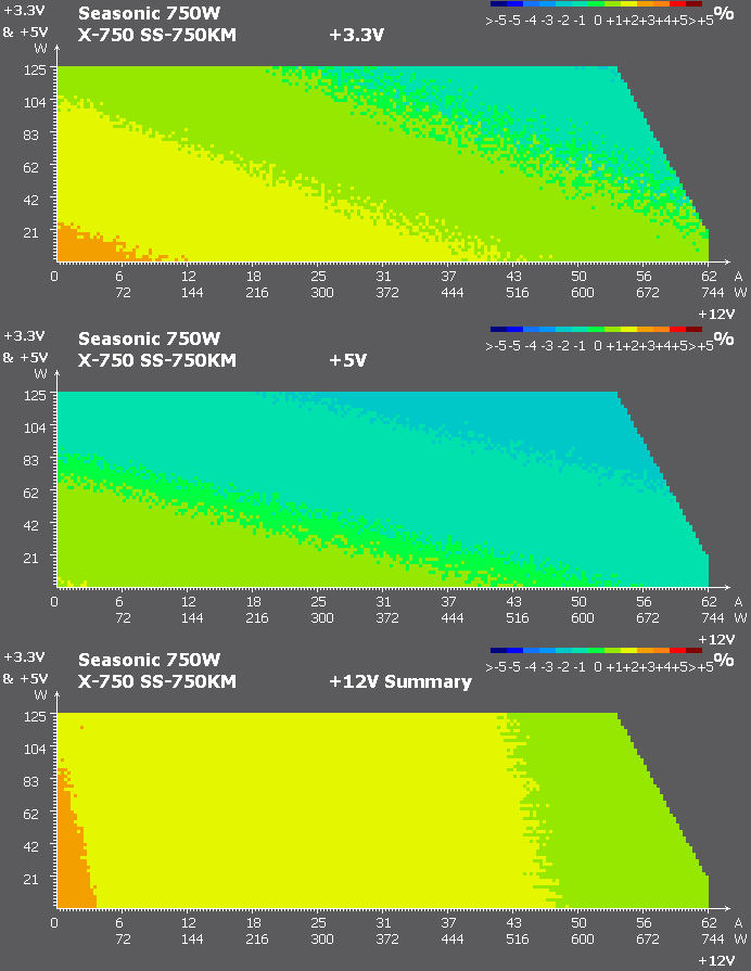
During OCP testing high limit was quickly discovered, allowing even 975W of loading at 750W-rated power supply.

You may think this is extreme case, and everything was out of spec, but that was not the case at all. Look at regulation results on 980W loading screenshots below!
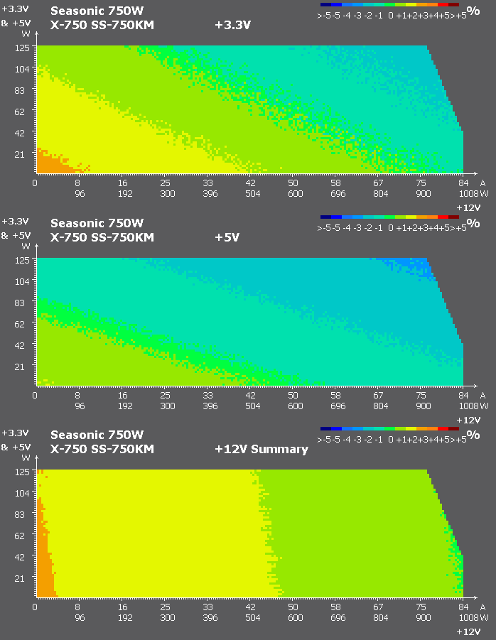
Extended cross-loading chart with up to 1000W peak.
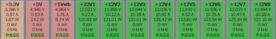
And final results for all power supplies:

Final note and summary
Time spent on this project
- Project idea and prototyping with one channel MOSFET load (1 month)
- Schematics design (1 week)
- Layout design (2 weeks)
- Assembly (1 week)
- Calibration (2 weeks)
- Testing and stress-testing (2 month)
Total BOM cost of everything, including Chieftec ATX Fulltower chassis was $800 USD, which is less than price of single channel DC load from top tier vendors, so our goal of very cost effective test setup was achieved, with account of 1% DC performance level.
Final evaluated specifications can be listed as below:
DC load channels
- Channel qty: 12 independent (1 extra, reserved)
- Max input voltage : 0-15 VDC for all, -24…0 VDC for negative -12VDC
- Peak input voltage: 30 VDC
- Max current, per channel : up to 25АDC
- Maximum infinite power, per channel : 240W
- Current setting resolution : better than 100mADC
- Current regulation accuracy : better than 1% (<1ADC load)
- DC voltage measurement accuracy : better than 0.5%
- DC current range : 0 – 30 ADC
- DC current accuracy : better than 1%
- Sampling speed : 500 kSPS
- Input voltage noise measurement bandwidth: DC-150kHz
- Noise resolution : 10 mV(RMS)
- External probe ports : Yes, per channel, SMA DC coupled
- Cooling system : 6 x high-power 120х120х38 +12VDC fans
Please also keep in mind a fact, if I would be designing such system today, many things would be done differently, and likely using more ready solutions. Good example would be standard current sensing chipsets, like Texas Instruments INA3221. Also calibration can be done automatically with addition of multiplexer and known reference +10V and 1ADC source onboard. Addition of AC mains side measurement module with energy-metering chip like Analog Devices ADE7953 (PDF) could aid automating and efficiency measurement tests and evaluation as well.
Currently there are no plans to revise and redo this project, but I will be happy to reply any questions regarding ATE systems and PSU testing.
Projects like this are born from passion and a desire to share how things work. Education is the foundation of a healthy society - especially important in today's volatile world. xDevs began as a personal project notepad in Kherson, Ukraine back in 2008 and has grown with support of passionate readers just like you. There are no (and never will be) any ads, sponsors or shareholders behind xDevs.com, just a commitment to inspire and help learning. If you are in a position to help others like us, please consider supporting xDevs.com’s home-country Ukraine in its defense of freedom to speak, freedom to live in peace and freedom to choose their way. You can use official site to support Ukraine – United24 or Help99. Every cent counts.
Modified: Feb. 25, 2016, 6 a.m.