This is work in progress project, updates will be posted frequently.
Motivation for this work
Over the last few years xDevs collective accumulated rather nice set of electronics and meteology equipment that can rival some commercial calibration labs. But given limited resources and research only approach most of such equipment is idling at best, waiting for occasional use. This is not very efficient nor environmentally friendly. In this article goal to repurpose such idling equipment is set.
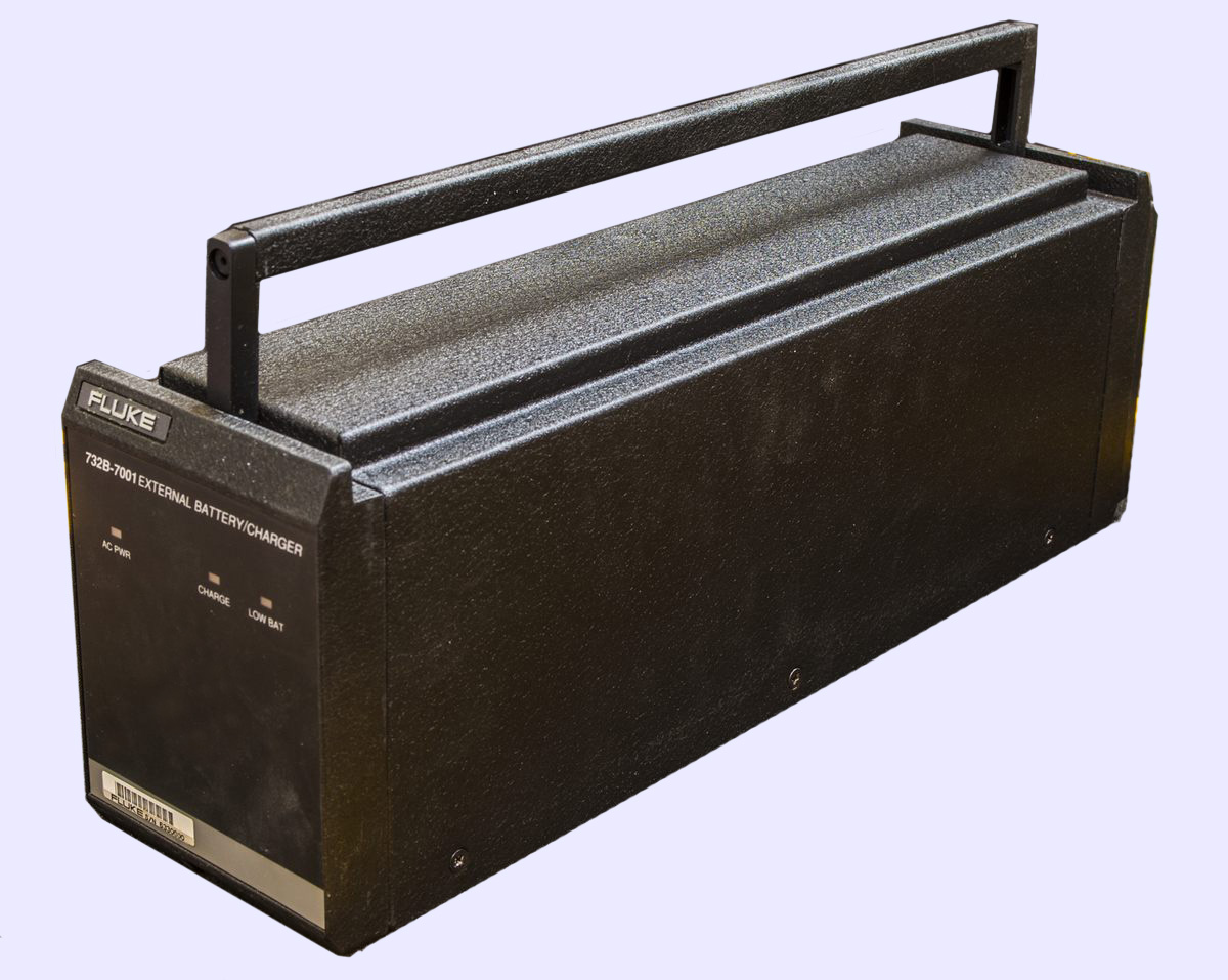
In more specific words, we have number of Fluke 732B-7001 battery chargers, which are companions for famous Fluke 732B zener 10V reference DC voltage standards. But because such standards are 99.9% of time just sitting in a crate slowly drifting over time these backup chargers are just doing nothing. Idea here is to turn them into something useful and practical for metrology lab.
First, lets get familiar with these 732B-7001 chargers. They reuse exactly same chassis as actual 732B reference but have missing the magical DC reference assembly and it’s oven. Because of this there are also no output binding posts or any terminals on front panel.
!
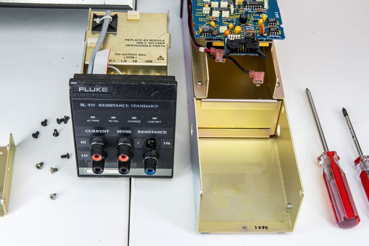
Below is photo of gutted charger and Fluke SL935 prototype ovenized module
Now what can be more useful for ppm volt-nut then yet another DC voltage reference out of it? We already have nice enclosure, battery and Fluke original battery charger/power supply inside. Just need add a little reference inside and output binding posts and job well done. Sounds easy for a quick weekend project?!
Project LX design targets and goals:
Key goals for this project were established as following:
- Single 10 VDC output
- Long-term stability better than 0.5 ppm/year
- Power supply rejection ratio better than 0.01 ppm (AC or battery)
- 4-wire capability with true remote sense
- Ability to source and sink current with 25mA compliance, less than 0.001 &Omega output resistance.
- Recovery time after power up under 2 hours
- Electrical isolation better than 100 GΩ between output and other terminals.
- No adjust elements in critical feedback path
- Less than 10kg weight with battery
- Provision for external DC IN power to extend battery life
- Easy interface with 5-way binding posts
- Ability to monitor internal temperature and reverse polarity of the output.
- Output noise better then 0.08 ppm ptp 0.1-10 Hz
- Temperature coefficient better than 0.02 ppm/°C
- Battery operation for at least 80 hours
- Total project cost $1000 USD (732B charger cost excluded)
- 100 human-hours to first working prototype, 500 human-hours for project total
Disclaimer
Redistribution and use of this article, parts of it or any images or files referenced in it, in source and/or binary forms, with or without modification, are permitted provided that the following conditions are met:
- Redistributions of article must retain the above copyright notice, this list of conditions, link to this page (/article/lxref/) and the following disclaimer.
- Redistributions of files in binary form must reproduce the above copyright notice, this list of conditions, link to this page (/article/lxref/), and the following disclaimer in the documentation and/or other materials provided with the distribution, for example Readme file.
All information posted here is hosted just for education purposes and provided AS IS. In no event shall the author, xDevs.com site, or Fluke or any other 3rd party be liable for any special, direct, indirect, or consequential damages or any damages whatsoever resulting from loss of use, data or profits, whether in an action of contract, negligence or other tortuous action, arising out of or in connection with the use or performance of information published here.
If you willing to contribute or have interesting documentation to share regarding pressure measurements or metrology and electronics in general, you can do so by following these simple instructions.
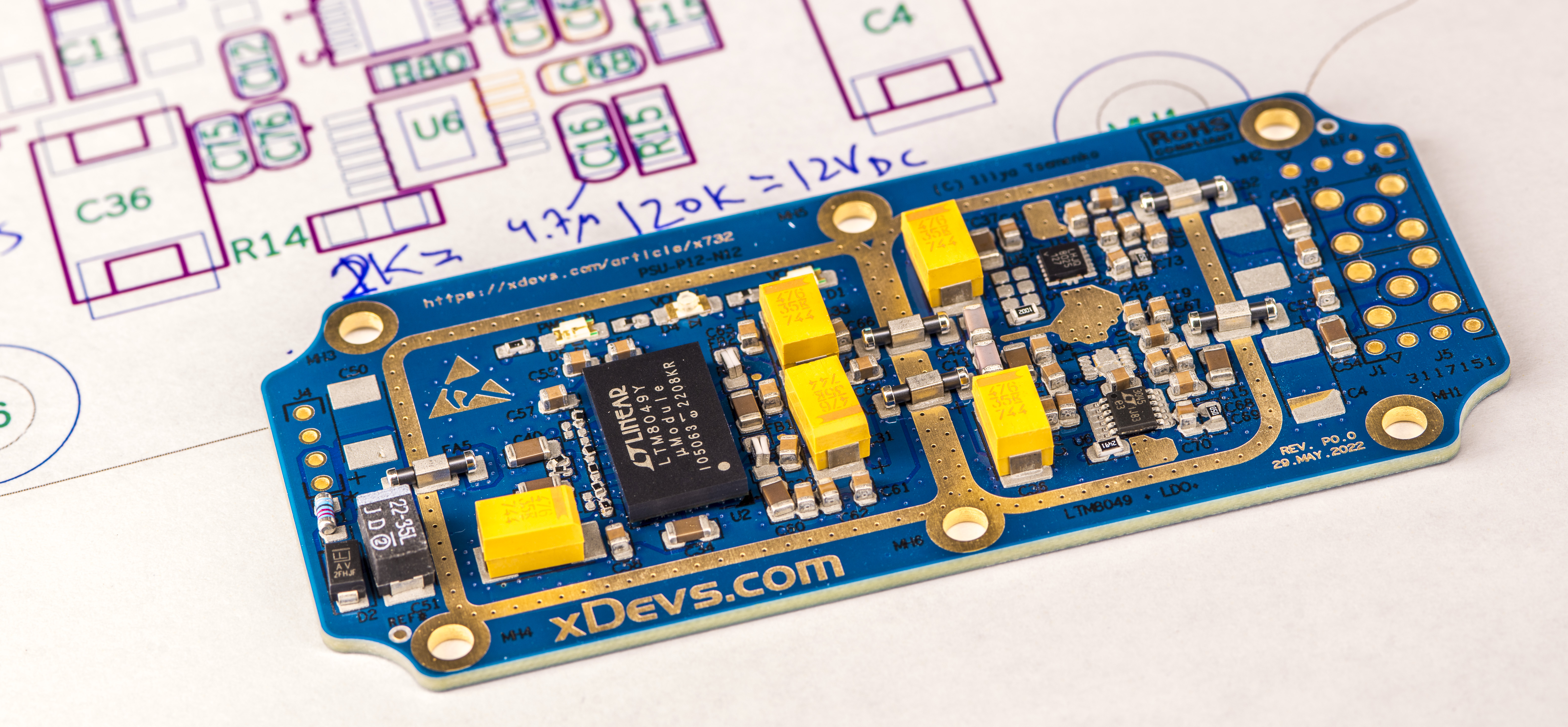
LX Project design
This project progress is also tracked internally here.
Overall idea can be presented in following block diagram
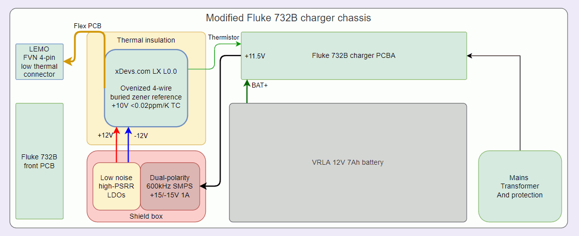
Switch mode bipolar power supply
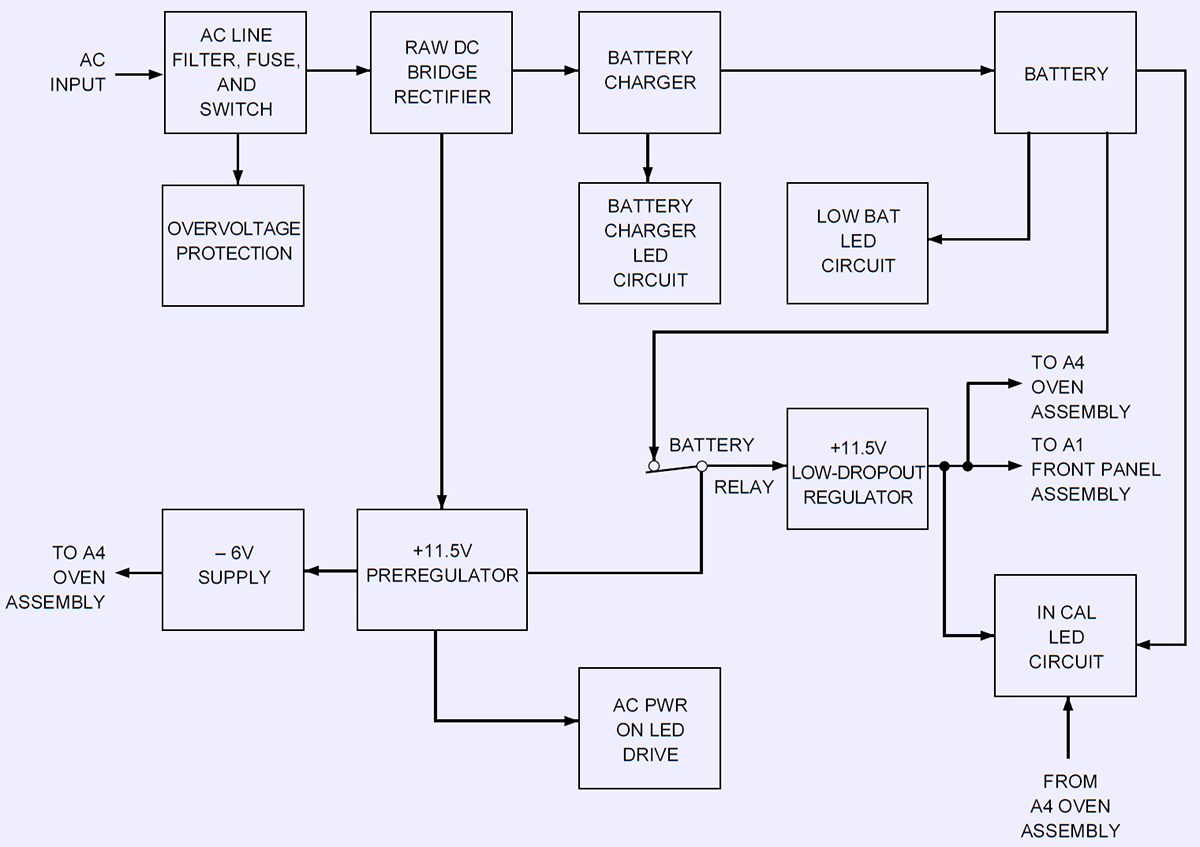
Since design target require reference to have both sourcing and sinking current capability this renders need in bipolar power for output driver. But there is a problem – 732B charger PCBA provides main positive +11.5 VDC rail and rather weak -6 VDC from Linear LT1043 switching capacitor invertor. This shortcoming did not affect earlier project with FX reference build because Fluke 792A power pack equipped with two separate 12V VRLA batteries to provide bipolar power. Fluke 732B unit enclosure is much smaller and has only single 12V lead-acid battery as result.
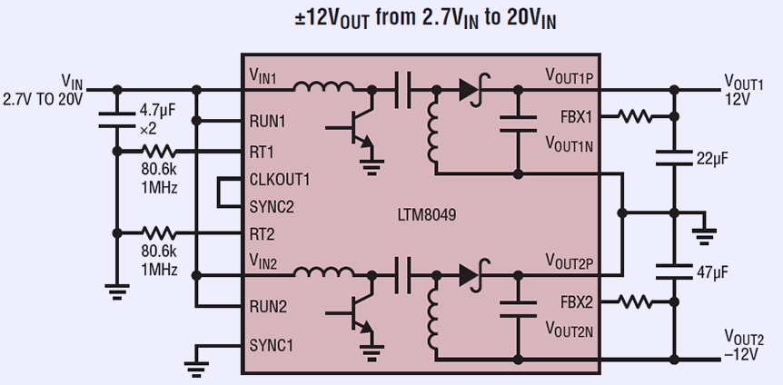
One of possible workaround to get higher current capability bipolar supply is to build our own DC-DC module to provide higher bipolar power capability. Given small available room and limited battery capacity such design have to be rather efficient and also not cause lot of issues such as EMI radiation, noise and ripple. Also I did not want to try many different solutions with discrete circuits, transformers and bread-boards but rather fit limited man-hours into this build. As result heavily integrated solution around Linear LTM8049 SEPIC\inverter was chosen.
The Linear (now Analog Devices) LTM8049 package include active power devices, inductors, all needed control circuitry and auxilary passive components. This fully integrated design allows quick and easy implementation of efficient power supply solution just with single BGA package and small set of input and output capacitors and few configuration resistors.
Many beginner engineers weary of using BGA because of additional design aspects and assembly equipment requirements. Component packaging technology is constantly evolving. We had large thru-hole discrete parts in initial years of semiconductor advancement. Then integrated circuits into small scale dies and wide scale of DIP/hybrid packages emerged. Drive to bring packaging cost lower and obtain higher integration density gave life to SOIC, QFN and DFN. Today’s higher and higher speeds require packages with less parasitics, lower power with denser interconnect, together with easier production PCBA manufacturing. BGA and its variants such as LGA, WLCSP are such advanced packages.
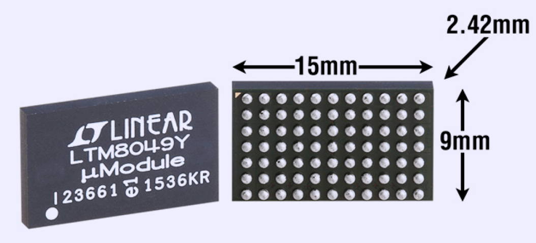
And with careful design BGA type assembly is doable even without access to some fancy expensive equipment. It is actually easier to build and assemble brand new PCBA from scratch with BGA package then repairing already assembled board. This switch-mode power supply with BGA-type LTM8049 package can be used as excellent example of assembly process with limited tools available. Large 1.27 mm pitch is rather forgiving for beginners as well, which is helpful here. And cost of $30 USD/part is also very motivational for doing good design and double-checking everything :) .
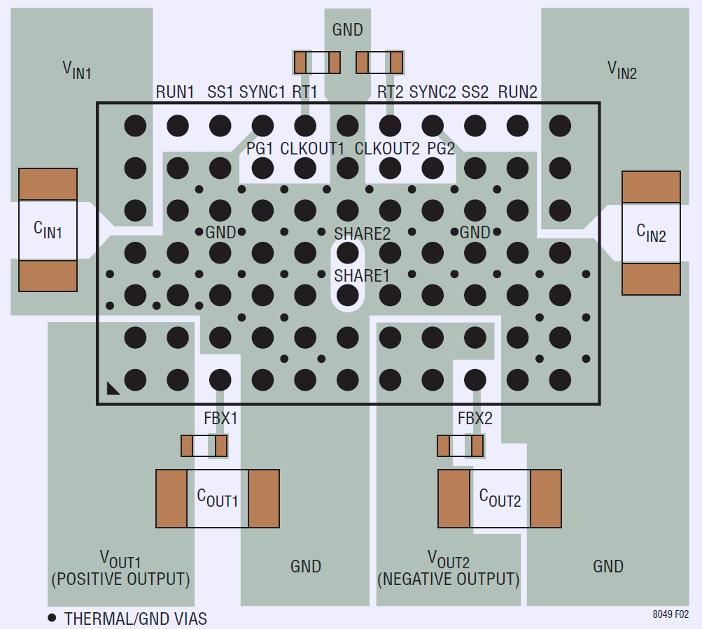
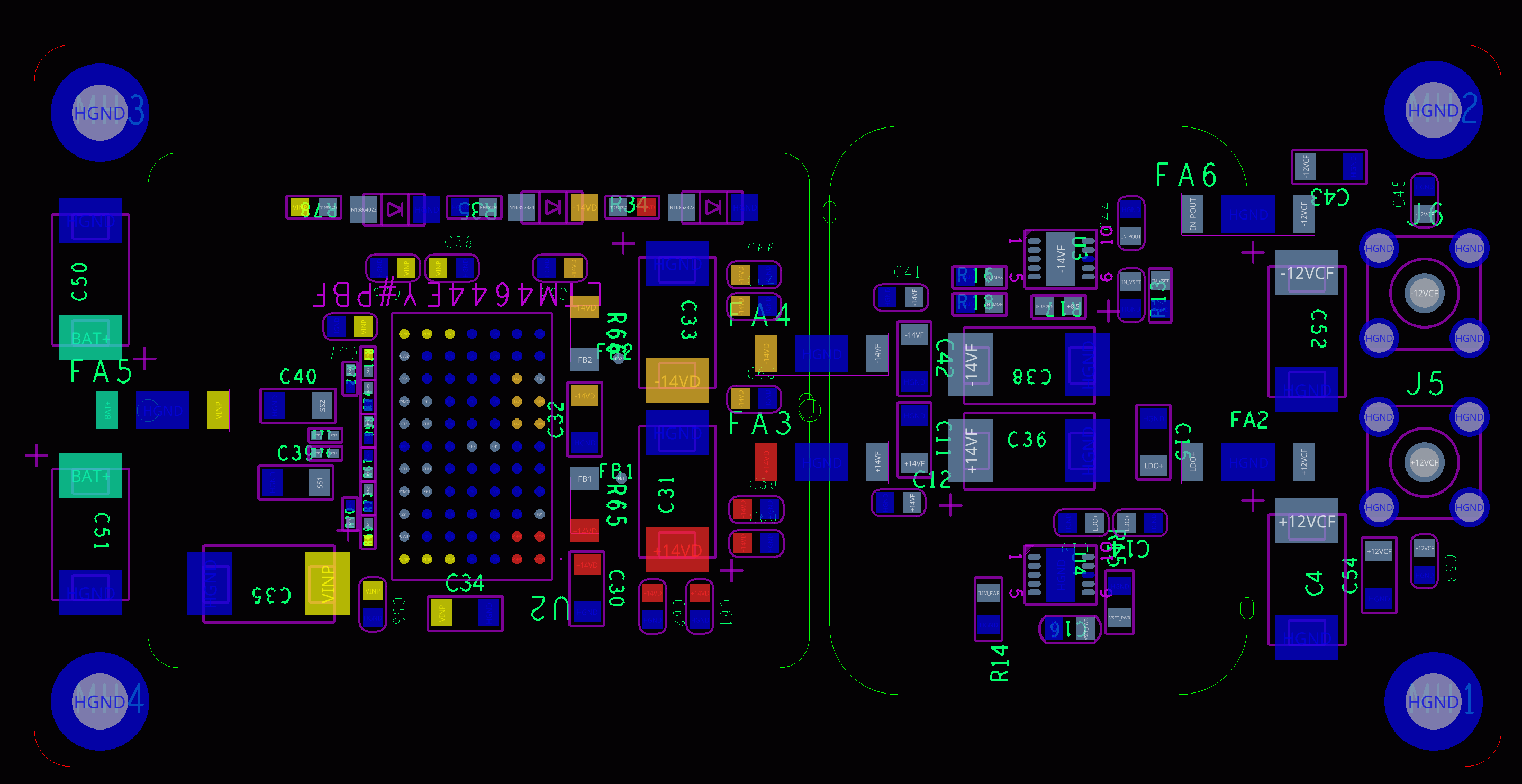
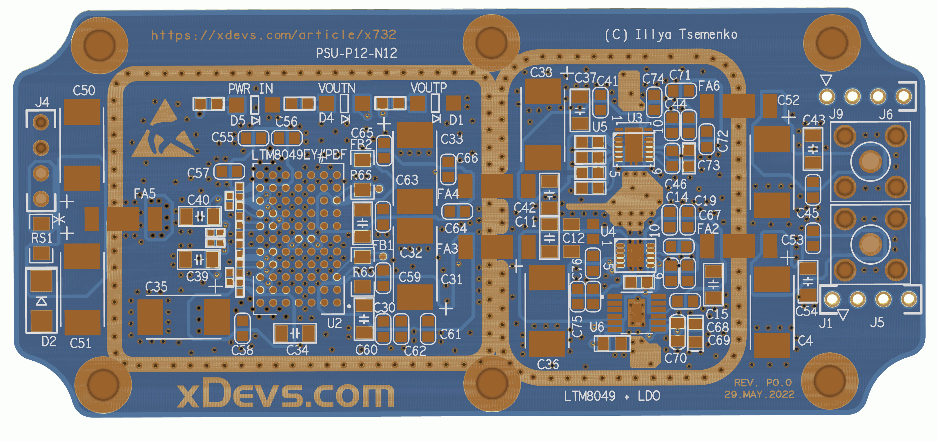
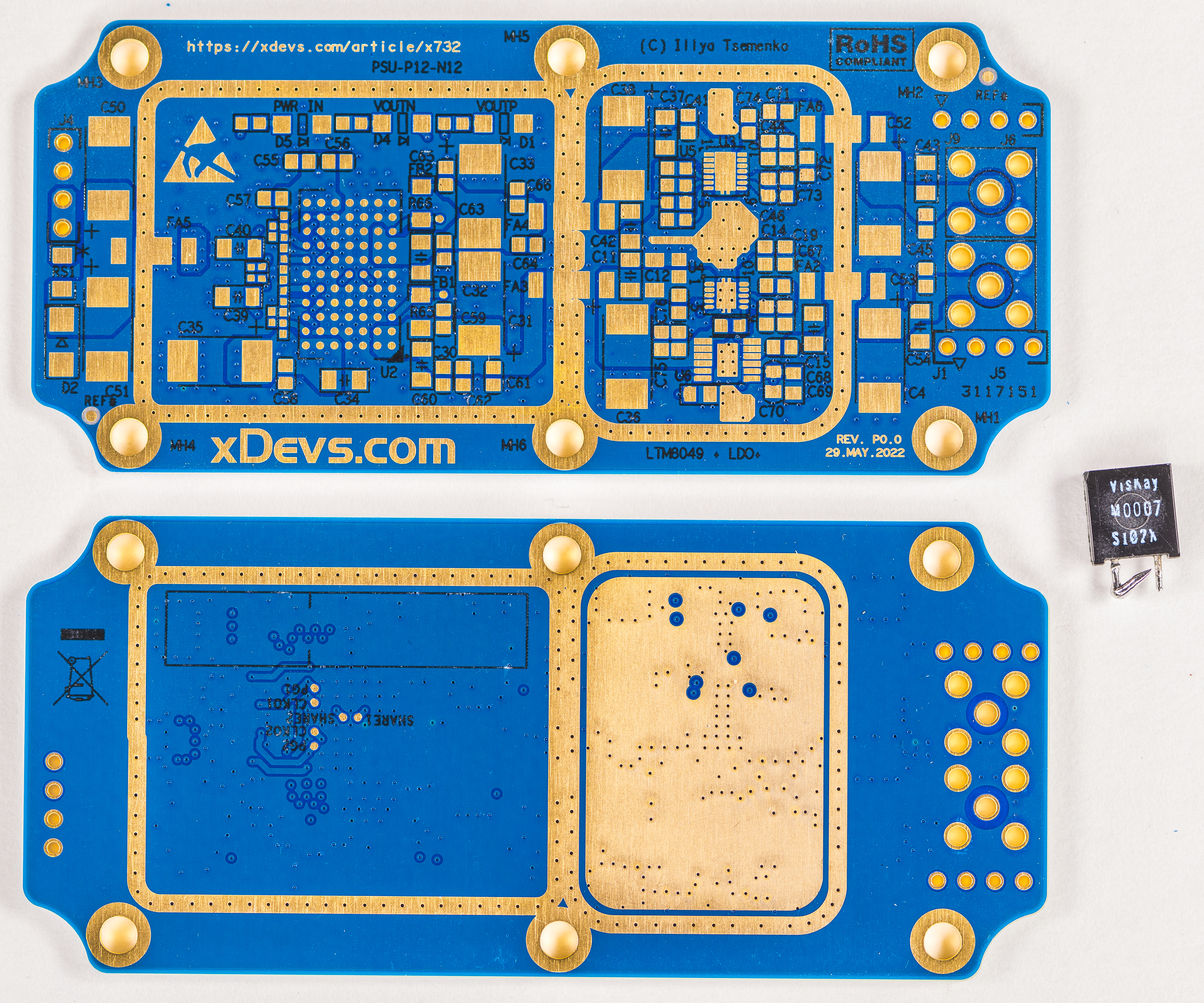
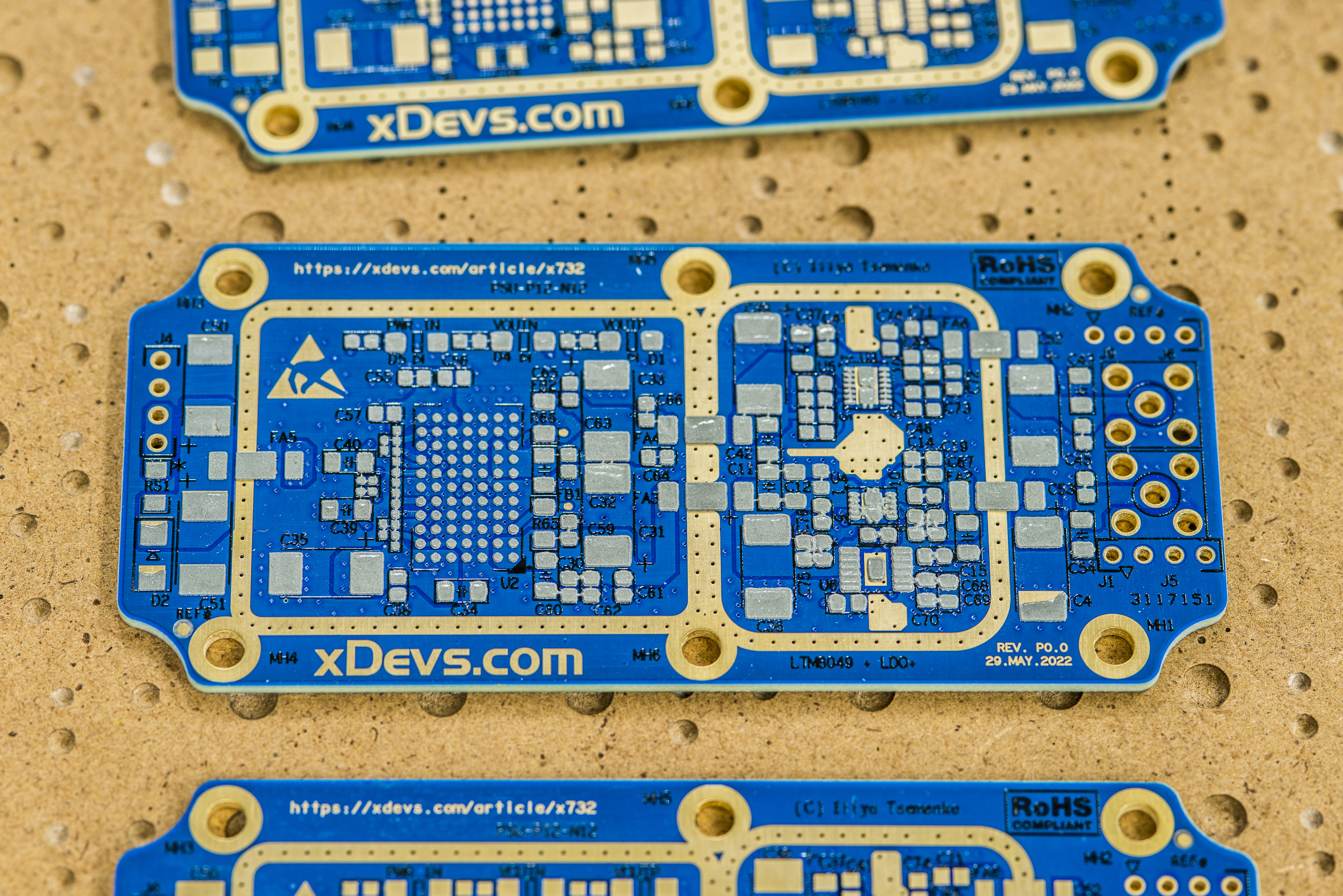
Highly optimized ballmap layout of LTM8049 allow easy routing, possible even with sub-optimal two layer PCBs. In this design we’ll use better four layer design to help with thermal transfer and power delivery. Integration of inductors and all power switching components inside BGA module limits noisy “hot” switching loops small and confined around LTM module itself. Optimal layout is also provided in datasheet, so it’s a good starting point for design.
Few design choices are selected to implement the supply. Given the LX design goals switching frequency of 600 kHz selected as a middle ground between efficiency and harmonic content. Soft-start is implemented to allow gradual power supply start upon power on. PCB design flexible configuration for input and output capacitors so we can fine-tune the actual BOM and used capacitor layout based on performance tests.
Typical output ripple with LTM8049 alone expected to be around 50mV peak to peak. To reduce that noise further post-regulator with linear regulators LT3045 and LT3094 will be used. These regulators have excellent PSRR over 60dB up to 3 MHz and able to support loads up to 500mA and ultralow RMS output noise.
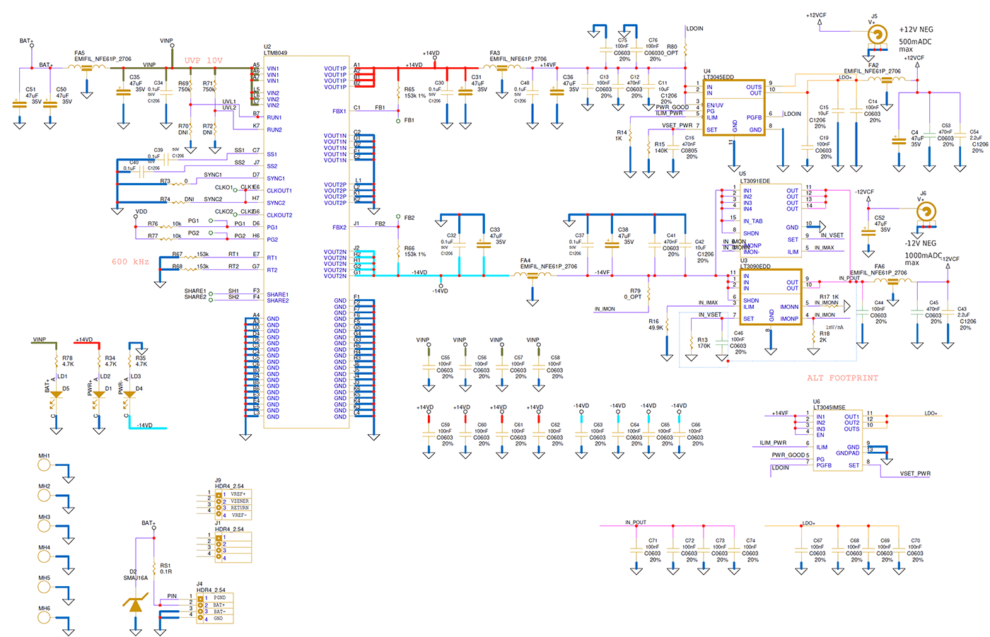
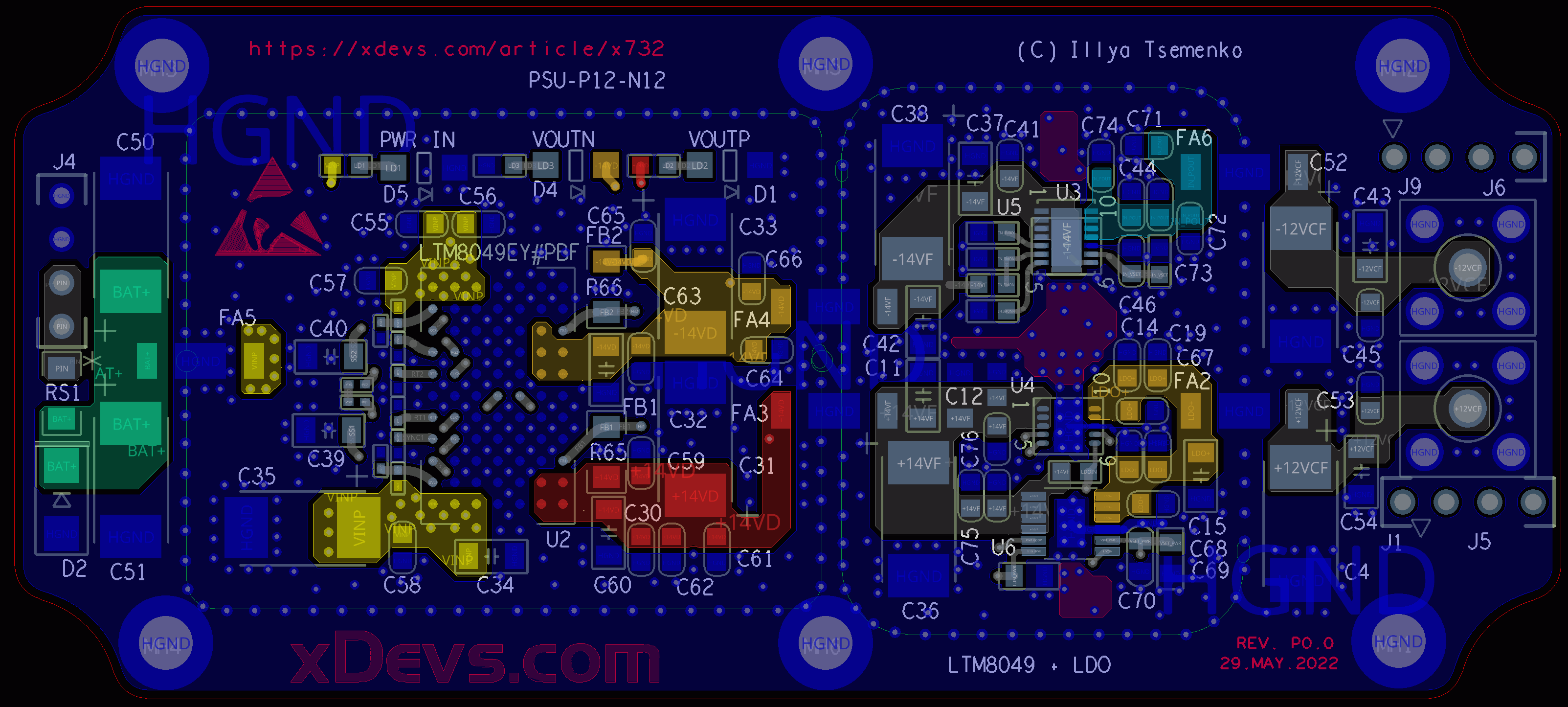
PDF Schematics for the LX switch-mode supply
PDF PCB layers for the LX switch-mode supply
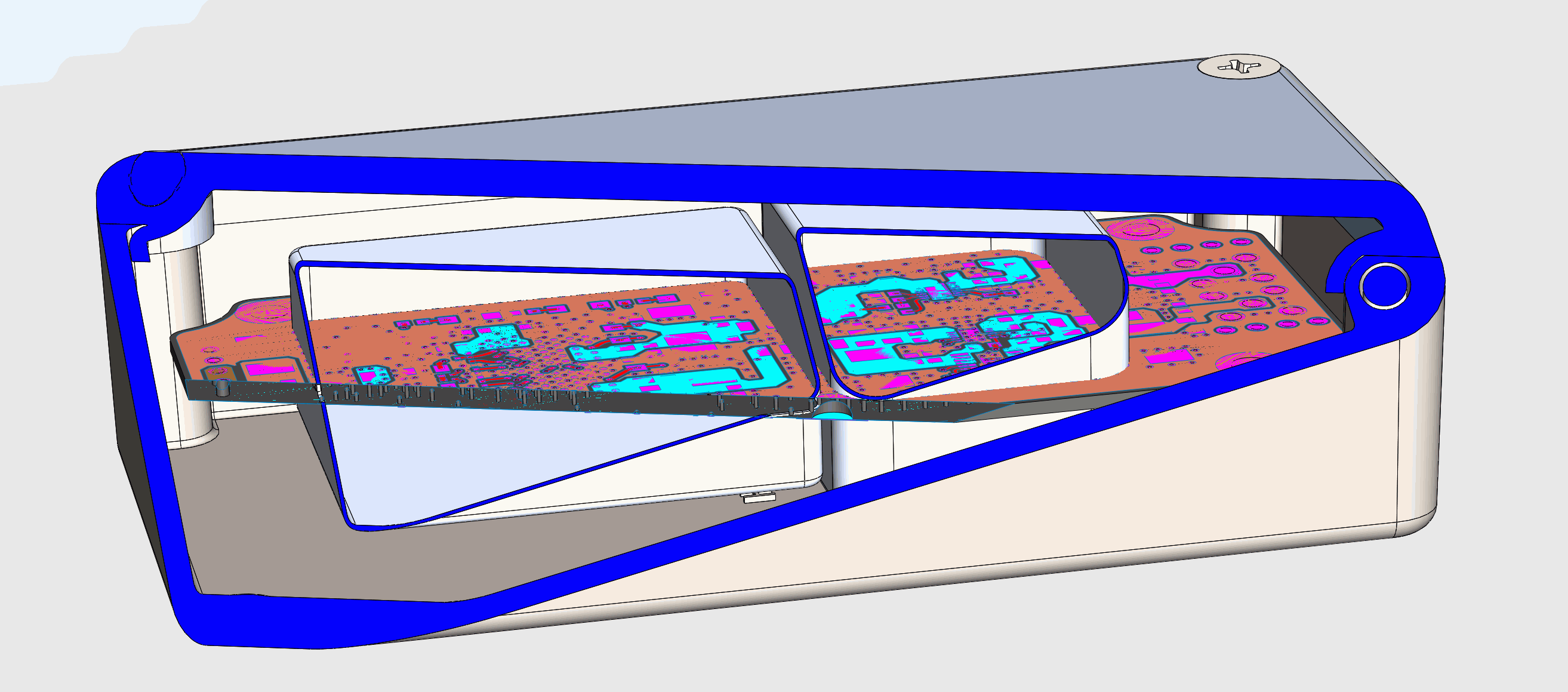
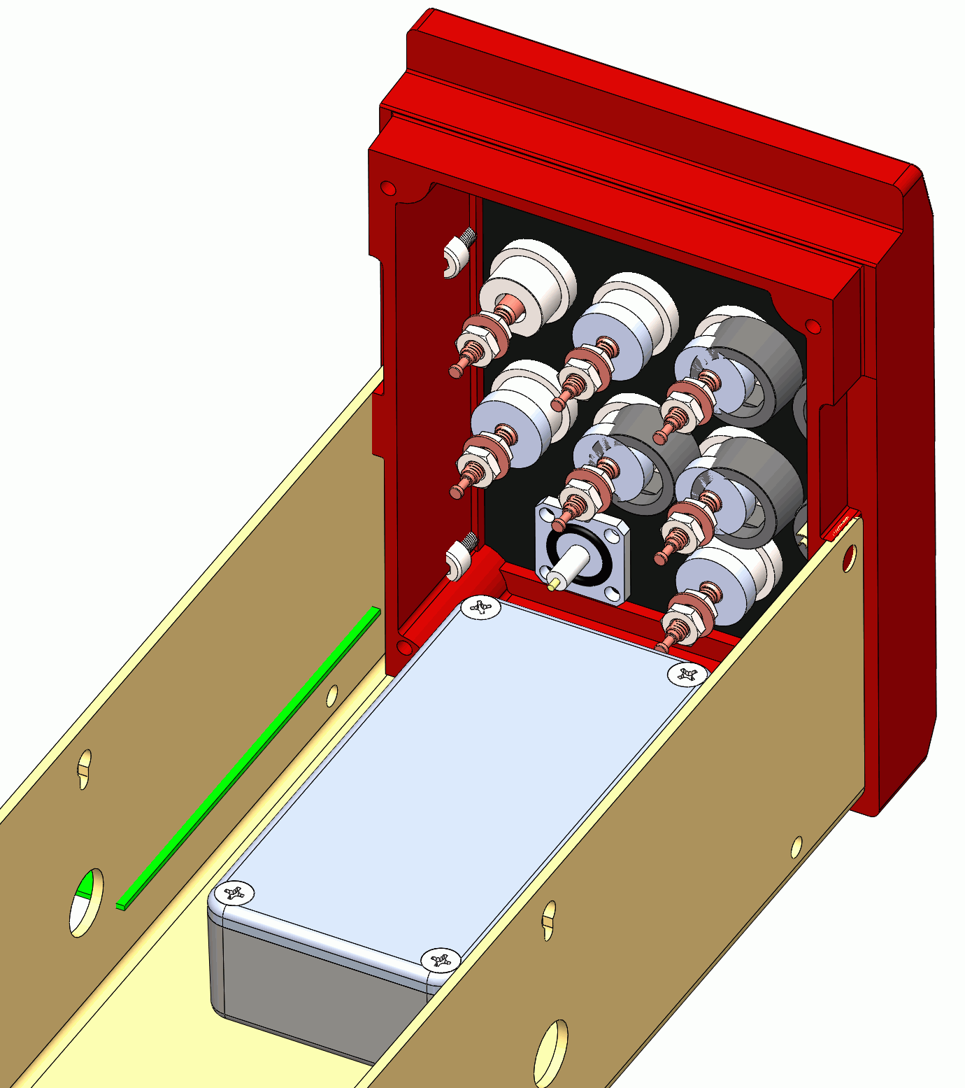
Mechanical design would incorporate double shielded construction. PCB components and separation between switch-mode supply and linear regulators done with steel cans at both sides of the board. Power rails connect via ferrite bead SMT filters.
Initial concept:
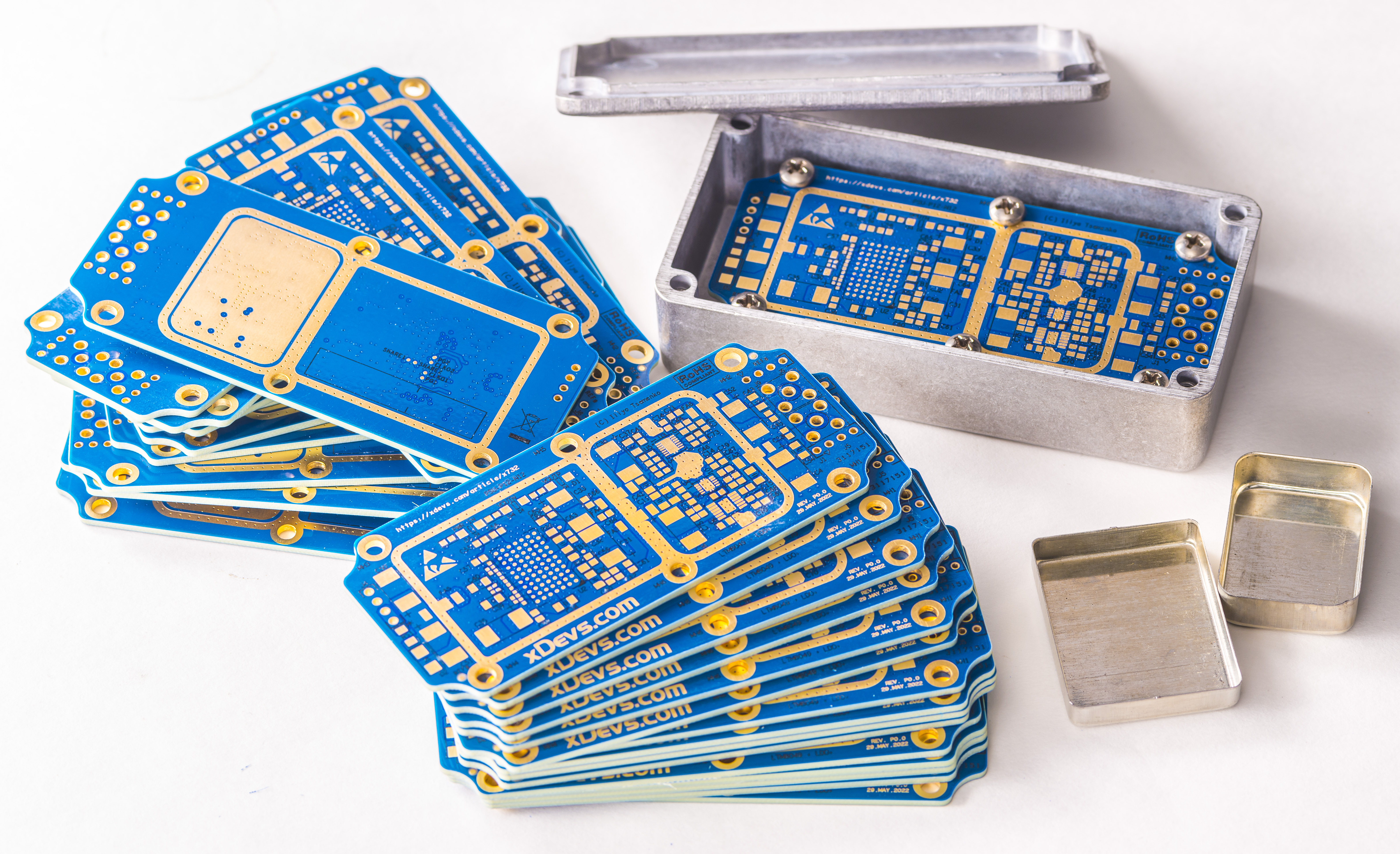
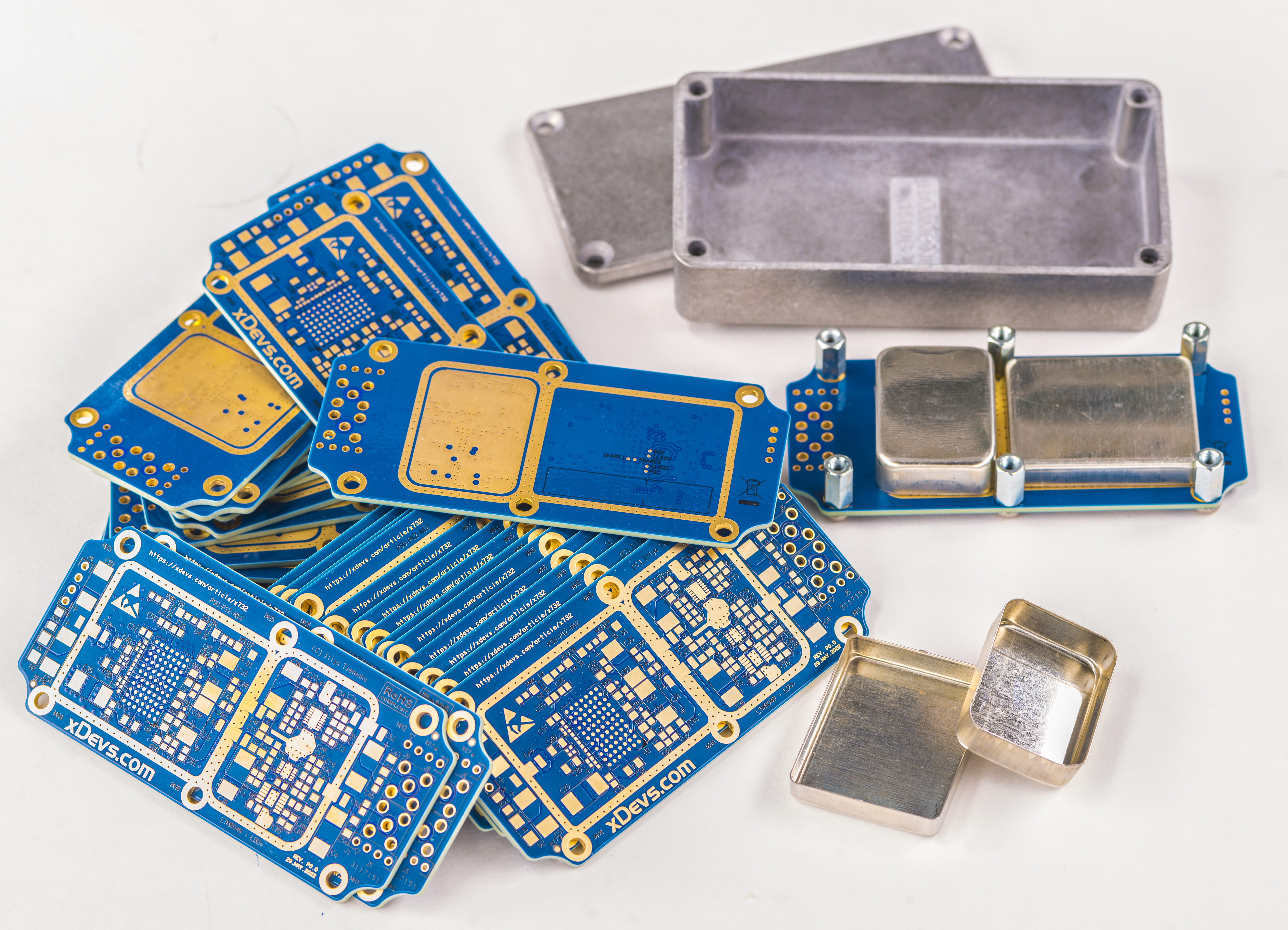
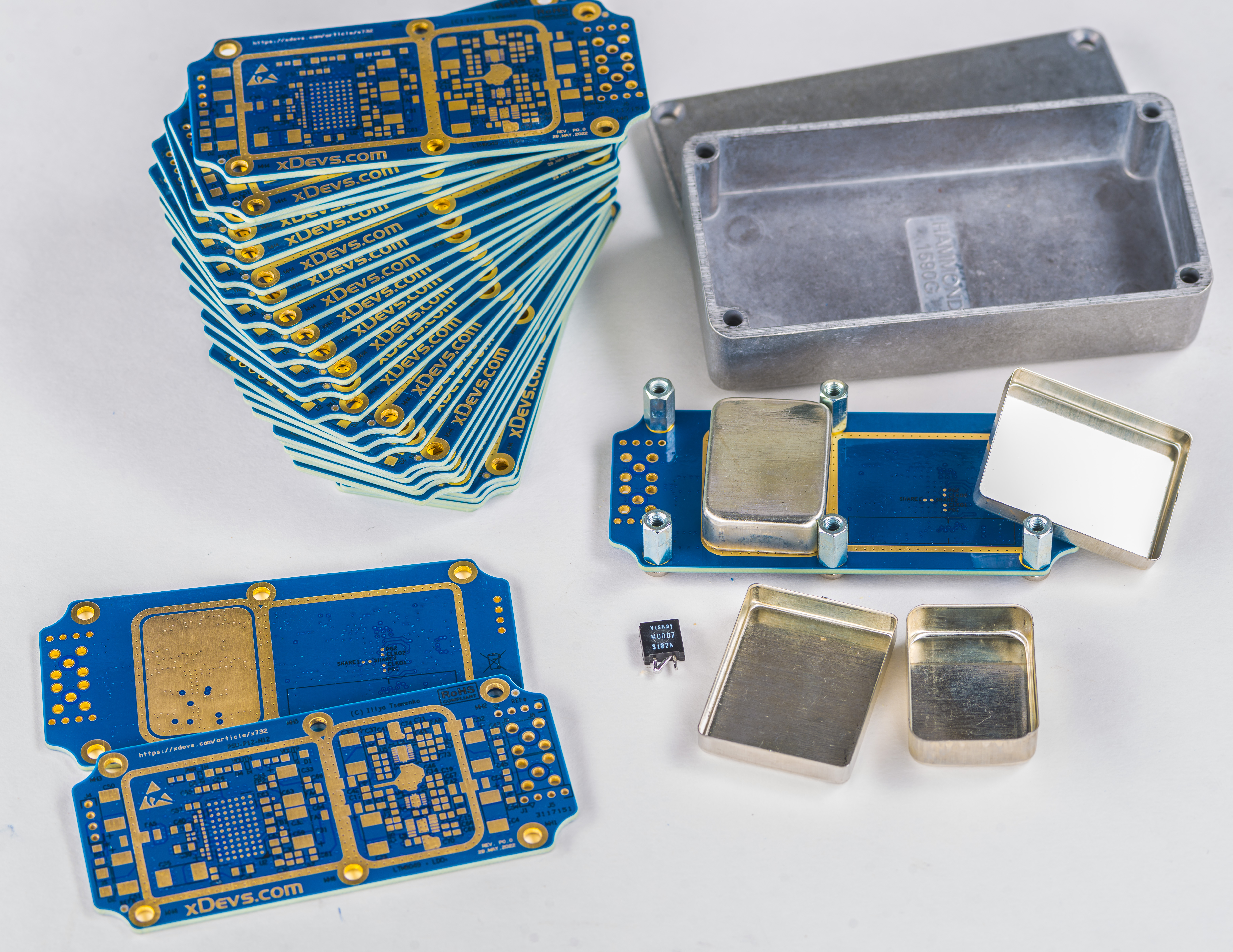
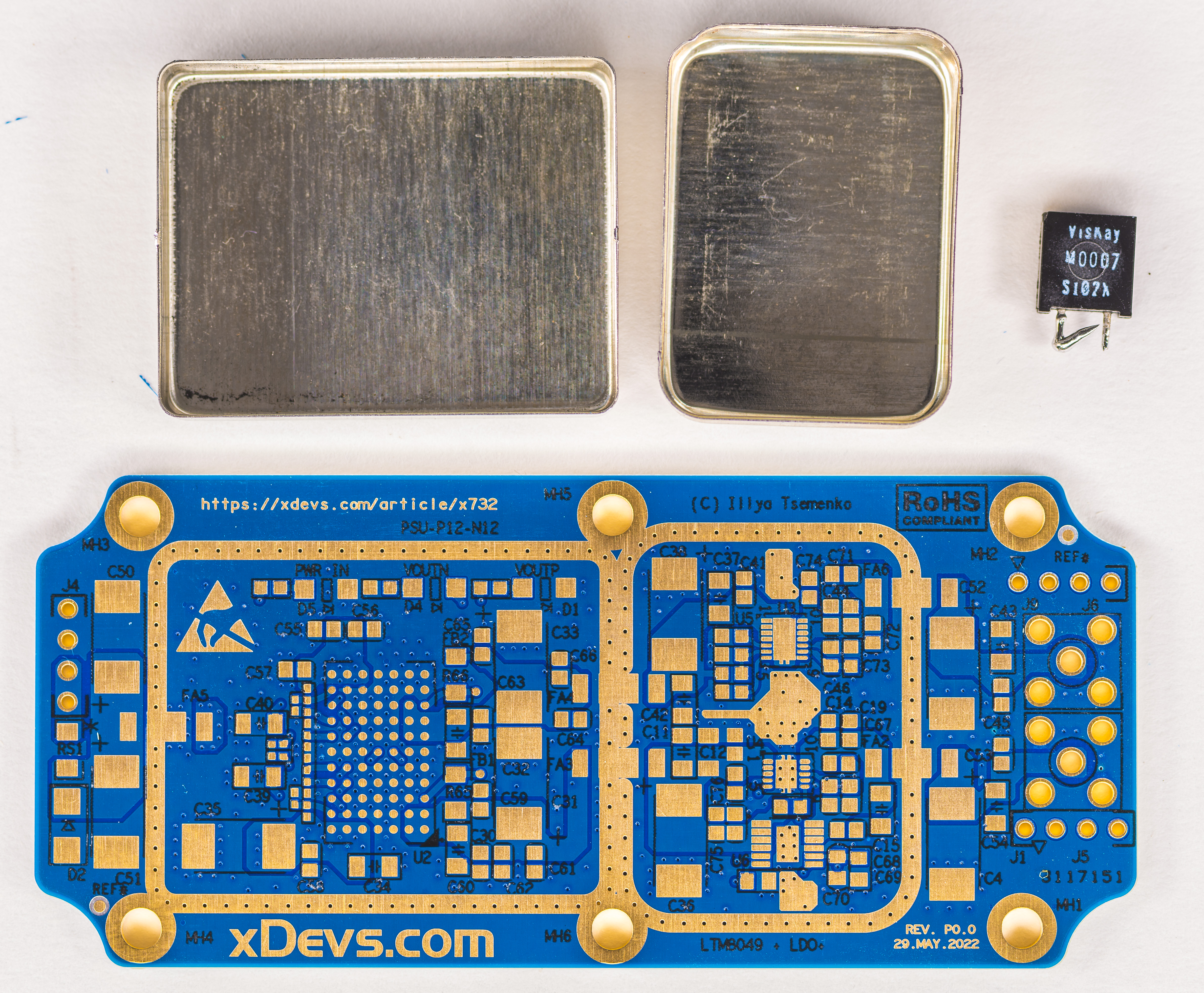
PSU PCB will have tinned steel shields soldered and sealed in the Hammond die cast enclosure.
Layout design, top layer art-work:
3D rendering of top surfaces with proposed PCB design:
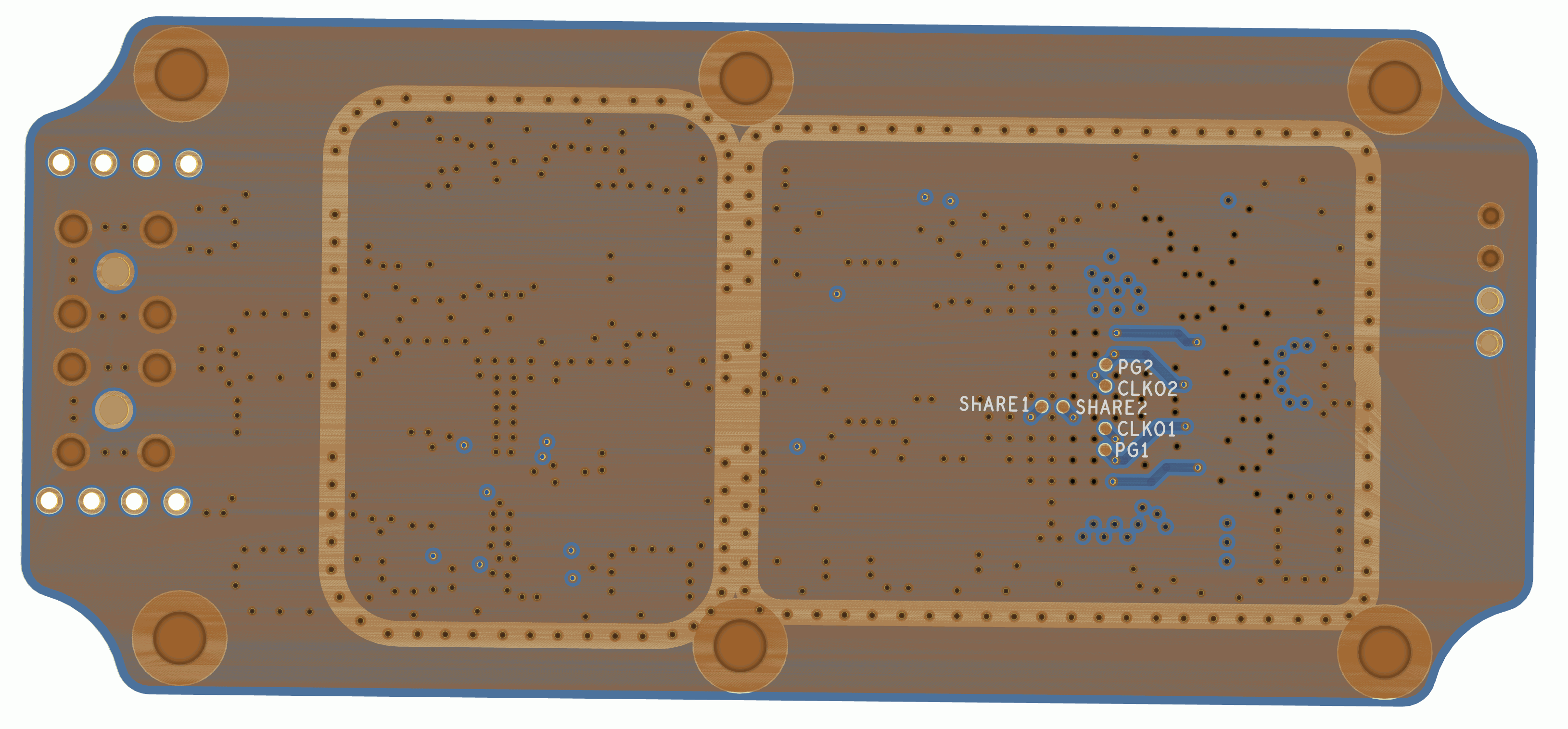
3D rendering of bottom surfaces:
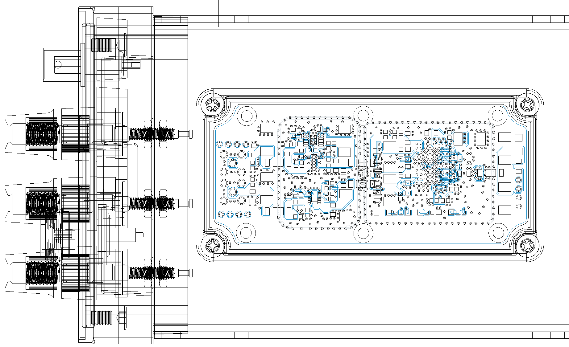
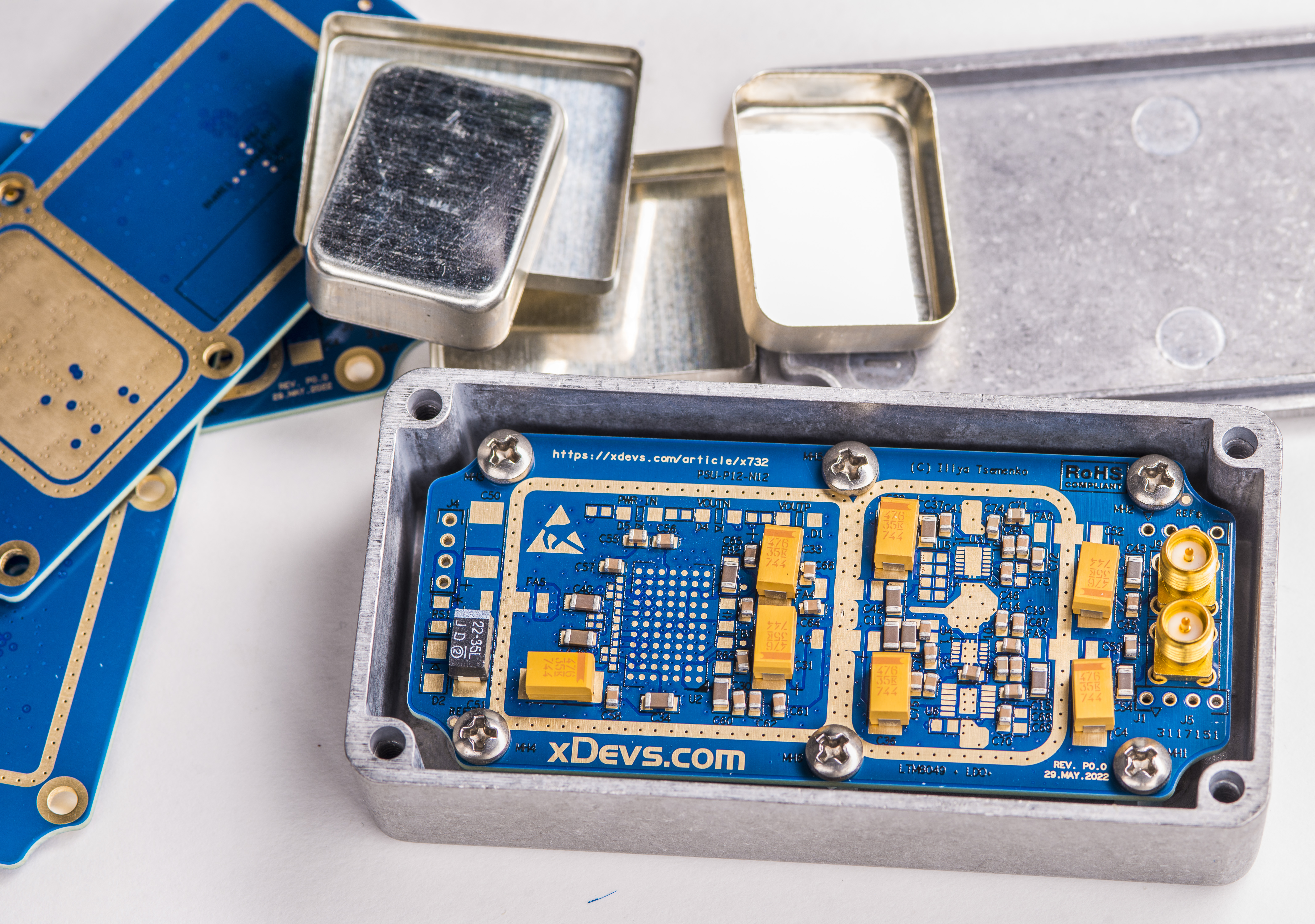
Placement concept inside Fluke 732B module.
Power converter PCB Assembly
After few weeks of waiting PCBs and parts were delivered. For this experimental prototype we may not have the best performance from first try but sure enough we can make best effort with build and assembly.

Assembly steps in details
Now we got all components and PCBs delivered, it is time to assemble the first prototype. I will show whole process start to finish both in photographs here and in video clip.

Make sure you get all components ready and have enough bench room around boards to work with parts, tools and packages. It is great to have binocular optical microscope for better placement quality, especially with today’s modern 0402, QFN and micro-BGA and similar fine-pitch parts. Here circuit board has variety of components sizes, from large D package (7343) tantalum capacitors to 0603 and 0402 passives, as well as 1.27mm pitch BGA module and 0.5mm pitch DFN. SMA Connectors will not be soldered during SMT parts assembly, we’ll solder them manually with soldering iron after everything else is assembled.
First step – application of solder paste to pads on PCB surface.
This process is similar to silk-screening, where you have thin stainless steel sheet with precisely cut slots and holes that match component pads on PCB surface. Stencils are manufactured by laser cutting thin steel sheets (usually 0.1-0.05 mm) from PCB Gerber file. If you need paste applied on both sides, you’d need separate artwork per side on the stencil.
Here with LX reference power supply I have all components only on top surface, so it is simpler to assemble. Almost all PCB houses can also manufacture and bundle steel stencils for your design, but it’s also possible to order stencil separately, for example from OSH Stencils. Prices for stencils are usually vary from $15 USD to few $100’s USD, depending on complexity, board size and additional polishing/framing requirements.
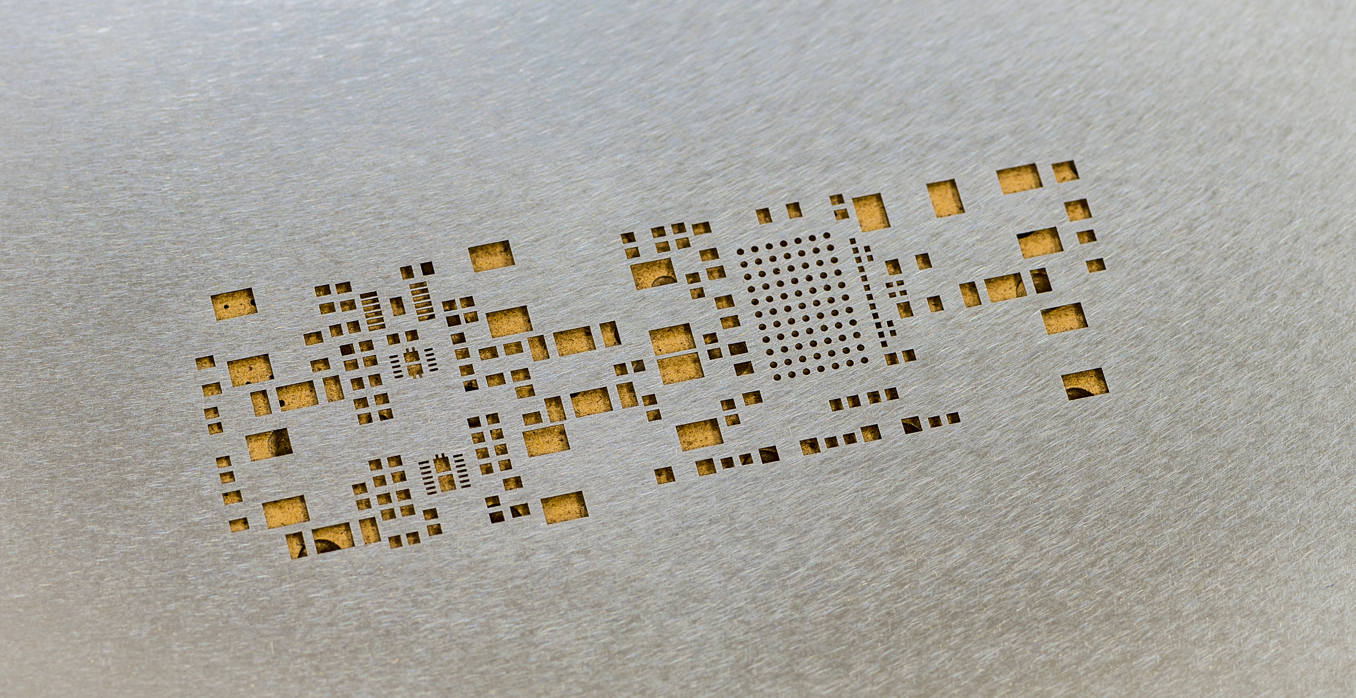
Alignment for paste printing
Next step is to put a PCB under stencil on flat steady bench and align all pads and openings of the stencil perfectly in spot to exposed pads on PCB. For production purposes stencils and PCB holder fixtures often have alignment pins to simplify and ease the process, but here it’s just alignment by hand and eyeball. We don’t have any superfine components like 0.5mm pitch BGAs or 0.4mm WLCSP, so even if stencil get misaligned for fraction of millimeter, it’s no big deal.

Applying solder paste.
Solder paste is a grey-looking goo which actually consists of super-tiny solder balls mixed with activation flux. It is conductive and quite messy. Make sure you have paper napkins, some cleaning alcohol and enough room around stencil and PCB to work with this. Best idea to handle paste with gloves, as it is not very healthy and quite hard to clean off.
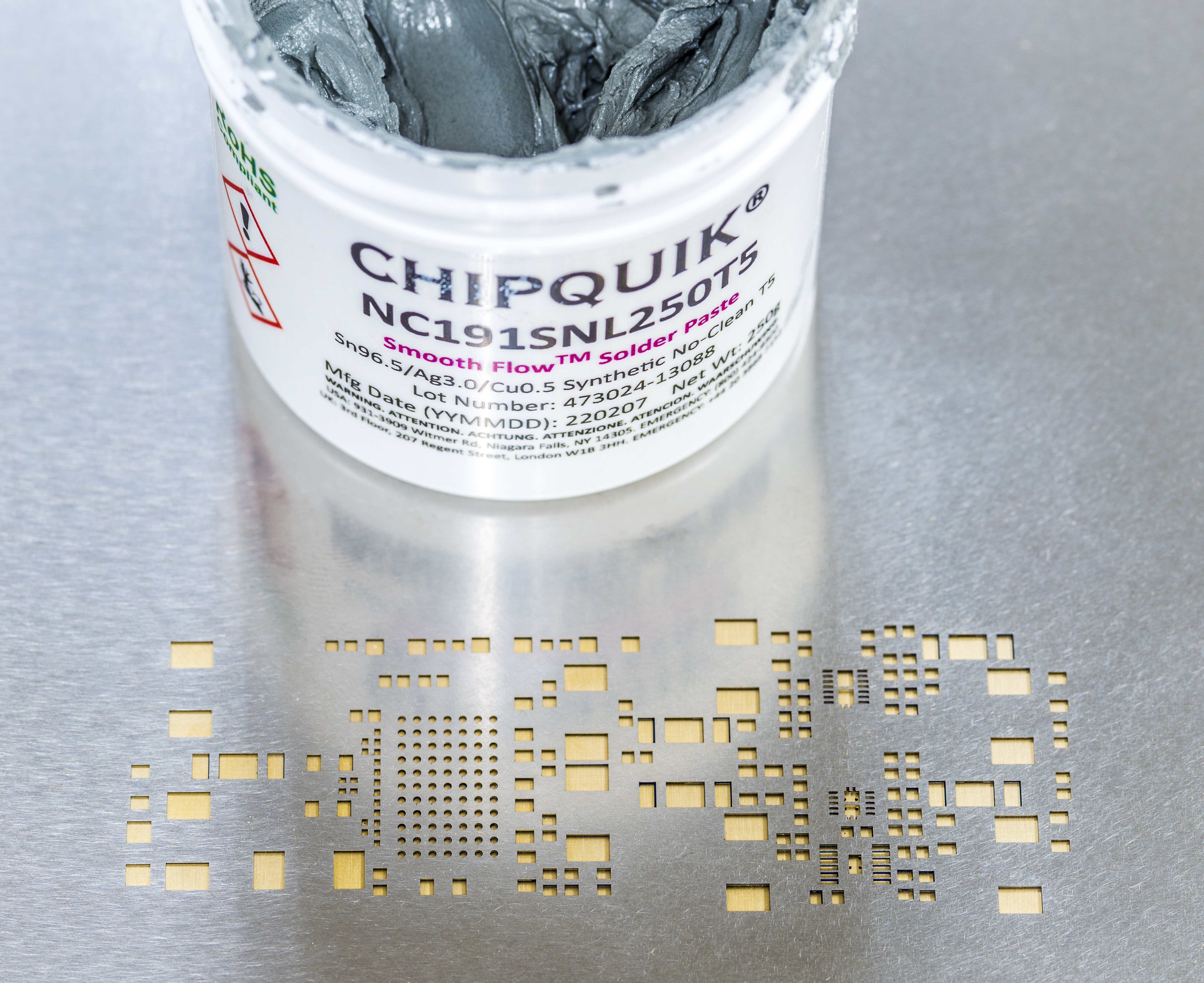
Here Chipquik® NC191SNL250T5 solder paste is used. This paste is lead-free type, with Sn95.6/Ag3.0/Cu0.5 solder. Working reflow temperature is around typical +217 °C similar to other RoHS pastes and solders. Paste is applied with a metal squeegee, but one can use also old credit card with just as good results. After application very carefully lift stencil straight up and check all printed paste on PCB pads. Everything should be aligned within half a pitch of finest component on the board. Paste amount should be uniform on all pads and there should be no missing/open spots.
One can see that bottom right corner with C4 pad did not get enough paste in our case. But I was not going to populate that capacitor anyway and decided to go ahead with placement anyway. Most critical pasted pads here are BGA footprint for LTM8049, DFN footprint for LT3094 and MSSOP footprint for LT3045MSE. There is a bit excessive paste on MSSOP, but should be alright to try.
Placement
Because I’m just building few prototypes here for lab use and not running thousand PCBA per day production I will place all components by hand with pair of steady tweezers. It is mundane but necessary work, where most of time is wasted by looking for right part, rotating it in proper orientation (remember pin 1 marks!) and gently dropping part on top of pasted pads in correct location. Make sure you have comfortable room for hand placement, as you cannot put a hand on top of the PCB with already placed (or not placed, but pasted!) area.
Good idea to start placement from smallest components while you have PCB surfaces still flat and accessible. Once large components are placed you’d have way less freedom of movement for tweezers around them. Largest parts and critical parts, such as fine-pitch BGAs or TSSOPs usually placed last, to avoid their accidental movement or misalignment.
BGA placement
BGA part placement is little tricky because you cannot see how balls on package match and align with pasted pads on PCB. But it’s possible to eyeball it to be close to center. Having good silkscreen with BGA parts outline also helps, but silkscreen can be shifted or mismatched relative to metal copper layers, so it’s only an approximate anyway.
Remember, BGA parts don’t need to be 100% precisely aligned to pasted pads because surface tension of molten solder during reflow will auto-correct the alignment automagically anyway. It only must have better than half-a-pitch alignment to pads, so BGA would not self-align itself to wrong row/column. Also assembling new PCBA is easier then repairing old one with BGA, because for new components and new PCBs you have nice and even surfaces and no oxidation on either of metal surfaces. One can find plenty of BGA assembly and repair videos on YouTube as well, for more ideas about how this process works in general.
Now next step, soldering or “reflow”
Reflow is a process where all components, PCB and solder paste will be heated to temperatures (usually +183 °C for leaded solder paste or +217 °C for lead-free) when solder balls in paste would melt and combine together into solid flowing blob and wet both component metal pins and PCB pads. During reflow initial stage flux will be activated and aid good wetting for all metal surfaces and also protect the joints from open air and oxygen access.

It is important to have correct temperature profile (not too cold and not too hot!) so flux, solder and components/PCB are all happy and doing it’s work as designed. Too low temperatures would render in excessive paste and cold joints and too high temperatures would burn flux away and damage PCB and/or components. Recommended temperature profile can be found in paste and most of active component datasheets and technical documentation.

PCBs inside oven conveyor going thru reflow process.
BGA balls look slightly squashed just as they designed to be on correctly assembled board. There are few tricks how to check large scale BGA packages assembly quality without typical in production environment X-ray imaging. One of the simpler things is optical inspection on each side with point light source in opposition. If there are no solder bridges between balls you should be able to see light shining from the other side of the package under microscope. Another bit more tedious way is to take fine wire, such as used in transformers and try to thread it between BGA ball rows and columns thru whole chip. If there is no excessive flux buildup under BGA wire should go thru relatively easy.

But with this large 1.27mm pitch and overall solder quality of resulting board it looks like BGA soldering was a success from first try. MSSOP and DFN packages have no shorts and look alright too.
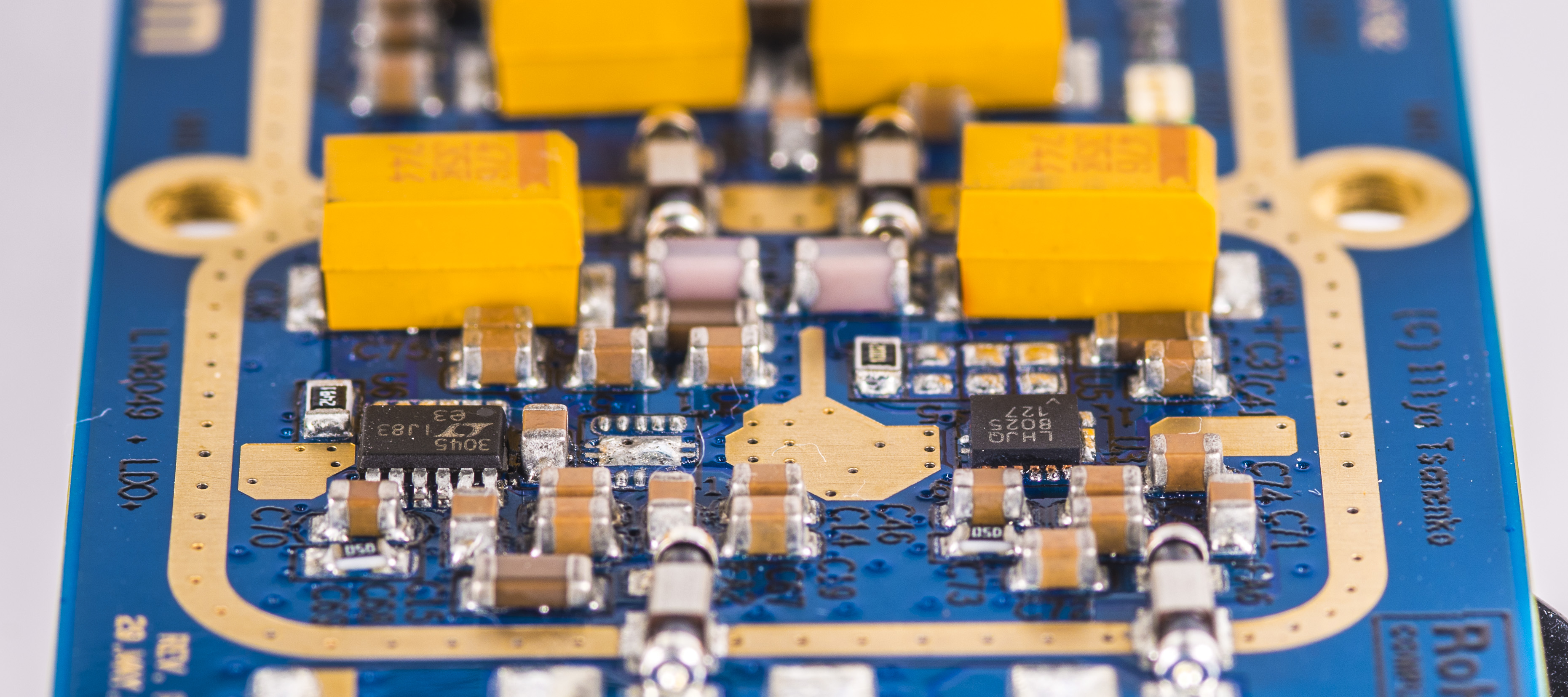
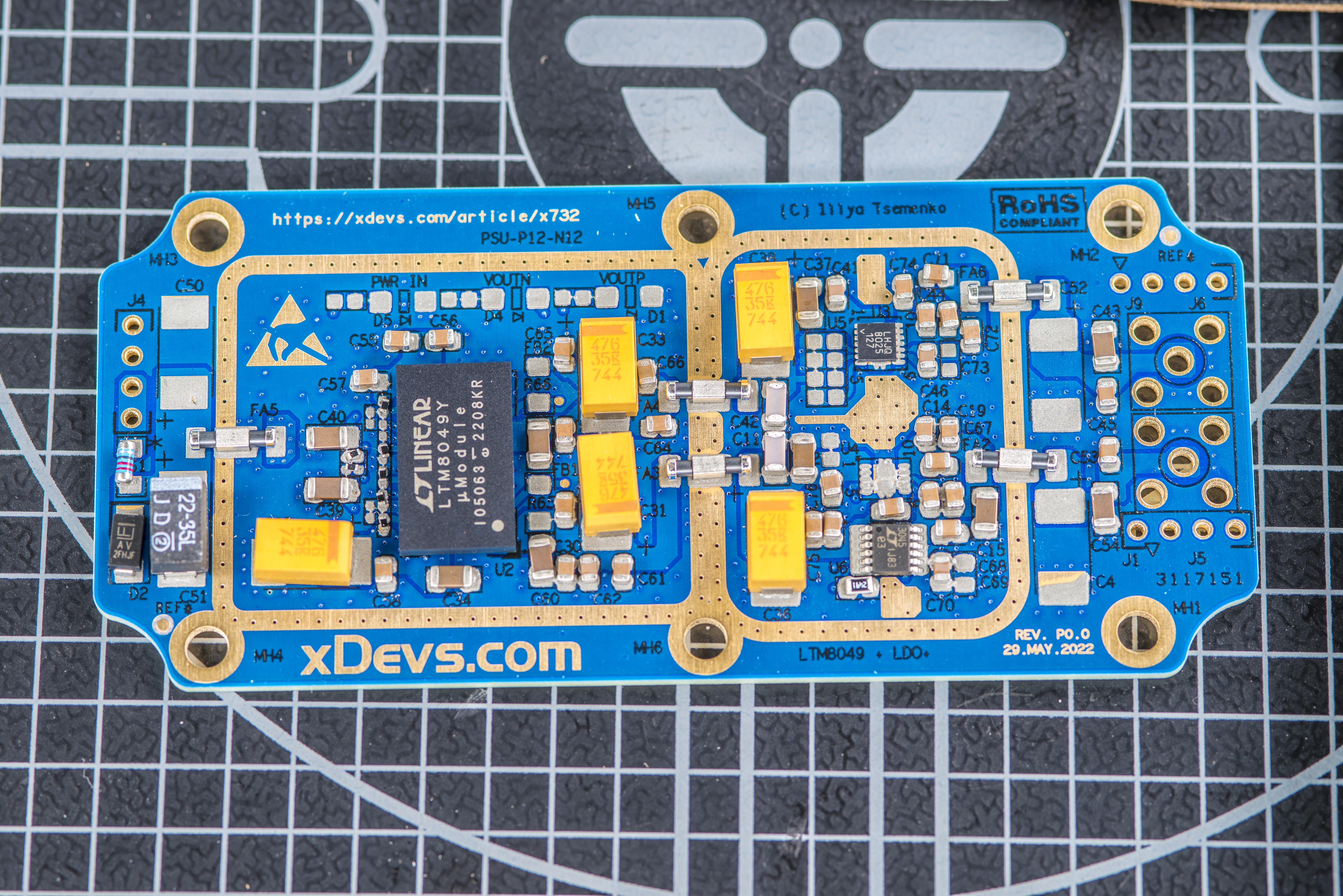
Finished board before power up:
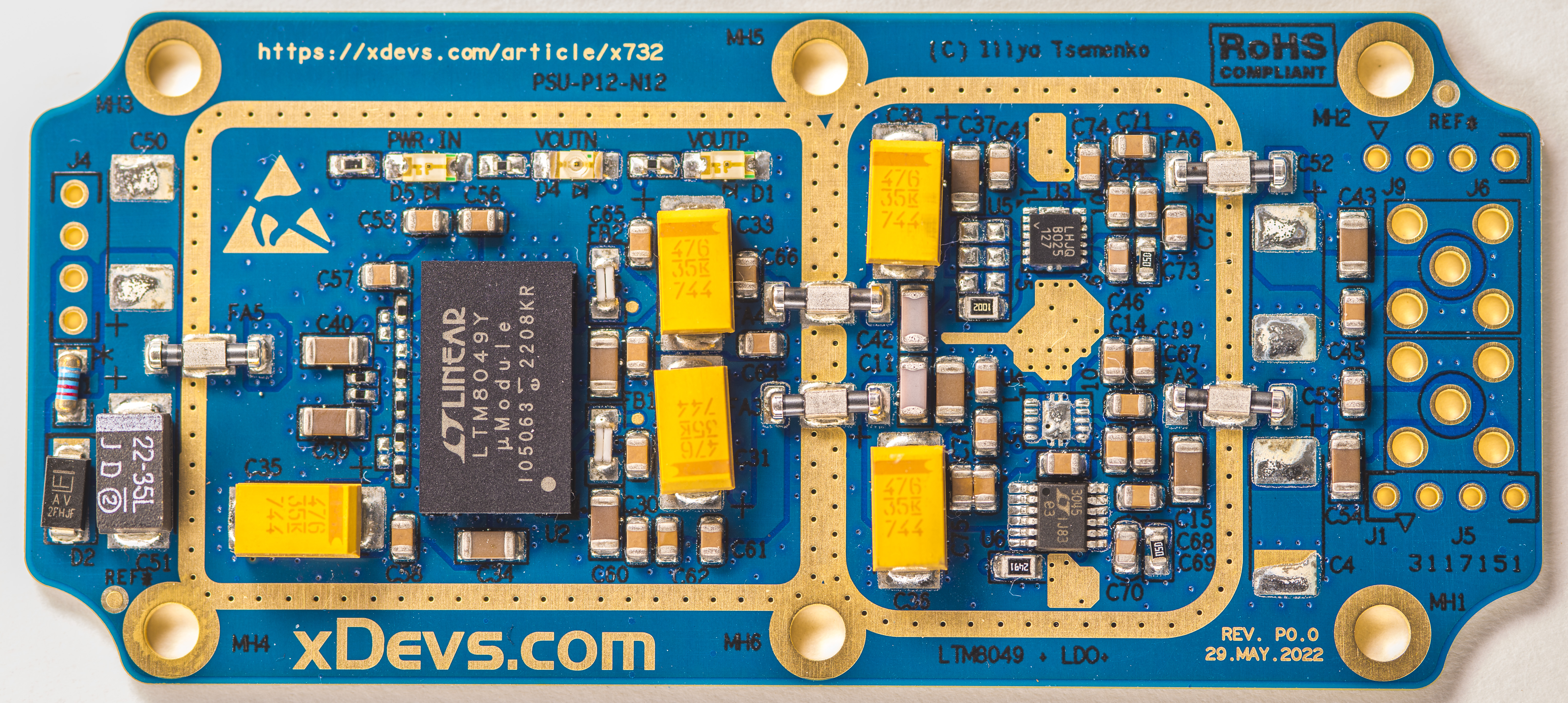
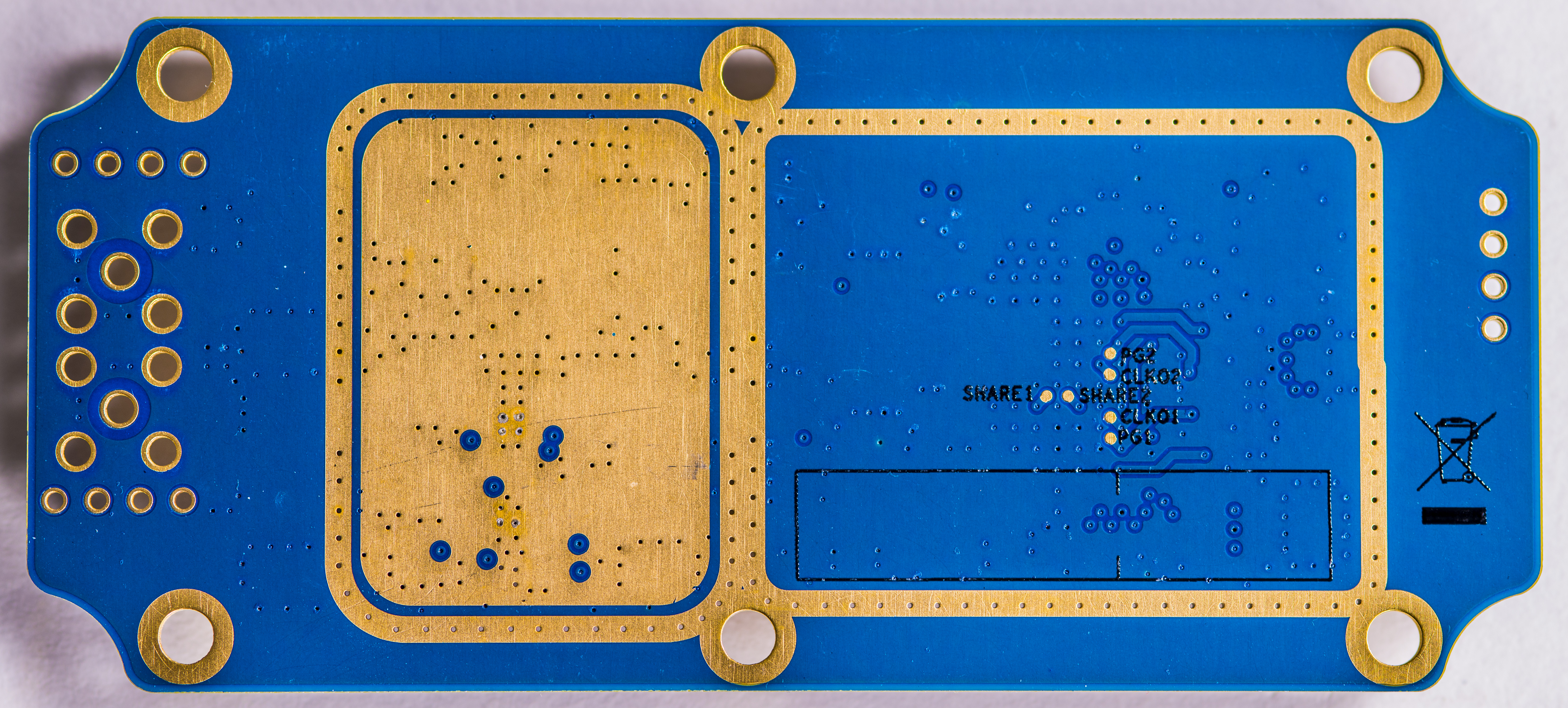
Back surface does not have any components and there is minimal solder leakage thru thermal vias under LT3045 and LT3094 regulators.
Short video showcasing the assembly steps as they listed in this work-log
This tutorial on assembly should help with anyone attempting to build simple prototypes but was afraid to do so until now.
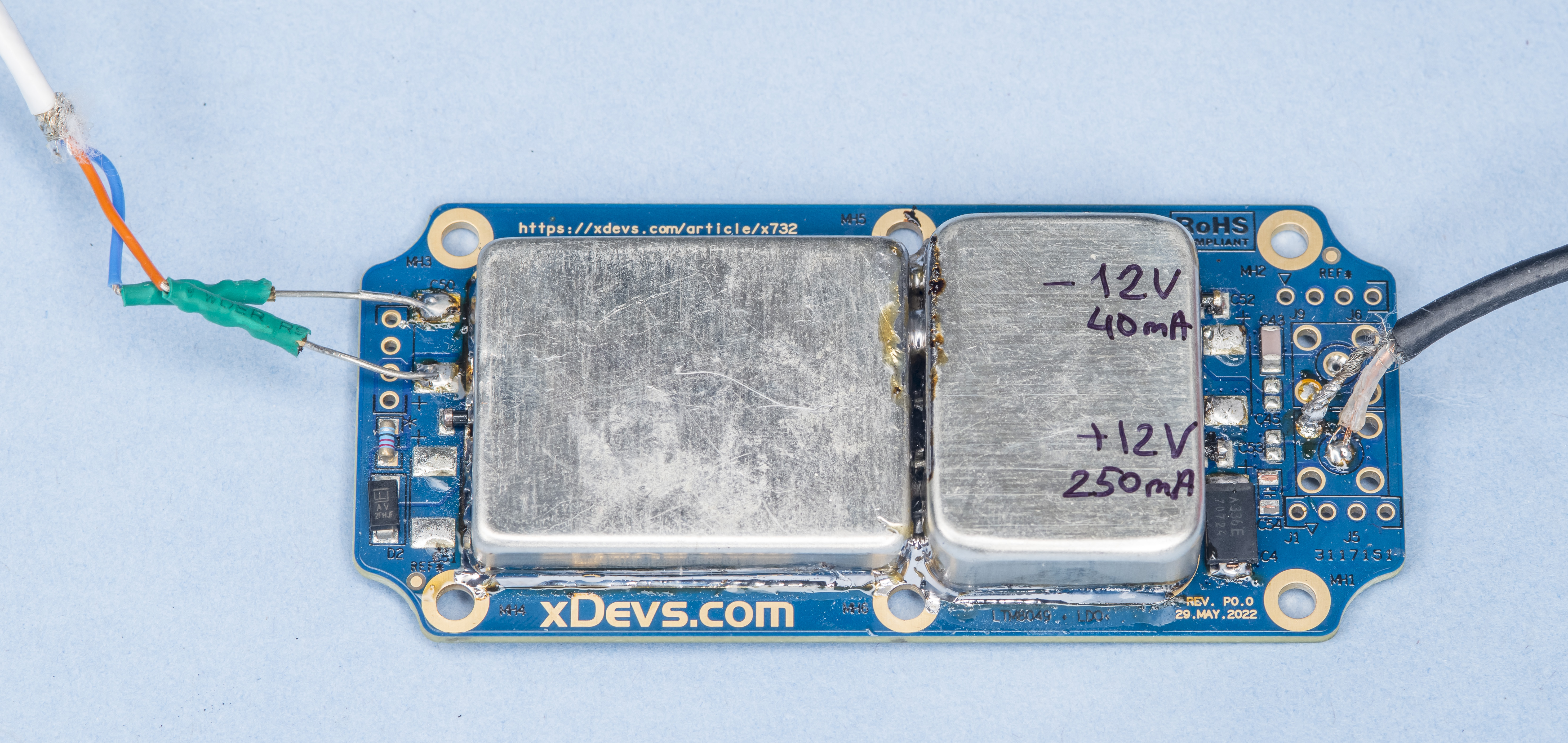
And finally the working module test prototype with shield cans mounted on.
LX reference
Total components list and BOM
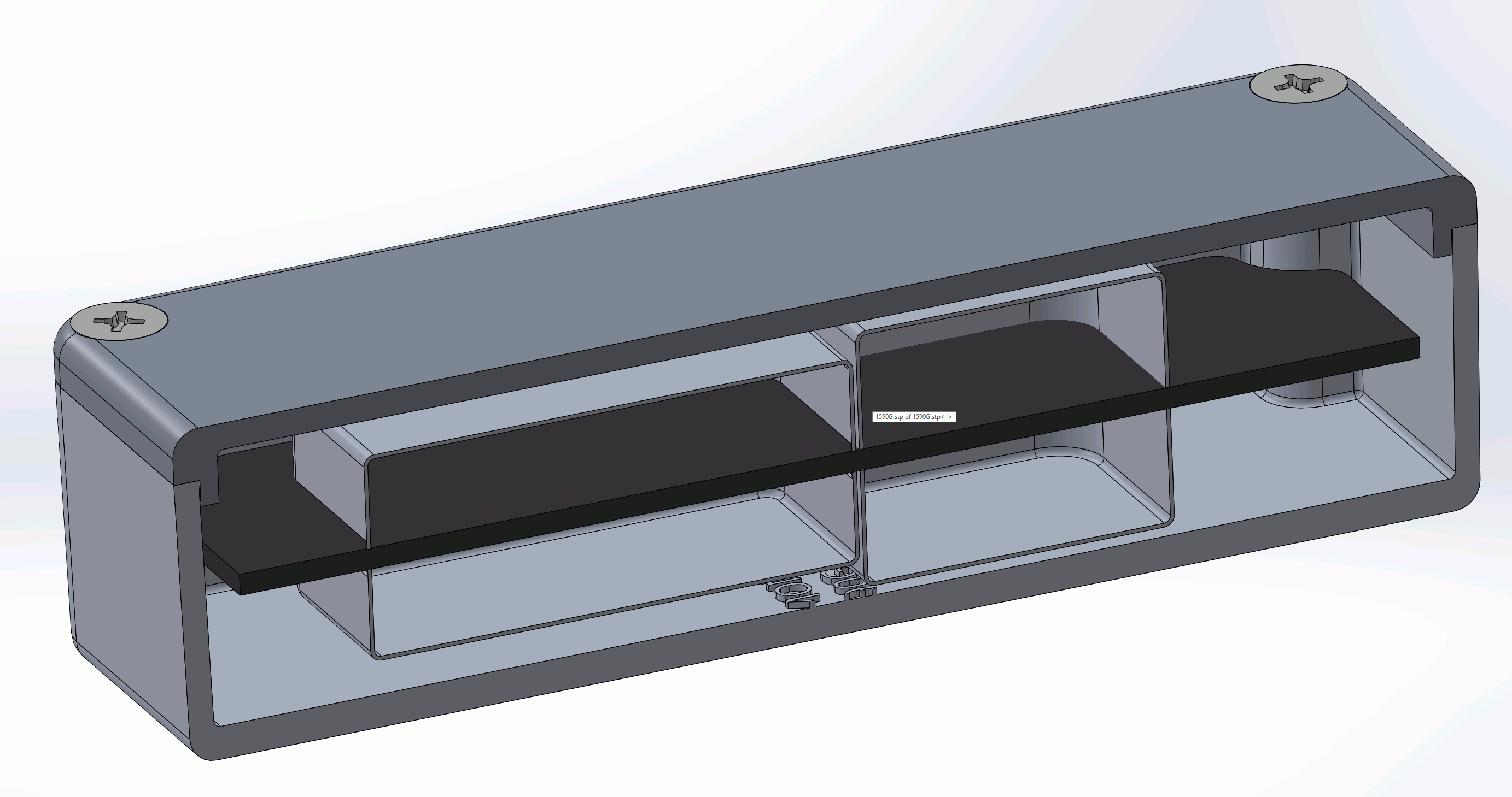
1590 case https://www.digikey.com/en/products/detail/hammond-manufacturing/1590G/409858
tinned steel shields https://www.digikey.com/en/products/detail/masach-tech-ltd/MS323-30S/13166522
tinned steel shields https://www.digikey.com/en/products/detail/masach-tech-ltd/MS375-10S/13166554
resistors
capacitors?
TVS?
M3 standoff https://www.digikey.com/en/products/detail/w%C3%BCrth-elektronik/970100321/6174761
Costs and summary
Projects like this are born from passion and a desire to share how things work. Education is the foundation of a healthy society - especially important in today's volatile world. xDevs began as a personal project notepad in Kherson, Ukraine back in 2008 and has grown with support of passionate readers just like you. There are no (and never will be) any ads, sponsors or shareholders behind xDevs.com, just a commitment to inspire and help learning. If you are in a position to help others like us, please consider supporting xDevs.com’s home-country Ukraine in its defense of freedom to speak, freedom to live in peace and freedom to choose their way. You can use official site to support Ukraine – United24 or Help99. Every cent counts.
Modified: Feb. 4, 2026, 1:17 a.m.