Contents
- Intro
- Disclaimer
- Manuals
- Configuration
- Overview
- Digital board module
- Power supply assembly
- HP GNDU/ADC module
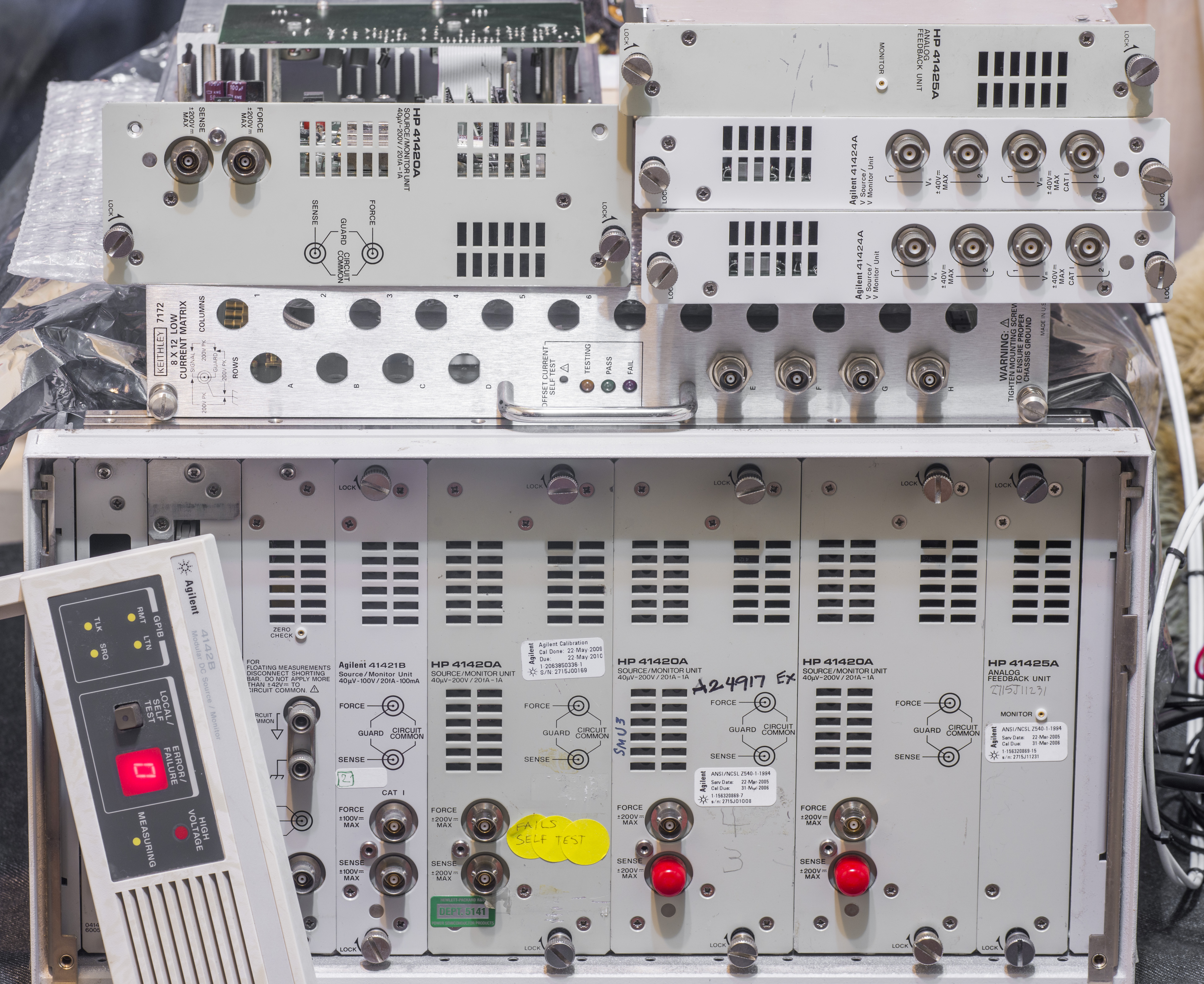
- HP 41420A HPSMU High-power Source/Monitor 200V/1A Unit
- HP 41421A MPSMU Medium-power Source/Monitor 100V/100mA Unit
- HP 41422A HCU High-current Source/Monitor 10V/10A Unit
- HP 41423A HVU High-voltage Source/Monitor 1000V/10mA Unit
- HP 41424A V source/V Monitor Unit
- HP 41425A Analog Feedback Unit
- Repair
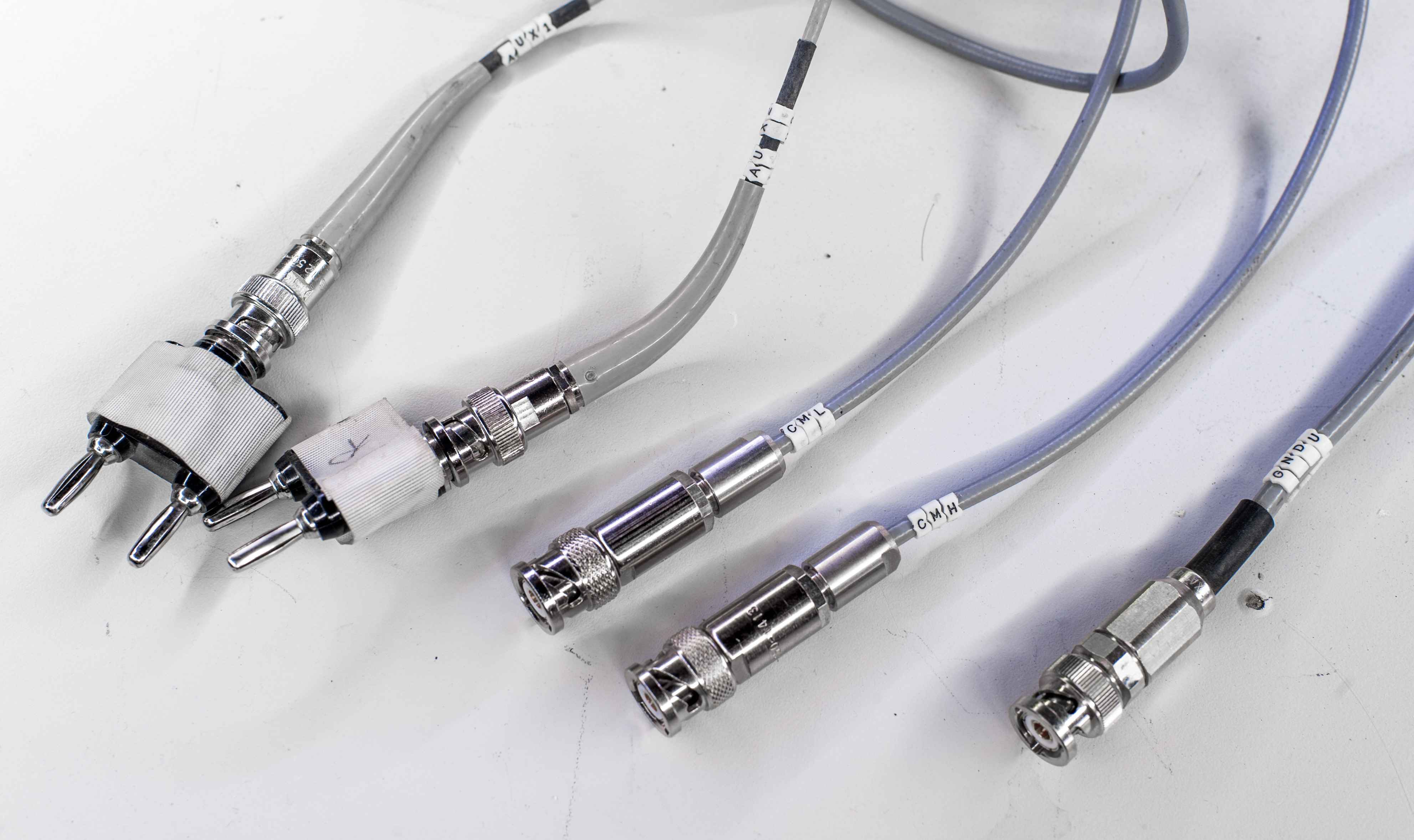
- HP 4085-61684 triax cable assembly from HP 4062UX system
- Firmware
- Testing
- Summary
Intro
Most of electronics design engineers use many datasheets and component application notes every day. Most of these people trust information in manufacturer datasheets and usually do not spend much time checking and testing if actual component comply with what is in the datasheet. To be fair, most of the time data and ratings presented in datasheets are correct. But just like with anything else made by people, sometimes there are errors and mistakes. How are those datasheet values were measured, what was measurement error level, and how those nice plots were made? Given the amount of testing and validation that goes into any mass-produced electronics, automatic measurement and testing setups were used to do this testing quickly and reliably. High speed voltage and current sources, controlled by computer program were used to provide stimulus to part and dedicated measurement instruments were used to get results and plot nice graphs, we all can enjoy in specifications.
Of course this can be done to some extent using off the shelf sources and multimeters, linked in via GPIB to usual computer with proper software, but such a setup would not be very reliable for automated production line, which need to test thousands of components every hour. Also usual gear is not designed for extreme ranges of signals, such as very low currents (femtoamps and nanoamps!) or high voltages (hundred, sometimes thousands of volts). To do this testing special modular machines were designed, which can provide all required functionality in one compact package. They usually large, bulky, designed to fit into 19” racks and very expensive. Just a triaxial cable 1 meter long, which is required for these low-current measurements and noise performance alone can cost over $600 USD, and you will need dozen of them even for simple op-amp test.
In this article we will take a look on old HP/Agilent 4142B Modular DC Source/Monitor which is good example of such analyzer equipment. This model was discontinued on July 2003, and it’s obsolete from September 2008. Modern HPAK E5260A 8-slot high speed measurement mainframe and the E5270B 8-Slot precision measurement mainframe are code-compatible with the 4142B and they can replace the 4142B in most applications today. While E5260A and E5270B are nicer and have more features and better in specs, functionally all these units are same and targeted to same application – testing semiconductor devices. Alternative system, better suitable for research/benchtop use is Keysight B1500A, which also expandable up to eight SMU channels.
Also common competitor for these HP/Agilent/Keysight units is Keithley 4200-SCS system and Keithley 2600 series SMUs.
Unit main features and specifications:
- Modular architectures, up to 8 slots for 4142x series modules.
- Wide measurement range with high resolution
- Voltage ranges: ±4 µV to ±1000V, 0.05% accuracy (depend on module)
- Current ranges: ±20 fA to ±10A, 0.2% accuracy (depend on module)
- Pulse measurement 1ms to 50ms, 100µs resolution
MSRP for 4142B base unit was at $12100 USD decades ago, with modules price range from $1900 USD to $6500 USD for High-voltage SMU. Modern Keysight units even more expensive.
Disclaimer
Redistribution and use of this article or any files referenced in it, in source and binary forms, with or without modification, are permitted provided that the following conditions are met:
- Redistribution of article must retain the above copyright notice, this list of conditions, link to this page (https://xdevs.com/fix/a4142b/) and the following disclaimer.
- Redistribution of files in binary form must reproduce the above copyright notice, this list of conditions, link to this page (https://xdevs.com/fix/a4142b/), and the following disclaimer in the documentation and/or other materials provided with the distribution, for example Readme file.
All information posted here is hosted just for education purposes and provided AS IS. In no event shall the author, xDevs.com site, or any other 3rd party, including Keysight be liable for any special, direct, indirect, or consequential damages or any damages whatsoever resulting from loss of use, data or profits, whether in an action of contract, negligence or other action, arising out of or in connection with the use or performance of information published here.
If you willing to contribute or add your experience regarding any test instruments or provide any extra information, such as firmware dumps, internal photographs, you can do so following these simple instructions
Manuals
HP 4142B HP-IB Command reference
HP 4142B Operation manual with Plug-Ins info, Edition 5, March 1992
HP 4142B Control Software Programming Manual, Edition 1, Jun 1991
DC Characterization of Semiconductor Power Devices, Product Note 4142B-1
Simplification of DC characterization and analysis of Semiconductor Devices
High-speed DC characterization of Semiconductor Devices from Sub-pA to 1A
AN 356-1: Techniques & Applications for 4142B, August 1988
And most important document for service and maintenance:
HP 4142B Service Manual, February 1992
Thanks to KO4BB site!
Configuration
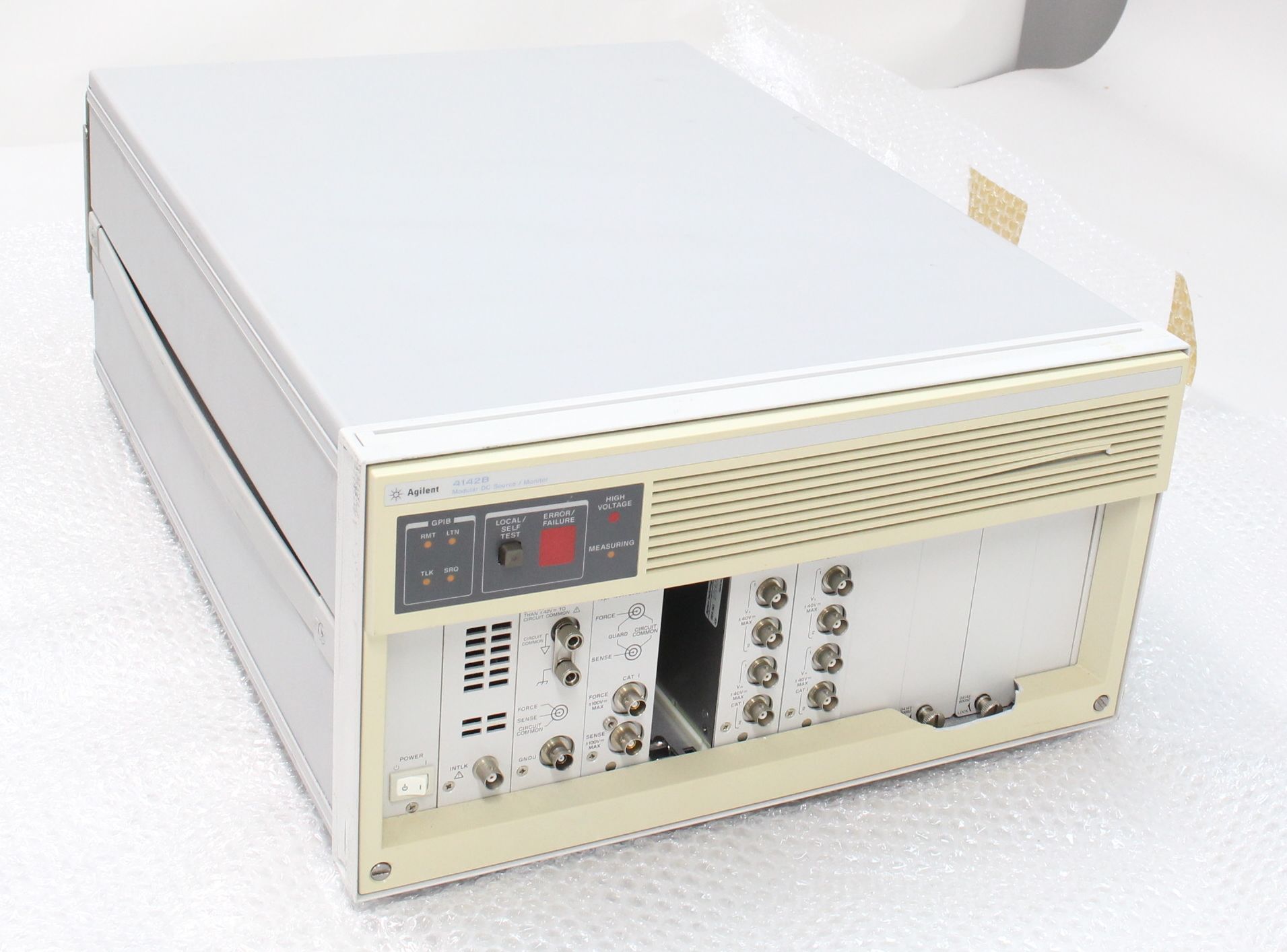
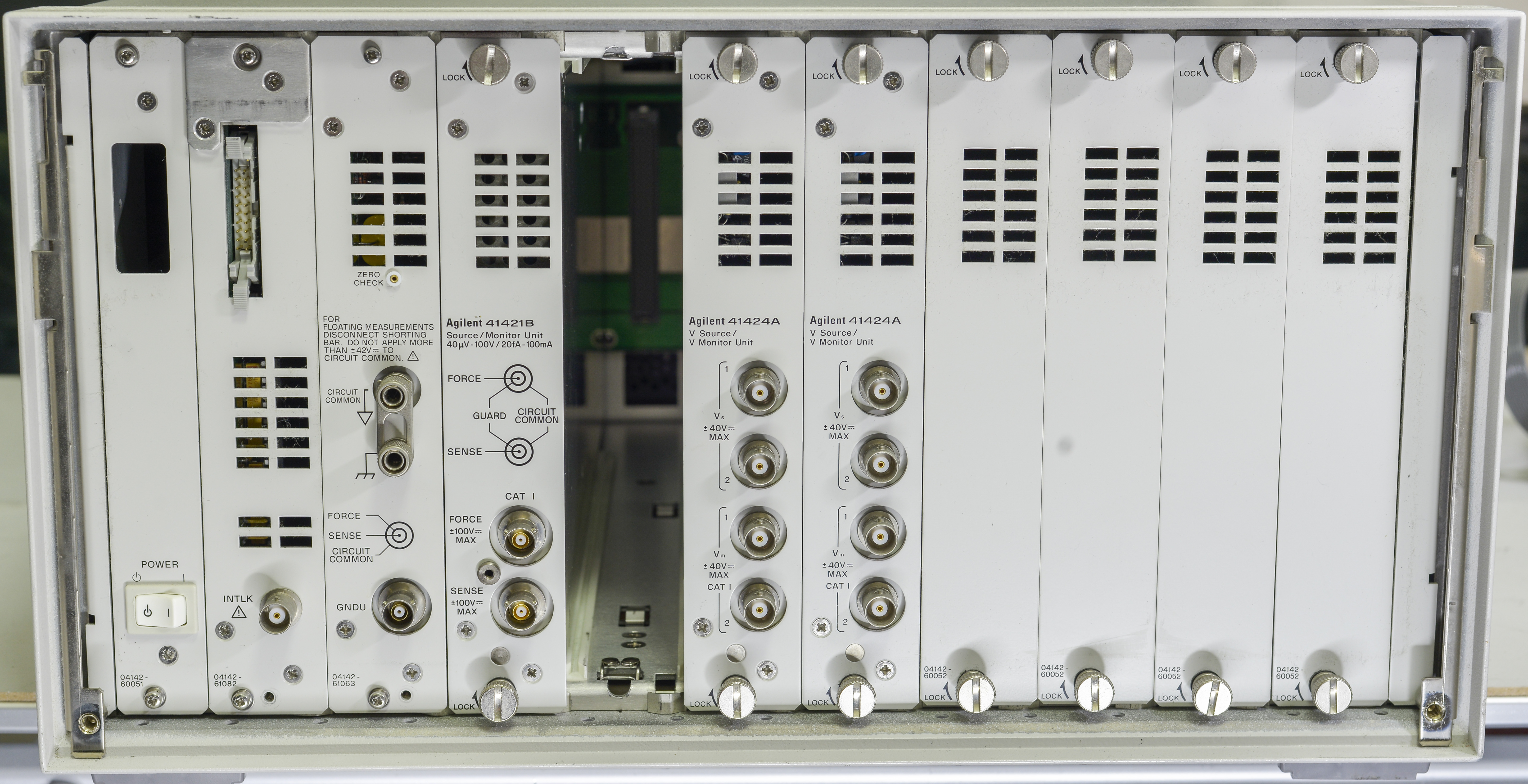
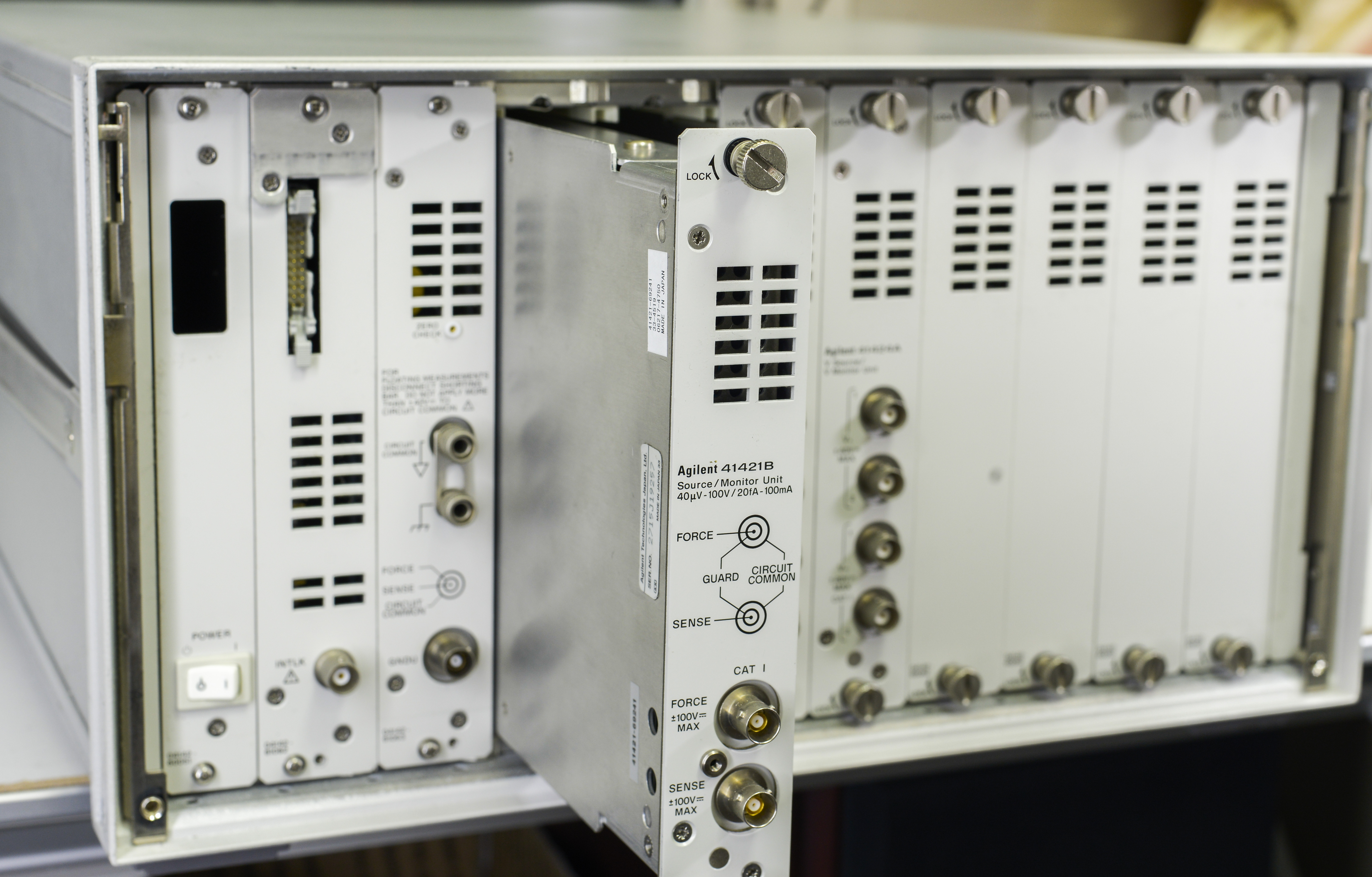
I’ve got unit with main modules, 1 × 41421B SMU and pair of 41424A voltage sources/monitors. There some minor cosmetic damages, such as front panel plastic yellowing, damaged bottom edge. These issues are not affecting operation.


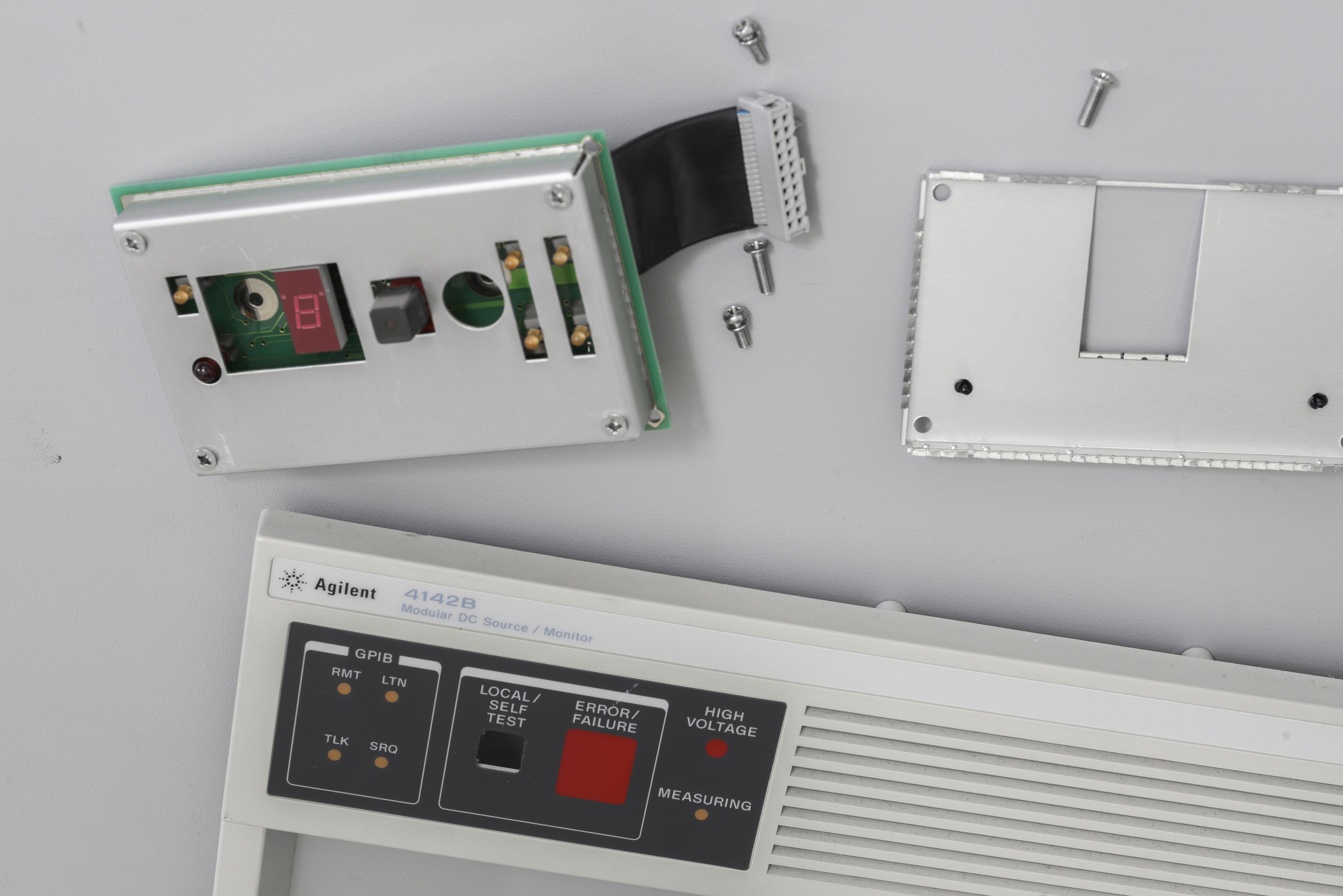
Front panel removal is quick and easy operation. It’s normal procedure required for installing/removal of mainframe modules. There is a hook latch on top corners to lock front panel cover securely in place.
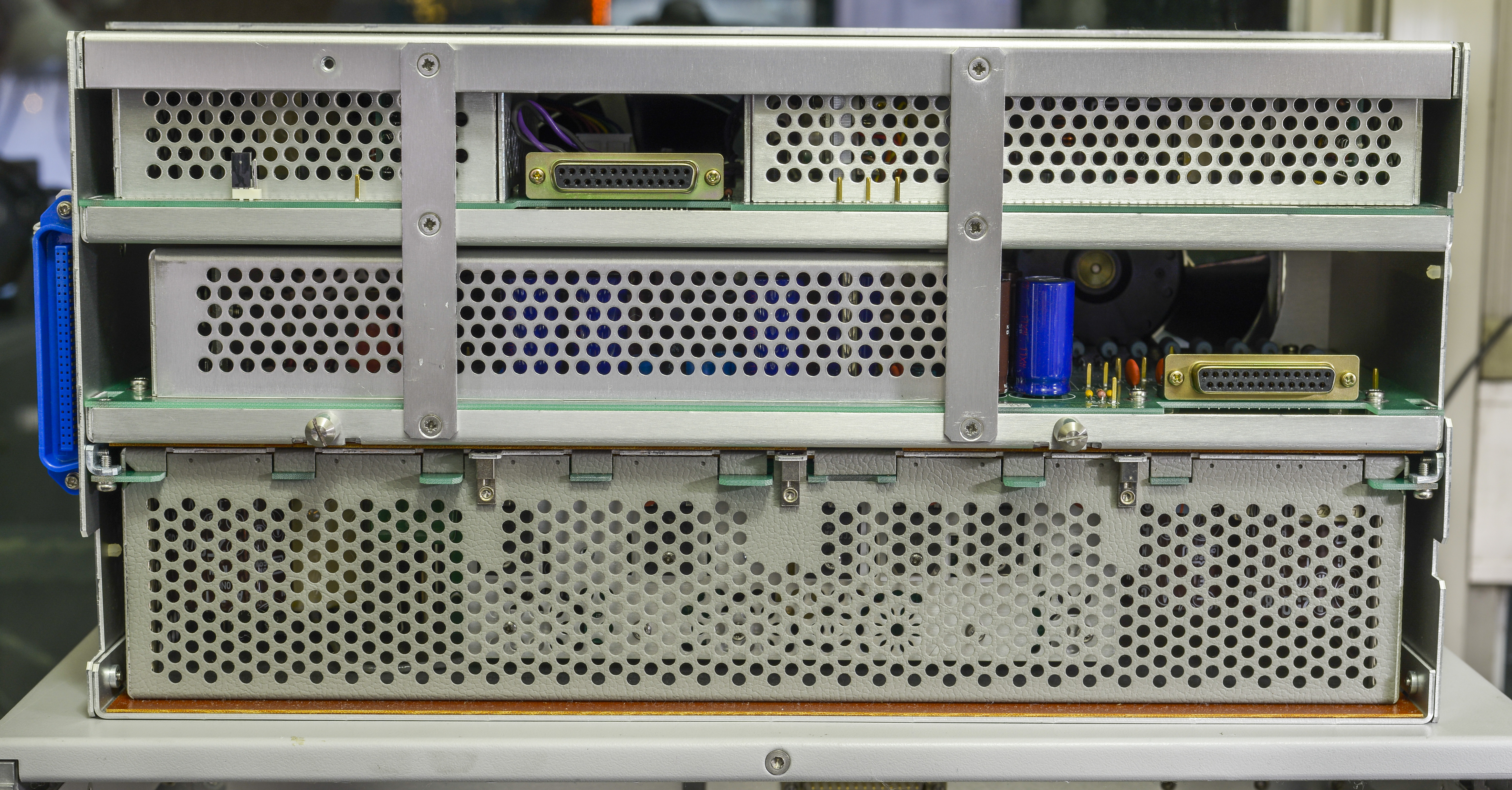
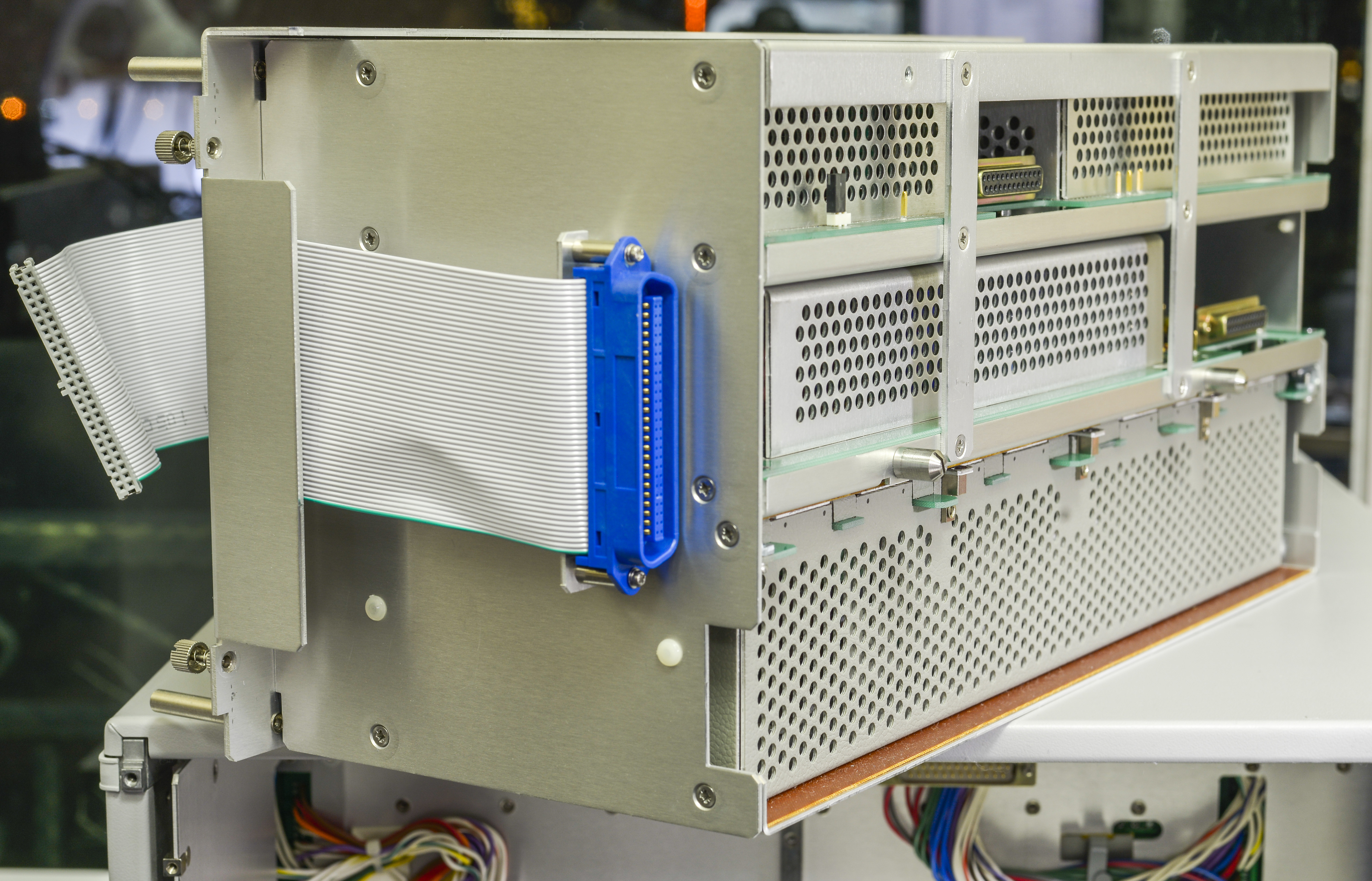
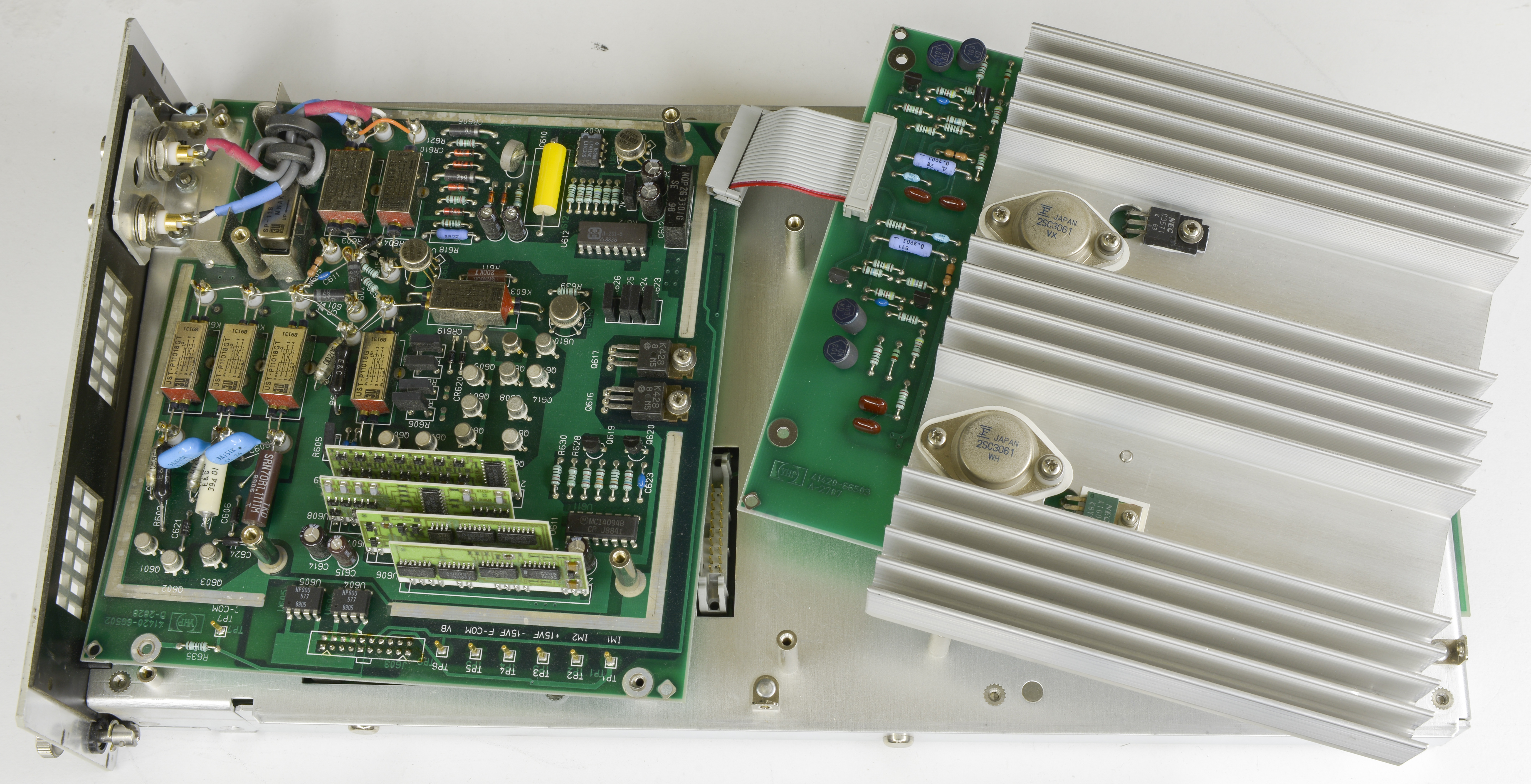
Here’s instrument without front panel cover. HP/Agilent 4142B minimum configuration – digital module 04142-61082 with processor and GNDU SMU 04142-61063 which acts as reference point for all sources and monitor units.

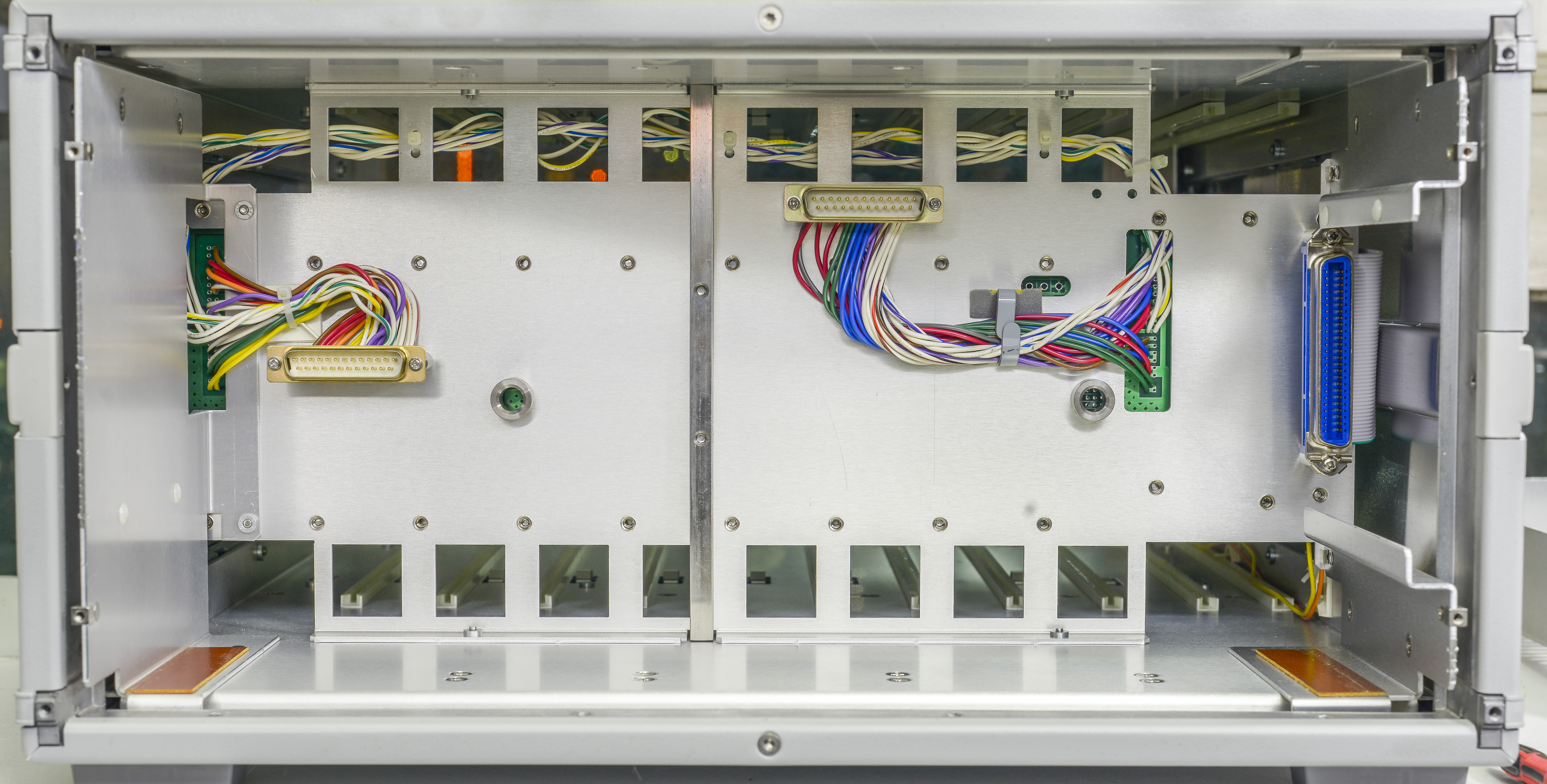
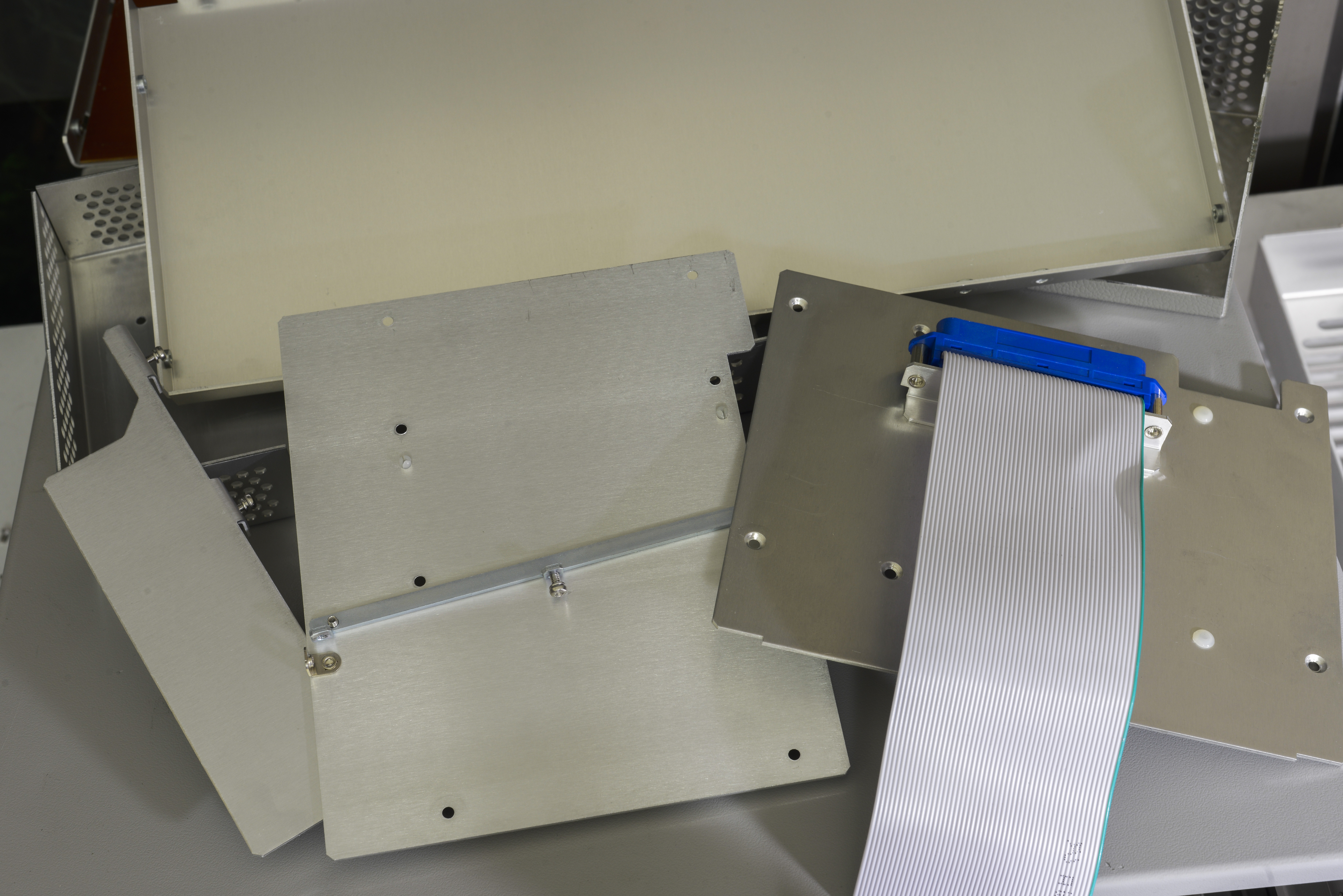
Mainframe with all modules removed.
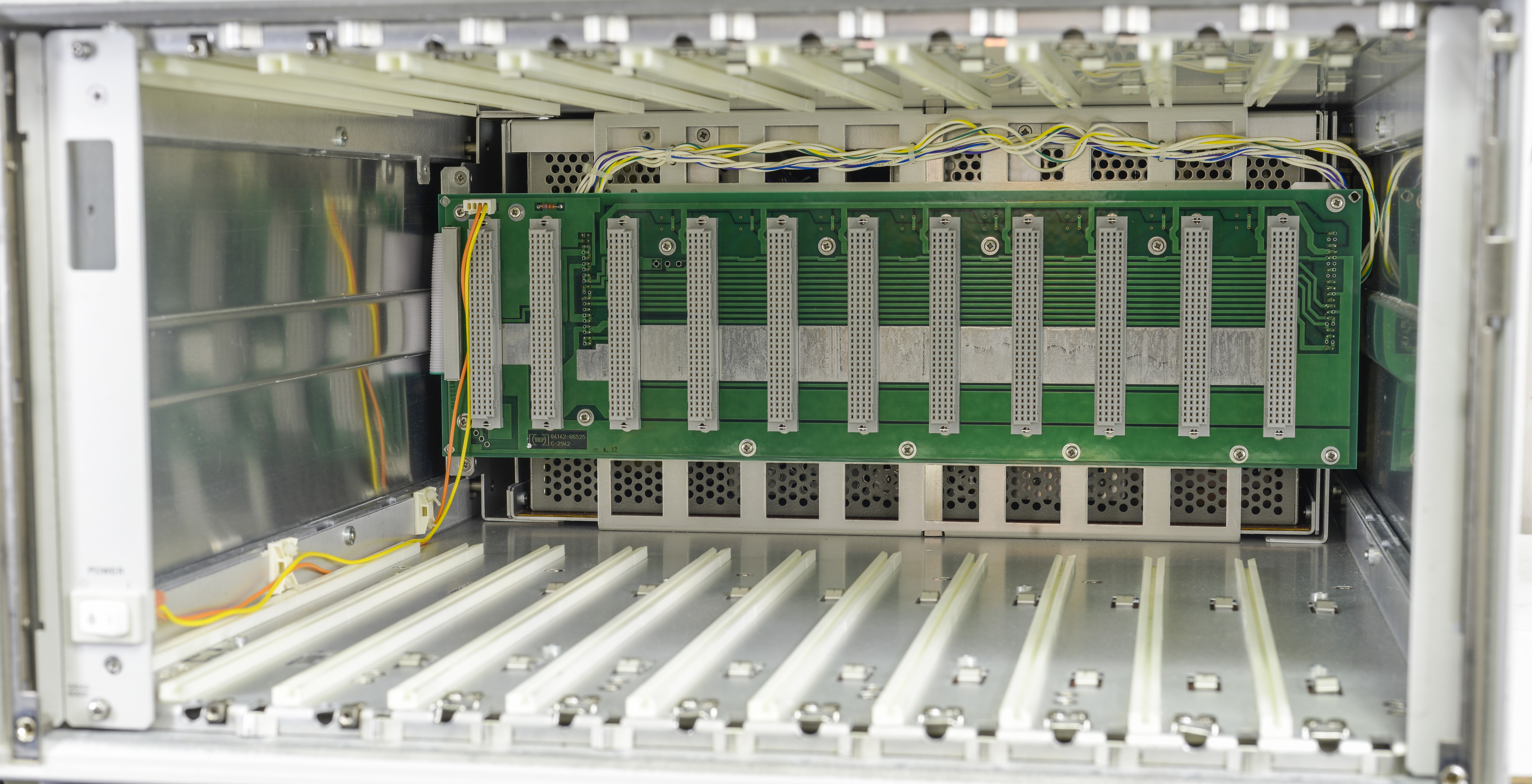
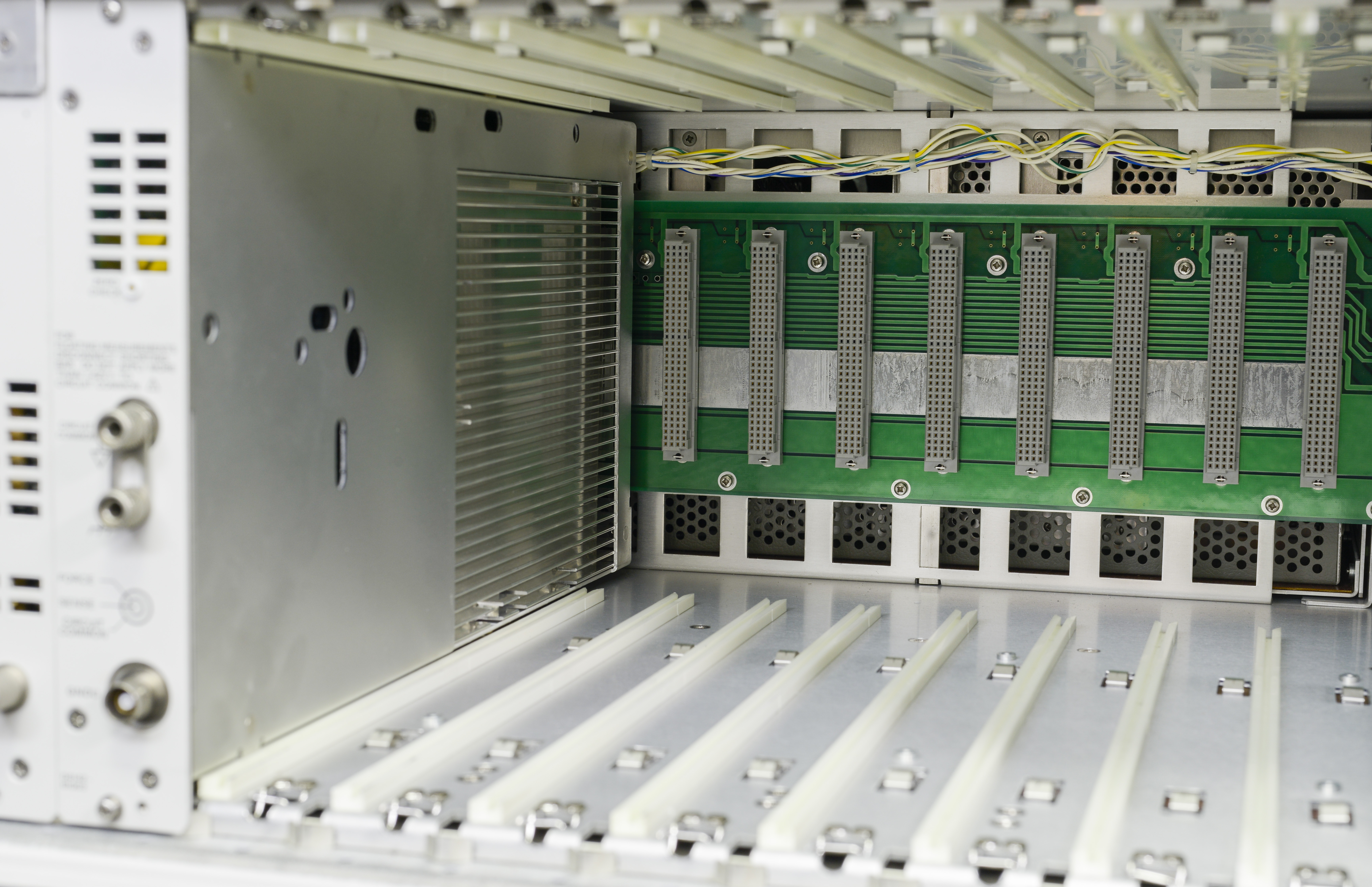
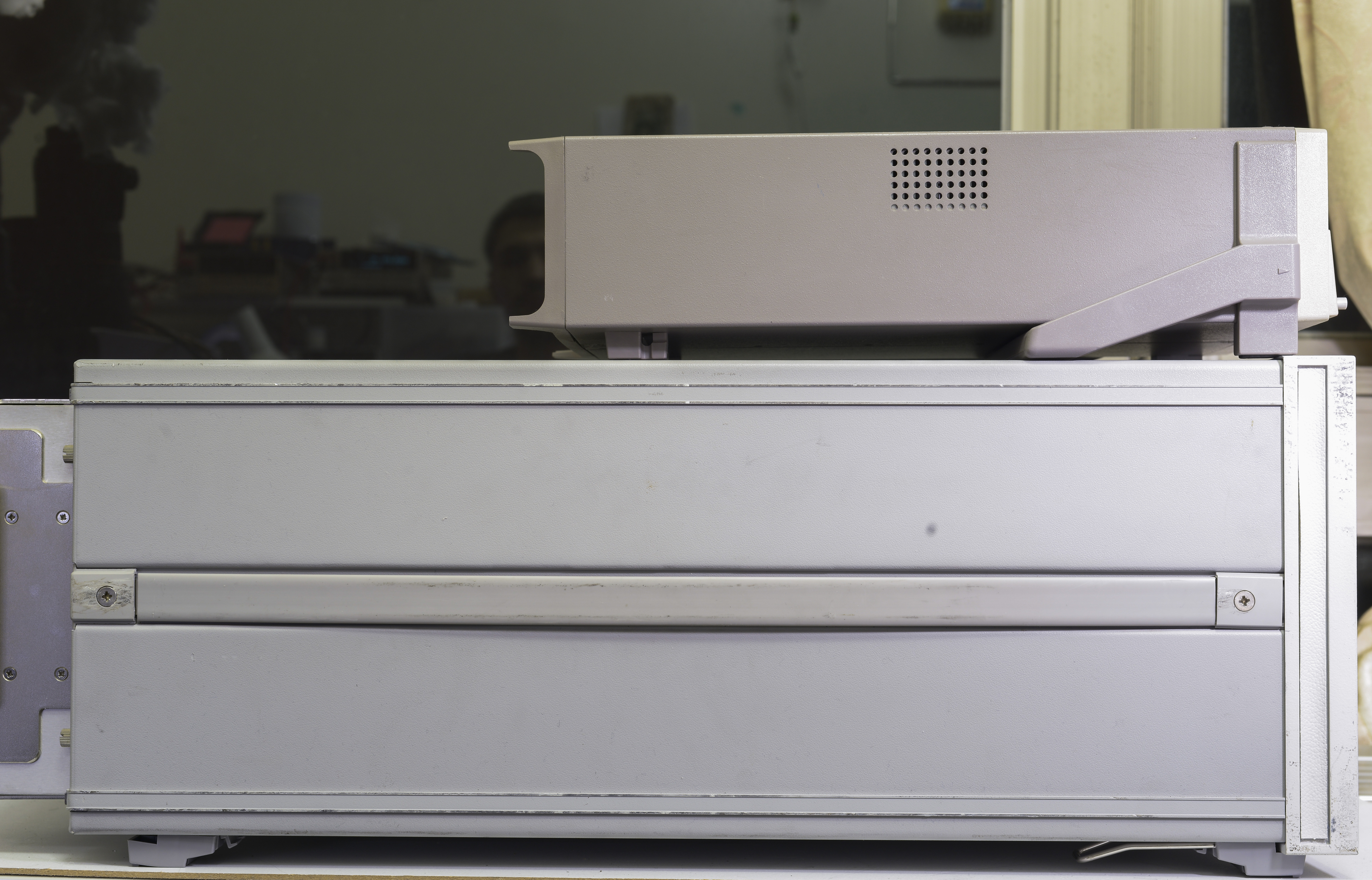
4142B is large bulku 4U 19” device. Here comparison of mainframe with system DMM such as Keithley 2001. Mainframe takes up to 8 modules, which can be placed in any slot. Some modules take 1 slot, and other ones may need up to 2 slots space.
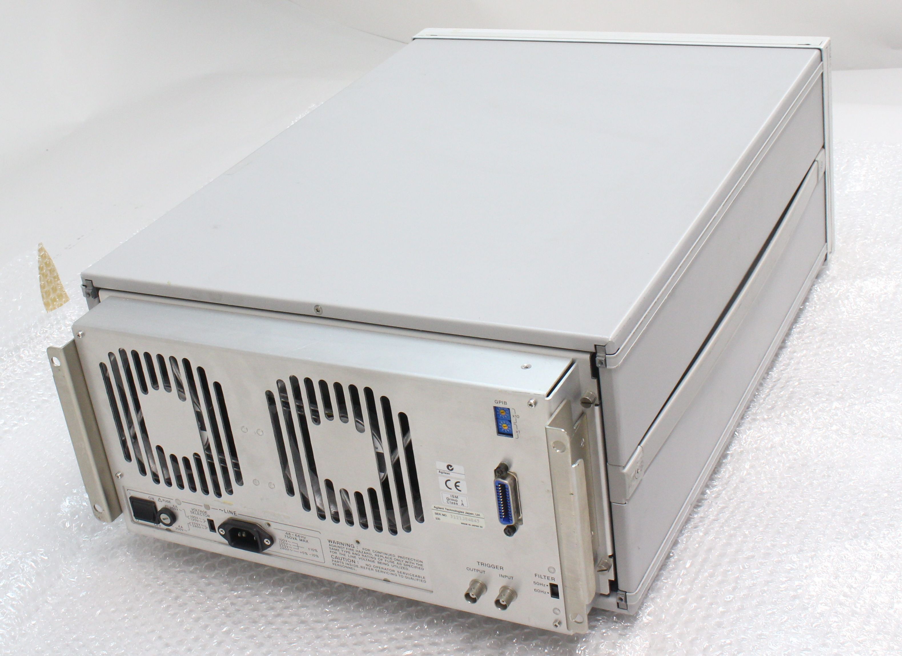
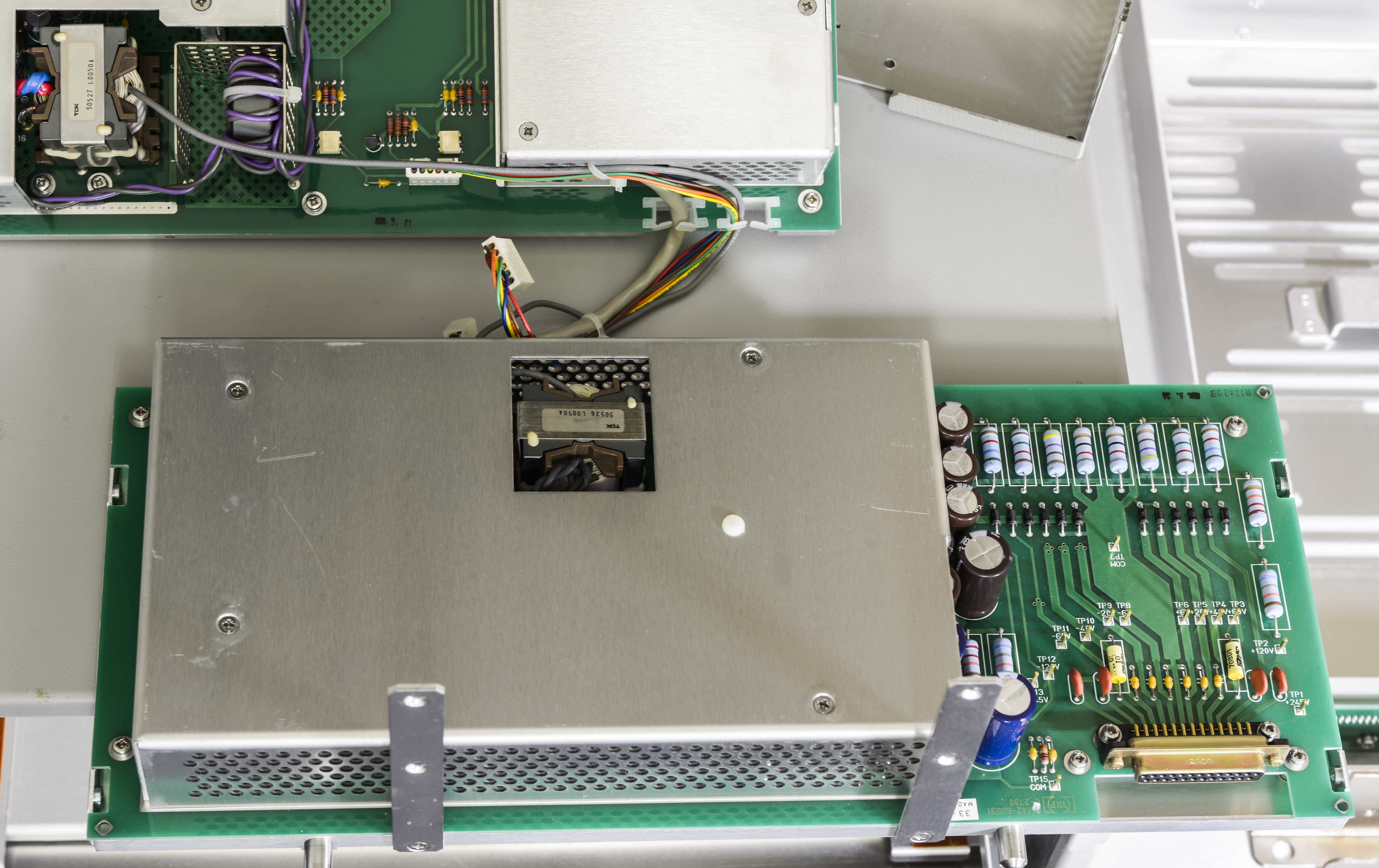
Rear panel have pair of 24V Sanyo Denki San Ace 120 × 38mm fans with metal frames. These fans are operating on constant speed and produce well noticeable noise.
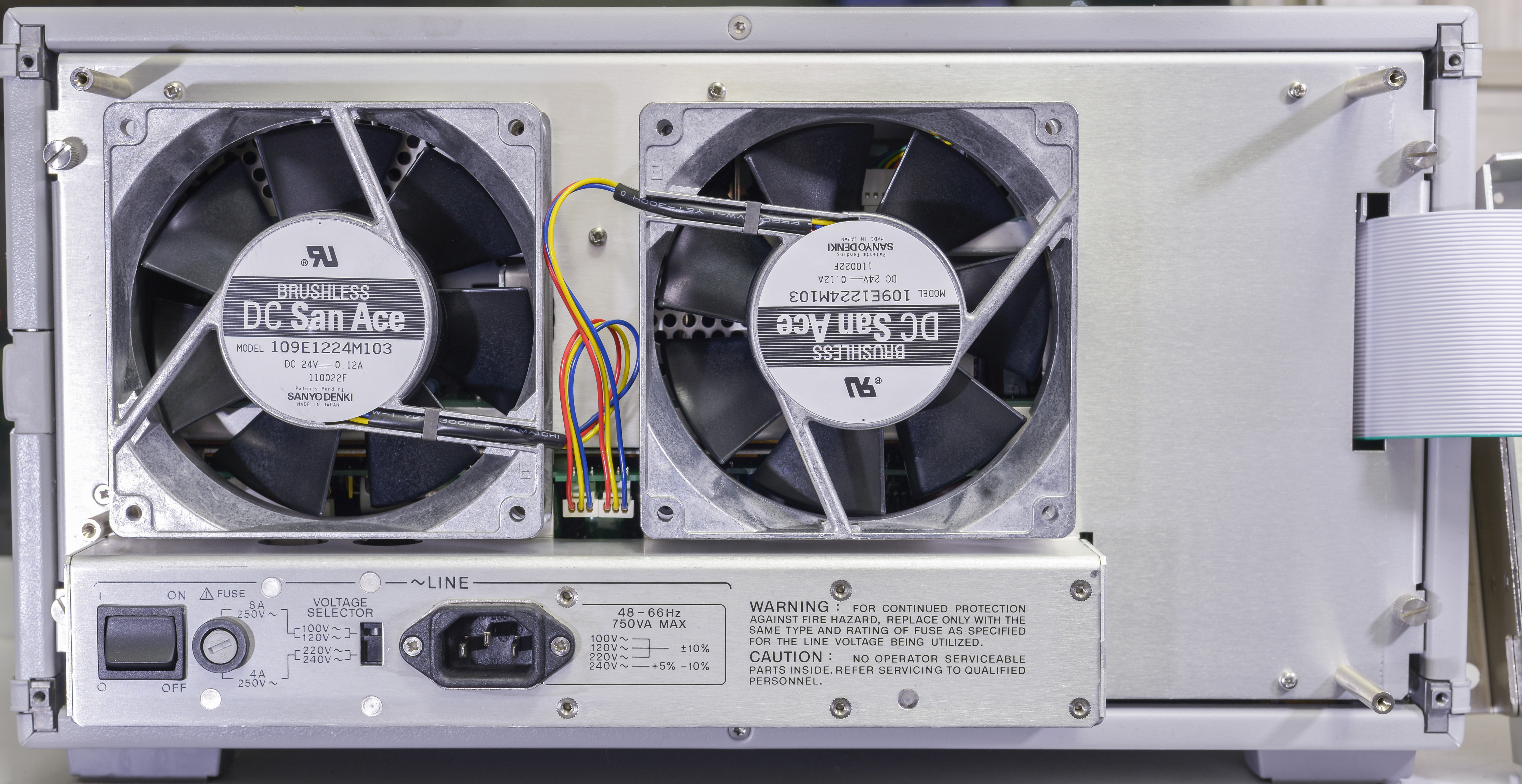
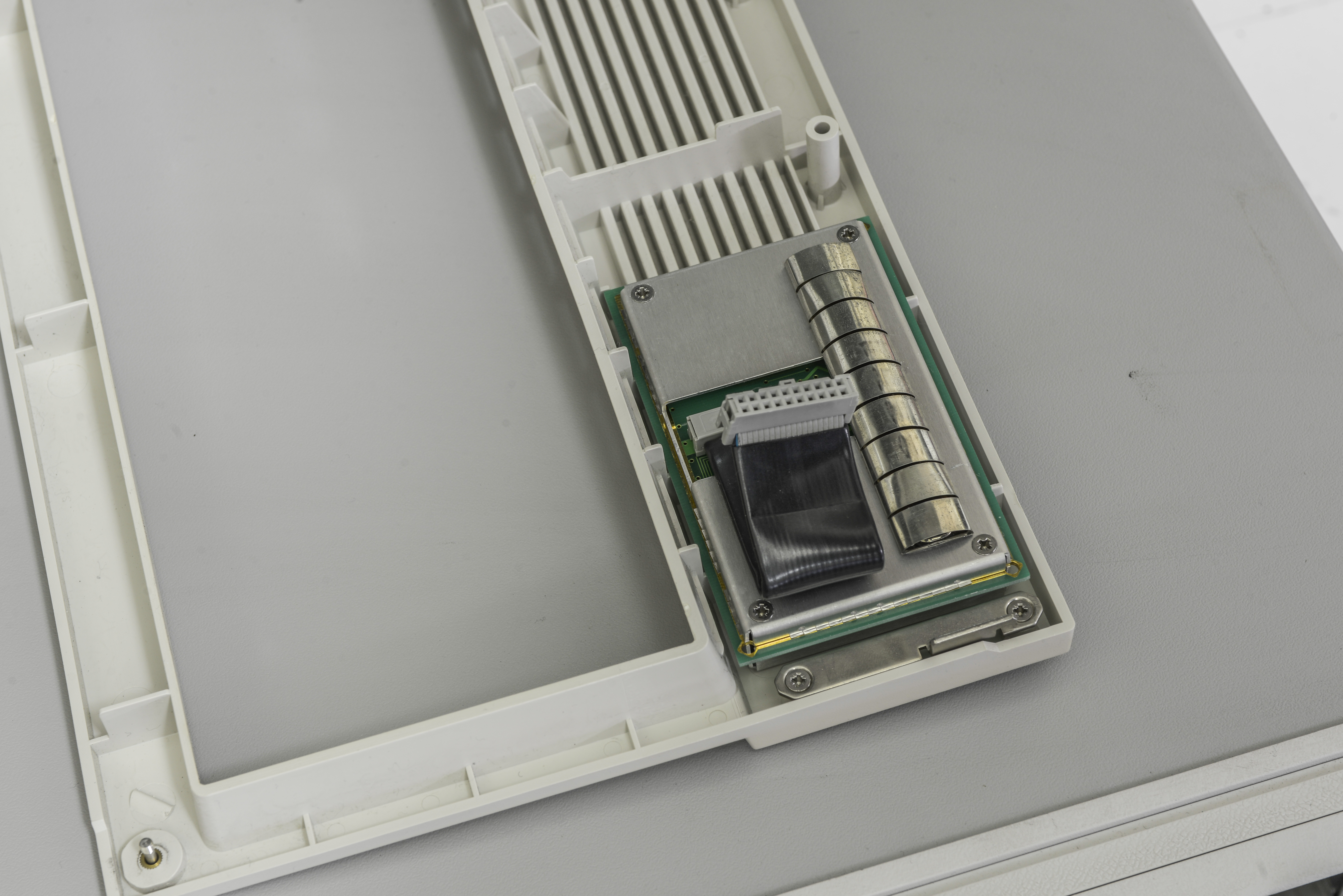
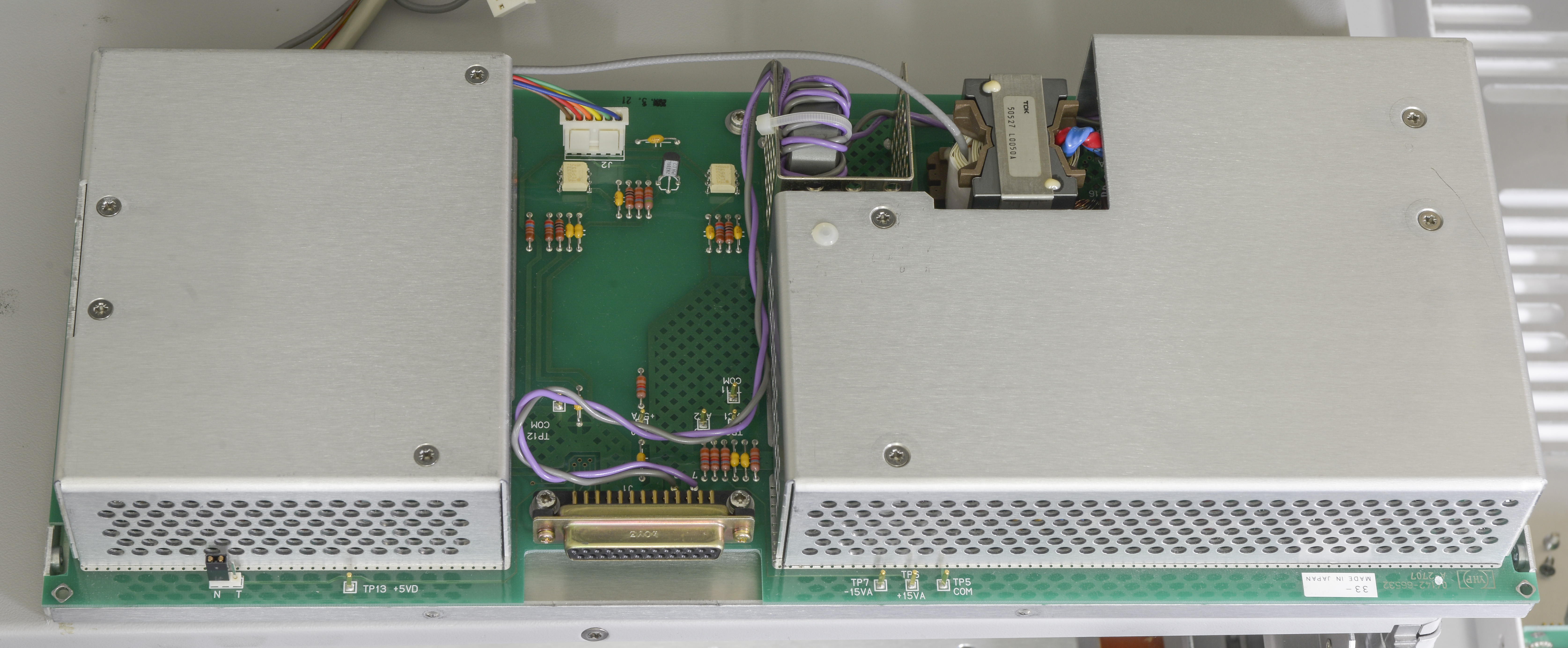
Fans are mounted directly on power supply’s cover, which is designed as assembly of three sub-modules. Whole assembly can be removed from the frame with just a screwdriver. This is done to reduce service time of the mainframe in case of PSU failures.
Overview
Here’s overall mainframe block diagram:

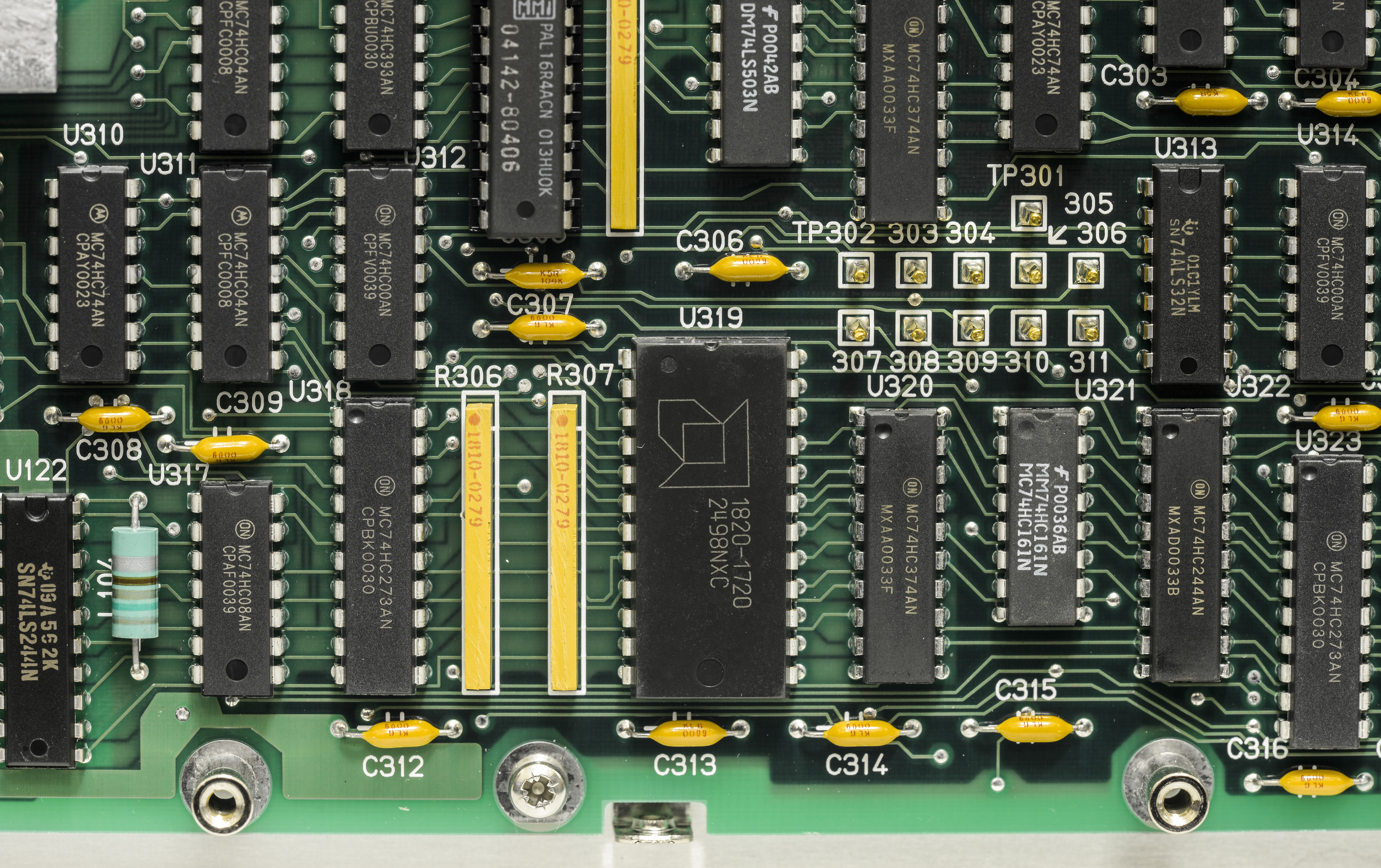
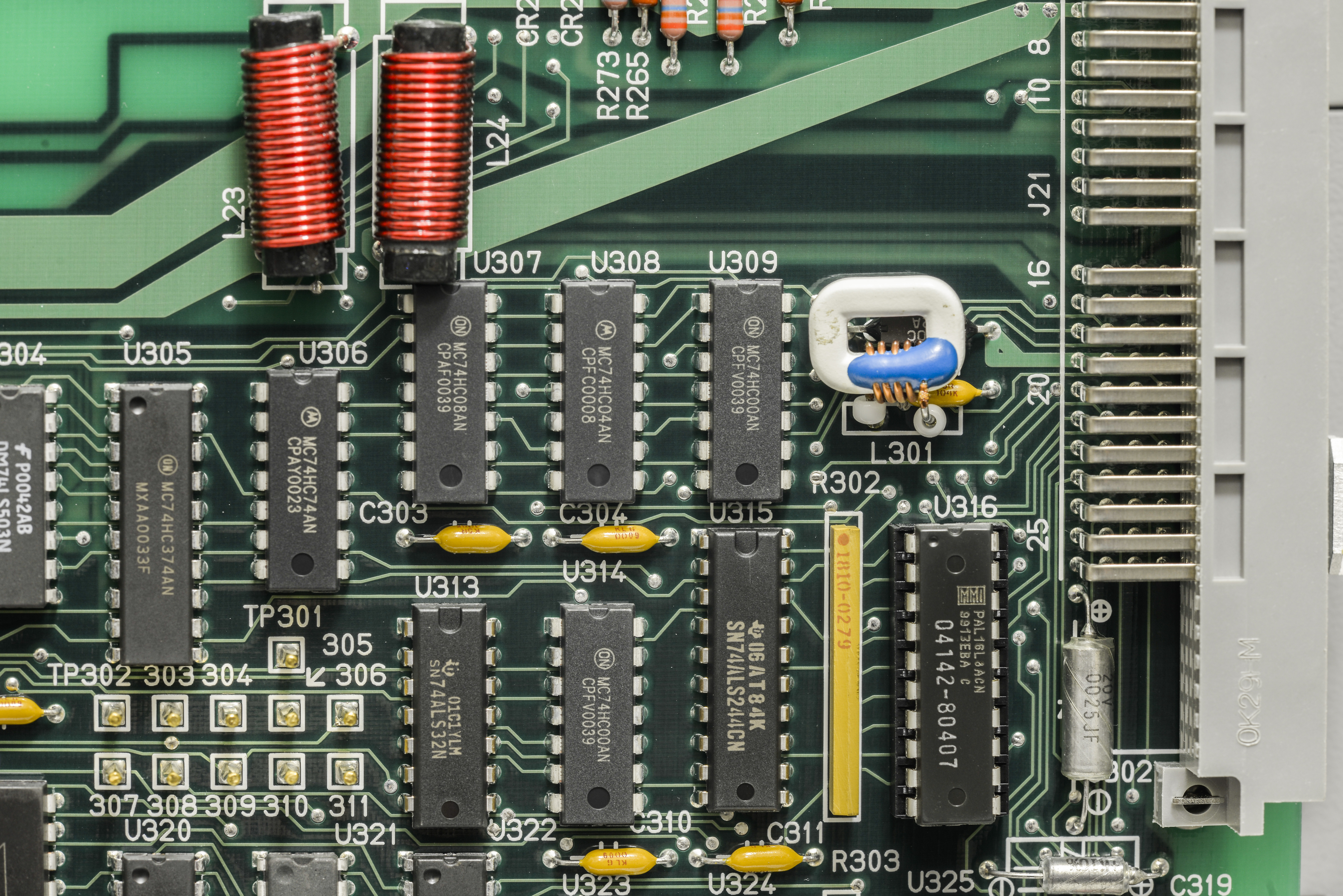
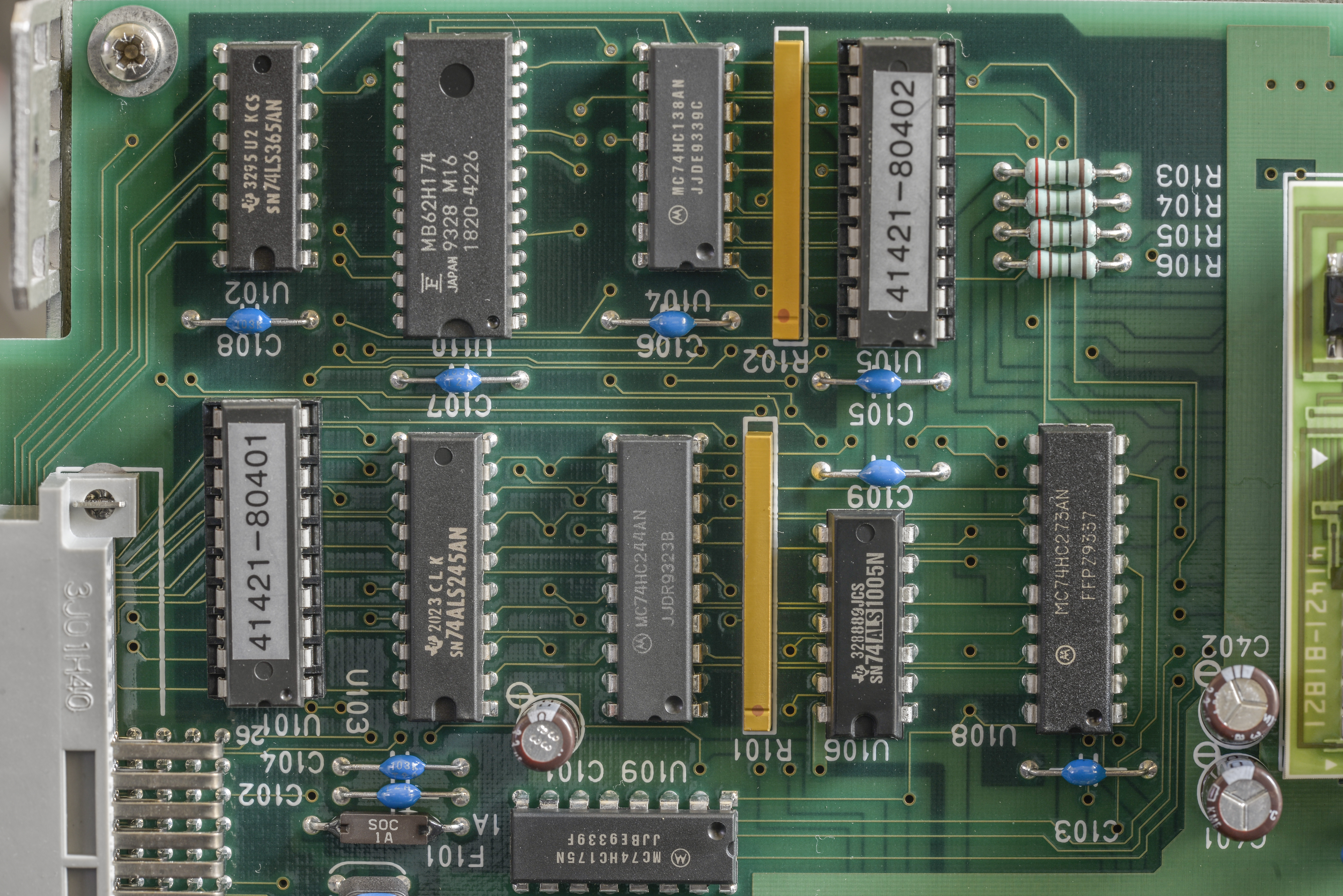
Digital board module
This board is essential for 4142B, since it contains processor, firmware and all digital logic related to mainframe operation.
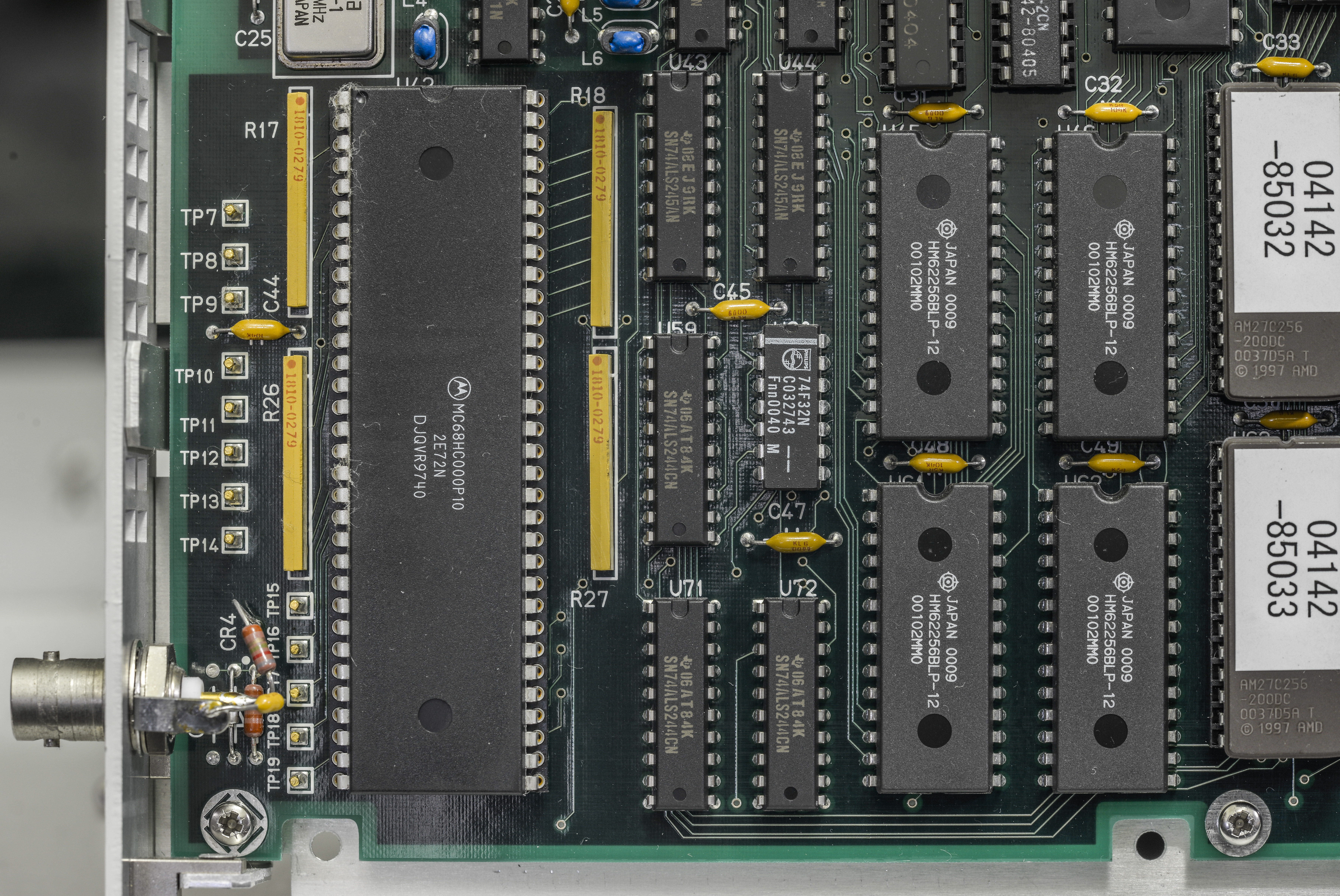
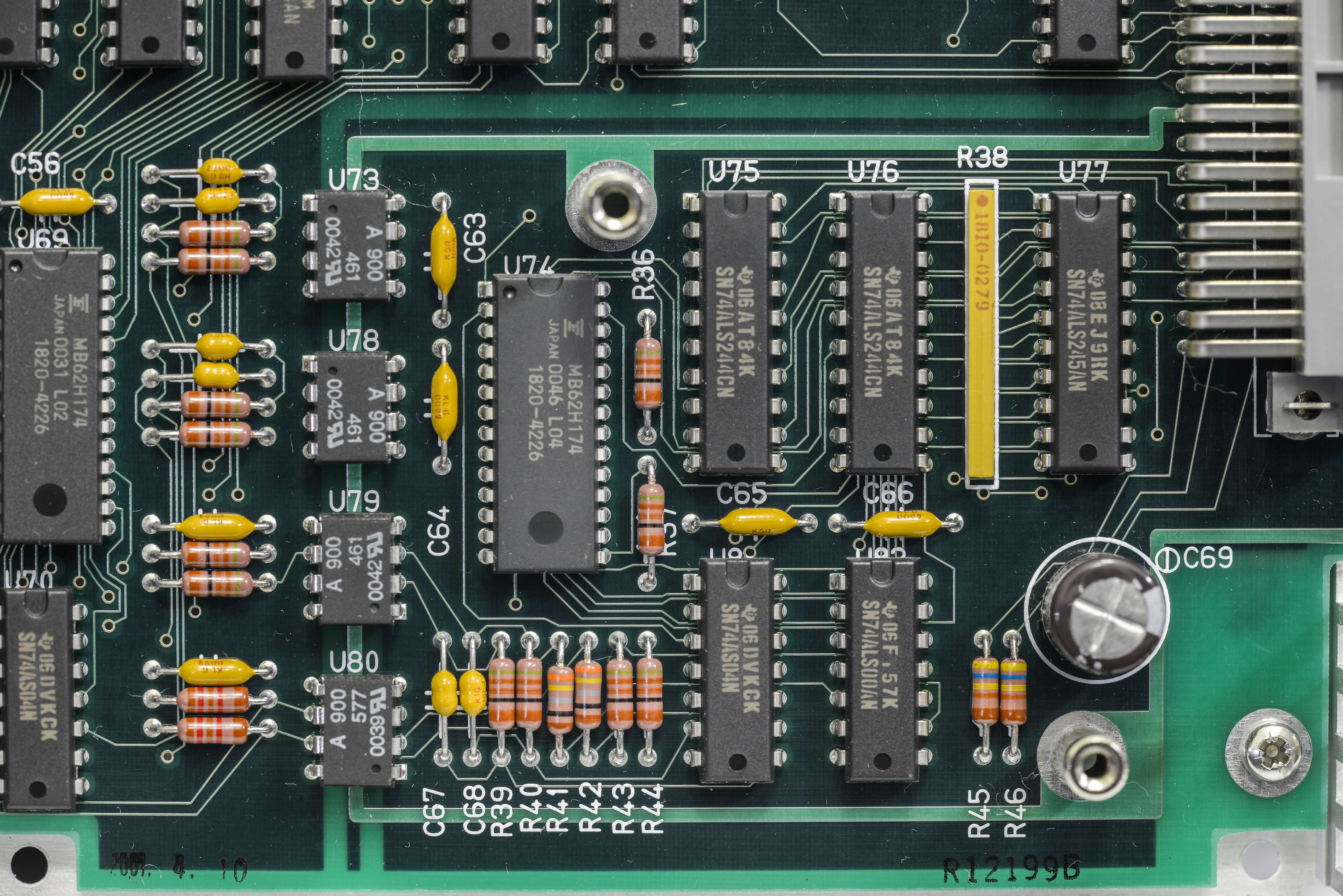
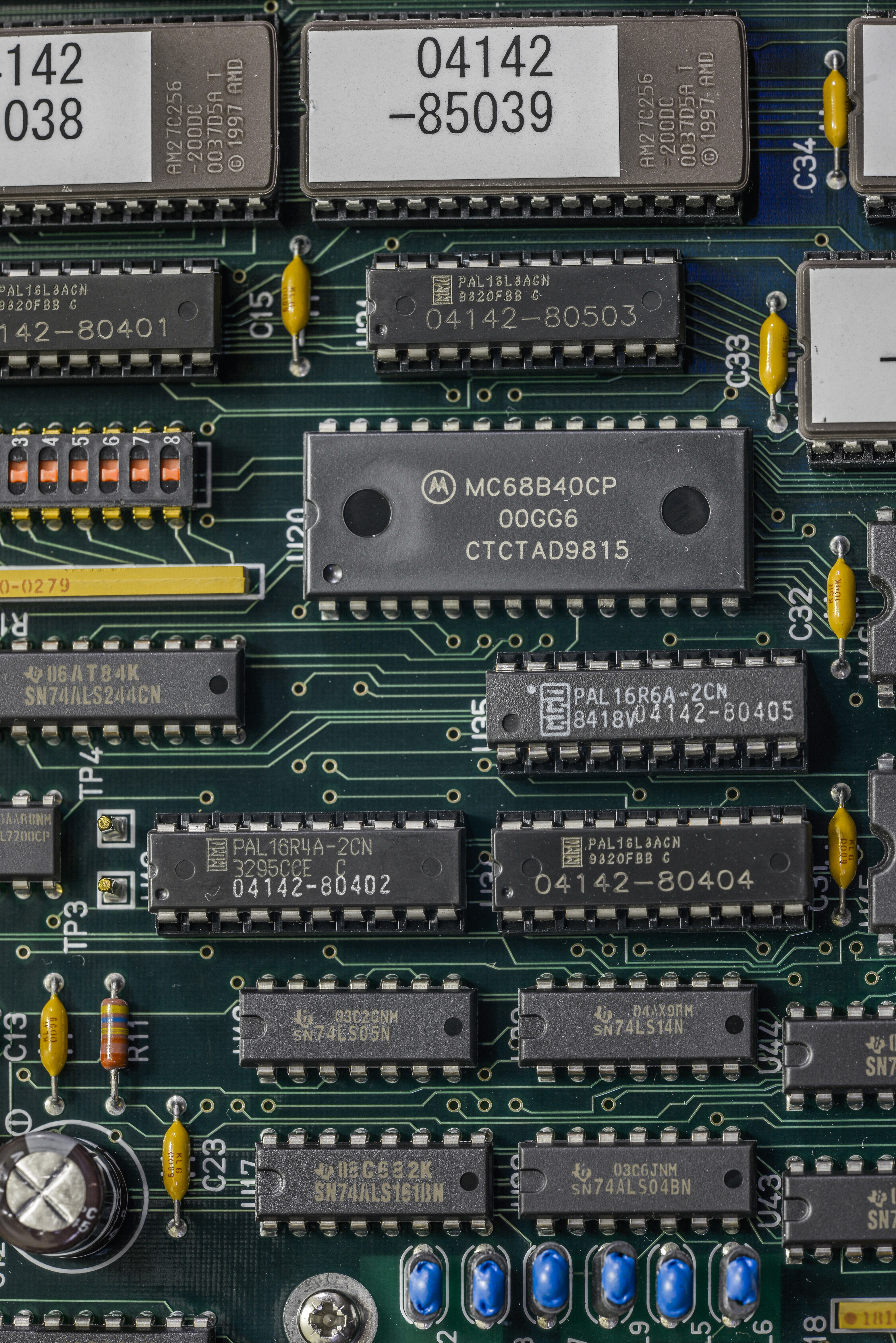
Well known Motorola 68HC000P10 is used here, just like many other instruments designed in 90’s – early 00’s. There are four package of 120ns SRAM nearby, made by Hitachi HM62256BLP-12.
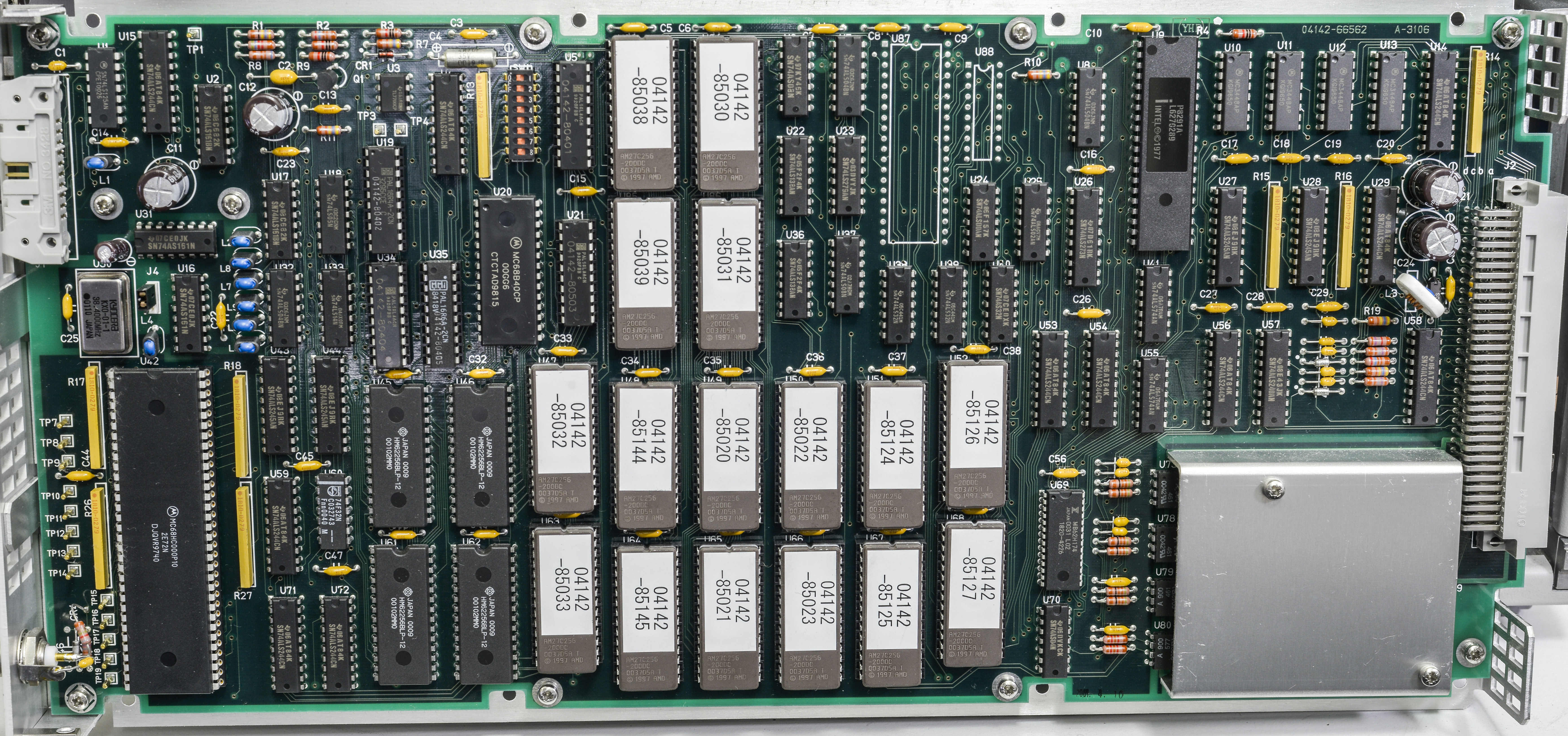
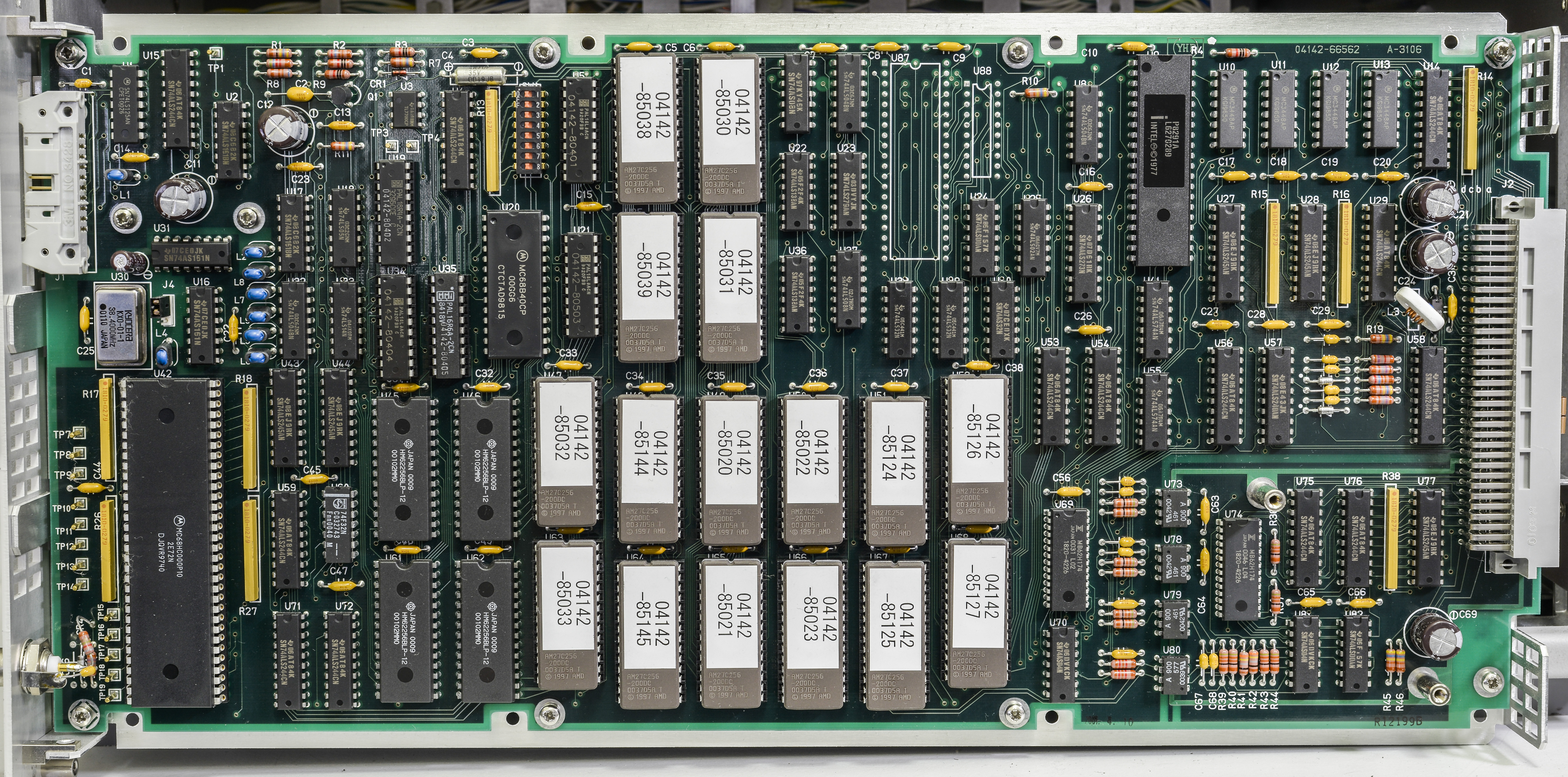
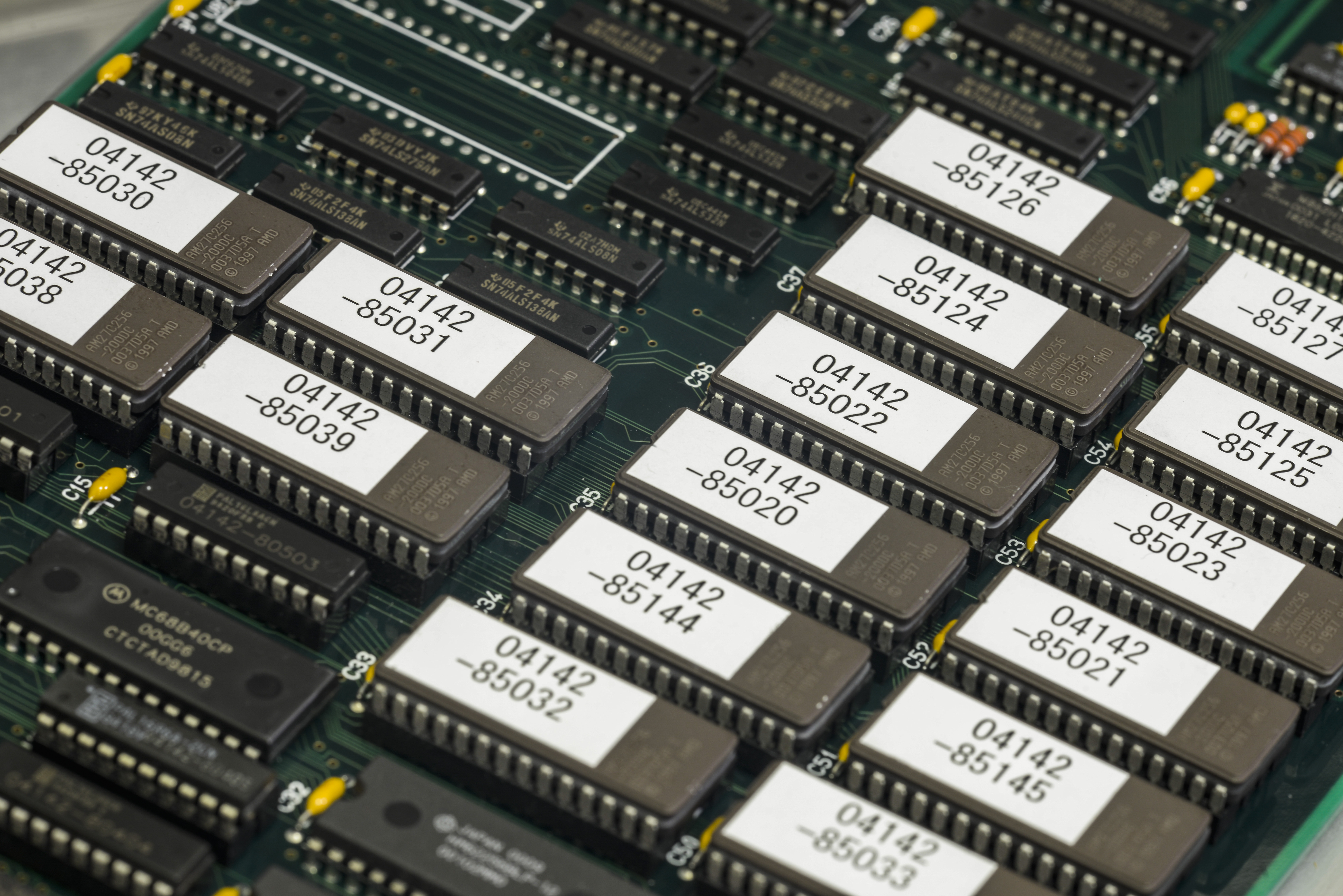
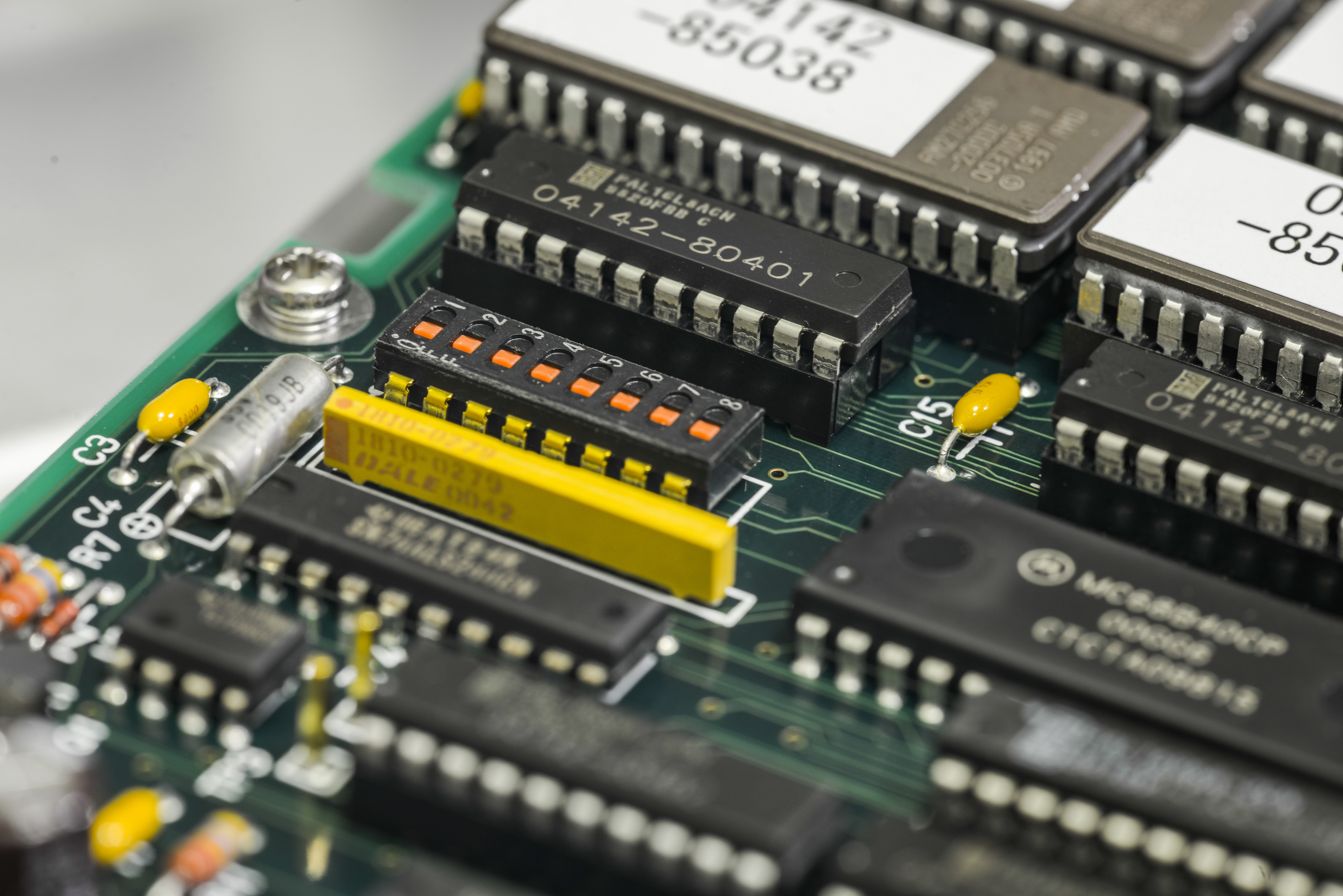
I never saw instrument with 16 pieces UV EPROMs to store firmware. All of them were read using TL866CS and presented in firmware section of this article.
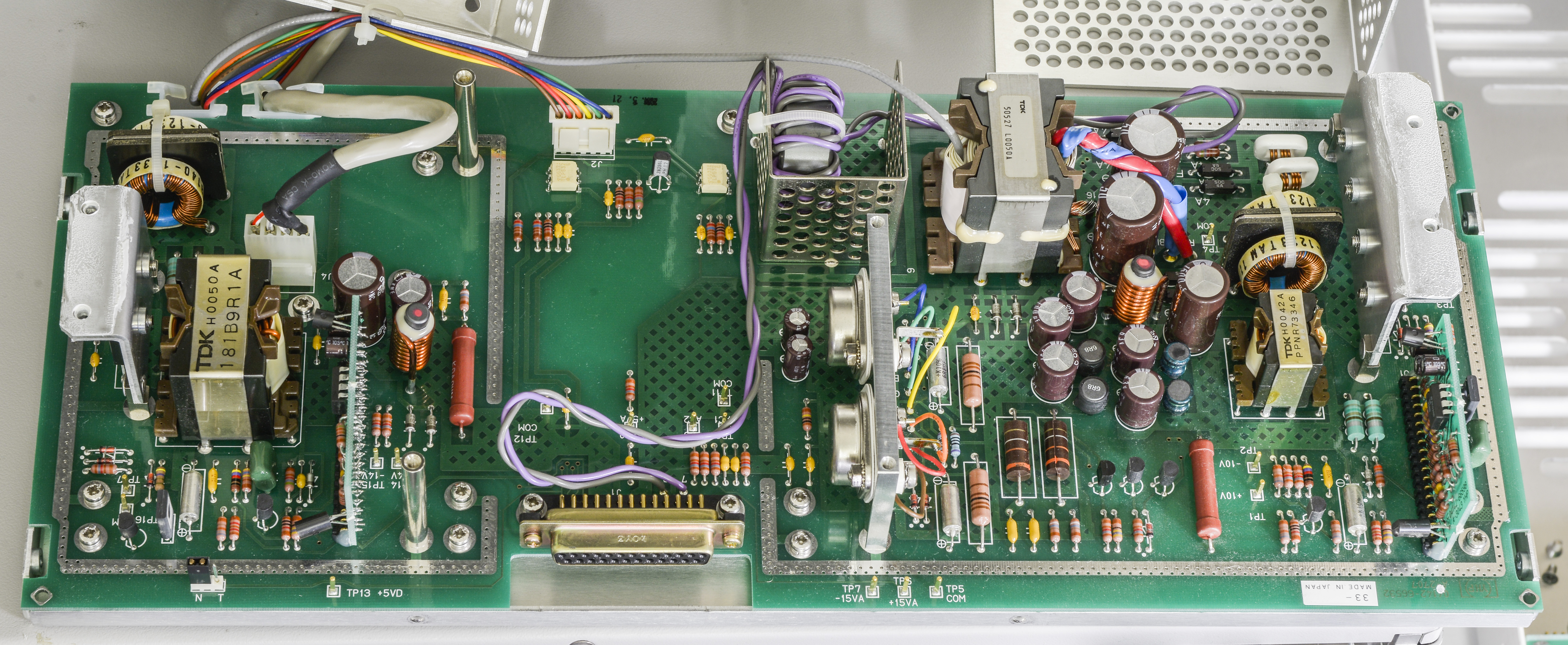
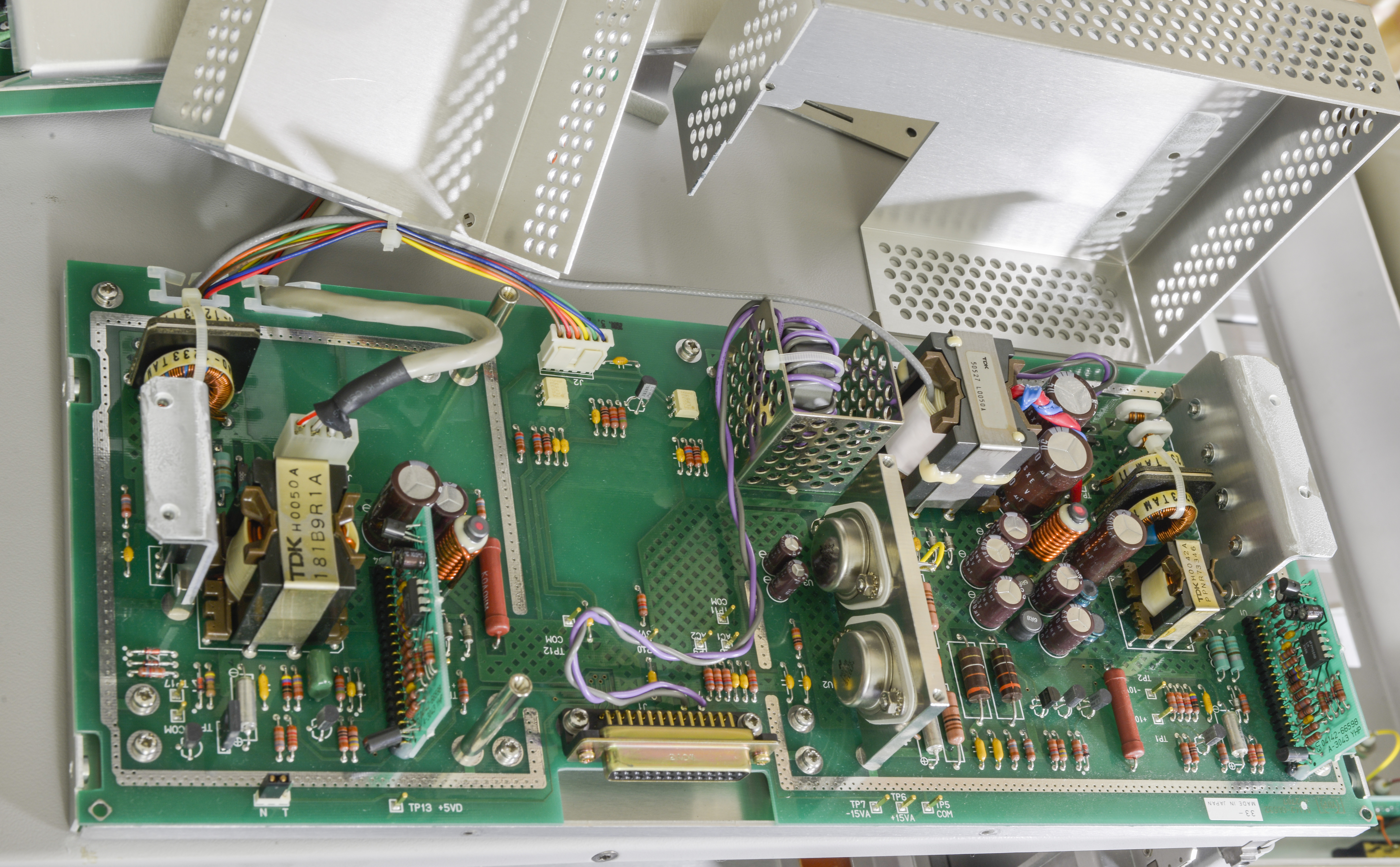
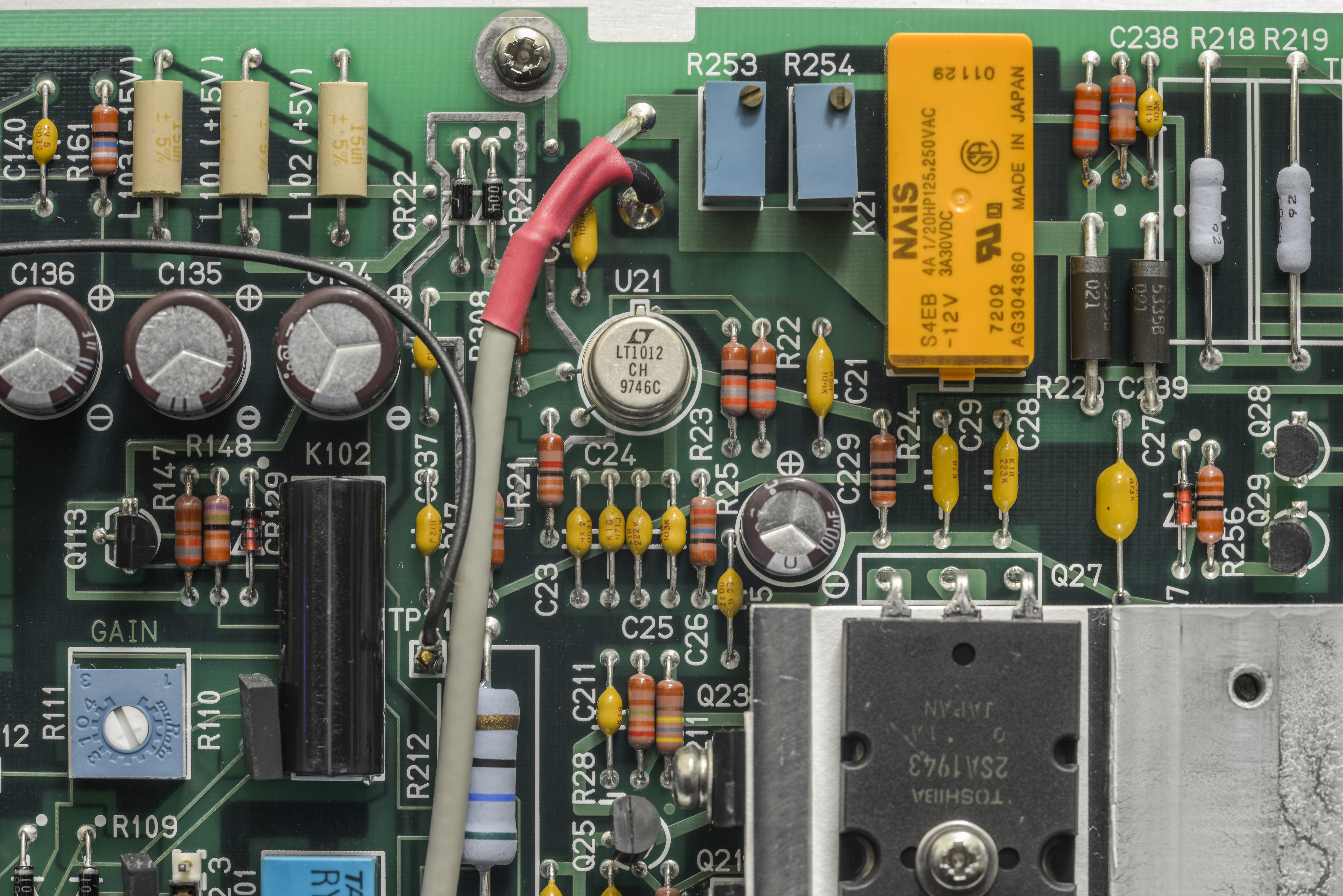
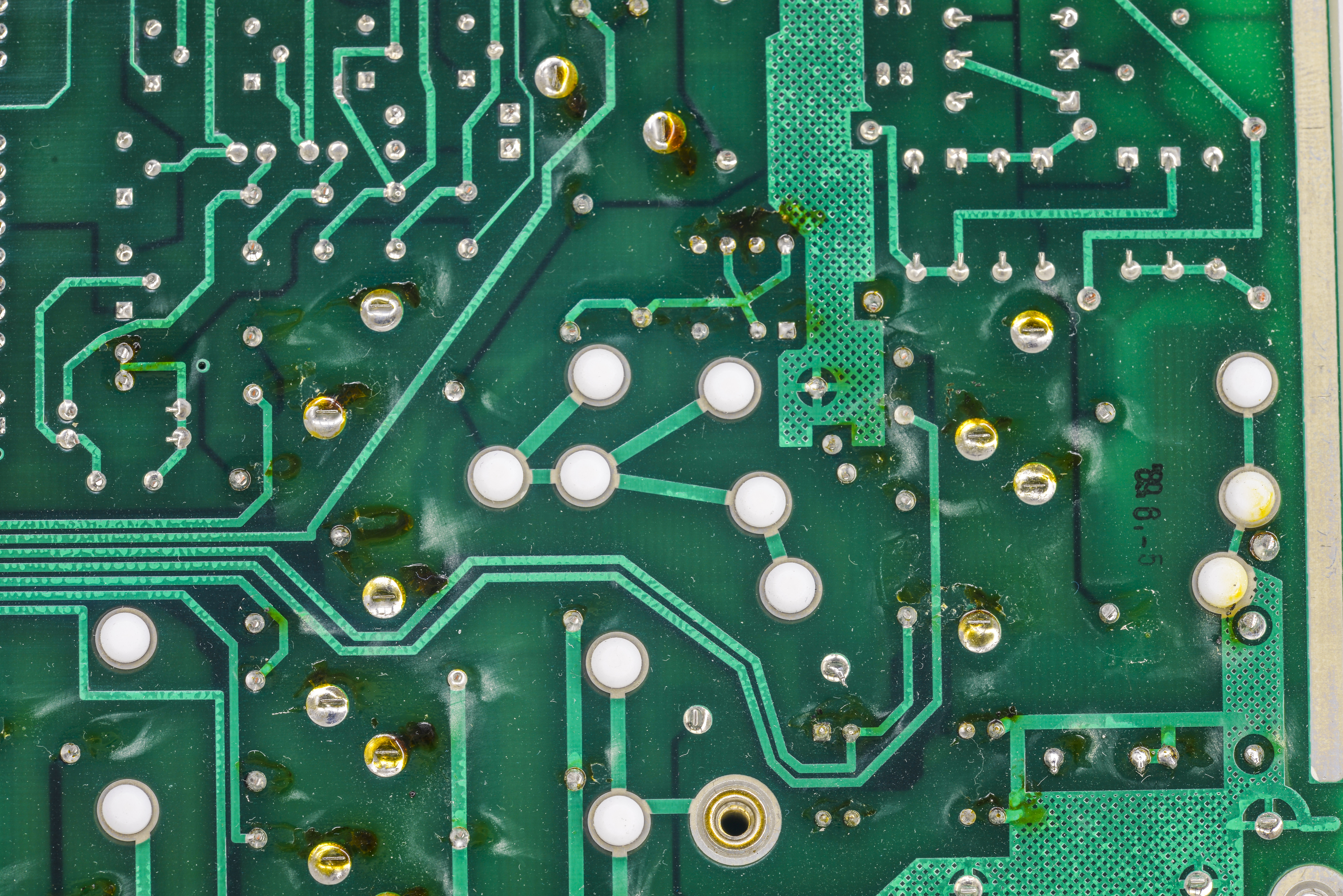
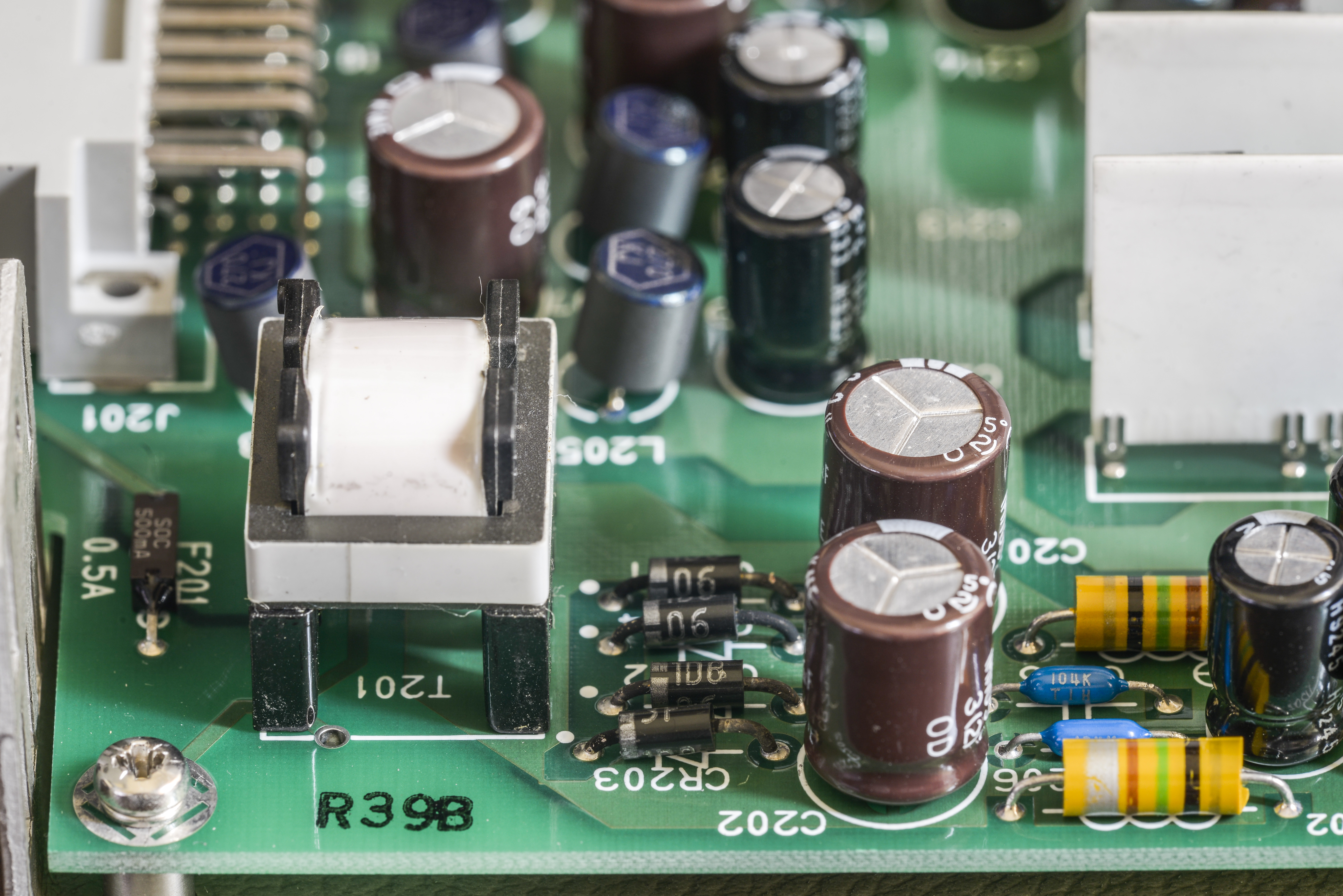
Power supply assembly
There are very high-quality RIFA film capacitors and common-mode filters.
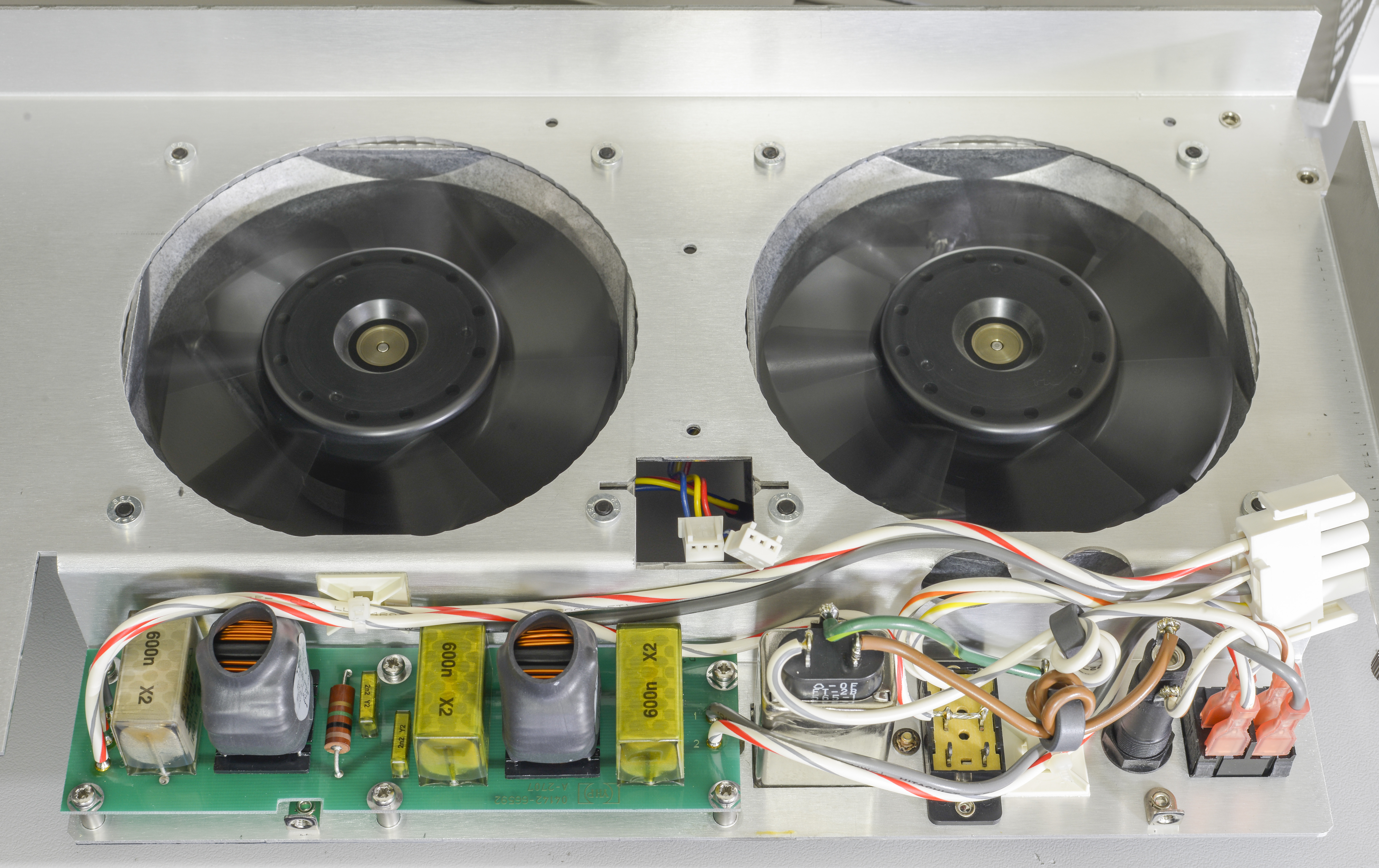
Filtered mains plugged directly into PSU via robust 4-pin connector. FANs connected by pair of three-wire connectors, likely for tachometer monitoring.
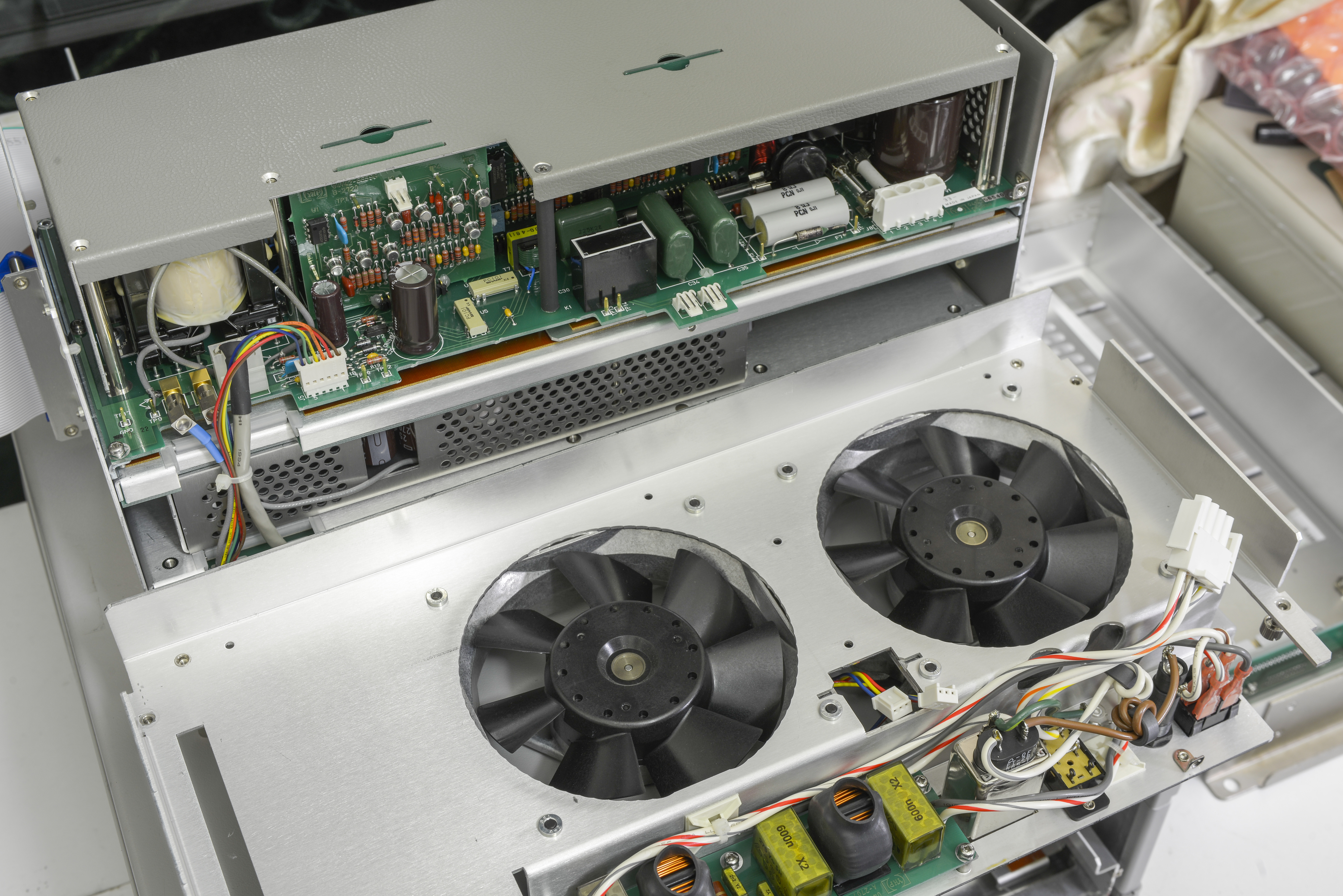
Capacitors are no usual cheapies, but triple 4-wire ones, which have actually three capacitor cells inside, rated at 820µF x 250V, manufactured by Nippon Chemi-Con KMG series.
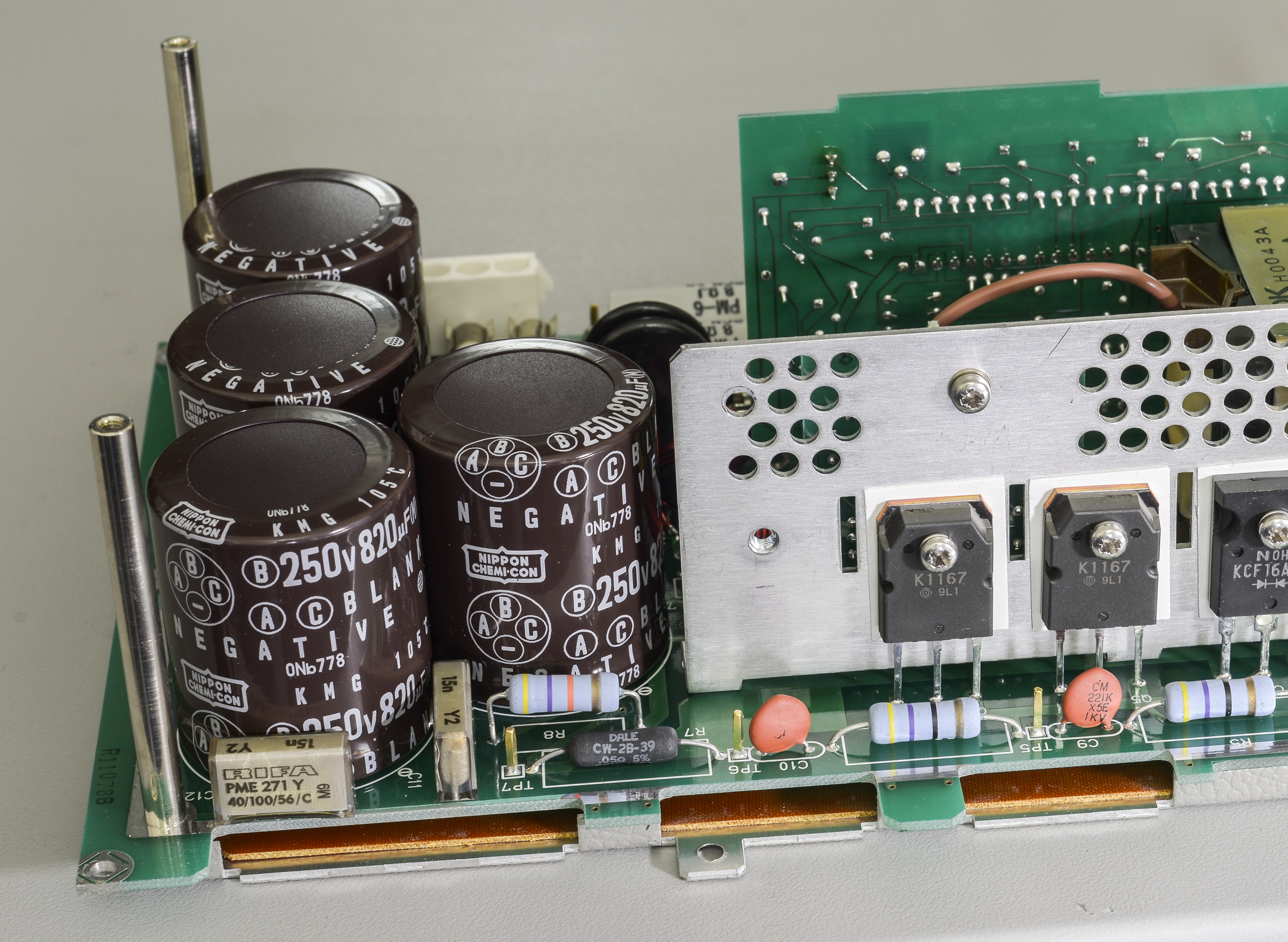
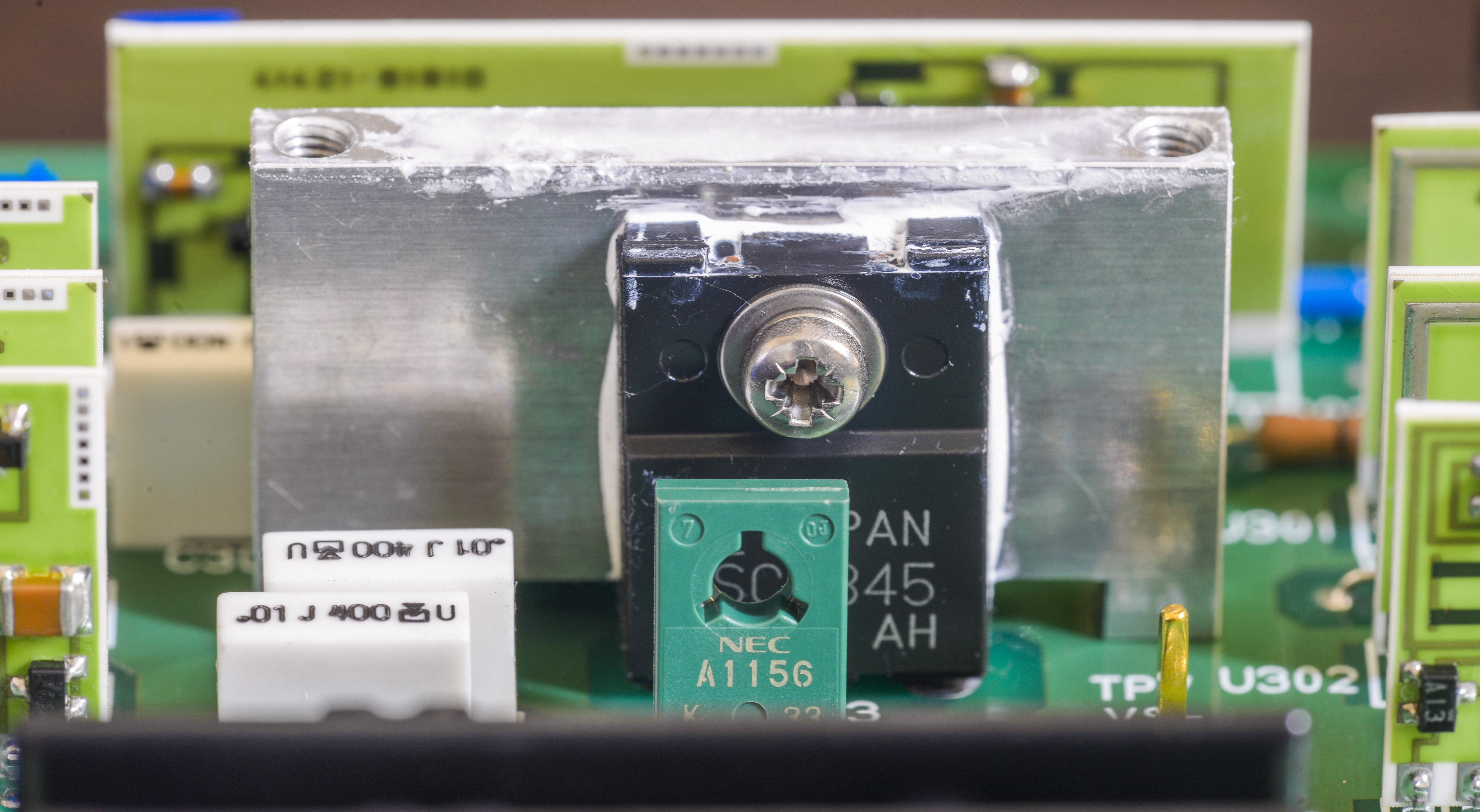
Array of TO-247 transistors mounted on aluminum plate to provided enough cooling under heavy load conditions.
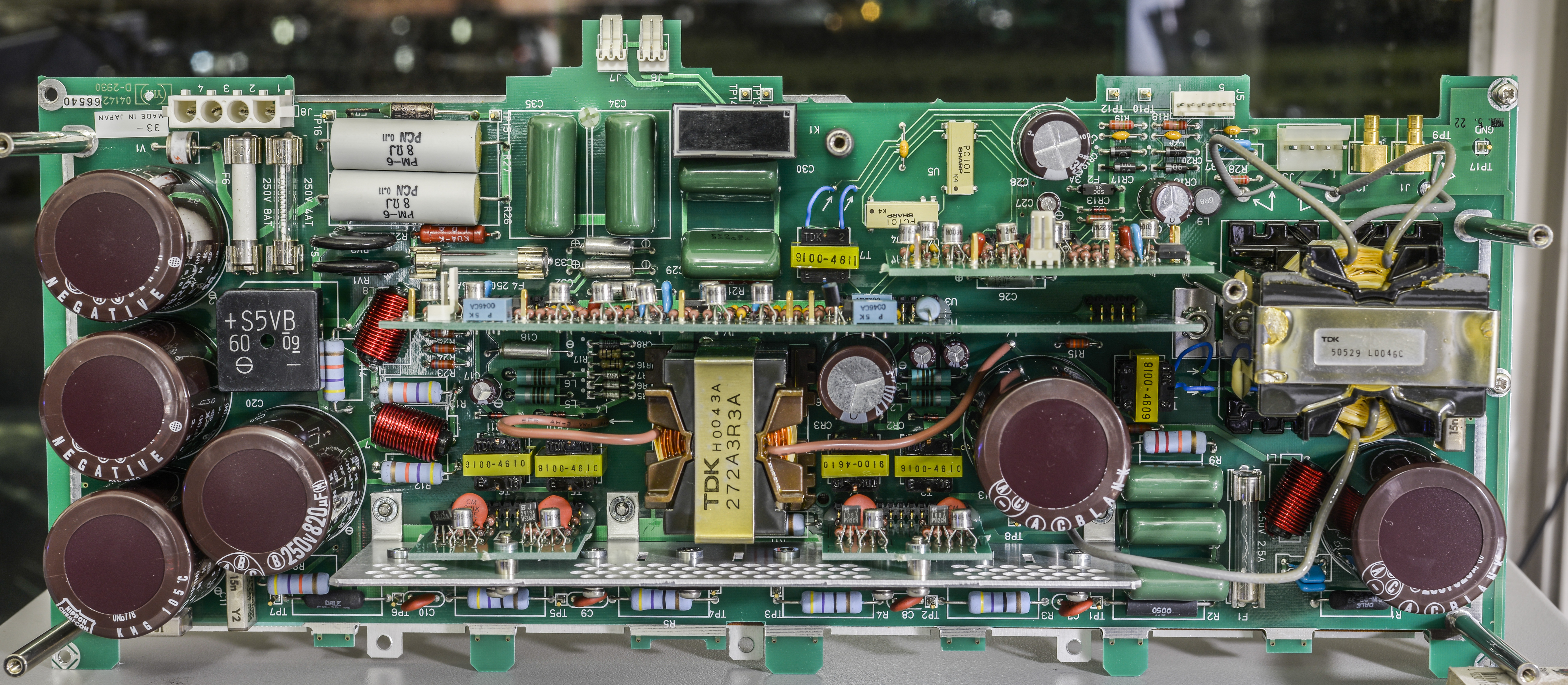
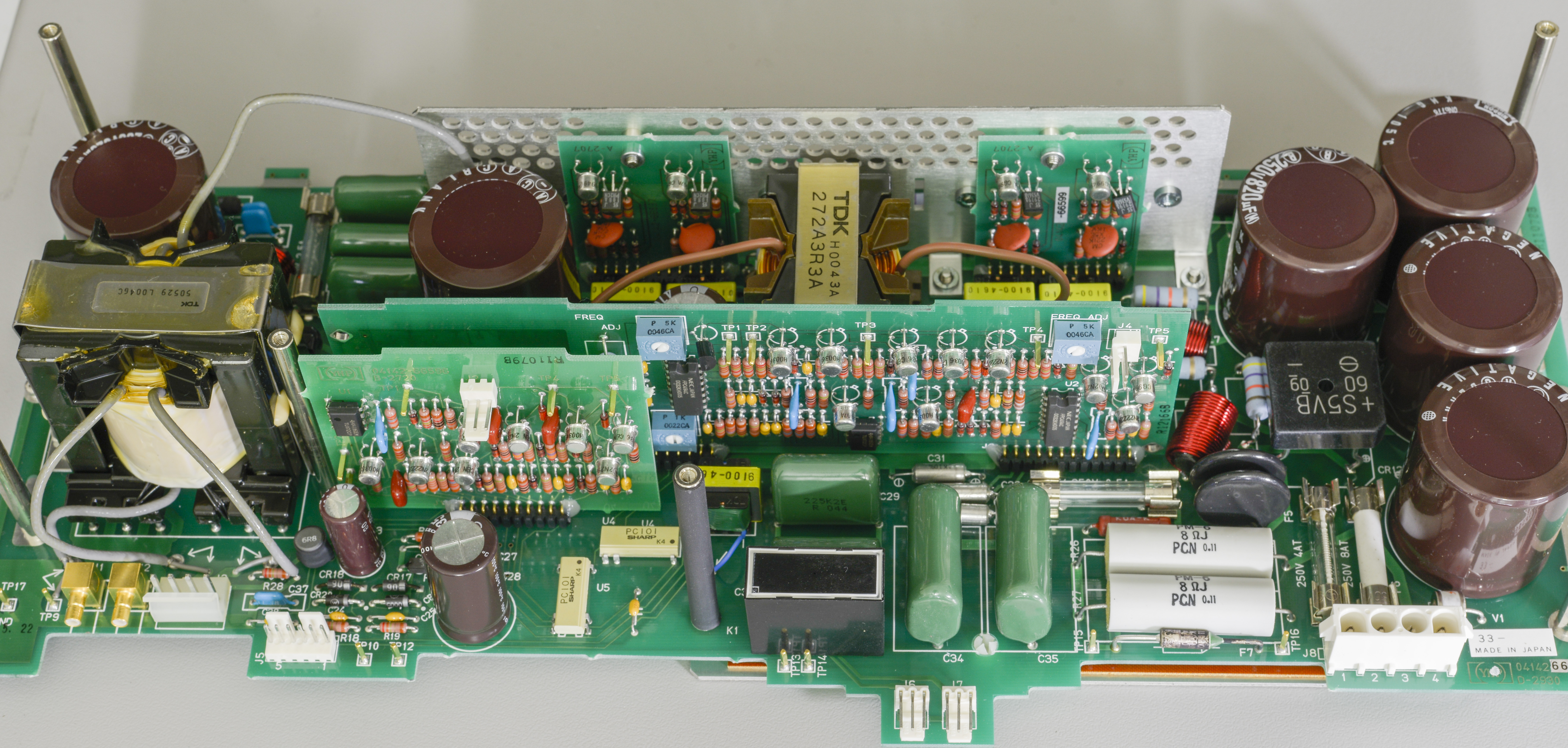
This power supply is rather unusual dual-conversion topology to reduce coupling and noise pickup from mains. Center TDK coil is a filter on E-type core, while larger transformer on the right corner is actual main core transformer, with both regular windings and coaxial wire windings.


Let’s a look on block diagram schematics from the service manual.
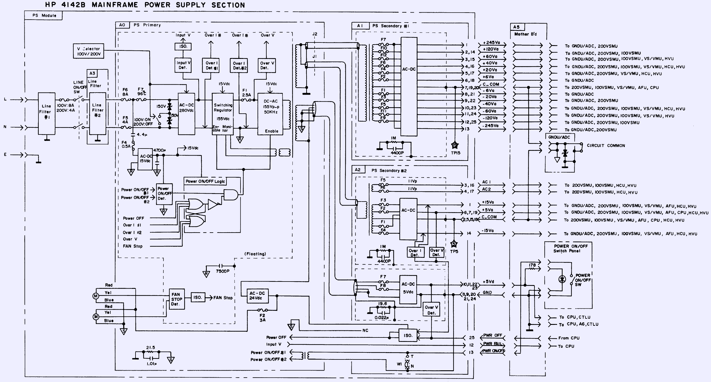
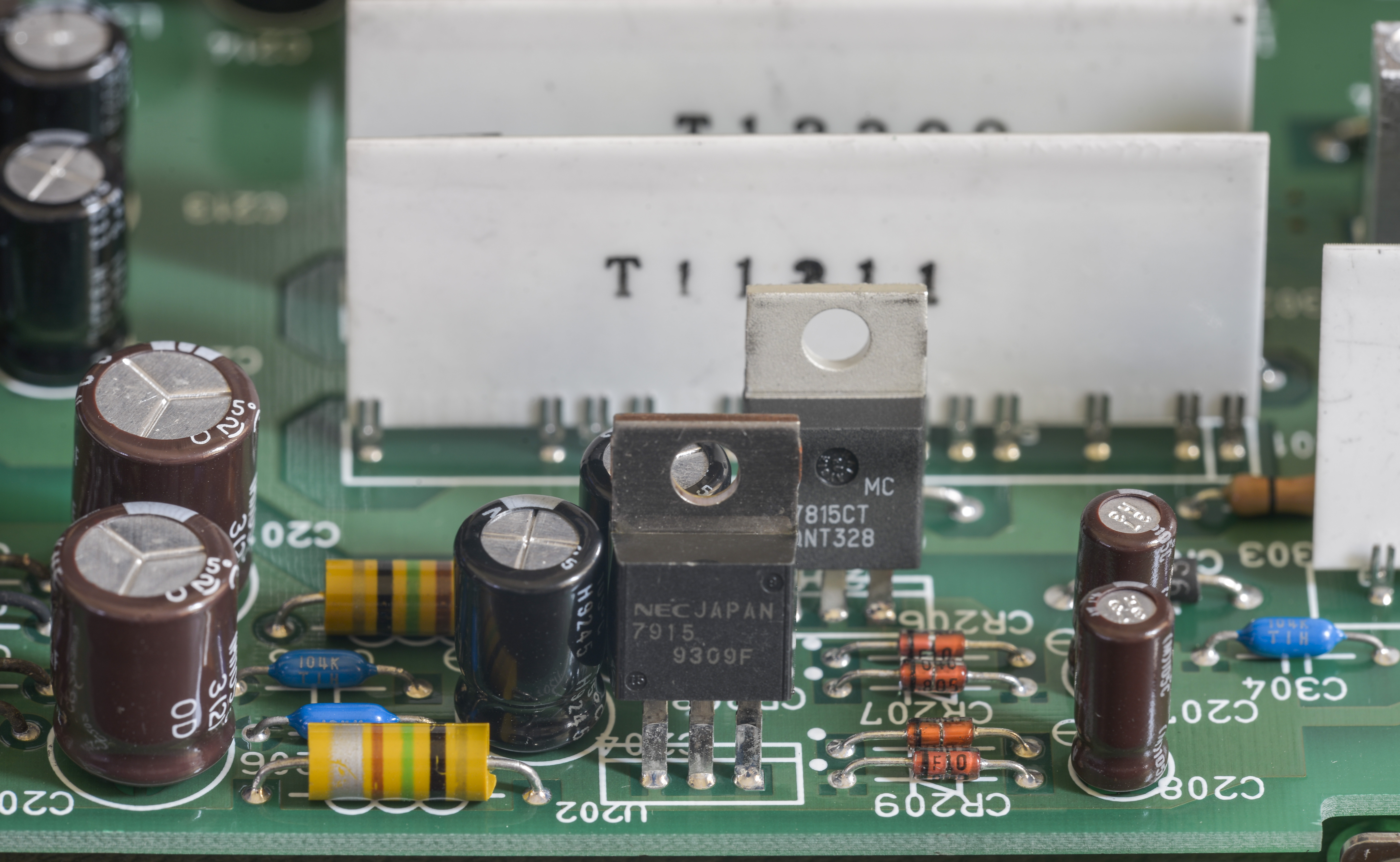
PSU converts mains into +155VDC high power rail, which further converted by second DC-AC to 155Vpk-pk at 50kHz. Output of this converter is supplied to secondary power supply, located on another board to further AC-DC stage to provide all needed voltages for analog and digital modules.

Secondary PSUs use own transformers and protection circuits, as well as own filtering and rectification.
All domains and supply sections are individually shielded by grounded aluminum cages to avoid EMI radiation into the mainframe.
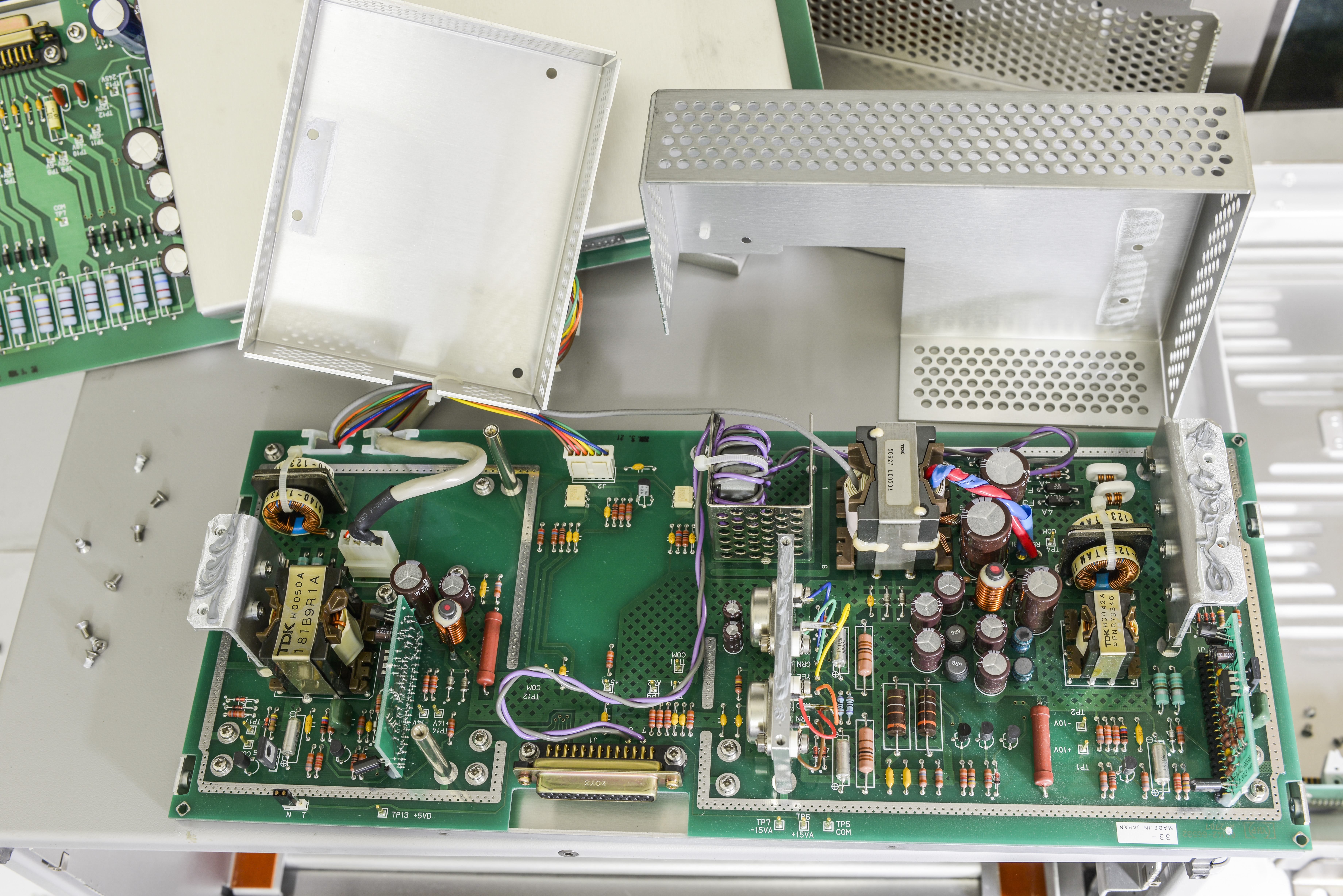
Parts are held together in one piece by various panels and chassis parts.

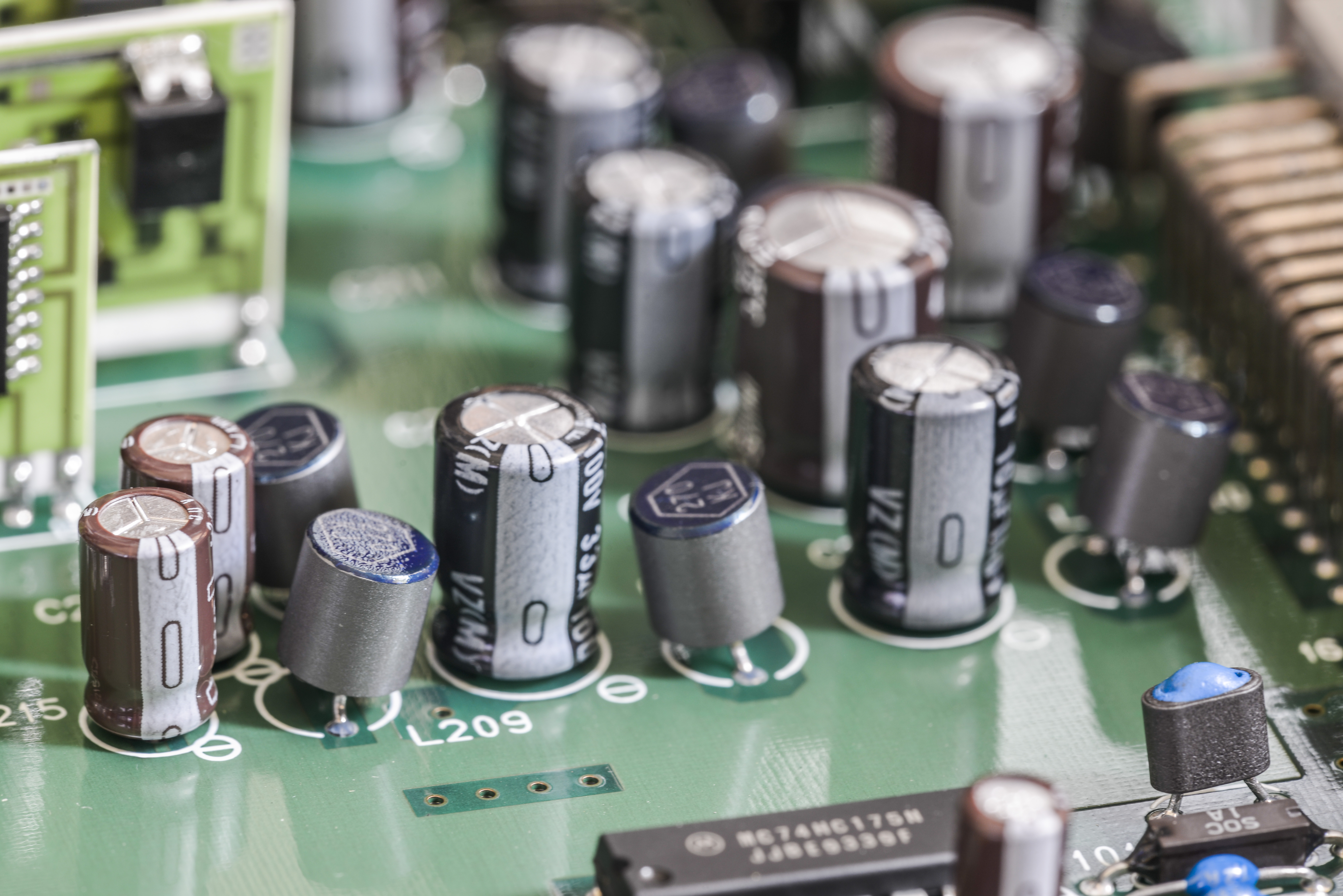
There are great lot of capacitors everywhere on power boards, all are +105°C made by Nippon Chemi-Con. No unknown brands in instrument like this, where reliability is a key of long service and constant operation.


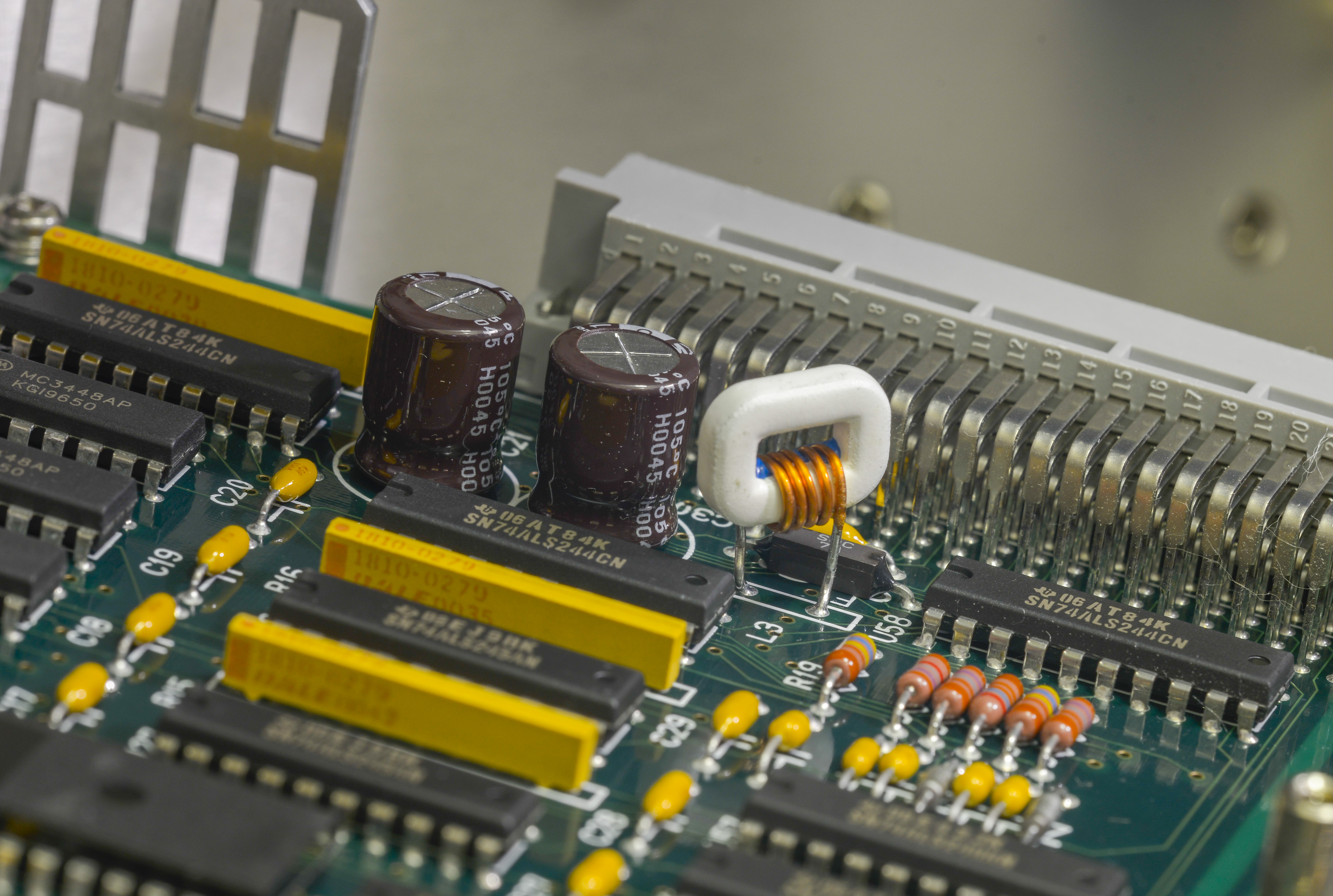
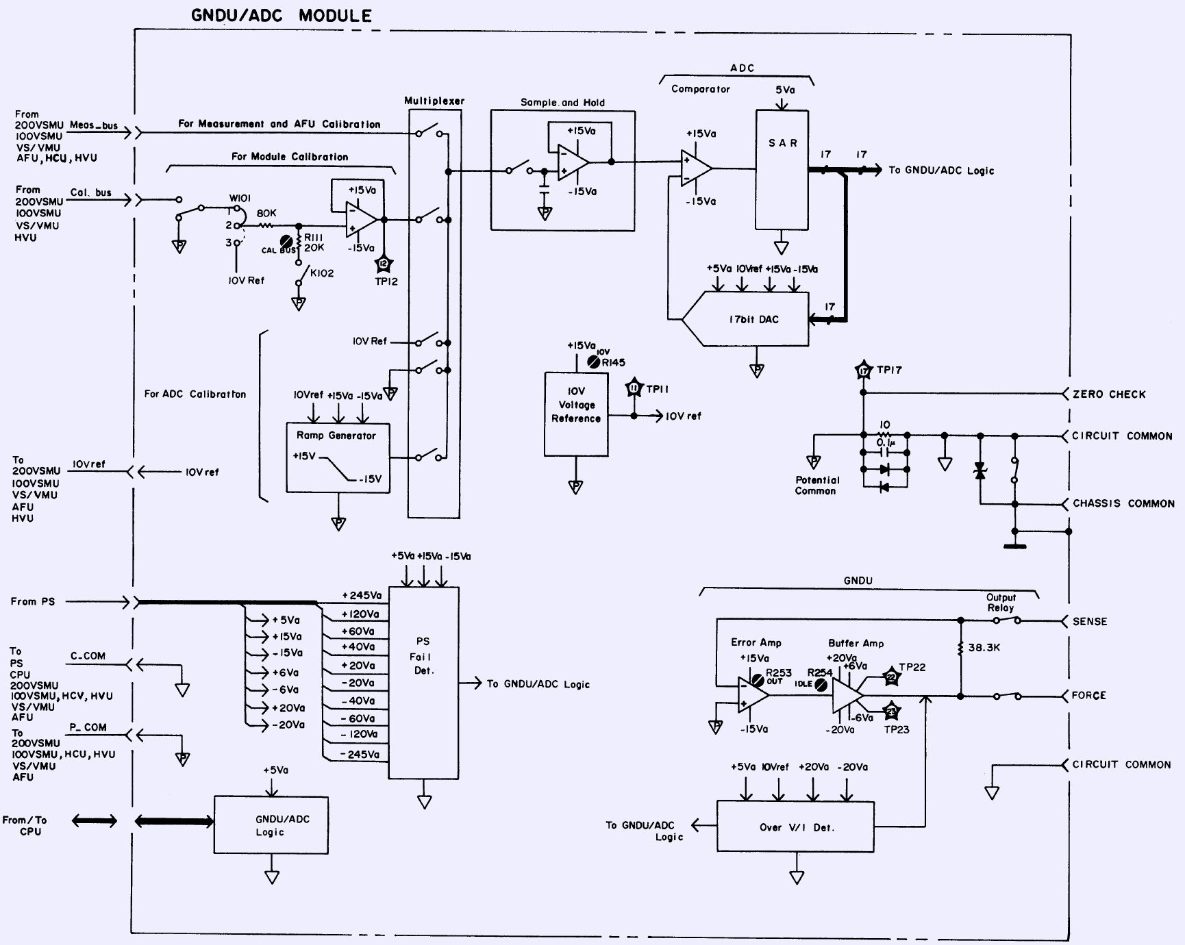
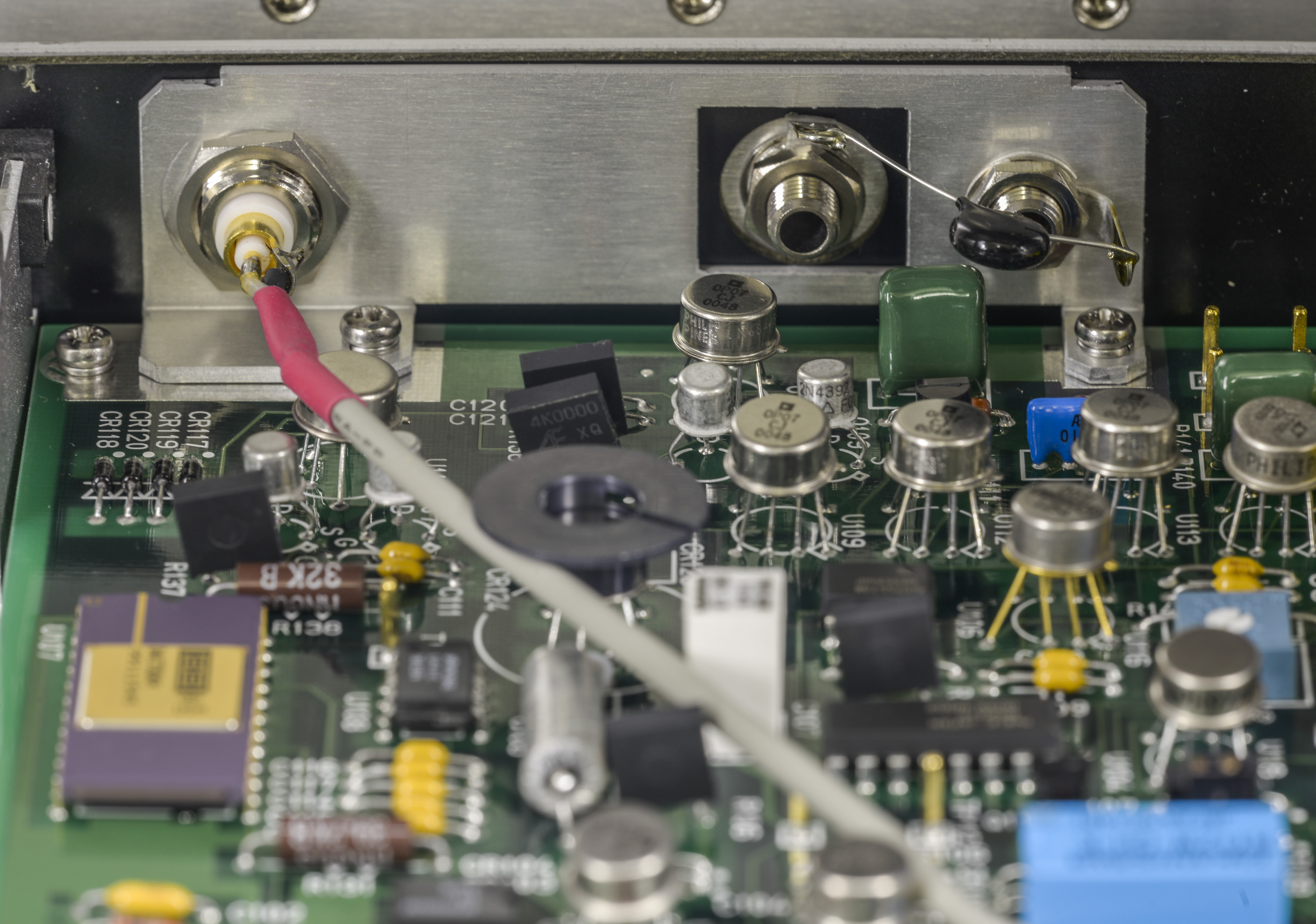
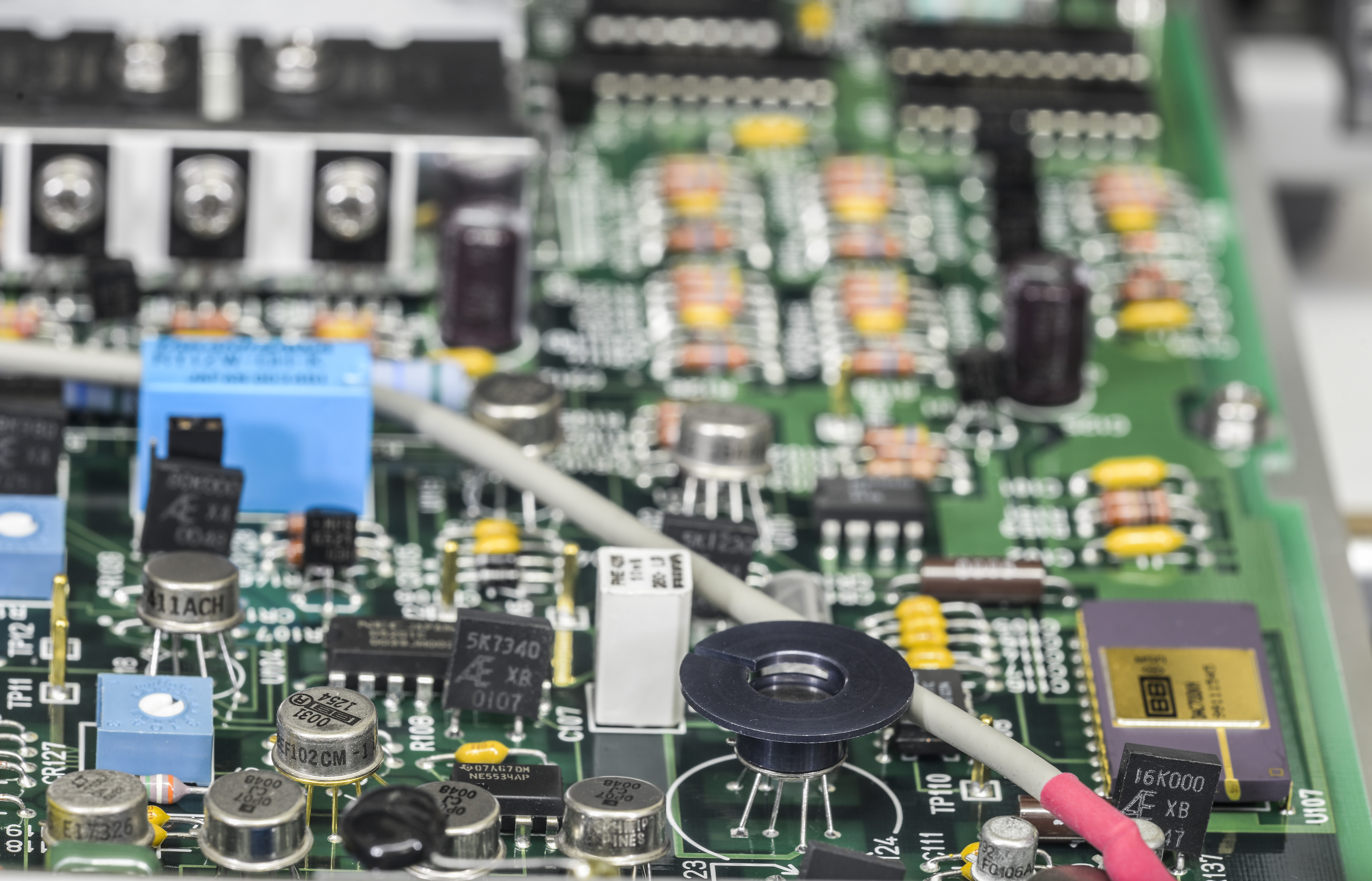
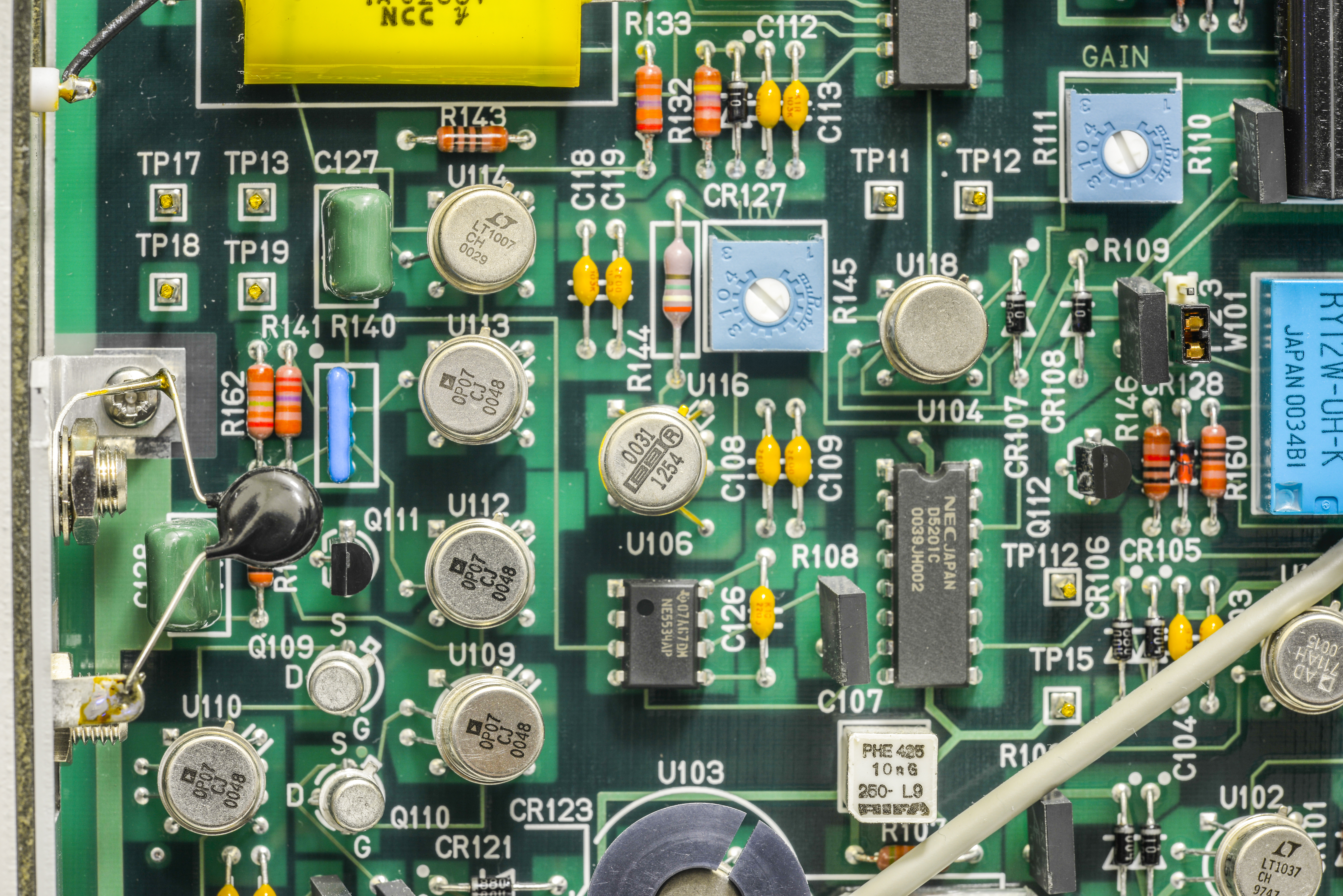
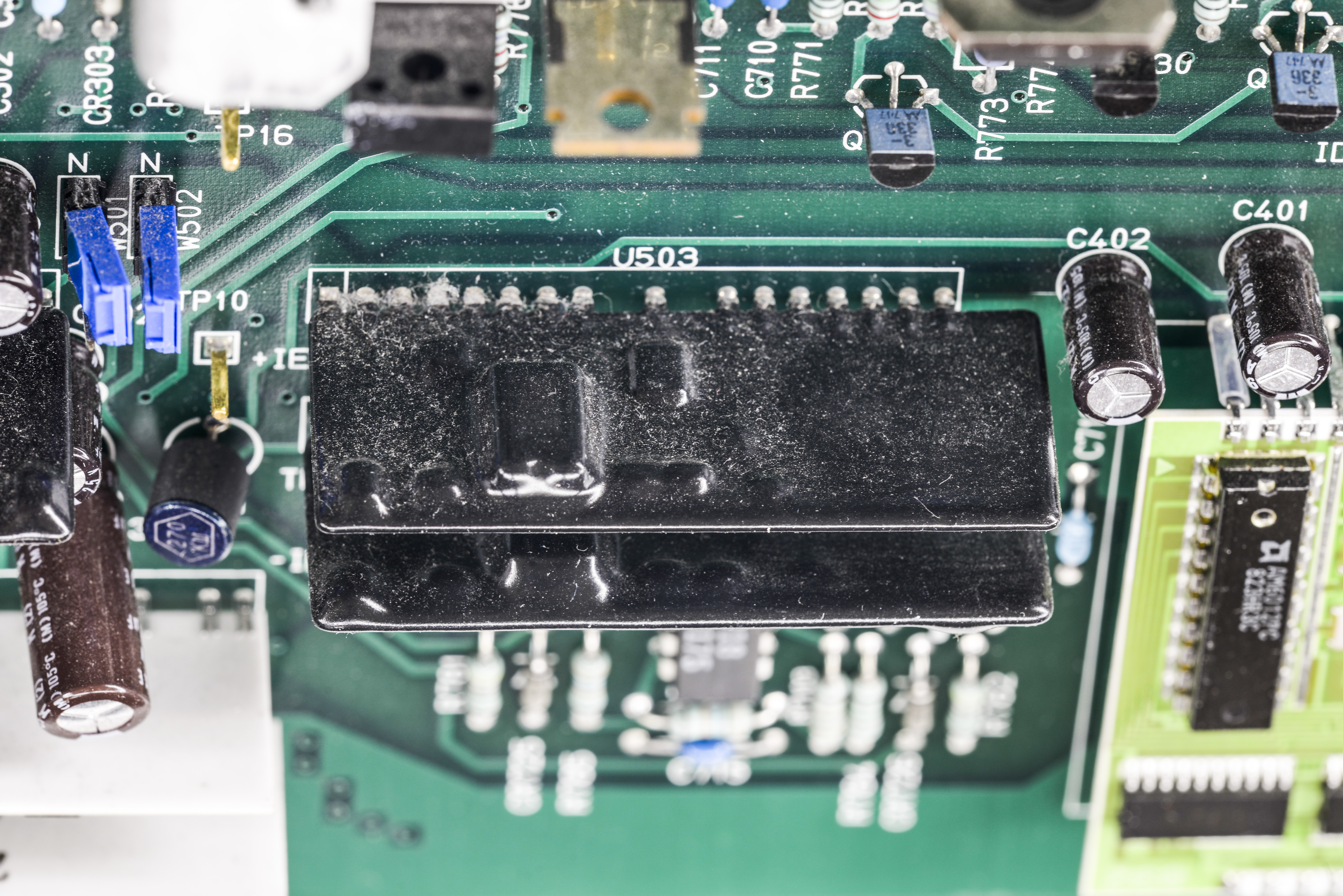
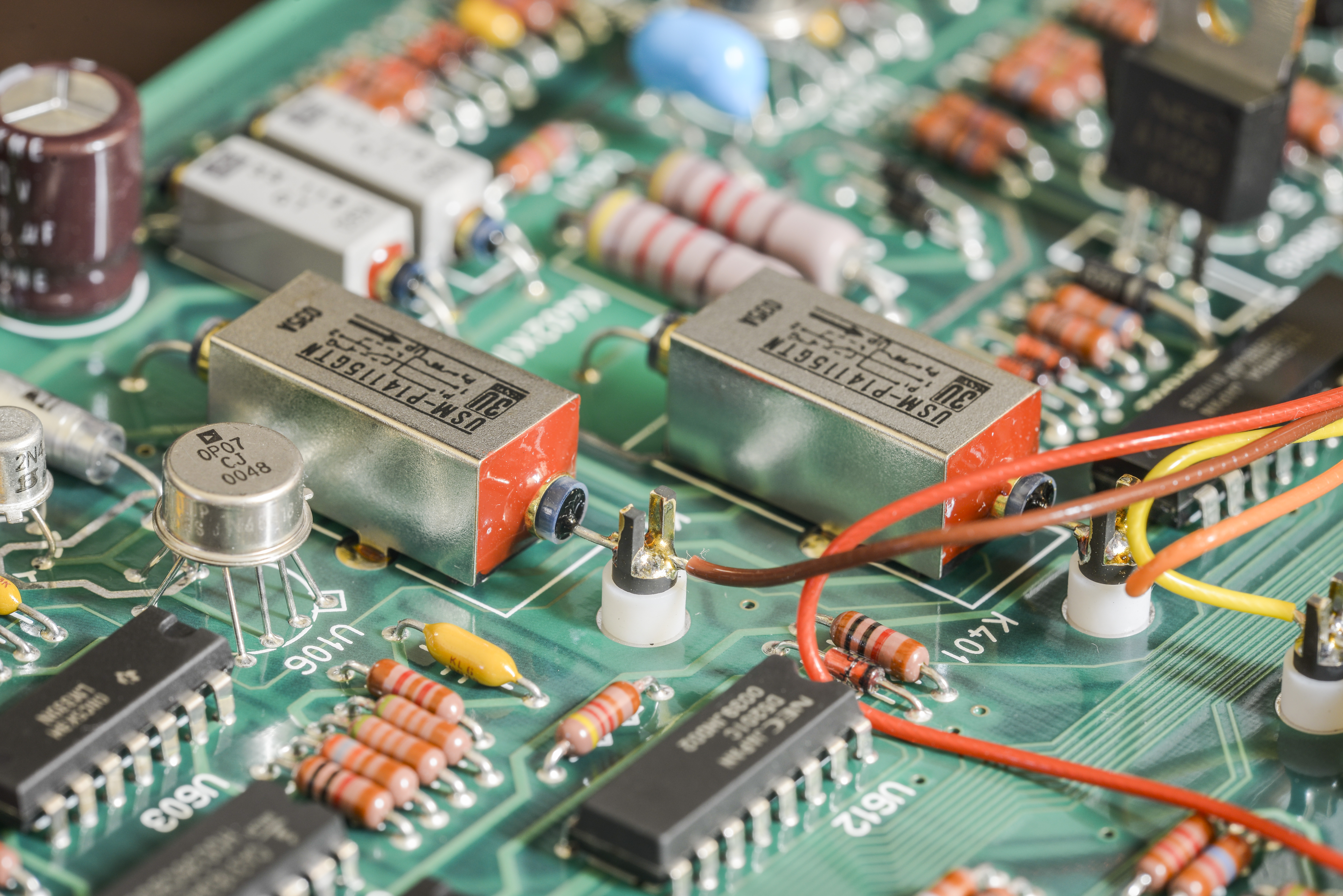
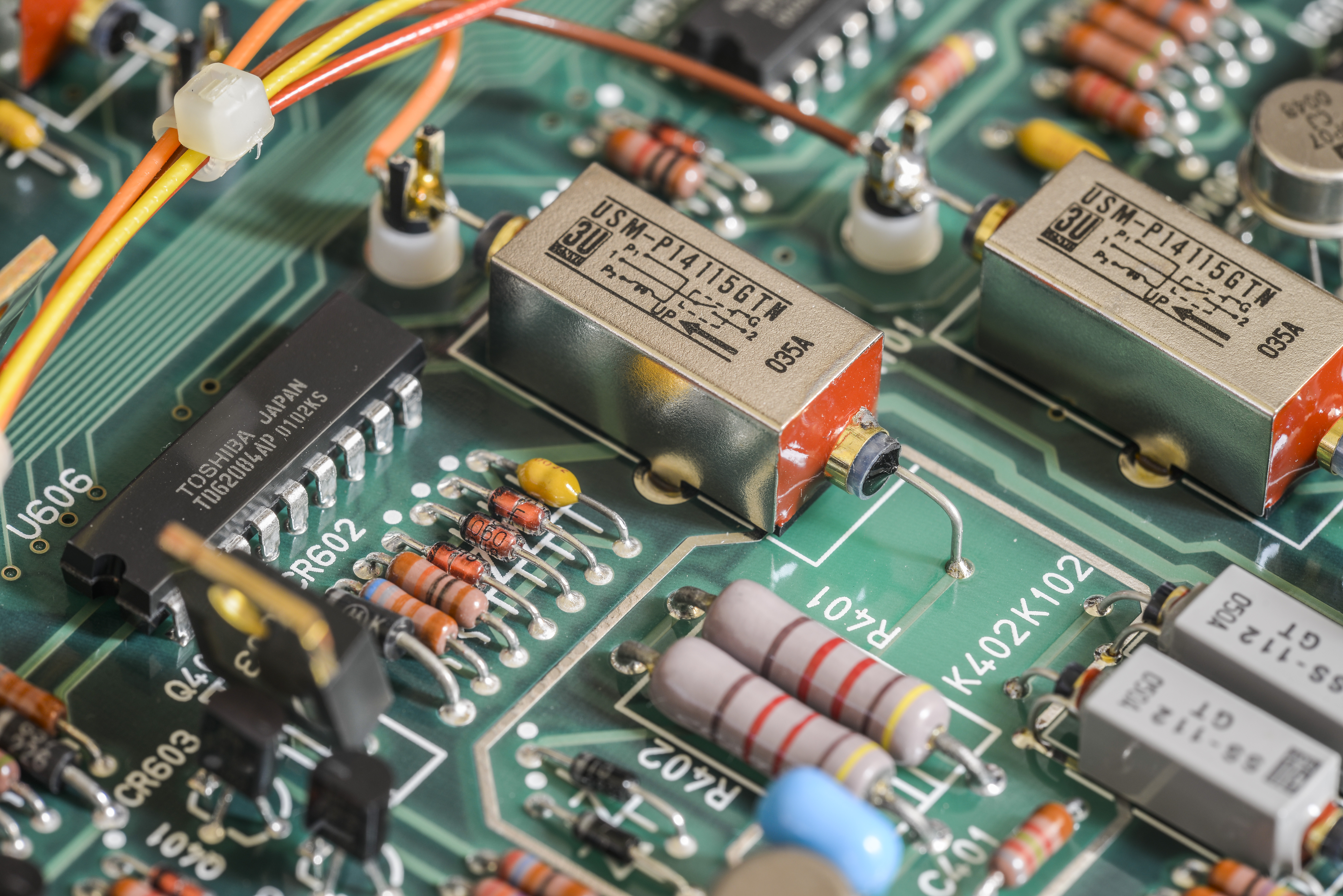
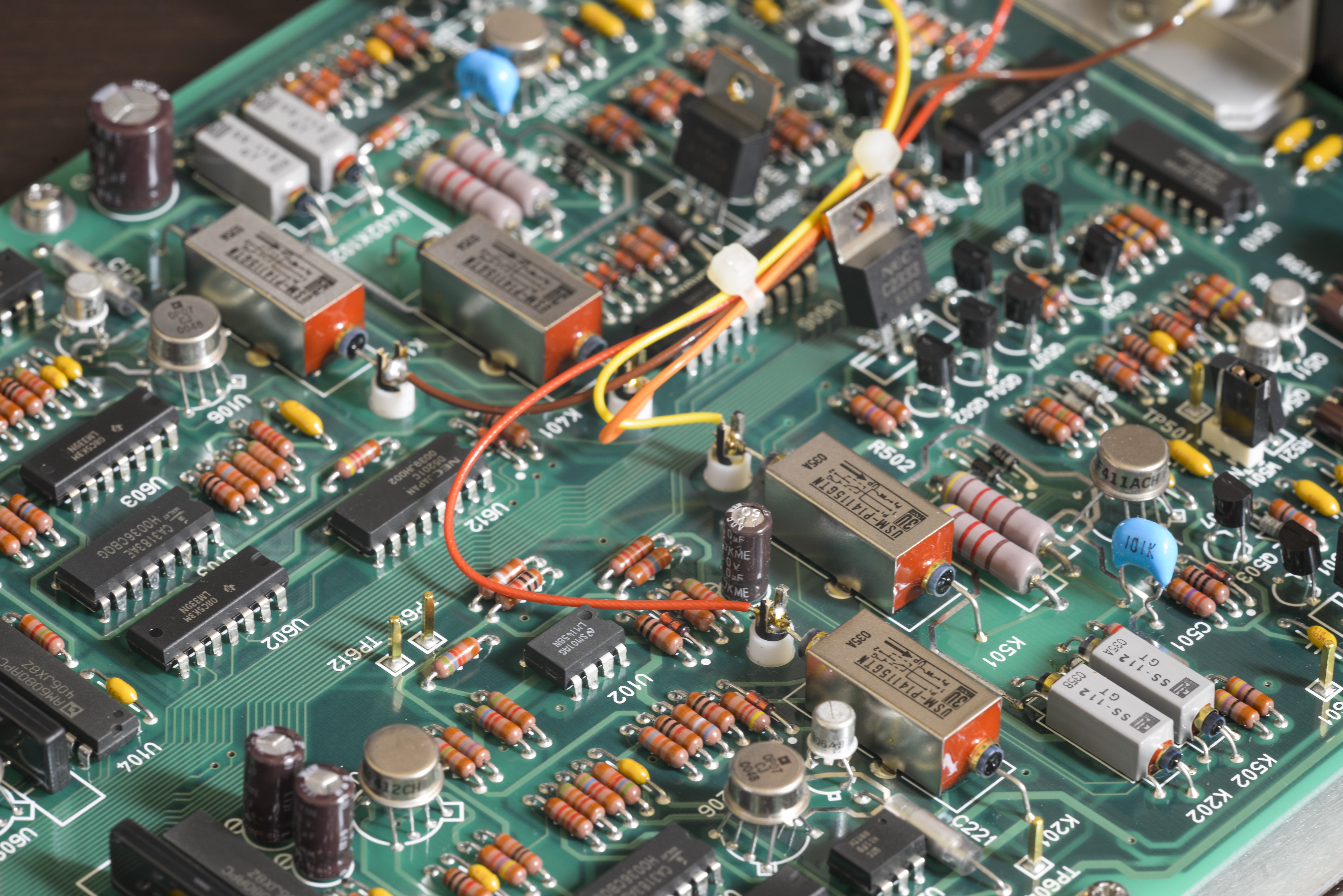
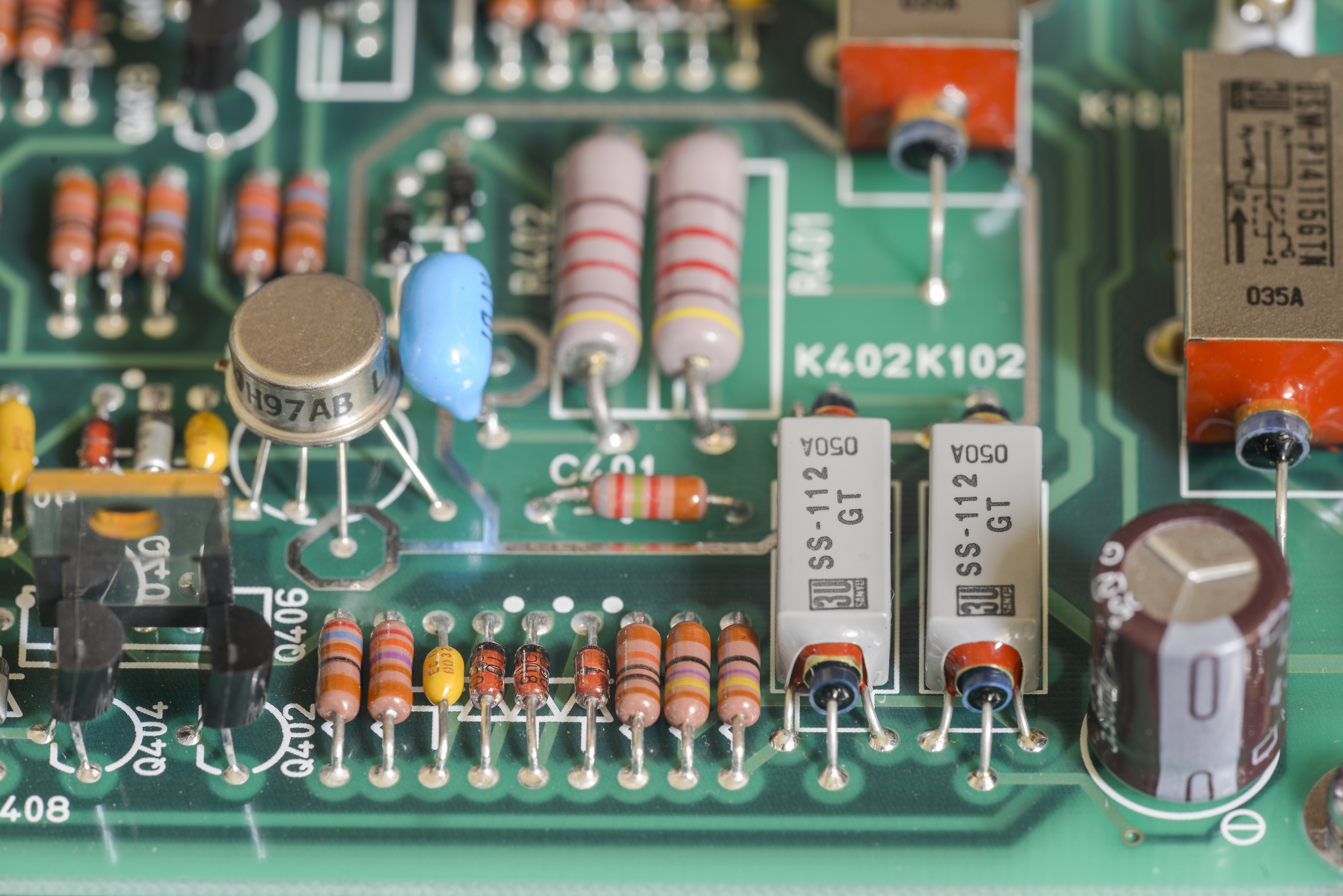
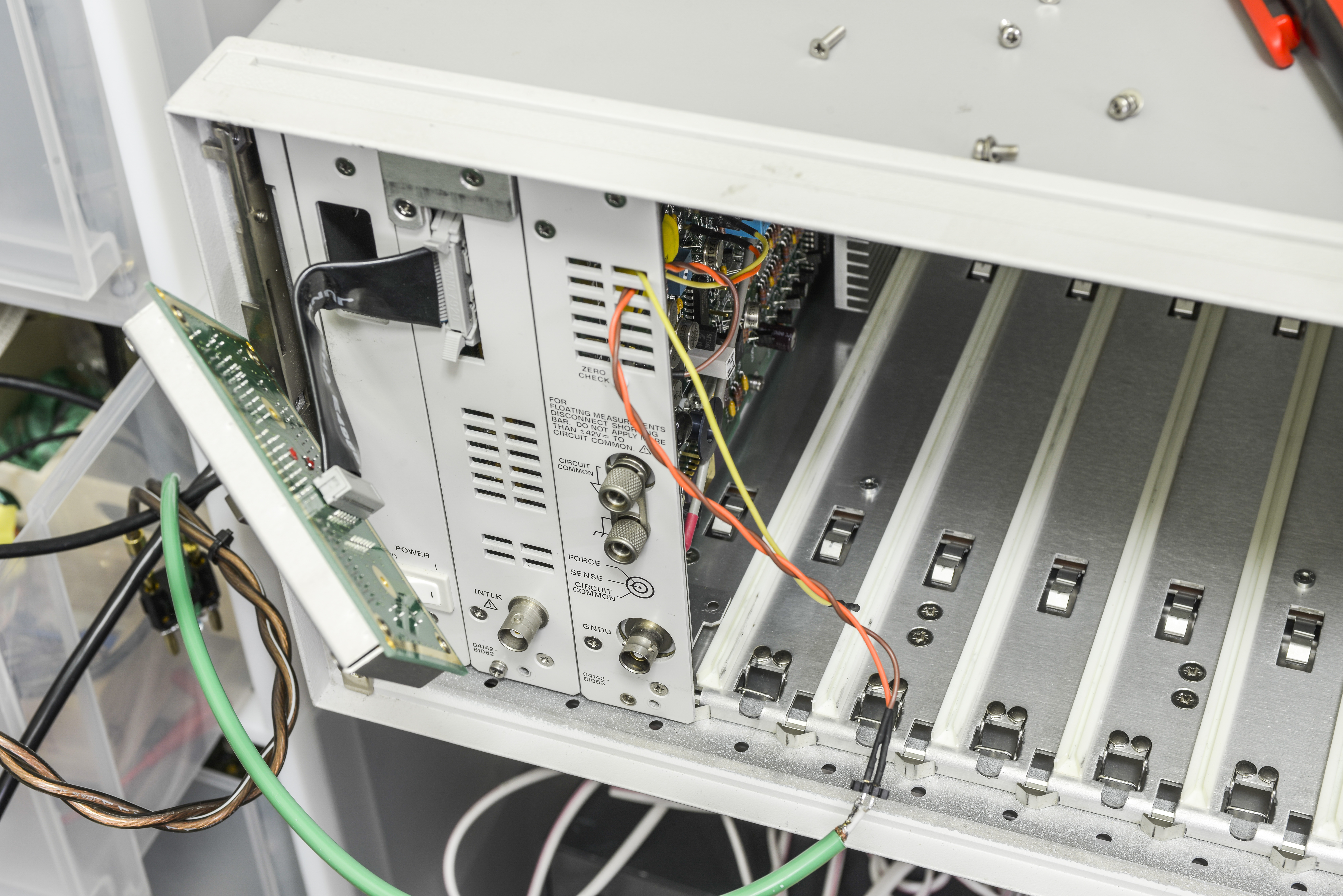
HP GNDU/ADC module
This module provides main analog functions of the mainframe, contain system-wide primary 10V reference, ADC and zero voltage high-current SMU able to sink 1.6A to force reference level at constant.
Large aluminum heatsink visible on the front side aided for proper thermal managment of the module.
Block diagram
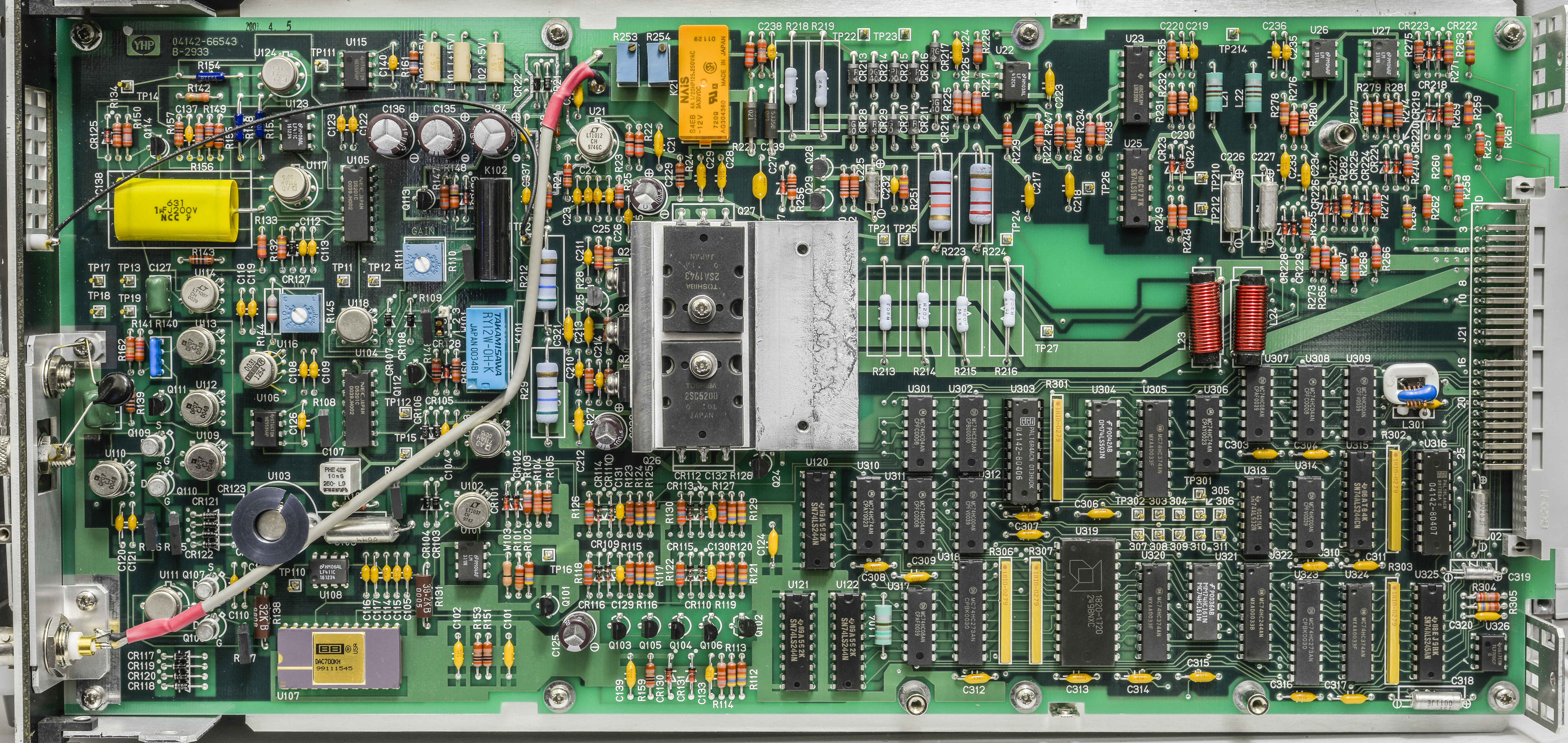
This heatsink was removed for clarify of the pictures. It couples to transistor cooling block via thermal paste.

Voltage reference U106 is 10V low-tempco 2.5ppm/°C Burr-Brown/TI REF102CM in hermetic (today obsolete) TO-99 package. This is best grade REF102, with maximum voltage error 2.5mV and long term stability 5ppm/1000hr. Reference date code is 0034, meaning 34 week of 2000.
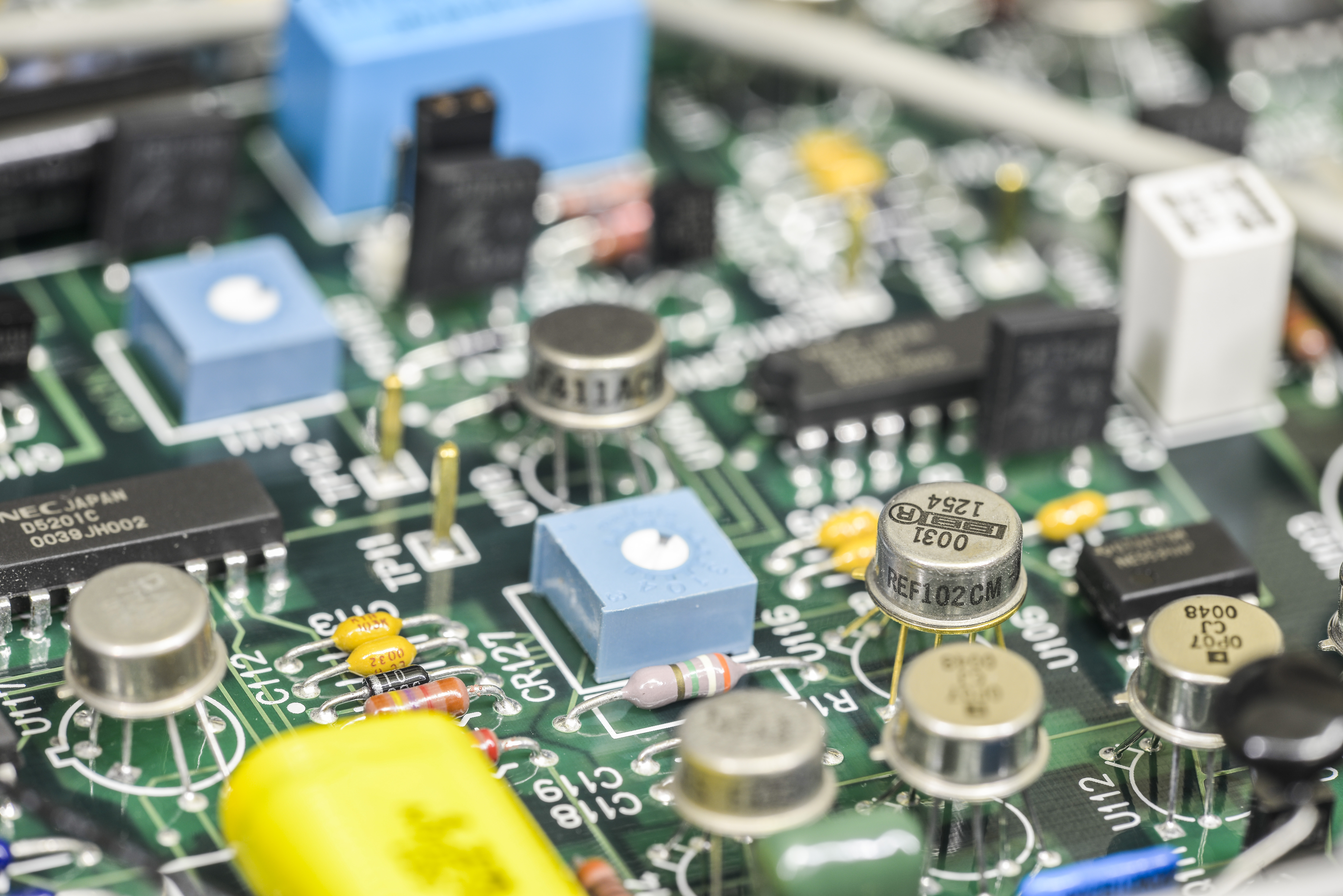
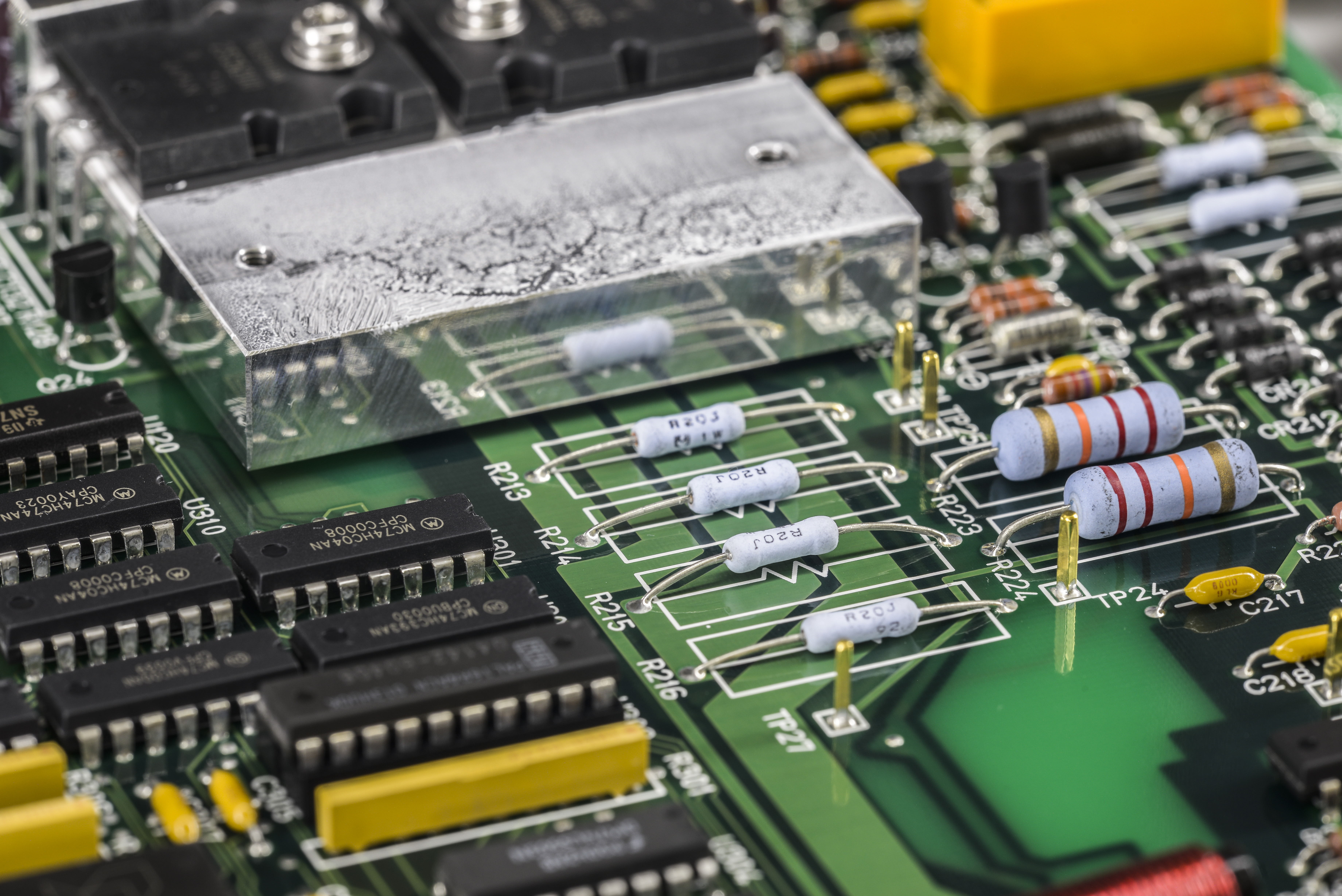
There are whole lot of operational amplifiers around in metal can hermetic packages. Some of precision foil resistors, manufactured by japanese vendor AE (now part of Vishay Precision Group) in square rectangular packages.
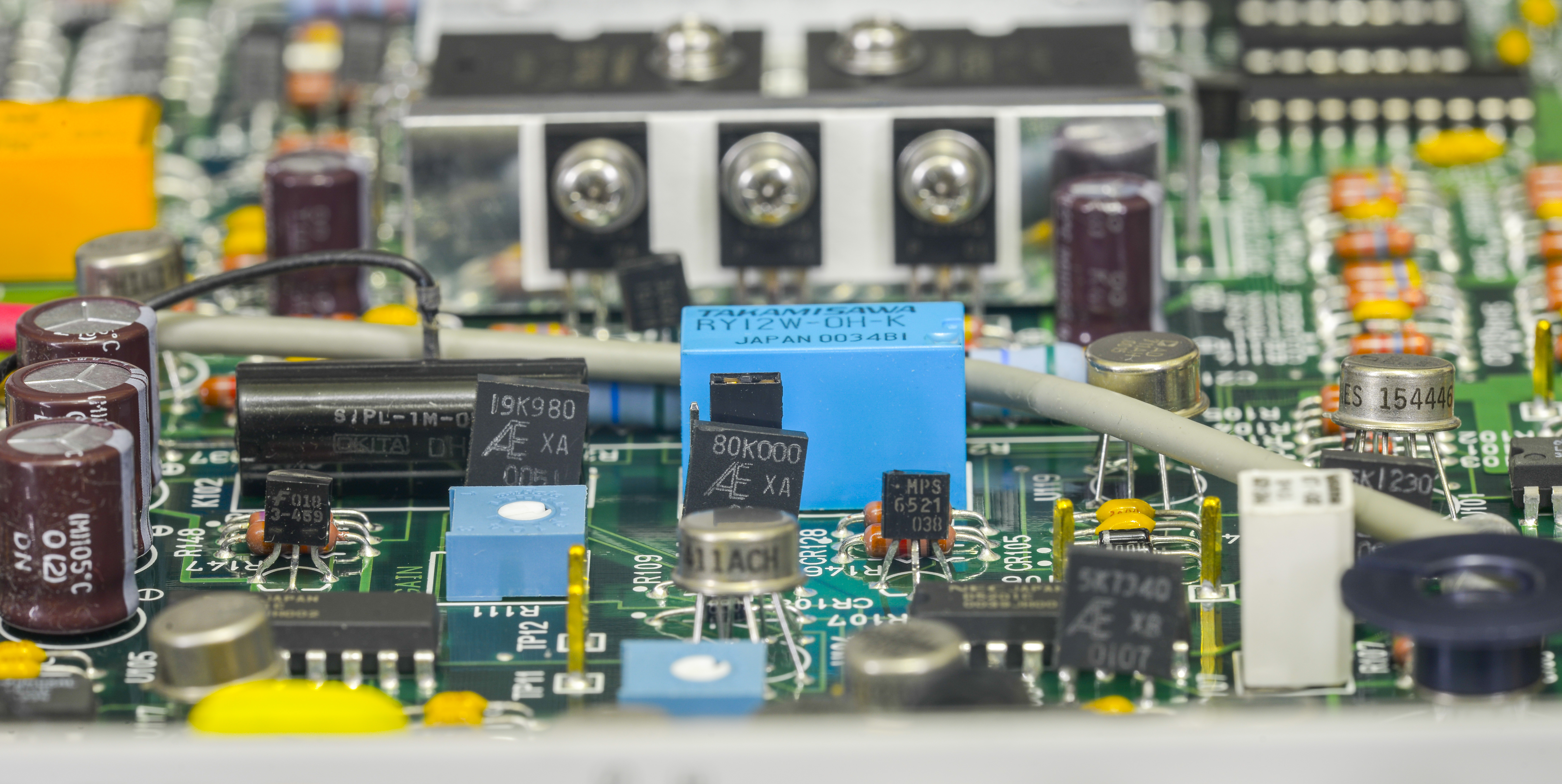
Here’s table of used precision resistors.
| RefDes | _ Resistor Type | Value |
|---|---|---|
| R136 | AE XA | 8.0000 KΩ |
| R135 | AE XQ | 40.000 KΩ |
| R108 | AE XB | 5.7340 KΩ |
| R106 | AE XA | 5.1230 KΩ |
| R109 | AE XA | 80.000 KΩ |
| R137 | AE XB | 16.000 KΩ |
| R110 | AE XA | 19.980 KΩ |
| R140 | AE 0L1 | Network 4 pin |

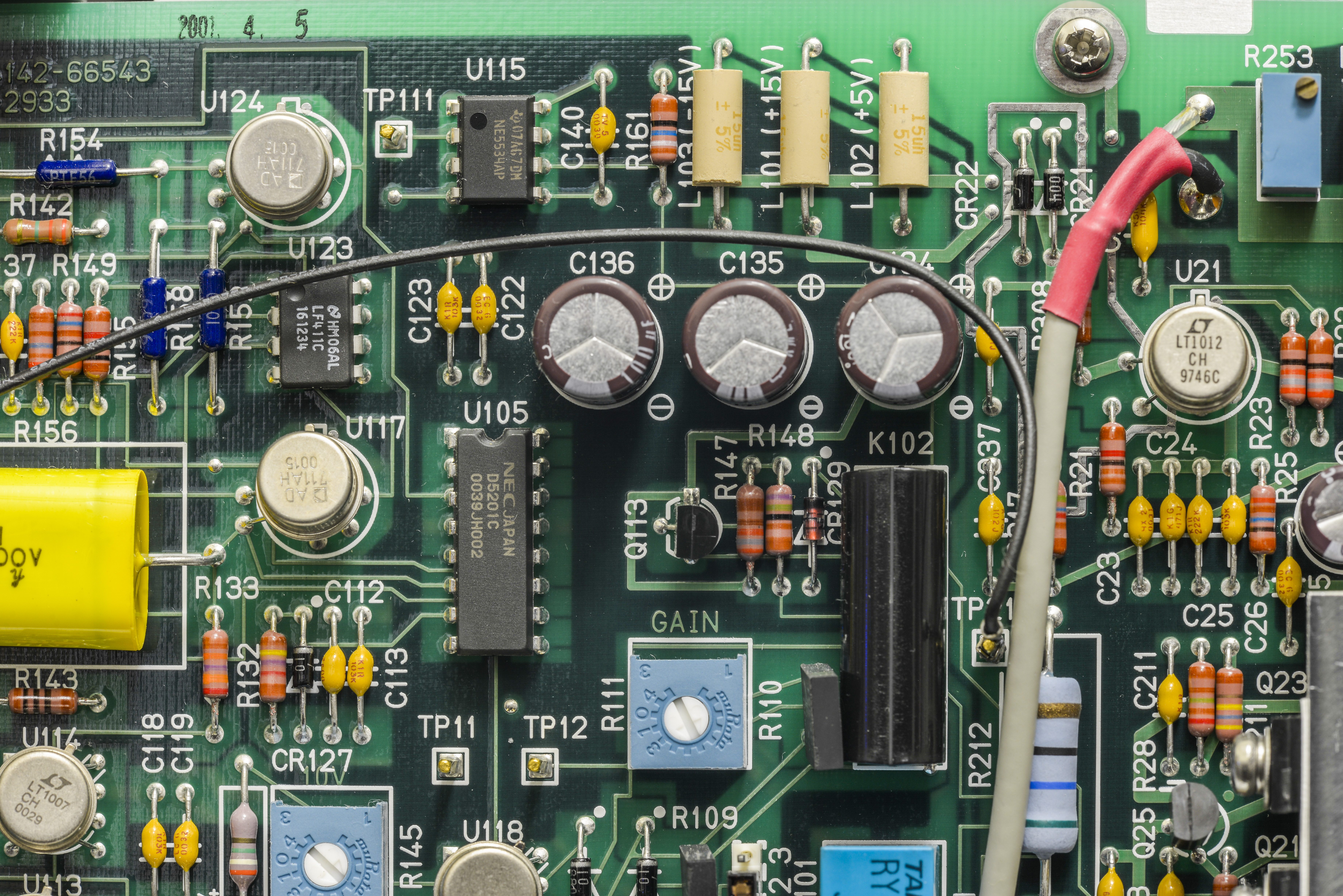
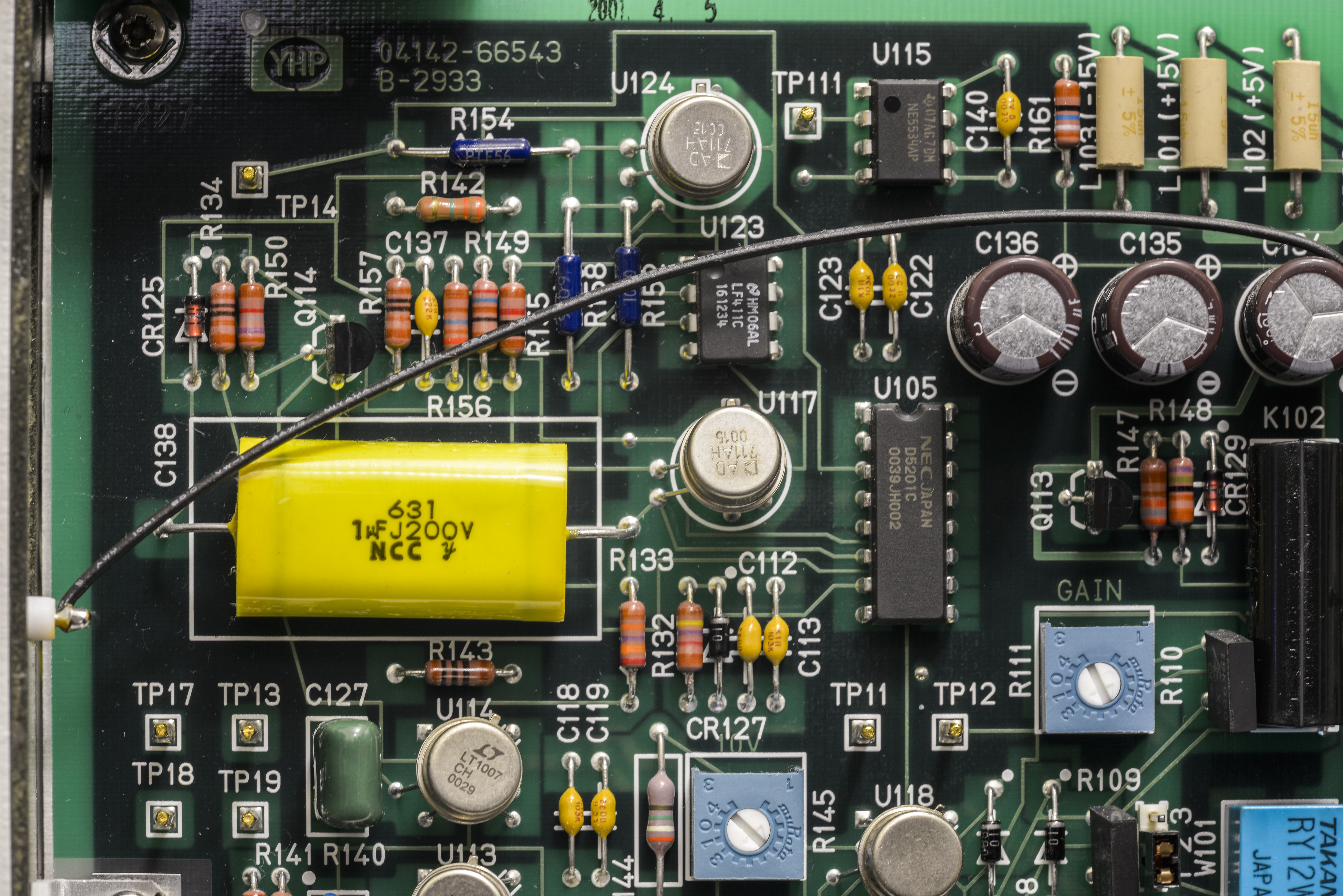
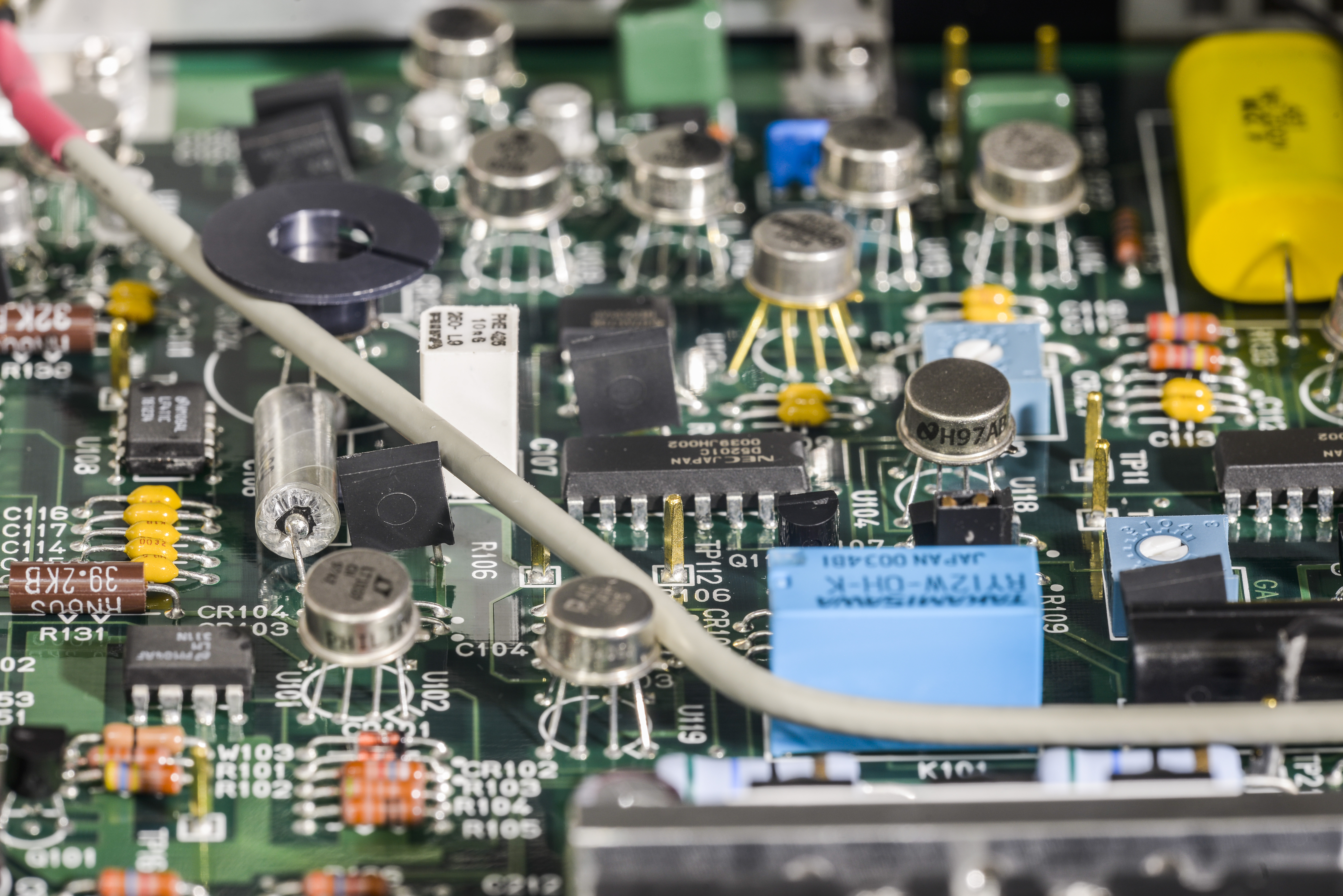
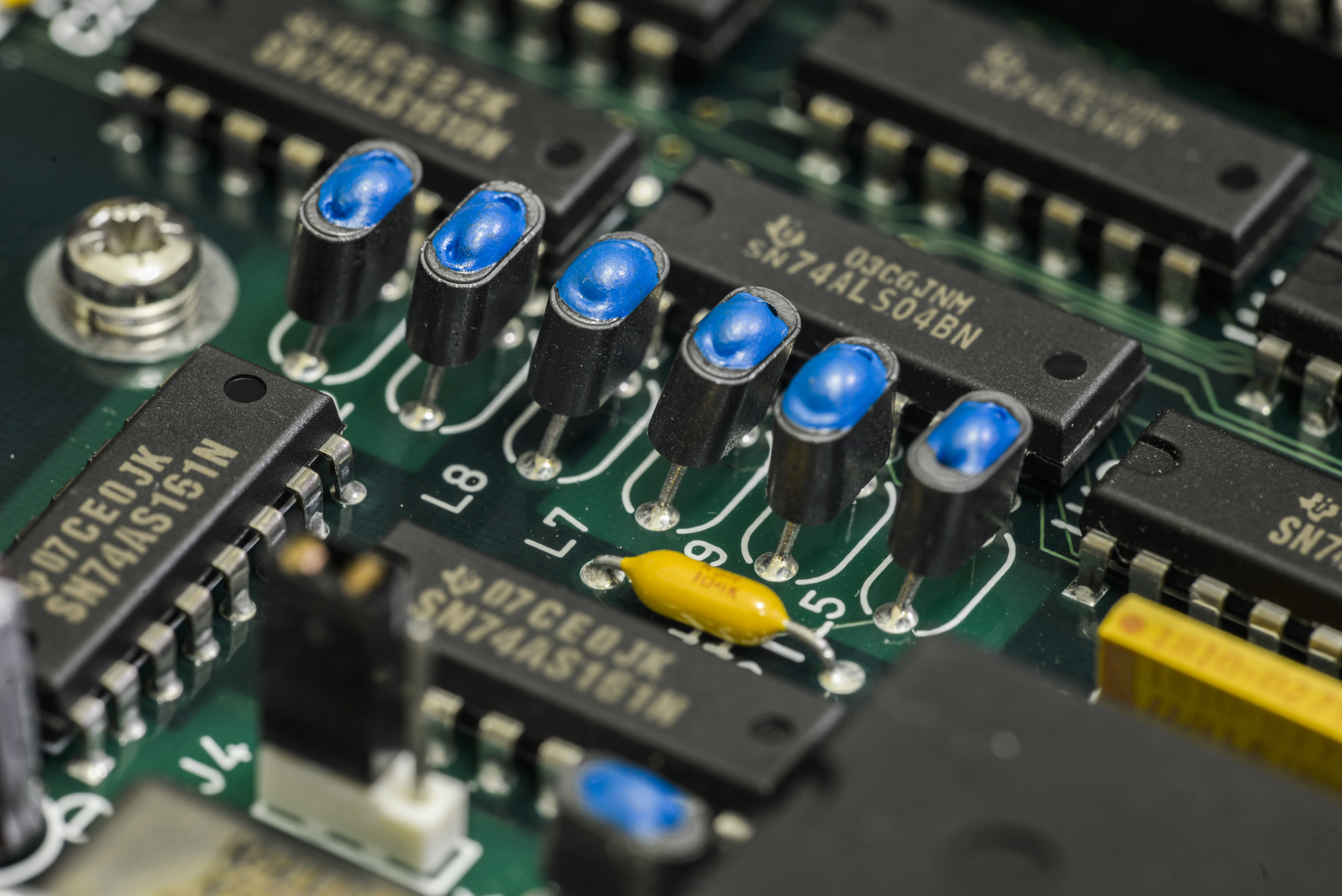
There are some custom AMD logic chips, bunch of 74-series logic and PAL16L8, surrounded by test points.
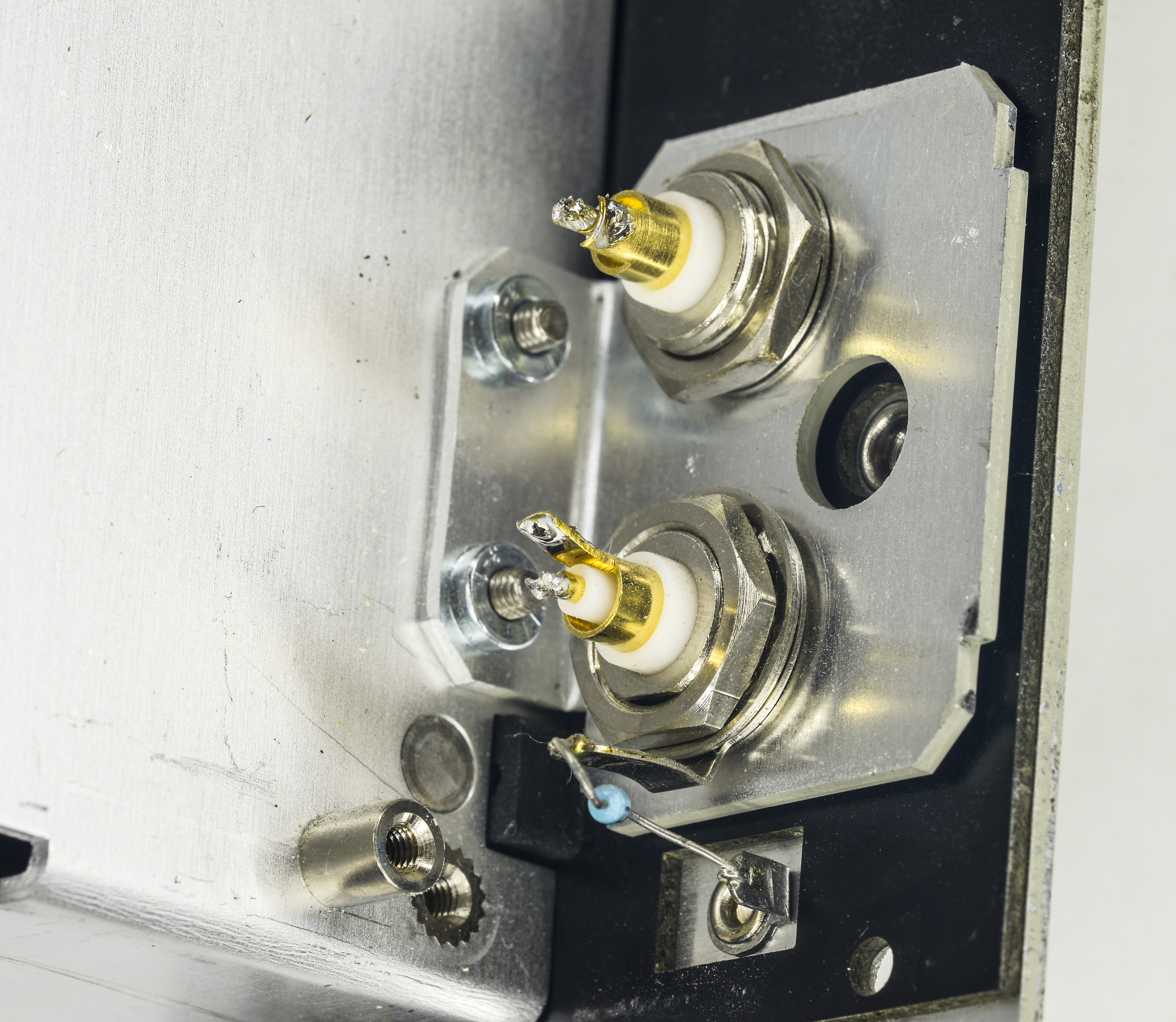
Front triaxial connector and circuit common fixed on solid aluminum plate tied to module high-power front end plane.
Module PCB marked with YHP logo. May that not confuse you, since Hewlett-Packard and Yokogawa had a joint venture (Yokogawa-Hewlett-Packard) in 1963 to market and sell HP products in Japan. HP later bought it’s Yokogawa Electric share in 1999. That also explains why majority of components in this 4142B are made in Japan.
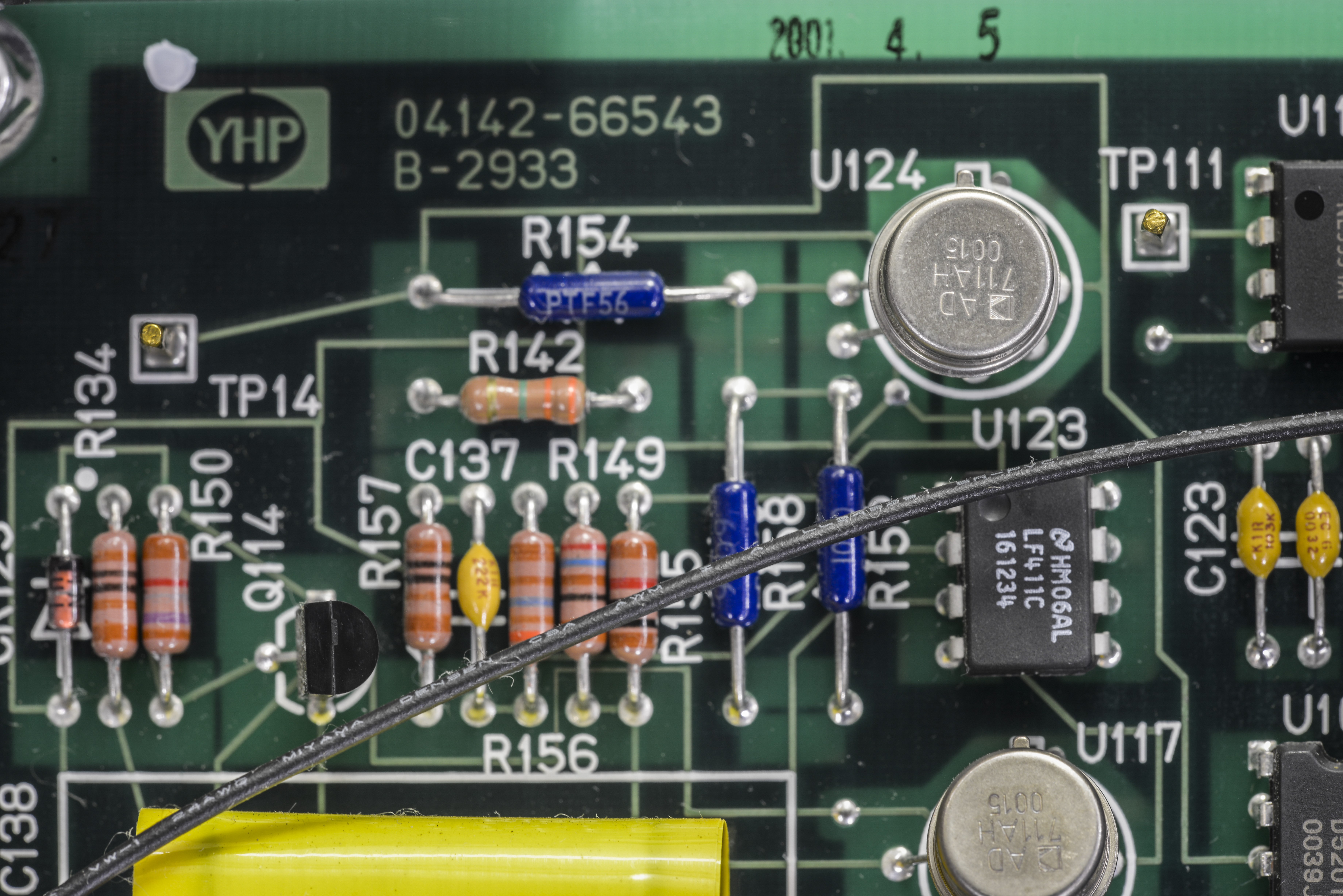
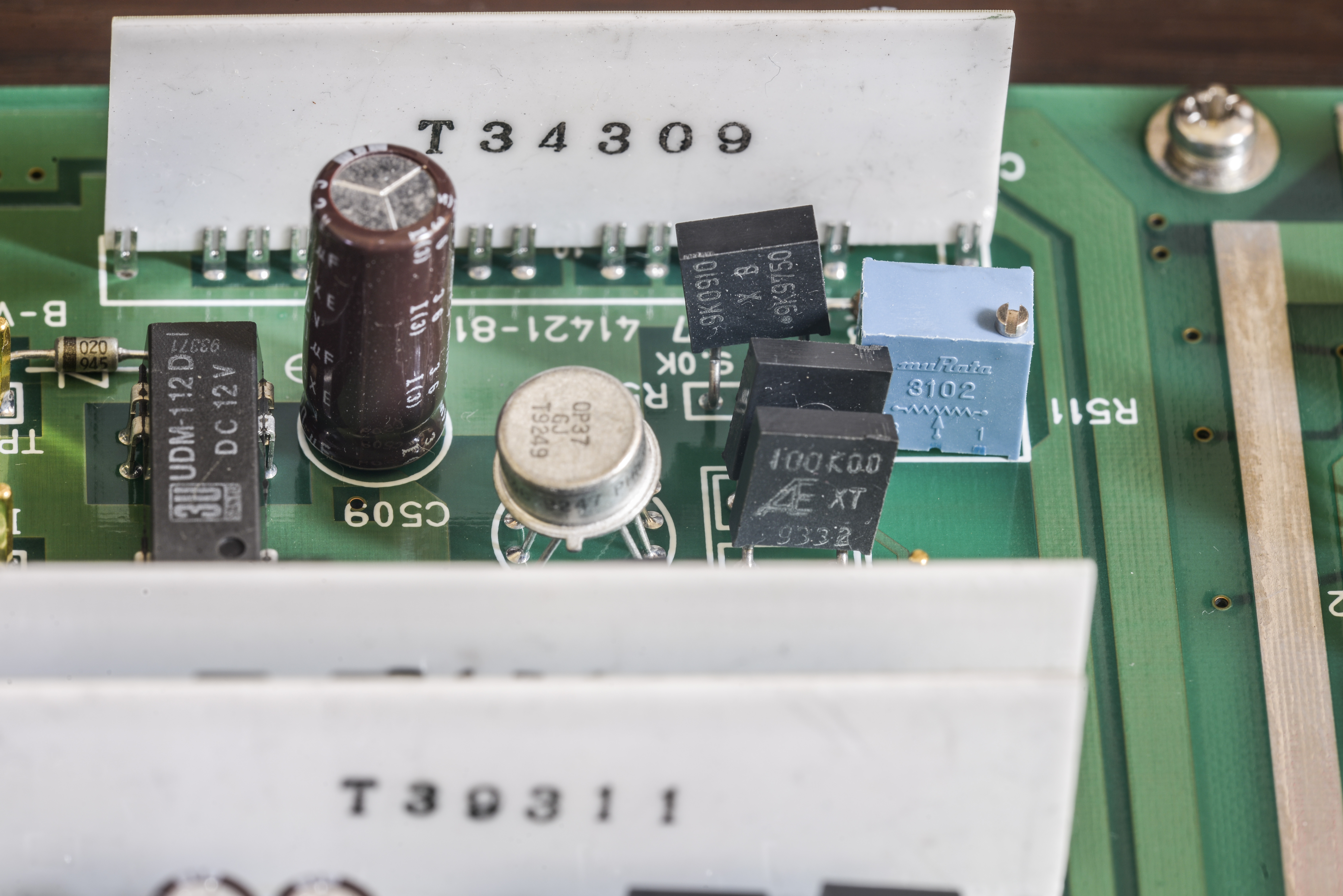
Board features dozen of trim resistors for calibration and adjustment purposes.

Triaxial port connected by coaxial wire runnin all over the board to the output relay location.


ADC is interesting SAR-type solution with 17-bit feedback DAC, combined from use of 16-bit ladder R2R monolithic Burr-brown DAC700KH and onboard discrete circuitry to get extra bit. This precision DAC chip have maximum linearity error 30ppm of FSR. DAC chip is using ceramic hermetic DIP, no expense was saved to ensure unit specs. This DAC is also very fast, specified with 1µS settling time into 100Ω load.
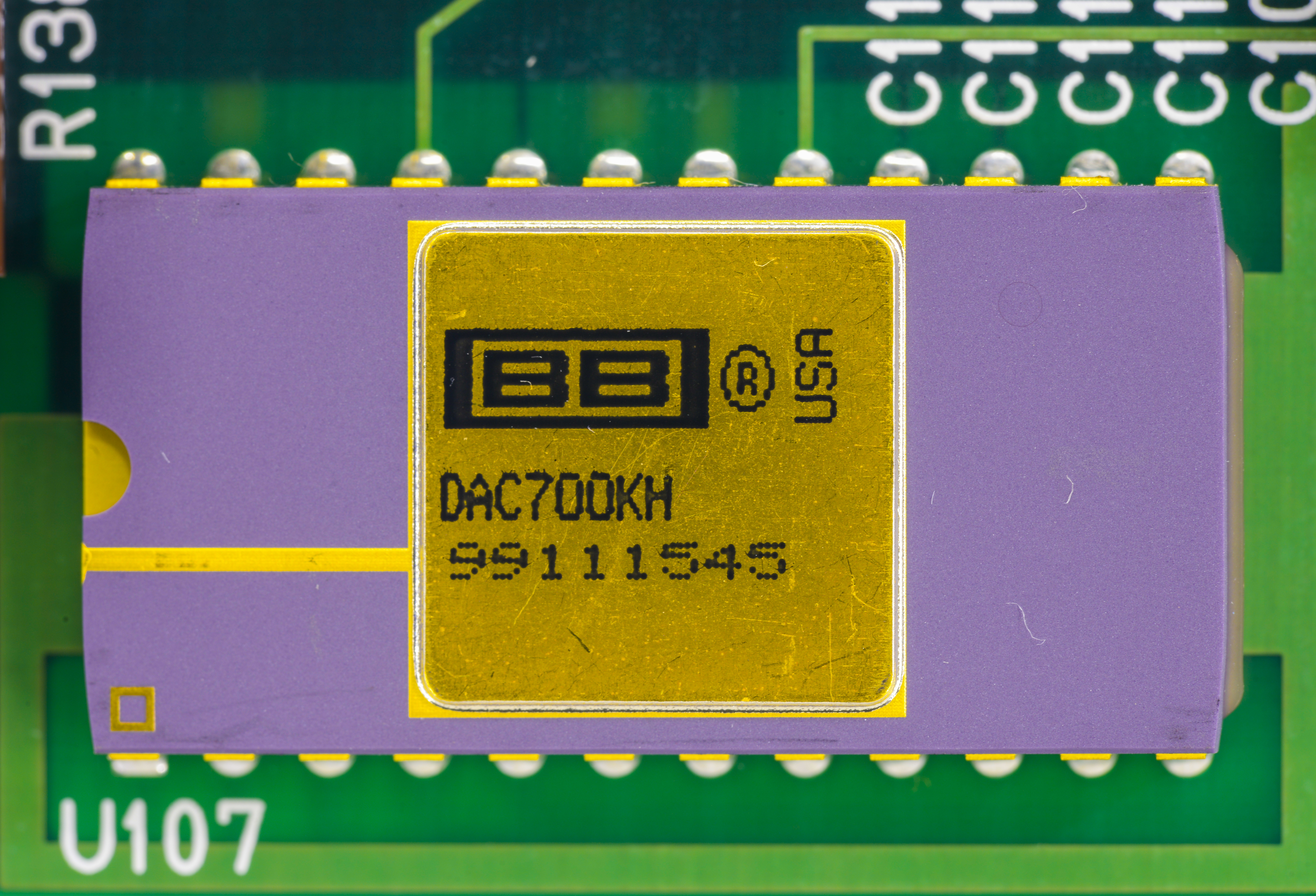
DAC700 have current output only, from 0 to -2 mA with typical output impedance 4kΩ. It’s also have it’s own buried zener +6.3V voltage reference with ±25ppm/°C tempco.
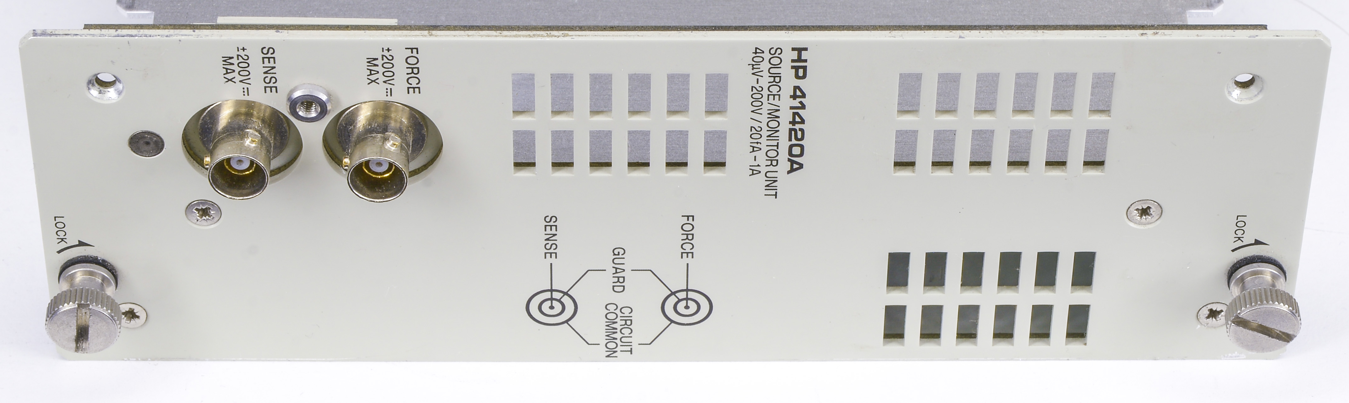
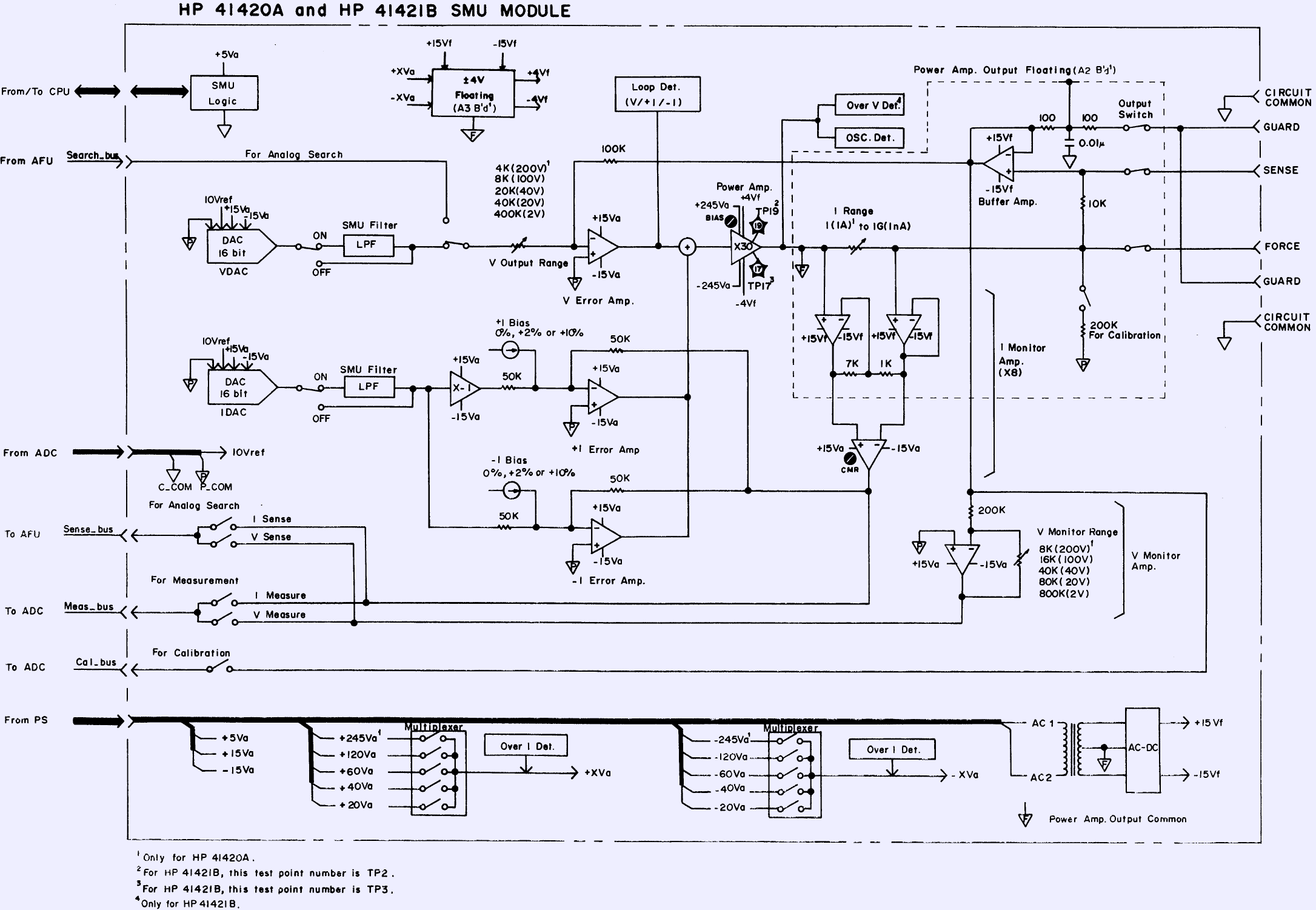
HP 41420A HPSMU High-power Source/Monitor 200V/1A Unit
This module takes 2 slots in 4142B.
Block diagram
I got one broken HPSMU module as well. Diagnostics and repair will be performed later.
| Function | Output | Resolution | Max load | Accuracy |
|---|---|---|---|---|
| Voltage source/measure | -2.0000 … 2.0000 V | 40 µVDC | 1 A | ±0.05% + 1mV |
| Voltage source/measure | -20.000 … 20.000 V | 400 µVDC | 1 A (0.7A) | ±0.05% + 10mV |
| Voltage source/measure | -40.000 … 40.000 V | 800 µVDC | 0.35 A | ±0.05% + 20mV |
| Voltage source/measure | -100.00 … 100.00 V | 2 mVDC | 125 mA | ±0.05% + 50mV |
| Voltage source/measure | -200.00 … 200.00 V | 4 mVDC | 50 mA | ±0.05% + 100mV |
| Current source/measure | -1.0000 … 1.0000 nA | 20 fA | ±200V | ±1% + 6pA + 20fA × VOUT |
| Current source/measure | -10.000 … 10.000 nA | 200 fA | ±200V | ±1% + 15pA + 200fA × VOUT |
| Current source/measure | -100.00 … 100.00 nA | 2 pA | ±200V | ±0.5% + 100pA + 2pA × VOUT |
| Current source/measure | -1.0000 … 1.0000 µA | 20 pA | ±200V | ±0.5% + 1nA + 20pA × VOUT |
| Current source/measure | -10.000 … 10.000 µA | 200 pA | ±200V | ±0.2% + 10nA + 200pA × VOUT |
| Current source/measure | -100.00 … 100.00 µA | 2 nA | ±200V | ±0.2% + 100nA + 2nA × VOUT |
| Current source/measure | -1.0000 … 1.0000 mA | 20 nA | ±200V | ±0.2% + 1µA + 20nA × VOUT |
| Current source/measure | -10.000 … 10.000 mA | 200 nA | ±200V | ±0.2% + 10µA + 200nA × VOUT |
| Current source/measure | -100.00 … 100.00 mA | 2 µA | ±100V | ±0.2% + 100µA + 2µA × VOUT |
| Current source/measure | -1.0000 … 1.0000 A | 20 µA | ±200-14V | ±0.5% + 1mA + 20µA × VOUT |
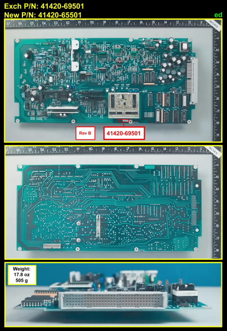
Module board photo from Keysight Find-A-Part site:
“
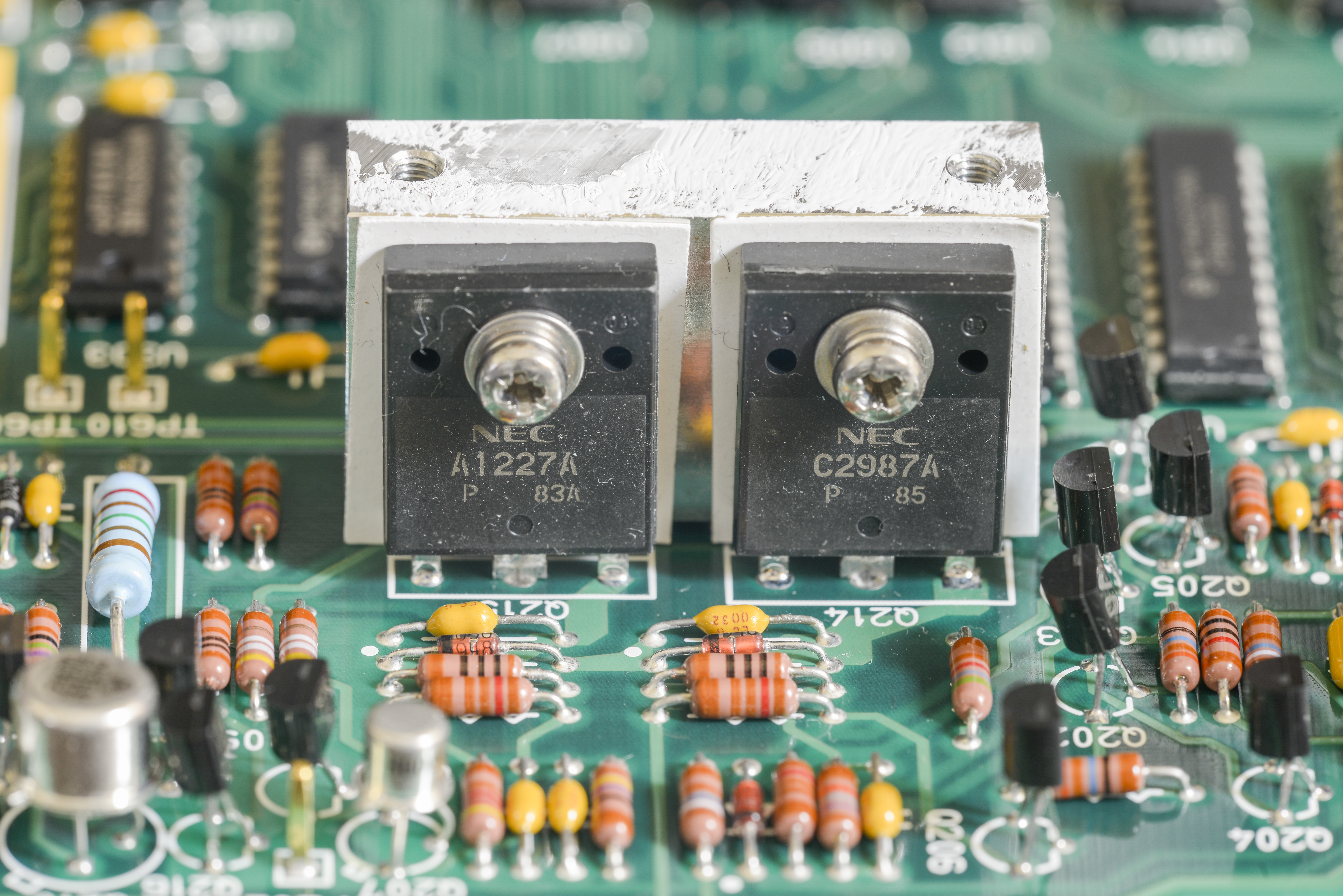
This module have an issue and fails self-diagnostics. Error code is 423 which according to service manual decodes as issue with I monitor opamp on output board A2. Time to open module for initial photos and diagnostics.
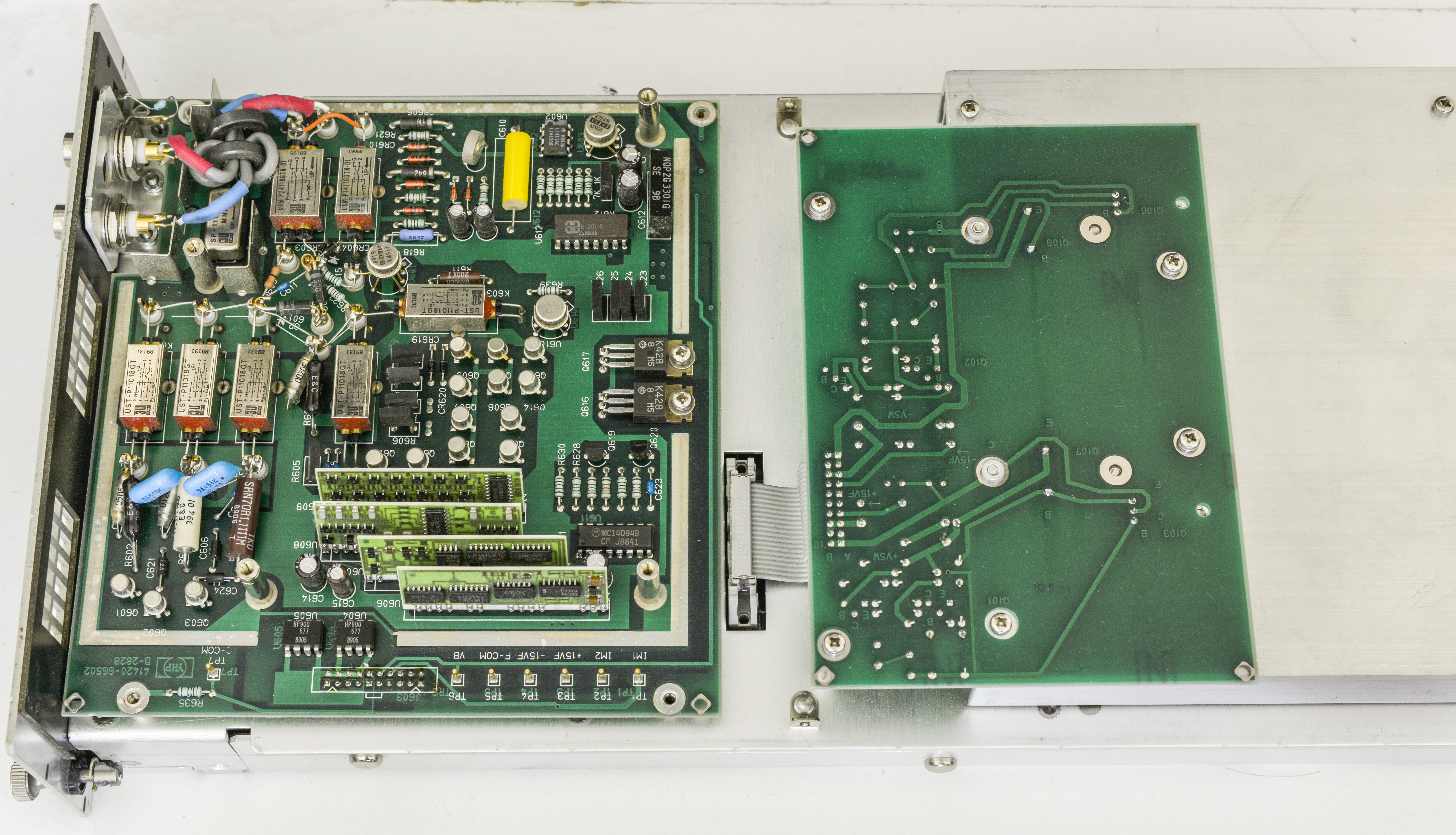
There are still flux residue on reed relay pins, but that should not be a reason of SMU’s failure.

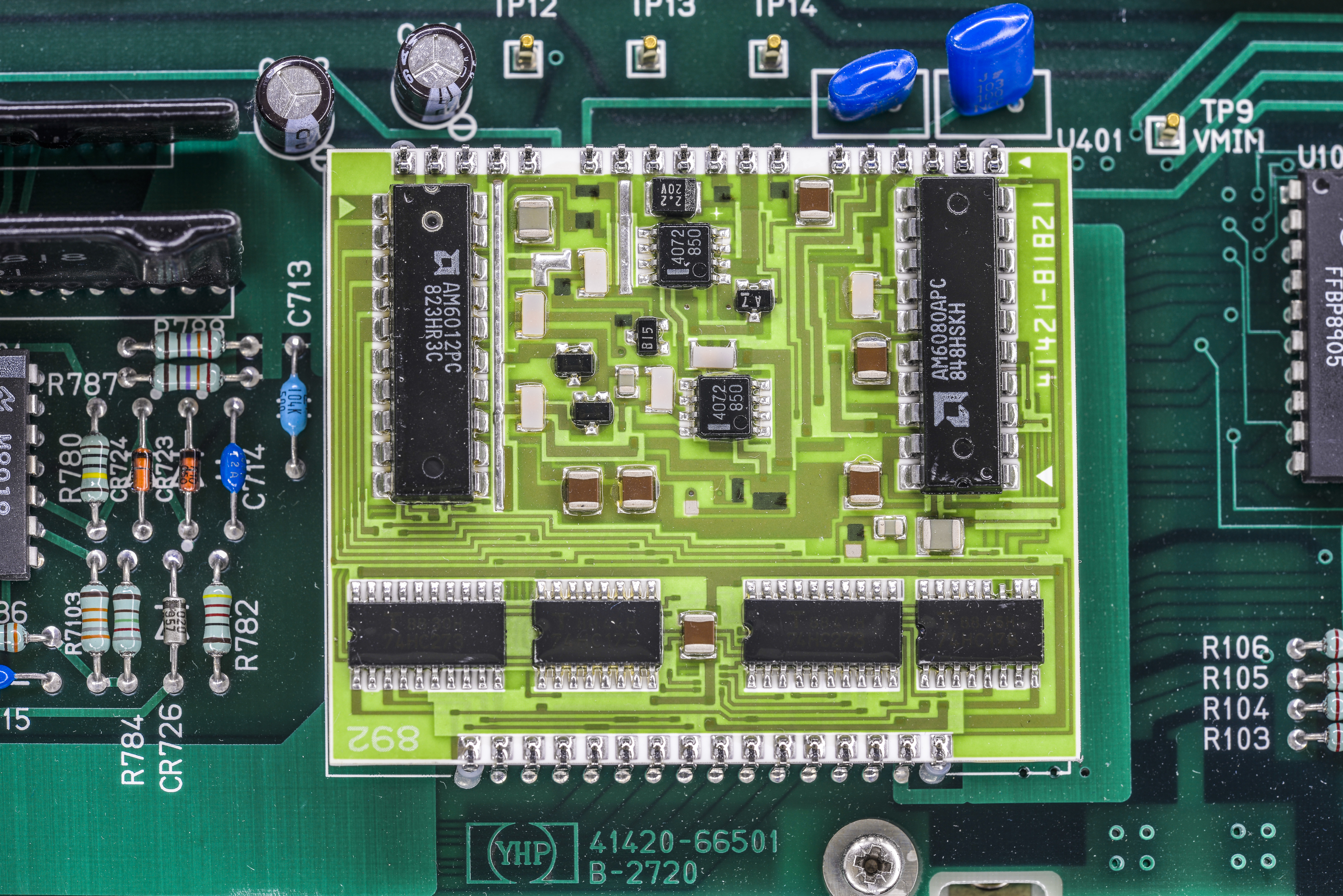
DAC ceramic hybrid is same as one used in HP/Agilent 41421B as we will see later. It consists of 12-bit AMD AM6012PC DAC and 8-bit AM6080APC DAC and some control logic to drive control signals of both DAC in sync.
More NEC green transistors, made in Japan.
And of course more hybrids.
Most of hybrids are dual layer with some film laser-trimmed resistors.

Triaxial output and wiring
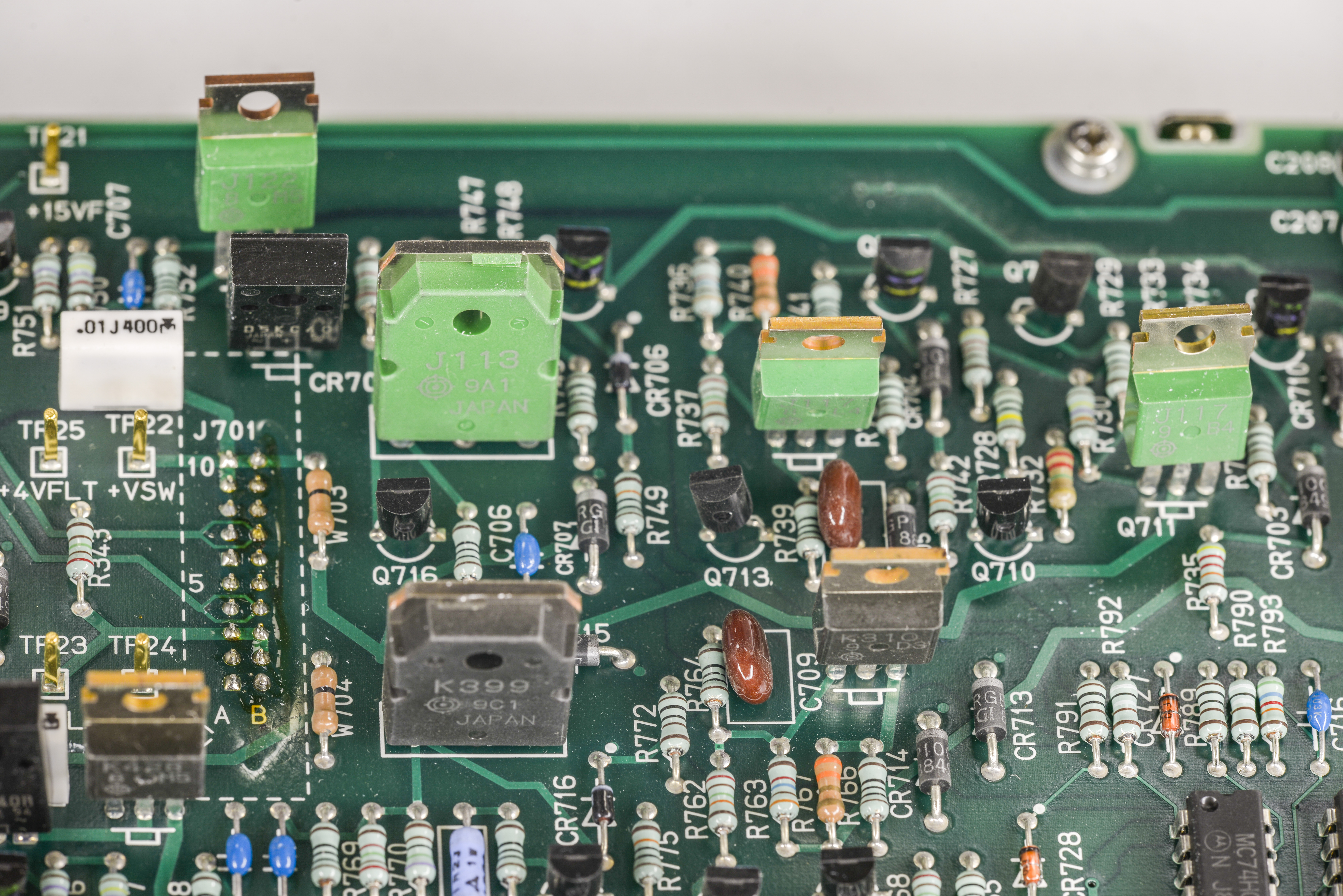
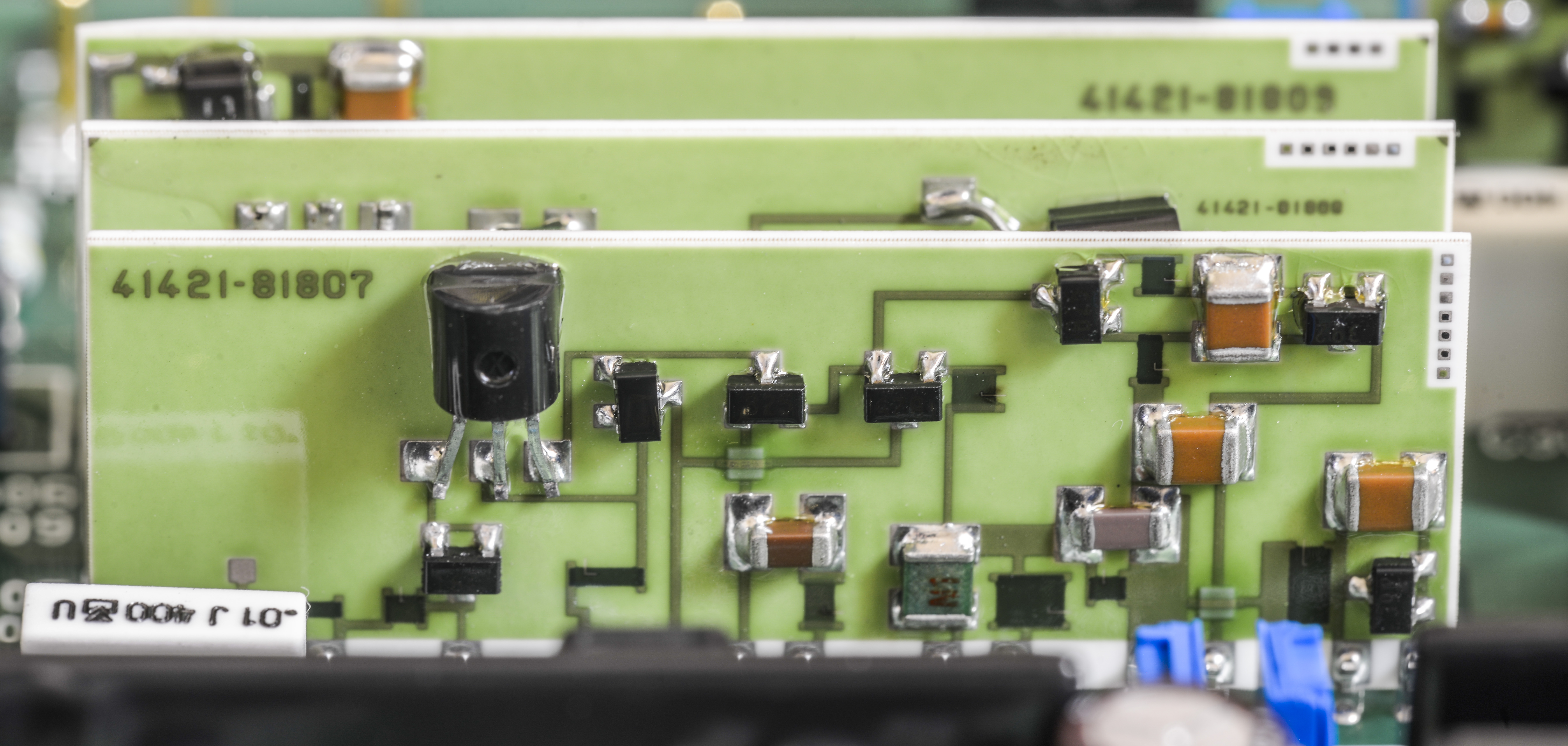
HP 41421A MPSMU Medium-power Source/Monitor 100V/100mA Unit
This module takes 1 slot in 4142B. Block diagram is exactly same as 41420A with exception of circuitry for 200V and 1A ranges.
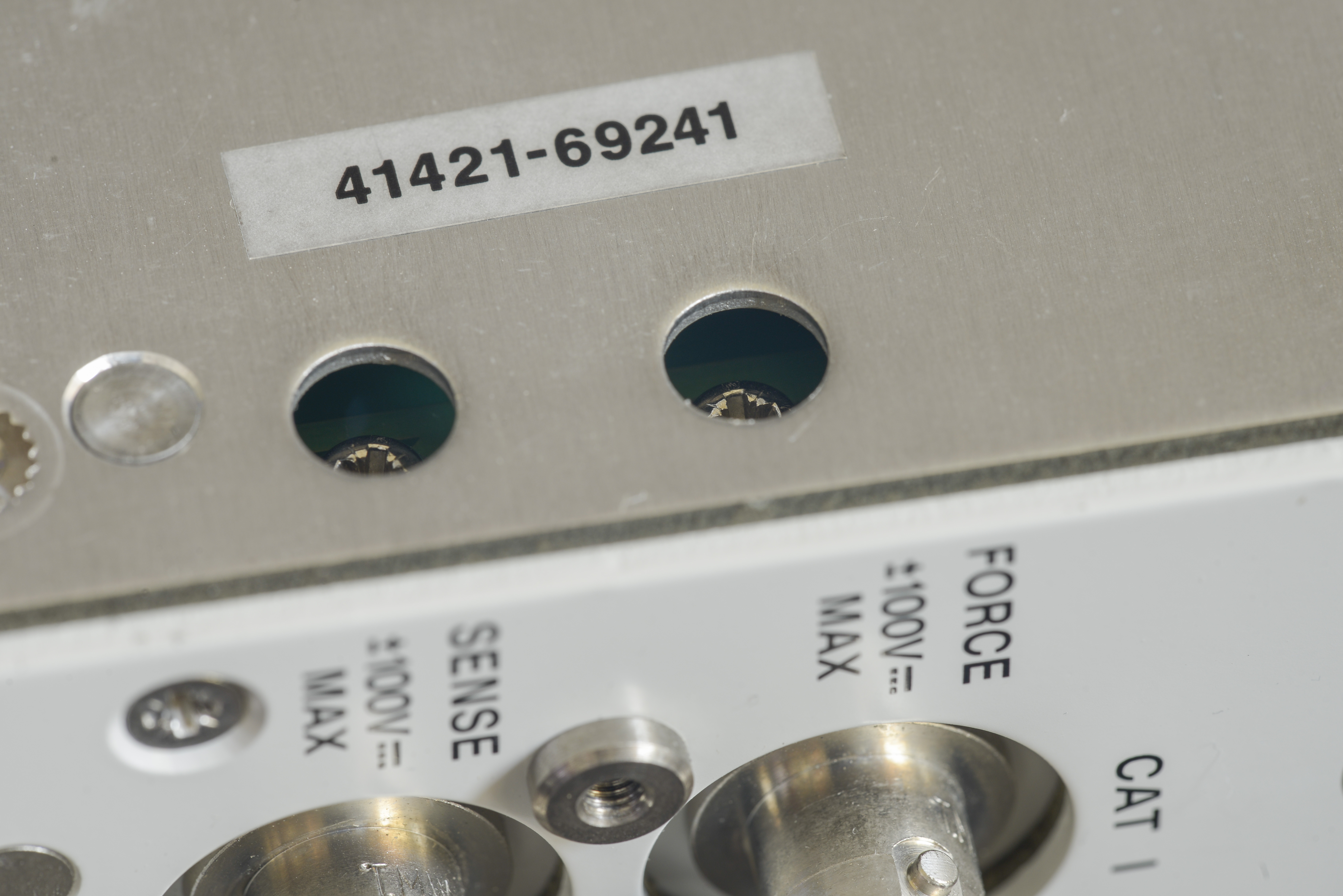
Both force and sense terminals are guarded and implemented via 3-lug triaxial TRX connector.
| Function | Output | Resolution | Max load | Accuracy |
|---|---|---|---|---|
| Voltage source/measure | -2.0000 … 2.0000 V | 40 µVDC | ±100 mA | ±0.05% + 1mV |
| Voltage source/measure | -20.000 … 20.000 V | 400 µVDC | ±100 mA | ±0.05% + 10mV |
| Voltage source/measure | -40.000 … 40.000 V | 800 µVDC | ±50 mA | ±0.05% + 20mV |
| Voltage source/measure | -100.00 … 100.00 V | 2 mVDC | ±20 mA | ±0.05% + 50mV |
| Current source/measure | -1.0000 … 1.0000 nA | 20 fA | ±100V | ±1% + 6pA + 20fA × VOUT |
| Current source/measure | -10.000 … 10.000 nA | 200 fA | ±100V | ±1% + 15pA + 200fA × VOUT |
| Current source/measure | -100.00 … 100.00 nA | 2 pA | ±100V | ±0.5% + 100pA + 2pA × VOUT |
| Current source/measure | -1.0000 … 1.0000 µA | 20 pA | ±100V | ±0.5% + 1nA + 20pA × VOUT |
| Current source/measure | -10.000 … 10.000 µA | 200 pA | ±100V | ±0.2% + 10nA + 200pA × VOUT |
| Current source/measure | -100.00 … 100.00 µA | 2 nA | ±100V | ±0.2% + 100nA + 2nA × VOUT |
| Current source/measure | -1.0000 … 1.0000 mA | 20 nA | ±100V | ±0.2% + 1µA + 20nA × VOUT |
| Current source/measure | -10.000 … 10.000 mA | 200 nA | ±100V | ±0.2% + 10µA + 200nA × VOUT |
| Current source/measure | -100.00 … 100.00 mA | 2 µA | ±20V | ±0.2% + 100µA + 2µA × VOUT |
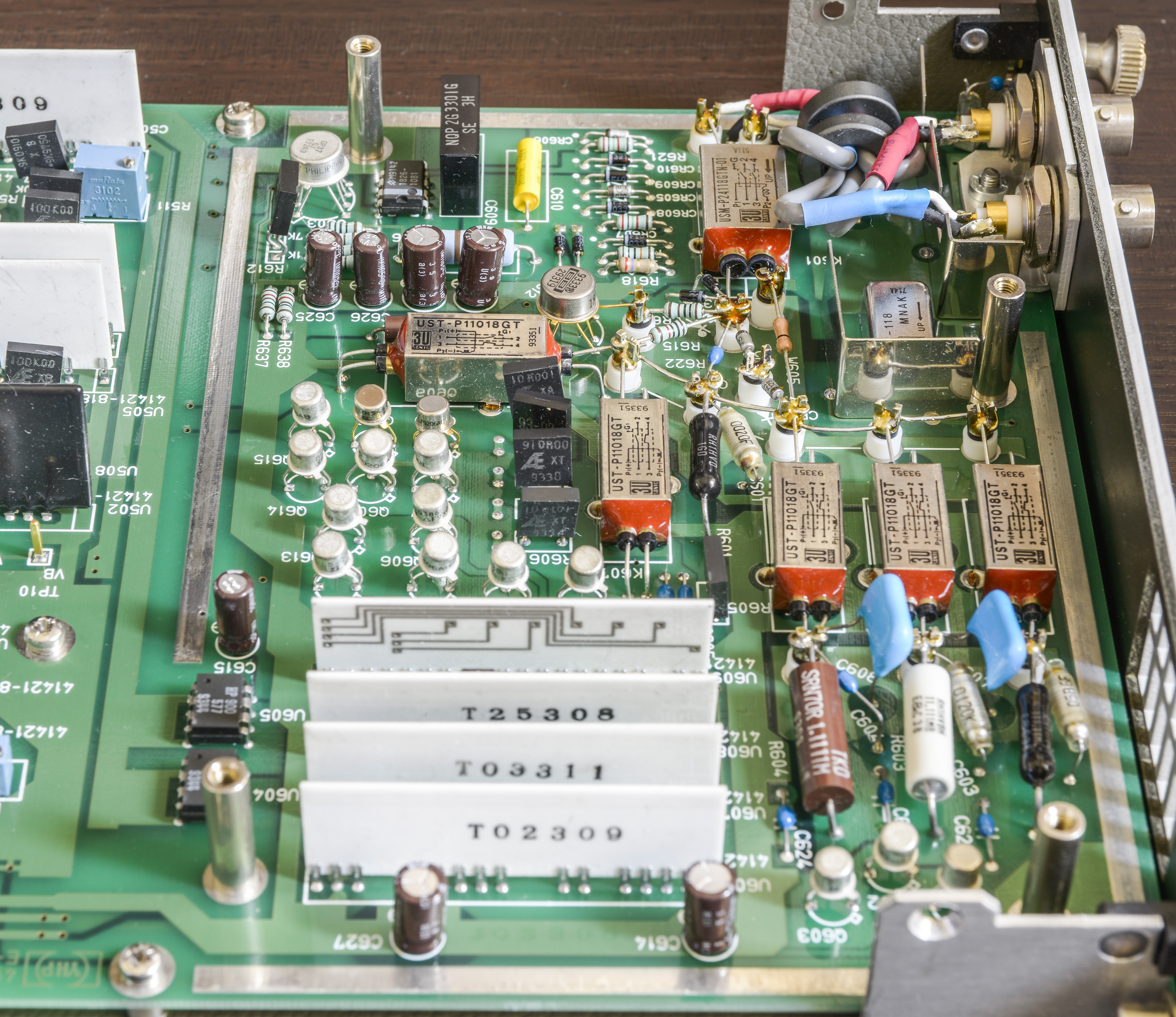
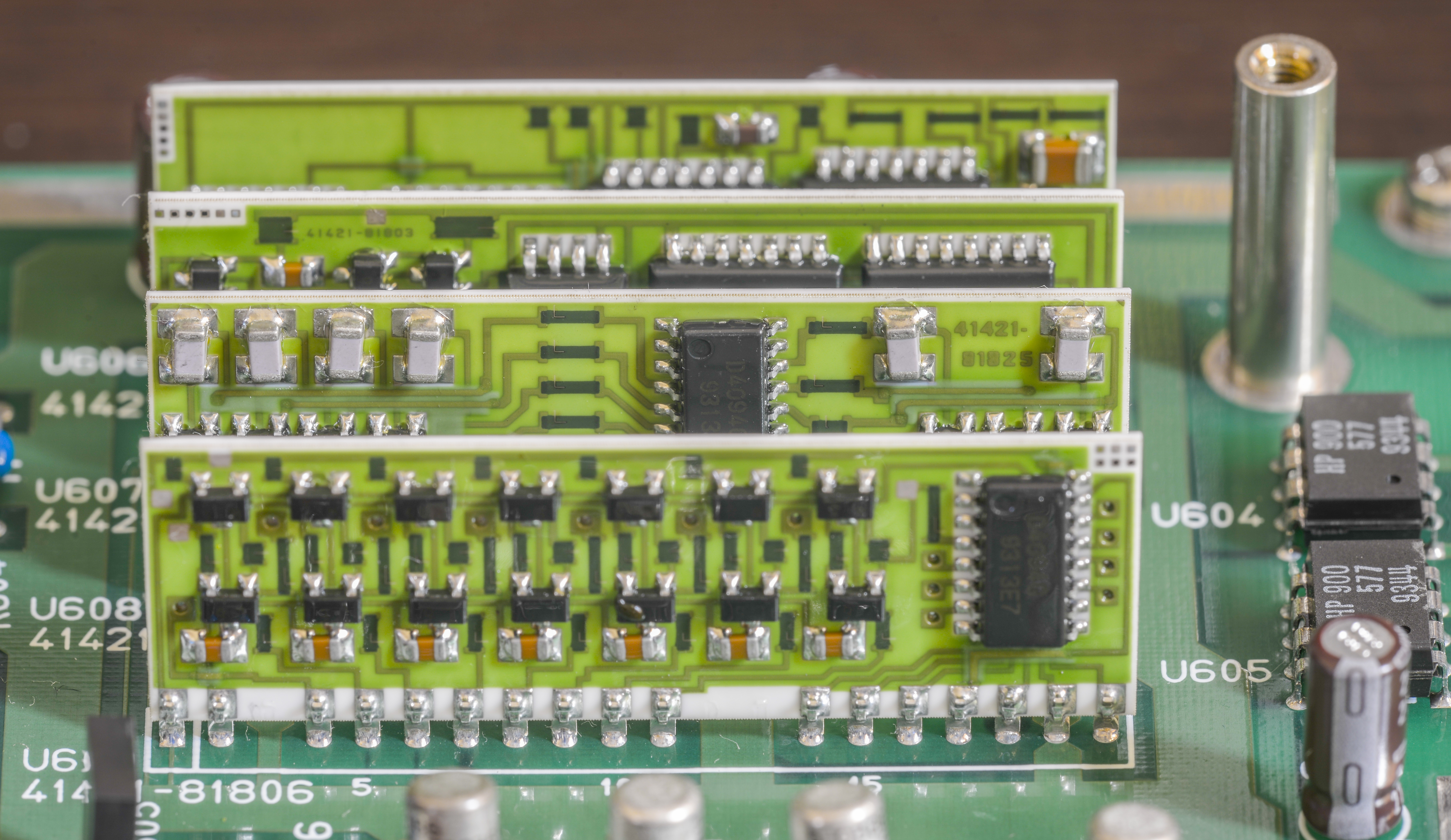
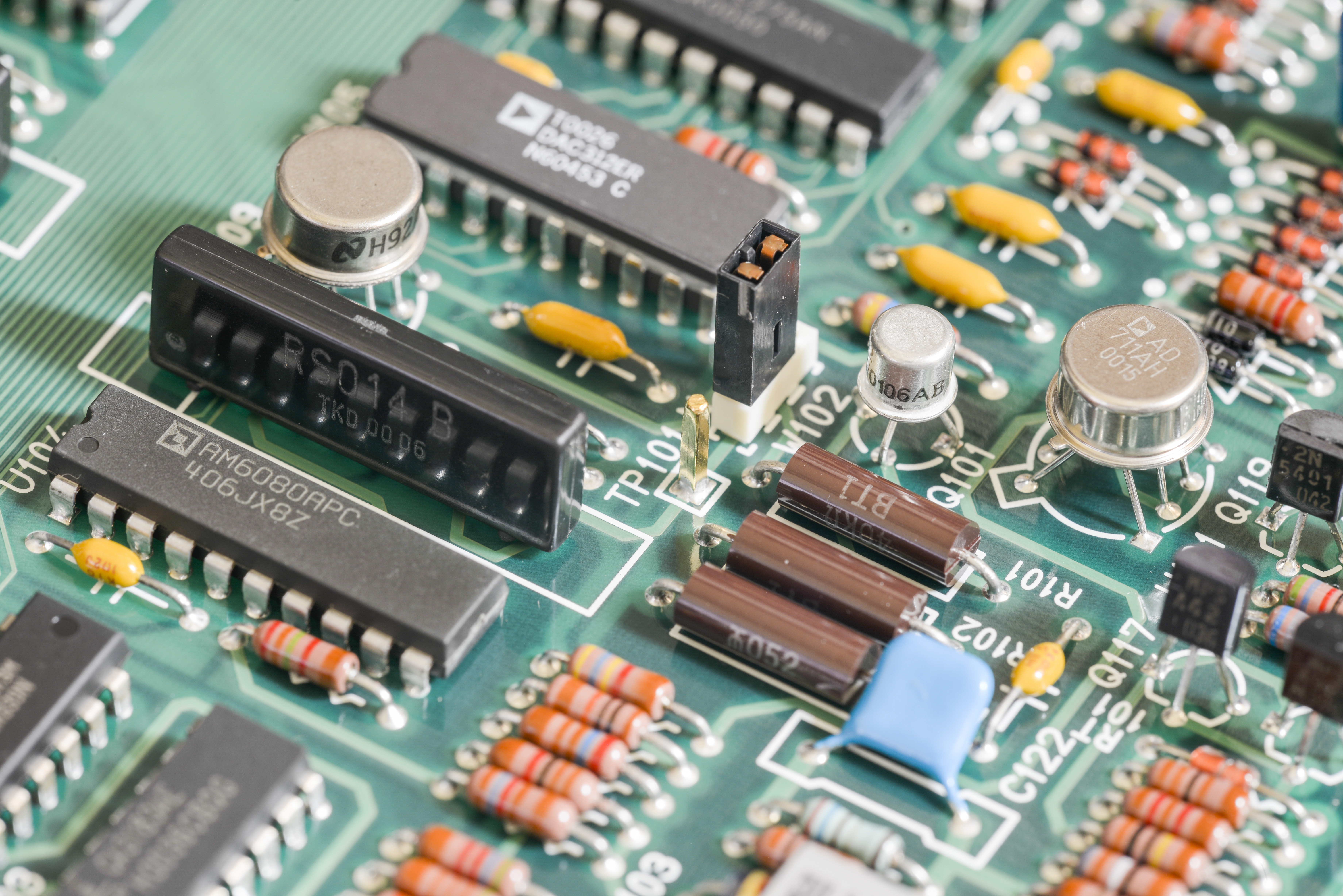
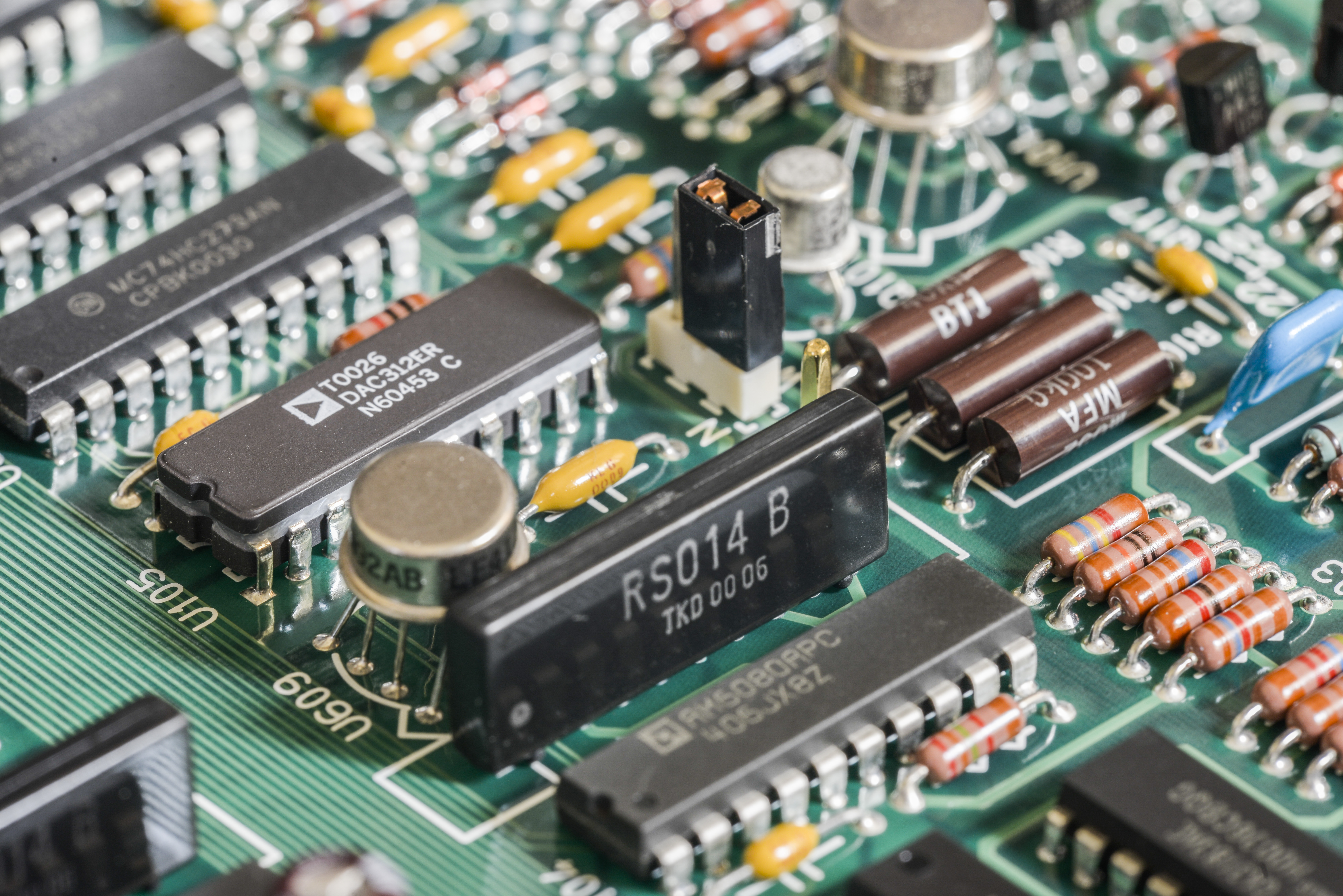
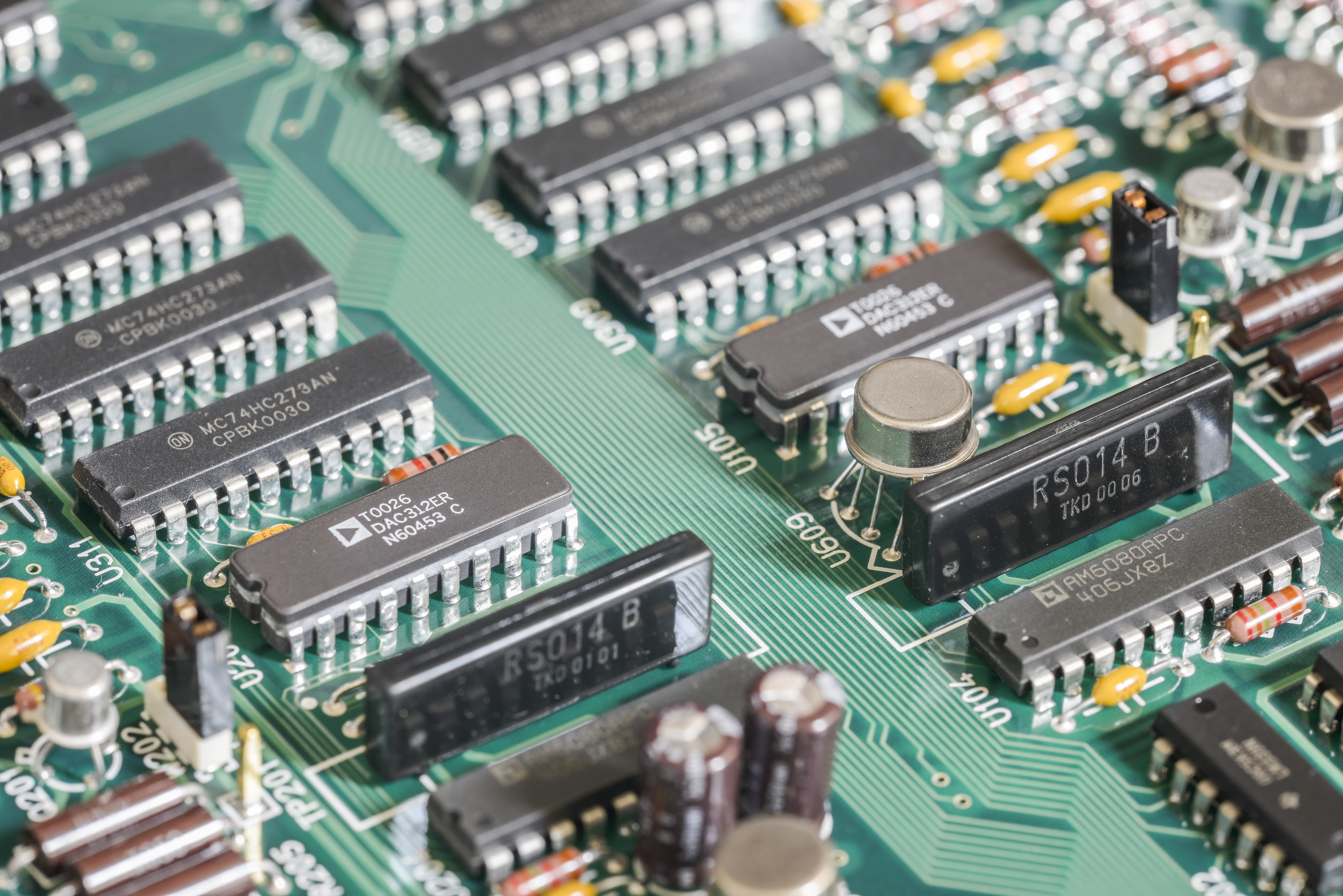
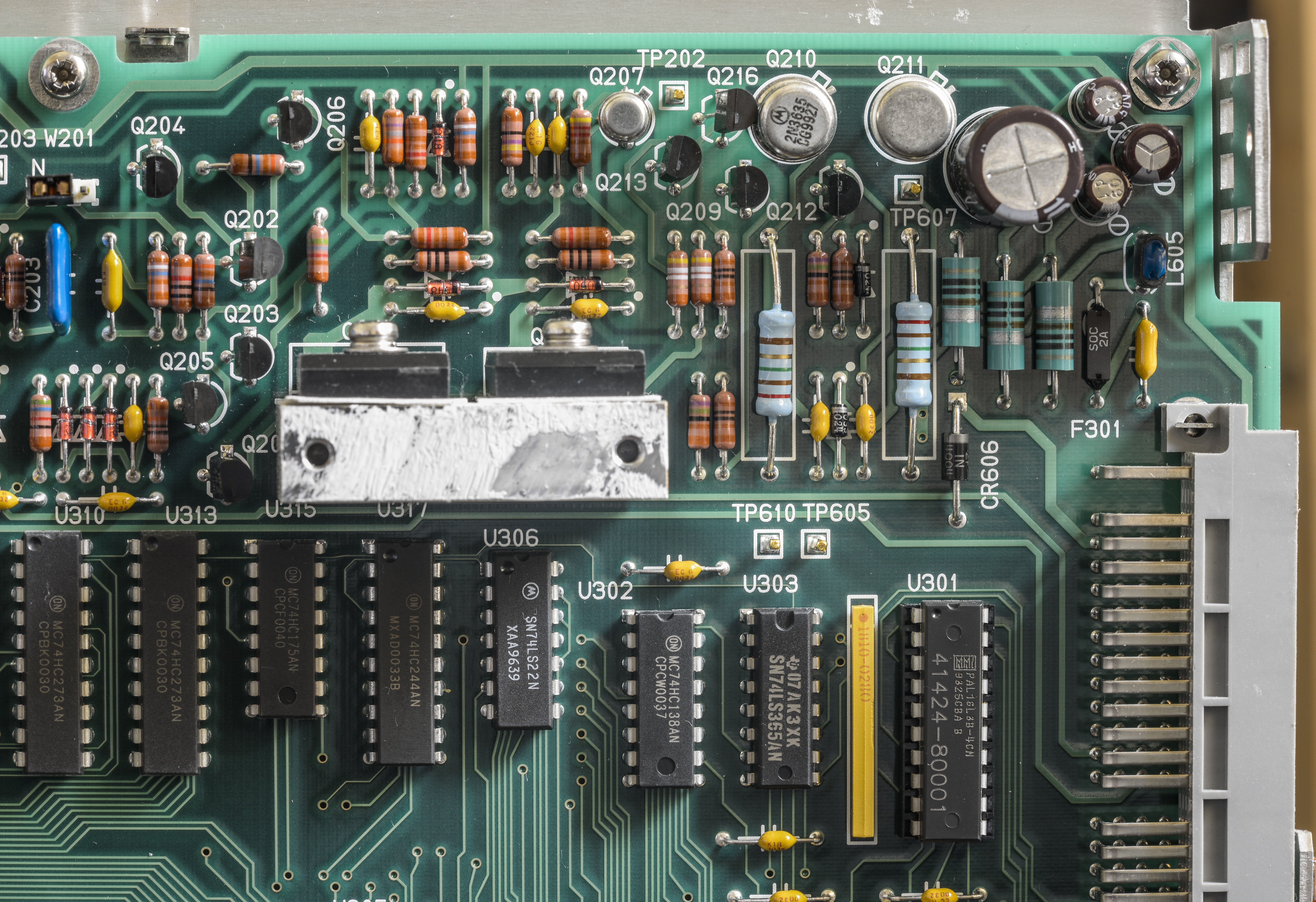
Now let’s remove some crews and look inside this versatile SMU module.

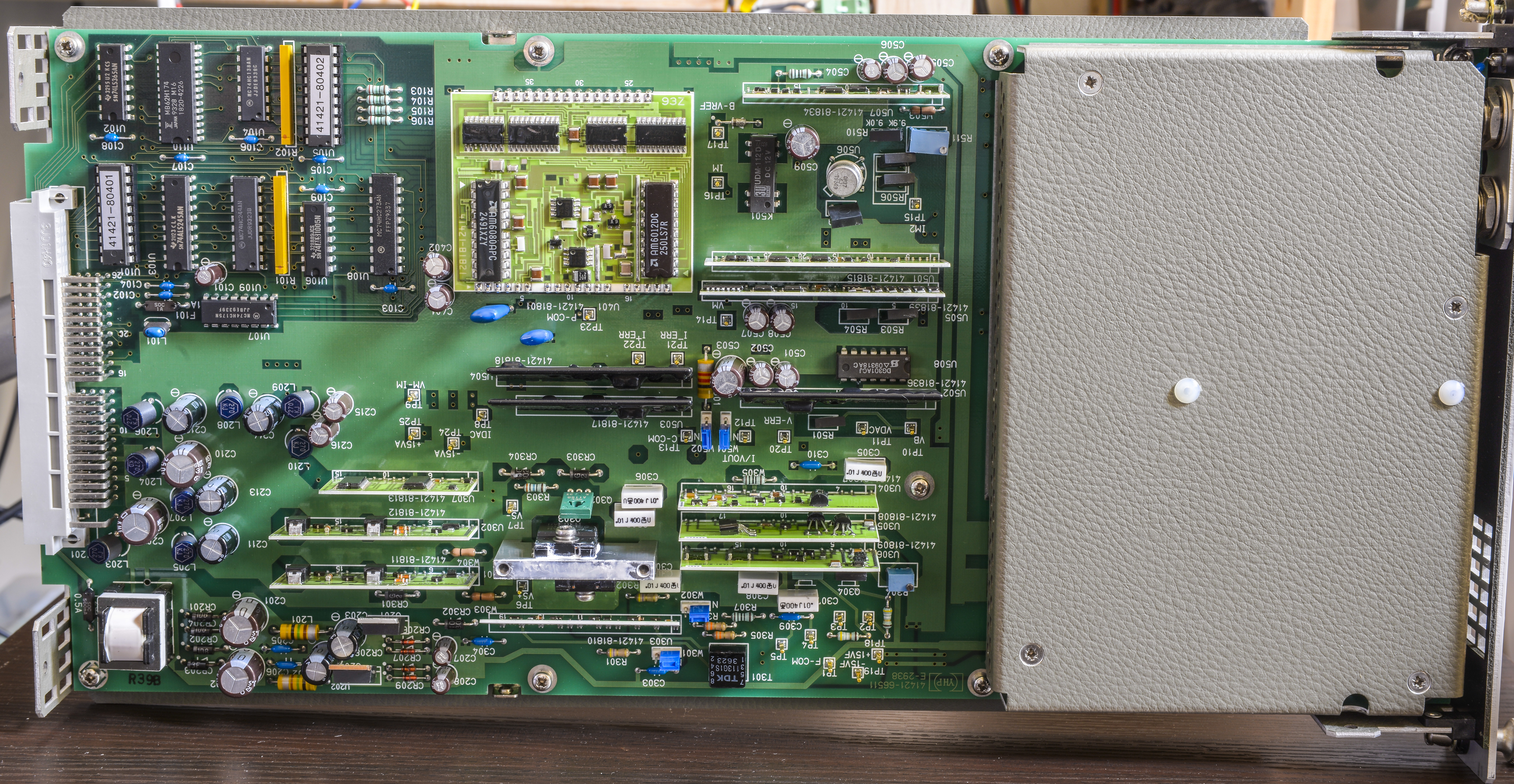
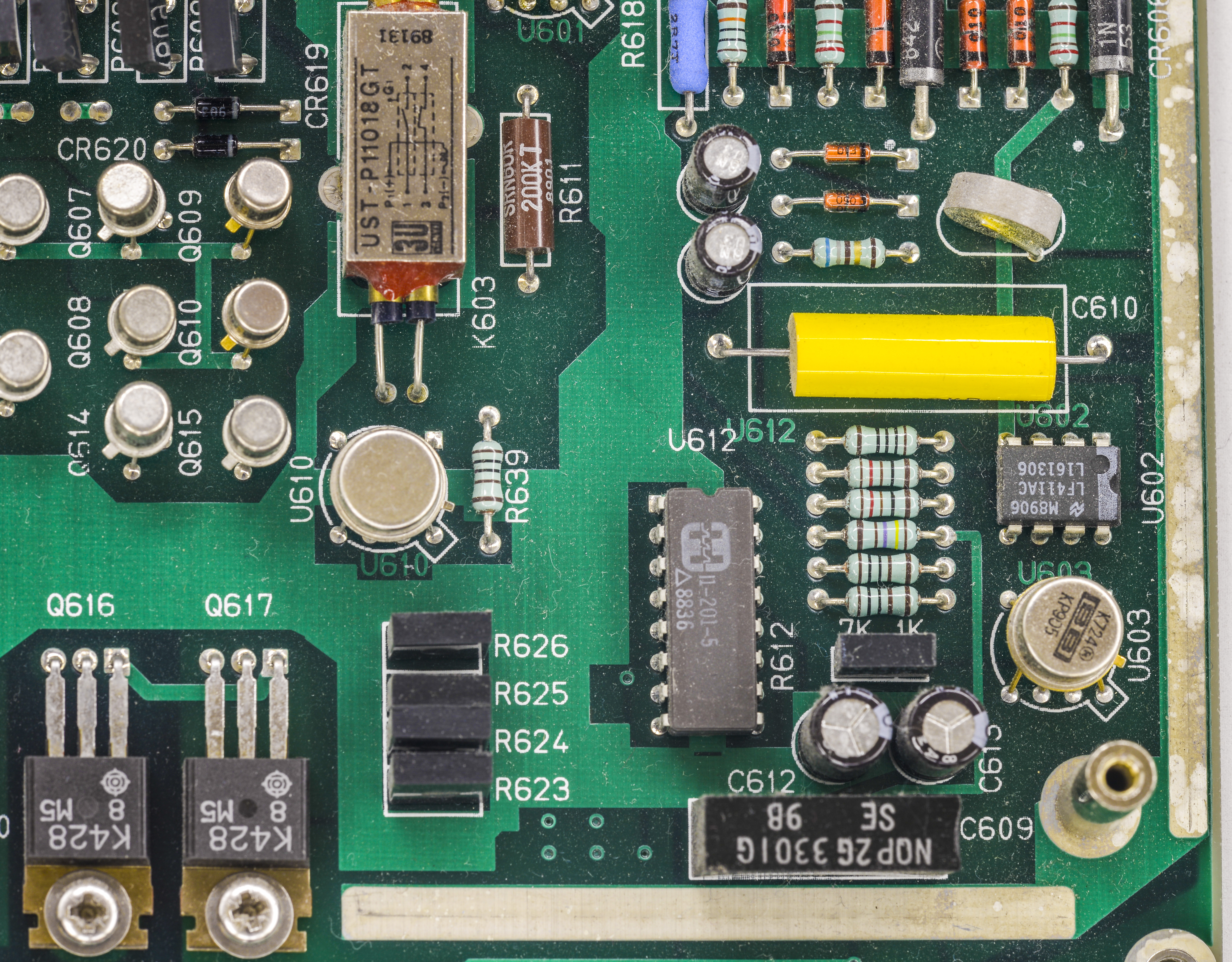
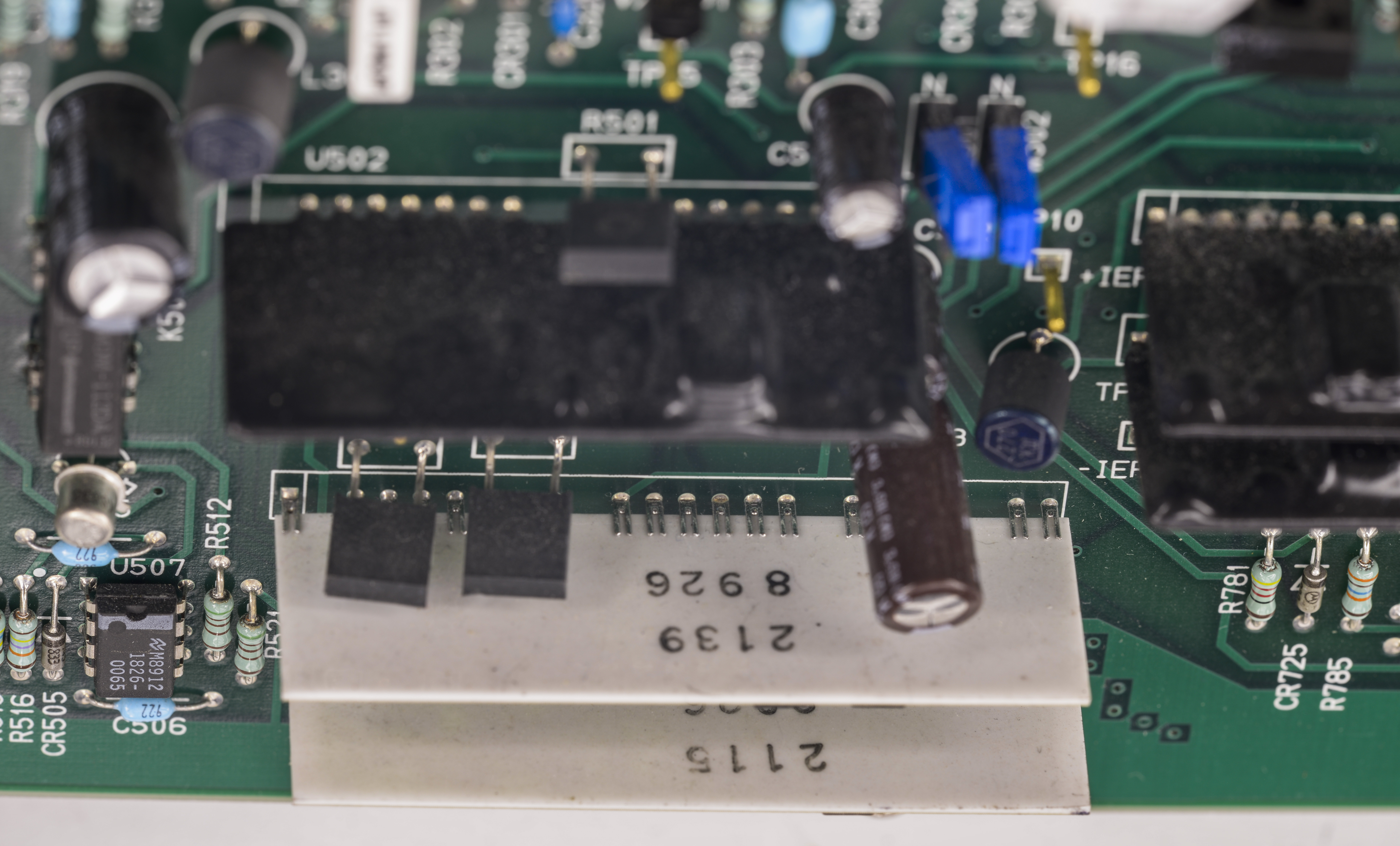
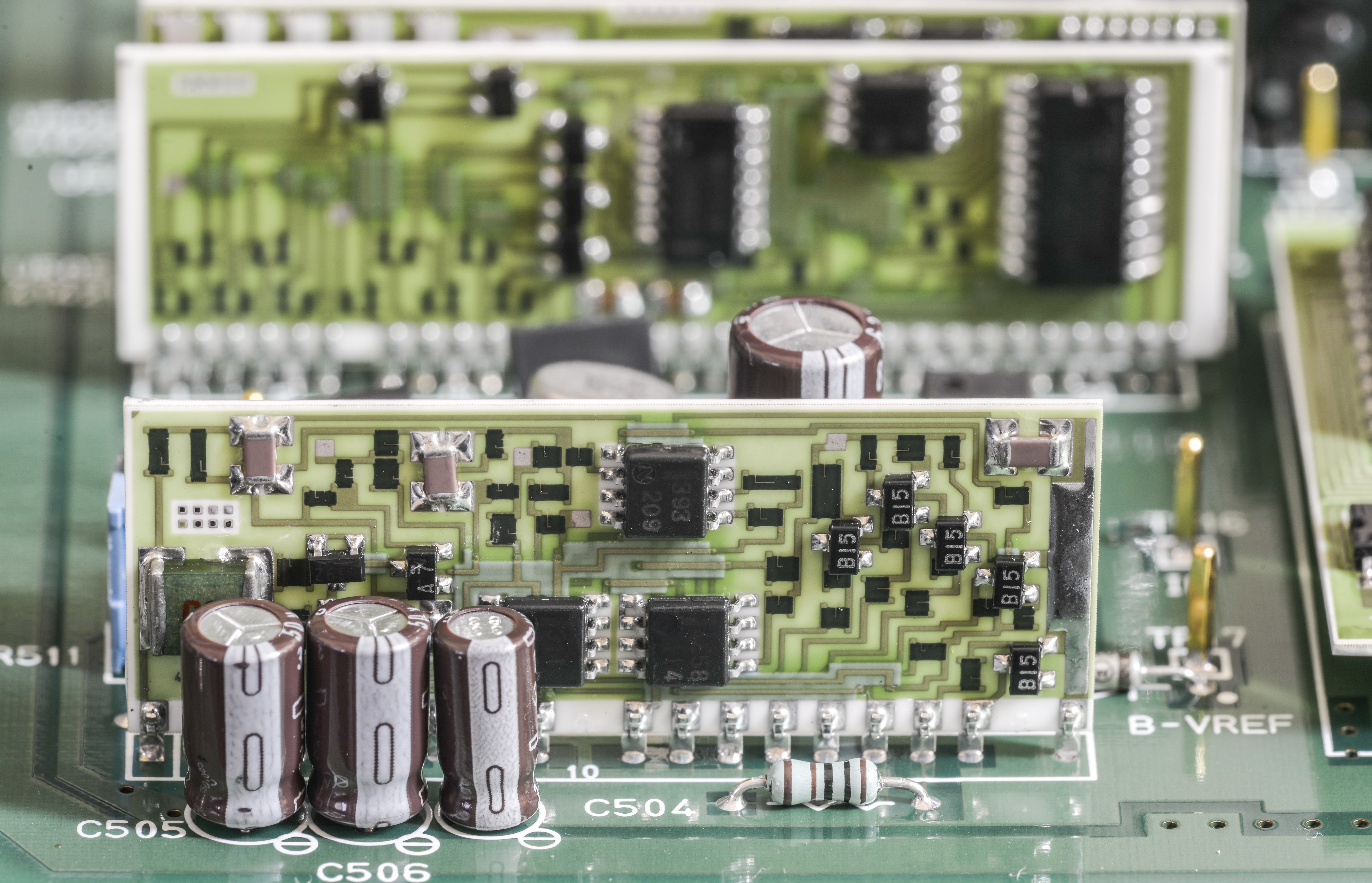
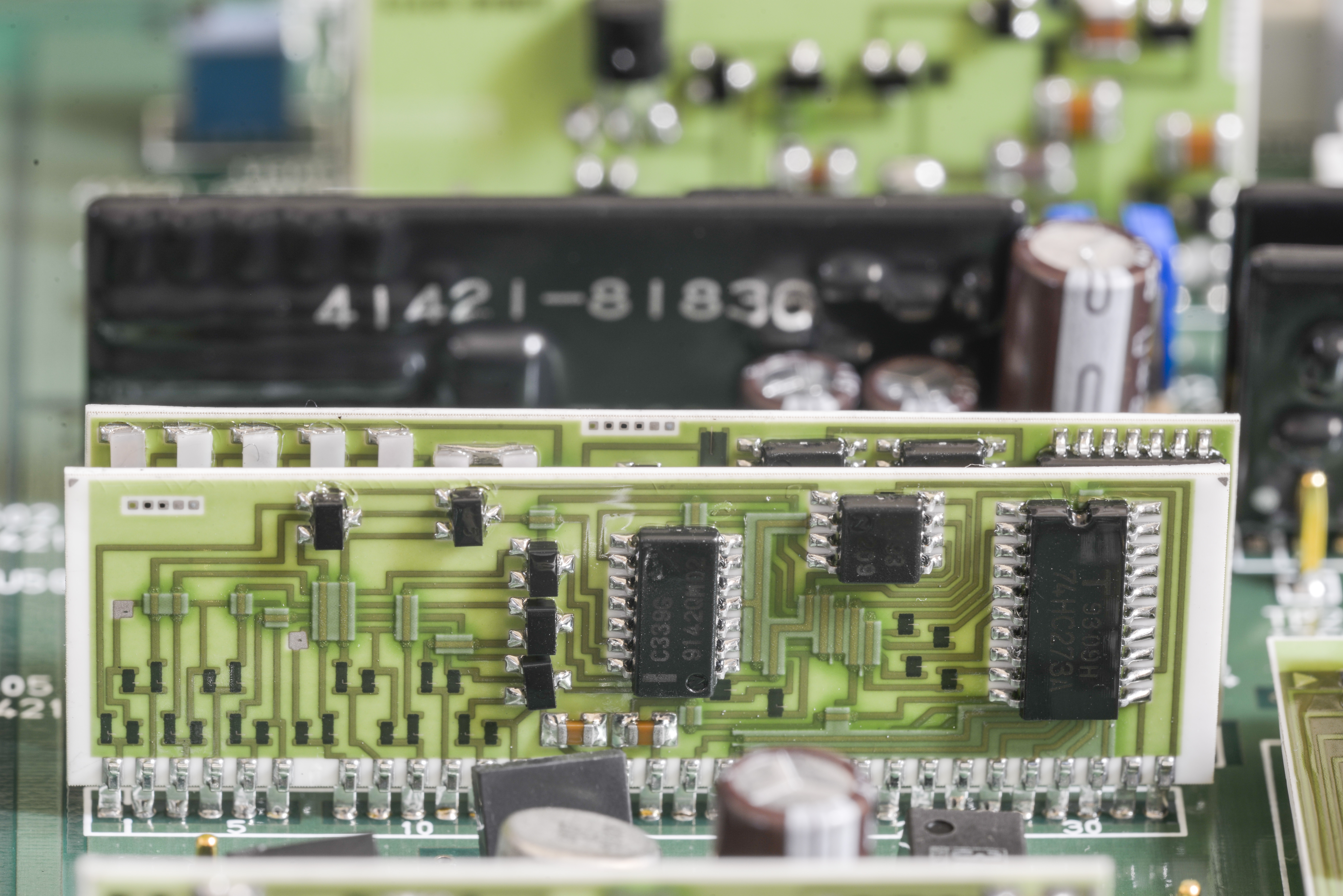
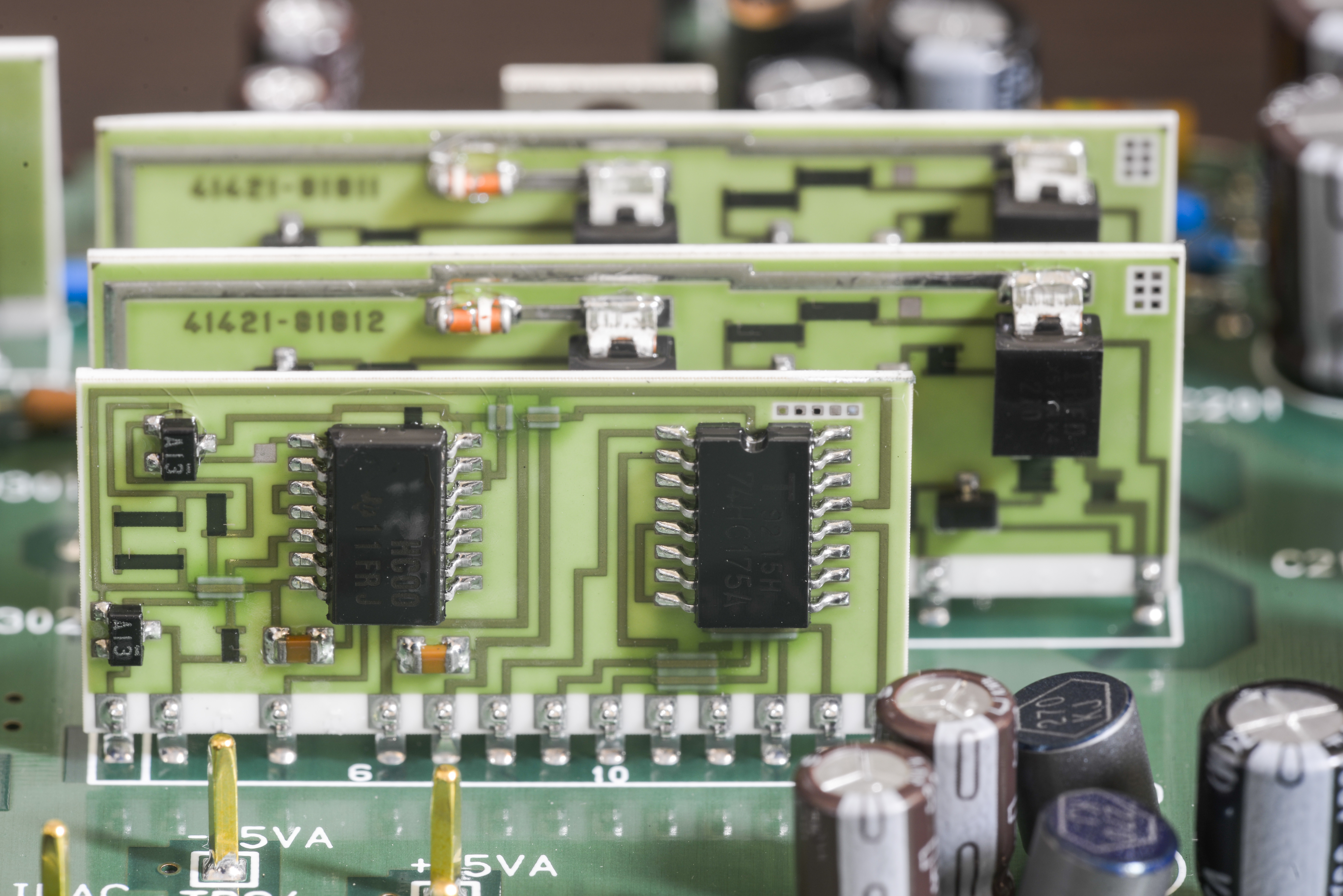
Right away we are greeted by no less than 14 hybrid circuits on ceramic substrate.

PCB is marked with YHP 41421-66511 label, with parts date codes from 1992. Some of test points clearly marked as I/VOUT, VDAC and such.

Most of hybrids are vertical standing, but one large parallel to main PCB is soldered down with metal pins.
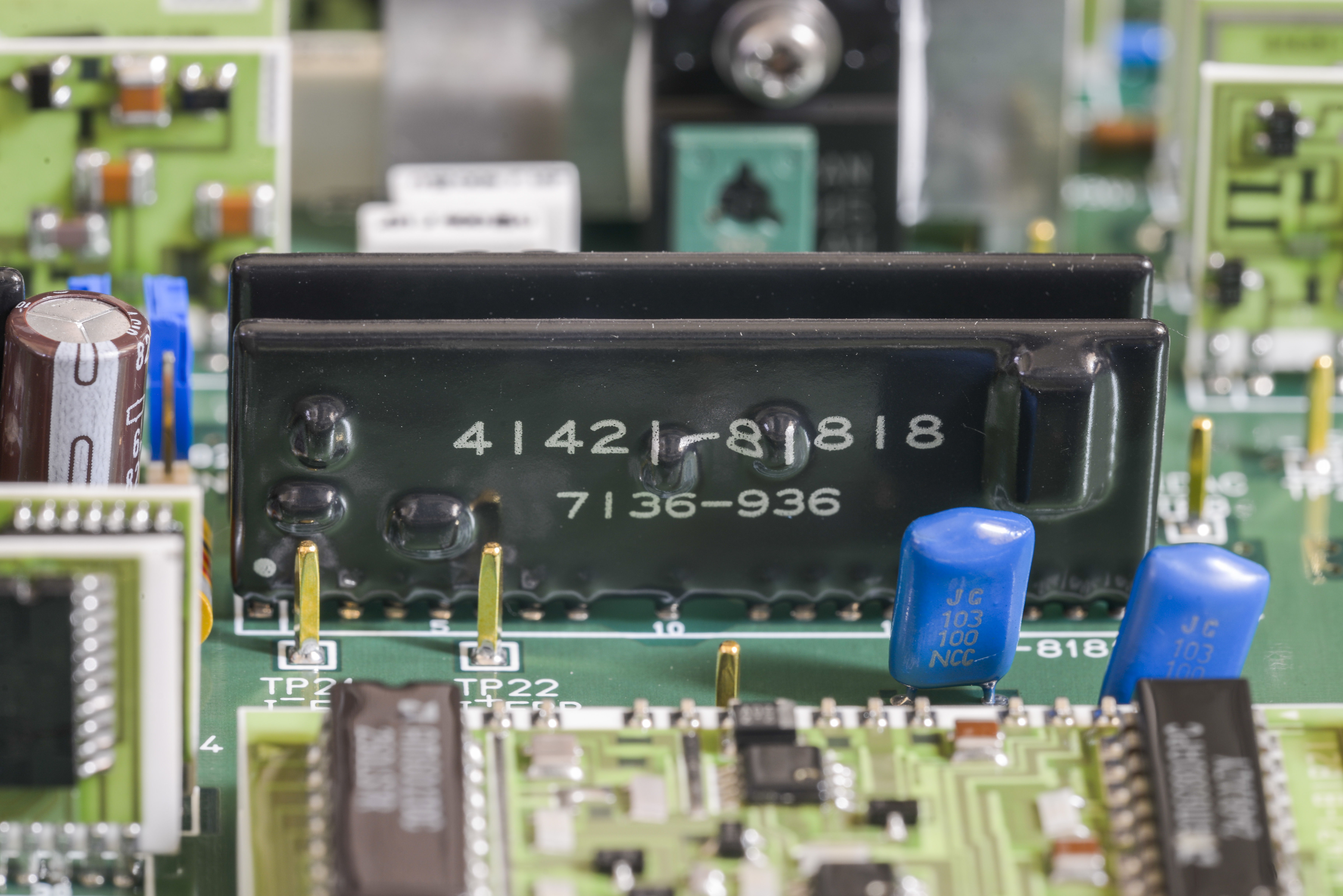
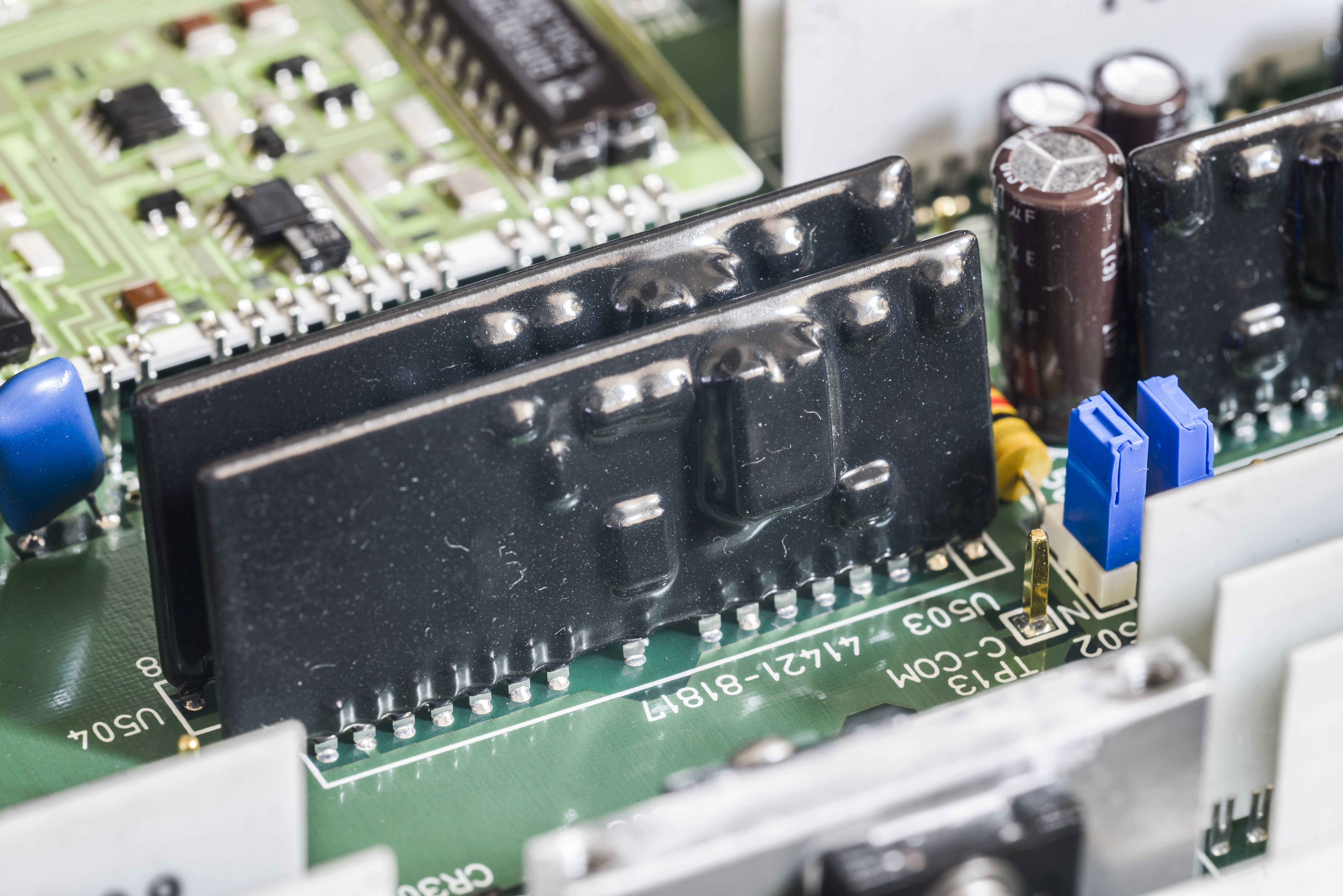
This module features pair of DACs, AM6080APC (8-bit DAC) and AM6012DC (12-bit DAC) and few packages of control logic 74HC175 and 74HC273.
Three of modules are in hard black epoxy, while others just have clear protective coating.
Analog power of SMU have own input transformer, rectifier and 7815CT in TO-220 package. There is logic interface with few PALs as well.
Few NEC transistors have green plastic package, which is not very usual :).


More green transistors:
All hybrids are unique, they do not match each other.
Most of the routing on ceramic substrate is done in single layer, but some of the bridges are on second layer over lighter insulation layer. So essentially it is dual-layer design.
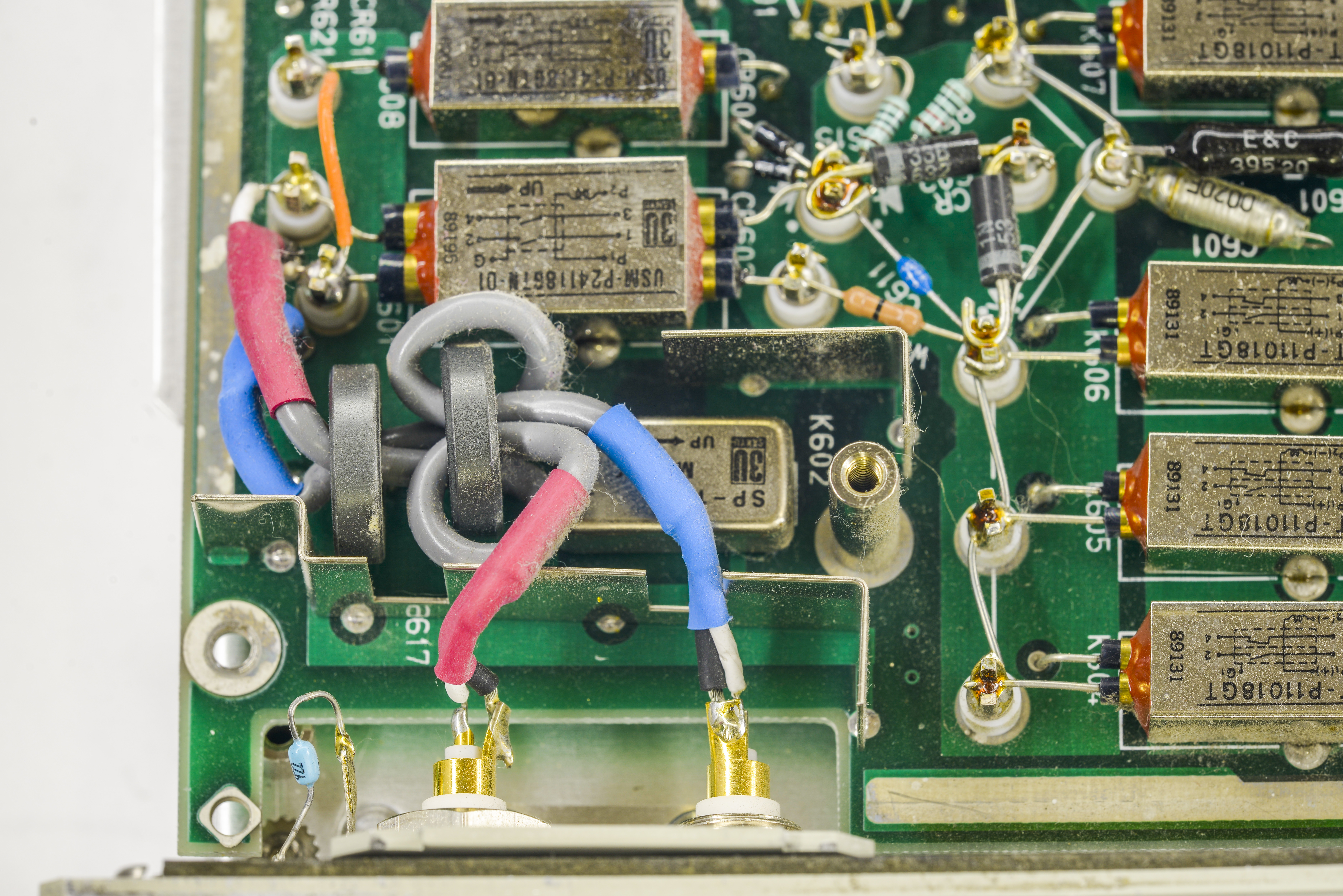
High-impedance section is shielded by separate inner aluminum cover, likely actively guarded just like triaxial connector guard shell. This is a must to ensure performance of the unit on lowest 1nA range.


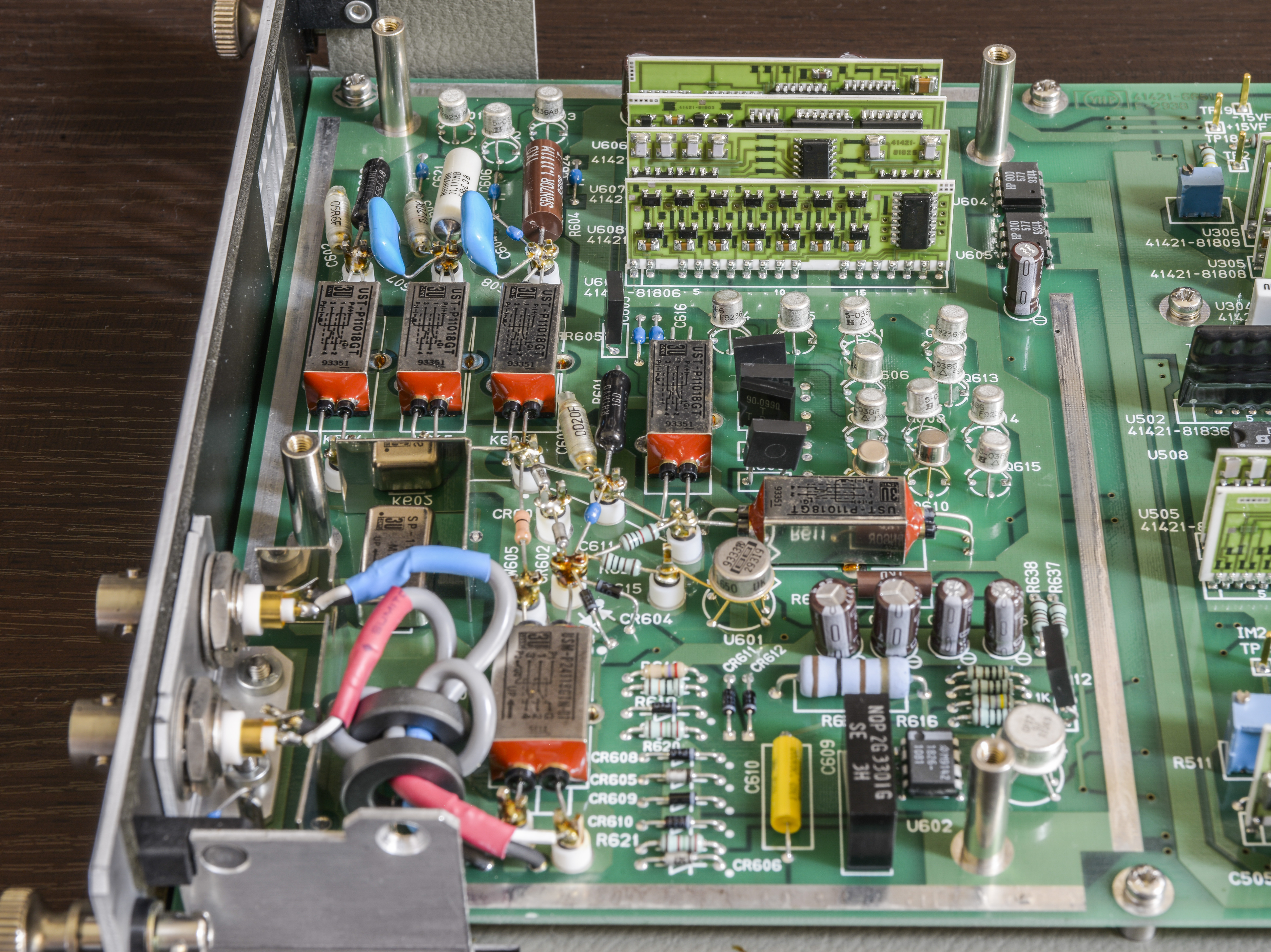
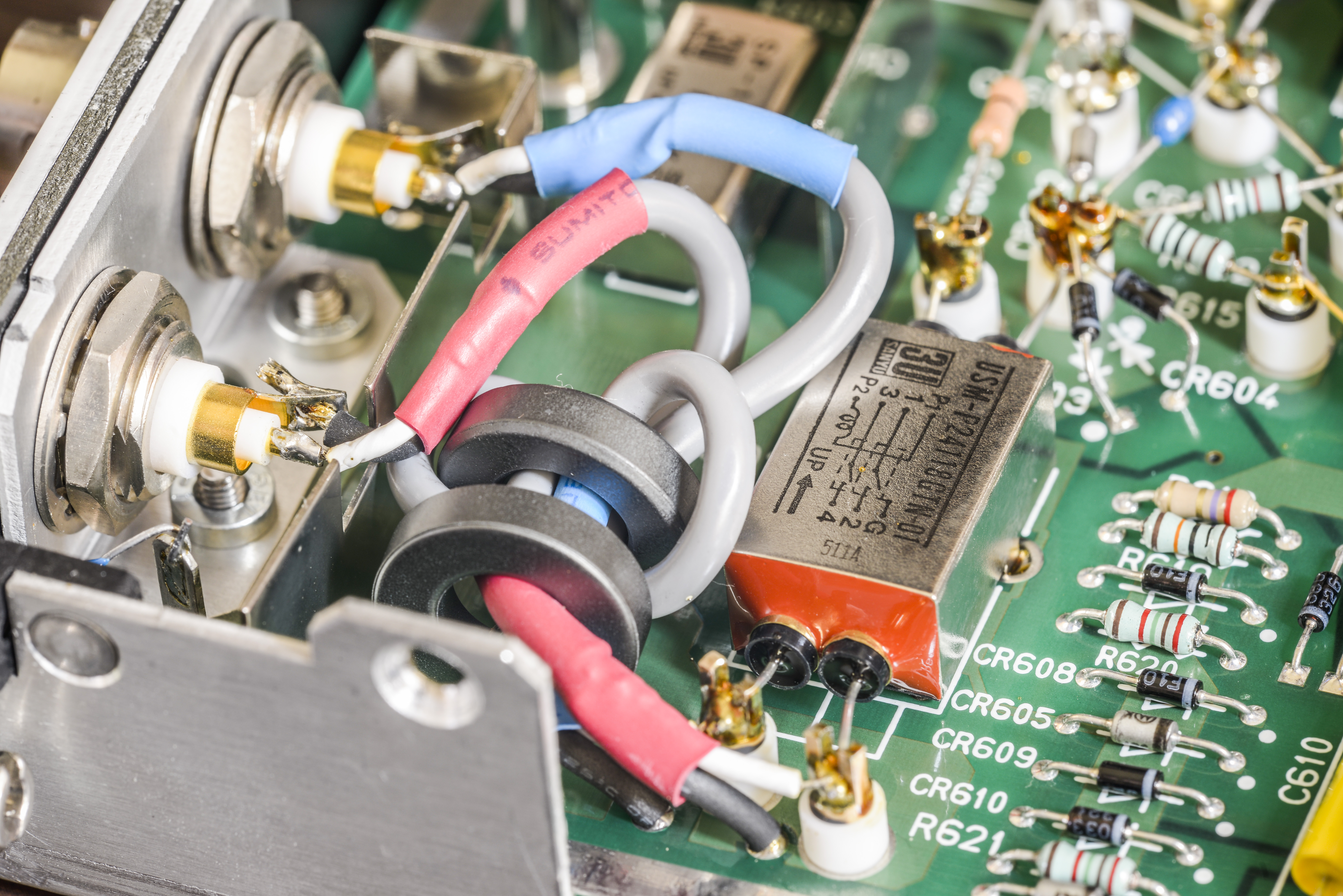
Triaxial wiring inside the module:
This part of board also have few hybrids:

There are some opamps, mostly OP-series and AE foil resistors.

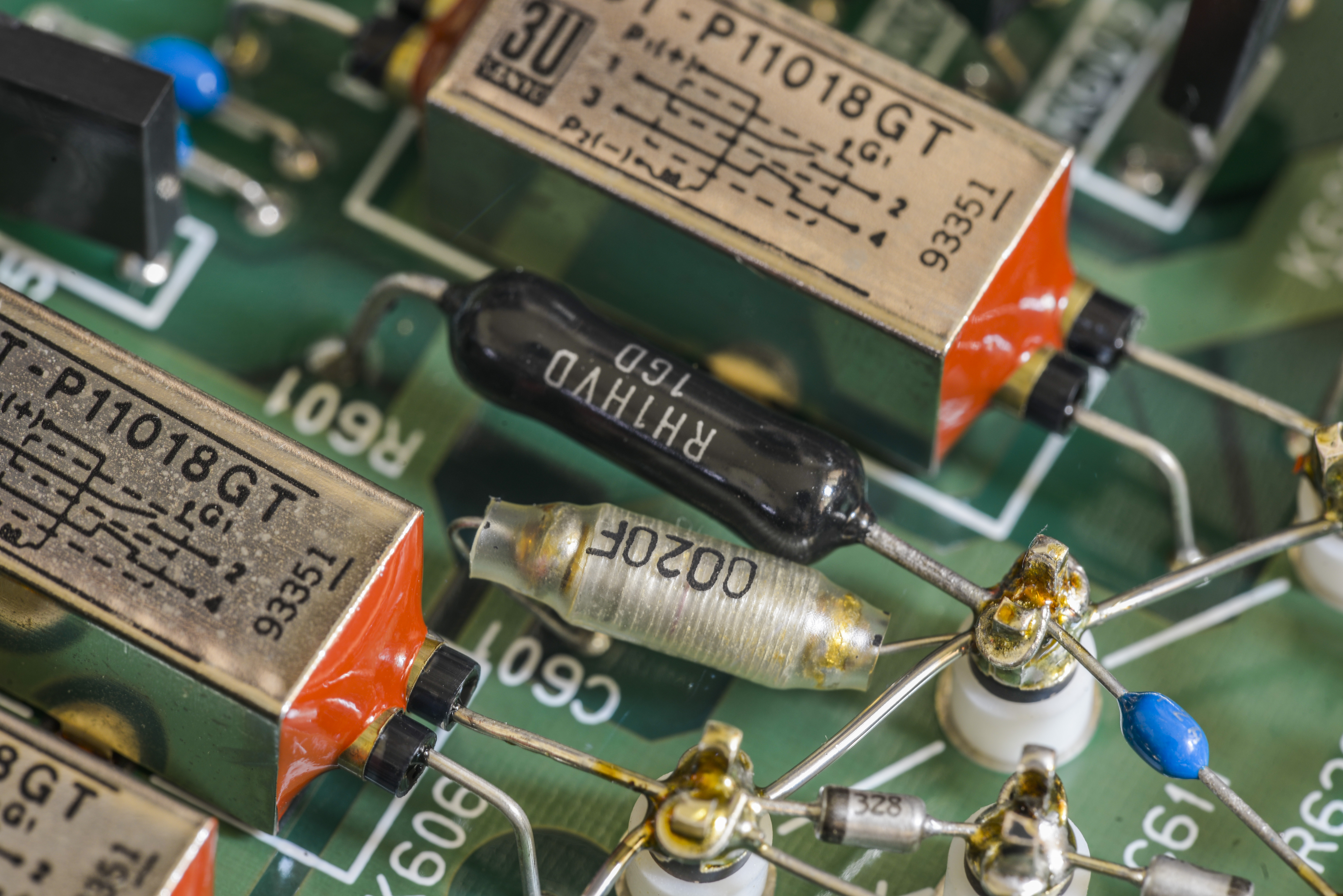
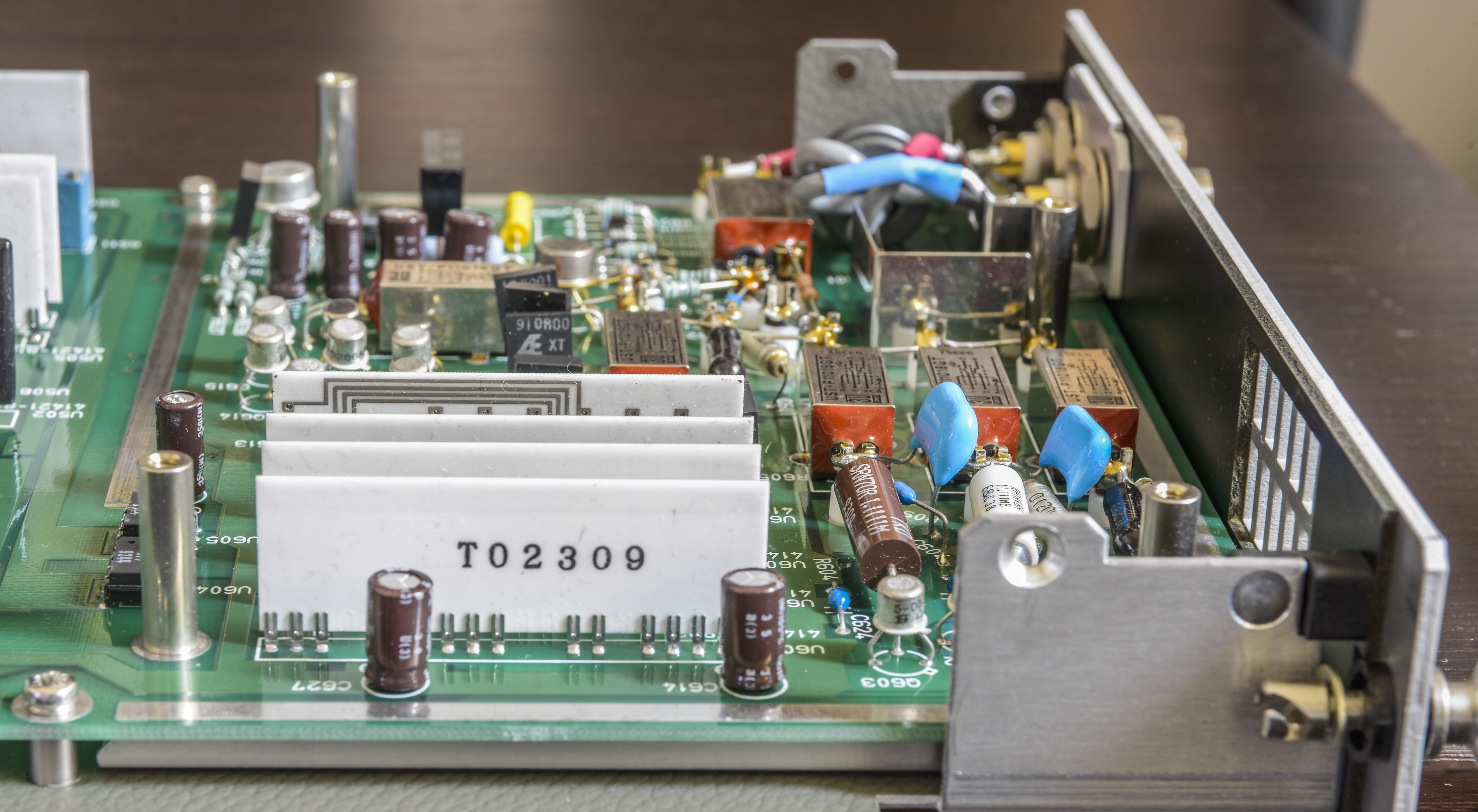
High value resistors and shielded dual-contact reed UST series relays made by 3U Relays are installed on teflon standoffs to ensure lowest leakage possible. With such low currents usual PCB surface is not good enough anymore. This is common design approach for low-current applications, usually found on electrometers and SMU frontends.
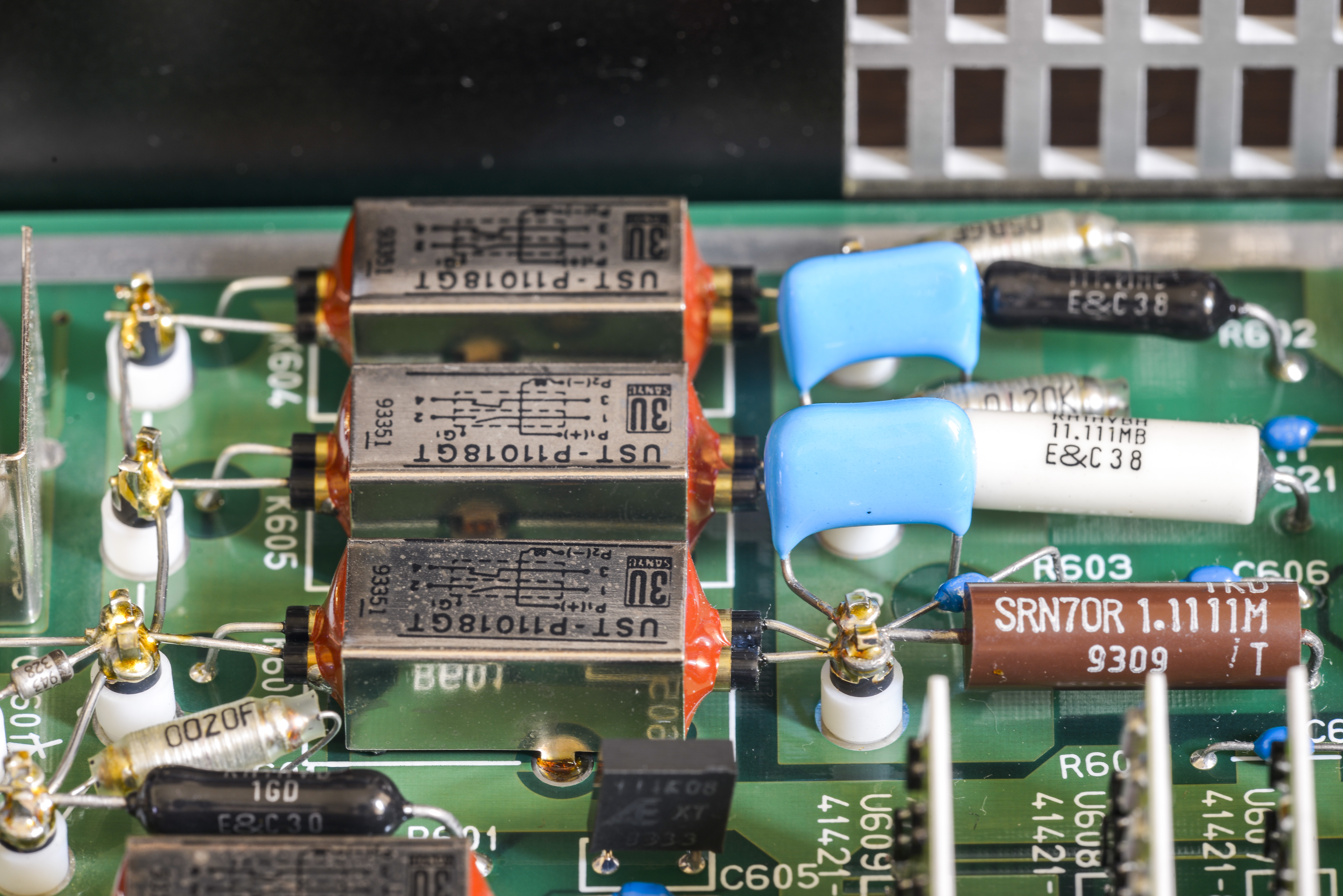

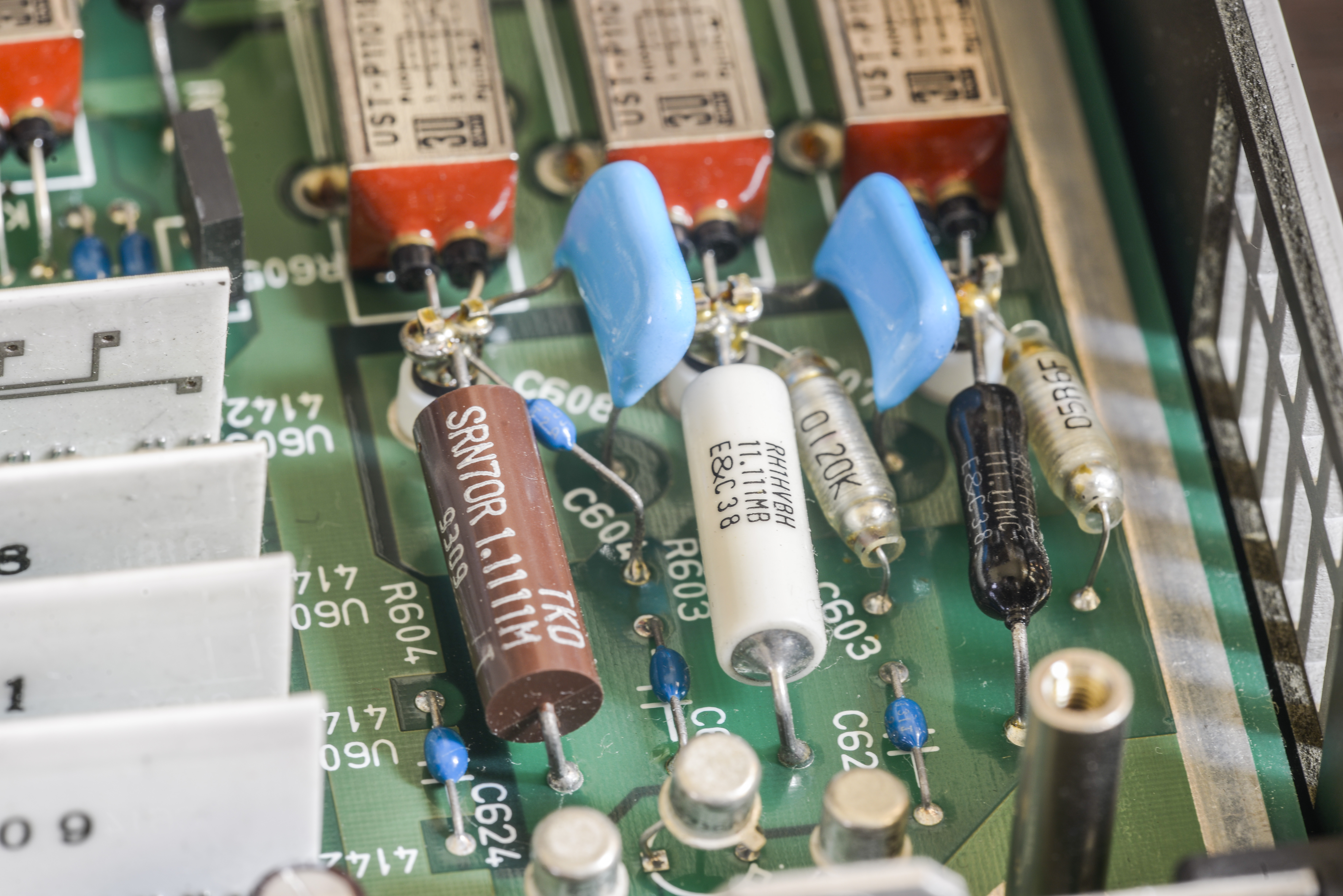
More close-ups on low-leakage design parts:

Area around triaxial ports is further shielded by metal sheets.
There are some AE foil resistors around and pair of resistor networks in same package.

Teflon standoffs used extensively on main source/measure front-end signal path.
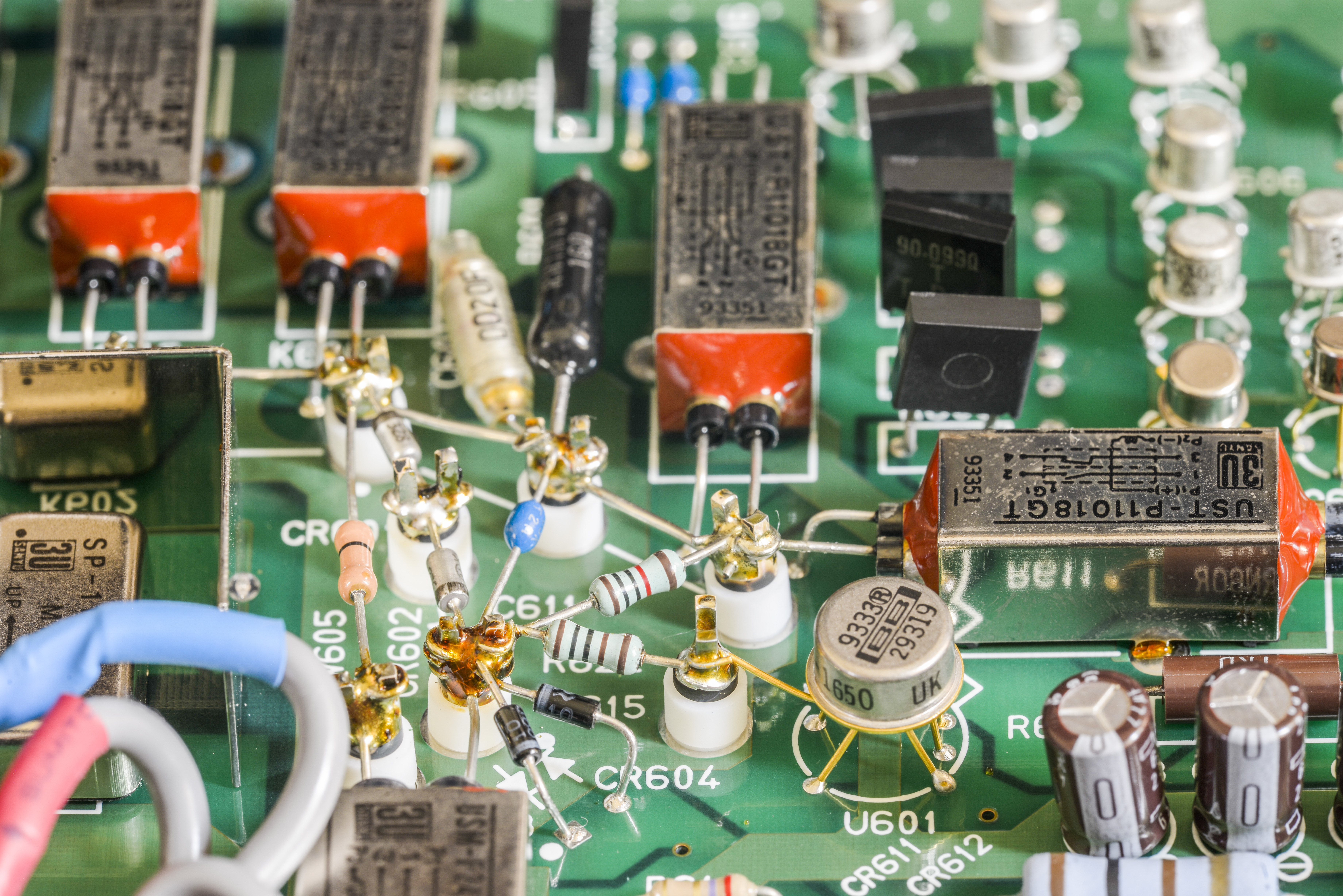
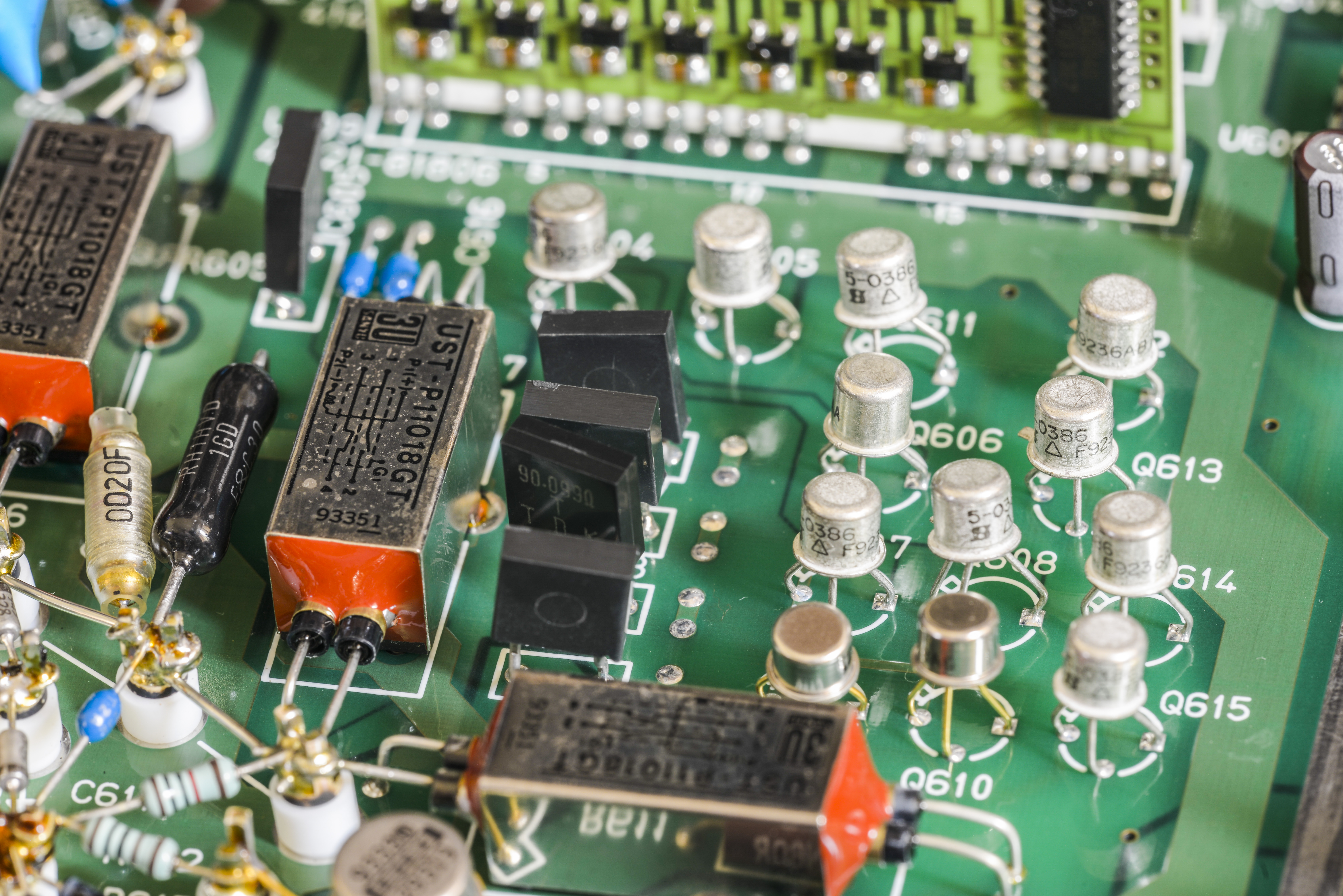
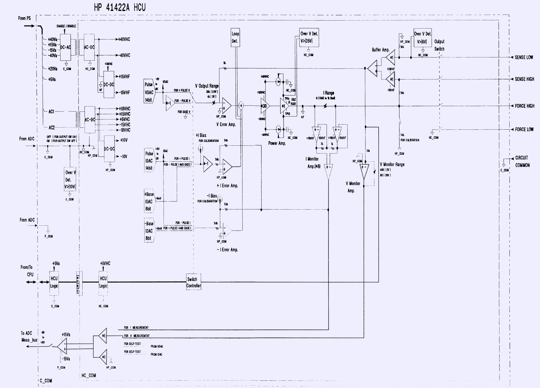
HP 41422A HCU High-current Source/Monitor 10V/10A Unit
This module takes 2 slots in 4142B. I don’t have this module (yet?), so only specs provided here for reference.
| Function | Output | Set Resolution | Max load | Accuracy |
|---|---|---|---|---|
| Voltage source/measure | -2.0000 … 2.0000 V | 200 µVDC | 10 A | ±0.5% + 10mV |
| Voltage source/measure | -20.000 … 20.000 V | 20 mVDC | 10 A | ±0.5% + 100mV |
| Current source/measure | -1.0000 … 1.0000 mA | 20 nA | ±10V | ±0.5% + 2µA + 100nA × VOUT |
| Current source/measure | -10.000 … 10.000 mA | 200 nA | ±10V | ±0.5% + 20µA + 1µA × VOUT |
| Current source/measure | -100.00 … 100.00 mA | 2 µA | ±10V | ±0.5% + 200µA + 10µA × VOUT |
| Current source/measure | -1.0000 … 1.0000 A | 20 µA | ±10V | ±1% + 2mA + 100µA × VOUT |
| Current source/measure | -10.000 … 10.000 A | 200 µA | ±10V | ±2% + 20mA + 1mA × VOUT |
Block diagram:
HP 41423A HVU High-voltage Source/Monitor 1000V/10mA Unit
This module takes 2 slots in 4142B. I don’t have this module (yet?), so only specs provided here for reference.
| Function | Output | Set Resolution | Max load | Accuracy |
|---|---|---|---|---|
| Voltage source/measure | -100.00 … 100.00 V | 10 mVDC | 10 mA | ±0.5% + 0.5V |
| Voltage source/measure | -200.00 … 200.00 V | 20 mVDC | 10 mA | ±0.5% + 1V |
| Voltage source/measure | -500.00 … 500.00 V | 50 mVDC | 10 mA | ±0.5% + 2.5V |
| Voltage source/measure | -1000.0 … 1000.0 V | 100 mVDC | 10 mA | ±0.5% + 5V |
| Current source/measure | -100.00 … 100.00 nA | 50 pA | ±1000V | ±1% + 1nA |
| Current source/measure | -1.0000 … 1.0000 µA | 500 pA | ±1000V | ±1% + 10 nA |
| Current source/measure | -10.000 … 10.000 µA | 5 nA | ±1000V | ±1% + 100 nA |
| Current source/measure | -100.00 … 100.00 µA | 50nA | ±1000V | ±1% + 1 µA |
| Current source/measure | -1.0000 … 1.0000 mA | 500 nA | ±1000V | ±1% + 10 µA |
| Current source/measure | -10.000 … 10.000 mA | 5 µA | ±1000V | ±1% + 100 µA |
Block diagram:
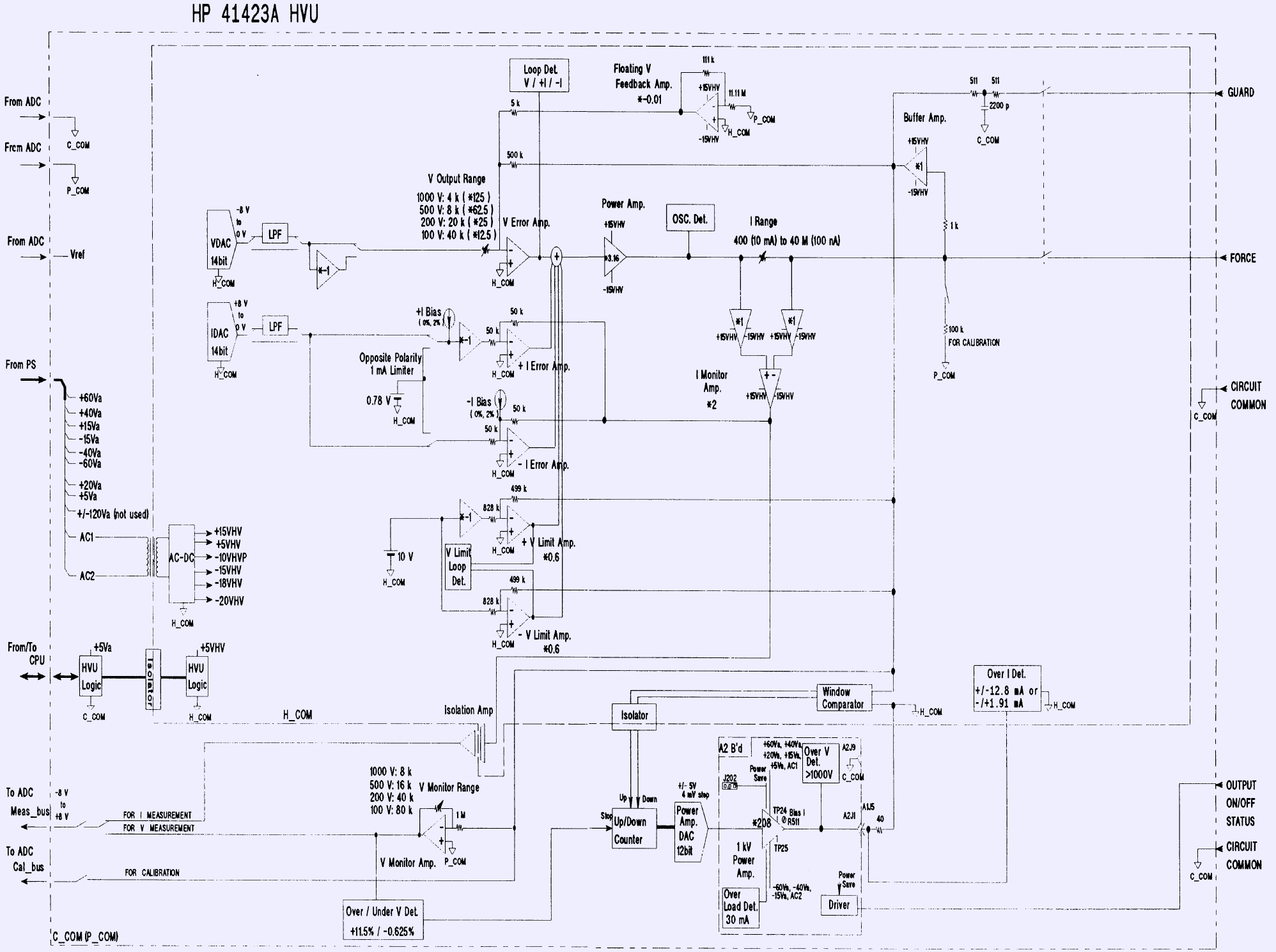
Photo of the board from Keysight Find-A-Part section:
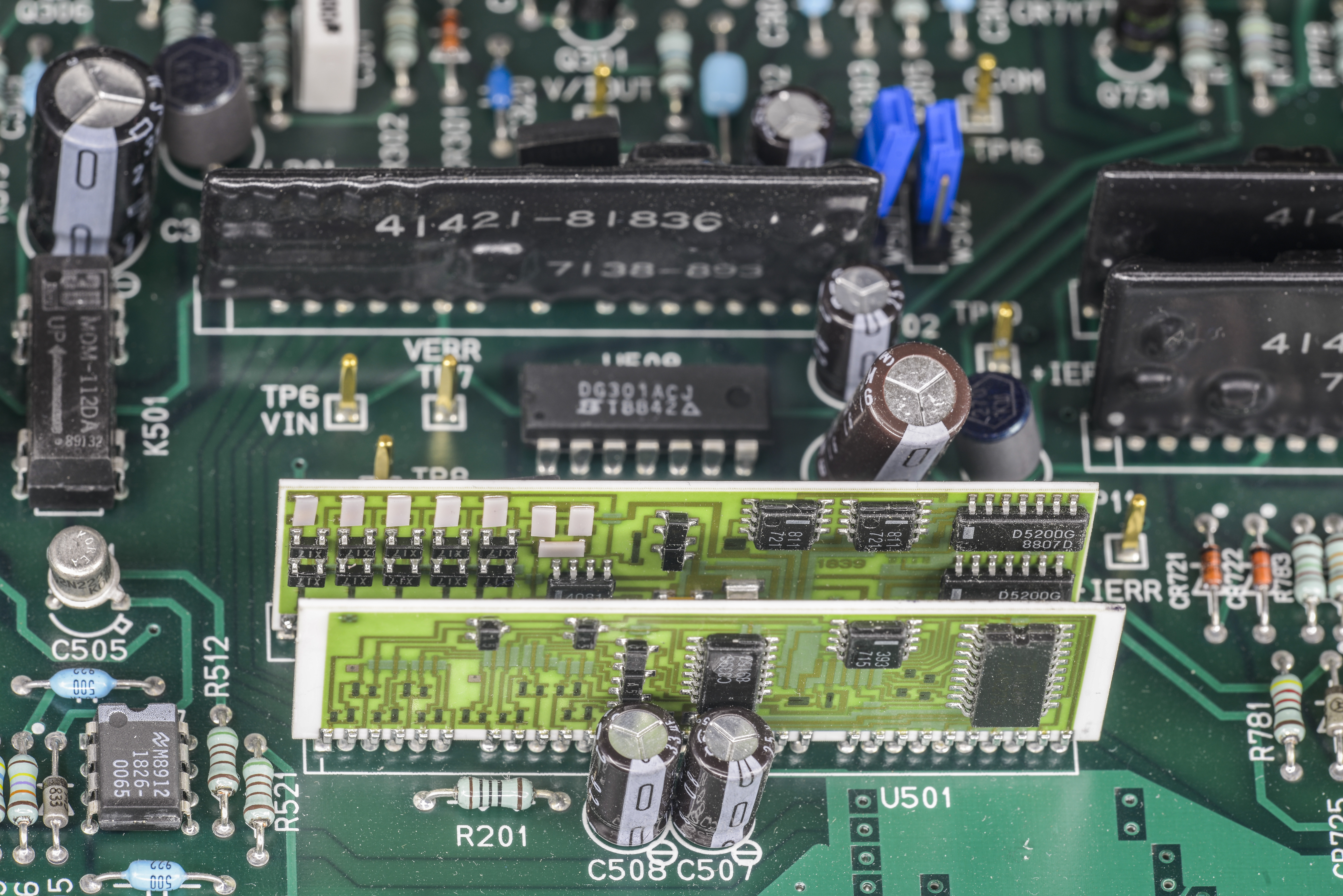
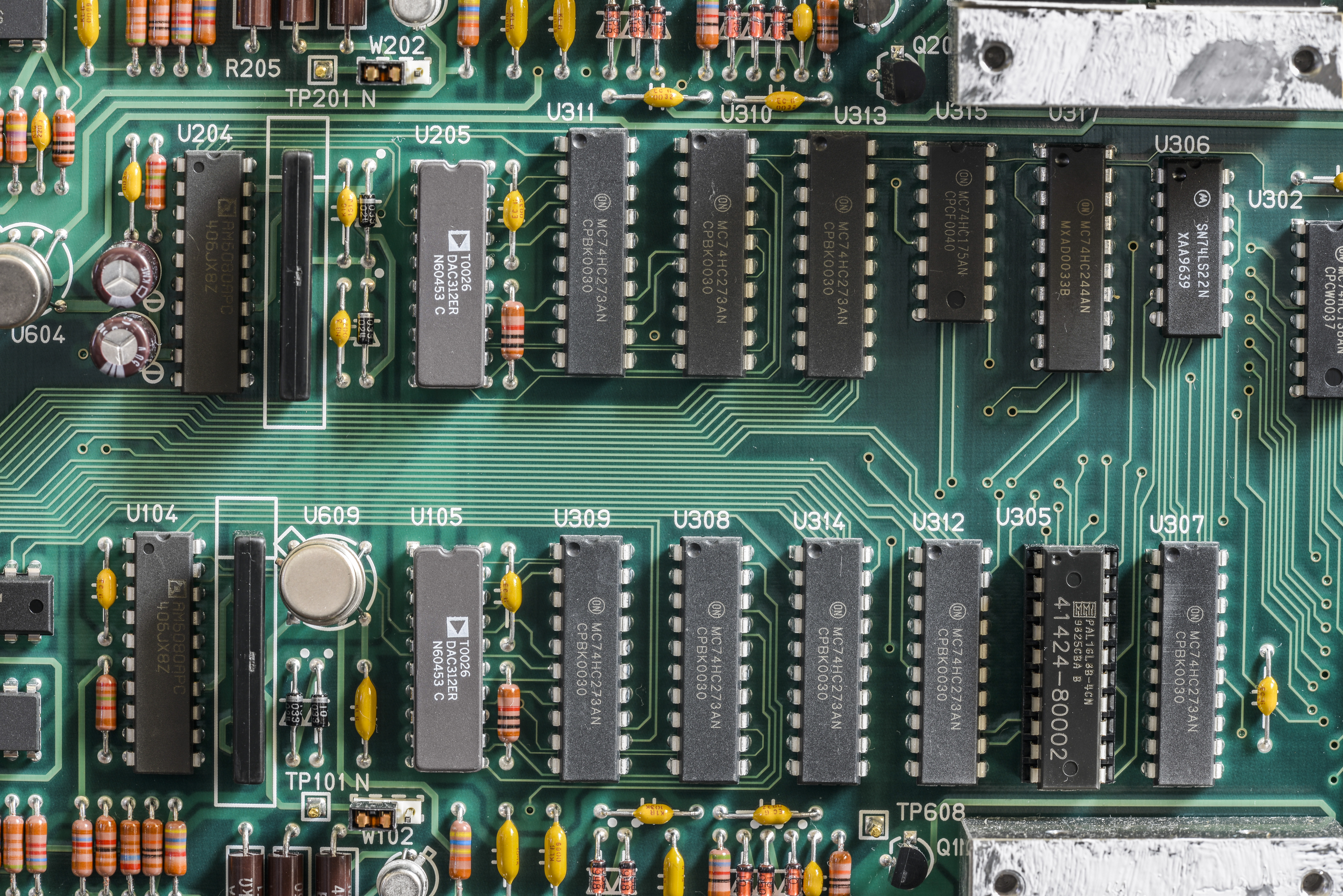
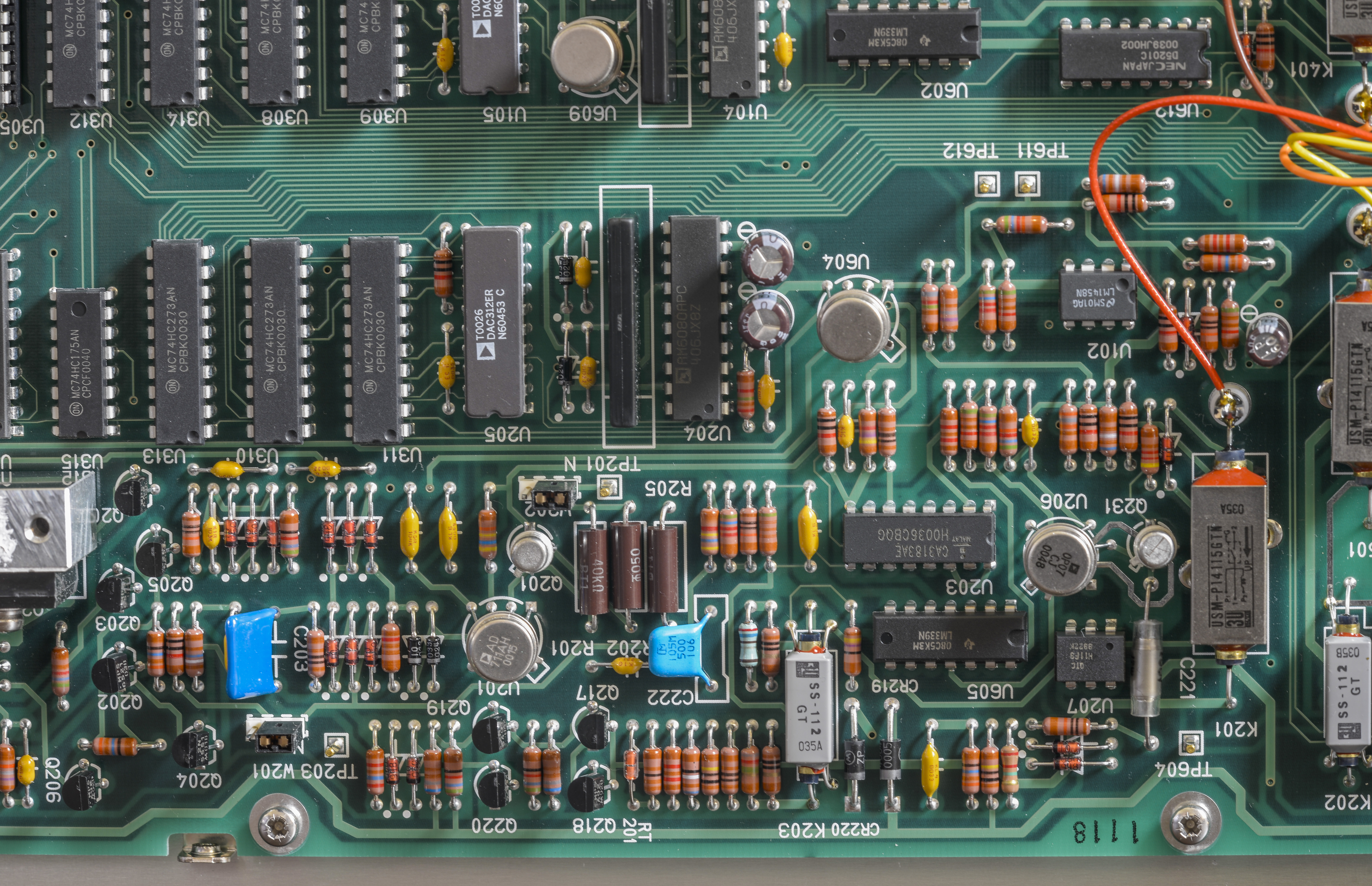
HP 41424A V source/V Monitor Unit
I have two of the same VS/VM modules, they are exactly same, so no point to focus on each one photos specifically.
| Function | Output | Resolution | Max load | I-monitor | Resolution |
|---|---|---|---|---|---|
| Voltage source (each ch) | 0…20.000 V | 1 mVDC | 100 mA | 0…100.0mA | 100 µA |
| Voltage source (each ch) | 0…40.000 V | 2 mVDC | 20 mA | 0…20.00mA | 20 µA |
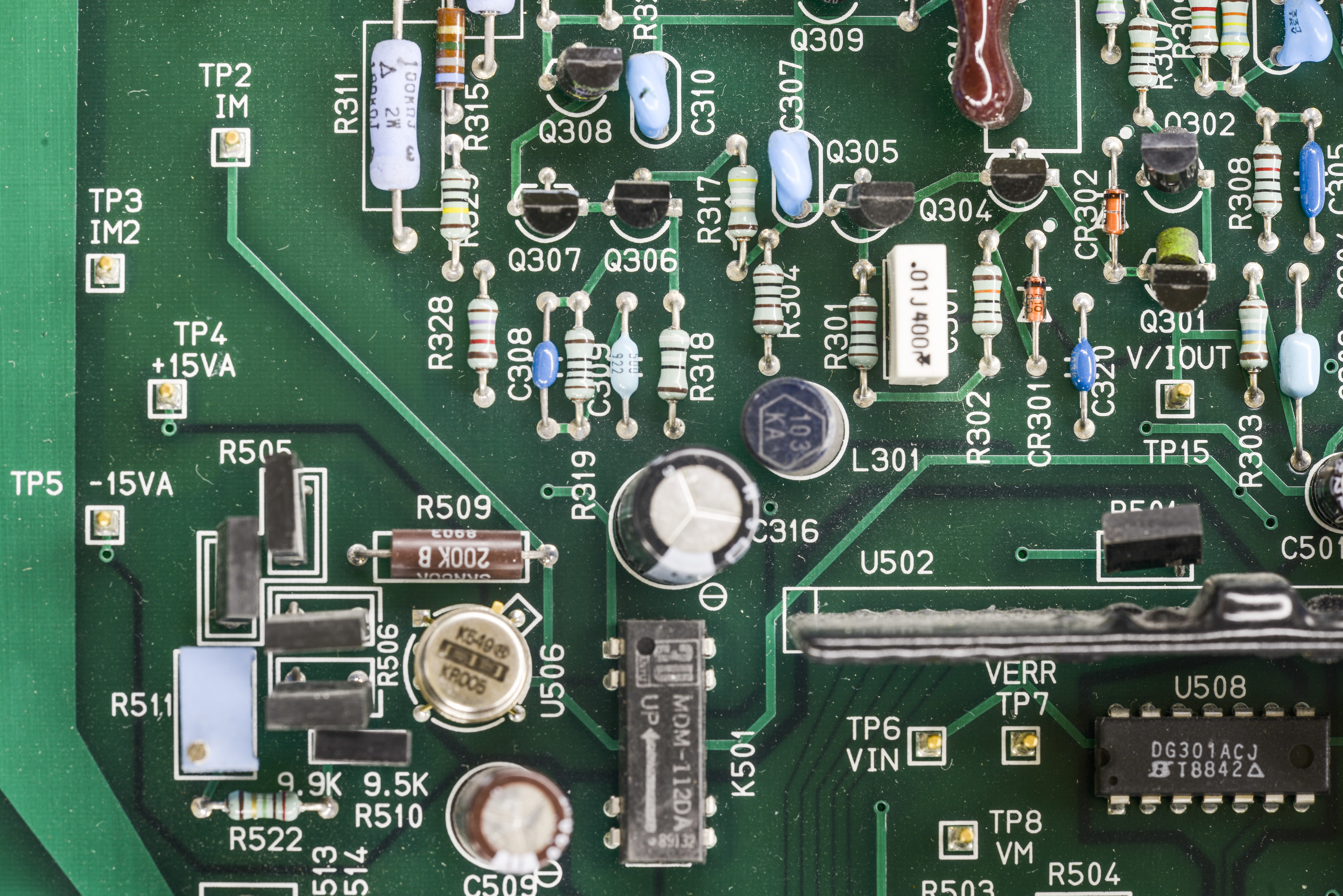
This module have two independent voltage sources (VS1 and VS2) and two voltage monitors (VM1 and VM2) which can be used for single-ended or differential measurement. All sources and monitors are referenced to GNDU measurement ground level. It takes single slot in mainframe.

Both channels are functionally equivalent and using same parts in front end. Main DAC is Analog Devices DAC312ER. This is high-speed multiplying DAC with 12-bit of resolution available. DAC non-linearity specified at 500ppm with settling time 250ns.
Outputs are current mode, 0 to 4 mA with internal voltage reference tempco ±10ppm/°C.
| Function | Input | Resolution | Max voltage |
|---|---|---|---|
| Voltage monitor (single-ended) | 0…2.30000 V | 40 µVDC | 40 VDC |
| Voltage monitor (single-ended) | 0…23.000 V | 400 µVDC | 40 VDC |
| Voltage monitor (single-ended) | 0…40.000 V | 800 µVDC | 40 VDC |
| Voltage monitor (diff VM1-VM2) | 0…0.230000 V | 4 µVDC | 40 VDC |
| Voltage monitor (diff VM1-VM2) | 0…2.30000 V | 40 µVDC | 40 VDC |
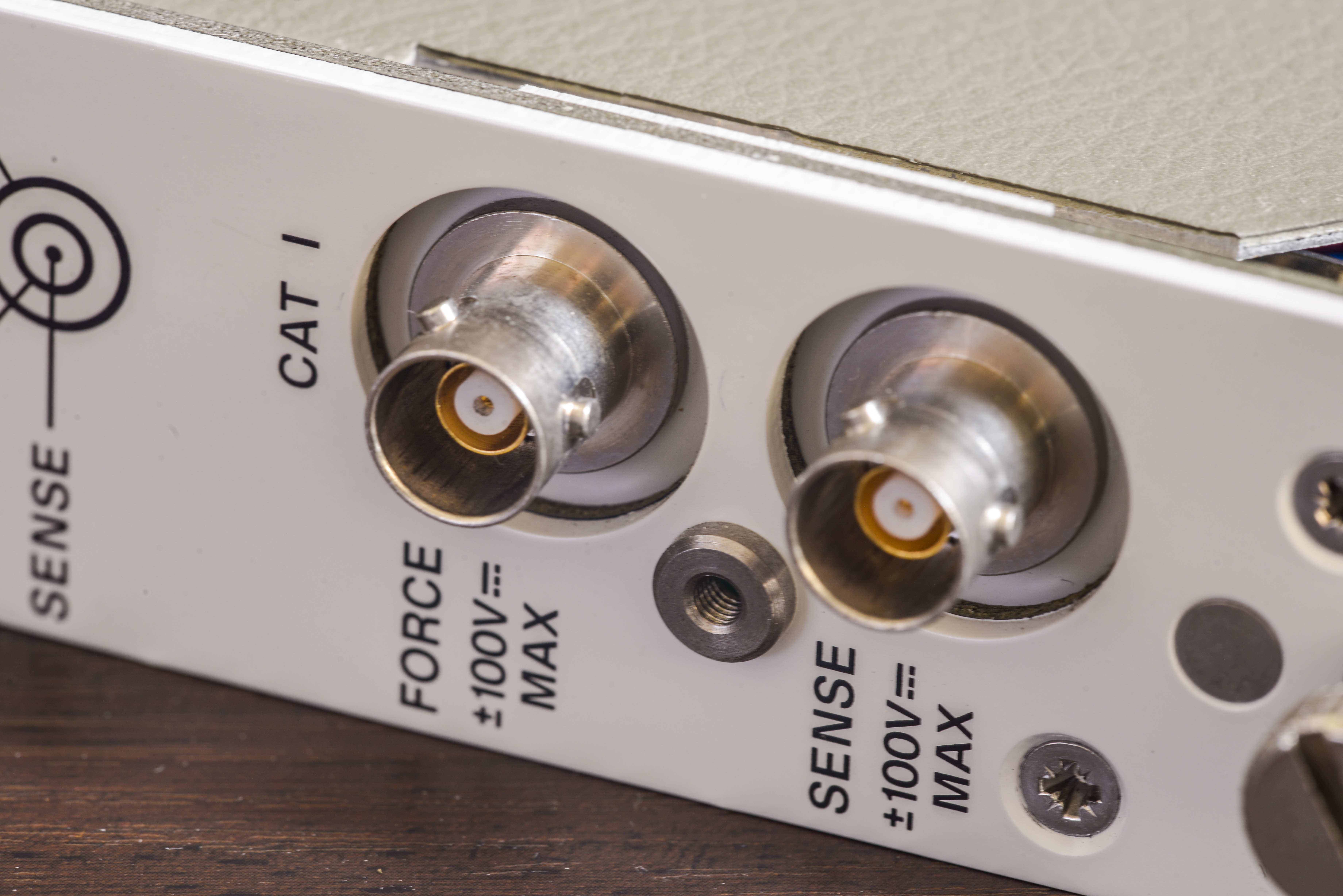
Module have regular BNC-type connectors, pair for ±40V voltage sources, and pair for ±40V voltage monitors.
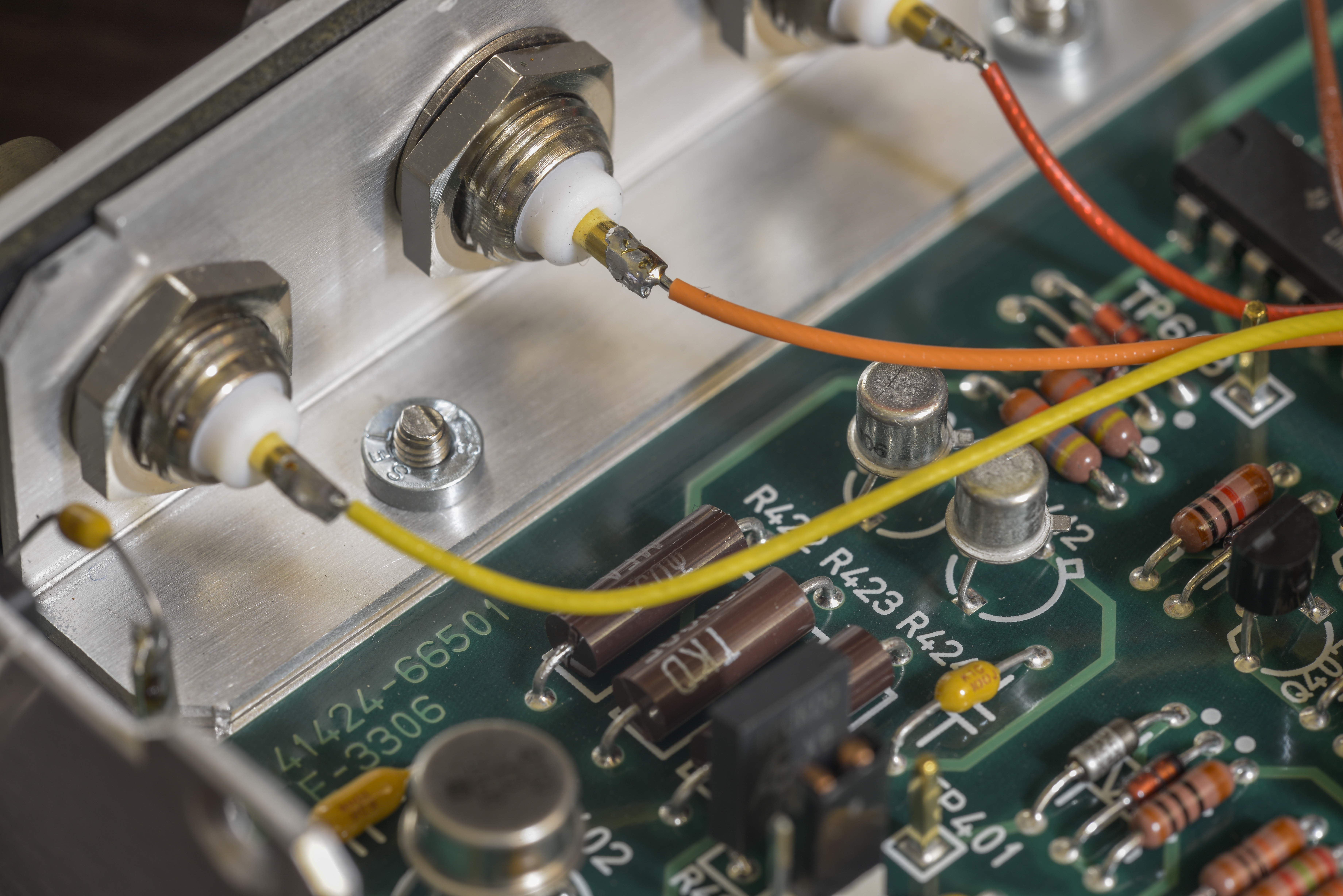
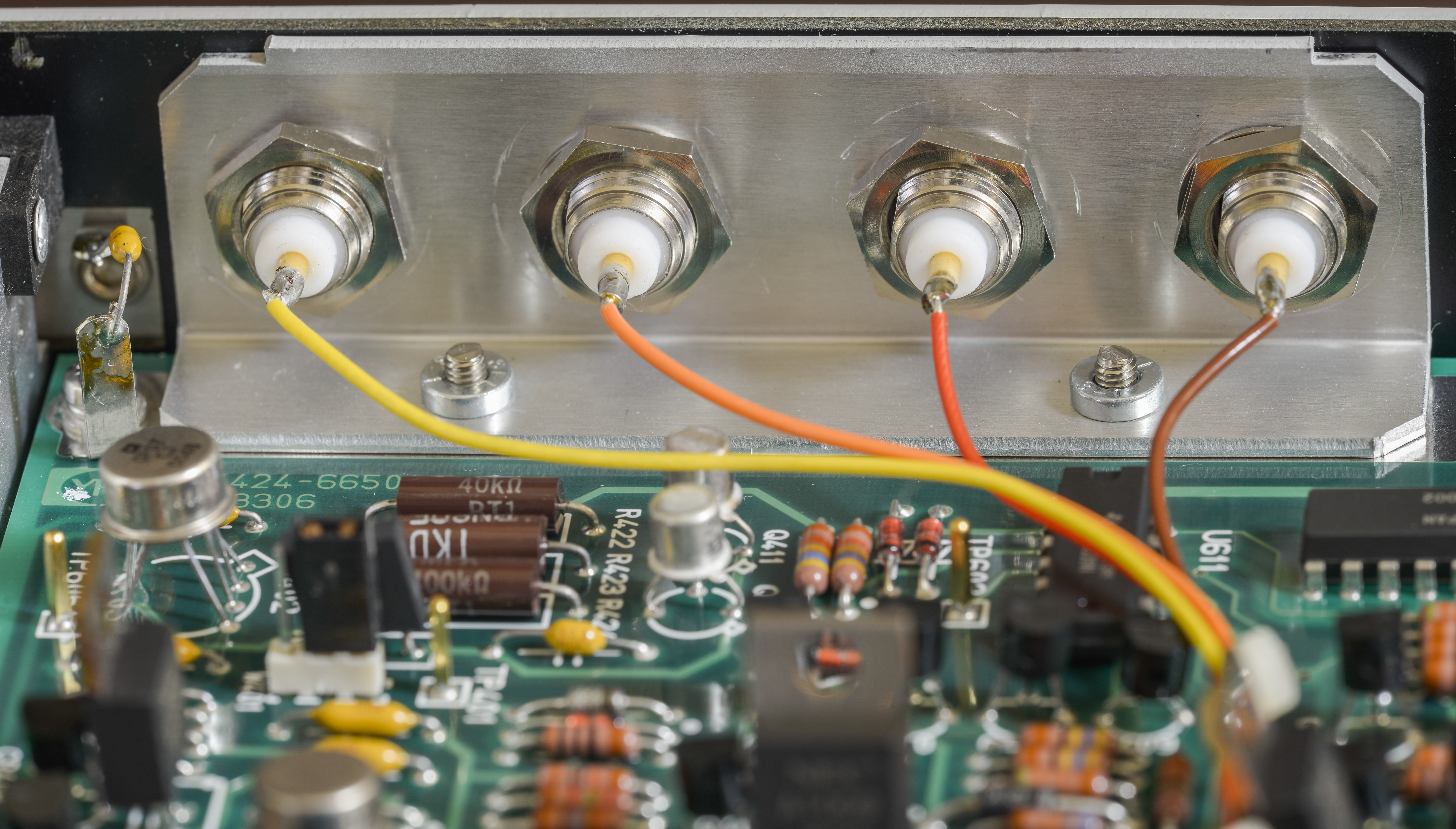
All connections from them routed using regular unshielded wire to related parts of circuitry on the PCB. Connection done via low-leakage shielded reed relays and teflon standoffs to ensure low leakage in off condition.


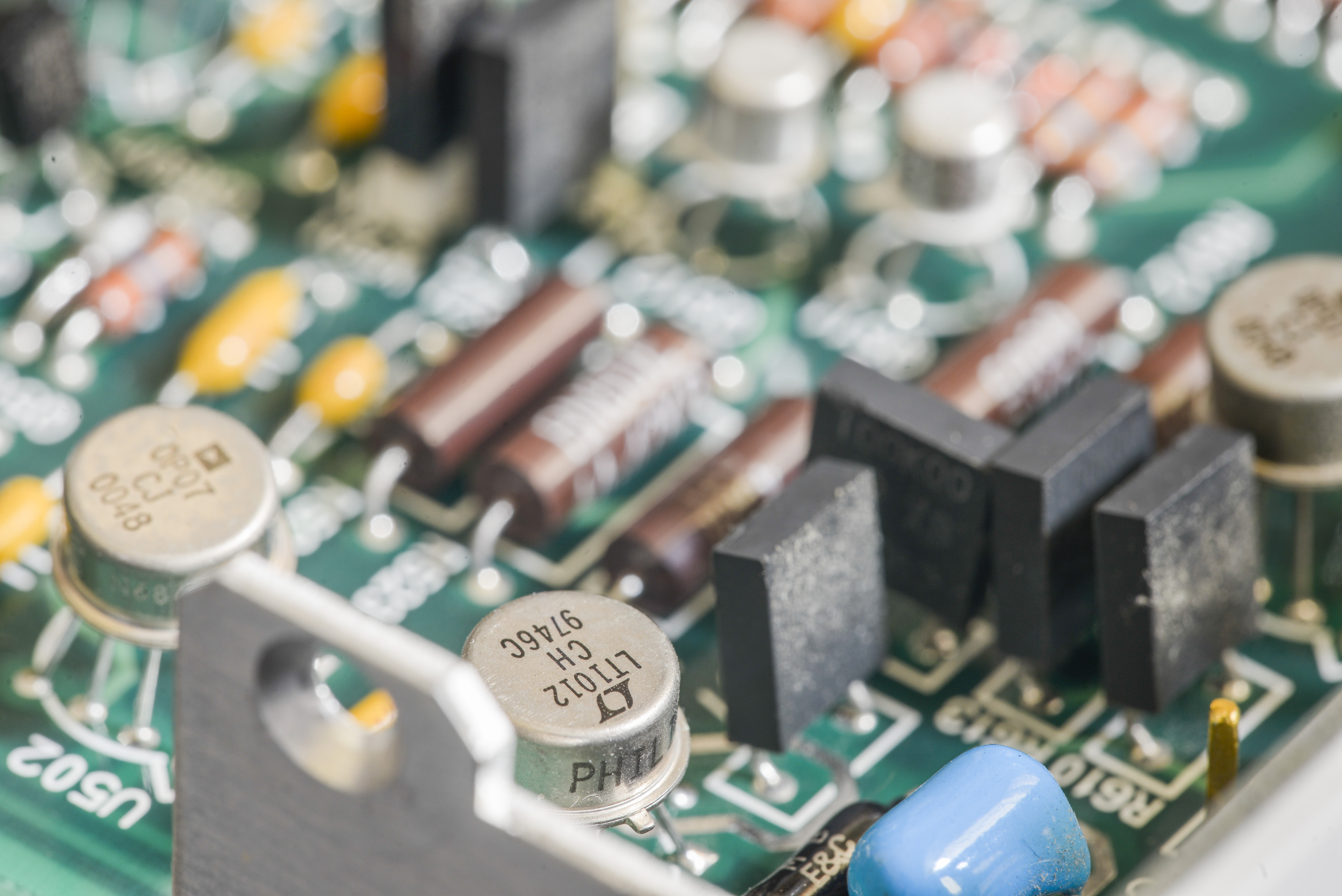
Some more photos of these parts are made:

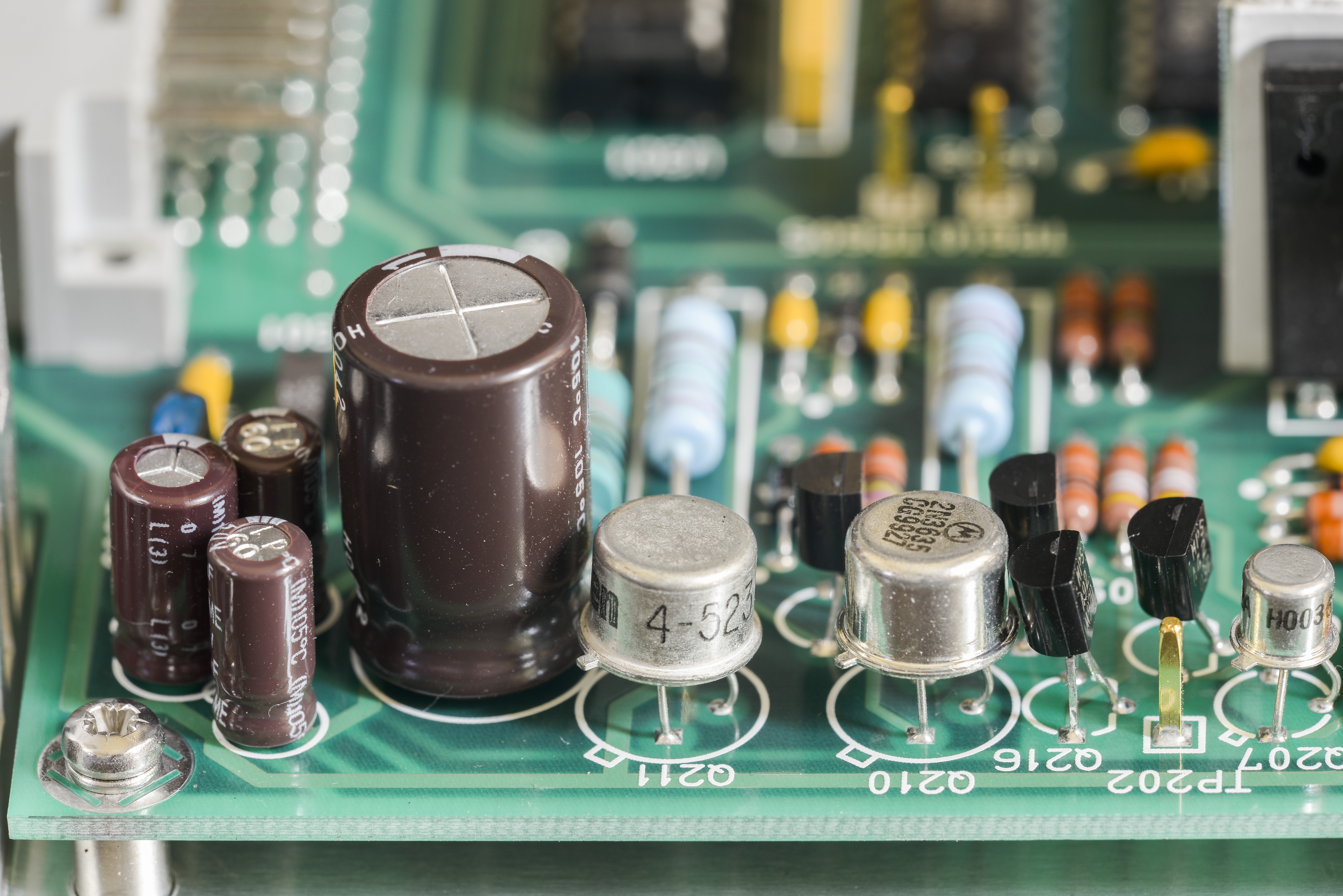
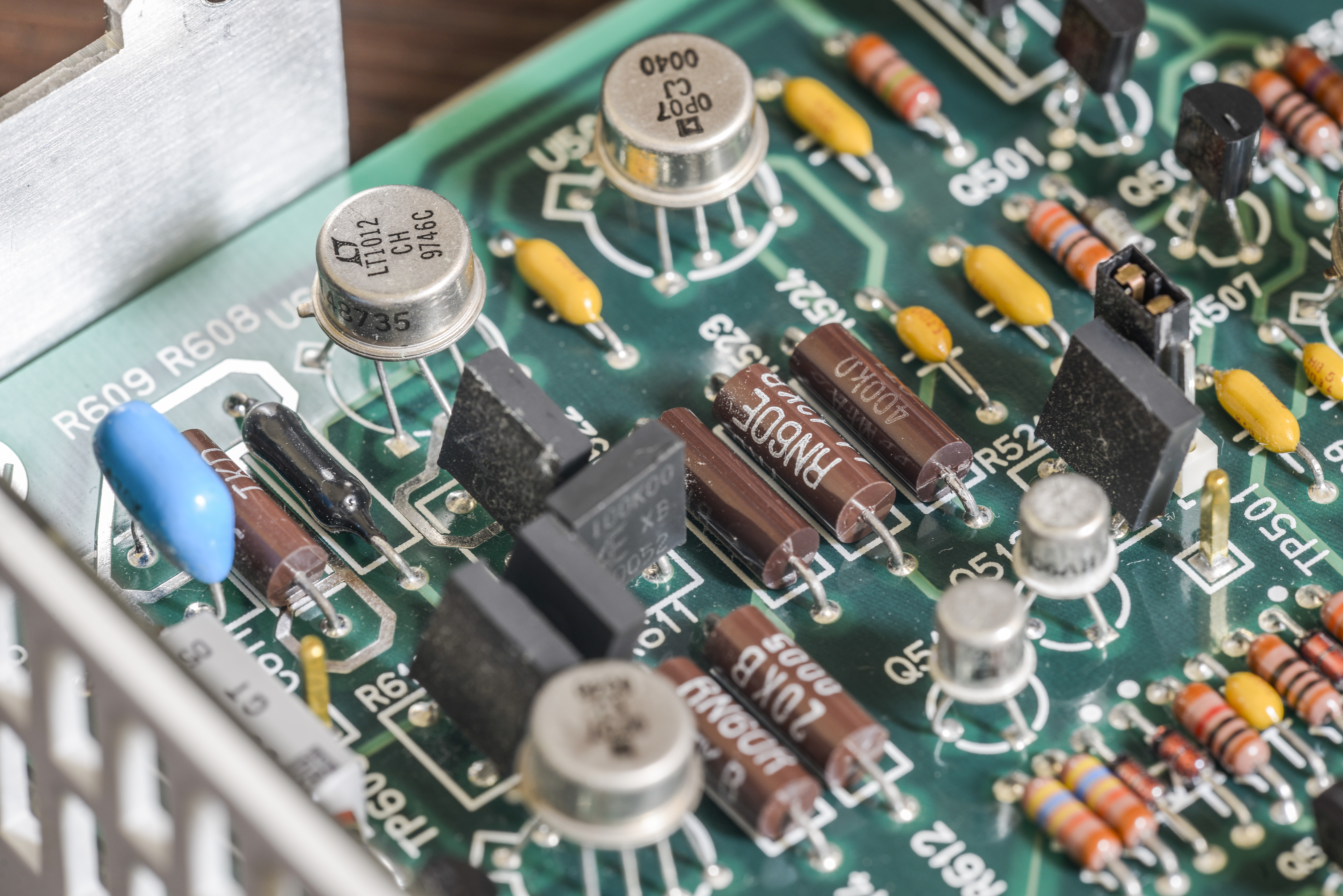
Central high-power transistors are mounted on aluminum block, which couples to module cover via thermal grease contact. There are some OP07CJ and LT1012CH operational amplifiers and guard traces around on PCB to keep circuit operation stable and within spec.

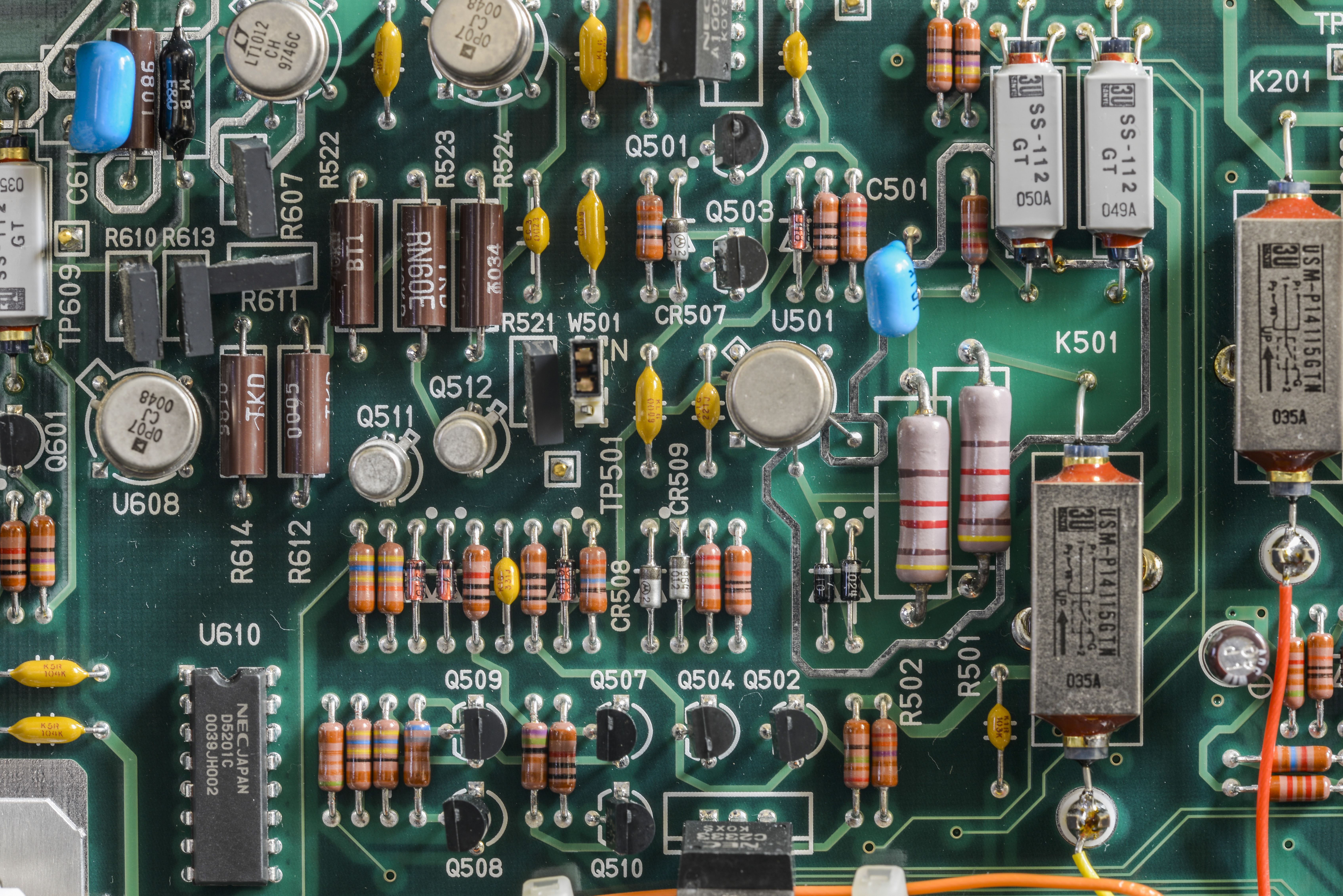

Pair of DACs together with related components
Some of operational amplifiers are AD711AH in metal hermetic TO package.


Interface connector to the mainframe is same as rest of the 4142x modules, single 4-row Eurocard connector with some pins unpopulated. Look at that copper springs at the edge, they look like brand new.
AE foil resistors founded on this module as well:
| RefDes | _ Resistor Type | Value |
|---|---|---|
| R421,R521,R613,R610,R607,R521 | AE XB | 100.00 KΩ |
| R135 | AE XQ | 40.000 KΩ |
| R108 | AE XB | 5.7340 KΩ |
| R106 | AE XA | 5.1230 KΩ |
| R109 | AE XA | 80.000 KΩ |
| R137 | AE XB | 16.000 KΩ |
| R110 | AE XA | 19.980 KΩ |
| R140 | AE 0L1 | Network 4 pin |
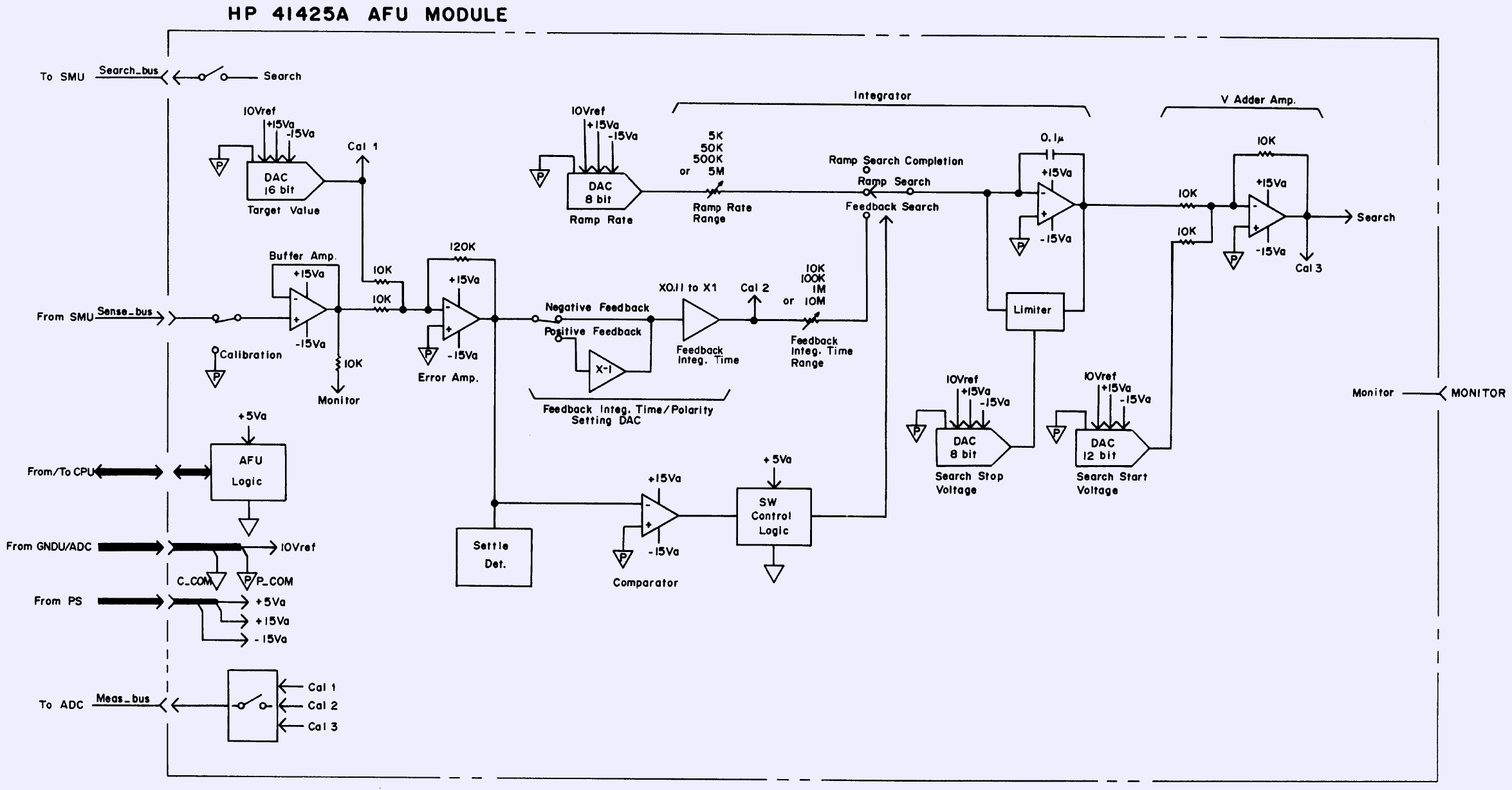
HP 41425A Analog Feedback Unit
This module takes 1 slot in 4142B and does not have external interfaces.
Block diagram
Repair
No repair required, everything works normally, clean and nice.
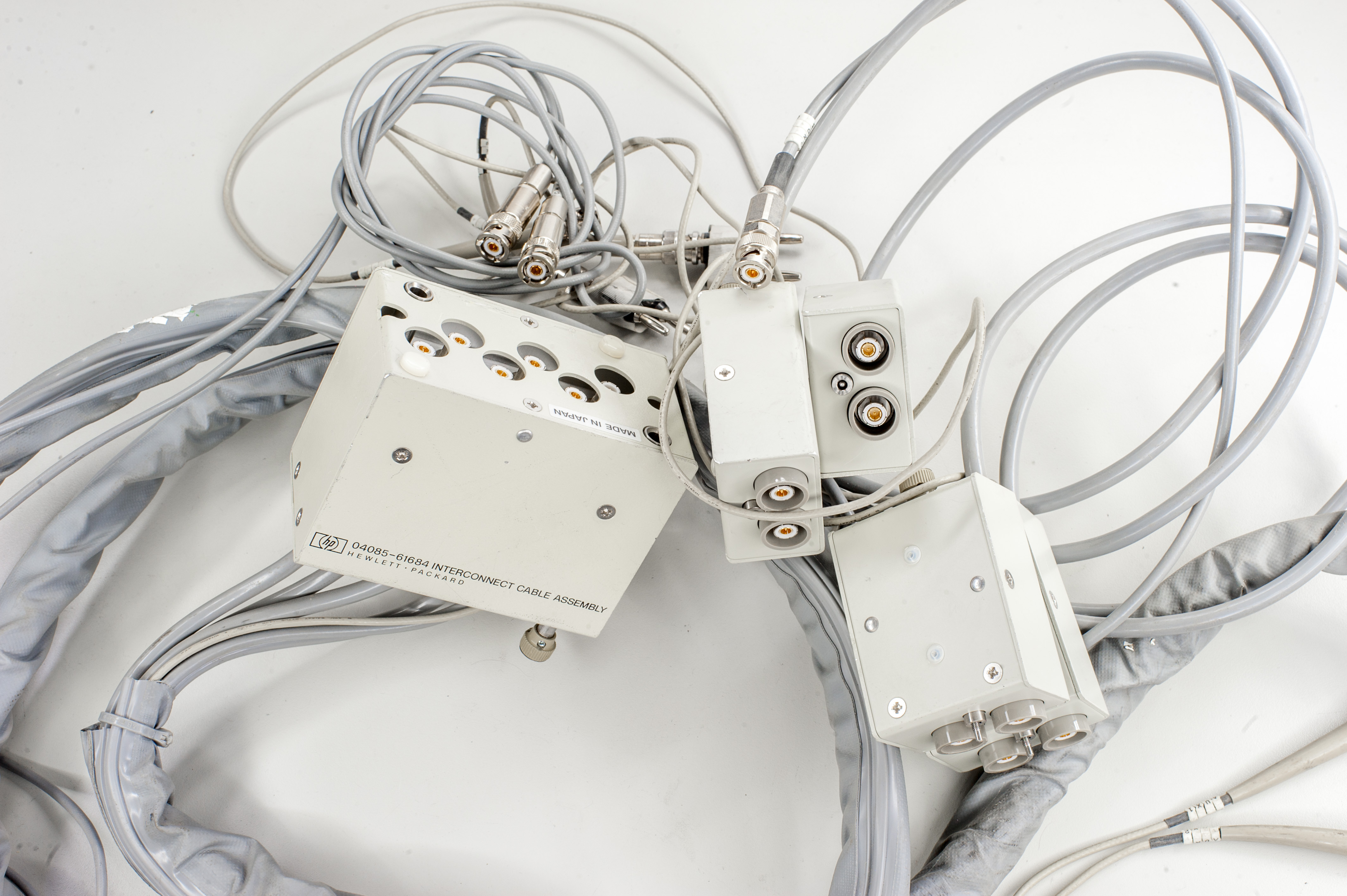
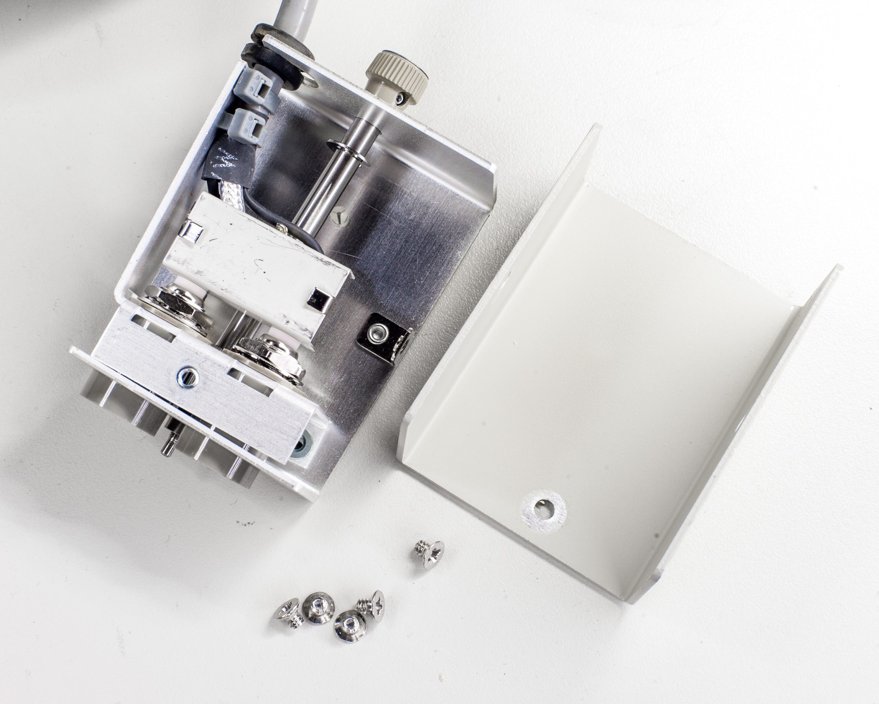
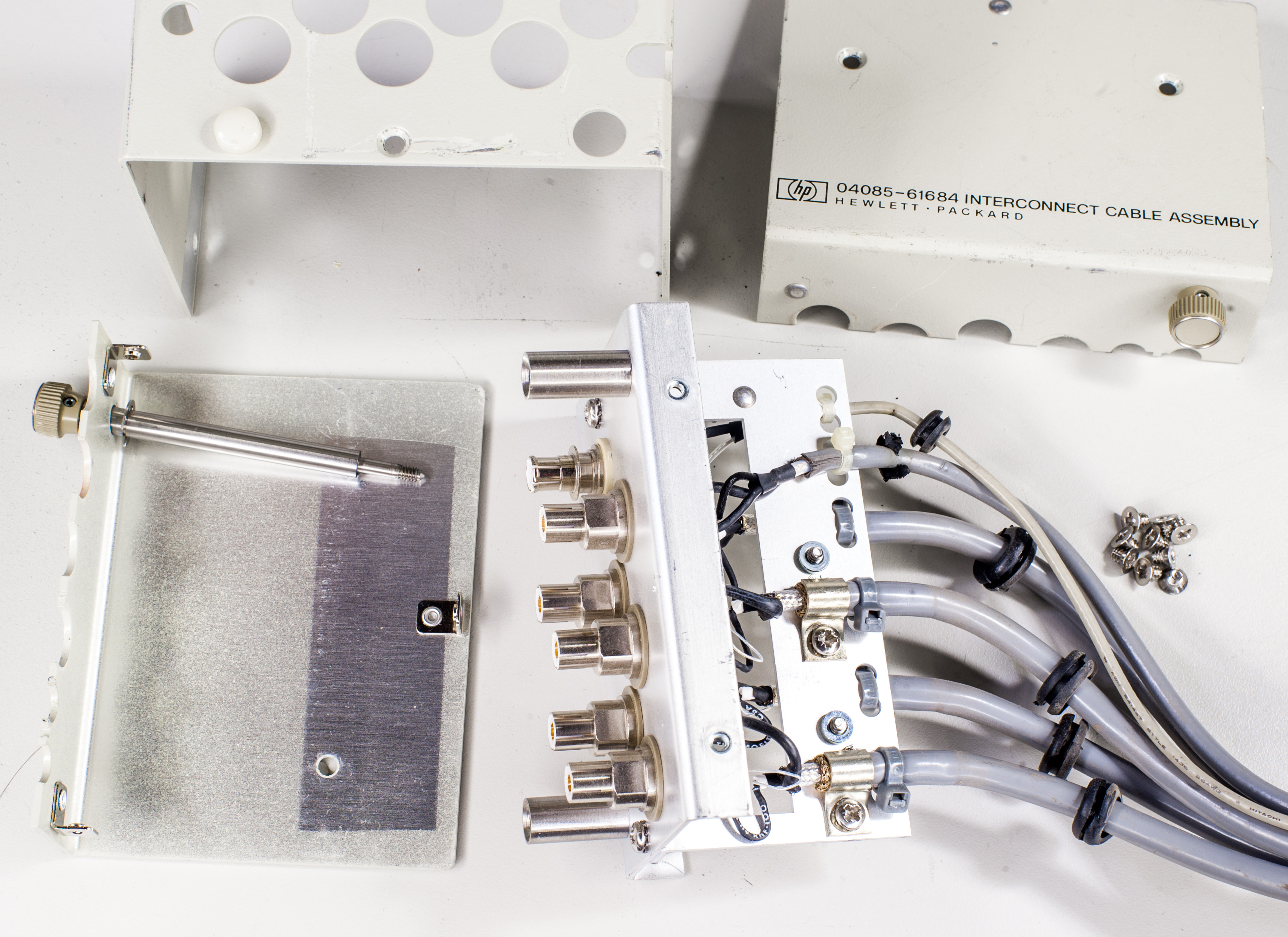
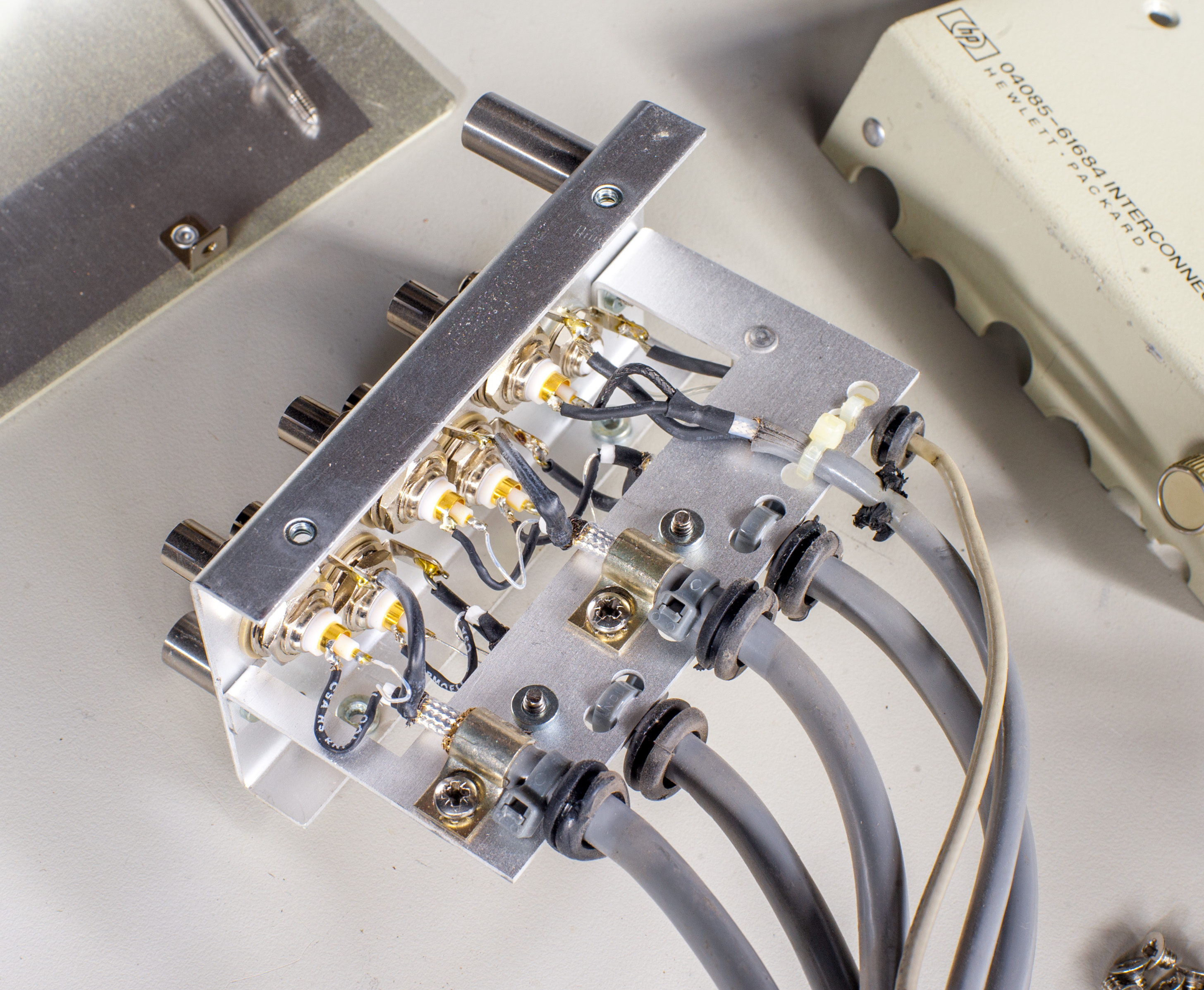
HP 4085-61684 triax cable assembly from HP 4062UX system

This cable designed to connect 4142B with four SMU modules and one VM/VS module to the HP 4085B semiconductor analyzer switch matrix.
Firmware
Unit running firmware version 4.30, according to GPIB response on [**IDN?*] command.
Rev.4.30 HP 4142B firmware dump files
| Firmware bank | ROM1 | ROM2 | ROM3 | ROM4 |
|---|---|---|---|---|
| Bank A | 04142-85020 binary | 04142-85021 binary | 04142-85022 binary | 04142-85023 binary |
| Bank B | 04142-85030 binary | 04142-85031 binary | 04142-85032 binary | 04142-85033 binary |
| Bank C | 04142-85038 binary | 04142-85039 binary | ||
| Bank D | 04142-85124 binary | 04142-85125 binary | 04142-85126 binary | 04142-85127 binary |
| Bank E | 04142-85144 binary | 04142-85145 binary |
Testing
Unit is taking 4W of power during stand-by operation and about 80W of power when idle with current set of modules installed.
I also connected some test wires to check main voltage reference output, using my trusty HP 3458A.
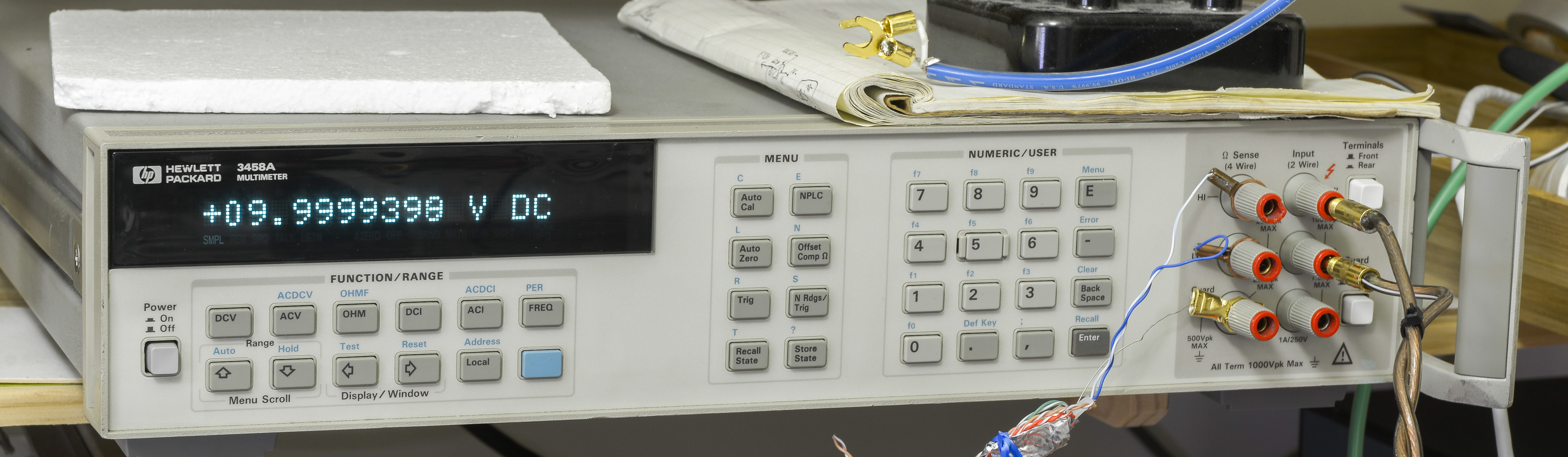
Before calibration reference output was pretty accurate, at 9.99994 VDC.
Very minor adjustment of trim resistor near reference allowed to get us 10.000005 VDC.

Some of example experiments shown in appnote
Software
HP 4142B was designed around HP computer systems and all programs shown in appnotes and manuals are targeted for BASIC platform. Since today computer world changed a lot since 90’s, we will try to use Python and linux-gpib to get same functionality from the device.
First I ran ibtest program to check if Raspberry Pi with linux-gpib package can talk with the instrument and read data back.
enter a string to send to your device: *IDN?
sending string: *IDN?
trying to read 40 bytes from device...
received string: 'HEWLETT PACKARD,4142B,0,4.30'
Identification works well, let’s see information about installed modules:
enter a string to send to your device: UNT?
sending string: *IDN?
trying to read 200 bytes from device...
received string: '0,0;HP41421B,3;0,0;HP41424A,1;0,0;HP41424A,1;0,0;0,0'
But first attempt of using it with usual Python binding thru linux-gpib rendered no good results, 4142B just entering TALK mode and does not feedback or execute any commands. This was due to lack of proper EOF for 4142B.
After adding \n into command strings, everything work like expected.
Test application in Python:
# xDevs.com Python test GPIB app
# http://xdevs.com/fix/a4142b/
import sys
import Gpib

inst = Gpib.Gpib(0,14) # 4142B GPIB Address = 27
inst.clear()
inst.write("*RST\n")                              # Reset instrument
inst.write("*IDN?\n")                             # Request ID command
str = inst.read(40)
print str
Response from the instrument:
root@pi2:# python ./cvr.py
HEWLETT PACKARD,4142B,0,4.30
Now we can port some BASIC applications from application notes and try running experiments using this Agilent 4142B.
Transistor leakage experiment
Capacitor leakage experiment
Zener I-V experiment
Dielectric Absorption measurement experiment
Capacitors used in integrating and high-resolution A/D circuits, such as multislope ADCs have tight requirements for low DA. Using parametric analyzer is one way of testing this parameter in capacitors.
Setup configuration for this experiment:
- 41424B MPSMU module as voltage source
- GNDU as current sink/reference
Summary
Project cost:
| Item | Cost | Shipping | Supplier |
|---|---|---|---|
| Agilent 4142B + 41421B + 2×41424A | $225 | $250 | Yahoo auction |
| HP 41425A | $40 | $50 | eBay |
| Broken HP 41420A | $50 | $55 | eBay |
| Used good HP 41420A | $50 | $15 | eBay |
| Used good HP 41420A | $49 | $30 | eBay |
| Used good HP 41420A (may fail self-test) | $24 | $25 | eBay |
| Used good HP 41425A | $25 | $15 | eBay |
| Interconnect cable assembly HP 04085-61684 | $78 | $35 | eBay |
| Total | $621 | $475 | $1096 USD |
Decent prices on acquired modules and mainframe are due to lack of commercial interest, obsoleted software with zero support on modern platforms. However it does not prevent interested hobbyists to enter this interesting SMU world without paying thousands for modern variants like Keithley 24xx/26xx SMU.
This 4142B system will be used for various experiments with operational amplifiers and circuits evaluation and component testing in xDevs.com lab, so stay tuned for more articles.
If you have questions or corrections, please let us know in comments.
Projects like this are born from passion and a desire to share how things work. Education is the foundation of a healthy society - especially important in today's volatile world. xDevs began as a personal project notepad in Kherson, Ukraine back in 2008 and has grown with support of passionate readers just like you. There are no (and never will be) any ads, sponsors or shareholders behind xDevs.com, just a commitment to inspire and help learning. If you are in a position to help others like us, please consider supporting xDevs.com’s home-country Ukraine in its defense of freedom to speak, freedom to live in peace and freedom to choose their way. You can use official site to support Ukraine – United24 or Help99. Every cent counts.
Modified: Oct. 31, 2017, 4:51 a.m.