Contents
- Intro
- Disclaimer
- Manuals and service information
- Restoration of xDevs Datron/Wavetek 4910 DC standard
- Front panel posts restoration
- Battery cells power pack
- Datron 4910 Motherboard repairs
- Rear panel powersupply PCBA
- Reference Cell LTZ1000CH PWMDAC 10 V modules, DOM 1994
- Output buffer and 1V/1.018V divider PWMDAC/timing module, DOM 1994
- Repairs summary with discovered bad parts
- First datalog after reassembly
- More detailed performance benchmarks after repair
- Using Datron 4910 for external calibration transfers
- Datron 4912 Teardown
- Long-term stability measurements for xDevs Datron 4910
- Summary and conclusion
![]()
![]()
![]()
![]()
![]()
![]()
![]()
![]()
![]()
![]()
![]()
![]()
![]()
![]()
![]()
![]()
![]()
![]()
![]()
![]()
![]()
![]()
![]()
![]()
![]()
![]()
![]()
![]()
Intro
DC voltage standards in Datron 4910 family include three models. Fully featured 4910 feature 4-cell SSR with optional outputs while stripped 4911 (w/o 1V/1.018V divider) and 4912 (single cell only) are lower cost options. These 4910 DC reference standards developed by legendary John Pickering and his team were competing with old Fluke units and were among the first ones to work as robust replacements to the fragile and sensitive Weston cells. All 491x can provide stable 10 V DC Voltage output with a typical stability of better than 1 µV/V per year. Each unit features internal battery pack out of eighteen 6 V 2 Amp*hour lead-acid cells with long life transit mode which makes it a great option for transfer applications and metrology use. Accuracy setting resolution of this standard is between 0.1 µV/V – 0.2 µV/V. The operating temperature range is specified at 0 °C to +40 °C. Temperature coefficient of a 10 V averaged output and cell specified at 0.05 µV/V/°C.
Each cell in Datron 491x is a separate isolated unit, each of which based around LTZ1000CH super-zener and is a direct competition to Fluke’s 734 reference system, which consist of four more modern Fluke 732B or 732C modules. Datron 4910 was designed prior to Fluke acquired company’s assets, it’s likely that Fluke got inspiration from 4910 to make a 734A product after seeing how powerful and useful is the multi-cell output like implemented in Datron 4910. Fluke used their own Motorola-designed reference amplifier (SZA263) and later Linear Technologies LTFLU-1 REFAMP, both of which can be found in many of Fluke’s products from DMM’s, calibrators, and voltage references. Fluke relied on a high performance resistor networks, bulky external ovens and extensive thermal shielding to isolated sensitive zener circuit from environment variations.
Datron went a different route here. They chose a commercially available voltage reference, the Linear LTZ1000. This LTZ1000 chip has decades of history and is considered as the best available buried zener reference by many engineers. Outstanding specifications of the 4910 series standards also show how competitive it is. Datron/Wavetek references also implemented LTZ1000 into many of their other high end test equipment. They can be found in the 1271/1281 DMM’s, the 4920 AVMS, and in their multifunction calibrators like the 4708 and even early production units of Fluke 8508A DMM. It was a departure from Datron’s older original designs where they chose several zener diodes and matched their tempco to provide a reference that was stable with both time and temperature.
Image 1. 4910 DC Standard reference core block schematics
Second Datron’s major departure in design hides in way 4910 scale output voltages to nominal 10 V and 1 V/1.018 V. Common reference zener DC standards utilize expensive high-end resistance elements in hermetic packages to amplify/divider voltages to desired levels, relying on long-term stability and very low temperature coefficients of such resistors to deliver good performance. While failures of such resistors are not common this approach does significantly increase cost of implementation and production of DC voltage standards. Datron 4910 instead utilize digital method to amplify/divide voltages with low frequency PWM with help of timing circuits, moderately good scaling resistors and extensive output filtering. Somewhat similar method is also used in some other metrology products such as Fluke 5700A, newer Fluke 5720A and 5730A calibrators, Fluke 5790A AC/DC voltmeters and Valhalla 2720GS DC calibrator.
Image 2. Front panels of all three Datron 491x family members
In this article we will restore a full-featured 4910 to it’s glory and also take a look on rare Model 4912. They are of a similar size and weight to the Fluke 732A and were in direct competition for short time. Special Datron 4912 differs from the 4910/4911 due to limited single “cell” output. Just like fully featured Datron 4910 this special Datron 4912 also includes a low impedance 4-wire output plus divided outputs at 1V and 1.018V. Unlike 4912 other two models include all four “cell” outputs with the capability to average them together, or even build higher voltage outputs like 20 V, 30 V or 40 V since each output can be fully floated and isolated.
| Specification | Fluke 732A | Fluke 732B | Fluke 732C | Fluke 734A or 734C | Datron 4910 | Datron 4911 | Datron 4912 |
|---|---|---|---|---|---|---|---|
| Output voltage, DC | 1V, 1.018V, 10V | 1.018V, 10V | 0.1V, 1V, 10V | 4 × 732B or 732C | 4 × 10V, 10V average, 1.018 V, 1.000 V, buffered 4-wire | 4 × 10V, 10V average | 1 × 10V, 1.018V, 1.000V, buffered 4-wire |
| Stability (30 day, 10V) | ±0.5 µV/V | ±0.3 µV/V | <±0.3 µV/V | ±0.3 µV/V | ±0.3 µV/V | ±0.3 µV/V | |
| Stability (1 year, 10V) | ±6 µV/V | ±2 µV/V | <±2 µV/V | ±1 µV/V | ±1 µV/V | ±1.5 µV/V | |
| Temperature coefficient, µV/V/K | ±0.05 | ±0.04 | ±0.04 | <±0.05 | |||
| Adjustment range | 50µV, 5 µV/V | BCD switches | No adjustment | PWMDAC switches | |||
| Reference design solution | Motorola SZA263 | LTFLU-1 | up to 4 x Linear LTZ1000CH, one per cell | ||||
| Max load current | 12 mA | 12 mA | 15 mA for buffer output only | ||||
| Output noise | <1 µVRMS, 0.1-10Hz | <0.6 µVRMS, 0.1-10Hz | <0.4 µVRMS, 0.1-2 Hz | ||||
| Construction type | Rugged half-rack module | Rugged ¼-rack module | Full-width 19” rack frame | Rugged half-rack module | |||
| Active thermal compensation | Yes, +45° C oven assembly | LTZ1000 internal on-chip oven | |||||
| Temperature sensor for monitoring | Yes | No | |||||
| Operation range, ambient | +0…+40 °C | ||||||
| Power requirements | 100,120,220,240VAC or 24-40VDC | 100,120,220,240VAC or 12 VDC | 100,120,220,240VAC or 10-40 VDC | ||||
| Backup/offline power supply | Internal ±12V Battery bank, 12 hours life | Internal ±12V Battery bank, 72 hours life | ±18V 15pcs battery array, 168 hours life transit mode | ||||
| Dimensions, weight | 603 × 221 × 191 mm, 12.3kg | 254 × 206 × 311 mm, 4.8kg | 591 × 214 × 182 mm, 20 kg | ||||
| MSRP | ~$2k USD [1984, EOL] | $9k USD [EOL] | $16k USD | $60k USD | $8k+ USD [1990, EOL] | ||
Disclaimer
Redistribution and use of this article or any images or files referenced in it, in source and binary forms, with or without modification, are permitted provided that the following conditions are met:
- Redistributions of article must retain the above copyright notice, this list of conditions, link to this page (https://xdevs.com/article/d4910/) and the following disclaimer.
- Redistributions of files in binary form must reproduce the above copyright notice, this list of conditions, link to this page (https://xdevs.com/article/d4910/), and the following disclaimer in the documentation and/or other materials provided with the distribution, for example Readme file.
All information posted here is hosted just for education purposes and provided AS IS. In no event shall the author, xDevs.com site, or Datron/Fluke or any other 3rd party be liable for any special, direct, indirect, or consequential damages or any damages whatsoever resulting from loss of use, data or profits, whether in an action of contract, negligence or other tortuous action, arising out of or in connection with the use or performance of information published here.
If you willing to contribute or have interesting documentation to share regarding pressure measurements or metrology and electronics in general, you can do so by following these simple instructions.
Manuals and service information
Datron 4910/4911 User’s Handbook
Datron 4910/4911 Service manual 1991 w/schematics
Datron 4910/4911 Service manual 1990 w/schematics
Separate pages for Cell schematics, part 1
Separate pages for Cell schematics, part 2
Separate pages for Cell schematics, part 3
Separate pages for Cell schematics, part 4
Separate pages for Clock schematics, part 1
Separate pages for Clock schematics, part 2
Datron application note explaining PWMDAC approach
There is no manual currently available for the 4912 so the 4910/4911 manual can be used for troubleshooting.
Some additional community-generated files also available to aid understanding of 4910 design, especially LTZ1000CH-zener cell modules.
Service for D4910 by master Lymex
Schematics reverse engineered for zener module
Schematics clone for VHD variant of zener module
Schematics clone for VHD variant of zener module
Gerber file for VHP/VHD zener module
Gerber file for 7-10V PWM module cell
Restoration of xDevs Datron/Wavetek 4910 DC standard
In February 2026, a good decade since this article was first drafted up at xDevs HQ we finally got our very own Model 4910 for lab. Standard arrived in a poor non-working condition, ruined front terminals and typically dead batteries. We’ll attempt a full restoration and document the progress in this article. Datron 4910 these days can be acquired only from secondary market and it’s common to expect them in poor shape due to it’s previous life adventures. Fluke killed 491x series in favour of their 732B standards shortly after Wavetek acquisition and merger.
Image 3. Front panels of patient Datron 4910 for restoration
All front binding posts in this example are damaged and heavily discolored by exposure to sun or heat over long duration. These posts aren’t good design in the first place even new. CELL 2 LO and 1.018 V HI terminals are sheared completely off, only leaving useless stub. Every single post base is fractured and discolored badly. Binding posts resemble modern low quality Pomona 3770 connectors but actually made by unrelated company in England.
Front panel posts restoration
Image 4. Front panel with bad posts
Removing front panel was pretty easy as whole front assembly held by two screws and connected to 4910 mainboard by DIN dual-row interconnects.Rear side shows few labels with front PCBA part number 400880-2.0 880/025/001, tested on 7/10/1994 by IDH.
Image 5. PCBA of the front panel
Each HI/LO pair output coupled with passive RC network and gas discharge tube to arrest any static from external world. Each binding post making contact to gold-plated PCB pads with gold-plated washer and gold-plated nut.
Image 6. Front panel assembly with PCBA and original connectors
Removing few nuts revealed some green copper oxide crust that definately warrant full cleaning process with abrasive materials, even before we install new binding posts.
Image 7. Crusty corrosion and oxidation around binding post threads
PCB area around LEDs show clearly visible discoloration due to years of heat generated by diodes.
Image 8. PCB discoloration around LEDs
Perhaps I’ll replace those LEDs to something modern and lower power to make it nicer :)
Image 9. Shined front panel PCBA
Additional isolation PCB was hiding under front panel electrical PCBA, since binding posts were not equipped with rear insulation washer. Yet another reason to replace these posts to get better insulation from case metal front panel block.
Image 10. Isolation PCB for binding posts fixturing
Close-up on original binding posts, manufactured by Cliff Electronic Components, similar to modern TP1 model.
Image 11. Close-up on cracked plastic
They are somewhat similar to low quality Pomona 3770 terminals but not mechanically identical.
Image 12. Disassembled and removed binding post
All of these must go, no questions asked here.
Image 13. Original colored plastic insulators with posts removed
Original front panel metal case has cutout indents to prevent post from turning around when mounted on front-panel.
Image 14. Mount holes with key notch in cast metal panel
Markings and face labels are on decorative metal plate P/N 450751-4, stuck to metal casting panel with a strip of double-sided adhesive.
Image 15. Label plate rear side
Drilling holes was simple as the metal panel is made out of soft aluminum sheet. Edges had to be deburred with a knife to ensure smooth edge.

Image 16. Cleaned up front panel label plate
Same drilling was done for both face panel and front panel metalwork.

Image 17. Front panel ready for new posts
All edges were deburred and cleaned up prior to installing insulators and posts.

Image 18. Rear side all cleaned and ready
So first action was to replace them with something robust and nicer. After few trials and xDevs inventory checks I’ve decided to go with special order bare copper terminals with PTFE insulation washers.
Image 19. Ideas for new binding posts replacement
Image 20. Cleaned up front panel label plate
Same drilling was done for both face panel and front panel metalwork. All edges were deburred and cleaned up prior to installing insulators and posts. Best option is to avoid any plating and to maintain good interface with bare copper surfaces and lowest possible parasitic thermal EMF.
p=. 
Image 21. Test fit with PTFE post
Each of these posts would need minor drilling out of metalwork for fitment and removal of insulation PCB as now PTFE rings will provide increased spacing to main front PCBA.
Image 22. Test mount with copper nut in place
These should do the job nicely and they are well tested for nanovolt-grade signals.
Image 23. New binding posts with insulators
And here’s look with all posts installed for test fit:
Image 24. All fitted on the front panel
Main cell outputs all used longer posts to fit double nuts for extra security for nanovolts.

Image 25. All electrical connections with pure copper nuts
I’ve also cleaned up rear PCB surface with sandpaper a bit.

Image 26. Rear with new posts in place
Holes were drilled little bigger to fit the PTFE insulation washer from bare copper posts.
All done and ready:

Image 27. Updated front panel looks on 4910
Much cleaner and nicer. I’ve cleaned and reused original gold-plated shorting bars for 4-wire output buffer and guard-case terminals.
Battery cells power pack
Next step is to acquire brand new lead acid batteries and rebuild the battery unit so standard can be ran without AC power for testing and backup power use. There are 18 batteries in five groups each. Each group equipped with temperature sensors and protection fuses for additional safety in operation.

Image 28. Battery pack schematics
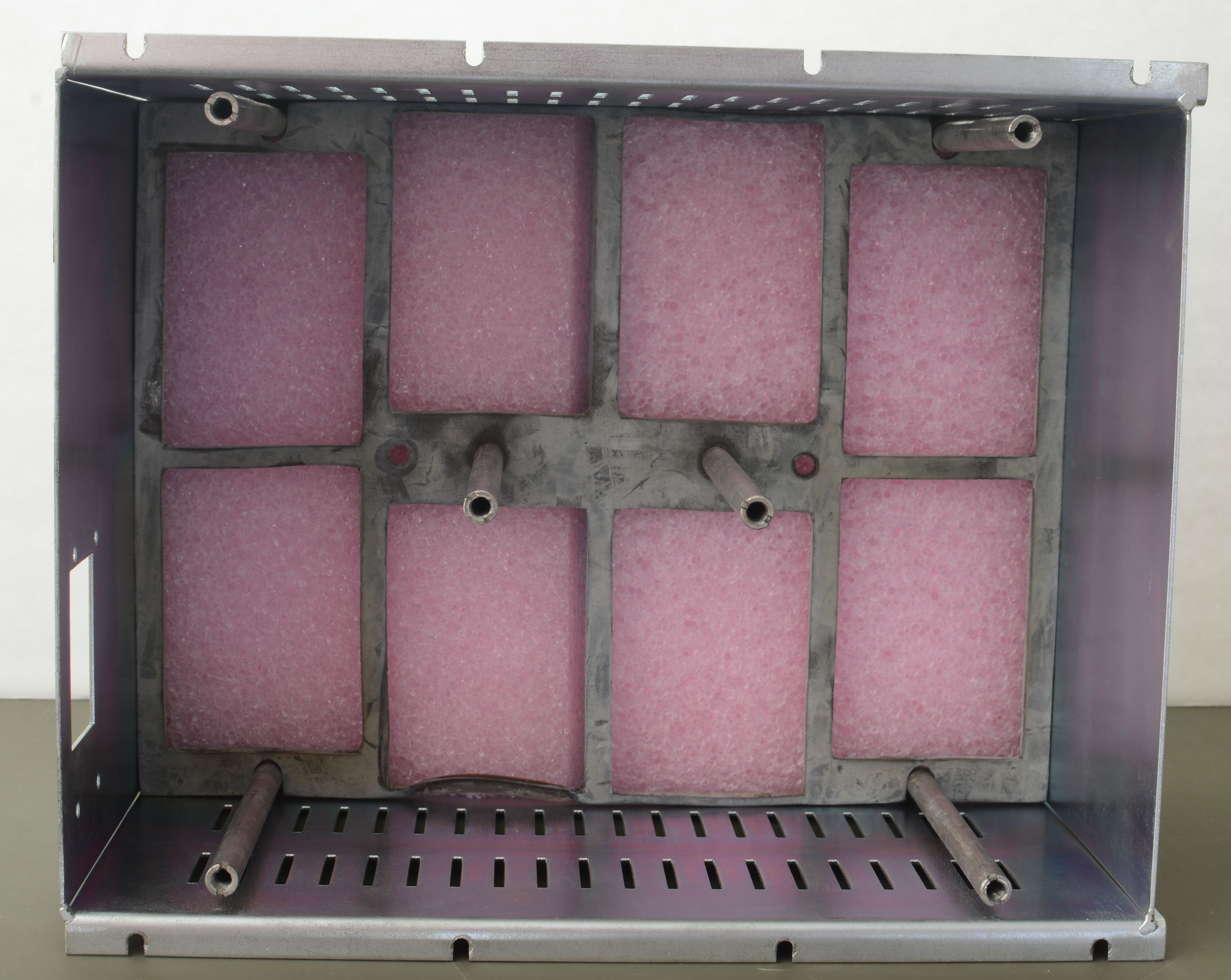
Whole pack is enclosed in removable steel box module to provide easy field replacement for user if needed.

Image 29. Metal battery module case
Connections to rest of the instrument is done with two D-Sub connectors. Red insulator 15-pin one provides positive voltage connections, while black 9-pin returns grounds to negative sides of each battery group.

Image 30. D-Sub battery interface

Image 31. Batteries kept at two layers to save space
Original batteries that 4910 used in design are obsoleted long ago so modern smaller size need to be retrofitted instead.

Image 32. New batteries
To replace old dead accumulators I’ve bought 15 pcs brand new Powersonic PS-621. These have same capacity as originals and should work equally well.

Image 33. Replacement batteries
I’ve sorted batteries by their voltage and change level into groups, since they are used in 3S arrays with total of 5 arrays.

Image 34. Test fit with one battery
Good idea to have additional spacer around each battery to prevent them moving around in assembled pack.

Image 35. Some corrossion on metalwork before cleaning
I’ve used hard scotchbrite abrasive pad and some alcohol to get rid of most surface corrosion and grime on metal parts. This process shown in report video about this 4910, linked down below in this article.
Here’s finished battery pack after cleaning and batteries replacement. Hopefully it will live well until estimated service four years from now in 2030.

Image 36. Cleaned, assembled and tested battery module
Ready to install into the chassis.

Image 37. Good idea to put a label stating when battery was installed and what’s due
Be sure to check every battery array output for proper polarity and voltage at the output DSub connectors. Schematics is the most helpful to identify required pins which are:
- Pack 1, +18 V nominal for Cell 1 = pins J9.1 (BLACK) and J8.1 + J8.2 (RED)
- Pack 2, +18 V nominal for Cell 2 = pins J9.2 (BLACK) and J8.10 + J8.11 (RED)
- Pack 3, +18 V nominal for Cell 3 = pins J9.3 (BLACK) and J8.4 + J8.5 (RED)
- Pack 4, +18 V nominal for Cell 4 = pins J9.4 (BLACK) and J8.13 + J8.14 (RED)
- Pack 5, +18 V nominal for Divider/timing outputs = pins J9.9 (BLACK) and J8.7 + J8.8 (RED)
It’s important to verify correct polarity for each battery group to avoid damage to power regulator circuitry.
Datron 4910 Motherboard repairs
Next repair step was to check and service power regulators and power supply rails on motherboard. Old test equipment commonly develop faults in power filter/regulation circuits which can often cause cascading failures for various functions and blocks. To address this I usually replace all electrolytic, thru-hole tantalum capacitors, carbon resistors and then test each regulator for compliance with expected specs and noise. There is no point to worry about affordable components for a repair of expensive and valuable instrument like this, so I don’t even bother to check or measure old original parts, unless it’s something special.
Let’s take a look on the mainboard top view:

Image 38. Mainboard backplane
This board has DIN and Dsub connectors for each cell module, five independent linear voltage regulators, monitoring circuitry for DC input and interconnect to front panel PCBA. PCB extends across whole length of the instrument and has just two copper layers. Blue multi-pole switch is used to toggle between normal fully powered state and trasit state when power is cut to all non-essential circuits to save battery life in shipping.

Image 39. Bottom side of the mainboard backplane
This monster multi-pole switch that selects power path for all battery packs between normal mode and transit mode probably a custom job for Datron as I never seen similar switches before. Hopefully I wouldn’t need to clean it :)

Image 40. 8-level switch assembly

Image 41. Backlit photo of motherboard circuits
Datron service manual provides us with description of various useful test points and expected voltages on board board. Table 2.2.11 is reproduced below with my own measurements before and after repairs:
| Supply | Test points | Specification | Drawing | As received | As repaired | |||
|---|---|---|---|---|---|---|---|---|
| without battery | with battery | without battery | with battery | without battery | with battery | |||
| I+ (1) | TP102 vs TP101 | 24.5 VDC ±0.5V | 20.6 VDC ±0.25V | DC400878 Sheet 1 | 25.39 V | 21.73 V | 24.16 V | 20.60 V |
| I+ (2) | TP202 vs TP201 | 24.5 VDC ±0.5V | 20.6 VDC ±0.25V | DC400878 Sheet 2 | 25.06 V | 21.33 V | 24.26 V | 20.60 V |
| I+ (3) | TP302 vs TP301 | 24.5 VDC ±0.5V | 20.6 VDC ±0.25V | DC400878 Sheet 3 | 27.54 V | 23.23 V | 24.01 V | 20.61 V |
| I+ (4) | TP402 vs TP401 | 24.5 VDC ±0.5V | 20.6 VDC ±0.25V | DC400878 Sheet 4 | 24.70 V | 20.96 V | 24.31 V | 20.61 V |
| I+ (5) | TP502 vs TP501 | 24.5 VDC ±0.5V | 20.6 VDC ±0.25V | DC400878 Sheet 5 | 26.60 V | 22.87 V | 24.02 V | 20.61 V |
| +12V REG (1) | TP104 vs TP101 | 12 VDC ±0.6V | DC400878 Sheet 1 | 12.21 V | 12.21 V | |||
| +12V REG (2) | TP204 vs TP201 | 12 VDC ±0.6V | DC400878 Sheet 2 | 12.19 V | 12.19 V | |||
| +12V REG (3) | TP304 vs TP301 | 12 VDC ±0.6V | DC400878 Sheet 3 | 12.28 V | 12.29 V | |||
| +12V REG (4) | TP404 vs TP401 | 12 VDC ±0.6V | DC400878 Sheet 4 | 12.39 V | 12.36 V | |||
| +12V REG (5) | TP504 vs TP501 | 12 VDC ±0.6V | DC400878 Sheet 5 | 13.56 V | 0.3 V | 13.47 | 13.49 V | |
Table 2.2.11. Power rail test conditions and results, as received and as repaired state
Multiple faults were discovered during measurement checks on power rails. All voltages for groups were off the expected levels stated in service manual. In addition +12V REG (5) rail for auxilary module was dying as soon as battery pack is attached to the unit. This was due to faulty MOSFET Q501. After replacement of this transistor rail returned to normal expected operation.

Image 42. Faulty Q501
I didn’t have right part at first, so for quick tests alternative N-type MOSFET in SOT236 package was doctored in.

Image 43. Bodged replacement MOSFET for temporary tests
Original capacitors were all replaced later too.

Image 44. Original capacitors before replacement
First tests with cells installed after power supply repairs revealed 10-ish V output.

Image 45. First power up with cells providing some output
To detach the rear panel one must remove the cap from the power switch at the back and remove the holding nut. Then switch cap can be removed and rear panel detached from the chassis.

Image 46. Rear panel after removal

Image 47. Monitor circuit on the mainboard

Image 48. Removed knob and rear interface connectors
Rear panel powersupply PCBA
Actual charger and battery management PCBA is smalled board mounted to the rear panel with mains AC toroid power transformer. There are five identical battery charge circuits since each cell and power supply must maintain full galvanic isolation capability.

Image 49. Charger power control chips, five L200C
Mains filter/fuse box is Corcom 6J4 with selectable 120 or 240 V operation board.

Image 50. Corcom 6J4 power entry module
Interesting to note significant difference of this particular PCB from drawings in Datron 4910 service manual. What we got here is later revision with different layout of tantalum capacitors and discrete parts.

Image 51. Datecode 3/10/1994 PCBA
Another fun sight are Linear Technologies LT1013CH opamps in metal hermetic package. Probably Datron unified BOM parts list and reused same stock of these opamps as they used in LTZ1000 modules which is designed with hermetic LT1013CH.

Image 52. Lighted PCBA from back side
There is some discoloration around transistors and tantalum capacitors, so all of those capacitors will be replaced just to be sure.

Image 53. Layout of the back PCBA
Typical lack of silkscreen for Datron/Wavetek hardware makes it little bit harder to identify components visually.

Image 54. Another angle at charger board
Diode bridges are lifted above the PCB surface, perhaps for better thermal management and less thermal stress for PCB. Datron 4910 does not have any fans, so all thermal dissipation must be handled passively.

Image 55. Electrolytic caps
There are ten electrolytic capacitors to replace as well.

Image 56. Transformer connector
All five charger circuits are powered from individual transformer tap. Transformer is mounted on rear panel, covered by separate shield box and routed to multicontact connector.

Image 57. Transformer type
Transformer itself is manufactured by SIGA, model DT3803 with Datron custom part-number 300034-2 and date code from week 38 of 1994. We see similar style toroidal transformers in Datron 1281/1271 and other 47xx, 480x and 49×0 series instruments.

Image 58. Corcom 6J4 power entry module filter
Rear panel has alumium heatsink to provide some radiative area for better thermals and a place for sticker with model number and serial number 28353. There are no extra options for 4910 standards. Rear metalwork was a bit bent but nothing that hammer couldn’t fix.
Reference Cell LTZ1000CH PWMDAC 10 V modules, DOM 1994
LTZ1000CH ultra-zener chip is a core heart of the instrument. We have seen these same modules inside of long-scale Datron 1271/1281 DMM , Wavetek 4950 transfer standards and Wavetek 4920M AC voltmeters. Same module was used even in early Fluke 8508A DMMs:

Image 59. 7V Reference module Datron P/N 400966-1 in Fluke 8508A
Later 8508A were retrofitted with a simpler LTFLU-1 reference module.

Image 60. Same module found in 4910, Datron P/N 400831-1
Circuitry around reference module core with WIMA film capacitors and operational amplifiers.

Image 61. Colorful components for analog reference cell
Image 62. Overall looks front side with shield covers removed
Image 63. Overall look rear side with shield covers removed
Image 64. Shield covers for noisy digital circuits

Image 65. Schematics for cell PCBA from service manual
Adjustment for output is performed by digital switching which require rather complex filtering to remove the added noise.

Image 66. PWMDAC switch and output filter block
Image 67. Assembled cell PCBA with shields, connector view
Image 68. Another angle view
Image 69. Top side view
Datron 4910 has four of cells, each with identical design and schematics.
Image 70. All cells in a single stack
Image 71. Another view, with switches for output voltage trim visible
Any of the cell cards can be installed in any position in the Datron 4910.
Output buffer and 1V/1.018V divider PWMDAC/timing module, DOM 1994
Fifth card is different than cell modules and can be installed only in the most left position, designated for low voltage and auxilary outputs. This card is also powered from it’s separate battery pack group.
Image 72. Auxilary card, front side
This board is a bit different to drawings available in 4910 service manual copy I have. But all the circuitry is identical.
Image 73. Auxilary card, rear side
Two multiturn trim-pots on the rear side here are designated for 1.018 and 1.000 V output adjustment.

Image 74. Digital patch module piggybacked on the mainboard with connectors

Image 75. Digital patch PCB, top side

Image 76. Digital patch PCB, bottom side

Image 77. Topside of mainboard with patch board removed

Image 78. Perspective view

Image 79. Lot of colorful film capacitors everywhere

Image 80. PCBA P/N 400881-1.8

Image 81. Rear side with solder pads
Repairs summary with discovered bad parts
With 4910 frame powered up three cells were operational with voltages close to 10 V at the output terminals. One was had high impedance output and random voltages, suggesting open connection or faulty output circuit at the output terminals. Closer investigation revealed missing LO signal path connection between zener cell output and front panel terminals. This was due to blown up LO path fuse F101.

Image 82. Broken fuse location and replacement part
After installing new fuse module started to provide 10 V output, but I’ll need to investigate later if there are other issues on this suspect module. For testing I’ve replaced original fuse with brand new one, rated for 125 mA.

Image 83. Powered up 4910 with all bad parts piled up
To have better access to circuits and perform quick checks I’ve assembled the electronic boards together without the metalwork enclosure. We don’t care for metrological performance at this stage of the repair project, but rather general functionality of circuits and outputs as expected.

Image 84. Naked test setup without metalwork frame
Symmetrical design for each cell output allows me to move cells around and test each power group individually. Also it’s very handy to have multiple copies of same design for cross checking and comparison.

Image 85. Connections look with all stuff plugged in, not including battery
Important to understand that averaging function would connect return paths of linked cells together so they would not be floating and isolated anymore. Only configuration with top gold-plated links in disconnected state provides fully isolated output to the cell.

Image 86. Links disconnected for isolated configuration for cells
All four cells in average (connected together) would have links configuration as shown on photo below. Averaged outputs can provide better stability and lower noise since voltage contribution of every cell is attenuated if each cell trimmed to close absolute voltage output. This can be quite handy for sensitive experiments that are affected by noise of the 10 V source, such as resistance comparison experiments or bridge circuits.

Image 87. Averaged connected cells configuration
This condition making performance testing of each cell impossible since all the cells are affecting each other via the averaging 200 Ω resistors. To truly test each cell module separately disconnect links and keep the outputs floating.
I’ve also cleaned up some sharpie “X” marks from the outer cover, as they aren’t worth keeping on a working unit :)

Image 88. Sharpie crosses that need cleaning
First datalog after reassembly
With all stuff put back together I’ve connected Datron 4910 to my trusty Chroma 61604 AC/DC programmable power source and provided unit with 120V 60Hz sinewave. According to Chroma monitoring unit started to draw 31 W without battery attached. With battery attached and charging power draw was about 58 W which is rather significant amount. 4910 tend to run rather warm, especially at the back side where all power regulators/charger circuitry is.

Image 89. Power consumption from AC source without battery
As expected with disconnected battery all status LEDs are red and TEMP LEDs also showing fault as monitor circuit is not reset after cold power up.

Image 90. Testing connections for 10 V cells
To monitor condition of each cell I’ve connected a group of 8½-digit DMMs to each 10 V output and run a short datalogging session to see where we are.

Image 91. Connections for datalogging of each cell
The goal of this test was to check if there is any crazy drift or noise on any of the outputs.

Image 92. Ready for quick measurements
All outputs were present after repairs and voltage was relatively close to +10 V with following meter measurements:
- HP 3458A on cell 1 – 9.9996575 V
- HP 3458A on cell 2 – 9.9991448 V
- Datron 1281 on cell 3 – 9.9999106 V
- HP 3458A on cell 4 – 9.9996652 V
Good start!

Image 93. Multimeters used to measure outputs
More detailed performance benchmarks after repair
But no matter how good 8½-digit DMMs are, they are not the best tool to verify a performance of DC standard like Datron 4910. Better method is to use series-opposition differential measurements with a low thermal scanner and sensitive voltage detector to truly verify performance of 10 V standard which should be better than 1 µV/V across many days.
xDevs.com lab has suitable zener array with calibration history and setup to run this measurement with voltage uncertainty better than 0.4 µV/V. My system shown on Image 94 and 95 employ Keithley 2182A nanovoltmeter detector on 10 mV range and Dataproof 160A scanner together with calibrated and permanently powered zener standards to perform this extended performance test. This setup could be replicated even with basic benchtop multimeter such as HP 34401A or Keithley 2001 configured for low 100 mV DC range.

Image 94. Nanovolt detector and low thermal switch with some zeners
Because this measurement only care about ratiometric difference less than a mV in both positive and negative polarities impact of multimeter gain accuracy, temperature coefficient and long term stability is essentially eliminated. With high quality characterized and stable reference zener standards such method often able to demonstrate long-term transfer uncertainty to better than 0.3 µV/V/year. Datron 4910 was placed next to reference Fluke 732A standards and connected to scanner cables directly using bare copper cables.

Image 95. Reference Fluke 732A standards together with DUT Datron 4910
Four individual cell outputs from Datron 4910 were connected to scanner for testing:
- Channel 9 – Datron 4910 Cell 1 output
- Channel 10 – Datron 4910 Cell 2 output
- Channel 11 – Datron 4910 Cell 3 output
- Channel 12 – Datron 4910 Cell 4 output
After data processing and logging all outputs from February 15, 2026 until February 22, 2026 following chart was generated. All 4910 cells were adjusted close to 10V on February 18, 2026. All cells were connected together in average mode. First day everything behaved nicely, but later Cell D started to deviate significantly from expected stability levels.

Chart 96. Measurements result for a week since Datron 4910 power up
Sadly we still have some more repairs to do, as the 4910 stopped behaving nicely after initial few days warmup and adjustment to 10 V output on each cell. Cells were connected in averaging mode and here’s the overall collection of samples across 1 week:
Image 96. Initial datalog for first week with 4910. One of the cells go kaput after adjustment
To confirm that it’s not a measurement artifact I’ve prepared a chart with all the other zeners in array as well, with historical data going back to January 1, 2026. Almost all standards on this chart were continously monitored and powered since year 2019.

Image 97. Same dataset but together with other zeners for visual comparison
To confirm that issue with measurement datapoints stability is indeed specific to 4910 and not the methodology or measurement equipment data chart with points from all channels was also generated above with Image 97.

Chart 98. Longer two week dataset with cells isolated
After observing issue with Cell D outer cover from the standard was removed and cells B,C,D were reconfigured into floating isolated mode. Measurements were resumed with same zener array setup to collect mode data, represented on Chart 98. Here we can make some observations of difference in outputs stability between floating cells and cell that is still connected to average circuitry. Cells B,C,D behave nice and stable, very similar to other good standards in array such as Fluke 732A. Cell A in average connection was showing much larger noise around 0.5 µV/V. This is not normal and repairs with more in-depth troubleshooting to be continued.
Using Datron 4910 for external calibration transfers
One of very useful features that Datron 4910/4911/4912 DC Voltage standards have is transport mode to extend battery life to a week. In this transit mode each cell maintain power to LTZ1000 oven and zener circuits, temperature setpoint circuits and health monitoring, while all PWMDACs and digital circuitry is turned off to preserve battery capacity.
With fresh fully charged batteries this mode would let Datron 4910 survive at least 168 hours (7 days) making it suitable for international shipping for long-distance precise ppm voltage transfers. Or it can be used for local transport with plenty of safety margin for battery power. If ambient temperature drops to 0 °C then battery expected life reduced to 100 hours which is still much longer than any other commercial DC voltage standard on the market. In normal mode with fully powered up outputs 4910 maintains battery life at least 8 hours.
At xDevs I have used another Datron 4910 unit to participate with calibration transfer from intrinsic quantum voltage standard to my lab “in-house” voltage array. Performance of this travel 4910 was verified and measured in house first before shipping it out for external lab with quantum standard to obtain absolute traceability to SI Volt representation.

Image 98. Travel Datron 4910 used before for traceable calibrations at xDevs.com

Image 99. Side view of travel Datron 4910
In 2020 and later I’ve utilized transit mode and Datron 4910 for external voltage calibration transfer to xDevs lab. Characterized Datron 4910 was tested and measured to obtain “as shipped” dataset. This 4910 was characterized for output noise with LNA setup and oscilloscope to confirm that every output provides stable and low noise output.
Image 100. Noise verification of each output with LNA
Other high-quality 10 V standards were used to verify each 4910 output. This was done with number of methods.

Image 101. Comparison in size with xDevs.com 792X and Fluke 732B

Image 102. Another view
There are multiple ways to calibrate 10 V zener standard, but perhaps most common is substitution measurement with long-scale DMM such as Keysight 3458A or nanovoltmeter like Keithley 2182A or Keysight 34420A.

Image 103. Calibration transfers in series-opposition method

Image 104. Lab overview with all voltage instrumentation together
The substitution measurement can be done in five steps to uncertainty better than 1 ppm with common 8½-digit DMM.
STEP 1: Measure zero offset of the meter. Short cables to DMM at the DUT standard post and measure residual EMF.

Image 105. Initial zero offset connection step
STEP 2: Measure known calibrated 10 V standard in positive polarity with long-scale DMM.

Image 106. Positive reference measurement
STEP 3: Flip cable connections at the known calibrated 10 V standard for negative polarity measurement.

Image 107. Negative reference measurement
Now calculate the thermal EMF with correction for thermal EMF error offset, to obtain VREFERENCE value.
STEP 4: Measure unknown device under test 10 V standard in positive polarity with long-scale DMM.

Image 108. DUT positive measurement
STEP 5: Flip cable connections at the unknown DUT 10 V standard for negative polarity measurement.

Image 109. DUT negative measurement
Now calculate the thermal EMF with correction for thermal EMF error offset, to obtain VDUT value. With both values available one now can calculate ratio between the DUT standard and known reference. This method is limited only by stability of references, uncertainty of short-time 15 minute transfer of DMM. With careful setup and repeating this process multiple times it’s possible to perform 10 V calibration to uncertainty around 0.5 µV/V relative to known calibrated 10 V standard.
This process and procedure is also well covered in this article. Temperature was monitoring for the whole duration of transfer experiment. For larger and better uncertainty comparisons can be done with series-opposition method with nanovoltmeter and low-thermal scanner, but that’s outside of this article scope.

Image 110. Temperature datalogging tool during transfers
Then standard was packed in Pelican iM3075 Storm hard-plastic case and shipped with standard commercial service to calibration laboratory. Each output was measured for number of days and recorded for future reference. Then 4910 was switched to transit mode again and shipped back to xDevs. Once received each output was monitoring against our local zener array that never left the shelf and each cell output was recorded in “as received” dataset. This was compared to previous “as-shipped” dataset to determine any shifts or large discrepancies due to shipping travel and stress.
Image 111. Datron 4910 packed in Pelican iM3075 and ready to be shipped hot
Temperature datalogger was included in the case to monitor internal environment during the shipping transport. Overall shipment weight was about 48 kg.

Image 112. Ready to go and closed up
Bonus teardown for Datron 4912
This specific Datron 4912 was acquired from a member of the volt-nuts group as being defective, but in good physical shape. The condition in which it was received showed that there was an issue with the batteries/charger and the output was low at approximately 0.5 VDC.
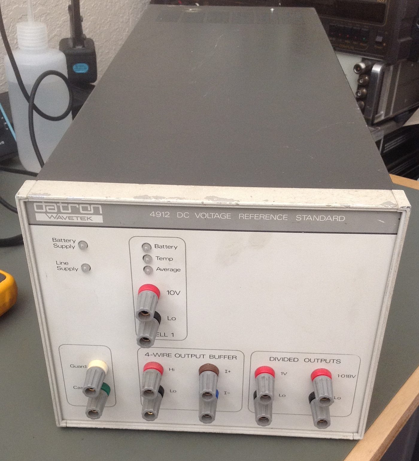
Image 113. Single-cell 4912 unit
The unit was opened and inspected for obvious issues. Apart from a cable from the battery assembly being disconnected, there was nothing that appeared wrong visually. Time for disassemble and tests.
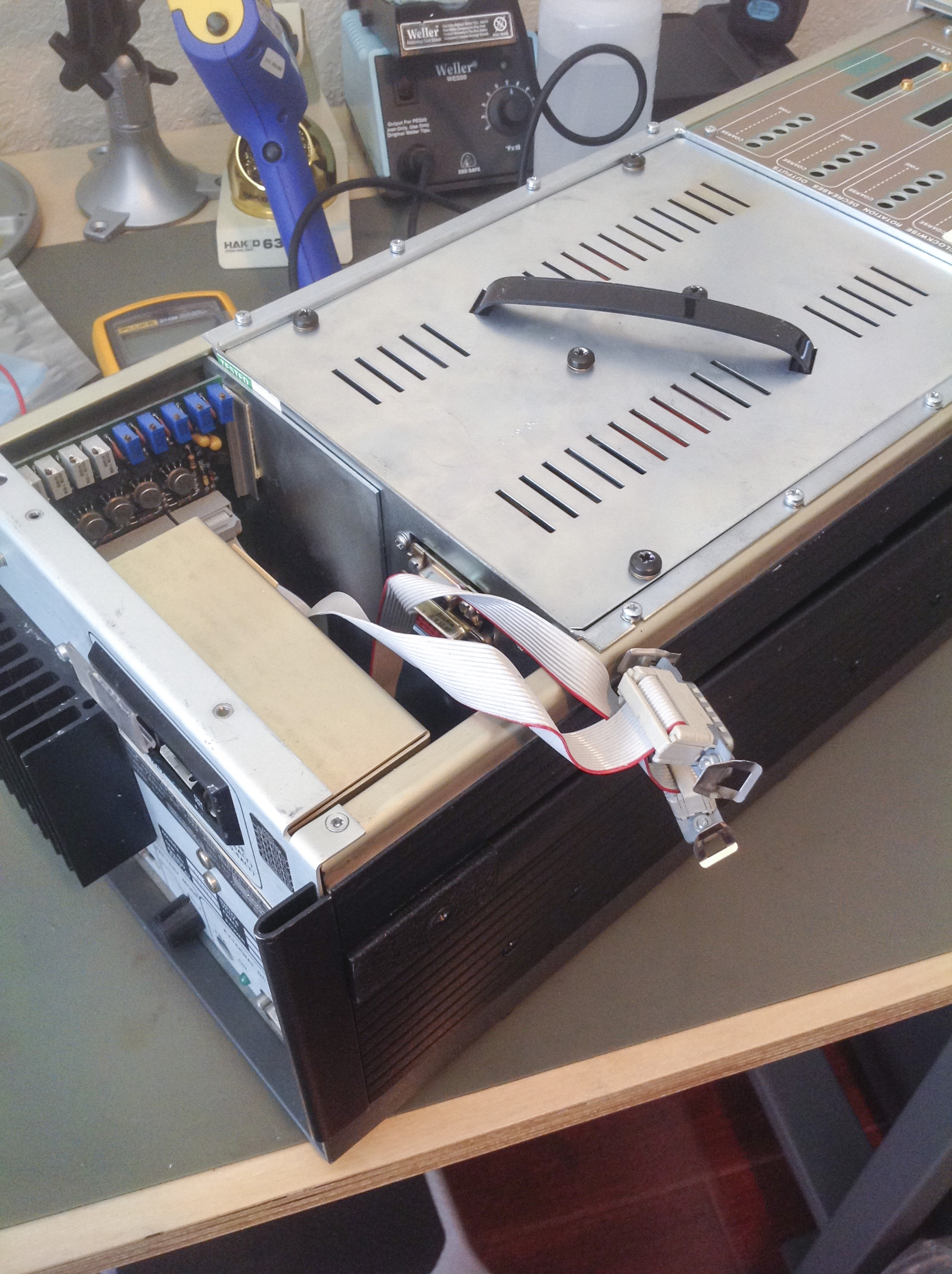
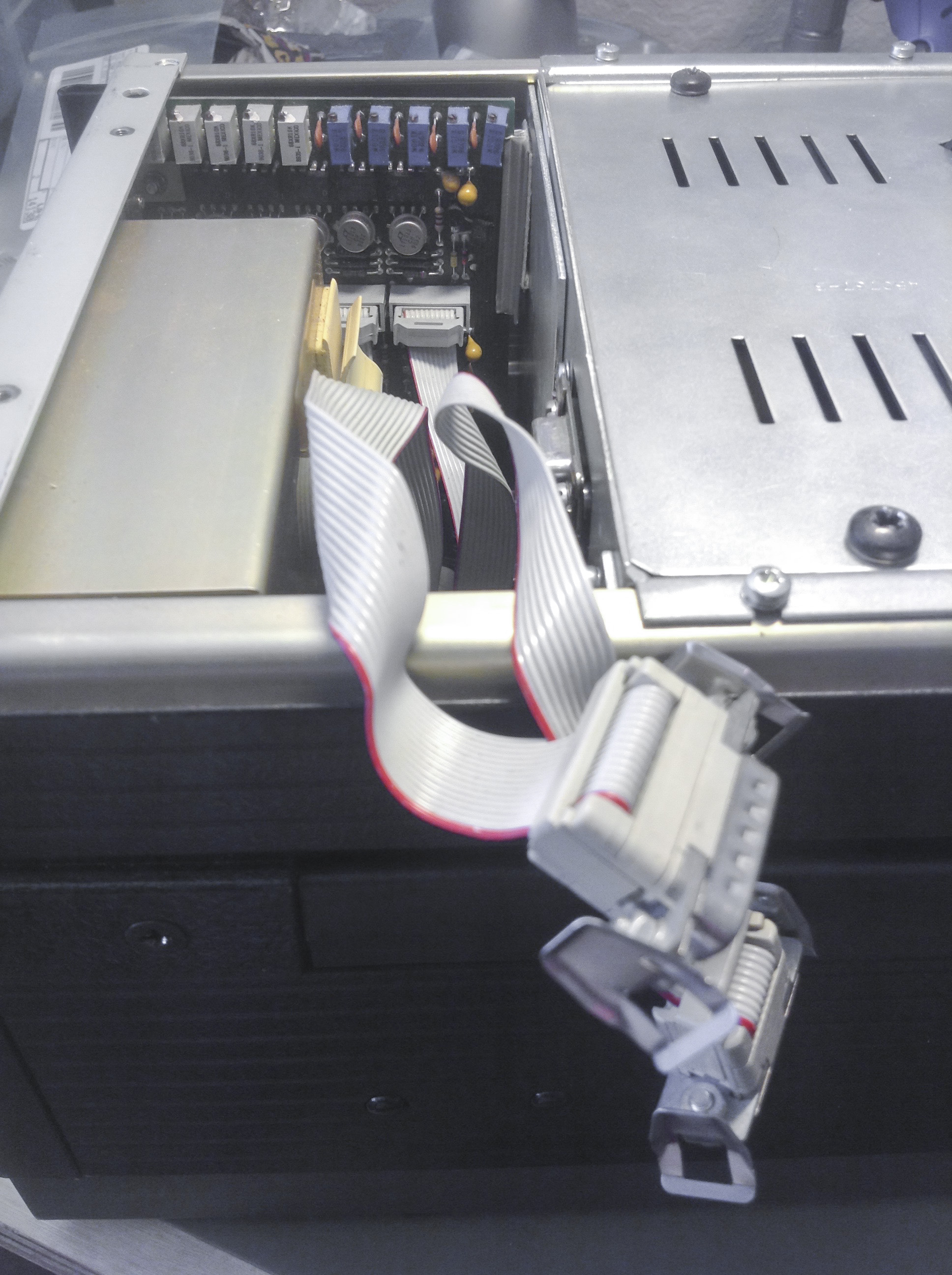
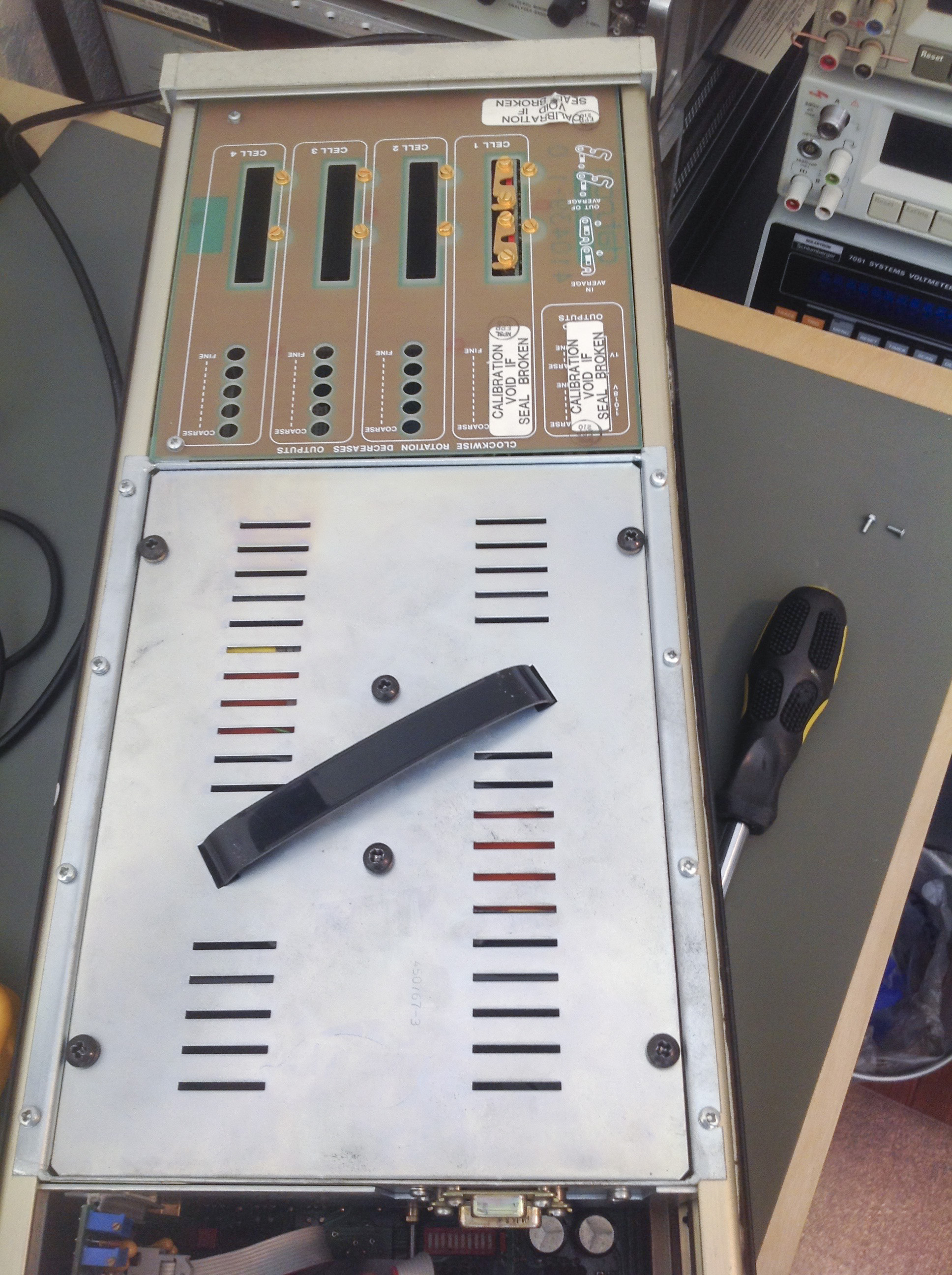
Image 114-116. Removed cover of 4912
Battery compartment:
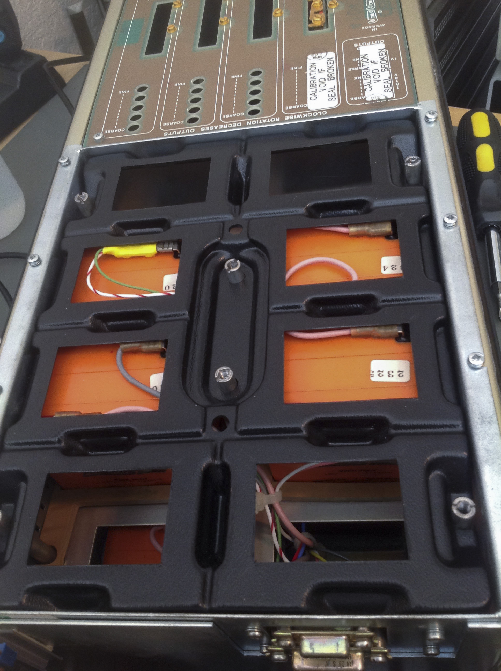
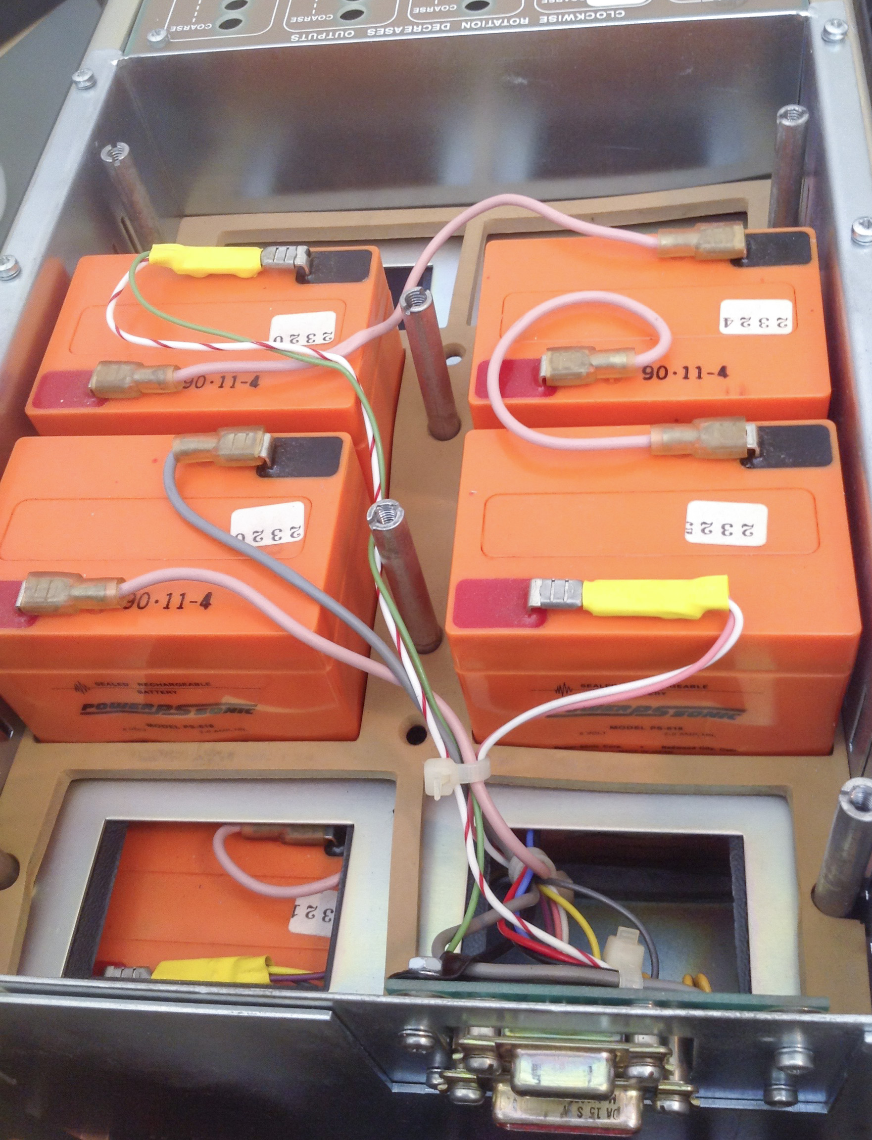
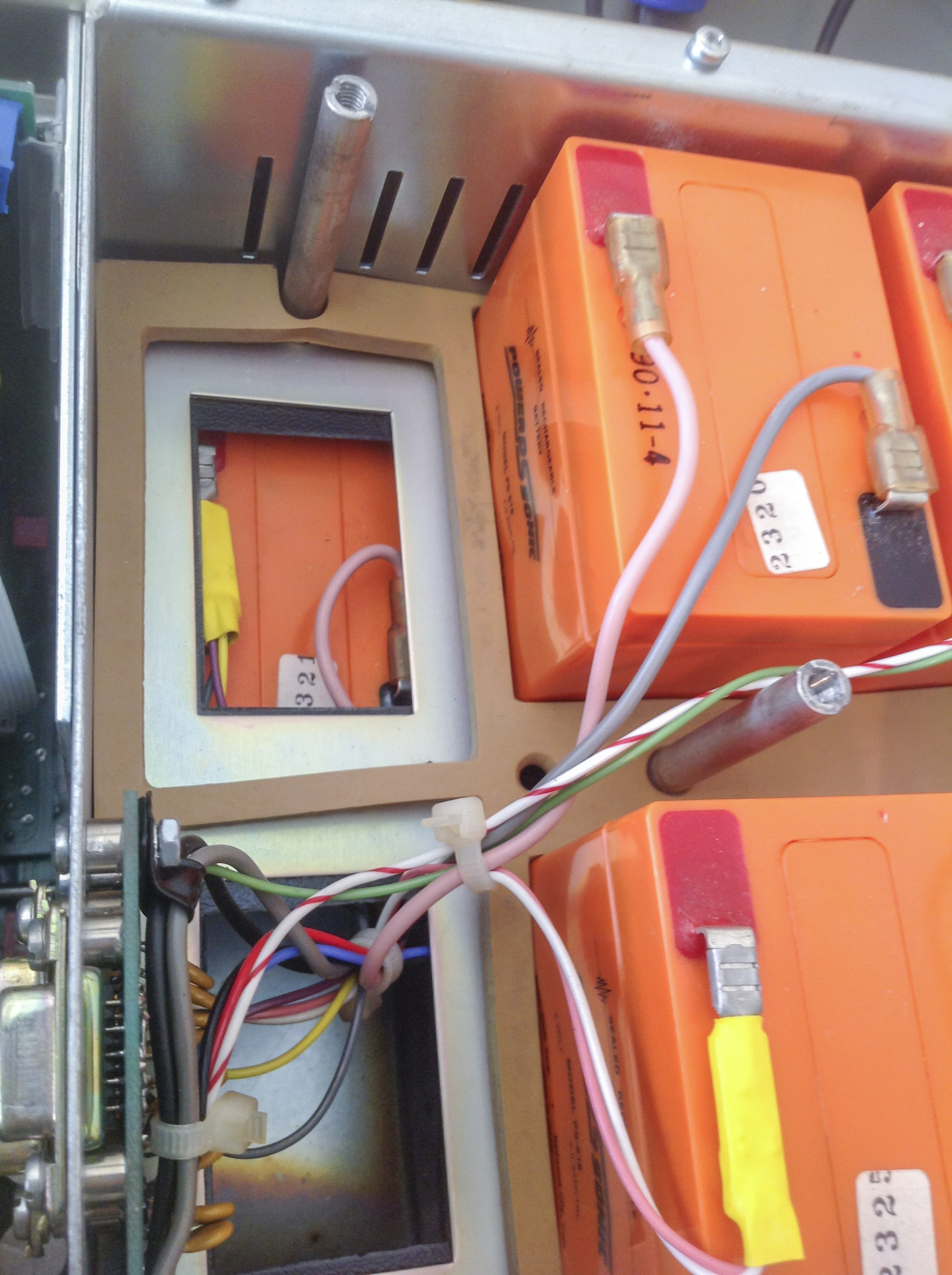
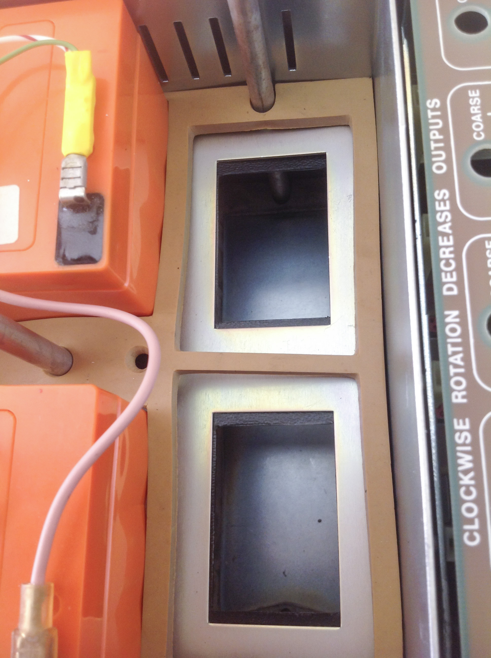
Image 117-120. Original battery compartment
Original batteries were Powersonic PS-618 rated for 6 Volt and 2.0 Amp*hour capacity. These are not available anymore and smaller replacement is PS-621 which are quite different mechanically.
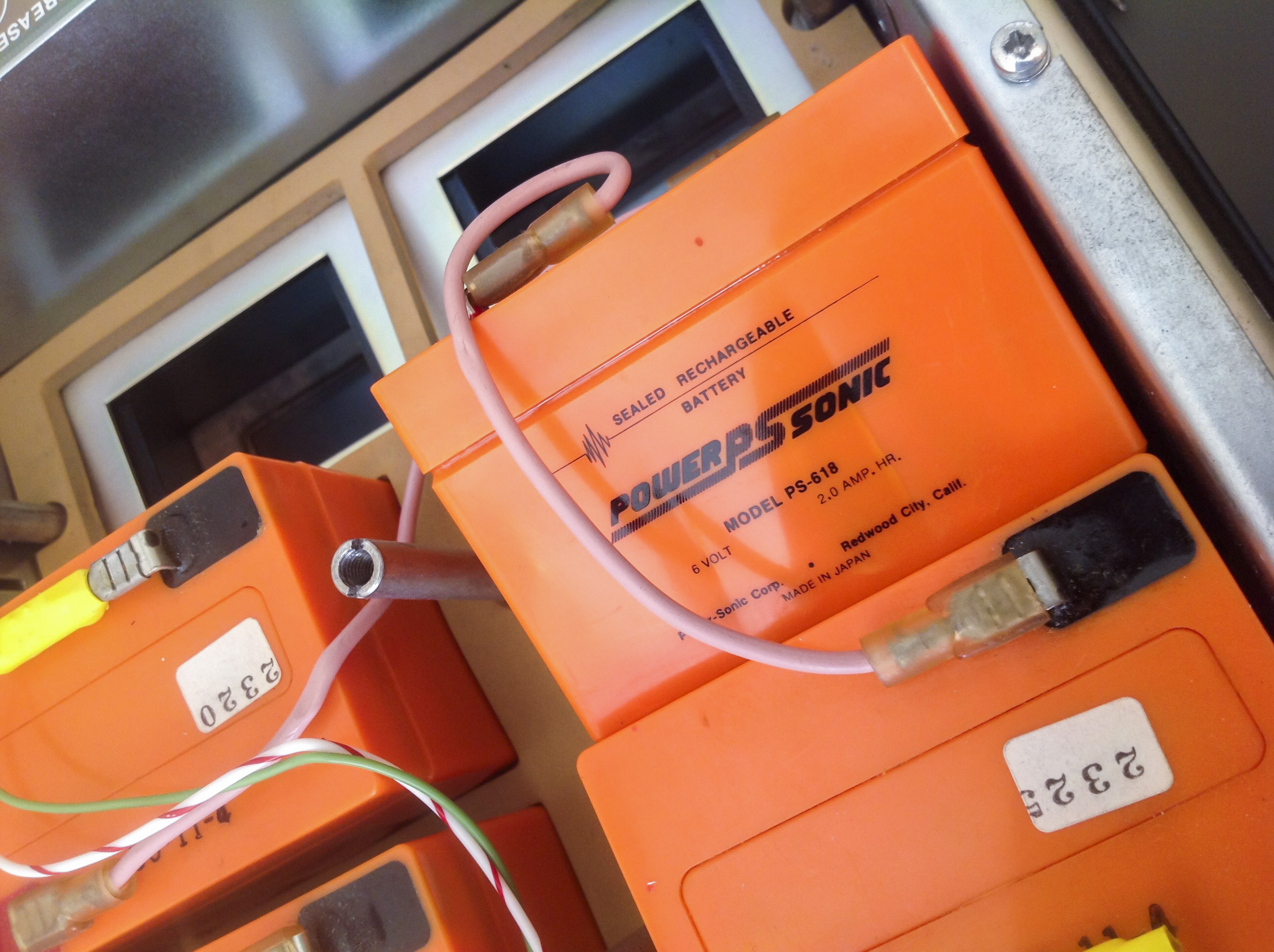
Image 121. Battery with original pack assembly, PowerSonic PS-618
Power Supply Assembly
The power supply is part of the rear cover. It includes the transformer, power supply pcb, an external DC input connector, and a power input module. The power supply pcb has five identical isolated supplies.
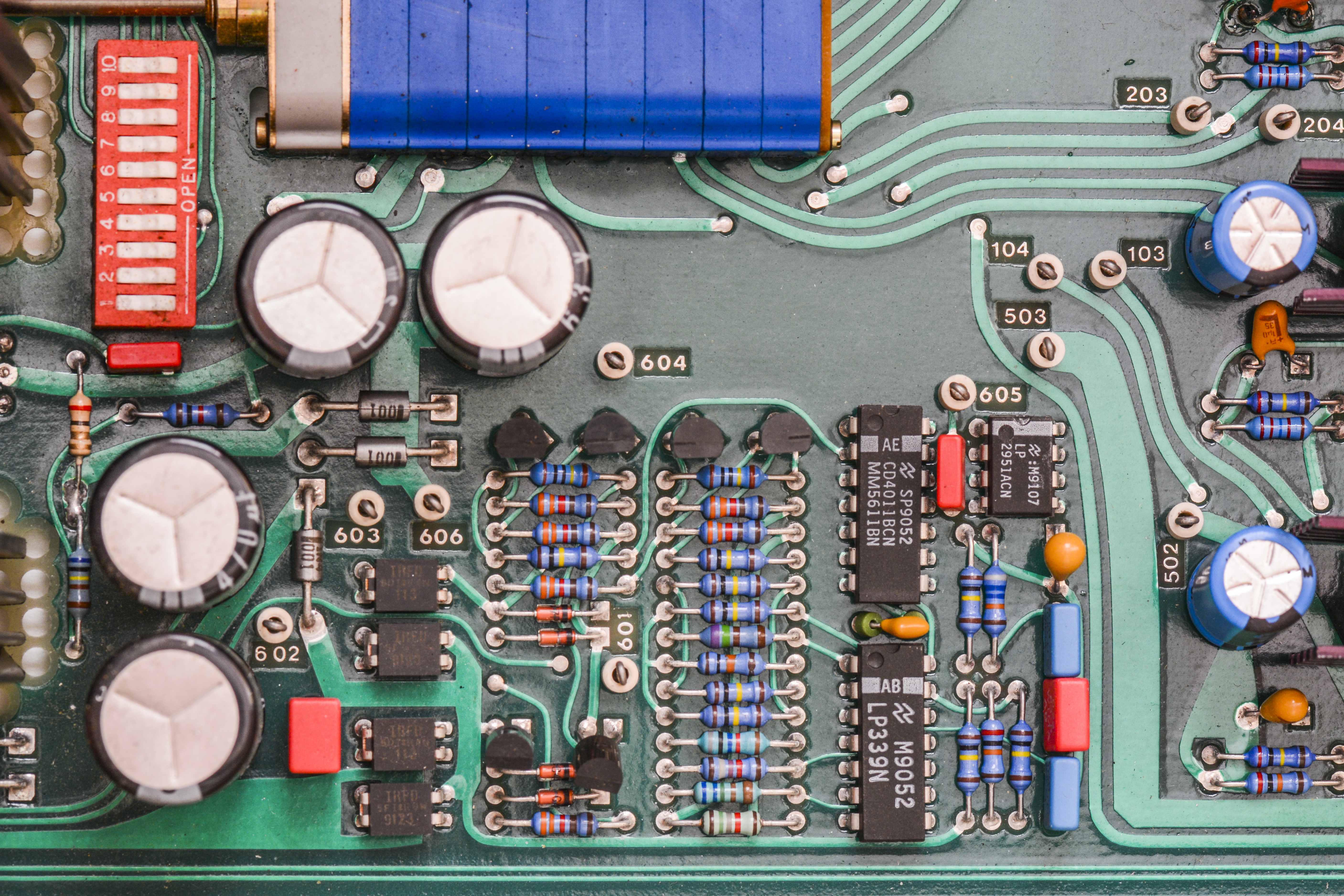
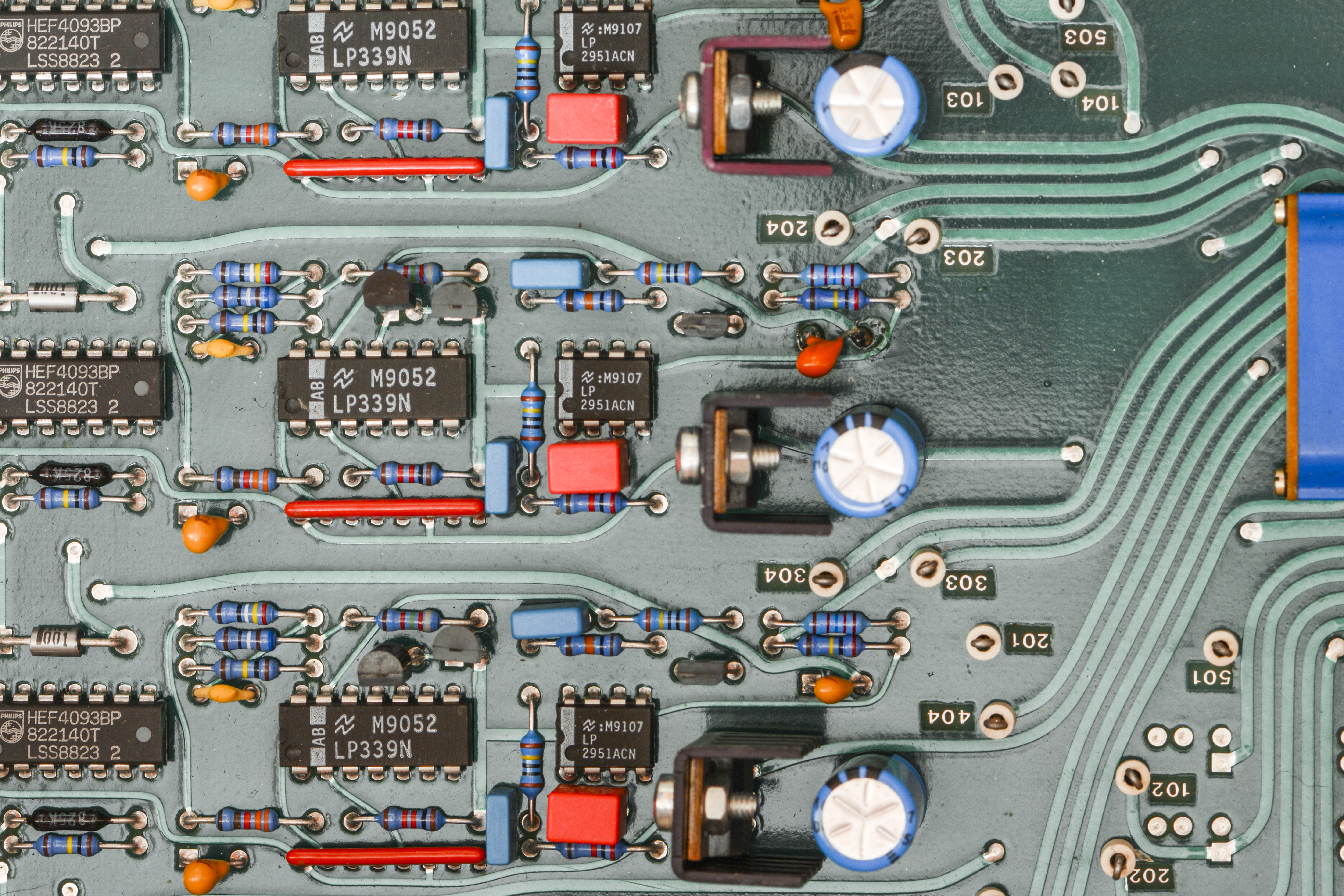
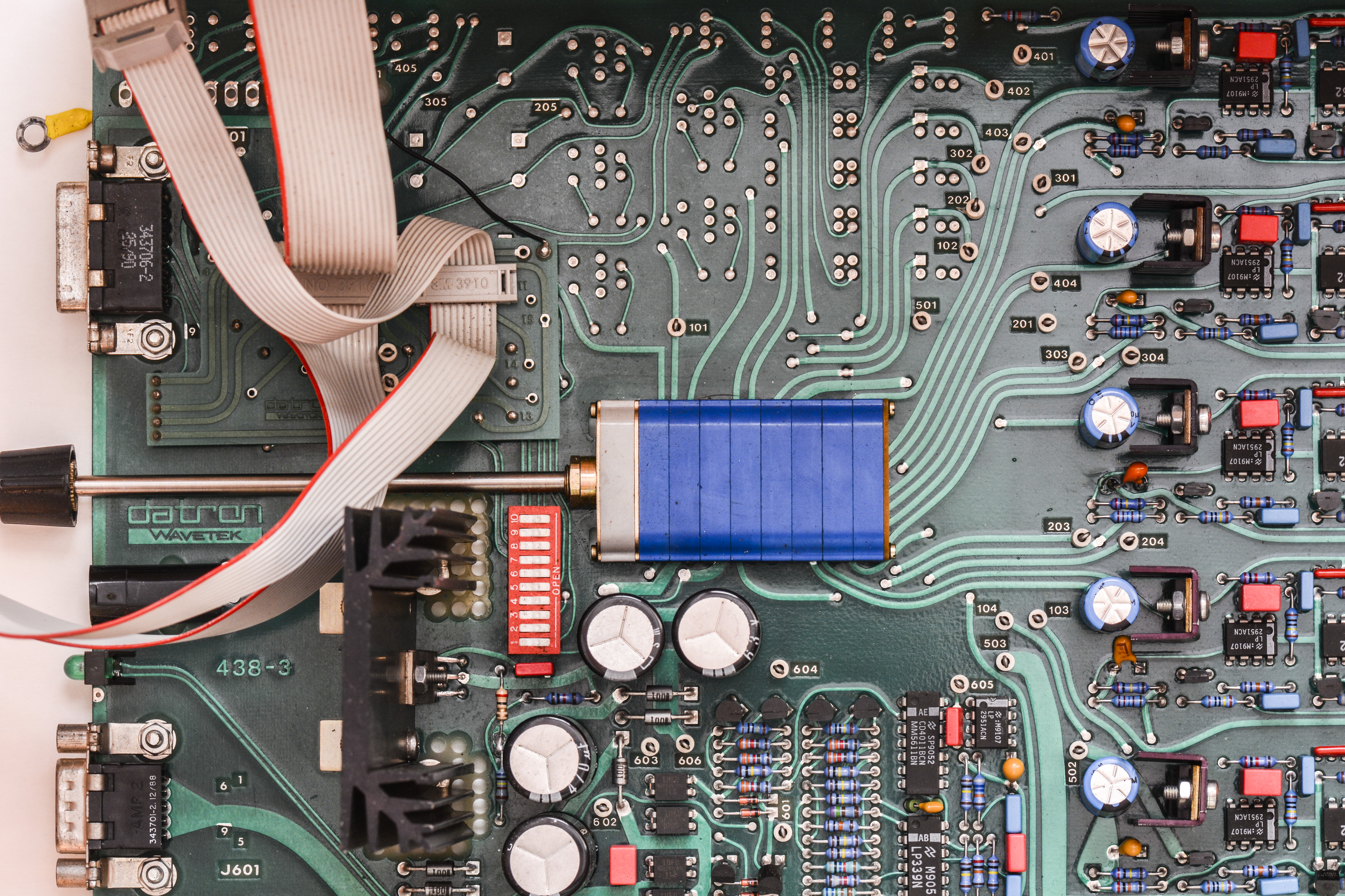
Image 122-124. Motherboard in Datron 4912
It was easier to troubleshoot by comparing outputs of each of the regulators. Two of the regulators had a low input voltage. The circuits were traced out but no issue was found with the parts on the board. It was determined that the ground path in the two circuits was interrupted. The 1N4148 diode in the path on the ground side was removed and tested to be good using a Peak DCA75 on both supplies. A diode from one of the other supplies was removed for comparison and it was discovered that it was a 10V zener. Somehow the diodes were changed and the wrong type was installed. After replacing both diodes, the two supplies sprang to life and all looked well.
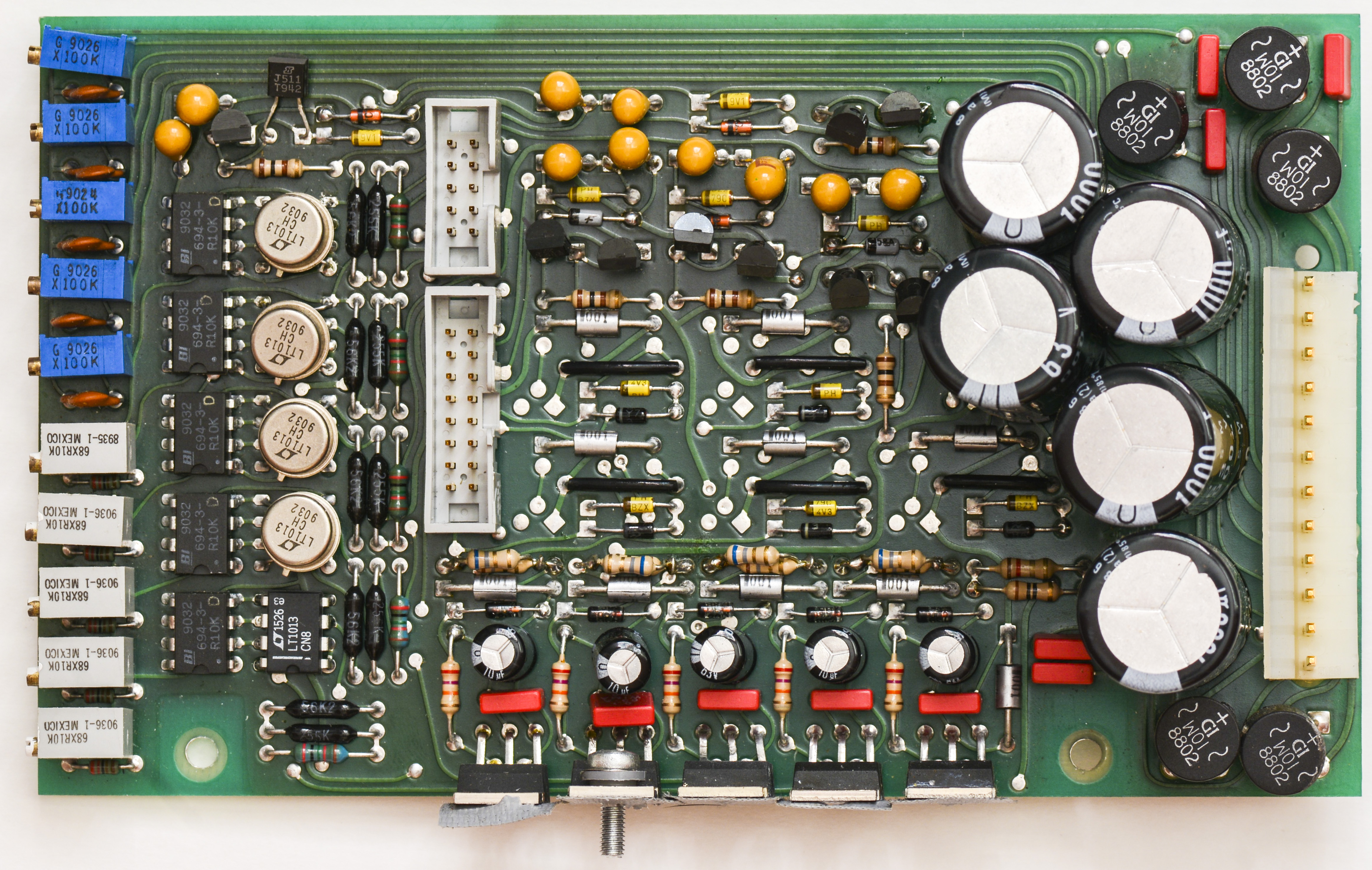
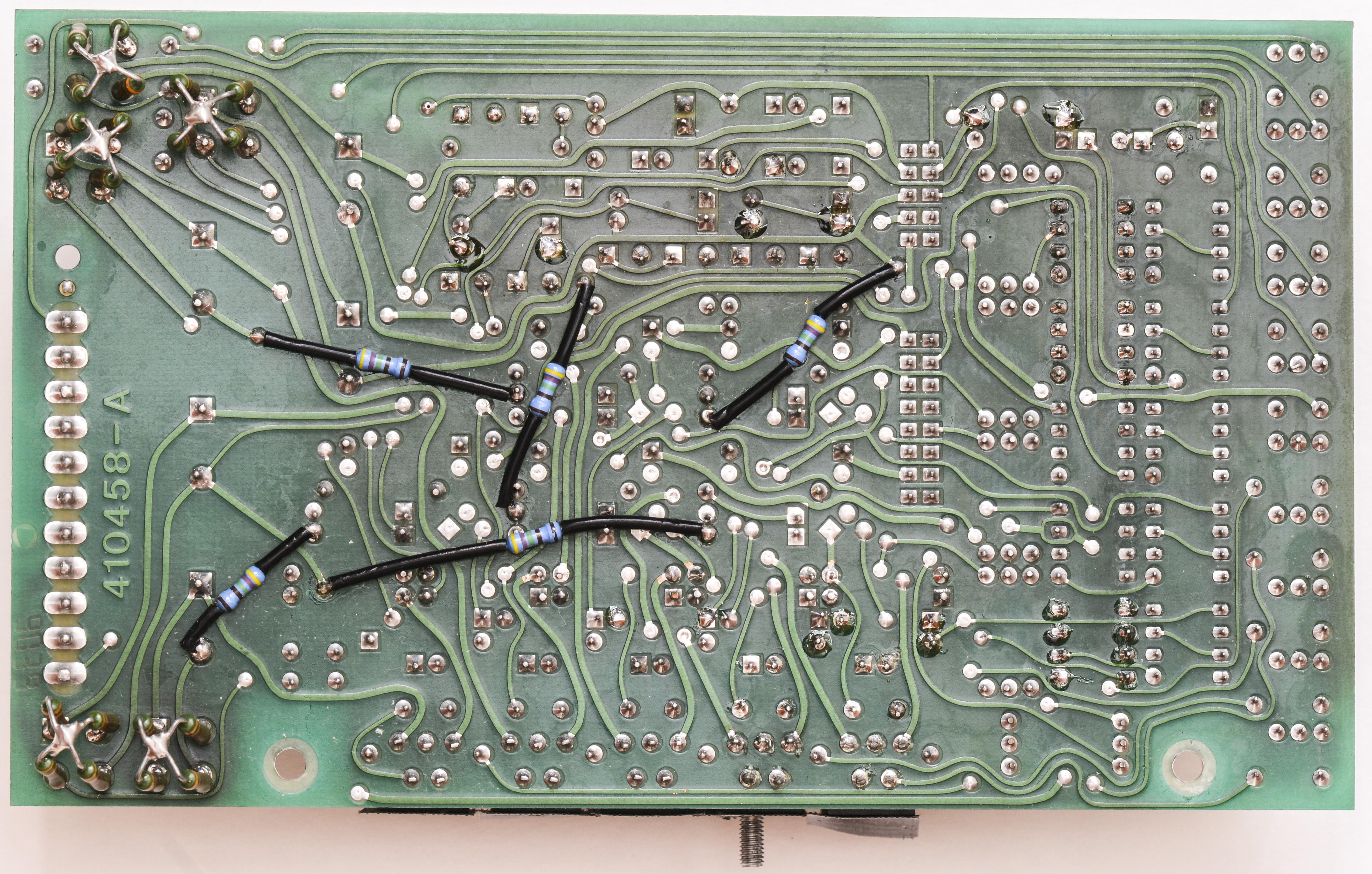
Image 125-126. Charger circuitry, same layout as in service manual
Further testing of the 10 V output still showed no change in the output level. More troubleshooting was needed.
Main Board Assembly
The main board includes separate circuits for each of the five supplies from the power supply assembly. This too made it easy to test. There is also a circuit to handle an external DC supply with its own regulator. A transit mode switch is also located on the board. The switch is used to select a low power mode for shipping of the reference. The switch protrudes from the rear cover. There are also connectors for up to four cell PCBs. It appears that Datron used the same backplane design for all three models. In the 4912 there are three slots that are not populated.
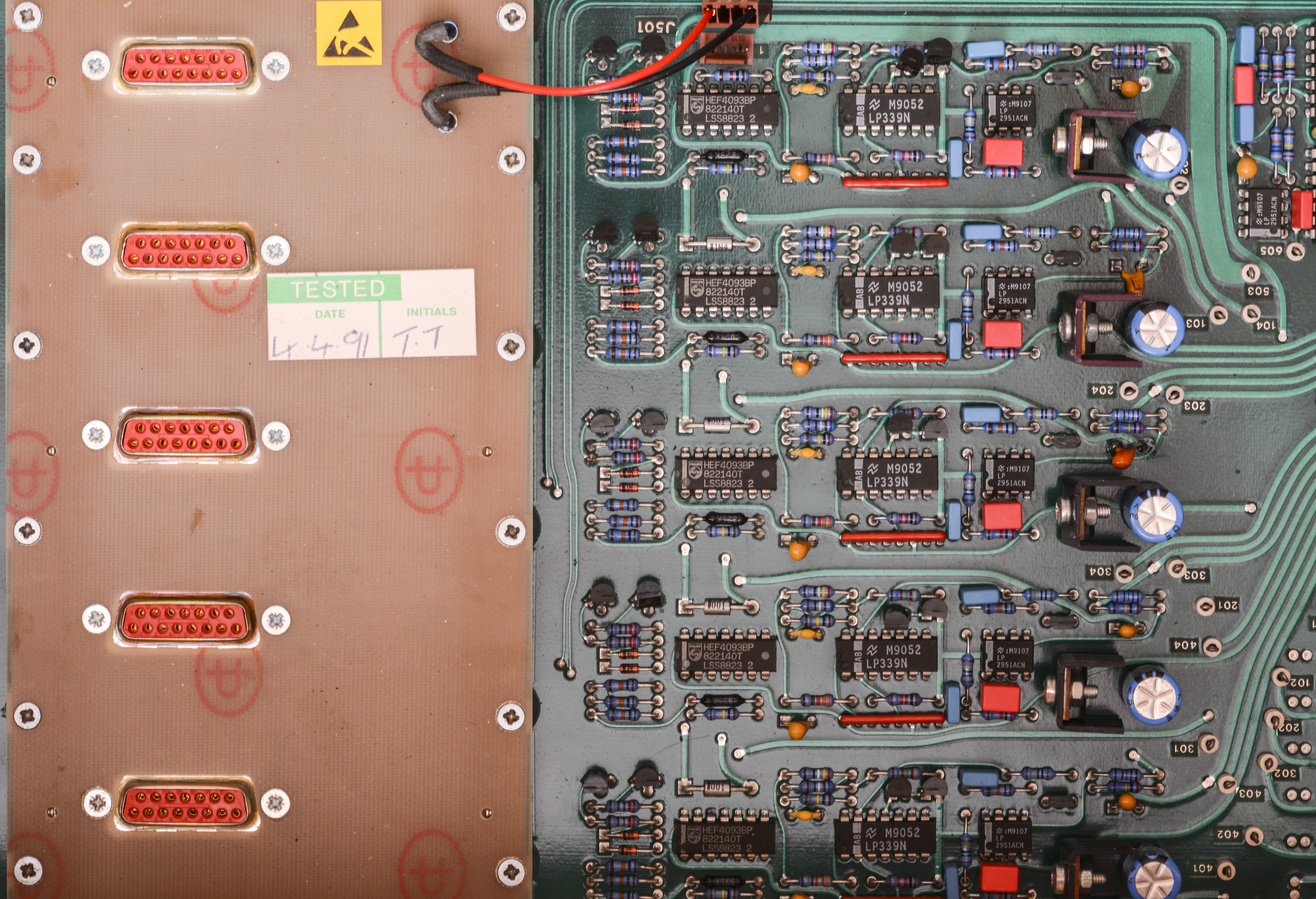
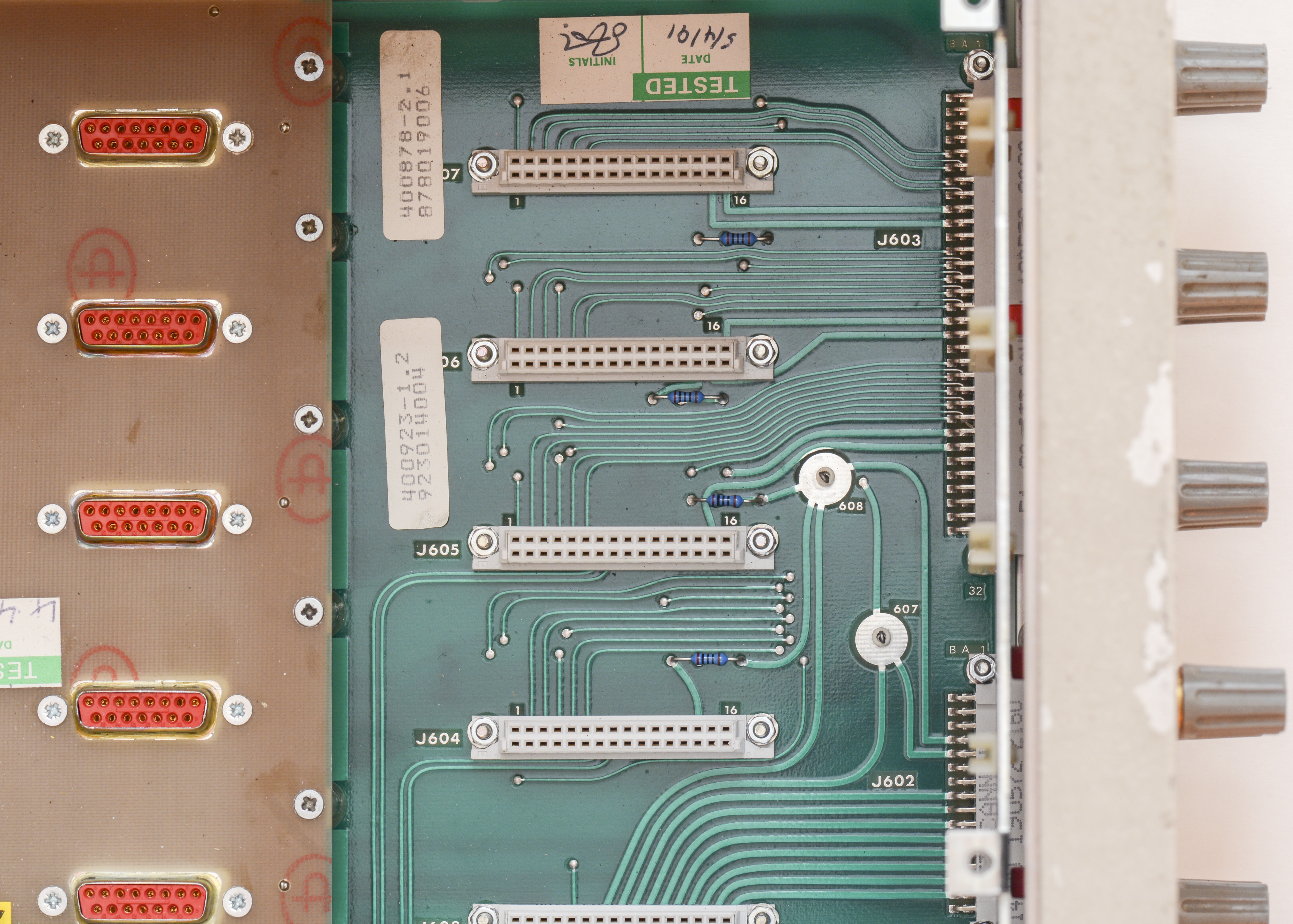
Image 127-128. Backplane interface connectors for cards
Comparing the voltages on each of the five circuits, it was found that the 12V was missing from two of three unused supplies. They have probably been defective for a long time but they had no effect on the operation of the single cell. The two supplies still needed to be repaired. The inputs were tested and found to be low. Measuring the resistance across the input path found that the two inputs were shorted to their respective grounds.
There is a 1µF/35V tantalum on the inputs. They were removed and confirmed to be shorted. A temporary replacement was installed and the supplies were retested as having good outputs. Again, the reference output was tested but the output was still at 0.5 V. Off to the cell PCB…
Cell PCB Assembly
The cell pcb contains the LTZ1000 daughterboard assembly and also the PWM divider circuits. The divider is broken into a most significant switch and a least significant switch of 16-bits and 8-bits.

Image 129. Reference module installed for Cell A
The output of the LTZ board measured at ~7.23V between TP105 and TP108. This meant the problem was most likely in the output divider or op-amps. The HI and LO side of the output splits into both the direct output and averaged output. The continuity between the LTZ board LO out and the front panel LO was confirmed as good. The two jumpers connecting the averaged outputs were disconnected for testing purposes.
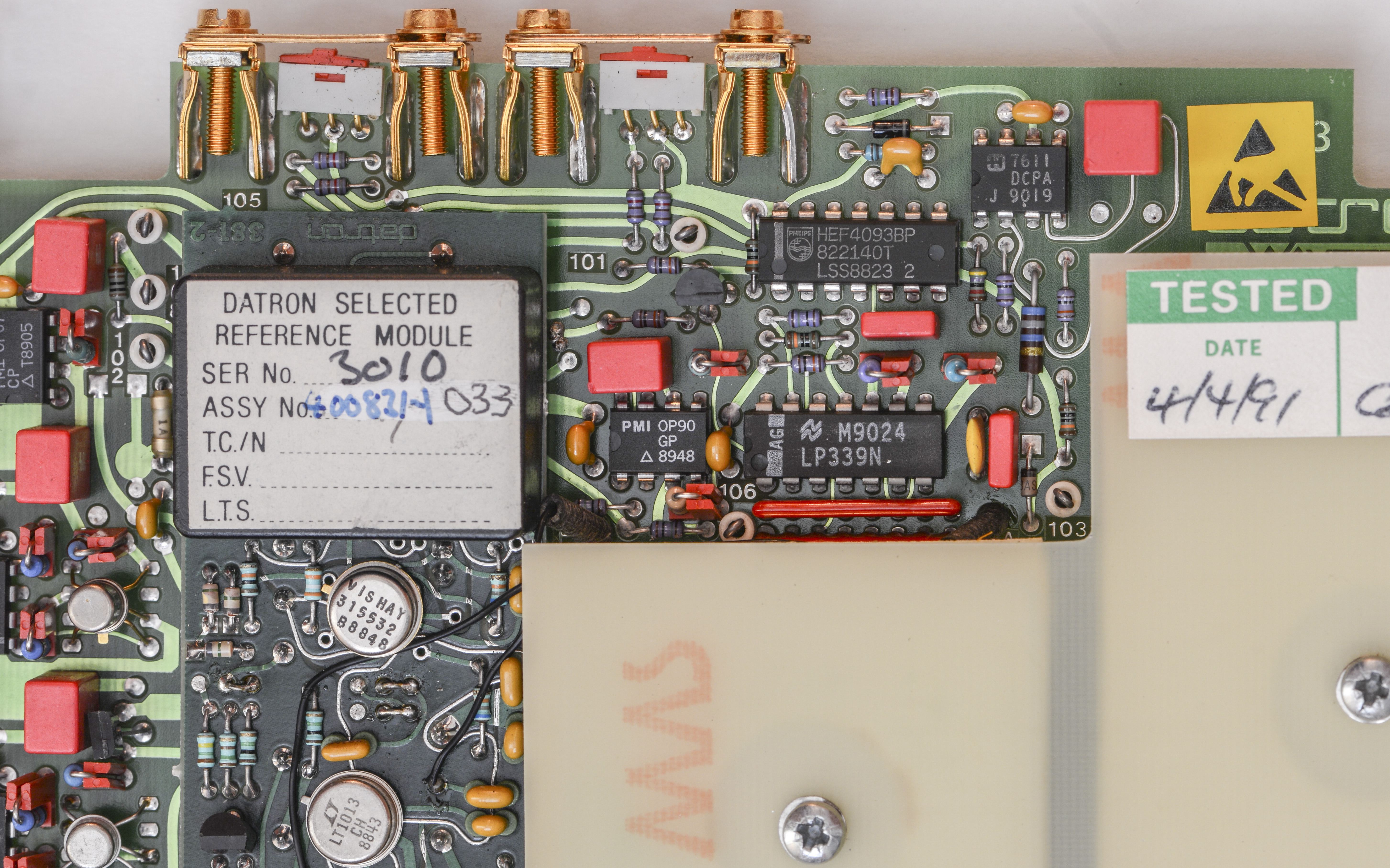
Image 130. Reference PCBA, Part Number 400821-1
The LTZ board HI side output goes through two separate op-amps. It was difficult to confirm whether U109 was working as its output was low (0.5V). U111’s output was ~11.5V but the output at the front panel was missing. The resistance between the HI and LO outputs at the front panel measured 7 ohms. It was suspected that more bad capacitors would be found.
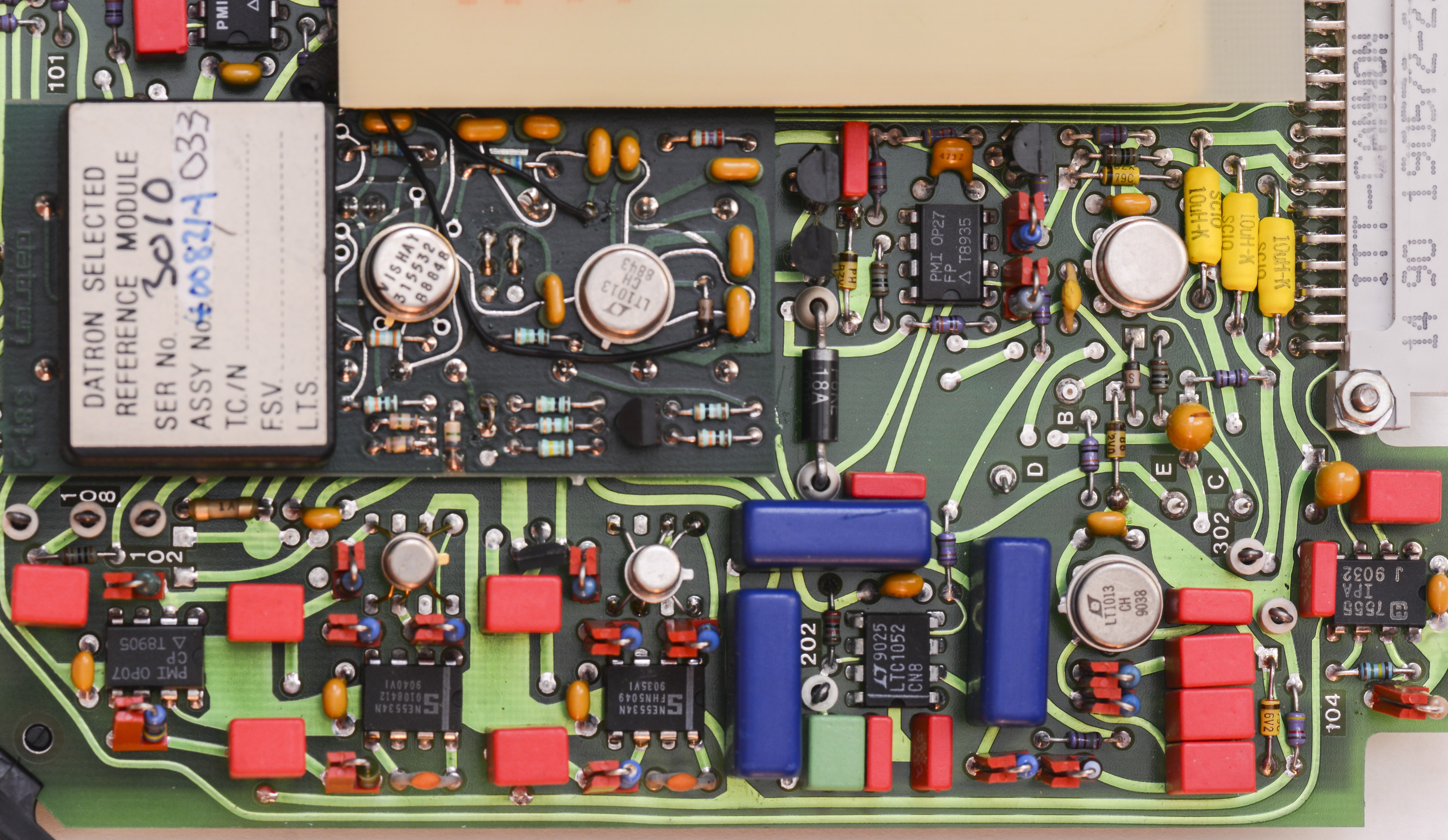
Image 131. Reference circuits
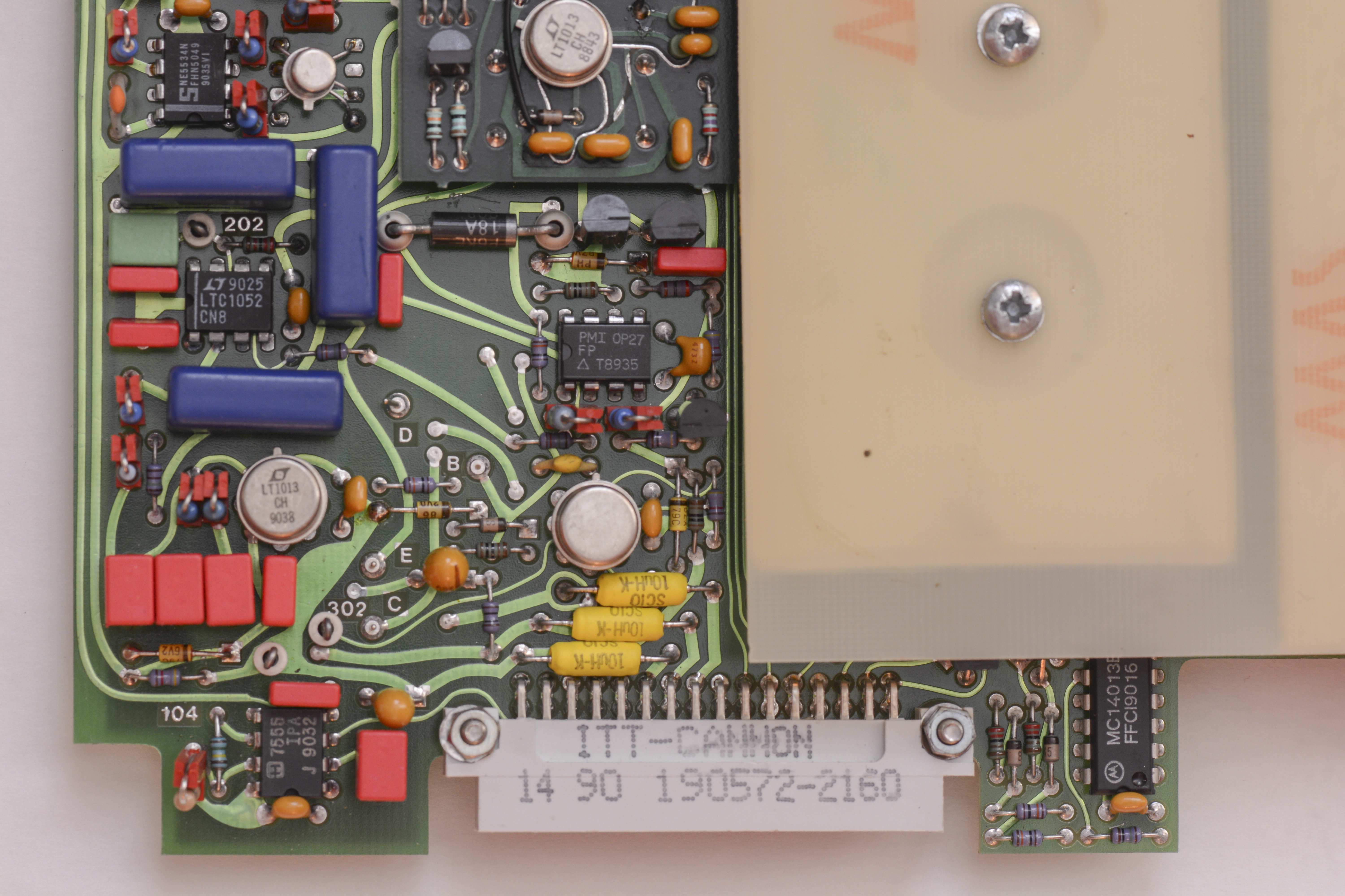
Image 132. ITT Cannon interconnect port
All capacitors on the board were measured in circuit but only a couple were across the HI/LO outputs. They were removed and measured. Neither were found to be shorted. Probing around the board searching for shorts proved nothing. The 10V path goes into both dividers. The signal name is 10V(B) according to the schematics.
All components in the two dividers were checked but the only issues found were two JFETs (Q204,Q206) had a low resistance across their terminals. They were removed from the pcb one at a time and tested on the DCA75. No readings appeared to be bad. Measuring resistance at the outputs showed that it was now ~130 ohms. The 10V output was then measured with the two transistors removed and it read 9.4V.
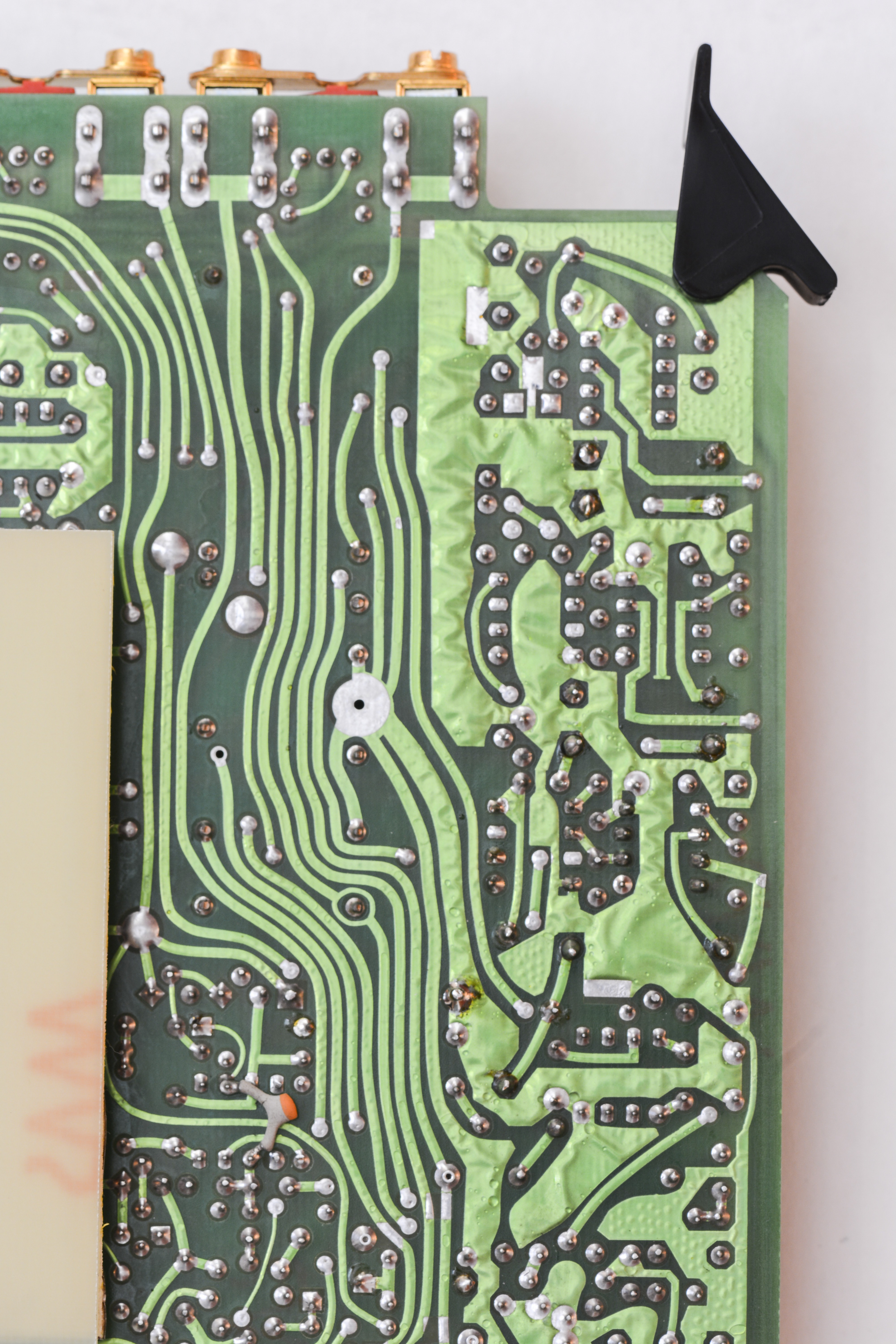
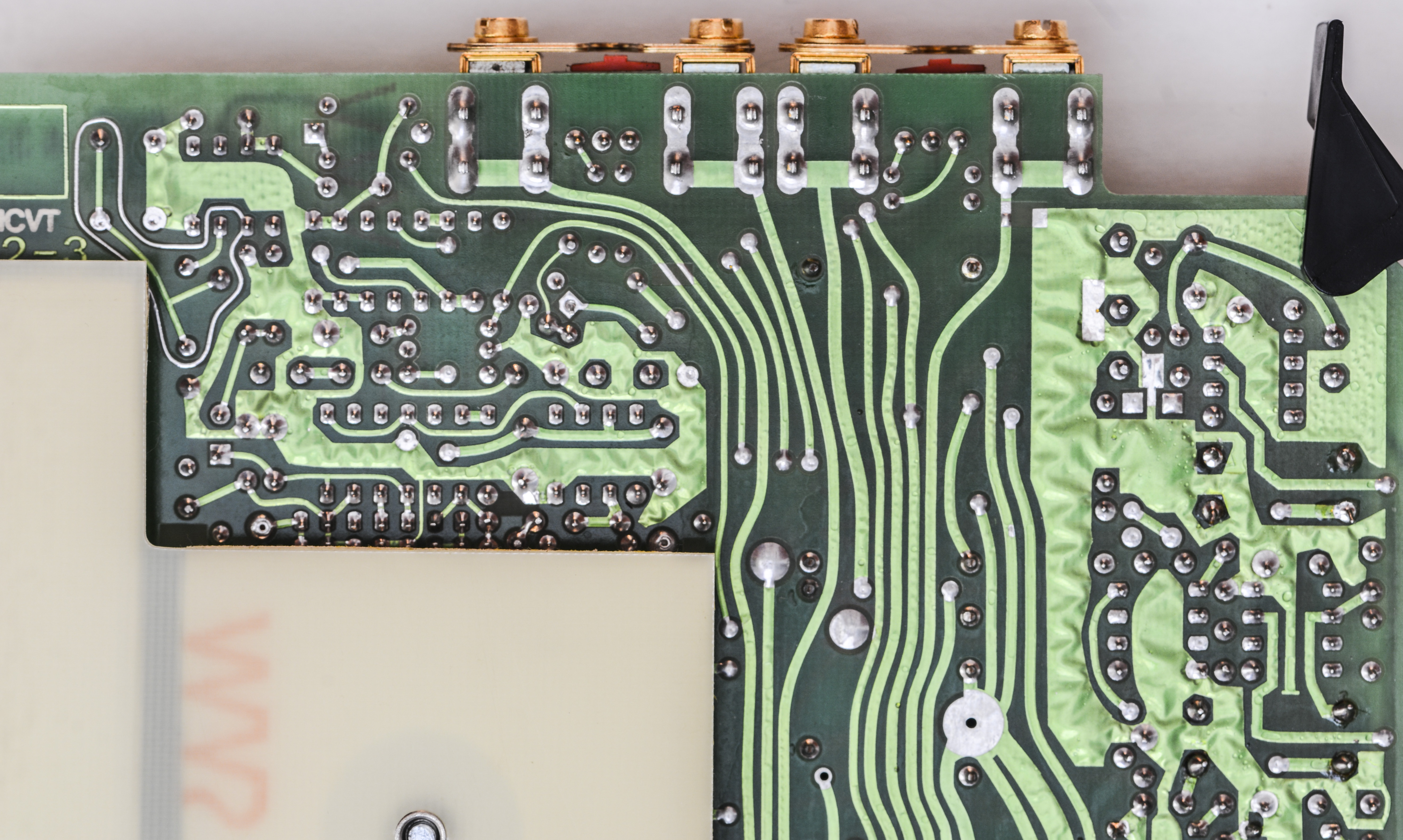
Image 133-135. Back side of the reference PCBA
Q203,Q205, and Q208 were removed and tested with the DCA75. They also tested as good. It was decided that the transistors in this part of the board would be ordered. Q204 and Q206 have been marked by Datron so most likely they are binned parts. They could also be matched to each other. This will have to be tested if either one is determined to be defective.
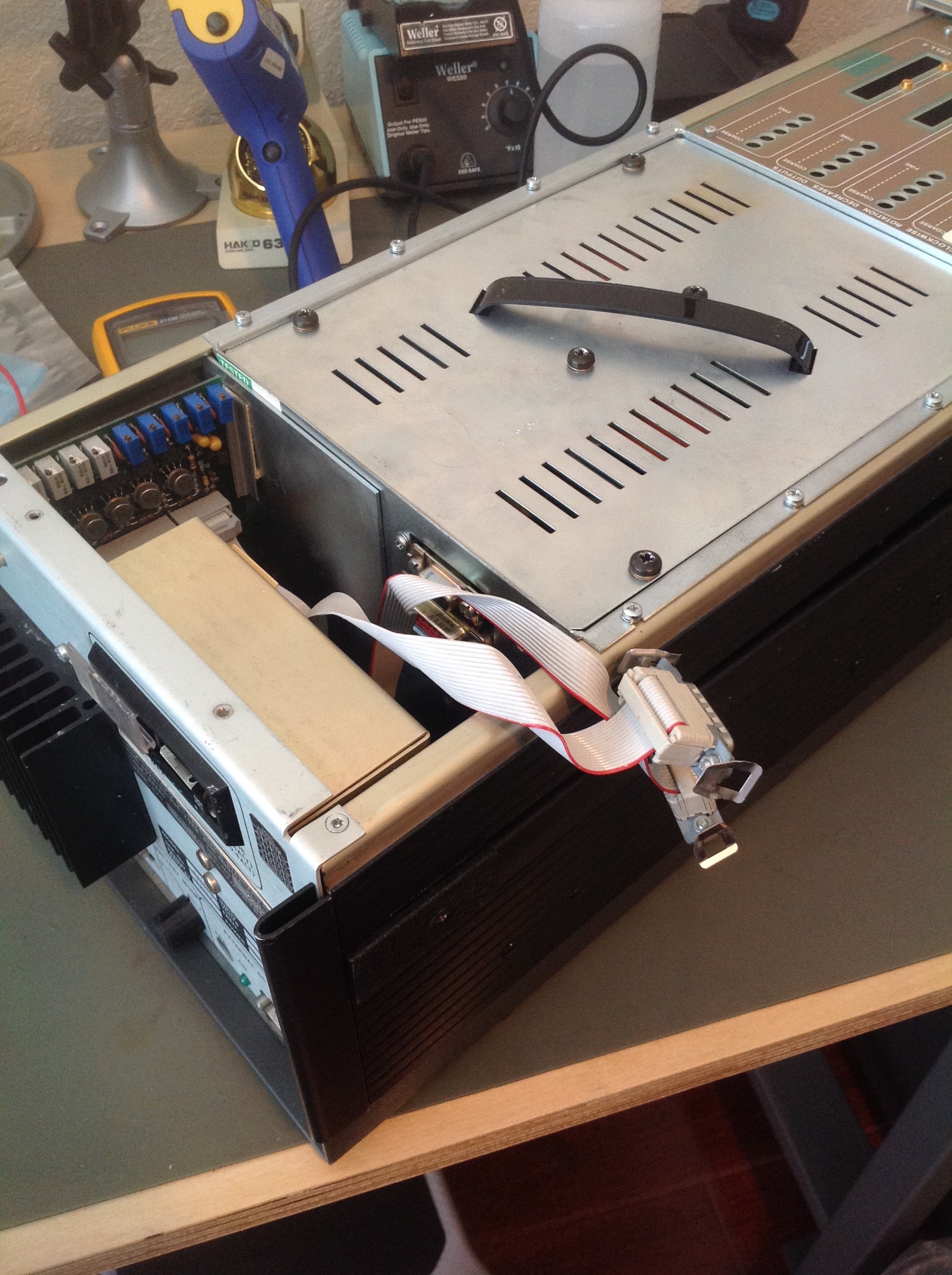
Image 136. Disconnected battery DSub ports
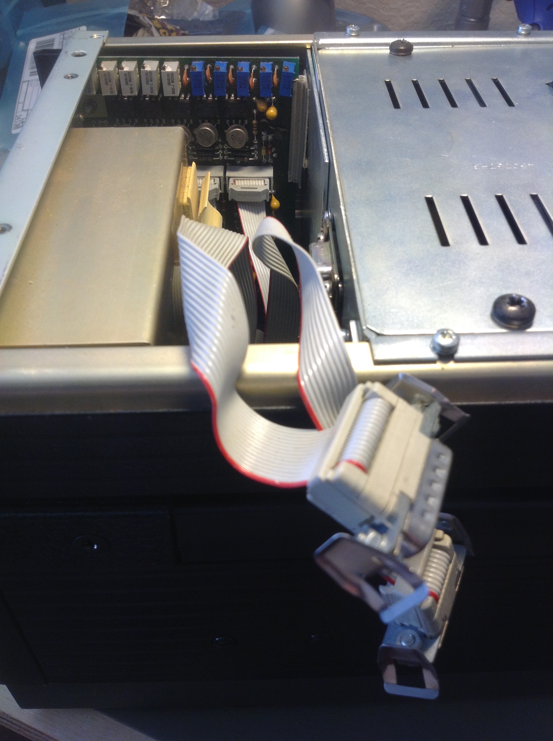
Image 137. Battery pack connections
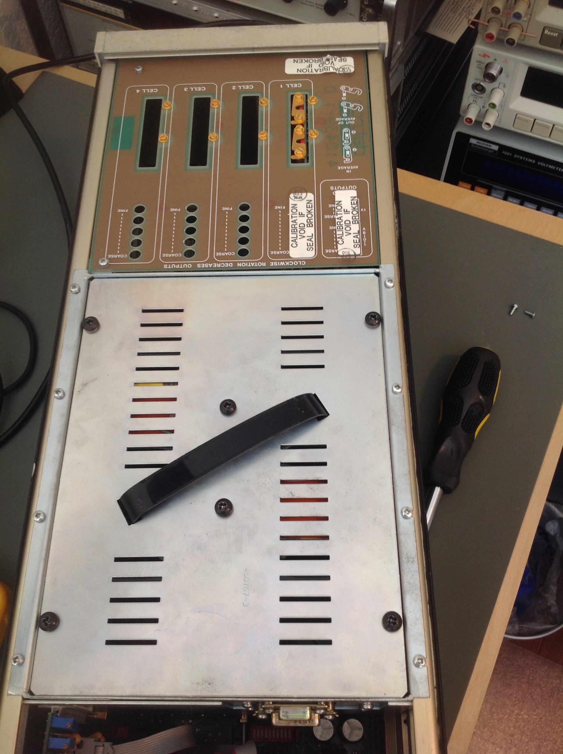
Image 138. Overlook after external cover removed
Image 139. Battery box prior to removal from the chassis
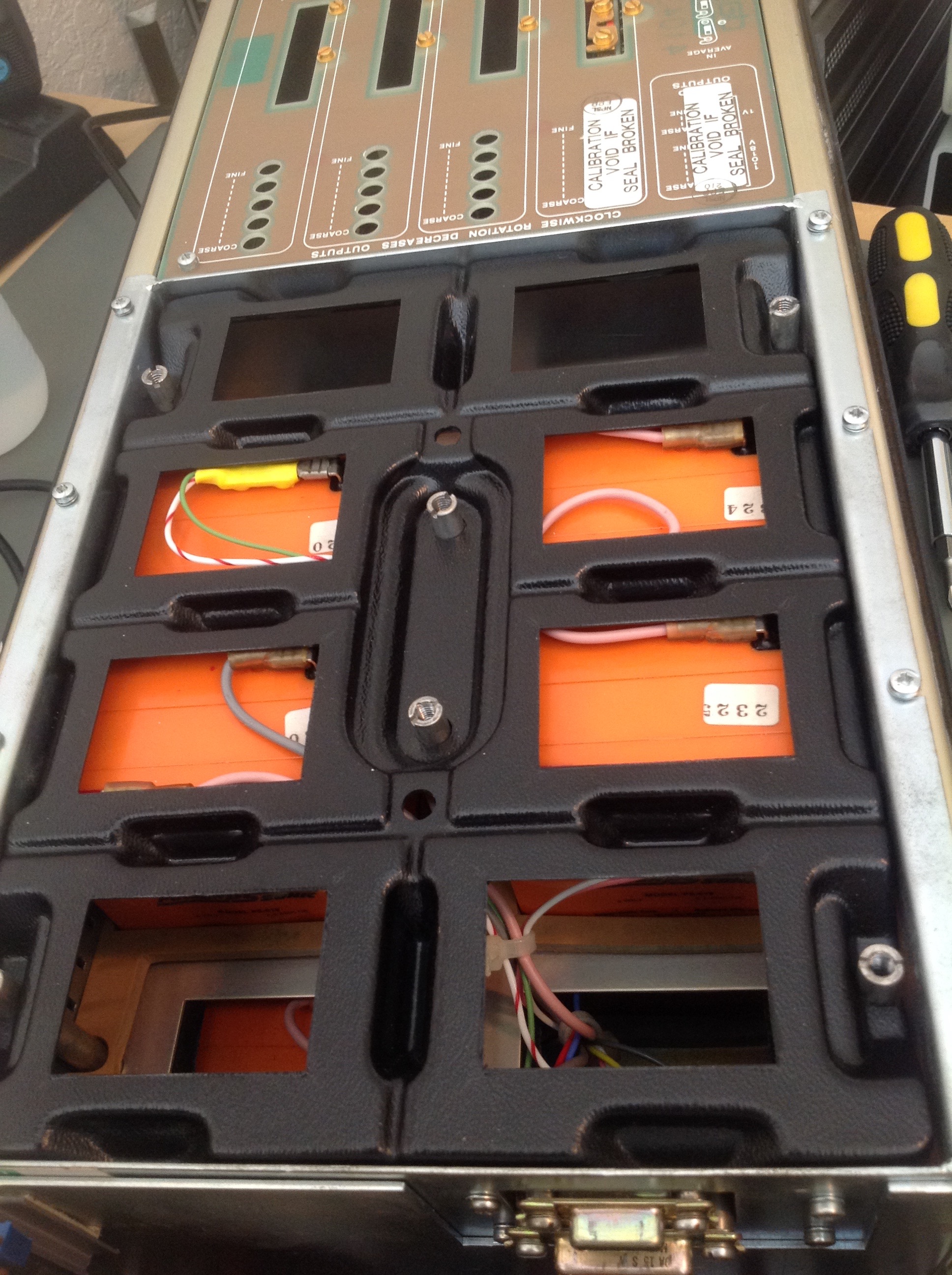
Image 140. Plastic cover spacer
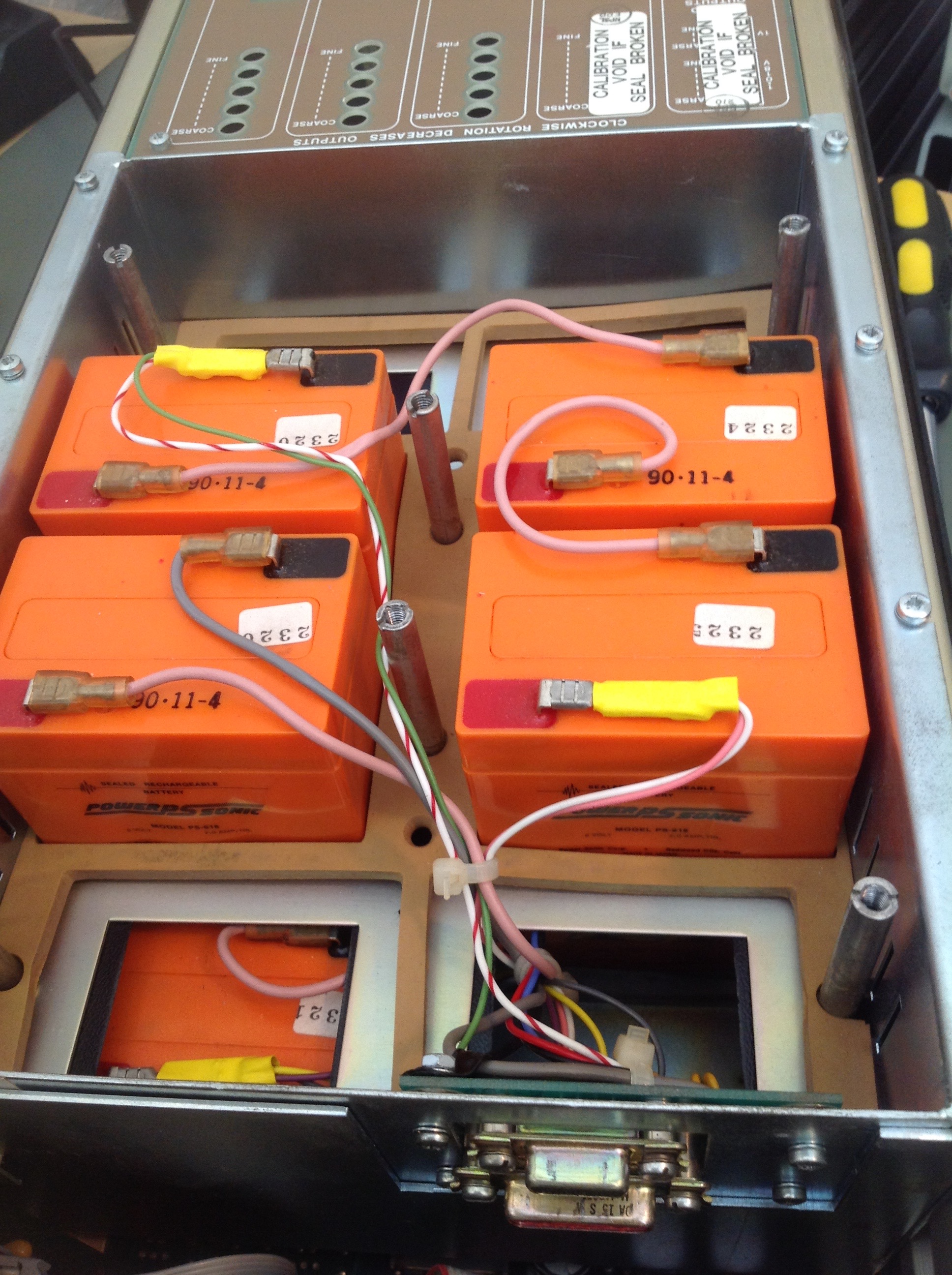
Image 141. Cell links
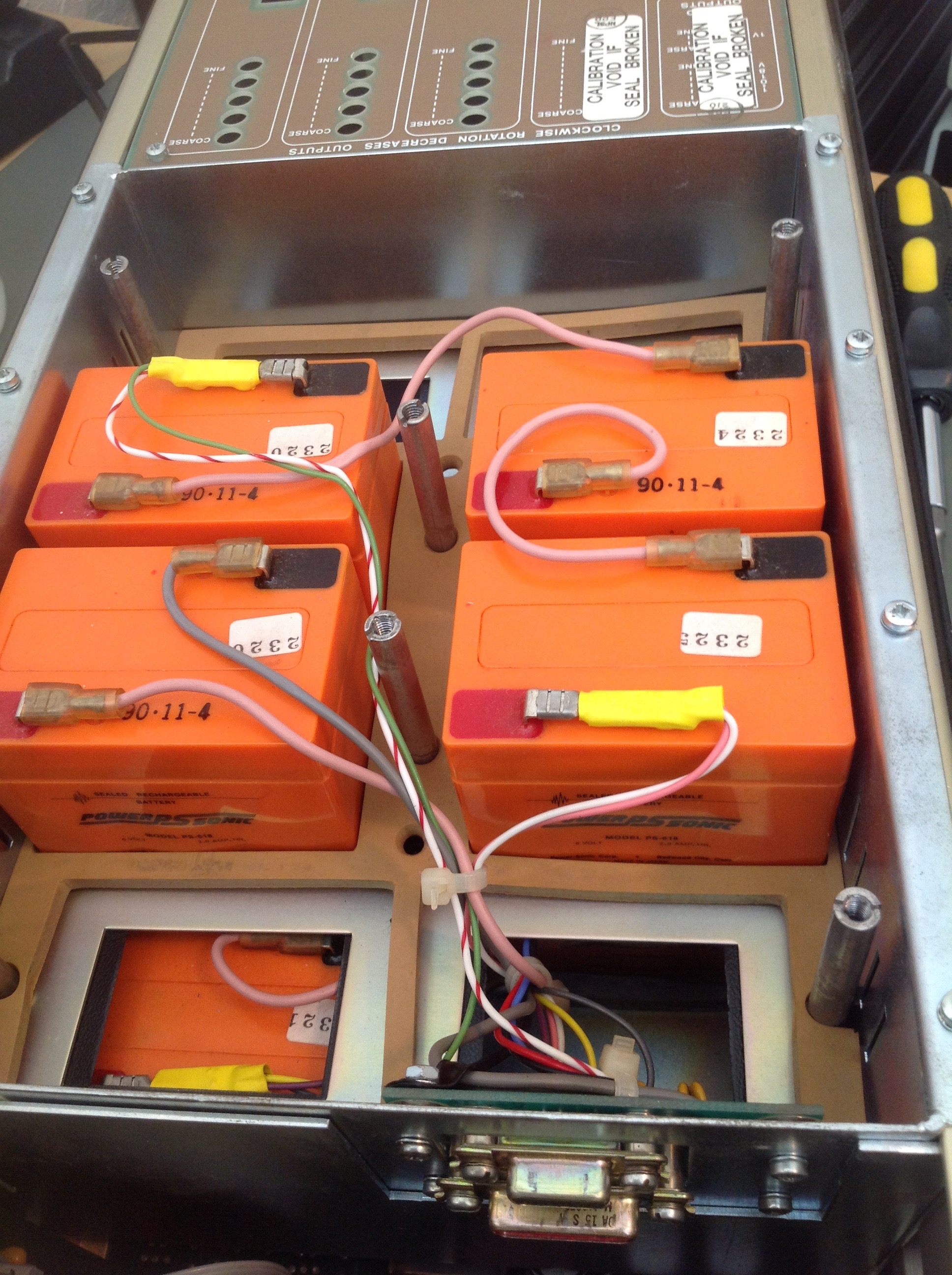
Image 142. Cell links
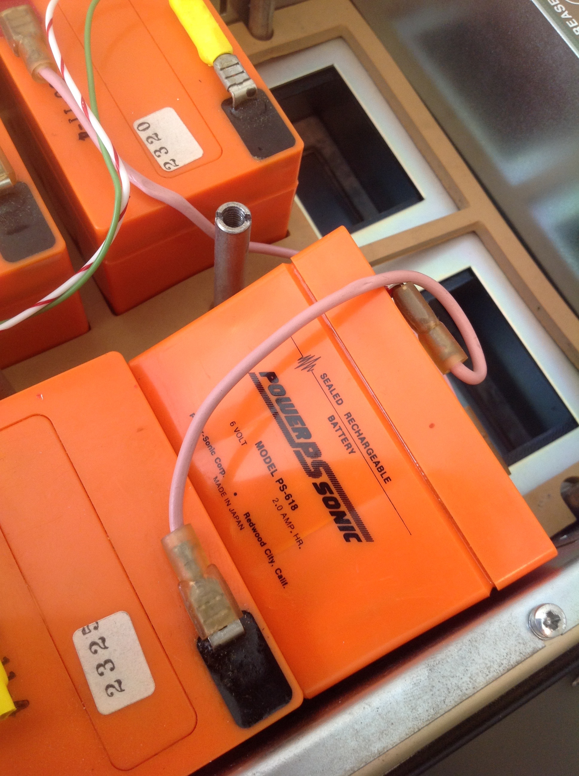
Image 143. Cell links
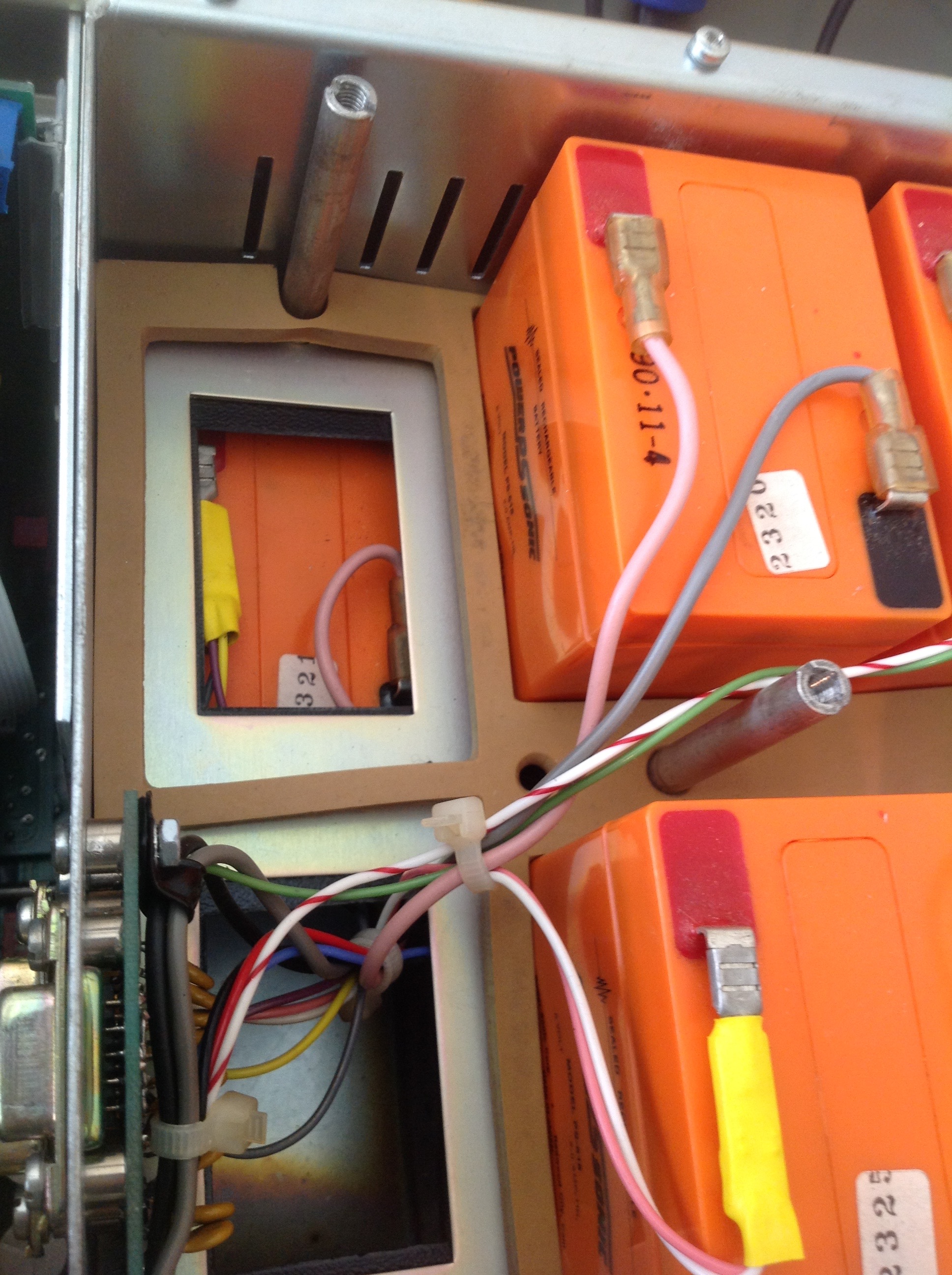
Image 144. Battery wiring from connector/fuse PCBA
Image 145. Space for battery with old battery still installed
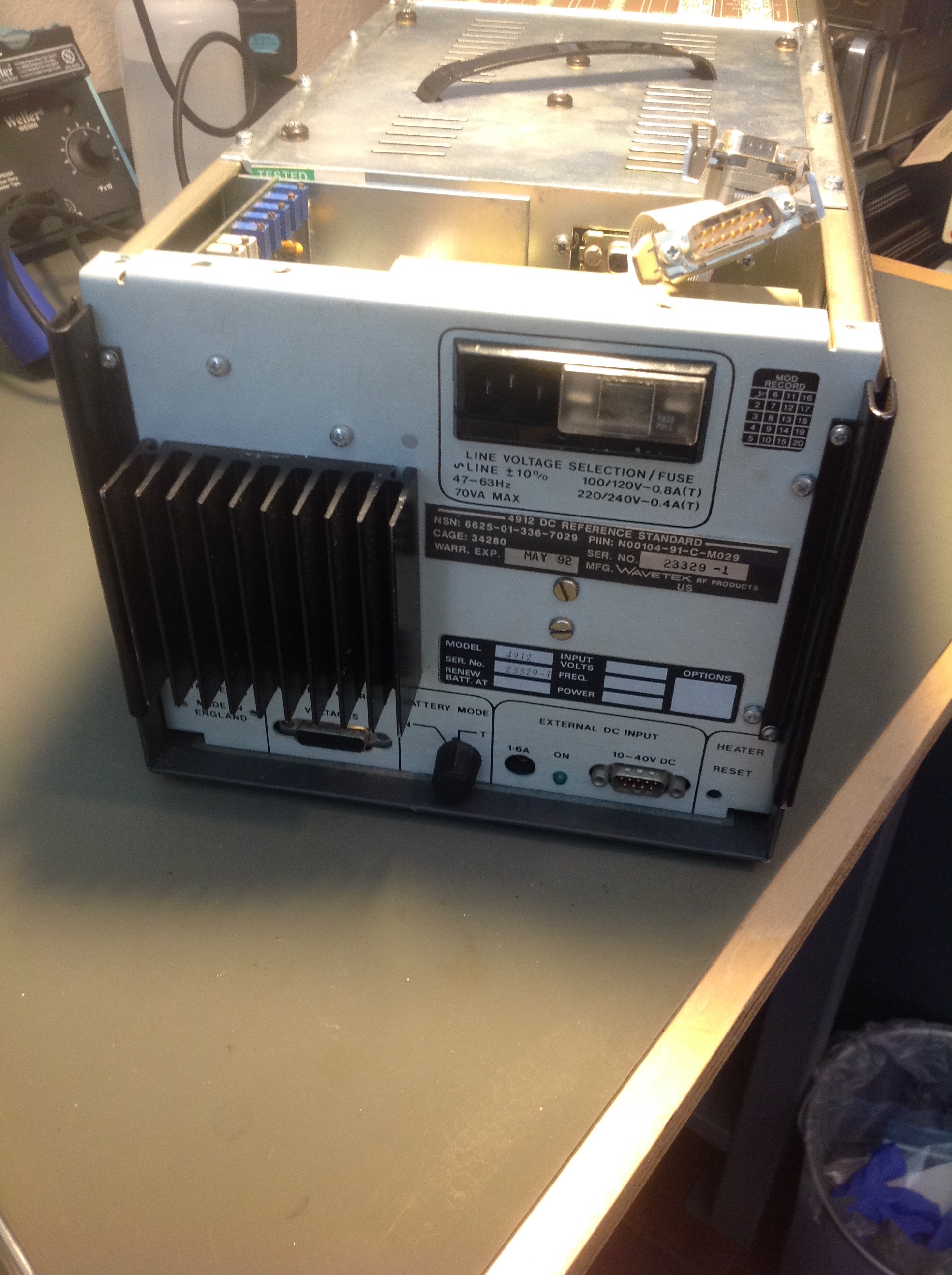
Image 146. Rear side of the 4912 unit
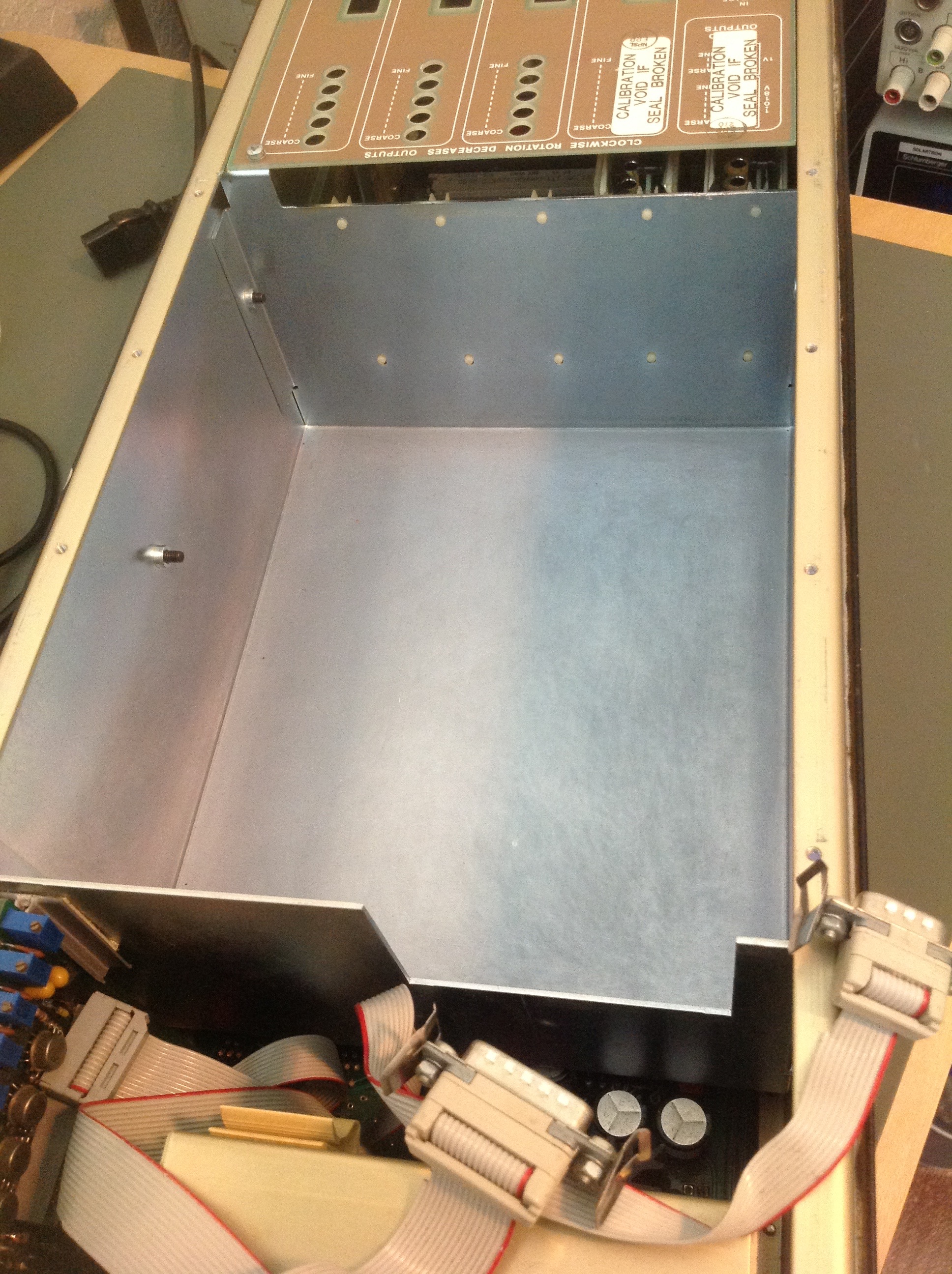
Image 147. Space for battery compartment
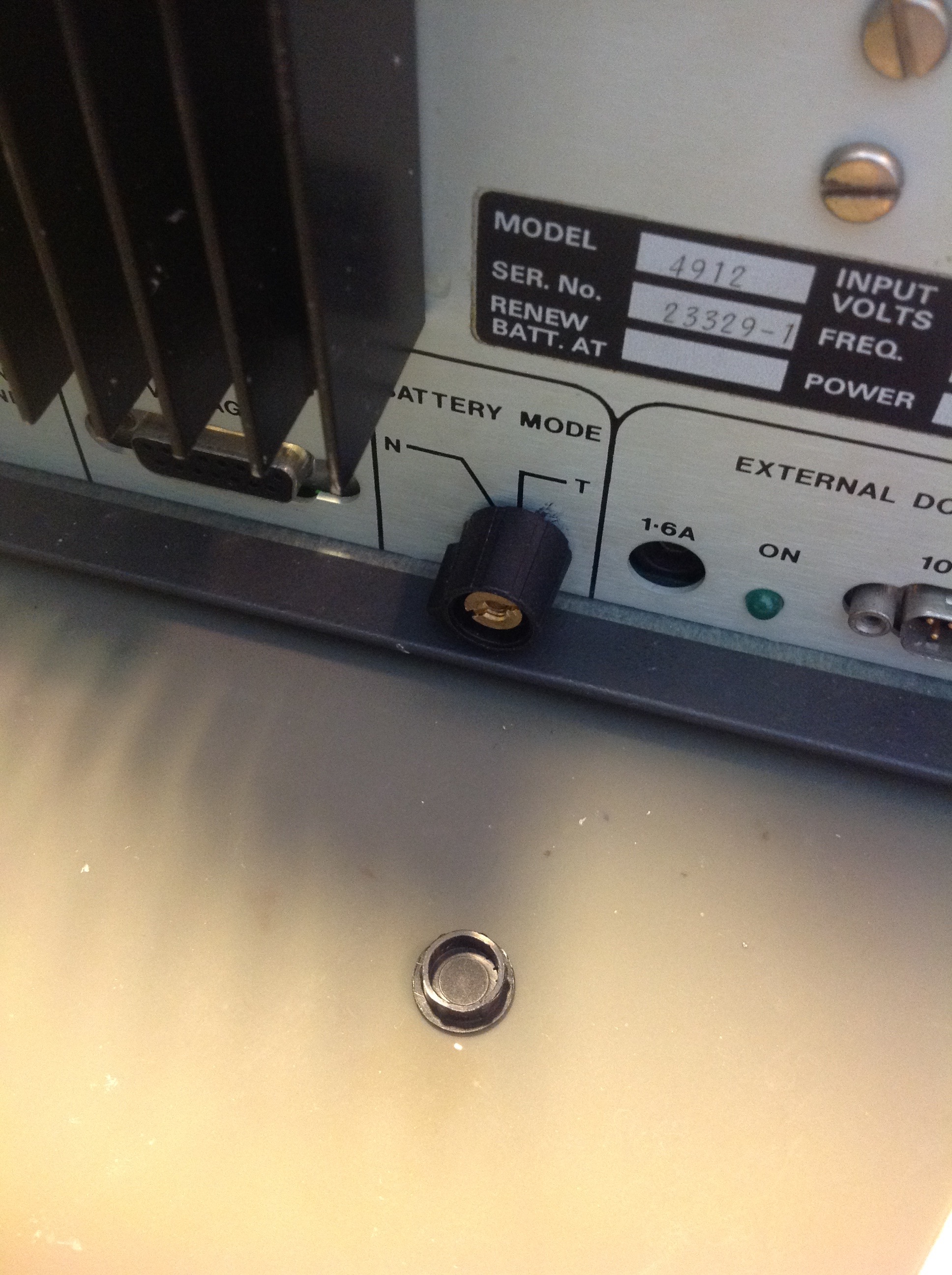
Image 148. Serial number label and power switch cap
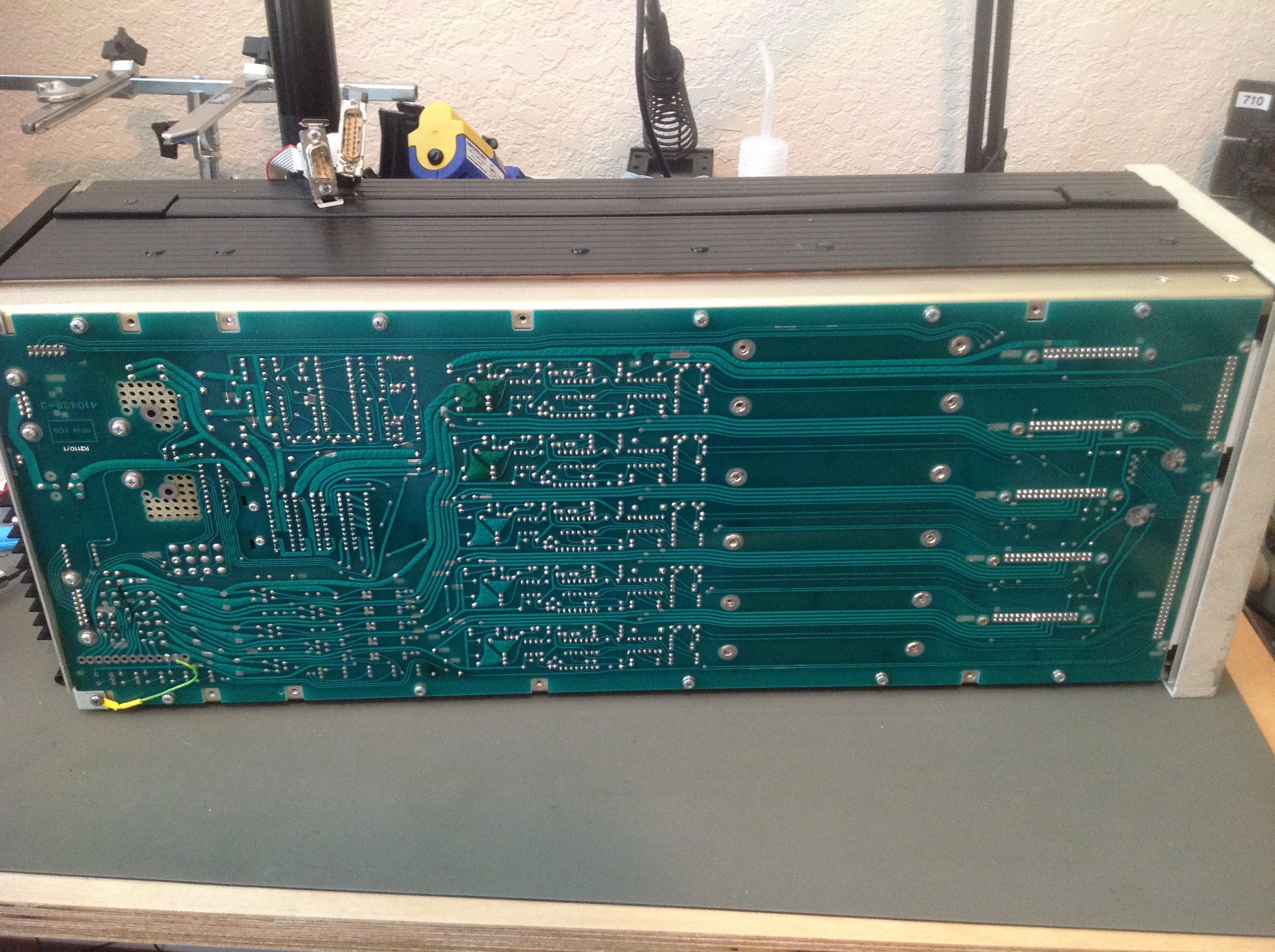
Image 149. Bottom side of the backplane mainboard
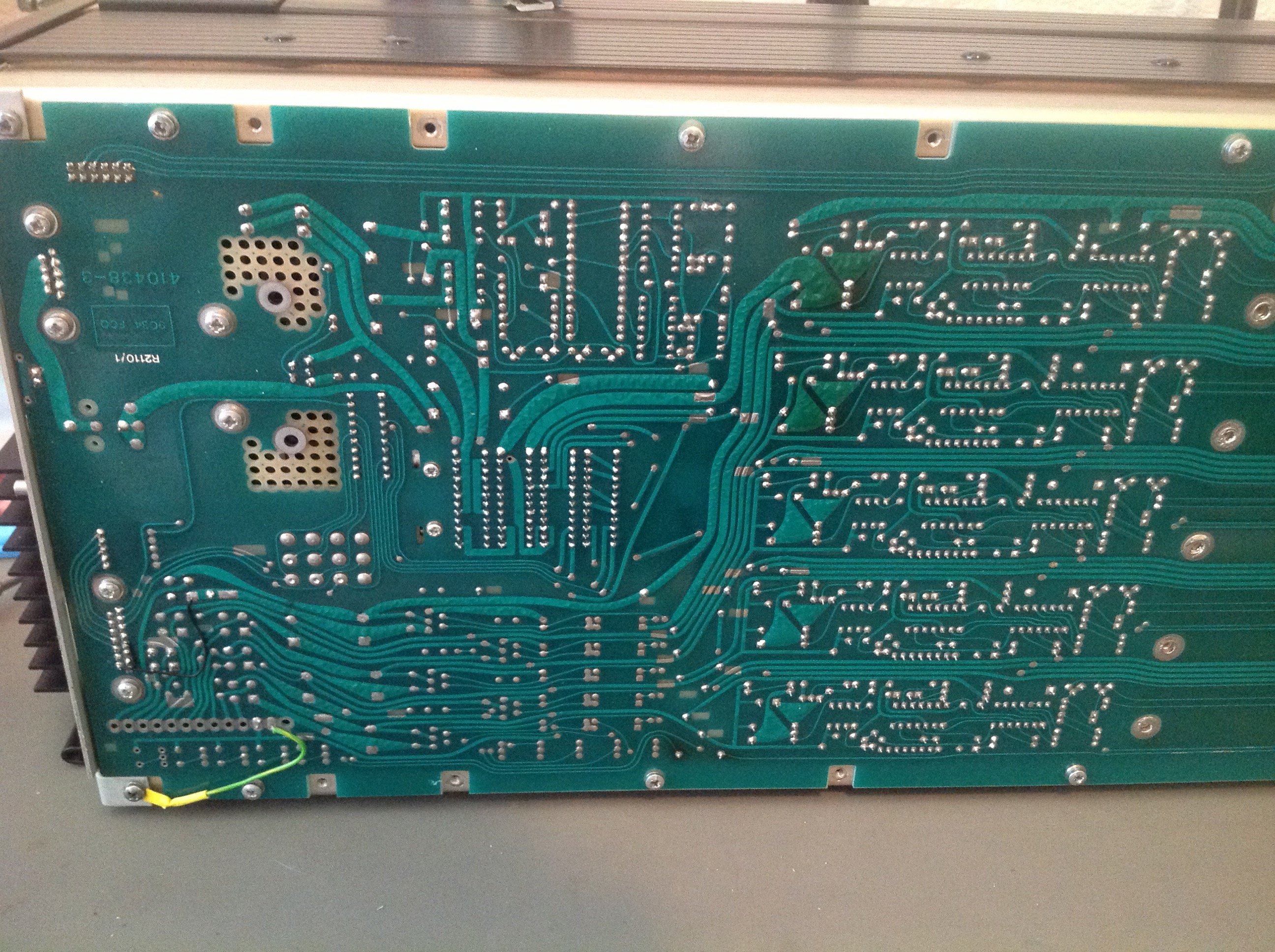
Image 150. Ground lead connector
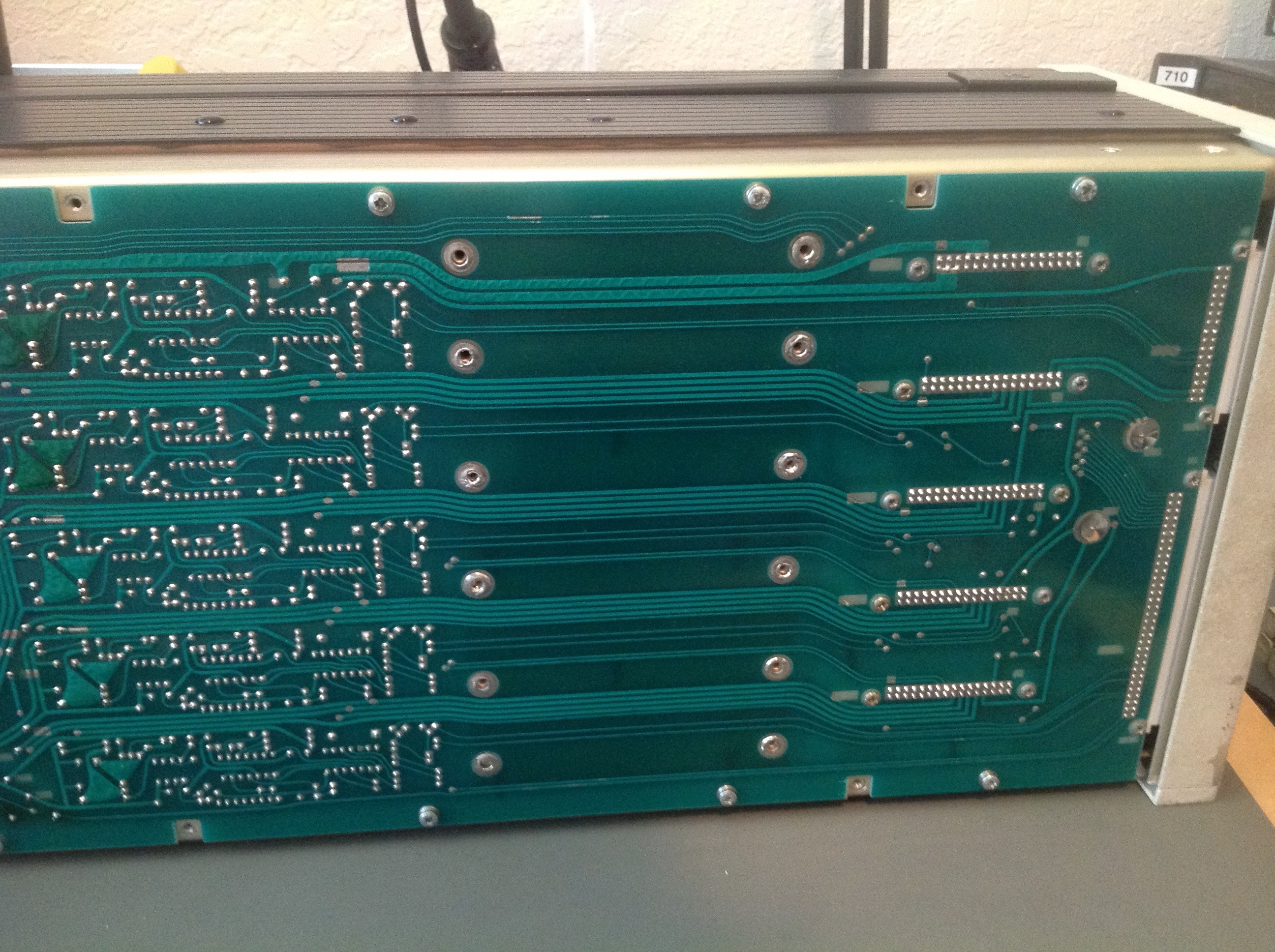
Image 151. Front side back PCB traces
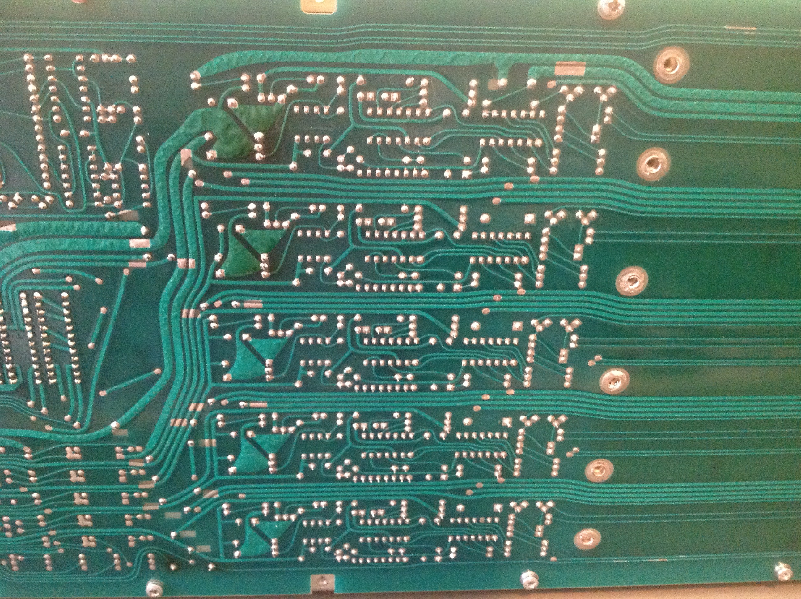
Image 152. Back of the board
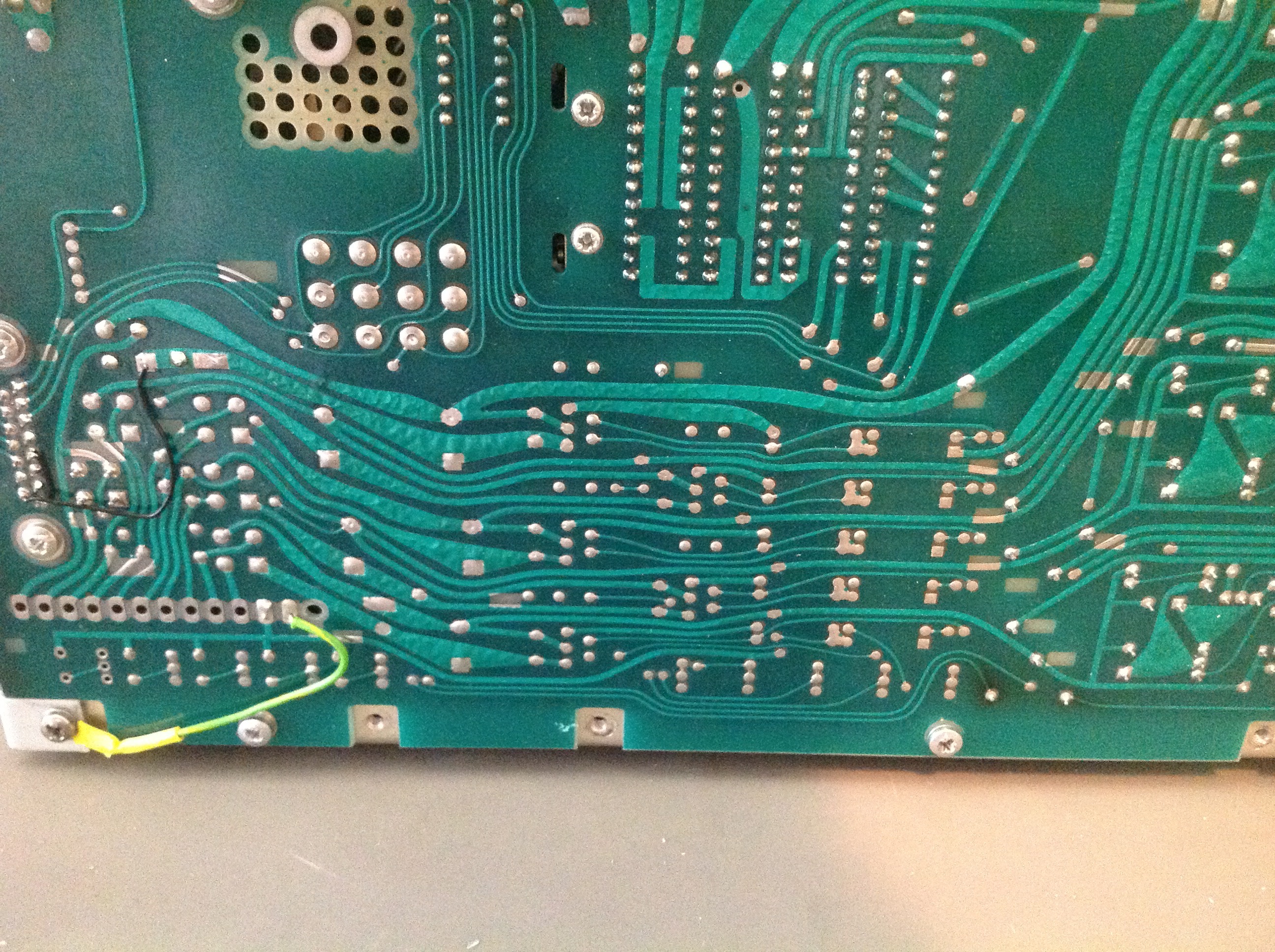
Image 153. Back of the board
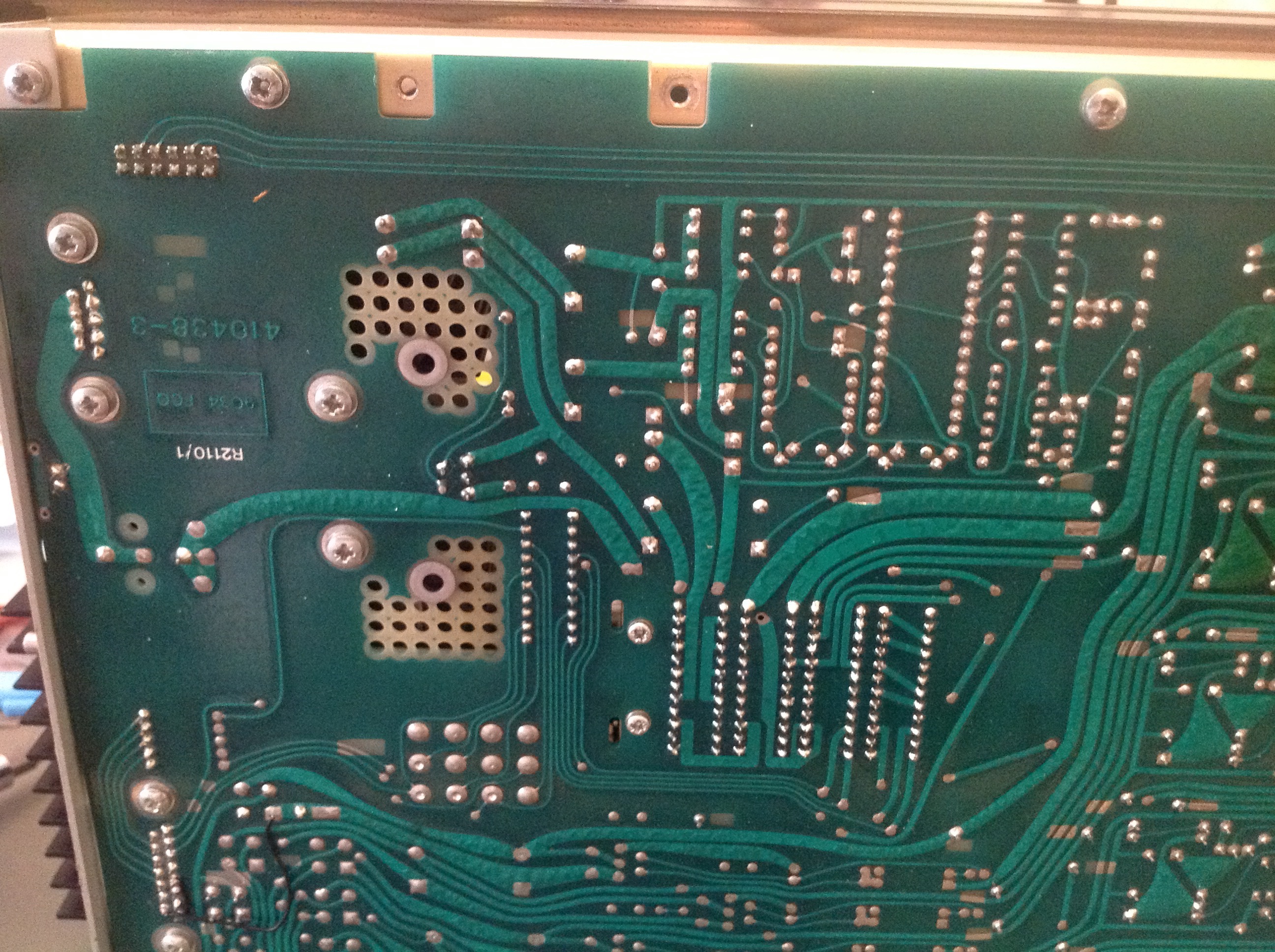
Image 154. Back of the board
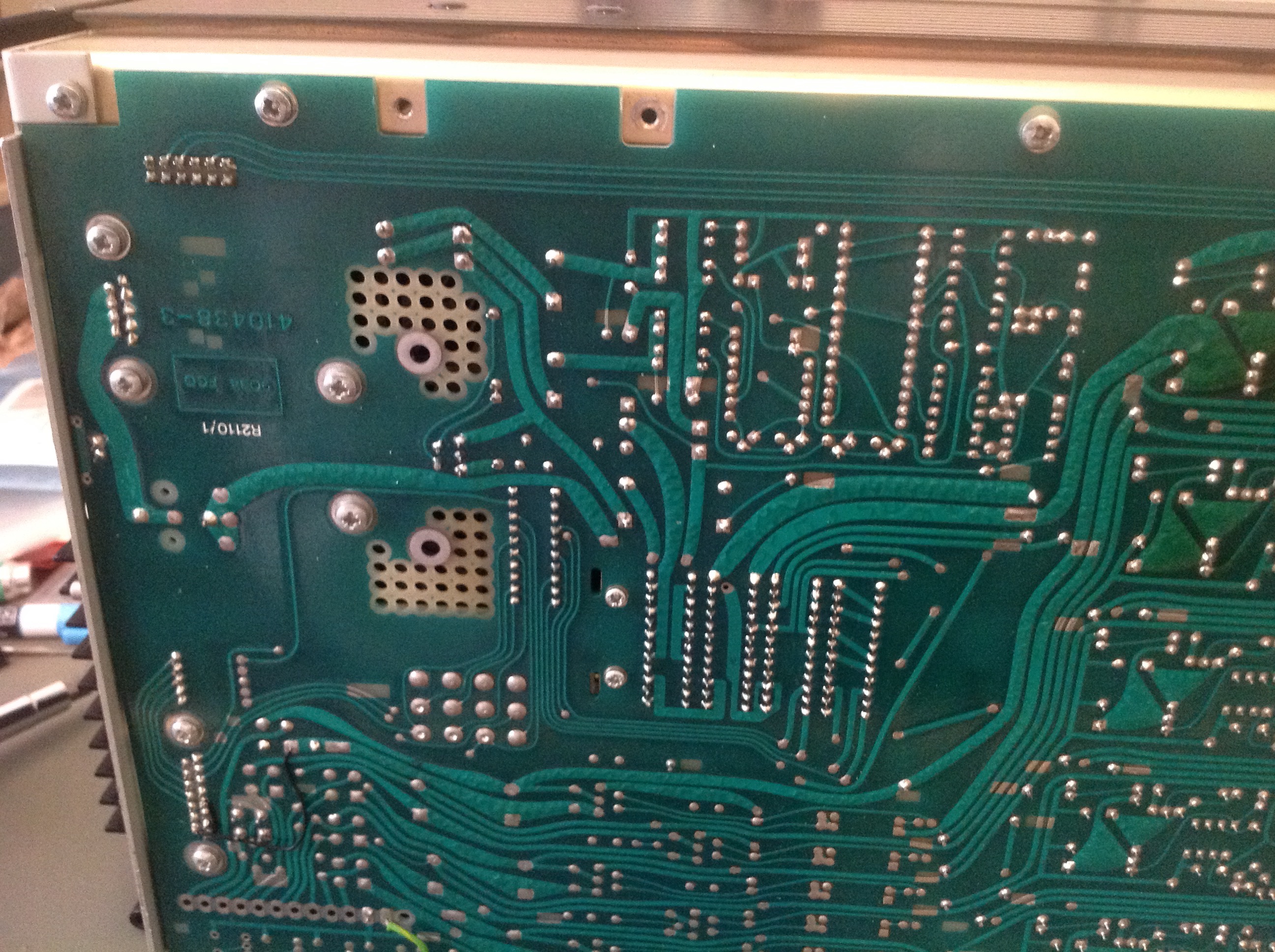
Image 155. Back of the board
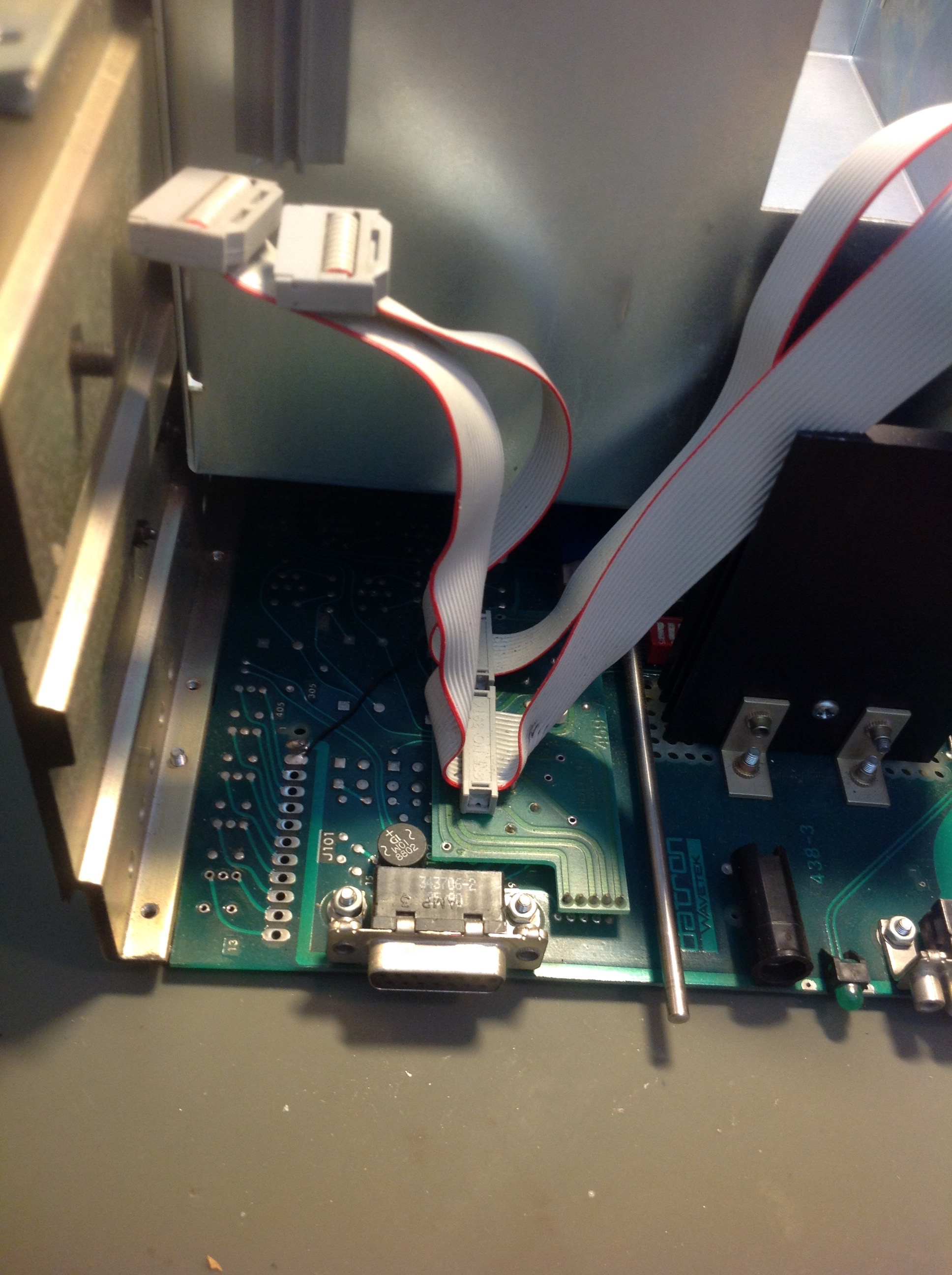
Image 156. Cables for charger PCBA
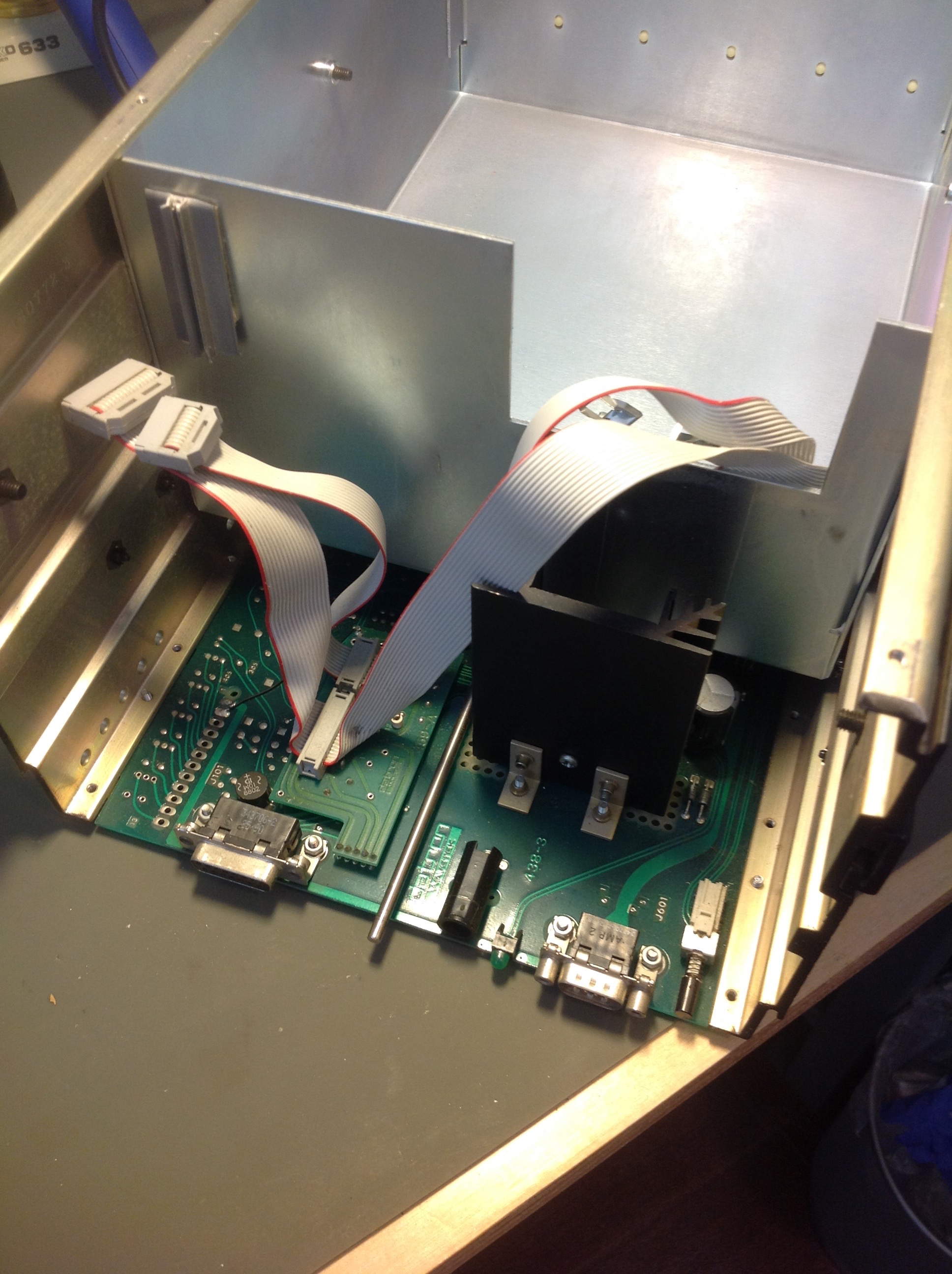
Image 157. Rear side connectors
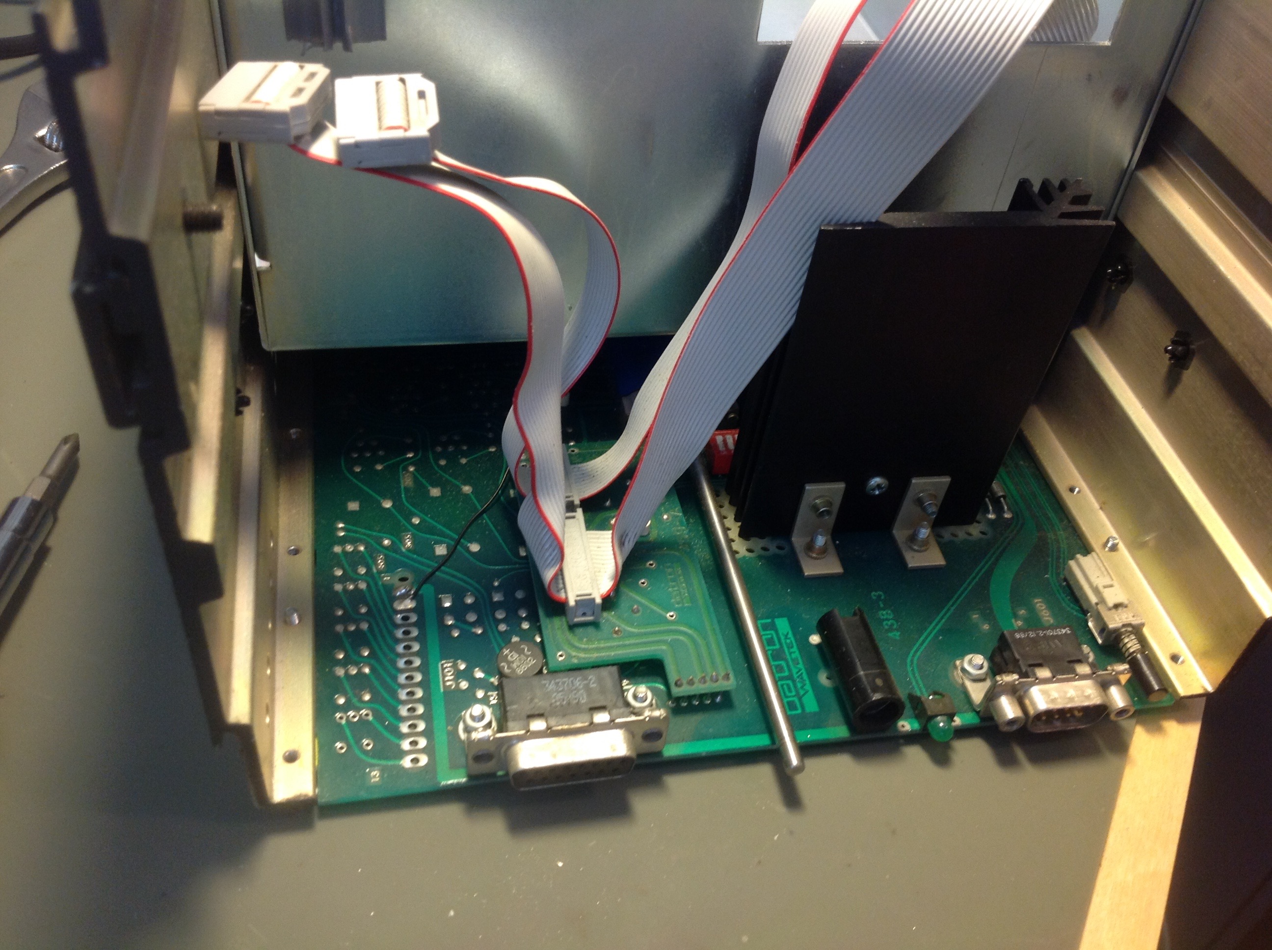
Image 158. Cabling for battery pack and board interconnects
Image 159. Charger board, removed
Image 160. Charger board, rear side with doctored resistors
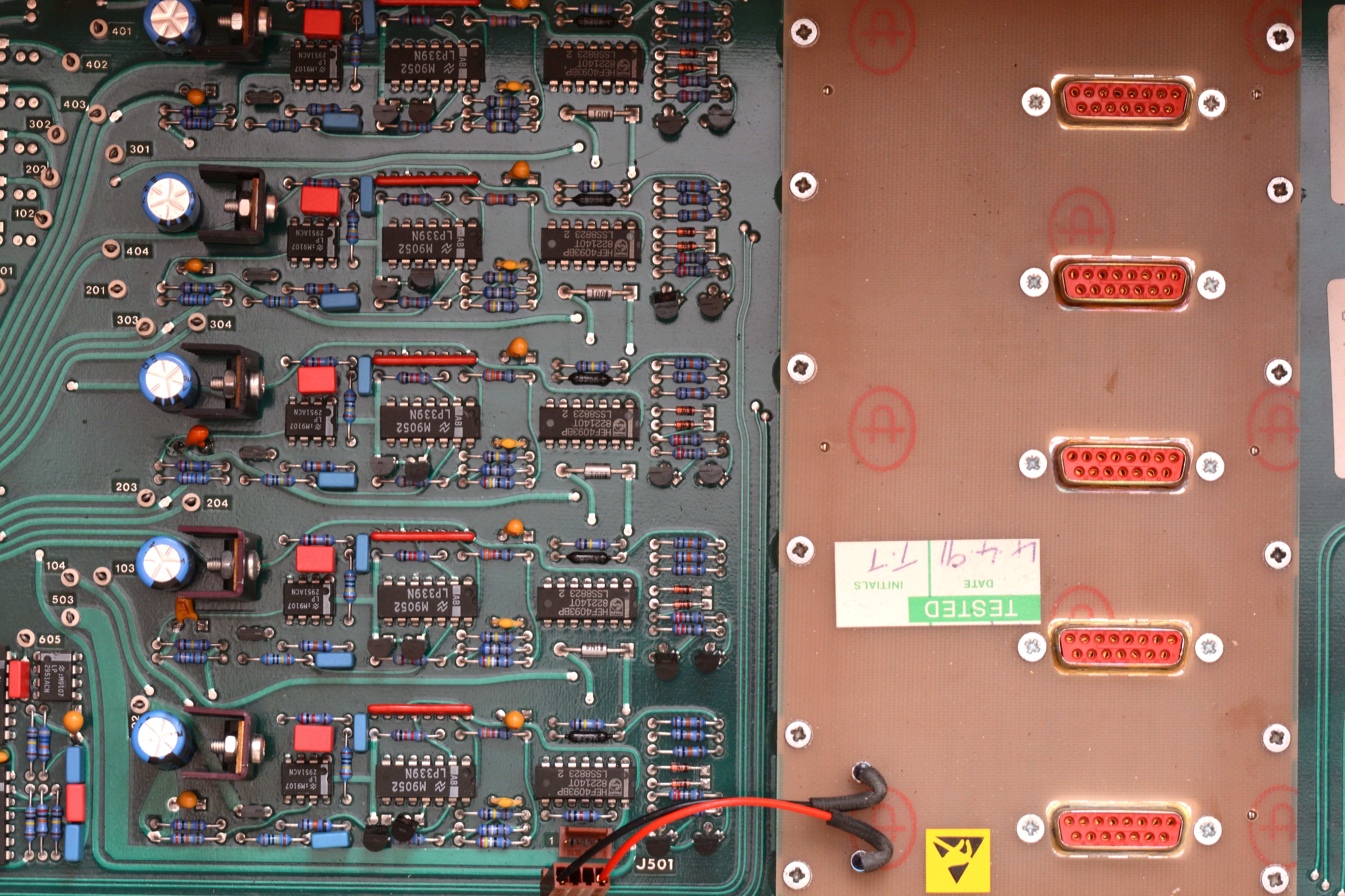
Image 161. Backplane connectors
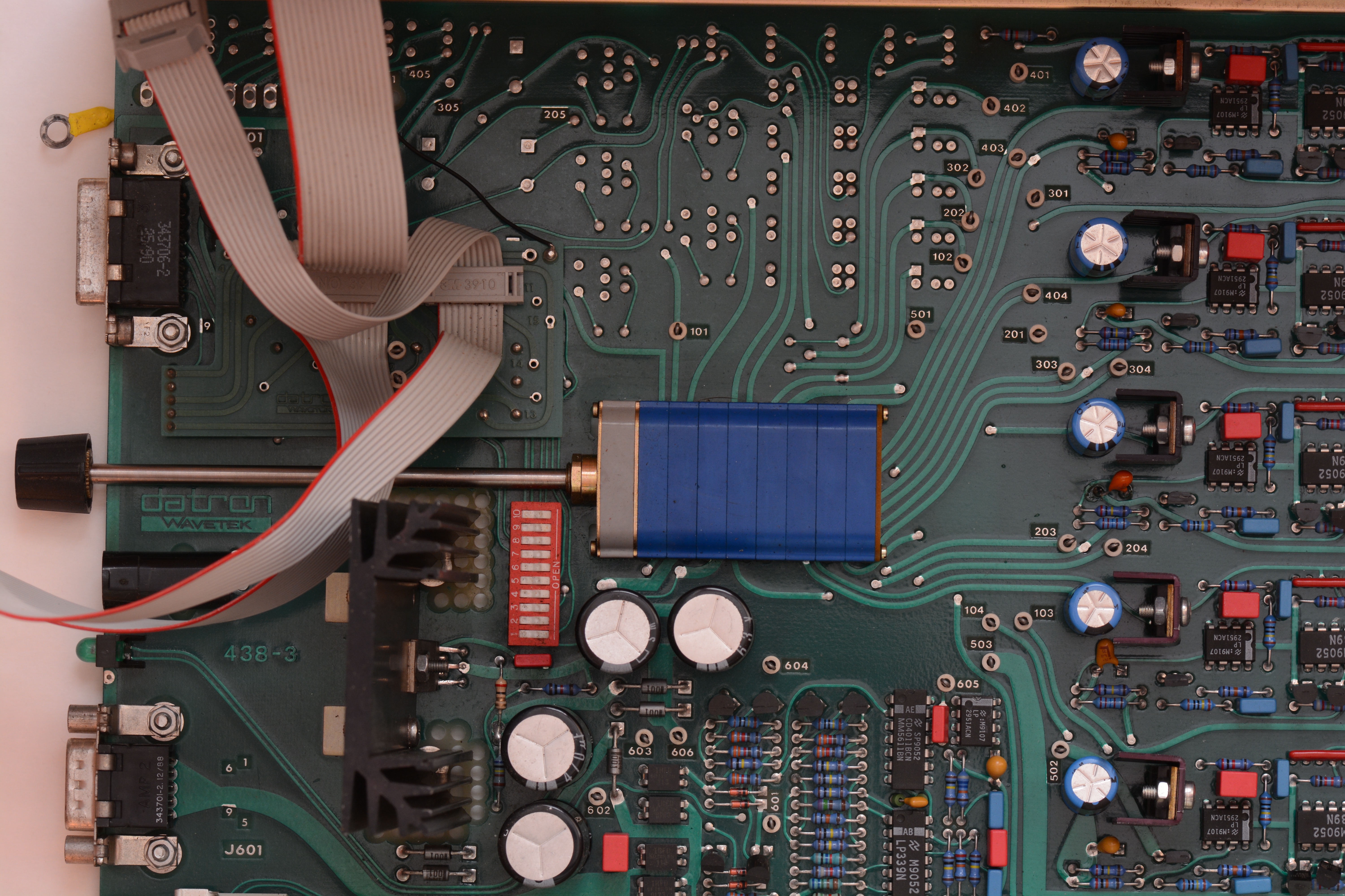
Image 162. Power mode switch
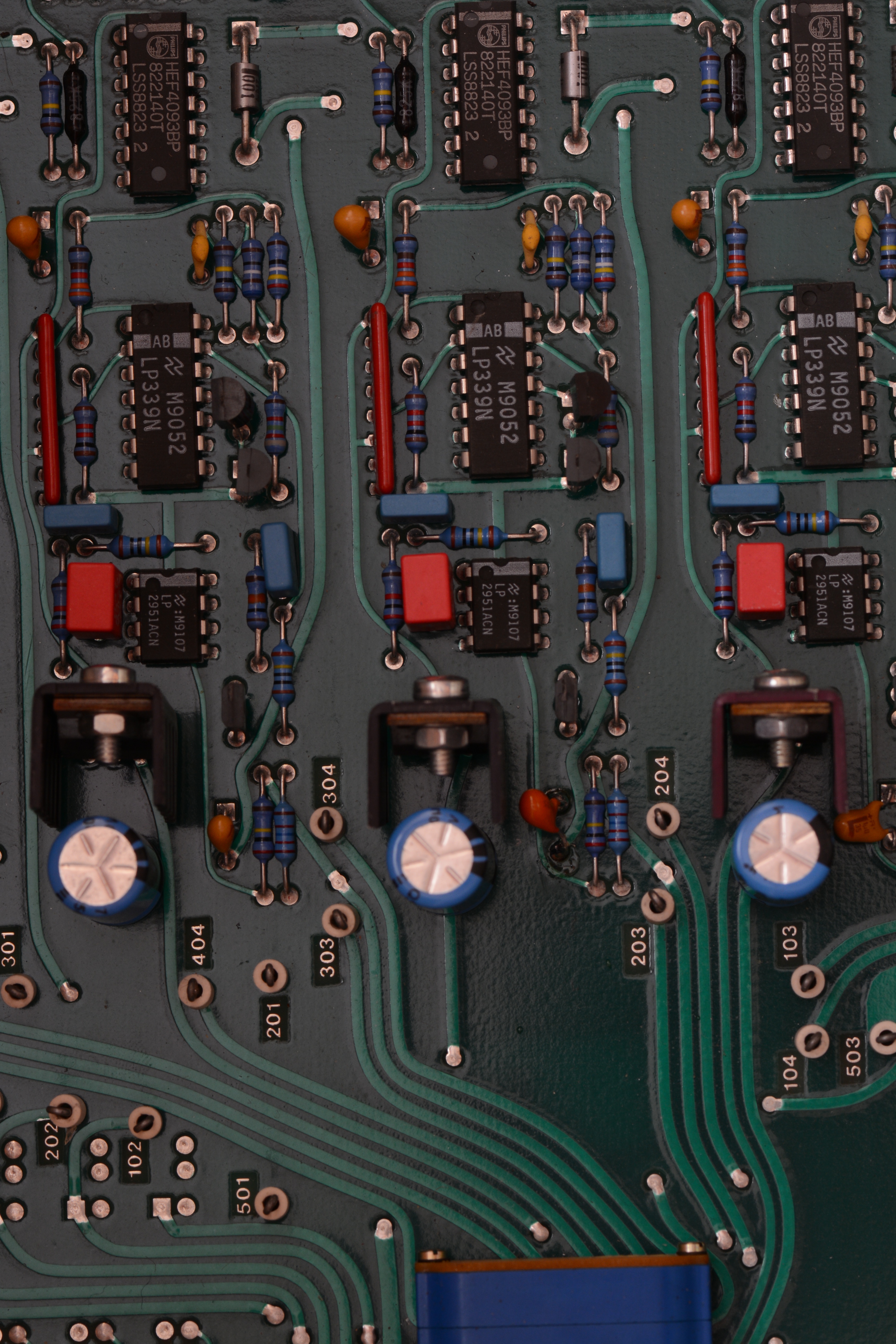
Image 163. Voltage regulators for cells
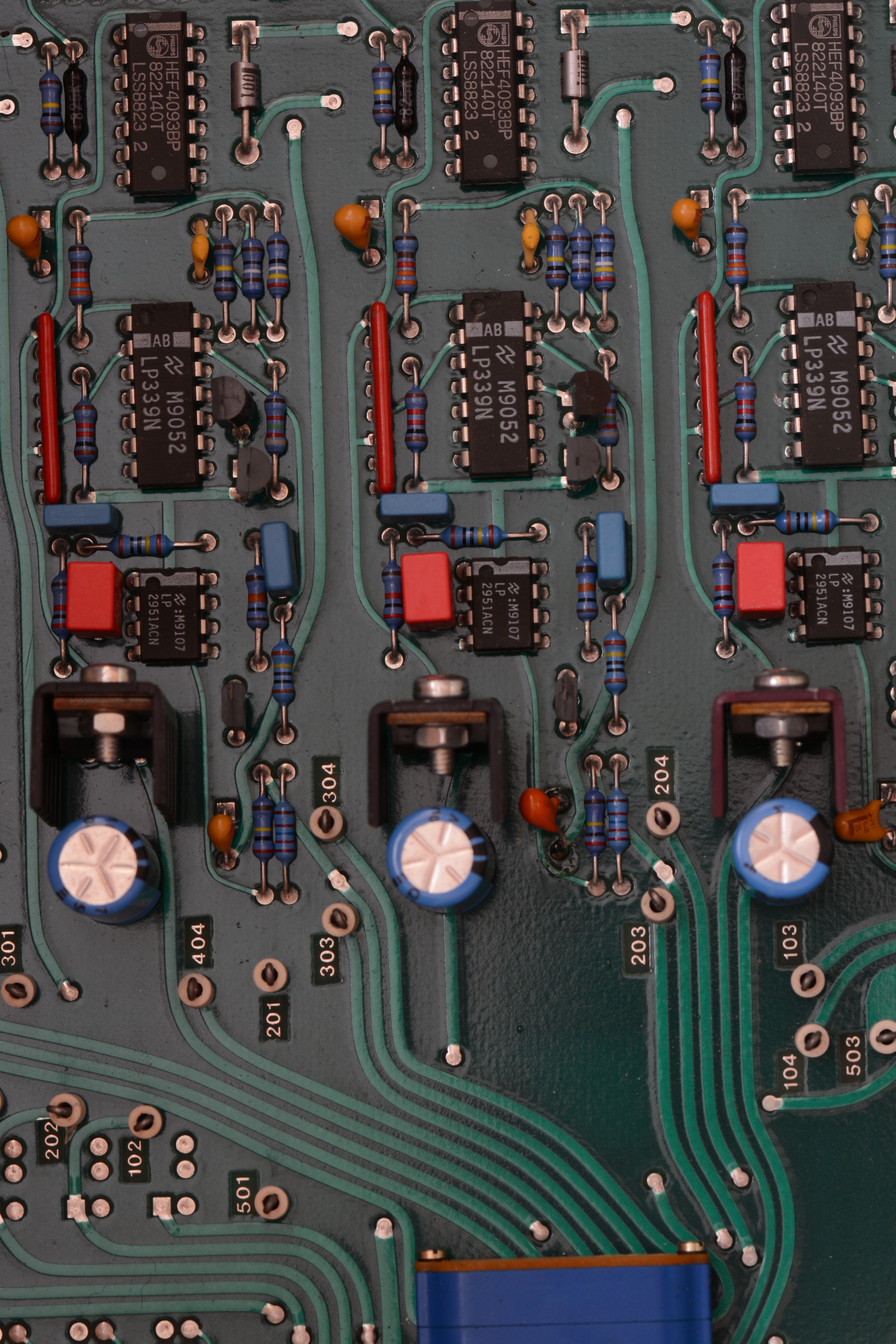
Image 164. Regulator controllers and comparators for monitoring
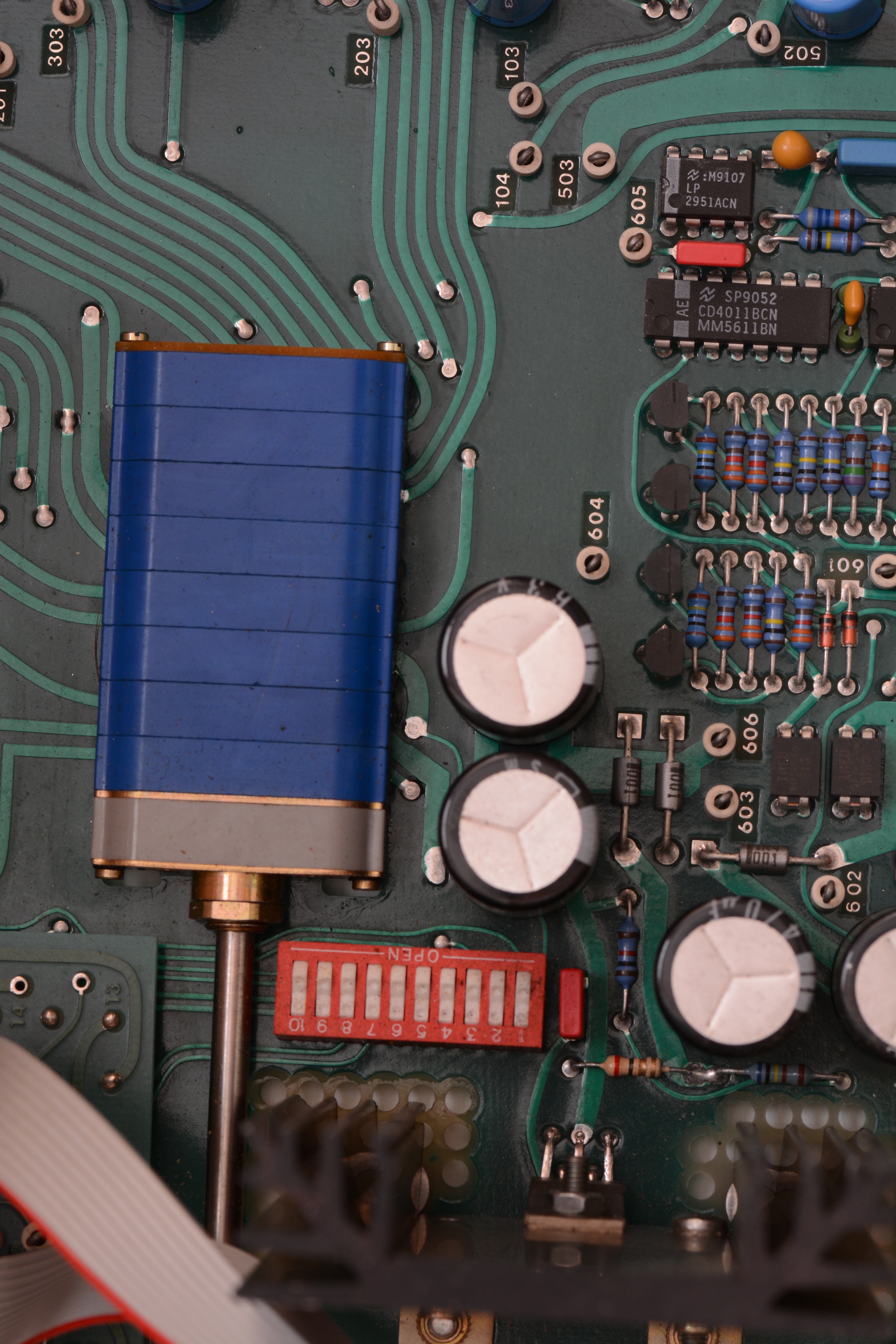
Image 165. Configuration switch
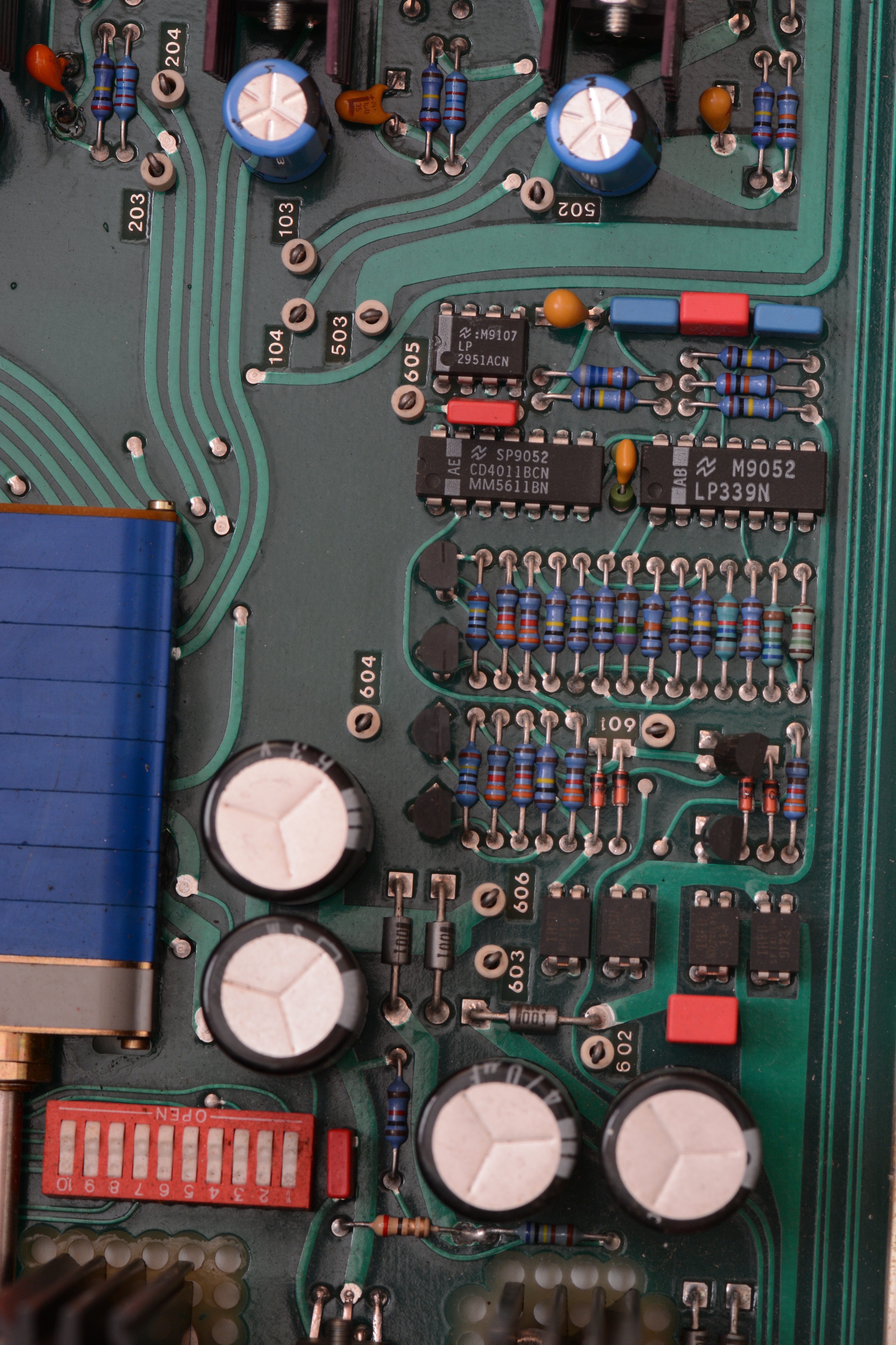
Image 166. Test points available for testing
Close-ups for reference cell PCBA
It’s the same board as in earlier work with 4910, so here I just give a summary photos:
Image 167. Front of the cell PCB circuitry
Image 168. Front of the cell PCB circuitry
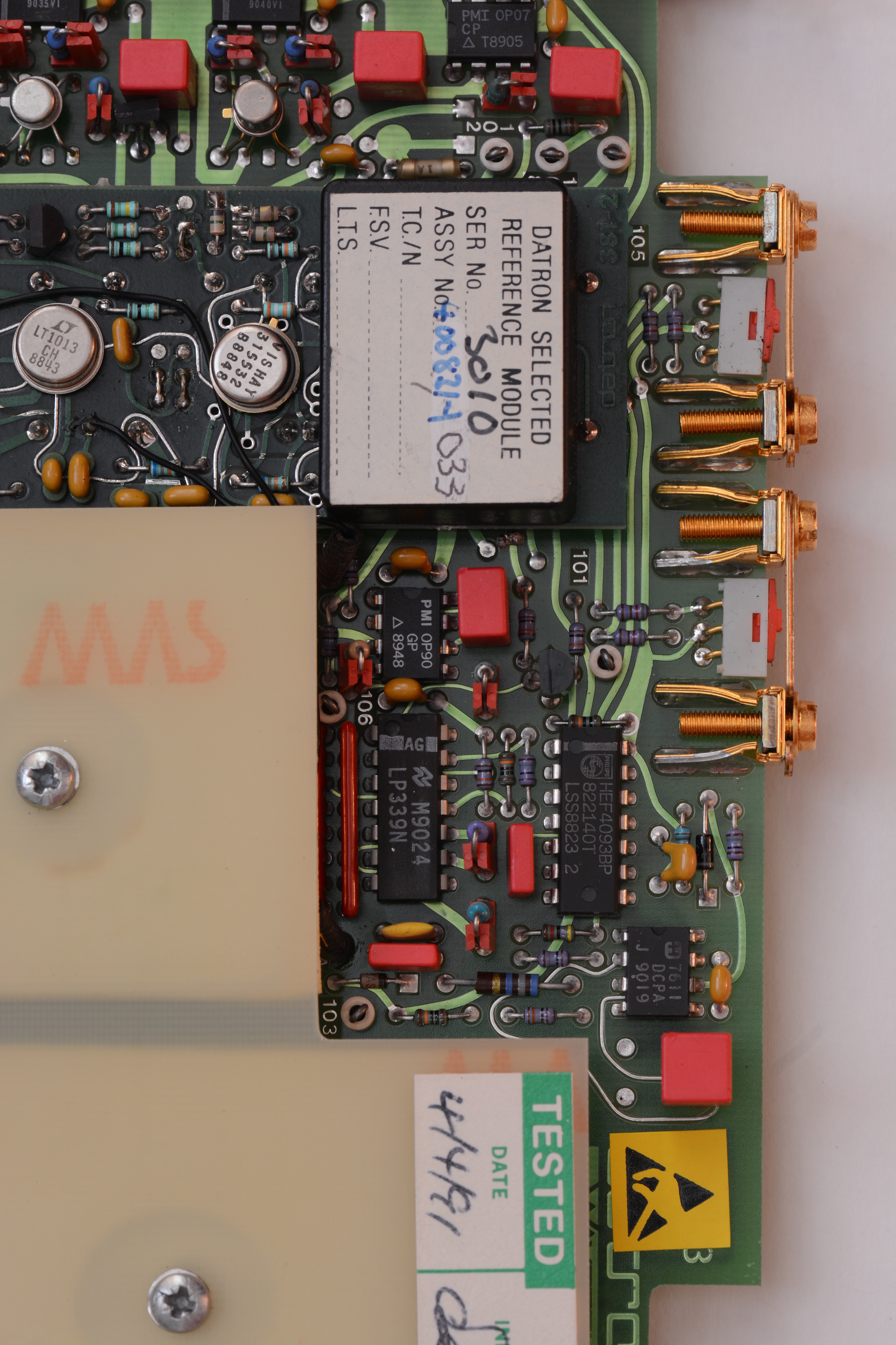
Image 169. Front of the cell PCB circuitry

Image 170. Front of the cell PCB circuitry
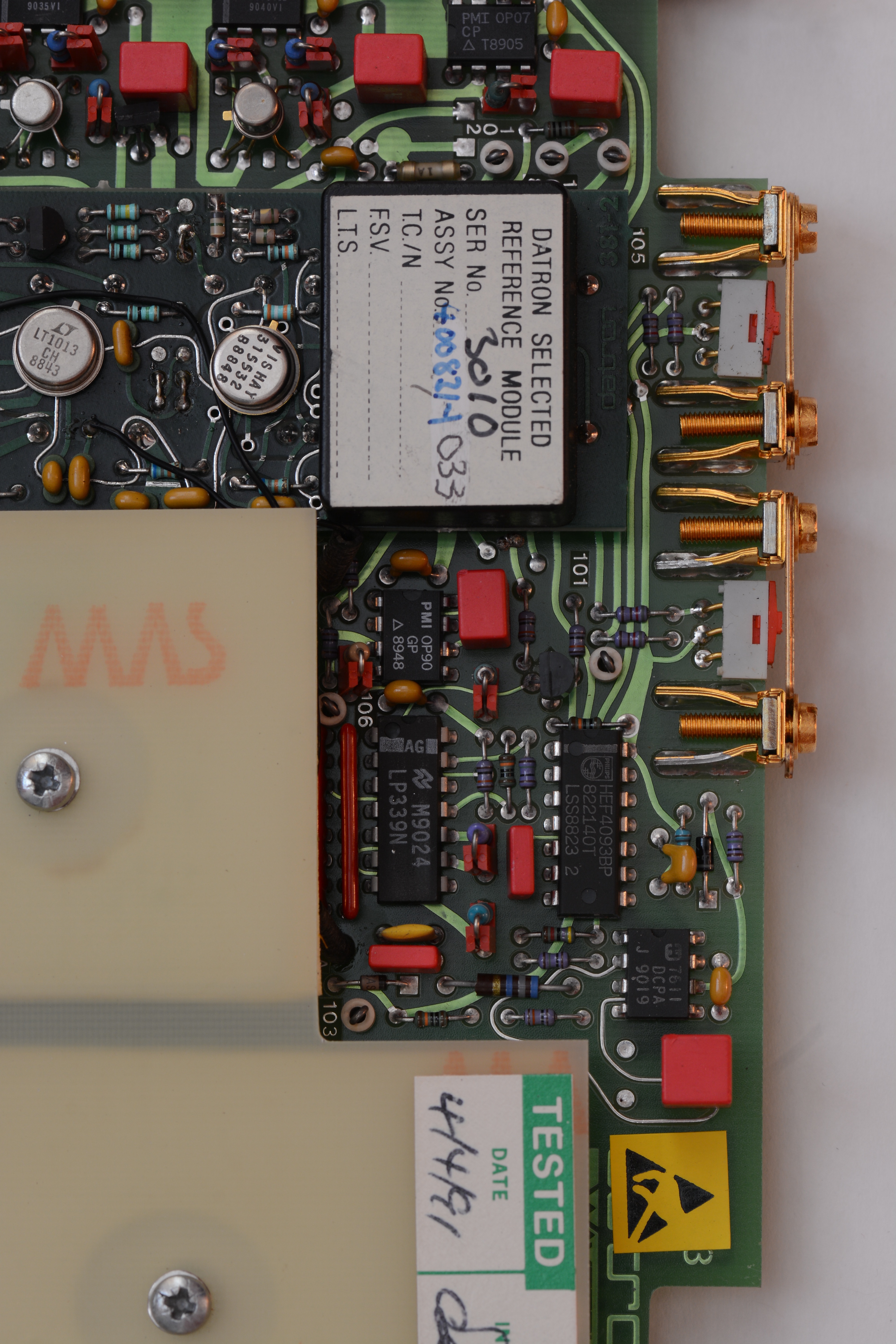
Image 171. Front of the cell PCB circuitry
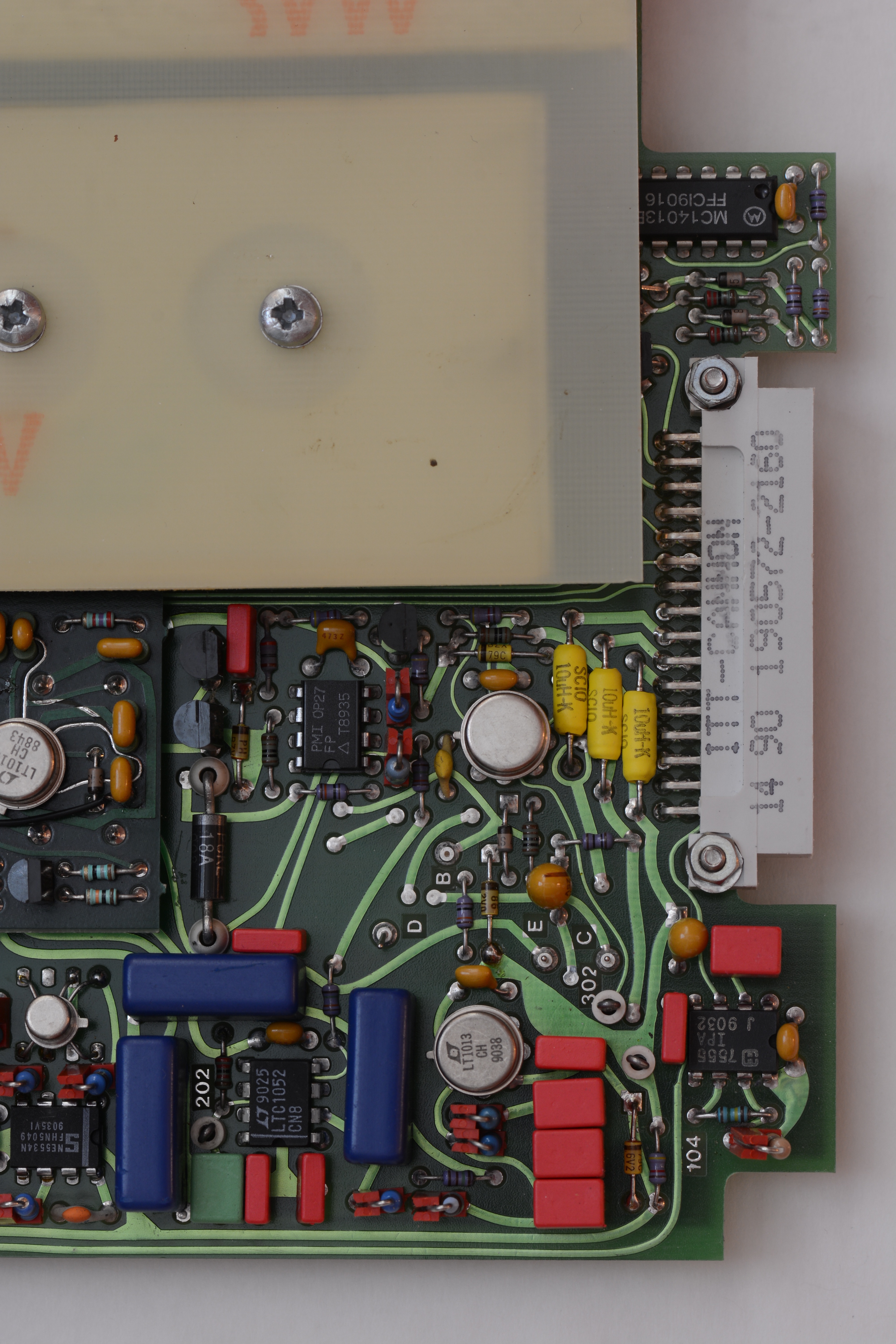
Image 172. Front of the cell PCB circuitry
Image 173. Rear of the cell PCB
Image 174. Rear of the cell PCB
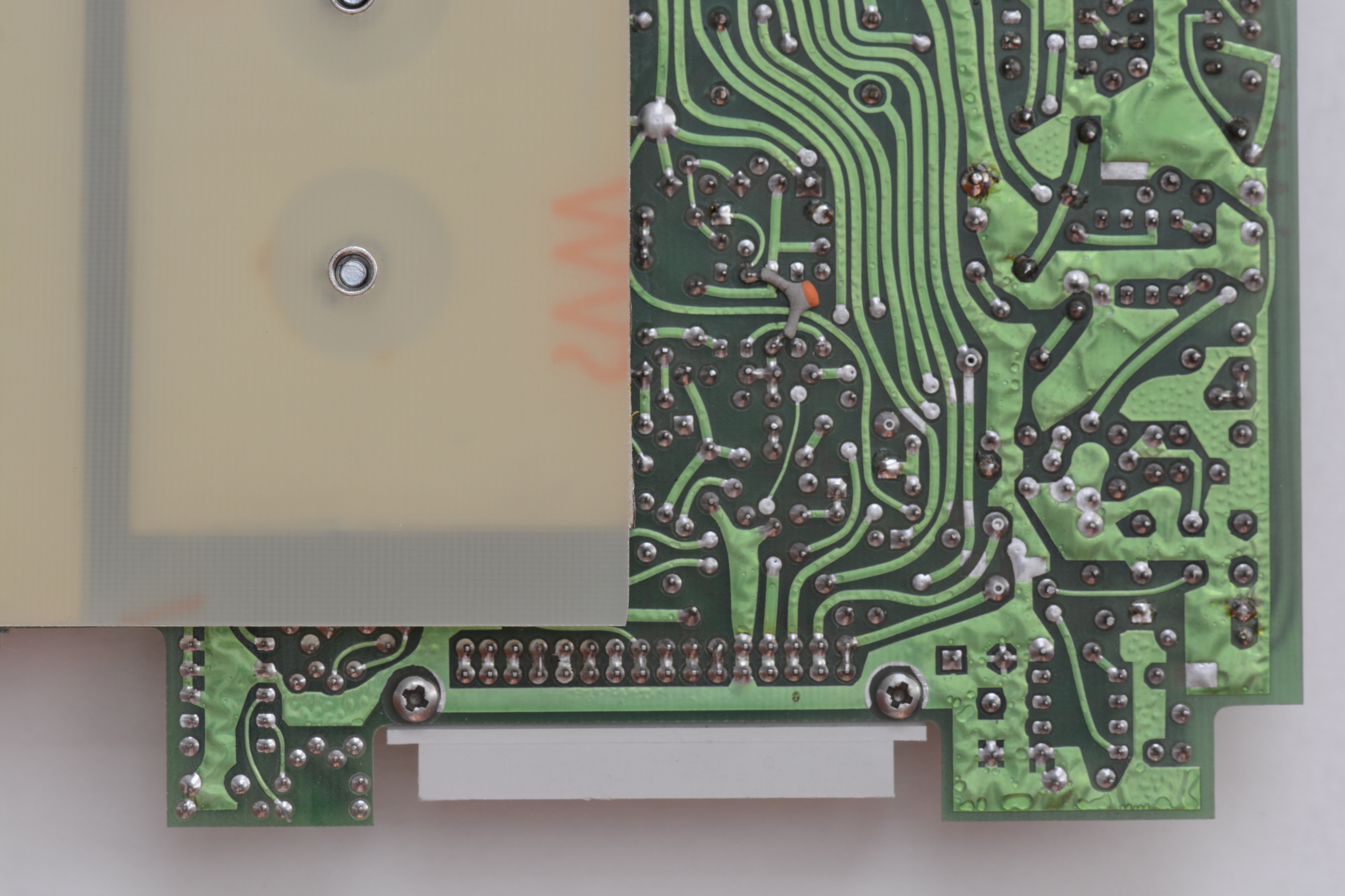
Image 175. Rear of the cell PCB
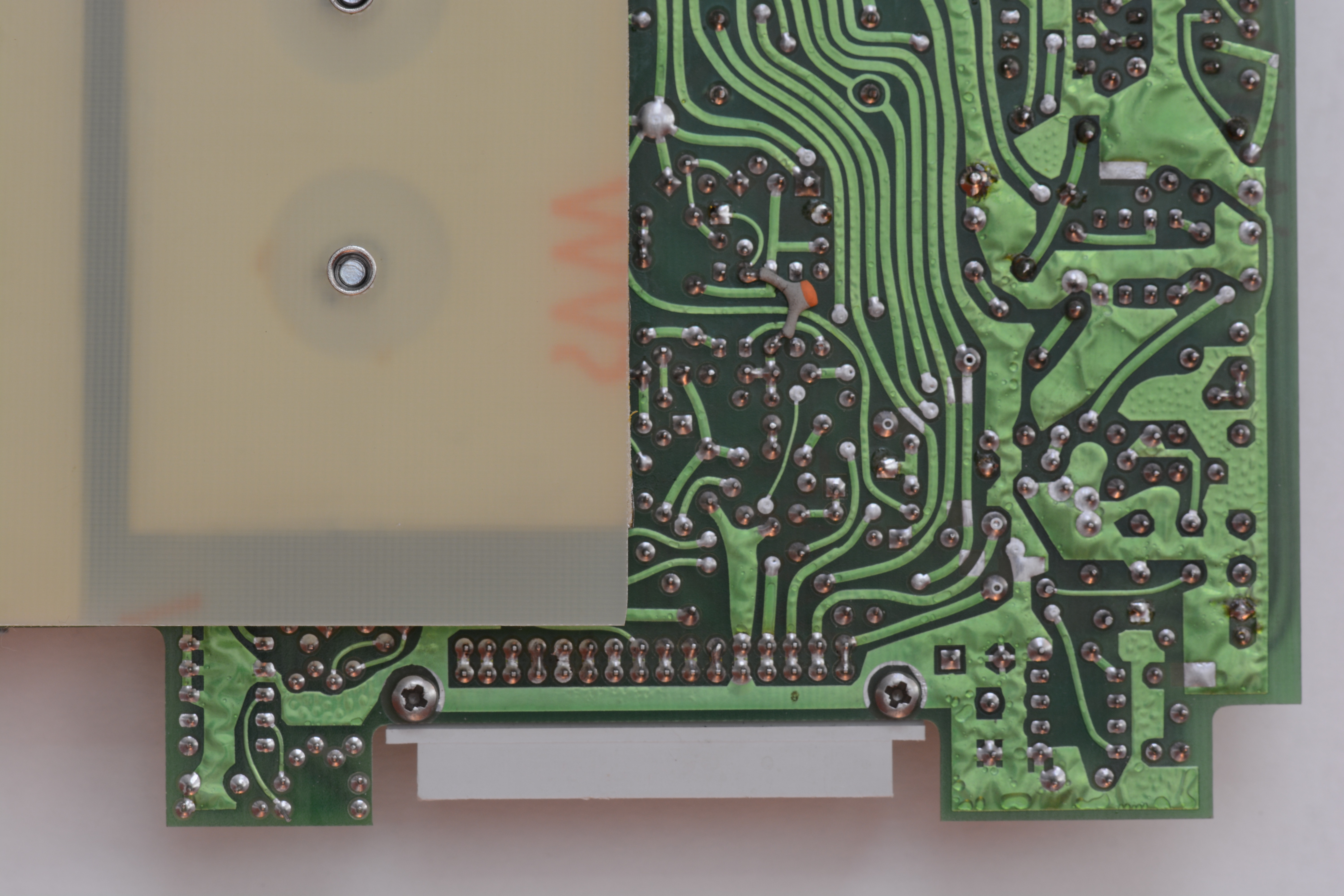
Image 176. Rear of the cell PCB
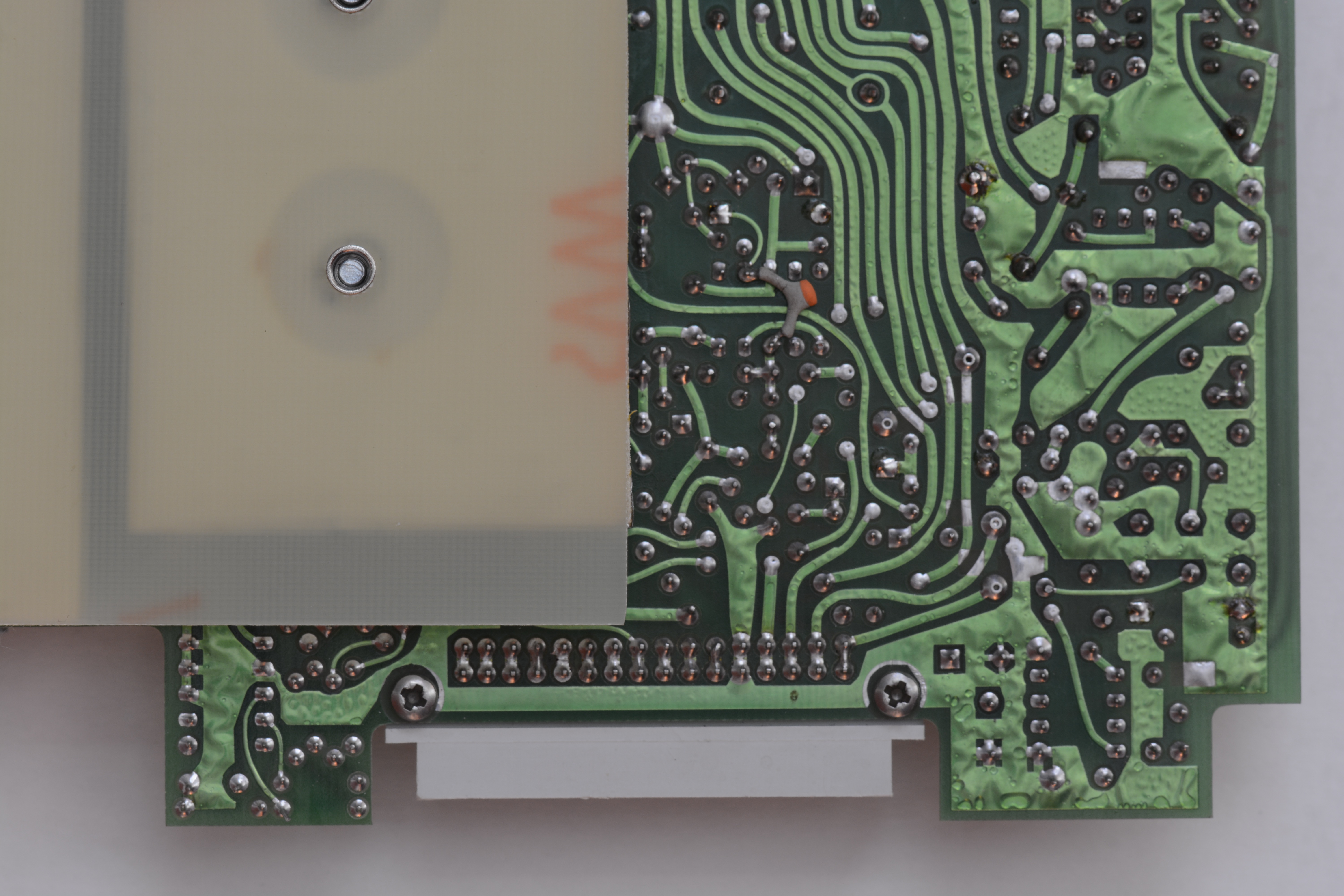
Image 177. Rear of the cell PCB
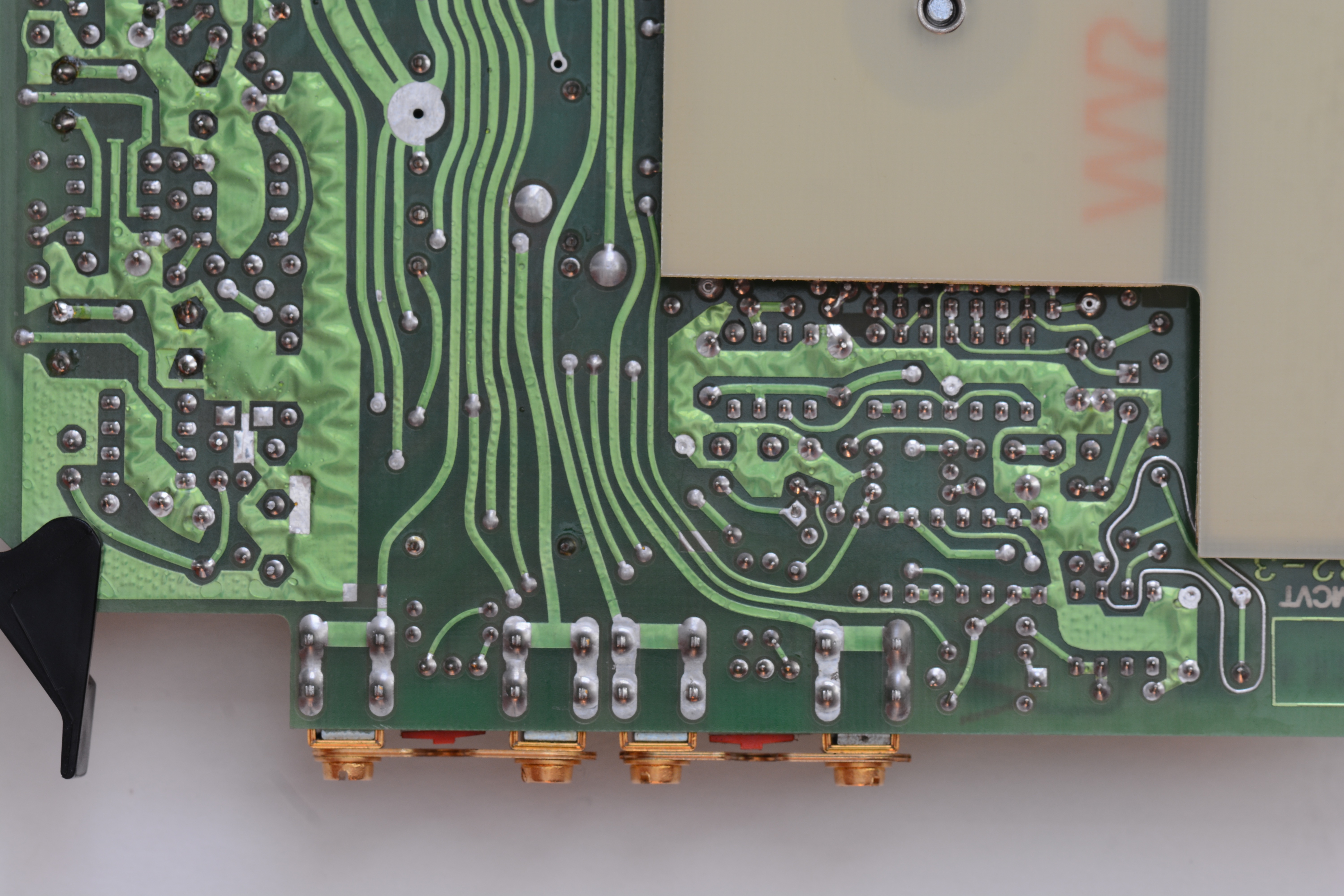
Image 178. Rear of the cell PCB
Backplane repairs
One of the issues were hiding in shielded area of DSub ports for cells.
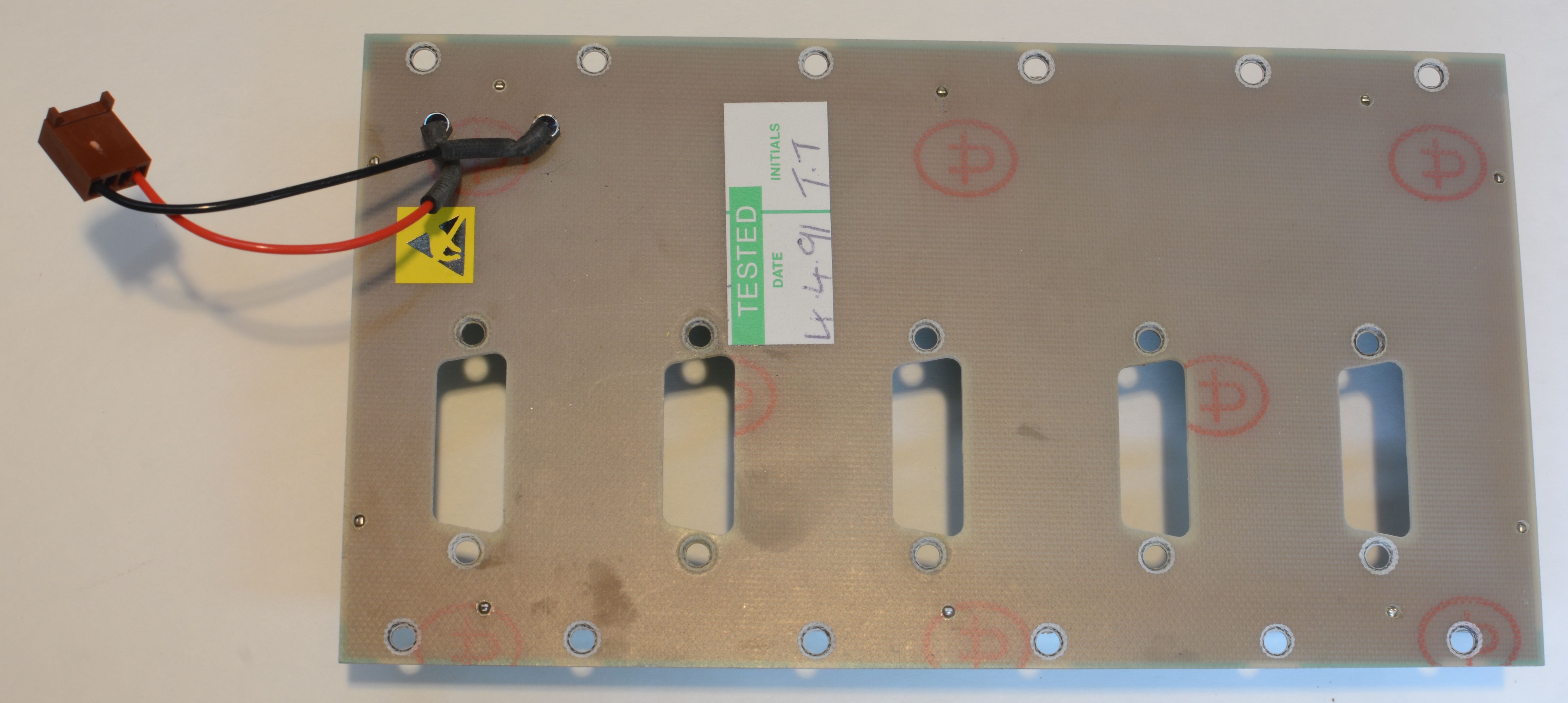
Image 179. Removed shield for cell connectors
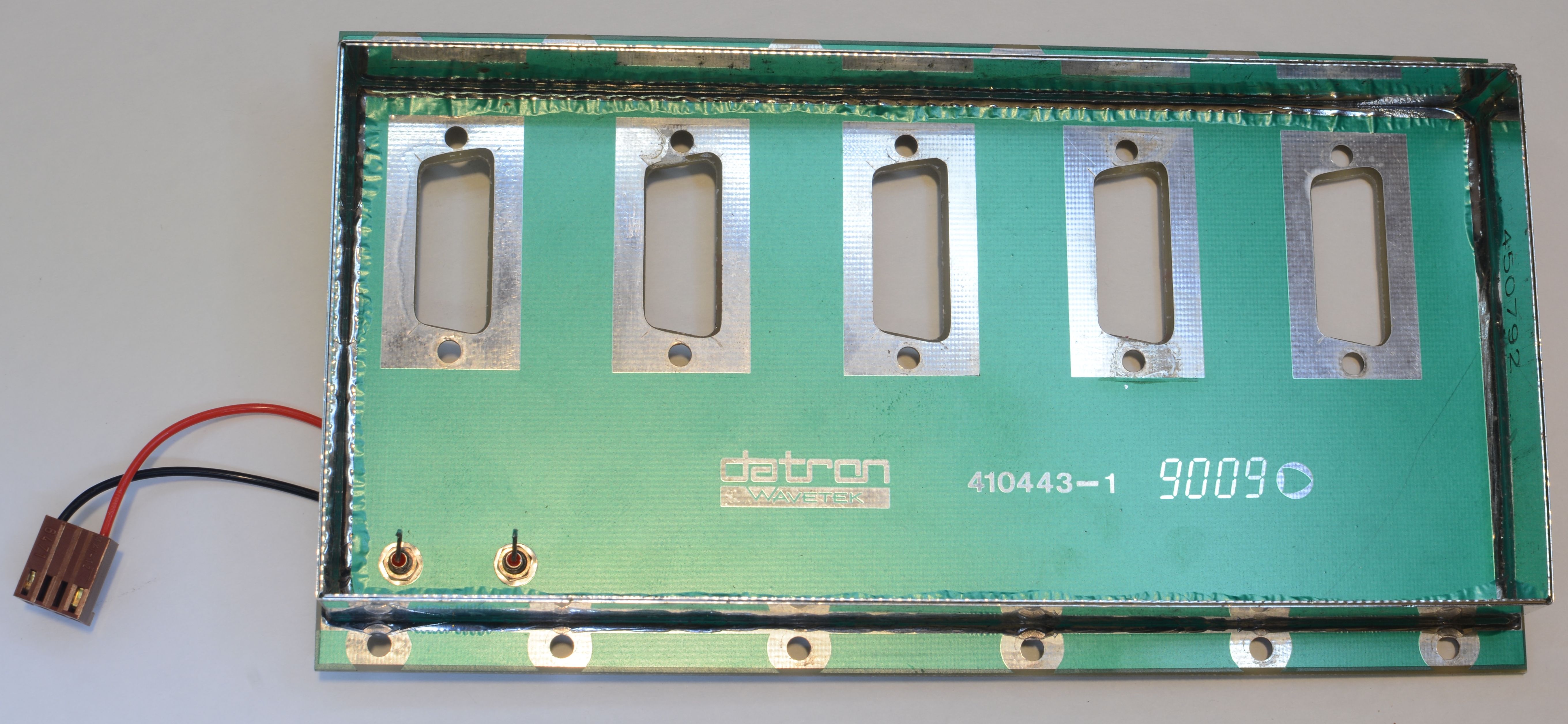
Image 180. Shielding box, removed
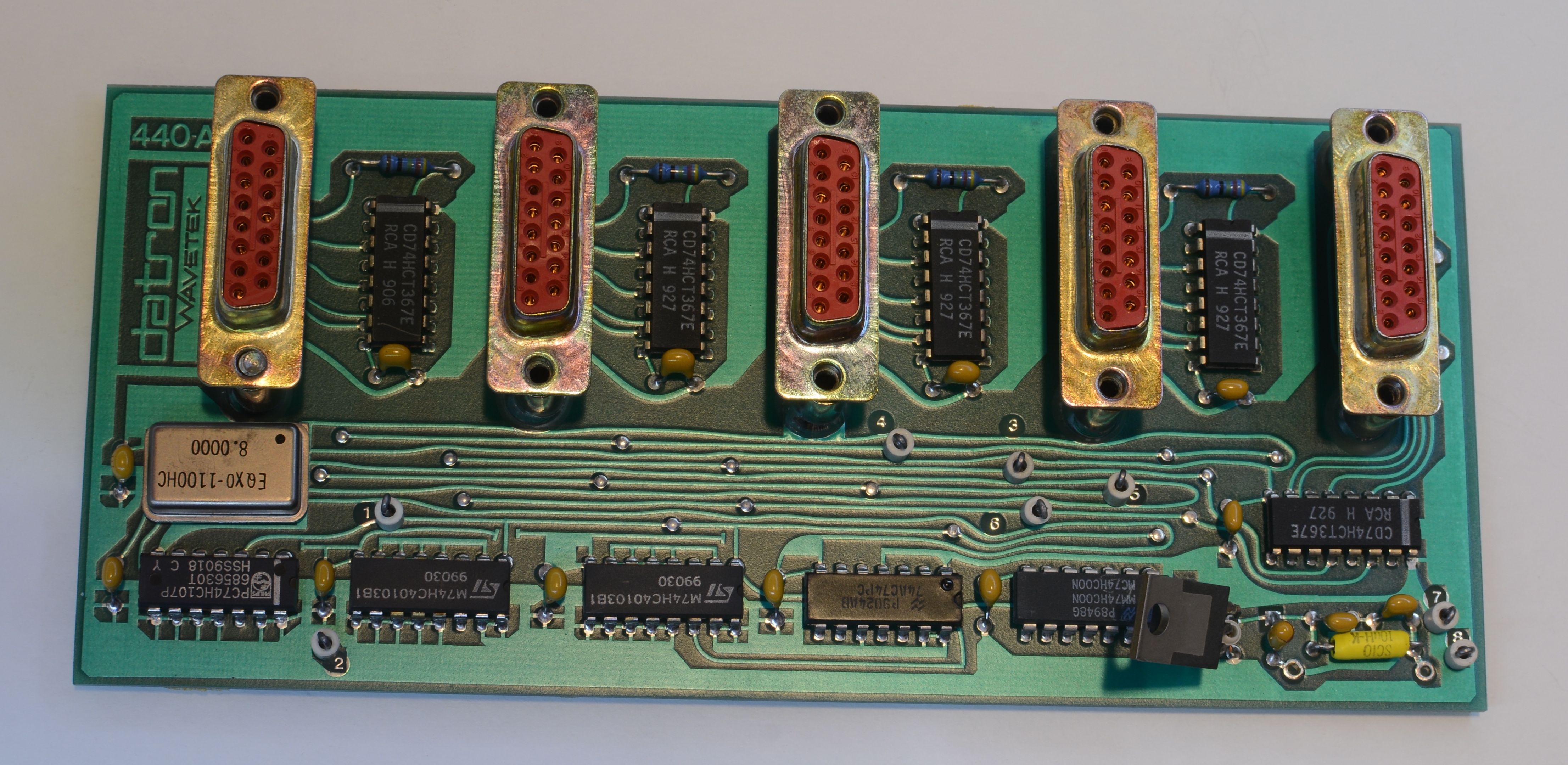
Image 181. Metal PCB box
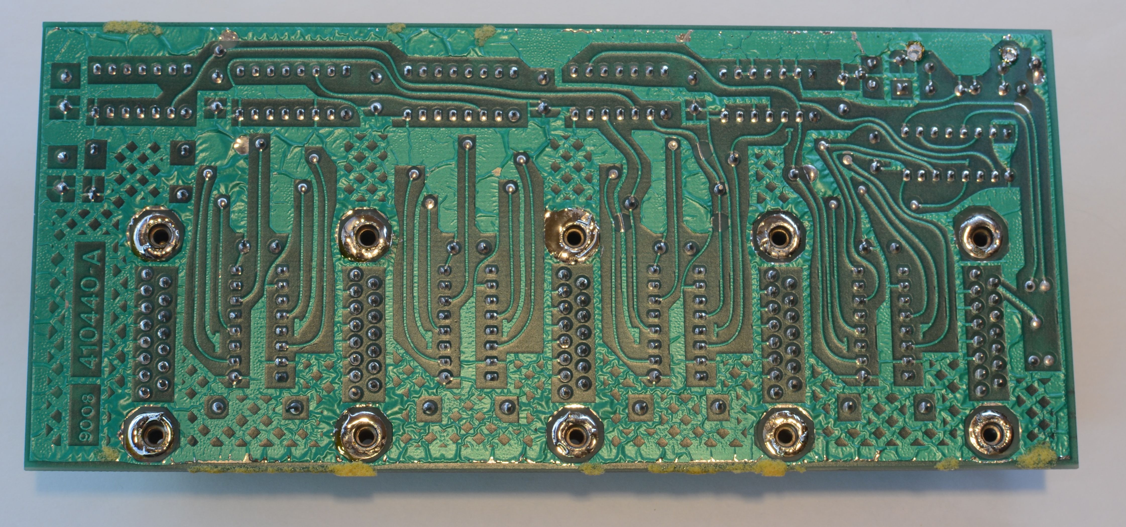
Image 182. Back side of the connector board
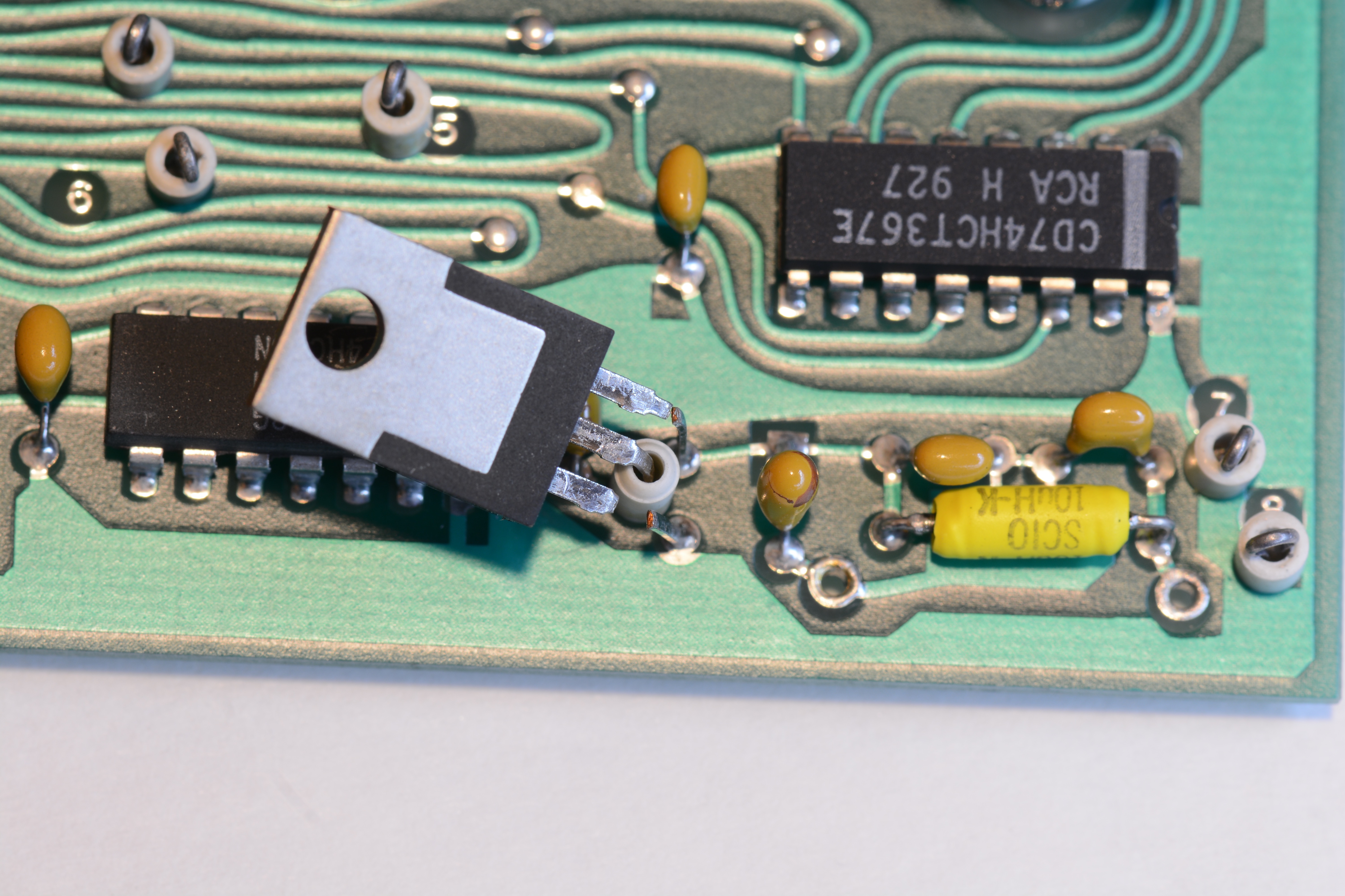
Image 183. Broken pins of the IC that needed repairs
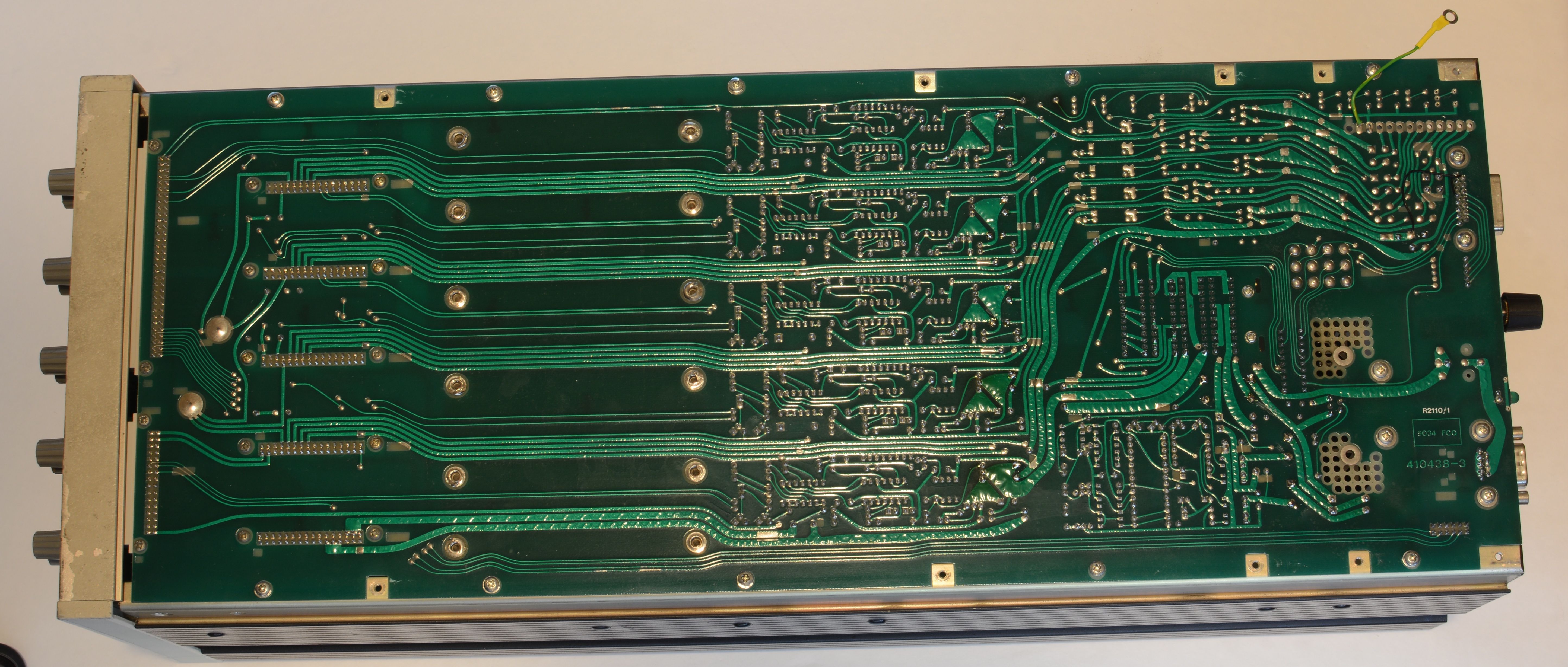
Image 184. Bottom with PCBA traces for backplane board
Battery compartment service and replacement with new cells
Image 185. Battery fuse protection board with DSub interconnets
Image 186. Red for positive terminals, black for negatives
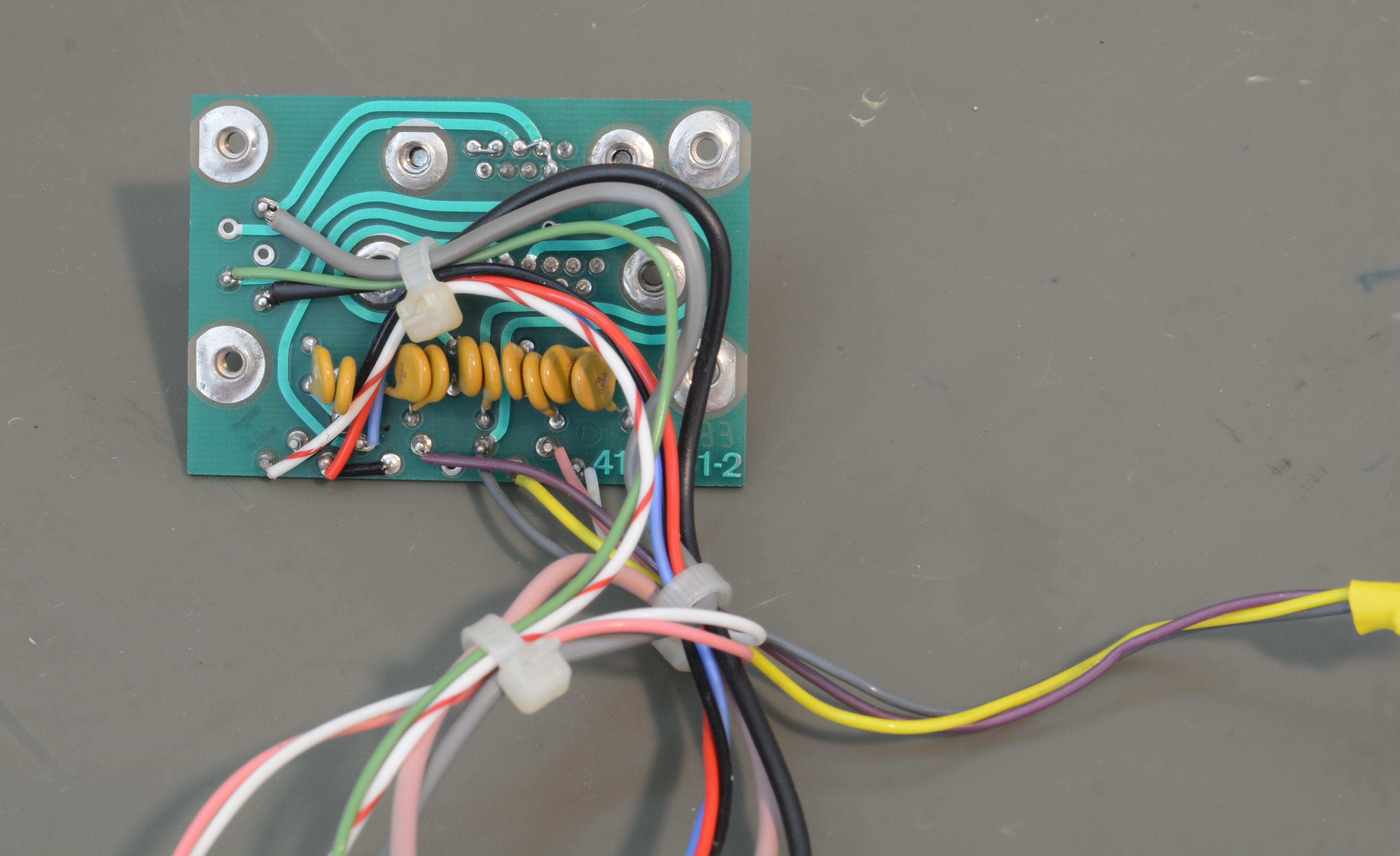
Image 187. Yellow disks are PTC fuses, 500 mA each
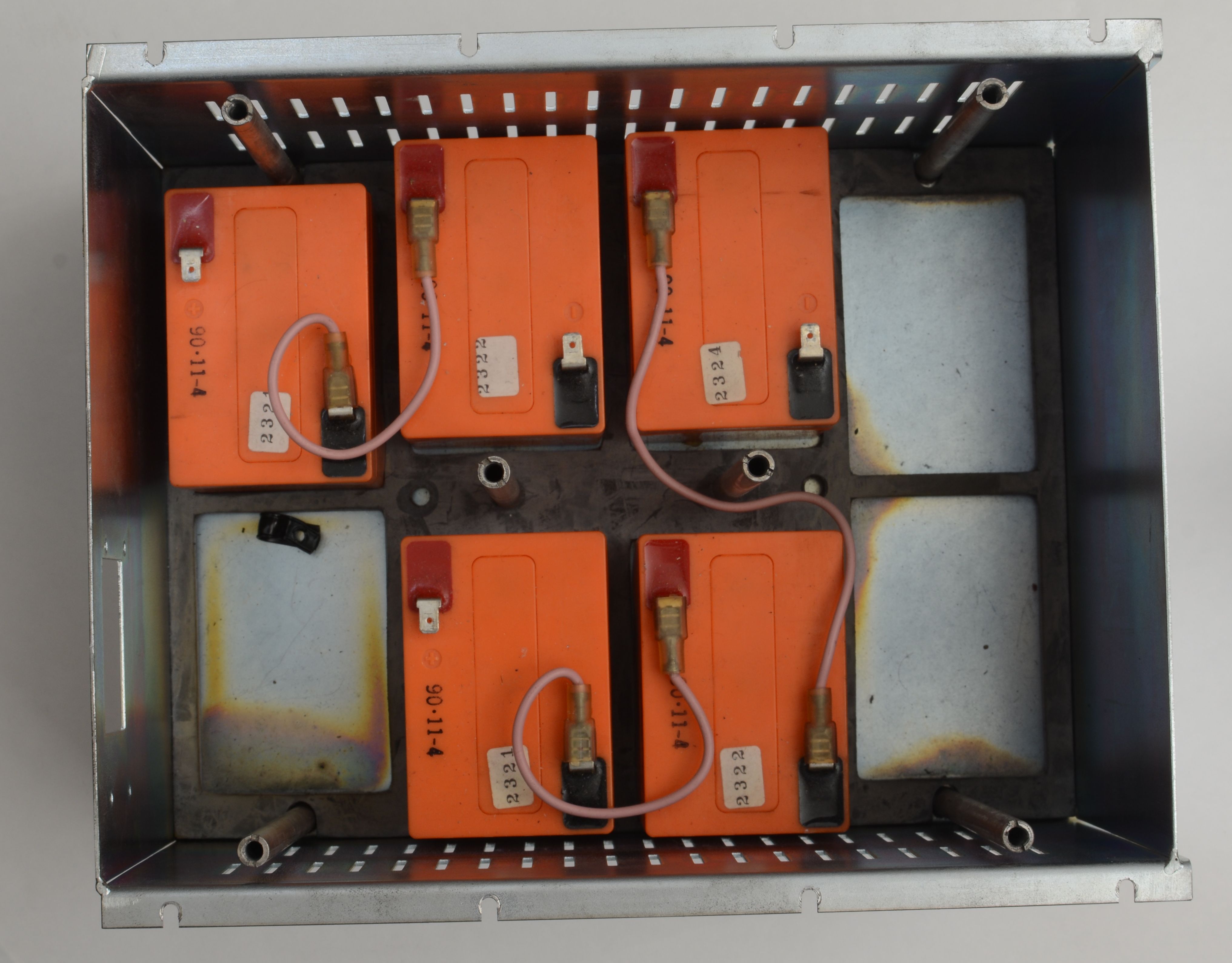
Image 188. Original battery cells and connections
Image 189. New foam for the bottom of the box
%(imgref)Image 190. Rubber gasket for battery %
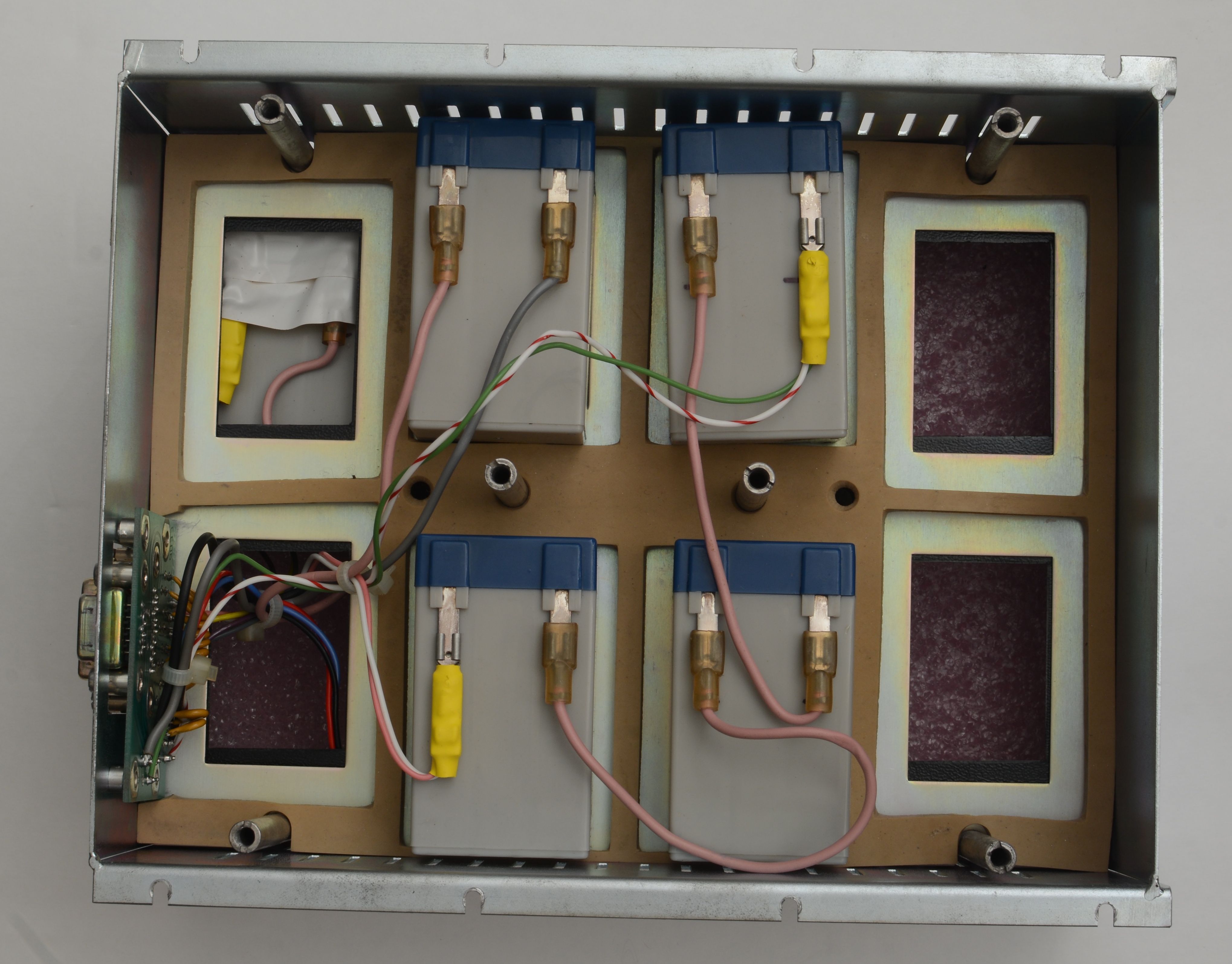
Image 191. Wiring for battery cells
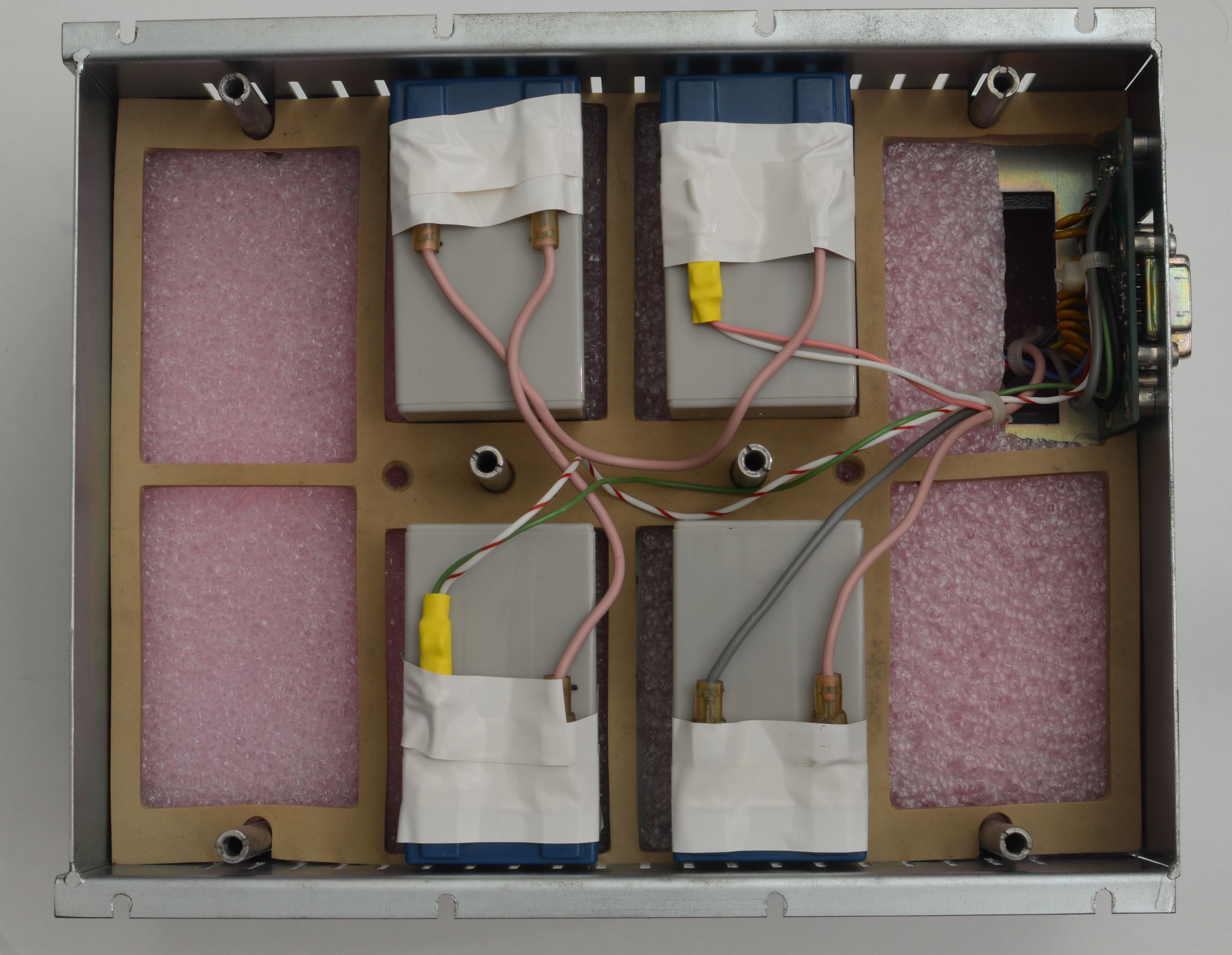
Image 192. Wiring for some battery cells
Image 193. Battery with top handle lid installed
Image 194. Battery unit ready to go
Long-term stability measurements for xDevs Datron 4910
TBD…
Summary and conclusion
Overall this Datron 4910 article and restoration were great fun and rewarding, with addition of four nice 10 V outputs at xDevs.com in-house voltage bank. Total expenses are listed below:
| Item | Qty | Cost per unit | Subtotal | Source |
|---|---|---|---|---|
| Datron 4910 reference, as is | 1 | $$$$ | $$$$ | secondary market |
| PowerSonic PS-621 battery, 6V 2Ah | 15 | 16.431 CAD | 246.47 CAD | BBMbattery.ca |
| Custom PTFE copper binding post | 20 | 5 CAD | 100 CAD | pip |
| LED RGB DIFFUSED T-1 3/4 T/H WP154A4SUREQBFZGW | 20 | 2.039 CAD | 40.78 CAD | Digikey 754-1492-ND |
| CAP ALUM 470 µF 20% 63V RADIAL TH EKY-630ELL471ML20S | 10 | 1.161 CAD | 11.61 CAD | Digikey 565-EKY-630ELL471ML20S-ND |
| CAP ALUM 330 µF 20% 50V RADIAL TH B41896C6337M000 | 10 | 1.347 CAD | 13.47 CAD | Digikey 495-6043-ND |
| RES 2 kΩ 5% 2W AXIAL PR02000202001JR500 | 10 | 0.345 CAD | 3.45 CAD | Digikey 56-PR02000202001JR500CT-ND |
| CAP TANT 2.2 µF 10% 50V RADIAL TAP225K050SRW | 20 | 0.953 CAD | 19.06 CAD | Digikey 478-8970-1-ND |
| CAP TANT 3.3 µF 20% 50V RADIAL TAP335M050CRW | 10 | 1.152 CAD | 11.52 CAD | Digikey 478-TAP335M050CRWCT-ND |
| CAP ALUM 1000 µF 20% 63V RADIAL UBY1J102MHL1TN | 10 | 2.682 CAD | 26.82 CAD | Digikey 493-UBY1J102MHL1TNCT-ND |
| CAP TANT 10 µF 10% 50V RADIAL TAP106K050CCS | 20 | 1.716 CAD | 34.32 CAD | Digikey 478-4172-ND |
| CAP ALUM 10 µF 20% 100V RADIAL TH REH0611100M100K | 10 | 0.206 CAD | 2.06 CAD | Digikey 478-REH0611100M100KCT-ND |
| MOSFET P-CH 60 V 280 mA TO92-3 ZVP2106A | 20 | 1.257 CAD | 25.14 CAD | Digikey ZVP2106A-ND |
| FUSE BRD MNT 1 A 125VAC/VDC AXIAL 0251001.MXL | 10 | 1.252 CAD | 12.52 CAD | Digikey F2313-ND |
| BUMPER SQU 0.81“L X 0.81“W BLK SJ-5023-BLACK | 36 | 0.431 CAD | 15.54 CAD | Digikey SJ-5023-BLACK-ND |
Total spent about 463 CAD and 60 hours on random evenings not including the Datron 4910 unit itself.
The author would like to express our appreciation to everyone contributed to this project. Special credits and mentions of great support:
- Alex R. who enabled this project revival
- Todd M. for patience and continuous support for keeping hobby metrology dream alive.
- John Pickering (Metron Designs) for giving us amazing Datron products and designs to explore.
- Ken Eckert for inspiration and upkeep of Datron/Wavetek manuals and information available
- Linear Technology for making top-level “Renez-Repus” reference available on the market and dedication to high levels of analog performance.
- David for support of metrology community with low thermal hardware and ideas
Discussion is very welcome thru comment section or at our own IRC chat server: xdevs.com (port 4808, channel: #xDevs.com) or at our own forum. If you have information and interesting ideas on Datron 4910 hardware modifications not mentioned or listed in this article, feel free to provide them and xDevs can test and add them with next article update. If you have own Datron 4910/4911/4912 in your lab, I’d love to hear about it and showcase your instrument performance here as well.
Projects like this are born from passion and a desire to share how things work. Education is the foundation of a healthy society - especially important in today's volatile world. xDevs began as a personal project notepad in Kherson, Ukraine back in 2008 and has grown with support of passionate readers just like you. There are no (and never will be) any ads, sponsors or shareholders behind xDevs.com, just a commitment to inspire and help learning. If you are in a position to help others like us, please consider supporting xDevs.com’s home-country Ukraine in its defense of freedom to speak, freedom to live in peace and freedom to choose their way. You can use official site to support Ukraine – United24 or Help99. Every cent counts.
Modified: April 1, 2026, 9:12 a.m.