- Introduction
- Disclaimer
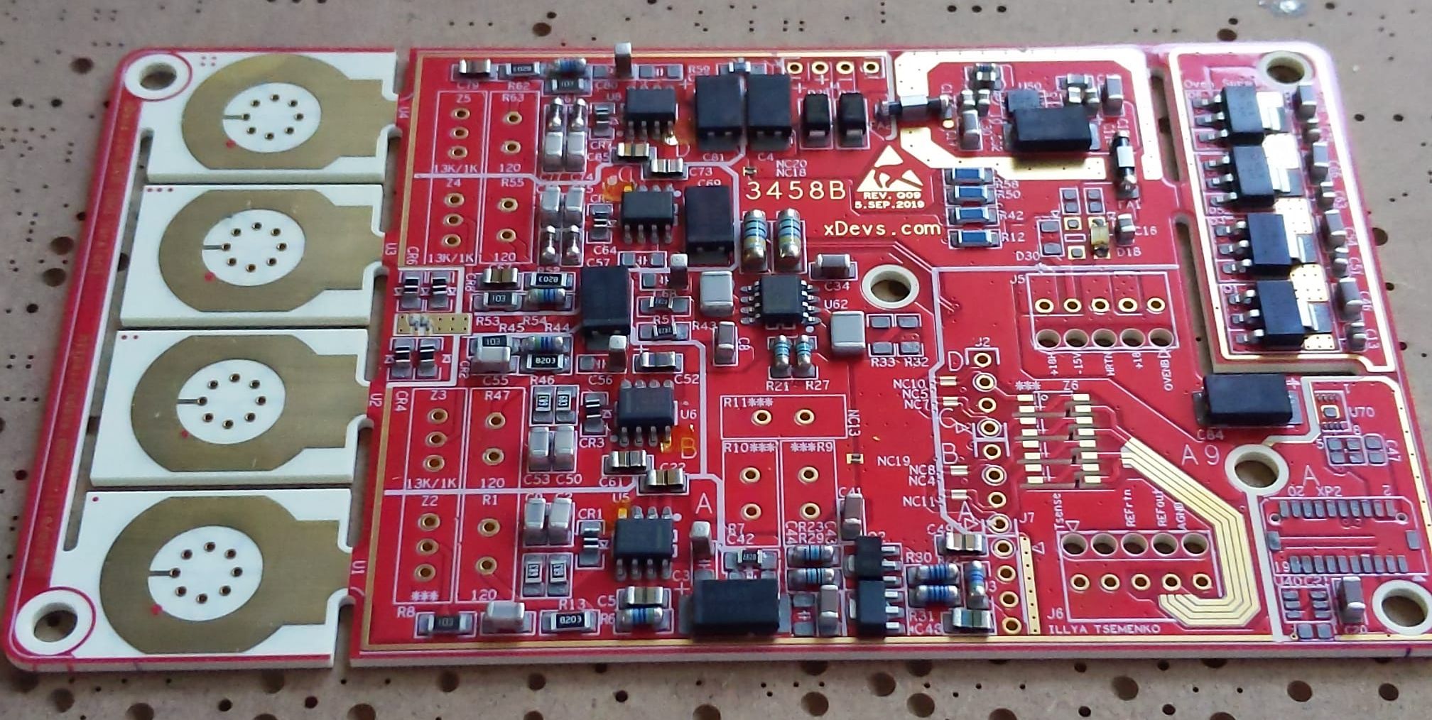
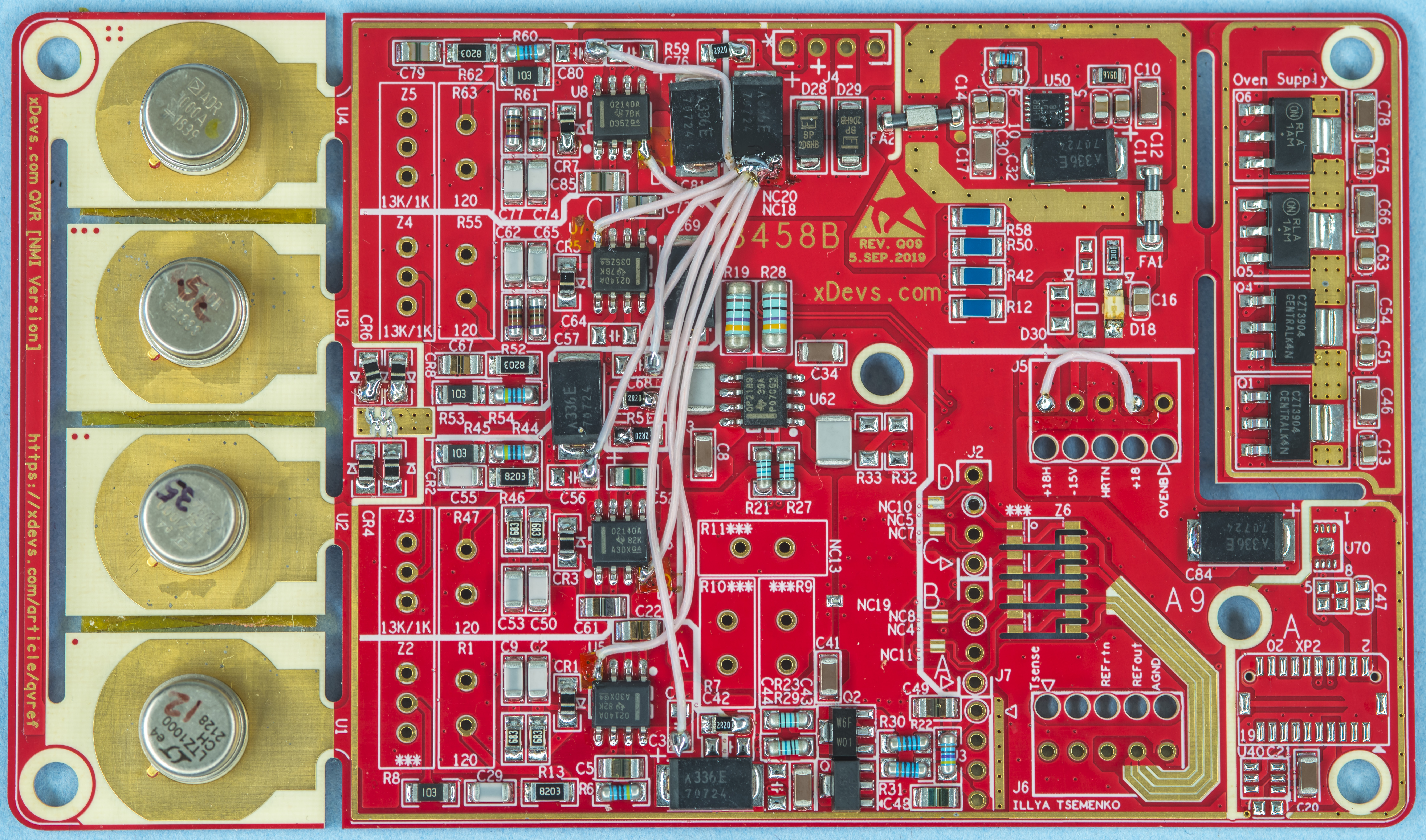
- SN0001 – Quad LTZ-chip module with 10V output
- SN0002 – Quad LTZ-chip module with 7.2V output
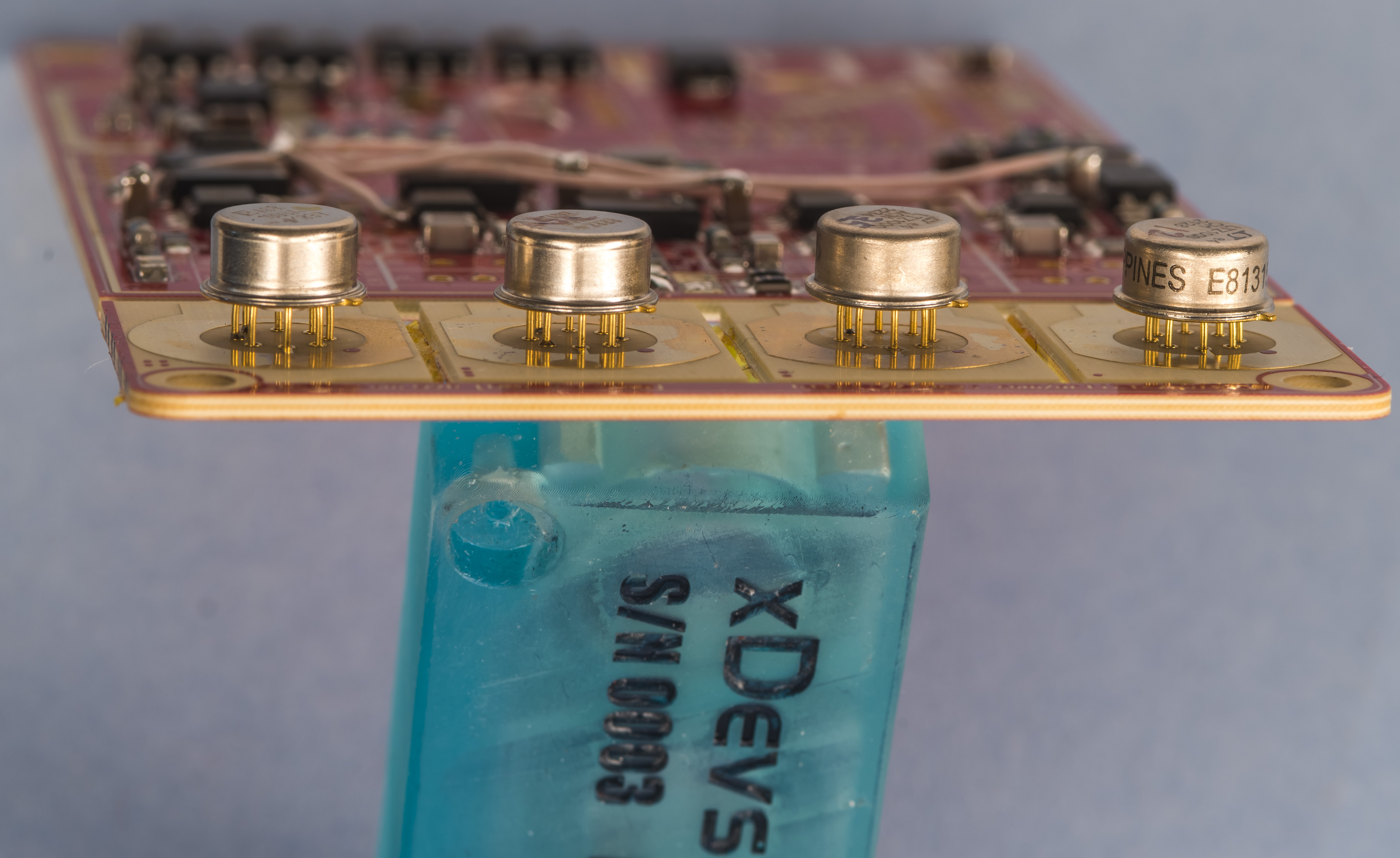
- SN0003 – Quad LTZ1000A low noise version
- SN0004 – Dual ADR-chip module with 10V output
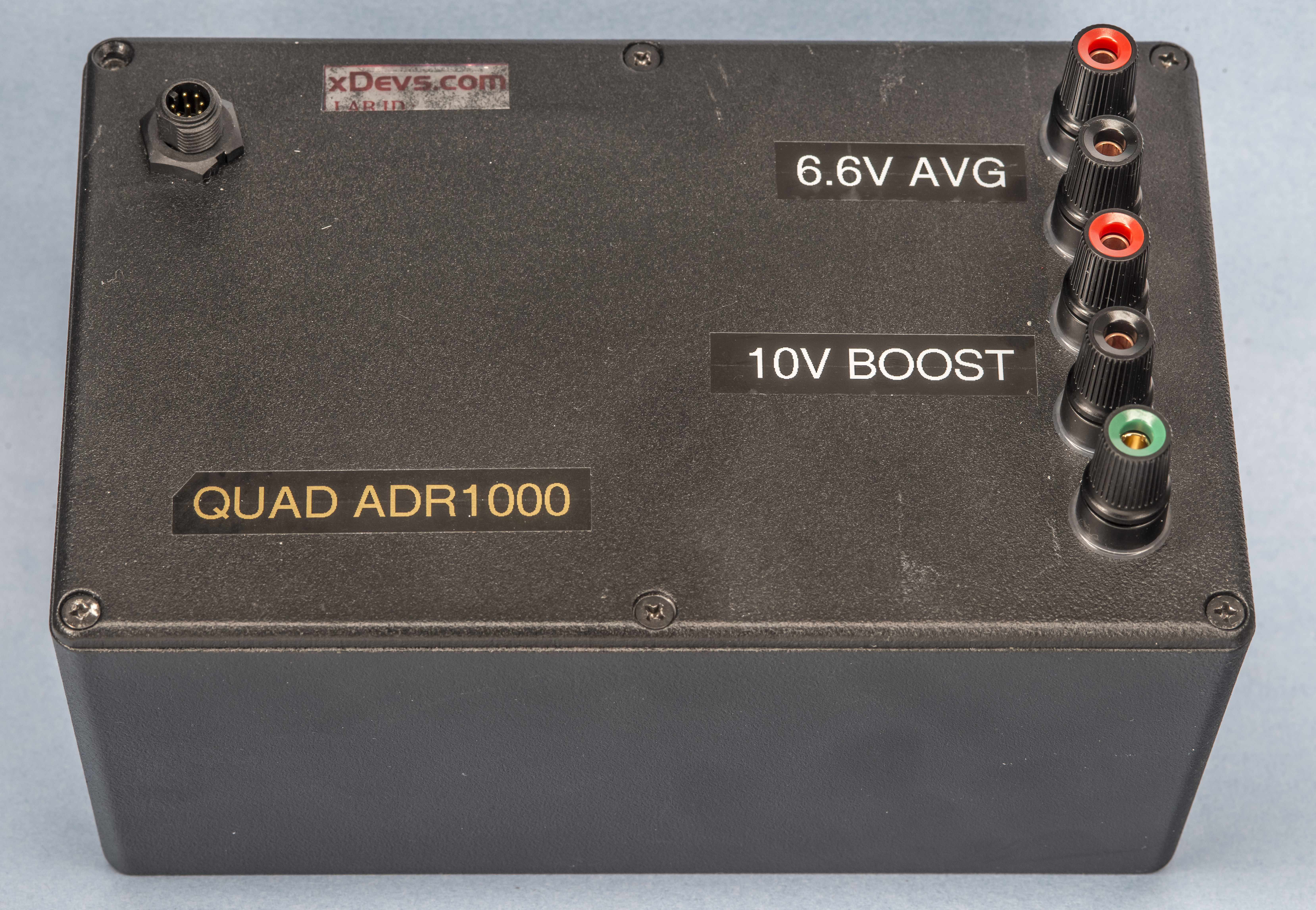
- SN0006 – Quad ADR-chip module with 10V output
- SN0005 – Quad ADR+LTZ comparison module with direct outputs
- SN0020 – Updated revision 2 QVR module with ADR1000
- SN0021 – Updated revision 2 QVR module with LTZ1000CH
- SN0022 – High power revision 2 QVR module with ADR1000
- Summary and conclusion
This is work in progress project, updates will be posted frequently.
Introduction
I’ve been always interested to see how practical it is to combine multiple best on the market zener references into averaged lower noise zener array bank. Practical example of such setup would be old Datron 4910 which has implemented averaged output from four LTZ1000-based cells. Four zener cores is a good balance between performance and cost, as theoretical reduction of the output noise follows square root of N law, where N is number of cells in the array. This means that ideally module with four zener chips will have half of the noise on the output voltage.
As for practical use case for such lower noise zener reference module – we can try it in HP 3458A DMM instead of original LTZ1000A A9 module and test if lowering noise for 7V reference helps with overall DMM noise performance. This is how Quad Voltage Reference “QVR” project came to life back in 2019 with first version. Design was revised and updated in May 2024 to improve performance and fix discovered hardware bugs.
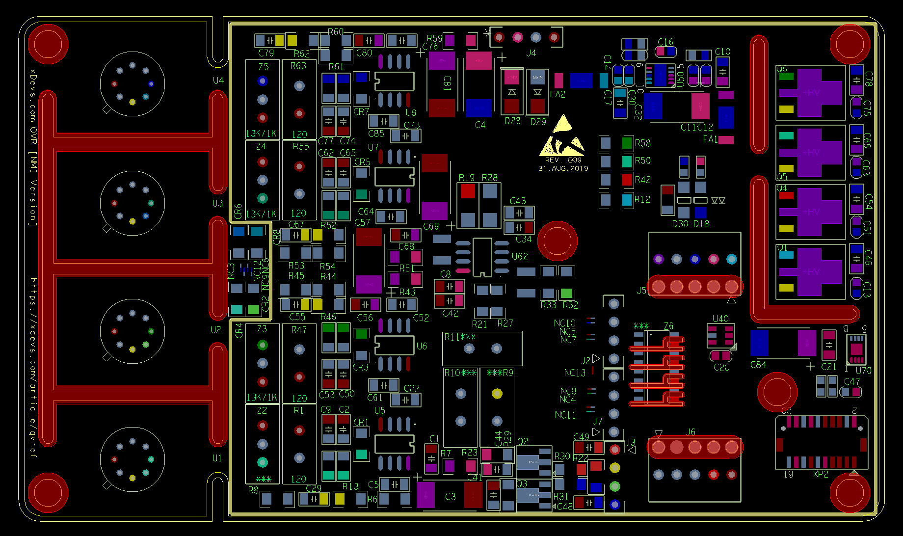
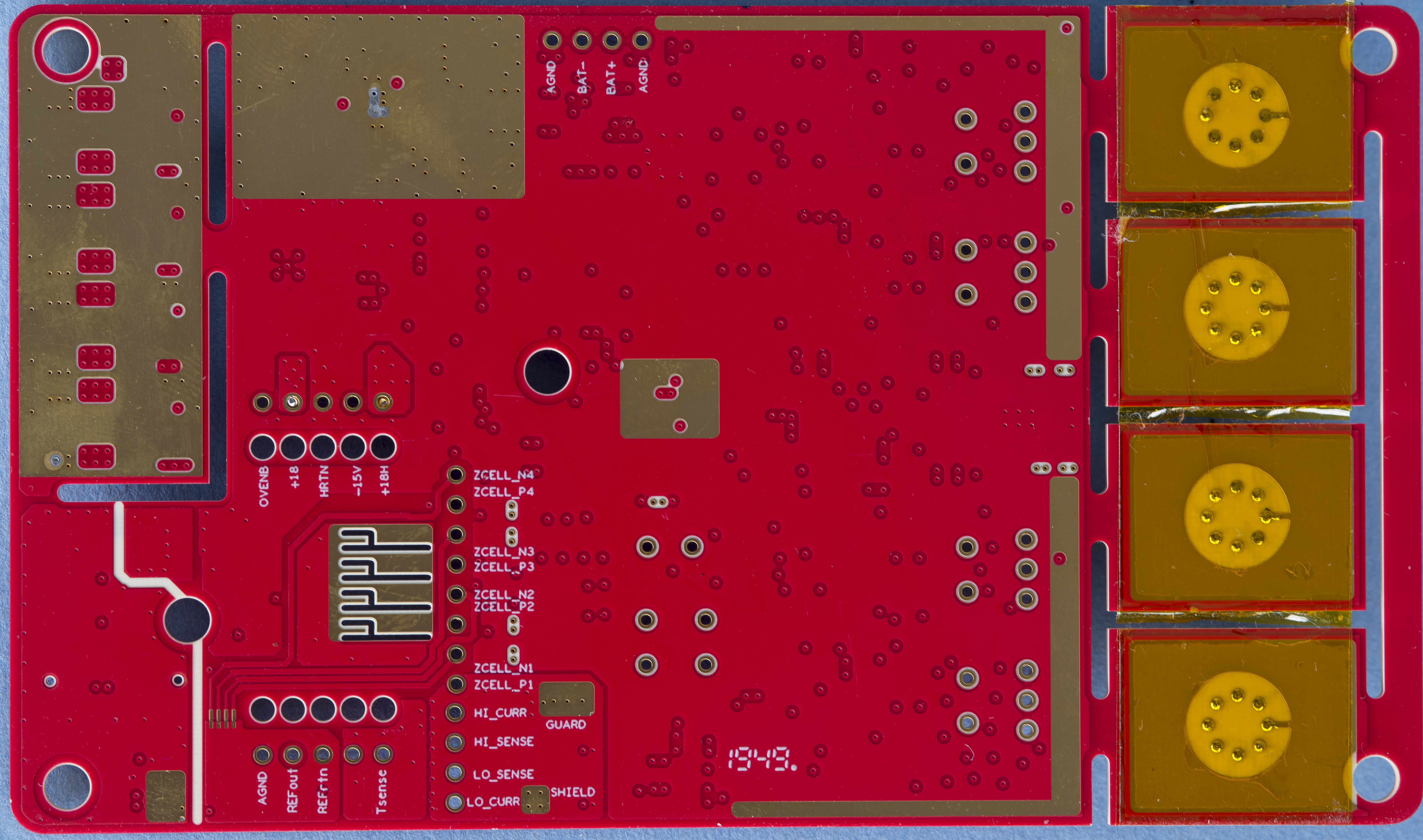
To have good separation between cells and ease of routing PCB Layout was done with six copper layers and Rogers RO4350 dielectric. Rogers dielectric is chosen for it’s environmental stability performance since the board assembly is targeted for tests in low pressure and low temperature environment.
This is NOT an open source project. xDevs.com QVR is a bit expensive as hobby device and specifically designed to our experiments and needs. If you still interested in it, feel free to contact us directly.
Disclaimer
Redistribution and use of this article, any part of it or any images or files referenced in it, in source and binary forms, with or without modification, are permitted provided that the following conditions are met:
- Redistributions of article must retain the above copyright notice, this list of conditions, link to this page (https://xdevs.com/article/qvref/) and the following disclaimer.
- Redistributions of files in binary form must reproduce the above copyright notice, this list of conditions, link to this page (https://xdevs.com/article/qvref/), and the following disclaimer in the documentation and/or other materials provided with the distribution, for example Readme file.
All information posted here is hosted just for education purposes and provided AS IS. In no event shall the author, xDevs.com site or any other 3rd party be liable for any special, direct, indirect, or consequential damages or any damages whatsoever resulting from loss of use, data or profits, whether in an action of contract, negligence or other tortuous action, arising out of or in connection with the use or performance of information published here.
If you are willing to contribute or add your experience regarding instrument repairs or provide extra information, you can do so following these simple instructions.
Certain commercial equipment, instruments, or materials are identified in this article to foster better understanding. Such identification does not imply recommendation or endorsement by the author or/and xDevs.com, nor does it imply that the materials or equipment identified are necessarily the best available for the purpose. Devices and components were not screened or conditioned prior to use in the electronic assembly, unless explicitly stated otherwise.
Hardware overview
Key aspects of this new multi-zener QVR zener reference are showcased in this chapter.
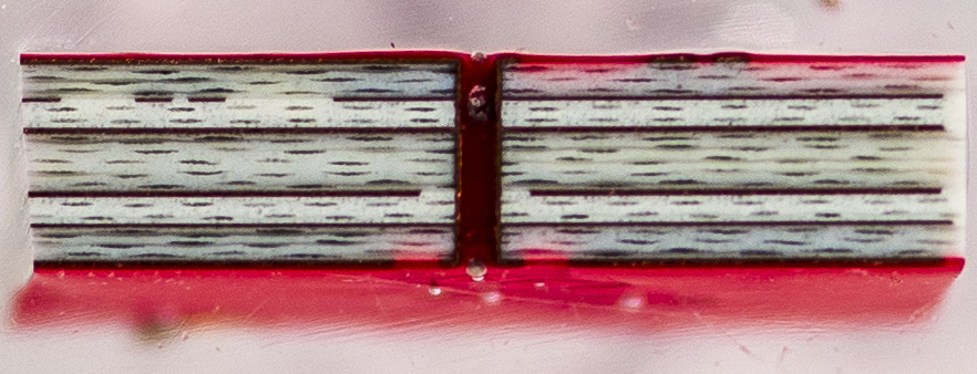
Cross-section of the PCB, overall thickness 1.6 mm.
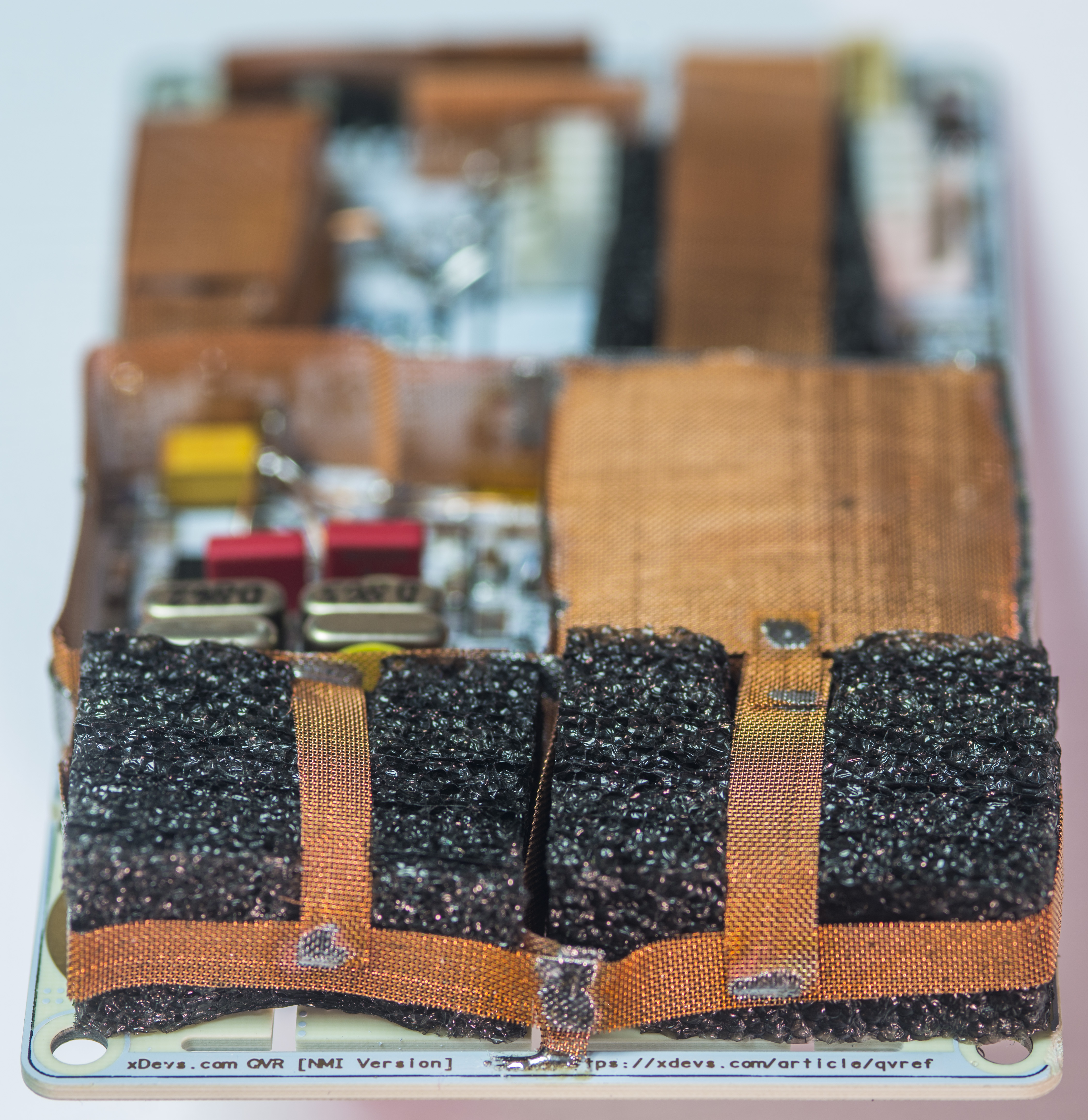
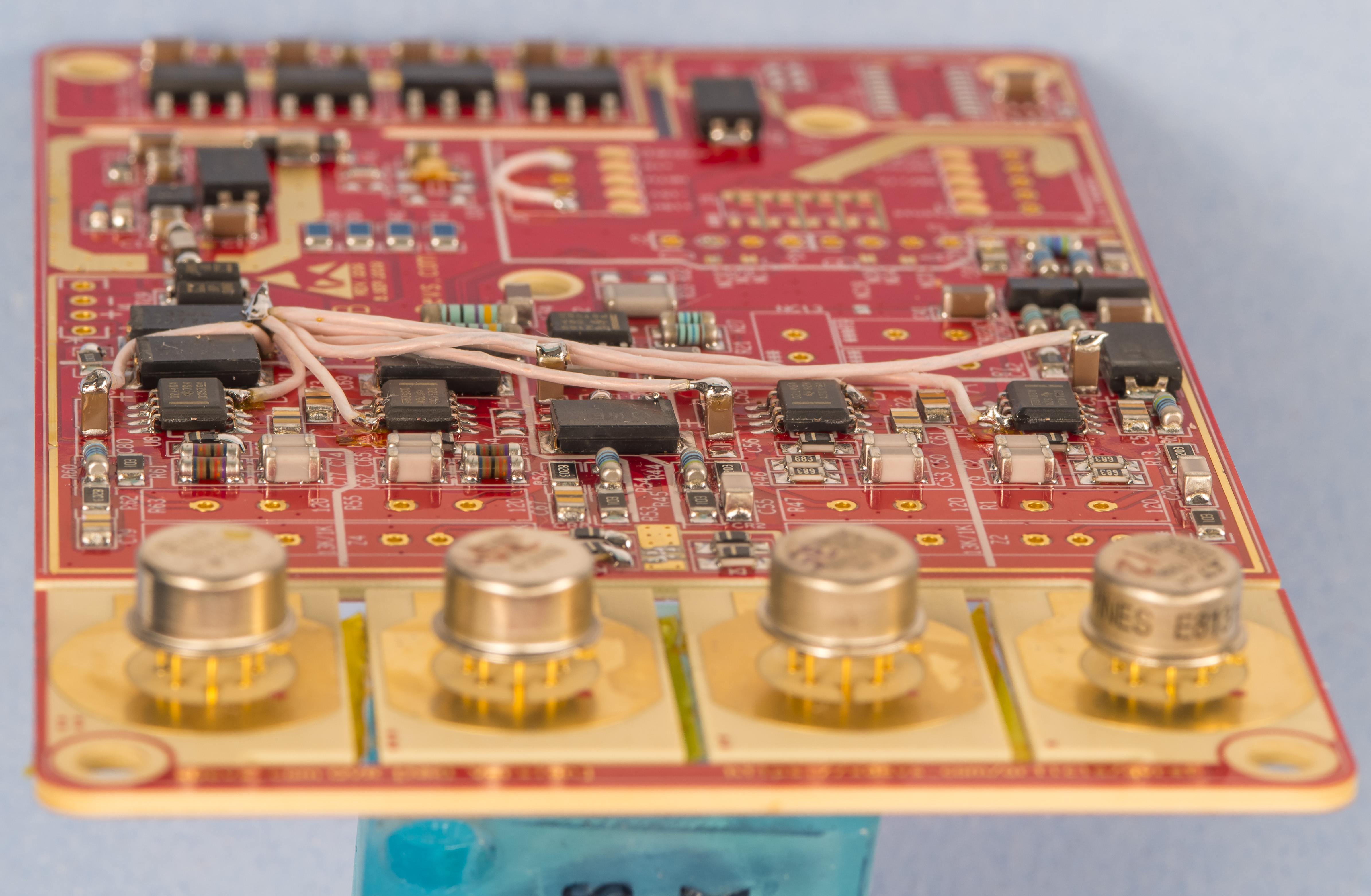
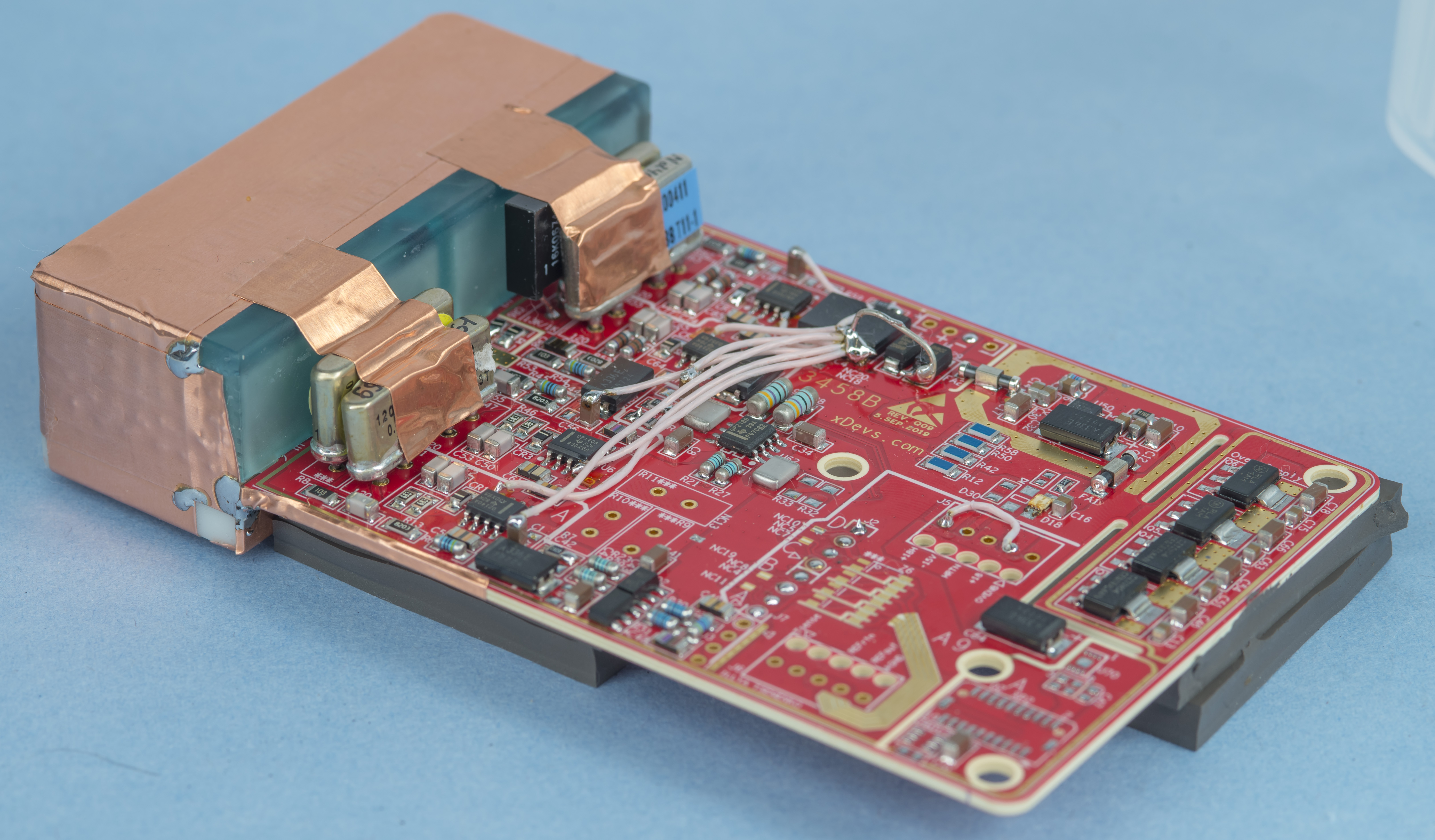
Module assembled with some additional shielding and air baffles to reduce low frequency noise from thermal variations around each of the LTZ1000A chips.
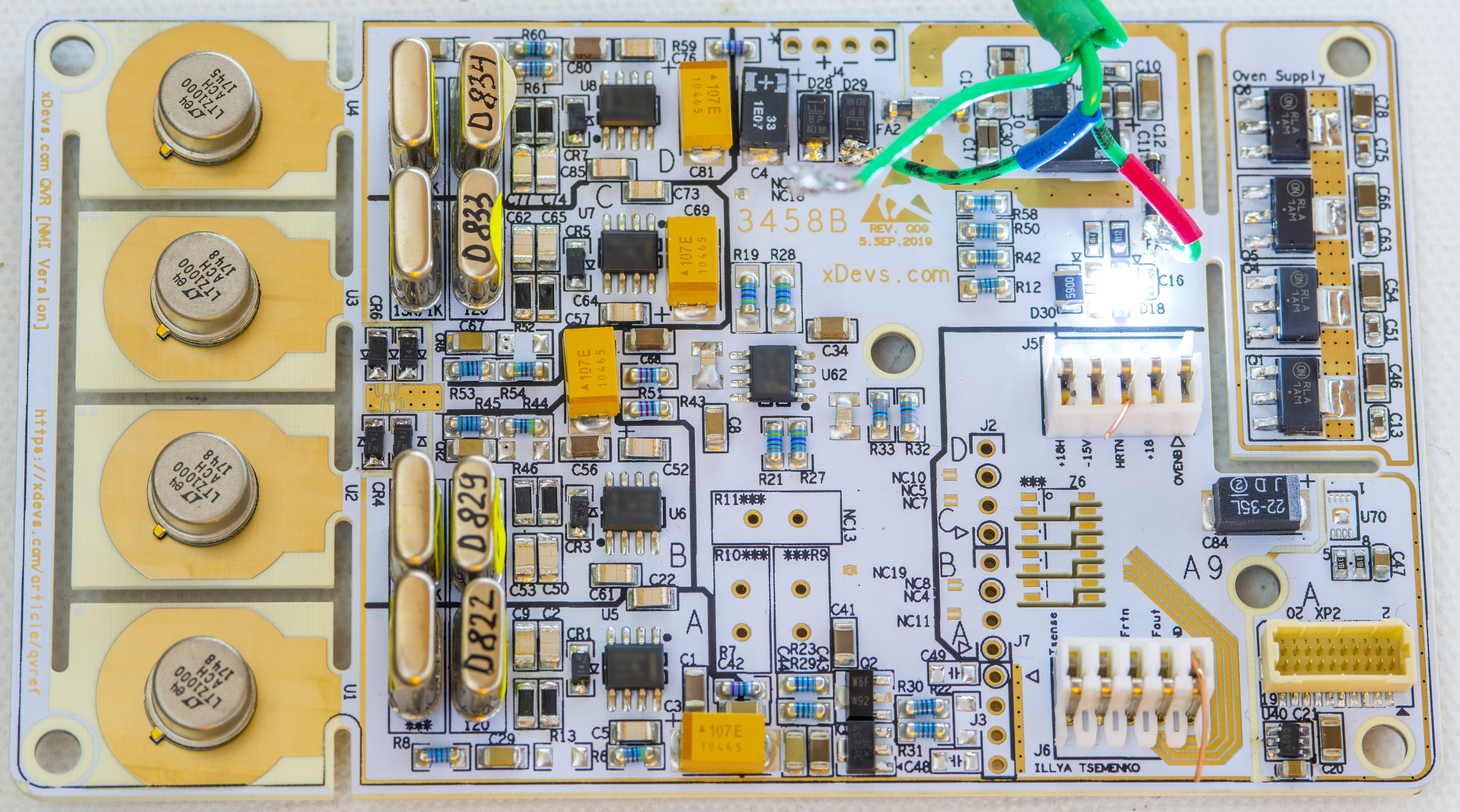
Module installed in Keysight 3458A DMM, replacing onboard A9 LTZ1000A-module

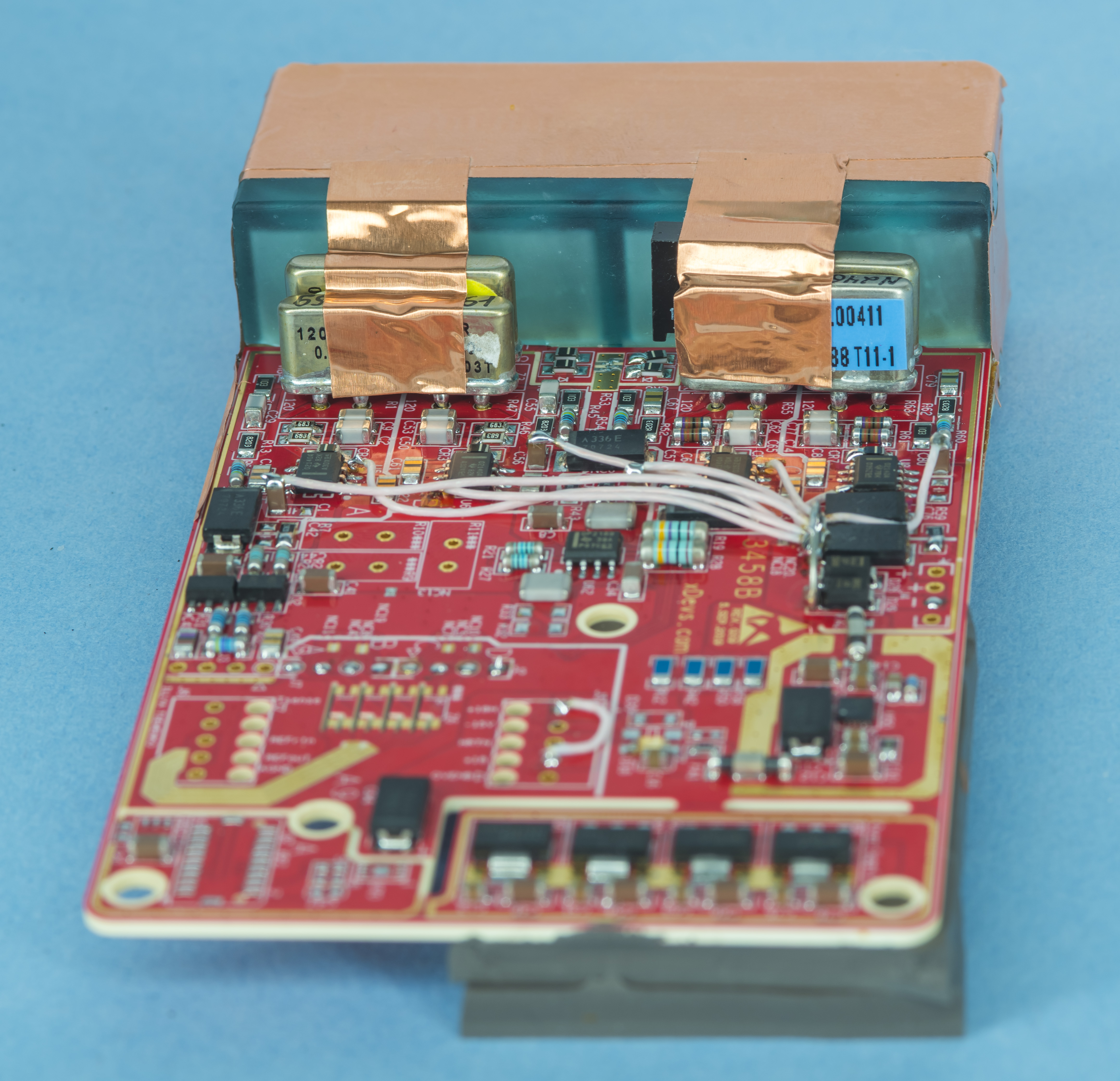
First module:
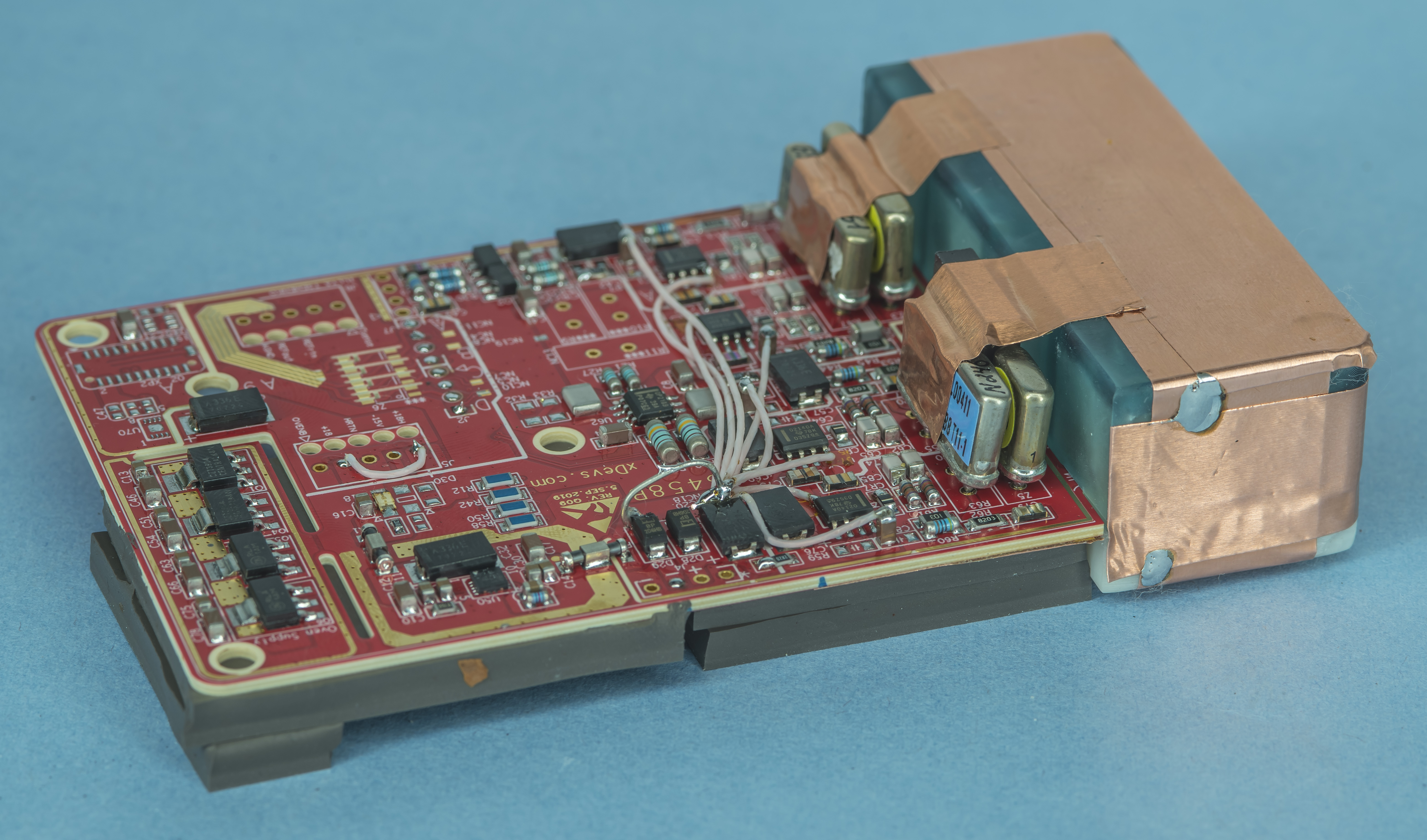
Second module:
Performance
Preliminary 0.1 – 10 Hz noise test results, room temperature.
Long-term stability.
QVR Unit #1 was mostly kept unpowered to evaluate deviation and instability of the quad LTZ1000A-based reference module. Measurements were handled at two different locations with international shipping of the unit with regular postal service (USPS at US end, EMS at NMI location).
Calibration reference value T23°C = 9.990901 VDC ±0.8 ppm , 10.SEP.2019
1st temperature sweep prior to shipping for NMI
2nd temperature sweep prior to shipping for NMI
Calibration result from NMI (Calibrated 3458A readout)
Calibration transfers on DC Zener bank array at NMI
Calibration reference value T23°C = 9.990904 VDC ±0.6 ppm , 17.JAN.2021
Then standard was returned and tested again, powered from Fluke 792X battery power pack.
Calibration reference value T17°C = 9.9909107 VDC ±0.6 ppm , 1.APR.2021
Calibration reference value T23°C = 9.9909107 VDC ±0.6 ppm , 1.APR.2021
Calibration reference value T30°C = 9.9909107 VDC ±0.6 ppm , 1.APR.2021
Calibration reference value T45°C = 9.9909107 VDC ±0.6 ppm , 1.APR.2021
Datalog with triple 3458A, in thermal chamber
Second prototype batch with ADR1000AHZ superzeners
SN0003 – Quad LTZ1000A low noise version
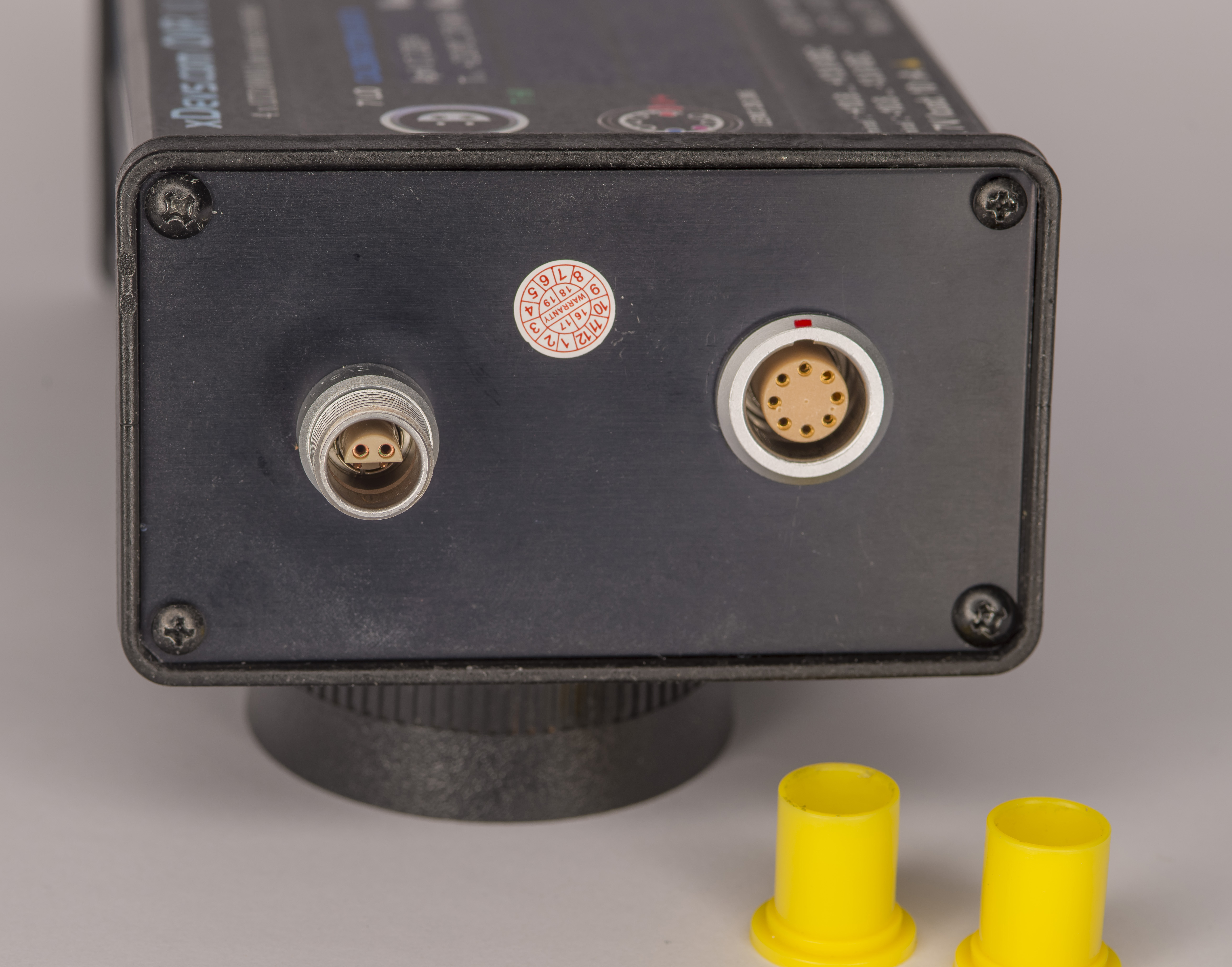
This QVR module is built with four LTZ1000ACH cells aged for 4 years with main goal on providing low noise output. It is trimmed for output just +2.1 µV/V above nominal 10 V and has two DC voltage outputs provided to user by LEMO 1B.EVP connector. 10 V output is routed from active discrete PNP/NPN stage from gain OPA2189 amplifier. Output resistance is less than 2 Ω. Second averaged +7.1 V output is provided on same connector. It is unbuffered and taken directly from the passive resistor averaging network. Output resistance for +7.1 V output is about 2 kΩ and it cannot drive any load. Small 10 nA current loading may cause error close to 0.1 µV/V for this output.
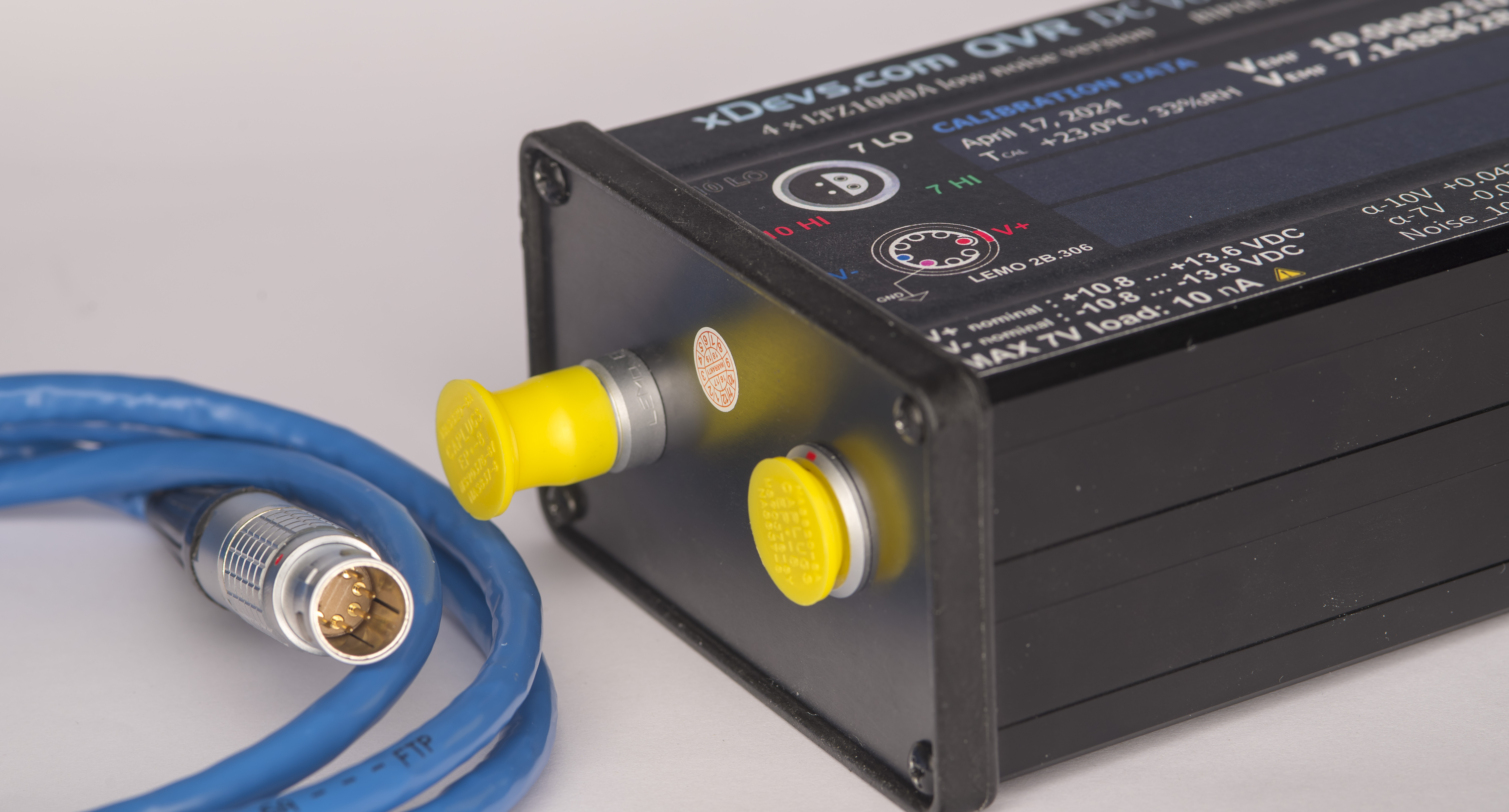
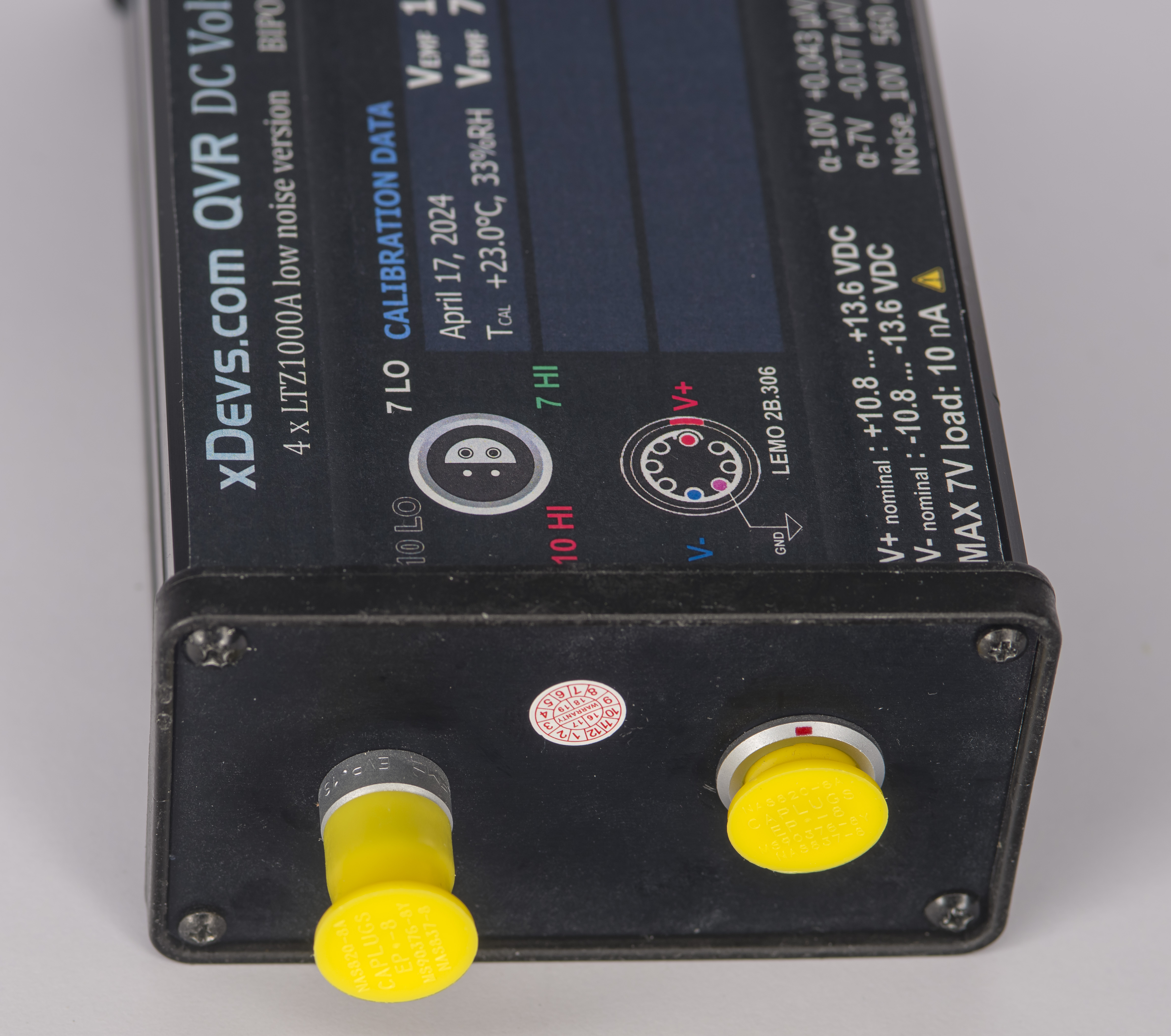
Kit is supplied with 8-conductor cable terminated with 2B.308 connector. This connector provide power to the reference. For proper operation it is best to supply at least +11 and -11 V DC to the module. Pinout for the connector listed in table below:
| LEMO 2B.308 connector pin | Purpose | Rated input | Nominal supply current |
|---|---|---|---|
| Pin 1 | Positive voltage supply | +10.8 to +13.6 V | 0.26 A after warm-up, 0.4 A cold |
| Pin 5 | Negative voltage supply | -10.8 to -13.6 V | 0.005 A after warm-up, 0.01 A cold |
| Pin 6 | Ground/return pin | Reference zero |
Reference has no adjustable elements or user controls and operational after 6 hour warm-up time.
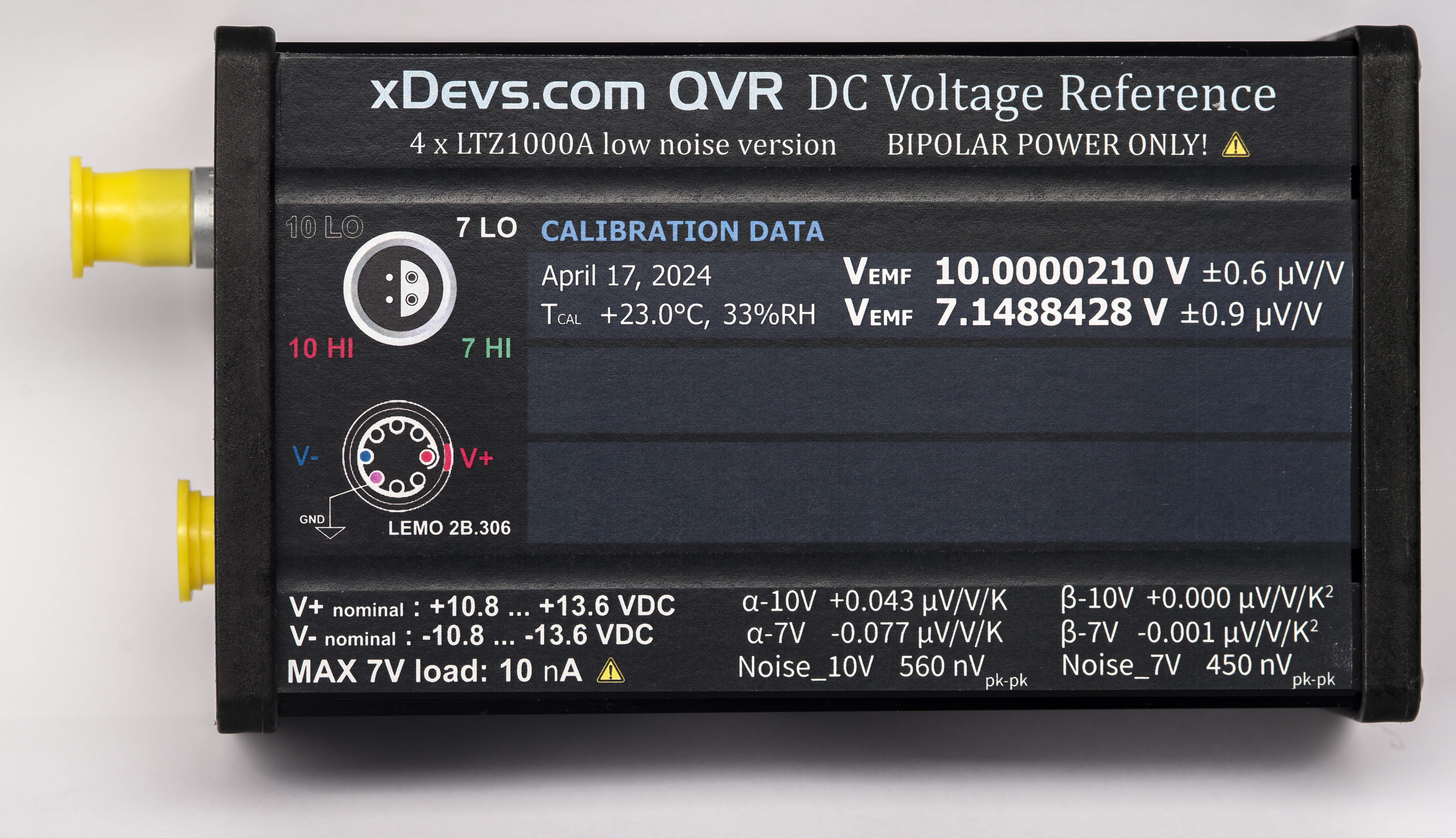
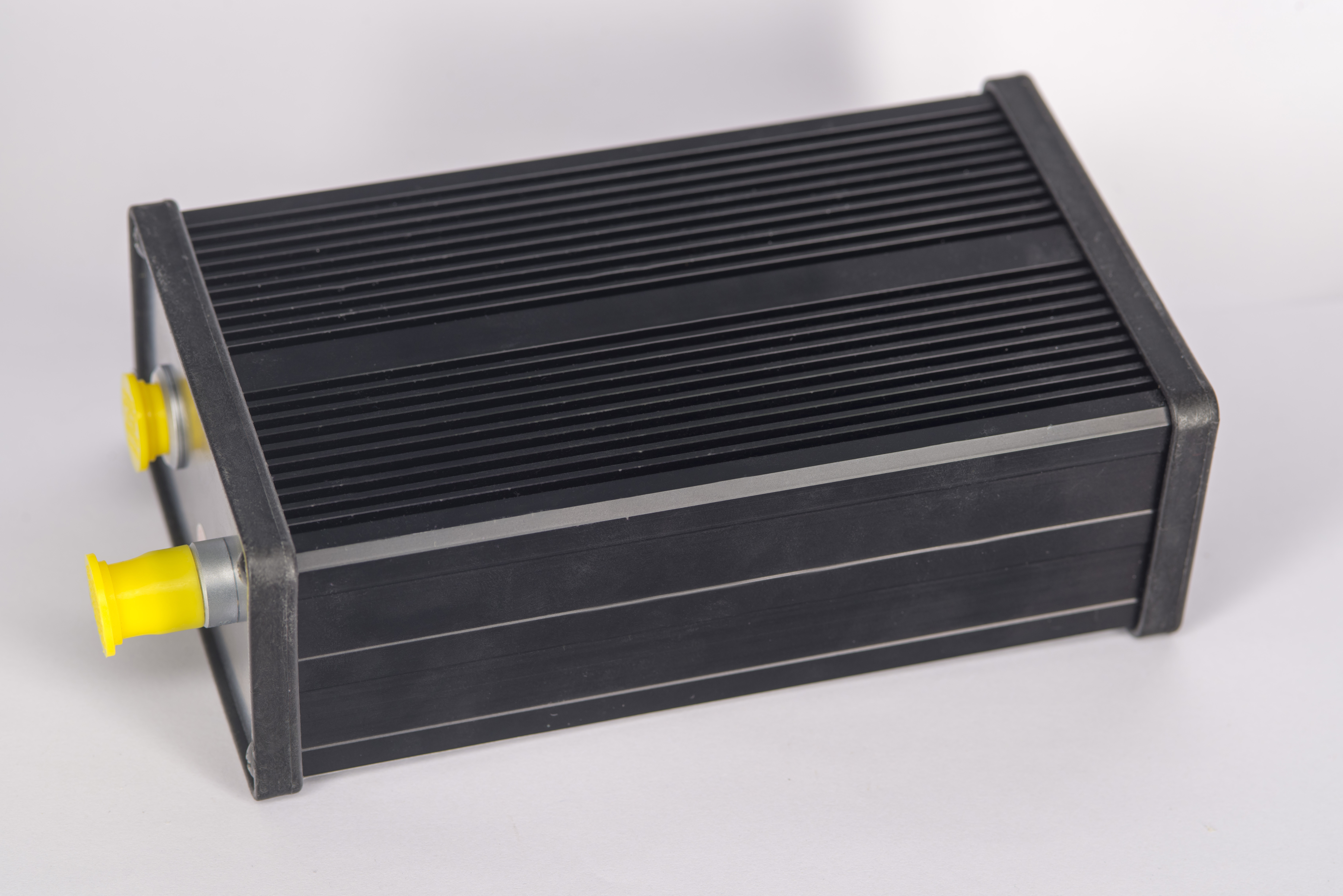
Bottom side of aluminum extruded enclosure has heatsink fins for additional dissipation of the heat from the reference. Time delay for inner temperature is about 2 hours.
All key performance parameters and current calibration data is added on the enclosure label for the ease of use.
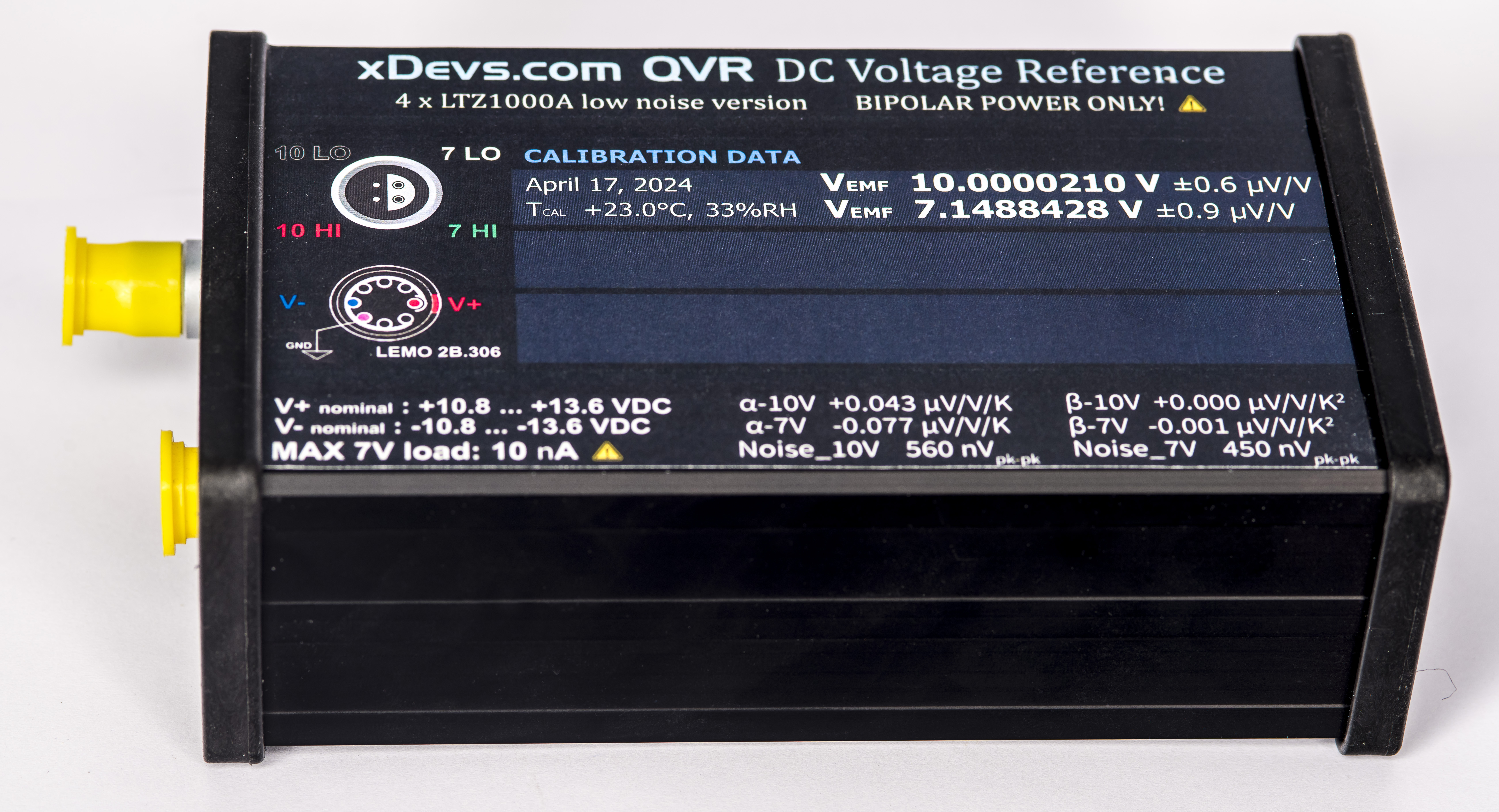
For shipping connectors are protected with plastic caps.
LEMO 1S.EVP connector is identical to one used in Keithley 2182/2182A and HP/Agilent/Keysight 34420A nanovoltmeters. If standard nanovoltmeter cable connected to this QVR module signals mapping for wires is as listed in table below.
| nV cable wire | Purpose |
|---|---|
| Red wire | Positive output for +10 V |
| Black wire | Negative return for +10 V |
| Green wire | Positive output for averaged passive +7.1 V |
| White wire | Negative return for averaged passive +7.1 V |
Do not source or sink current into averaged passive +7.1 V to avoid risk of damaging input amplifier or resistor network.
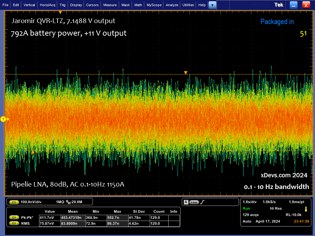
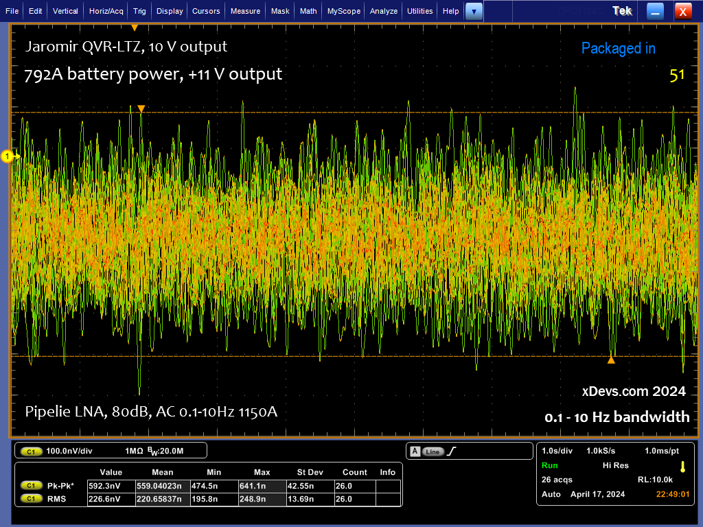
Calibration results for 17 April, 2024, battery powered from Fluke 792A.
Calculated polyfit for 7V output = -3.73278597E-09×2 – 3.81348455E-07x + 7.14885389E+00
Calculated polyfit for 10V output = 1.61494518E-09×2 + 3.57968196E-07x + 1.00000095E+01
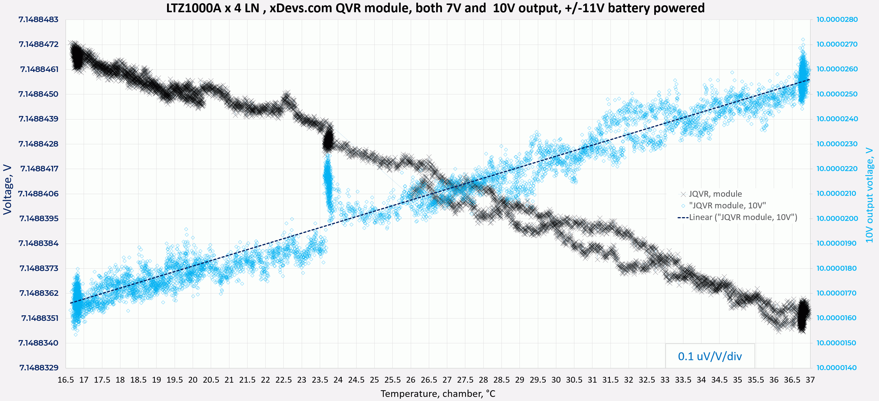
With standard analysis for tempco with reference +23.0 °C we now can obtain
+7 V TCR α -0.077 µV/V/K, β -0.001 µV/V/K2, Tzero = -51.1 °C
+10 V TCR α +0.043 µV/V/K, β 0.0002 µV/V/K2, Tzero = -110.8 °C
Absolute output calibration from zener array bank determined EMF at 10.00002096 V ±0.6 µV/V and 7.1488428 V ±0.9 µV/V with +23.0 °C temperature. Warm-up time from cold state is 6 hours.
This reference require high-isolation bipolar power supply or battery power. Error due to ground currents on standard linear power supply (Keysight E36312A) was measured around +0.8 µV/V.
Noise measurement for 7 V output in 0.1 Hz – 10 Hz bandwidth, result about 450 nV peak to peak. This is just ±0.032 µV/V relative to 7.15 V output.
Noise measurement for 10 V output in 0.1 Hz – 10 Hz bandwidth, result about 560 nV peak to peak. This is just ±0.028 µV/V relative to 10 V output. For comparison modern Fluke 732C DC reference generate twice larger noise in this bandwidth for its 10V output.
SN0004 – Dual ADR-chip module with 10V output
| Parameter | Property | Note |
|---|---|---|
| Zener | C: ADR1000AHZ, A: ADR1000AHZ | unaged new chips, 6mm mount gap to PCB, 13mm total top Z height |
| Temp setpoint | C: 11500:1000 Ω VHD200, A: 13000:1000 Ω VHD200 | C:new chip, A: network S/N 8 |
| IZ setpoint | Both 80 Ω VHP202ZT | new chips, random run, not selected |
| BiasR | 4 × 62 kΩ MELF0204 5 ppm/K | |
| Opamp | OPA2140 for zener cells, ADA4522-2 for output stage | |
| Output scale | RDIV VHD200 10000:5105 Ω | R11:R9 position |
| TC trim oven | C: TBD, A: TBD | |
| Capacitors | C: 100nF C0G, A: 100nF Film | |
| Power | Onboard LT3045 | +12VDC output voltage point |
| Output cap | None | |
| Z6 network | TBD | |
| EEPROM | None |

Noise performance of SN0004 unit
Here are noise measurement results with battery-operated QVR module and battery operated 80 dB 0.1-10Hz AC coupled LNA.
C Cell : RAW output noise (+6.62 VDC from Zener core) measurement in 0.1 – 10 Hz bandwidth :
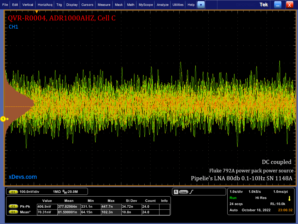
Average value is 377 nV peak to peak, which is good for a single ADR zener. Measurement standard deviation is 34 nVptp.
A Cell : RAW output noise (+6.62 VDC from Zener core) measurement in 0.1 – 10 Hz bandwidth :
This cell operates at higher oven temperature around +75 °C.
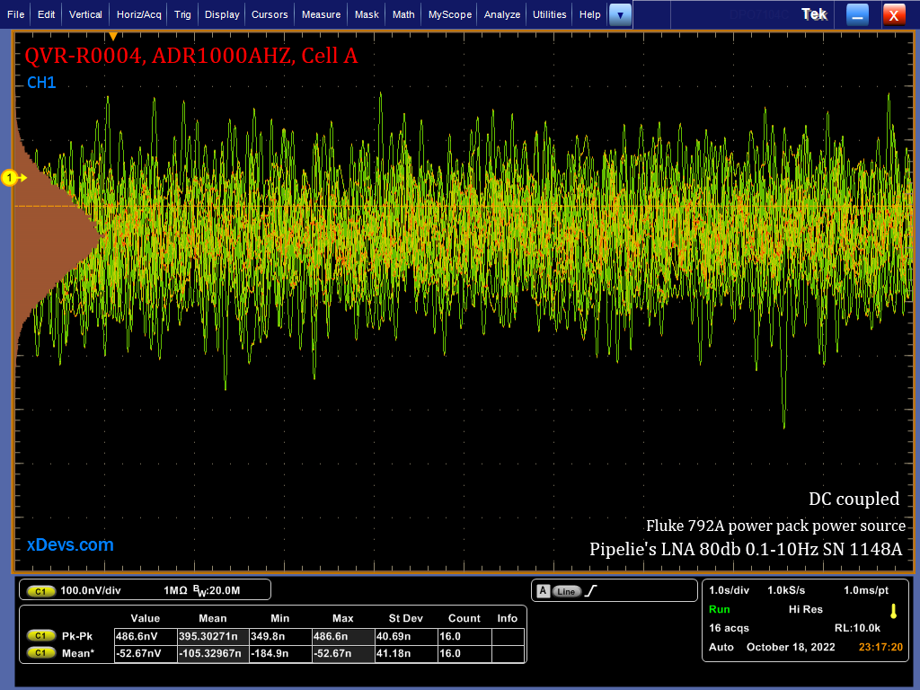
Average value is 395 nV peak to peak, which is good for a single ADR zener. Measurement standard deviation is 41 nVptp.
Now A+C combined cells with 250||250 foil resistors. This is combined RAW output noise (+6.62 VDC from two zener cores) measurement in 0.1 – 10 Hz bandwidth.
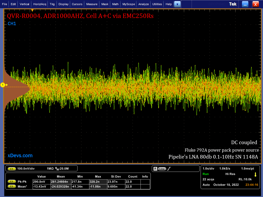
Average value is 281 nV peak to peak, which is promising result with just two ADR zeners. Measurement standard deviation is 24 nVptp. This is pretty close to quad LTZ1000A-based QVR results, which was ~248 nV peak to peak with same measurement setup.
Noise floor of this noise measurement setup is around 100 nV peak to peak.
This quad ADR1000 module was retrimmed for temperature coefficient below 0.05 µV/V/K.
And boxed unit:
Low thermal TBP3 posts were used for best 5-way connection interface to the QVR reference module.
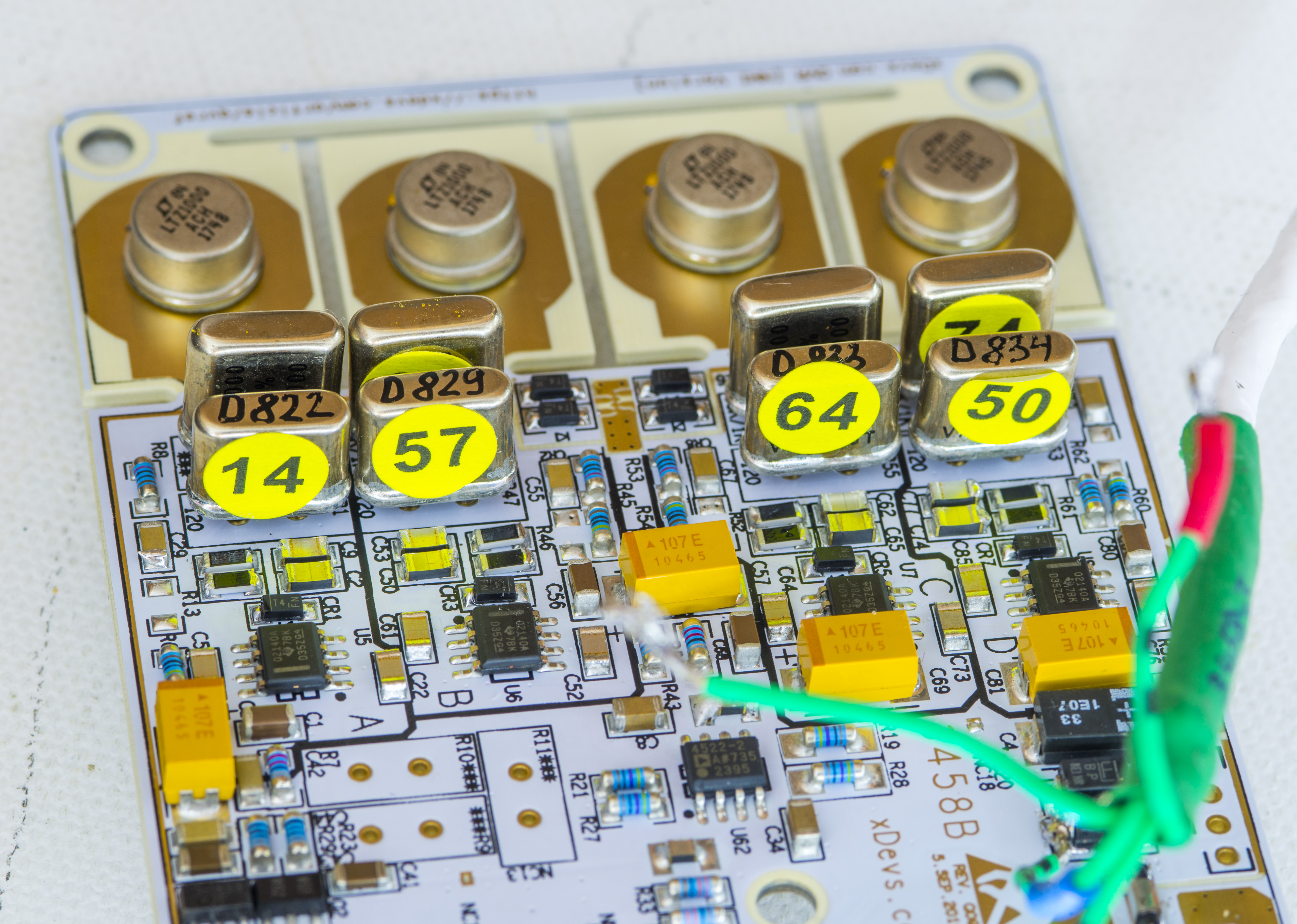
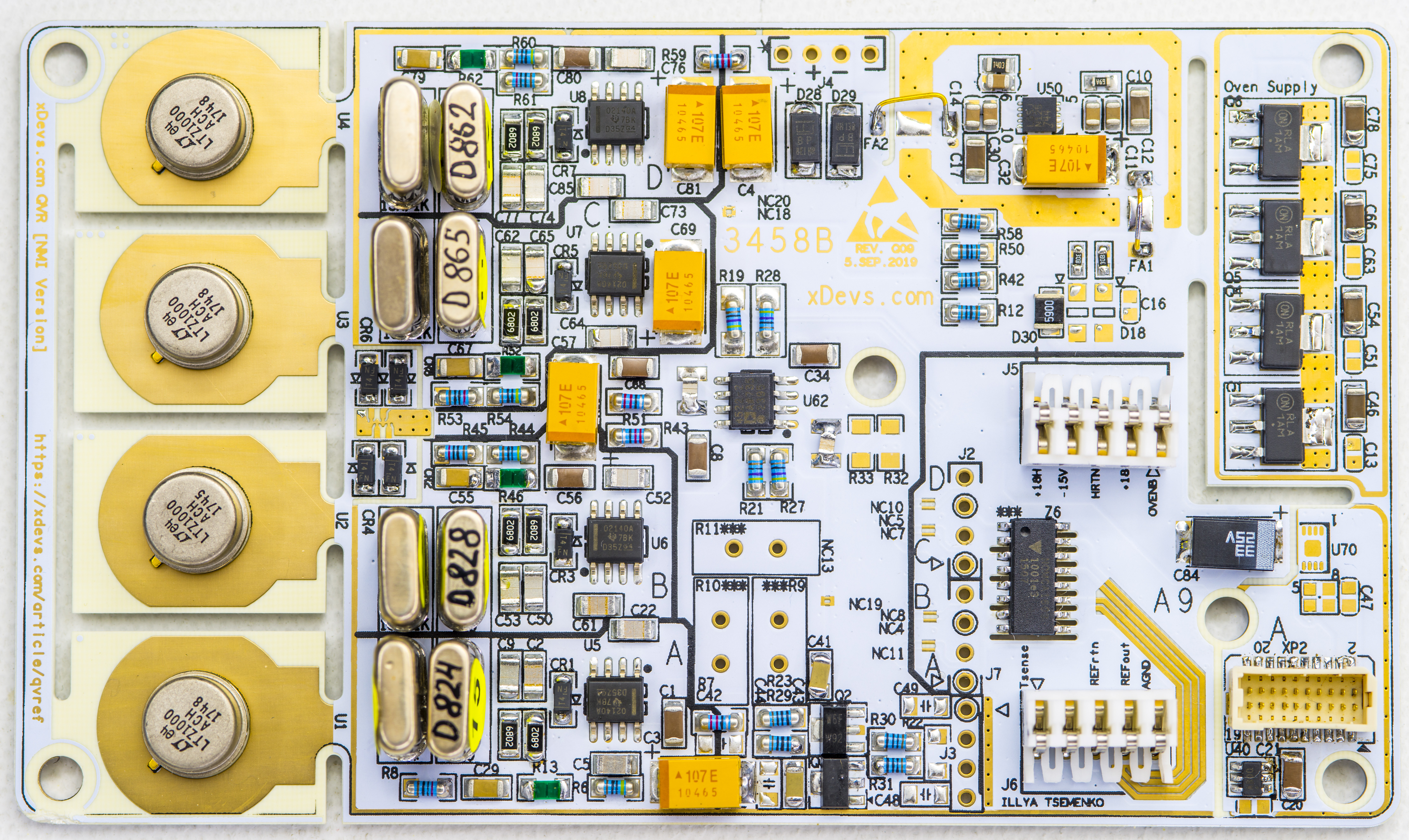
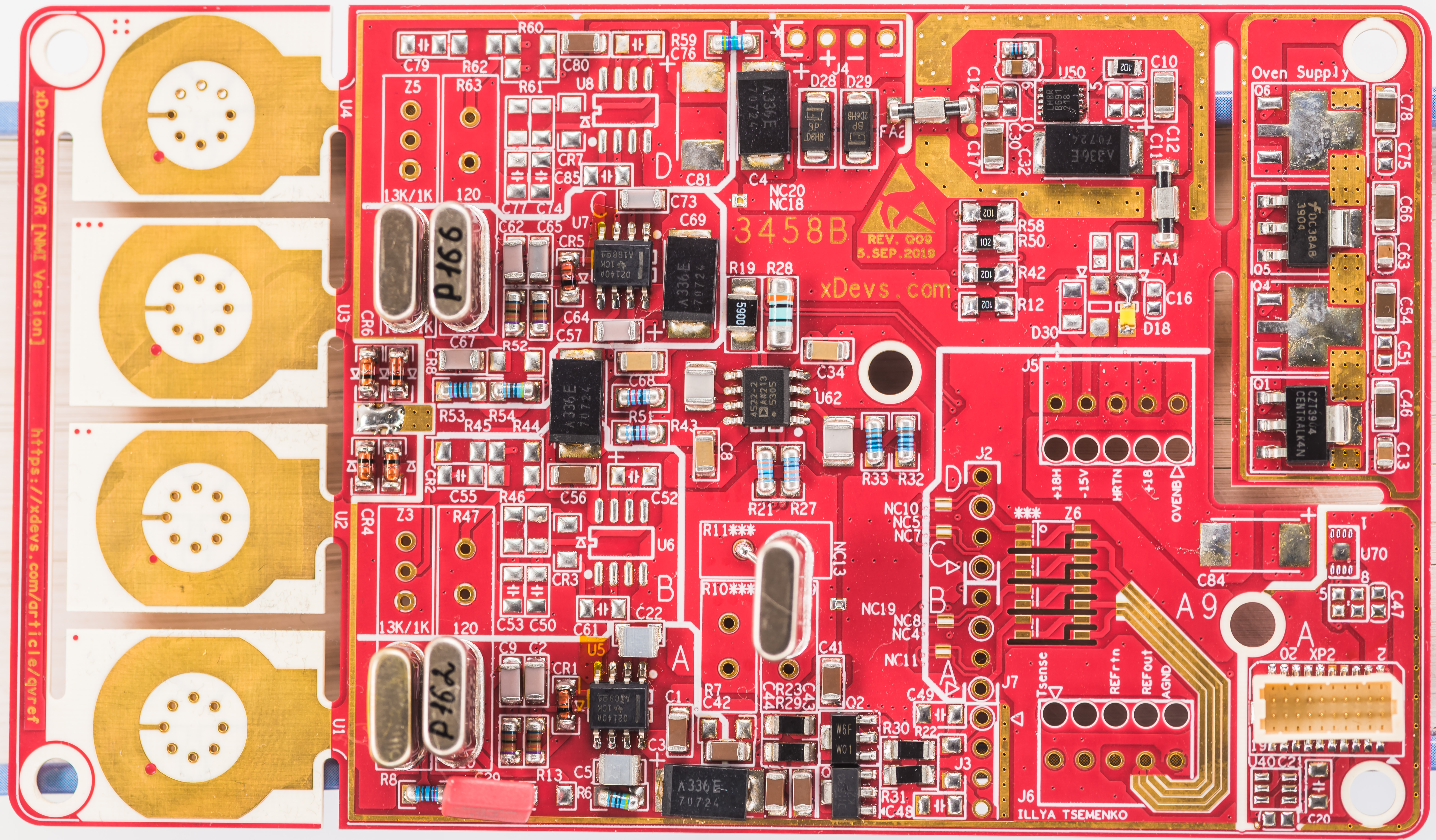
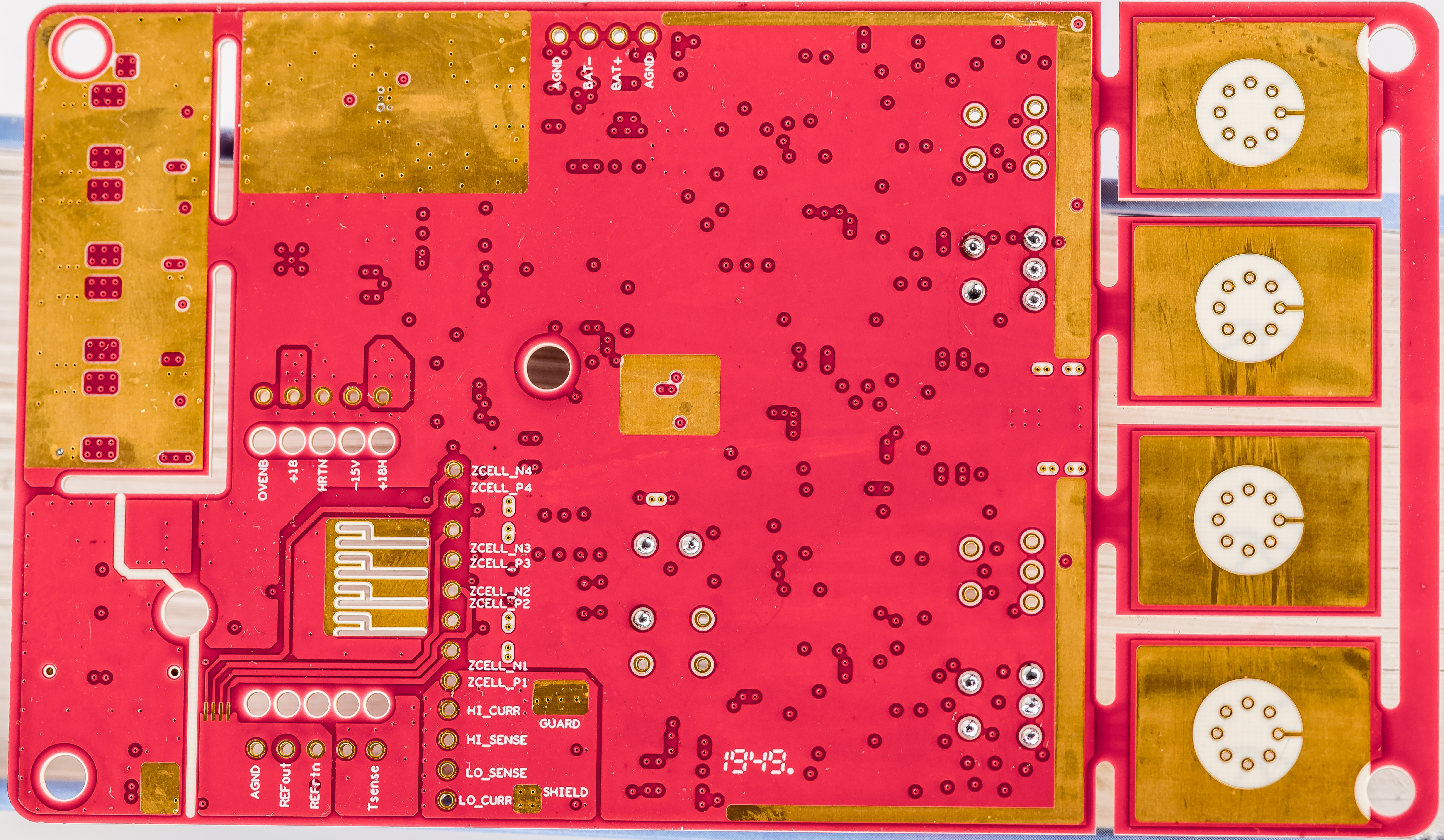
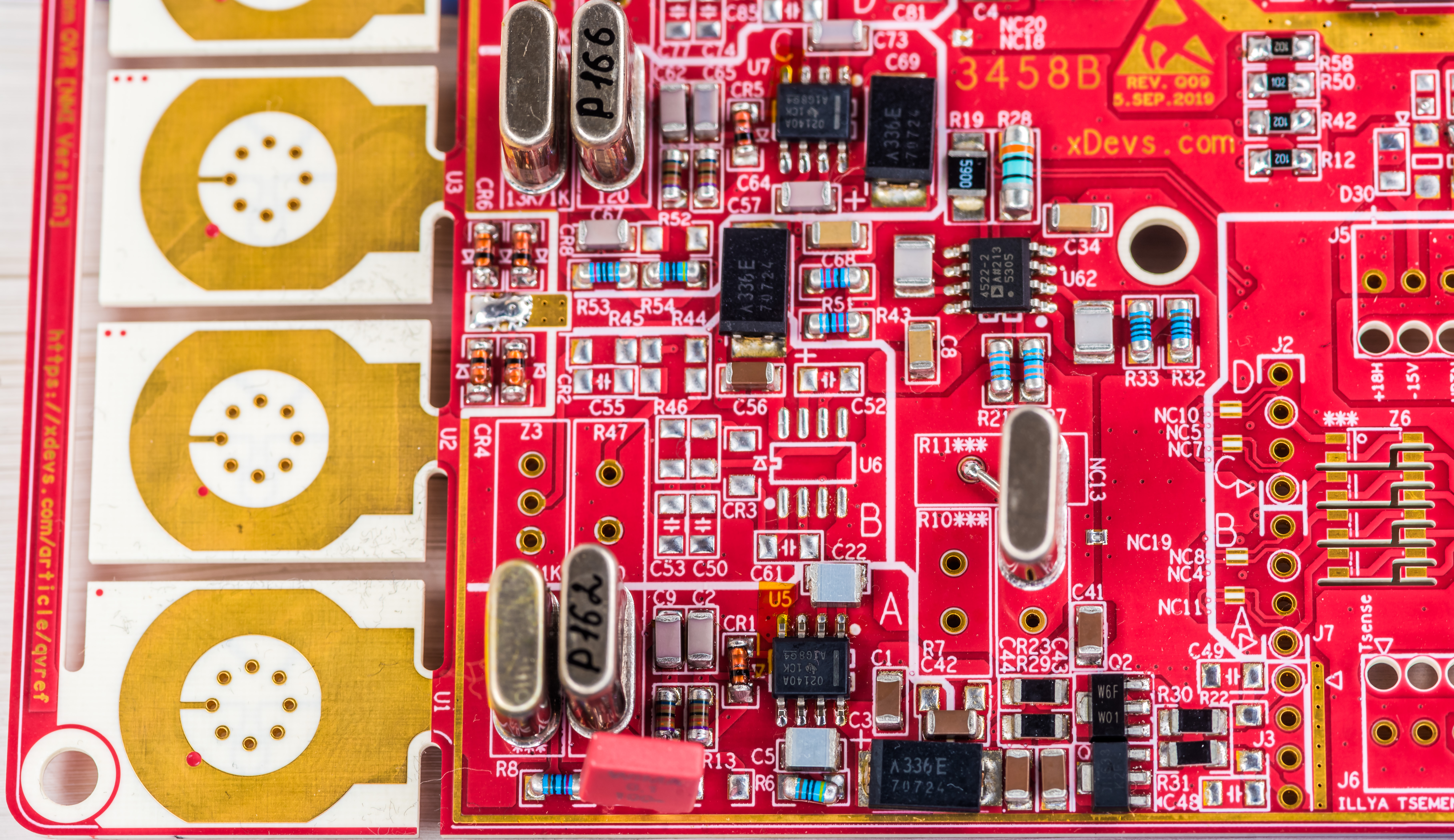
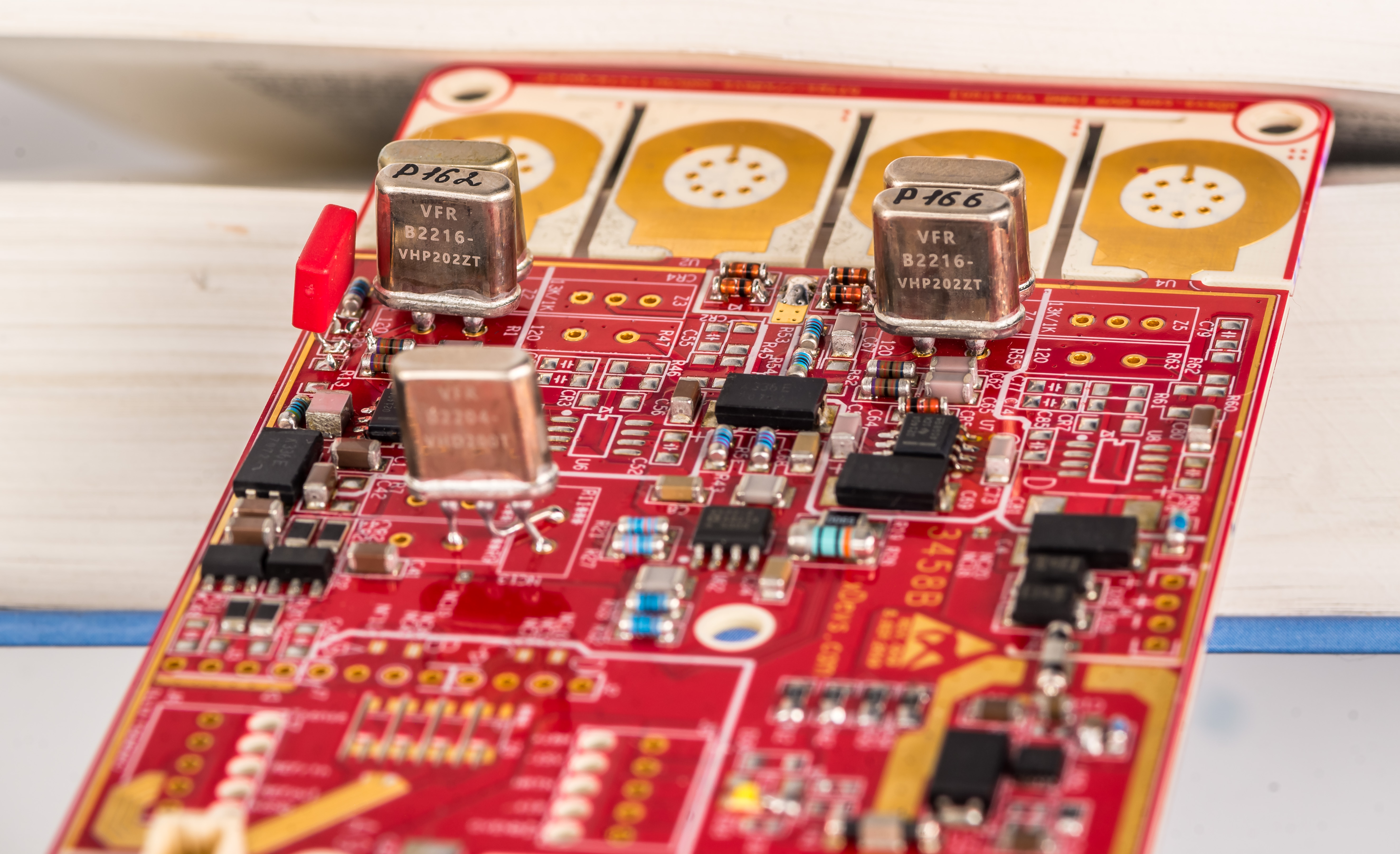
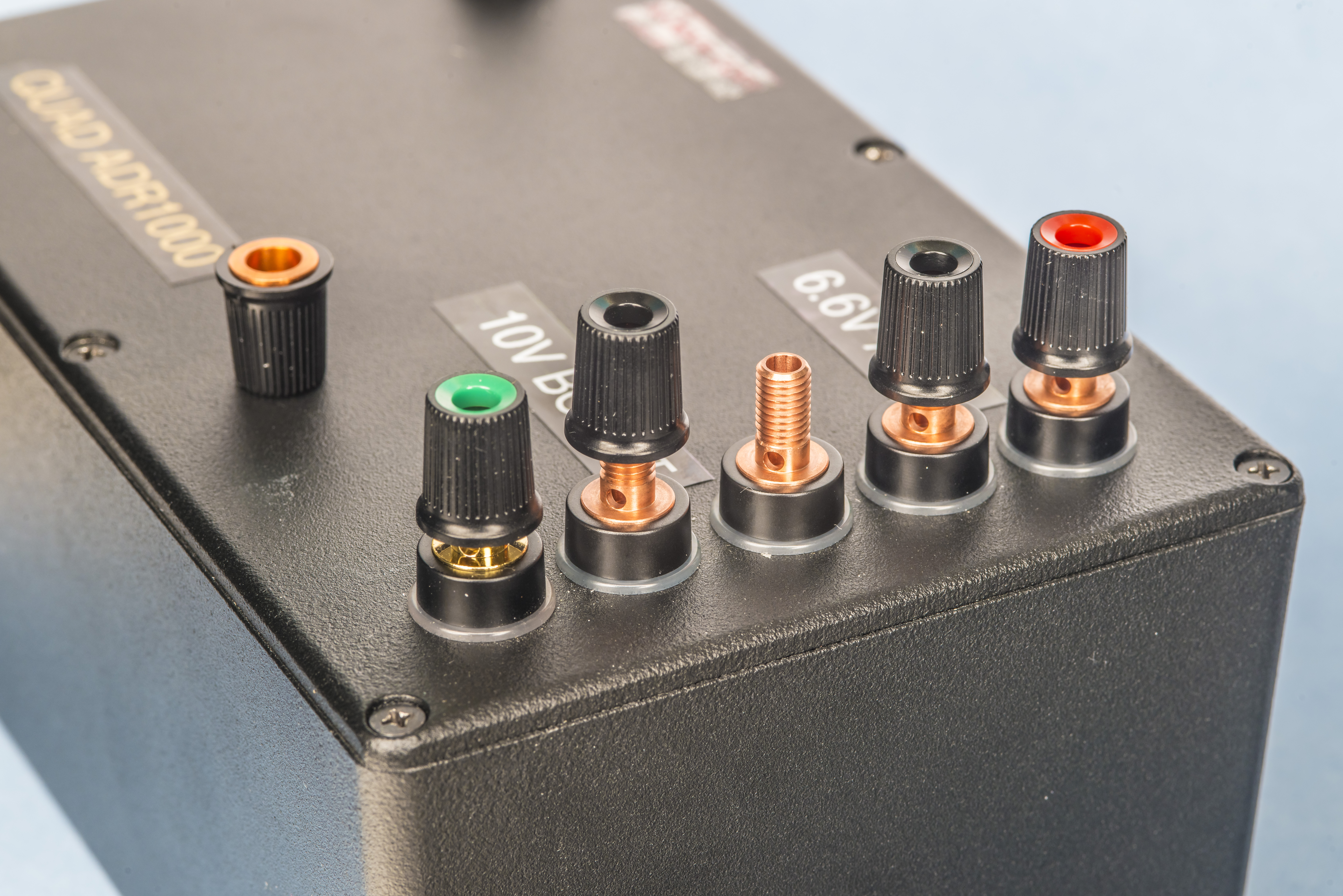
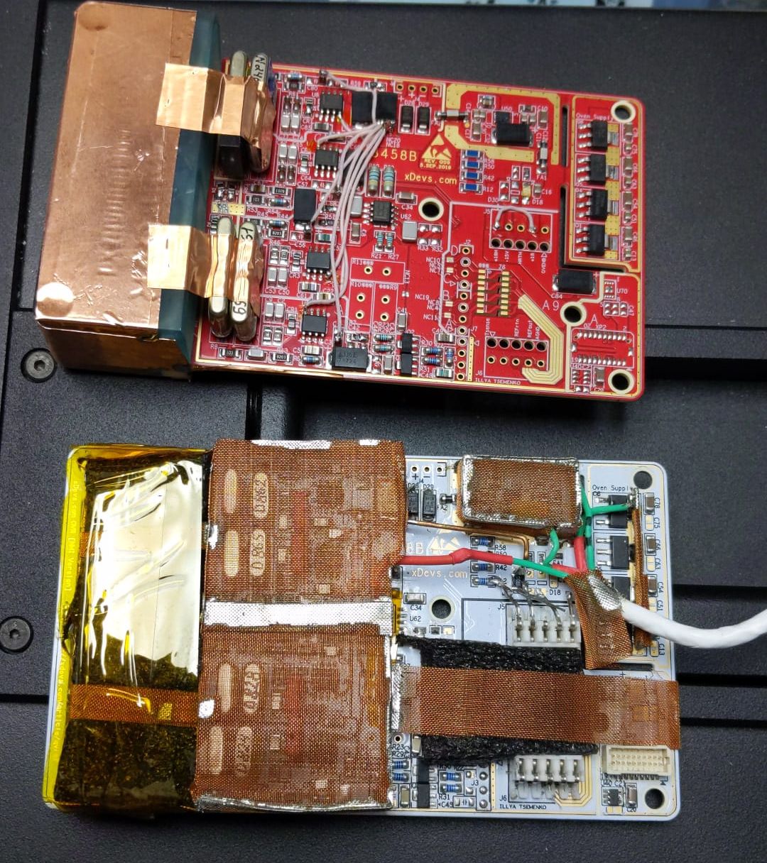
SN0005 – Quad Zener-chip comparison module with direct outputs
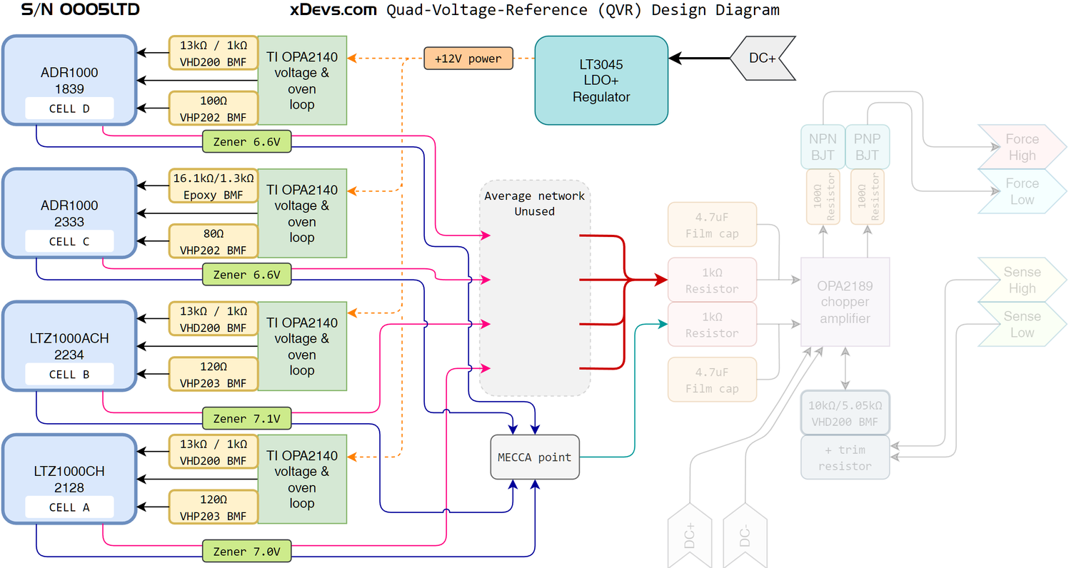
Purpose of this build is to run different chips in the same PCBA in same conditions and compare their long-term stability. No magical special aging was performed on any of the chips. They sat on the shelf unused for some time and now just soldered on the board fresh.
| Parameter | Cell A | Cell B | Cell C | Cell D |
|---|---|---|---|---|
| Zener type | LTZ1000CH | LTZ1000ACH | ADR1000AHZ | ADR1000AHZ |
| Date code | 28 week 2021 | 34 week 2022 | 33 week 2023 | 39 week 2018 |
| Temp setpoint | 13 kΩ / 1 kΩ VHD200 | 16.0674 kΩ / 1.3015 kΩ | 13 kΩ / 1 kΩ VHD200 | |
| Iz set resistor | 120 Ω VHP203T | 80 Ω VHP202T | 100 Ω VHP202T | |
| Temp point voltage | 0.506 V | 0.511 V | 0.495 V | 0.472 V |
| Iz voltage, measured | 0.4240 V | 0.429 V | 0.4846 V | 0.4734 V |
| Iz current, calculated | 3.53 mA | 3.57 mA | 6.06 mA | 4.73 mA |
| Opamp | TI OPA2140 | |||
| Q1 resistor | Susumu 68 kΩ | MELF 62 kΩ | ||
| Q2 resistor | Susumu 68 kΩ | MELF 62 kΩ | ||
| FB capacitors | 0.15 uF 1206 film | |||
| TC trim | 150 kΩ | 820 kΩ | 332 kΩ | 820 kΩ |
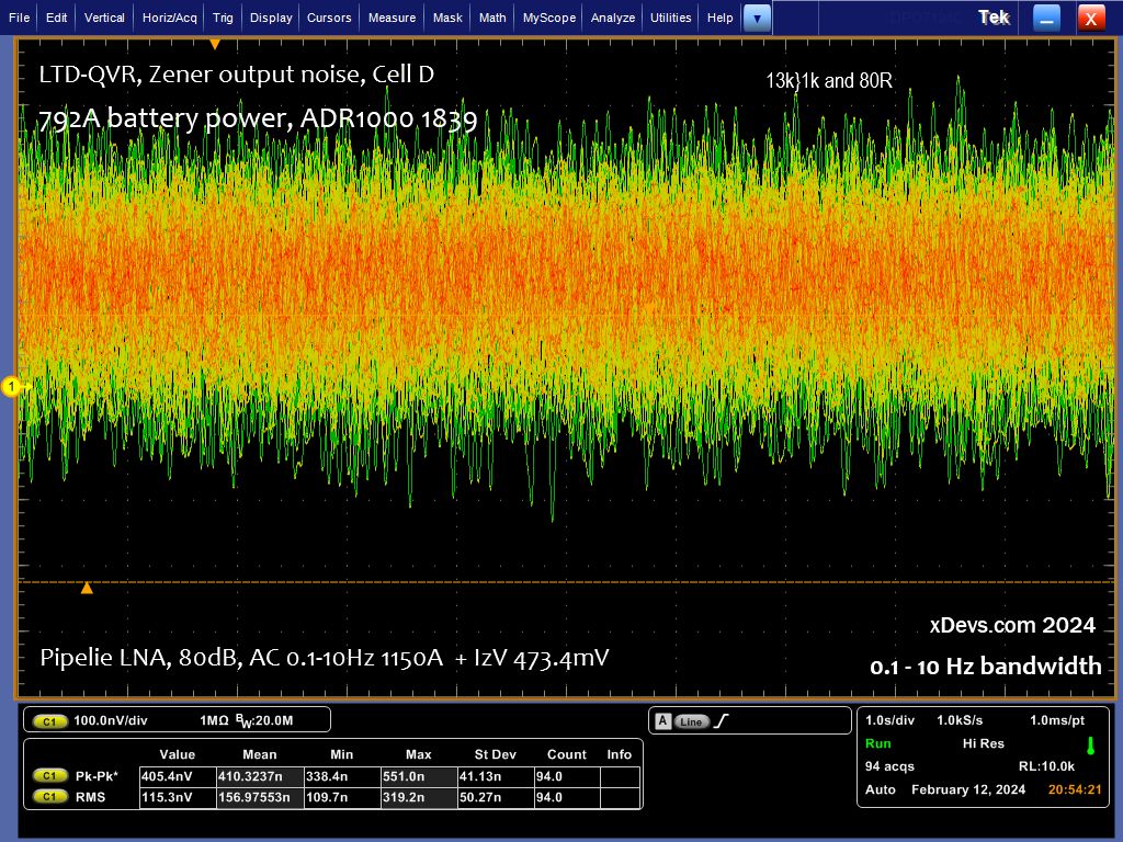
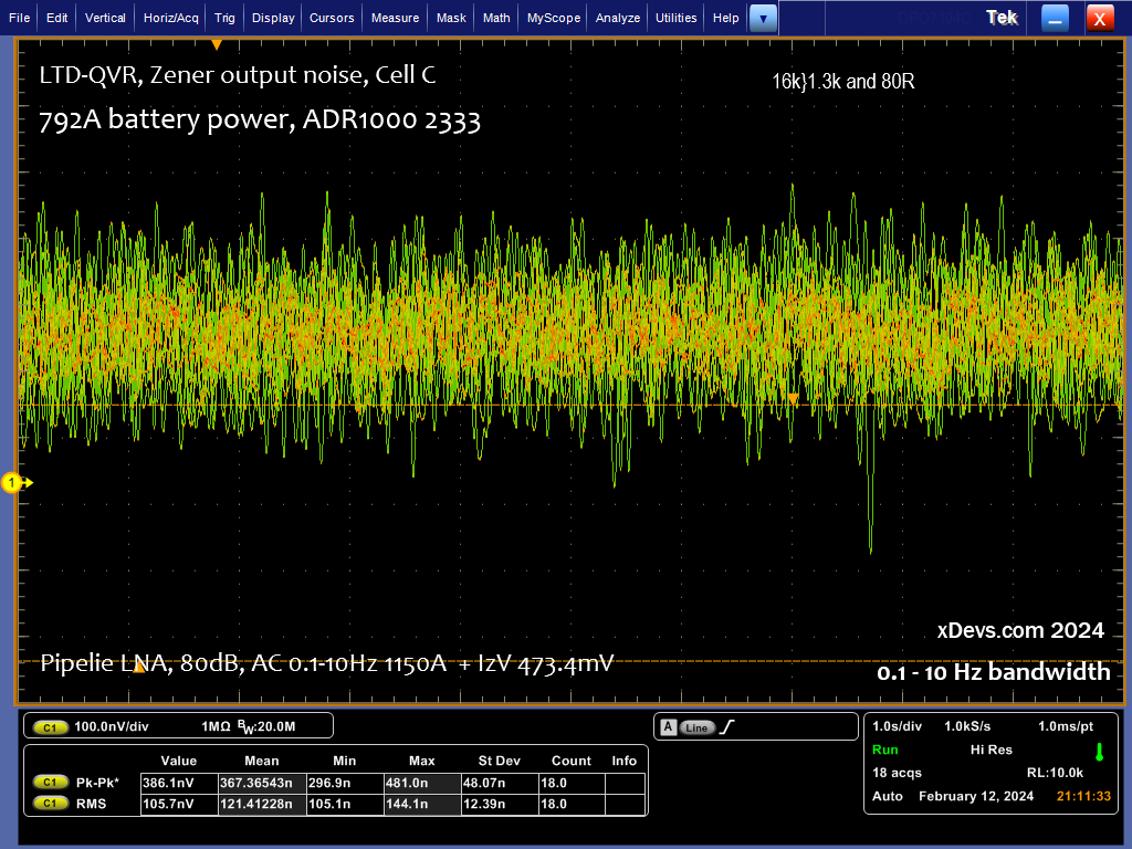
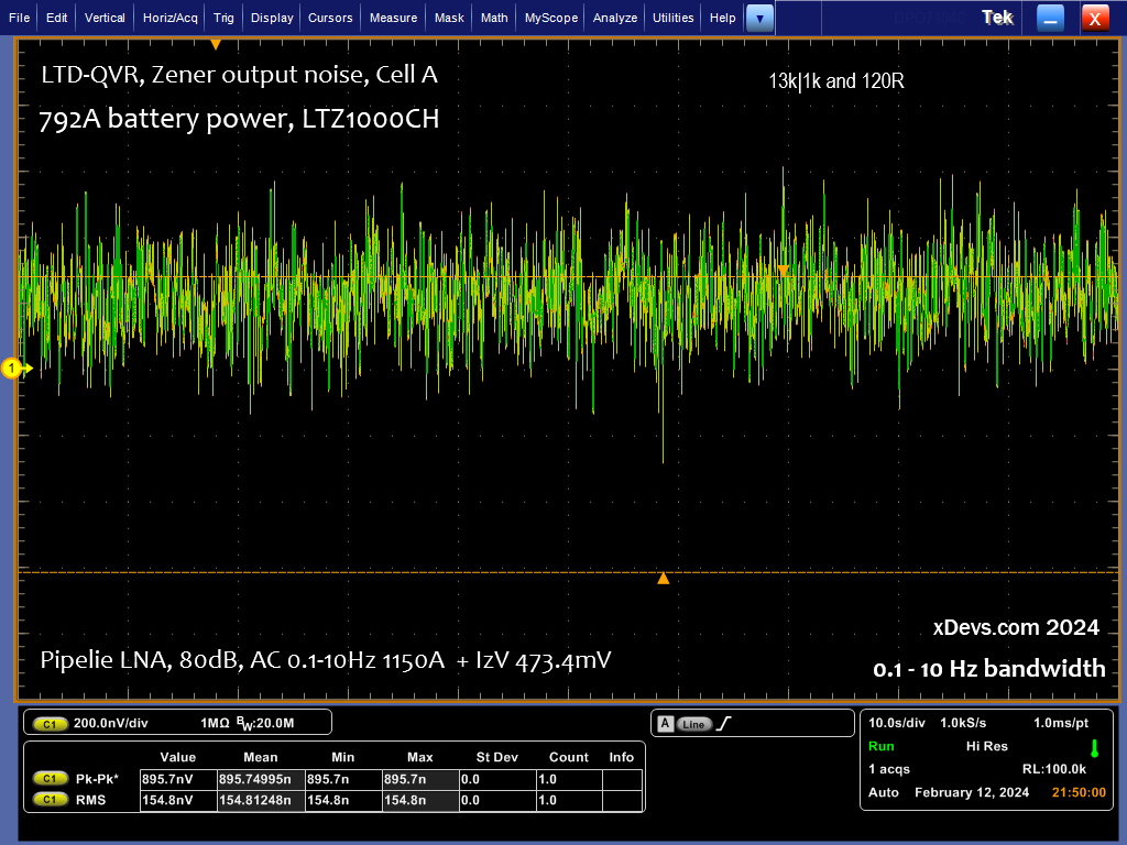
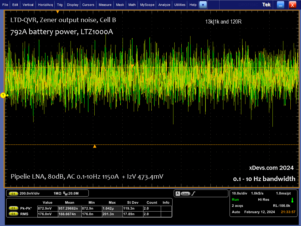
| Noise, 0.1 Hz – 10 Hz | 895 nV pk-pk | 957 nV pk-pk | 367 nV pk-pk | 410 nV pk-pk |
| Initial voltage, FEB.13.2024 | 7.17232133 V | 7.09003609 V | 6.60987871 V | 6.62218042 V |
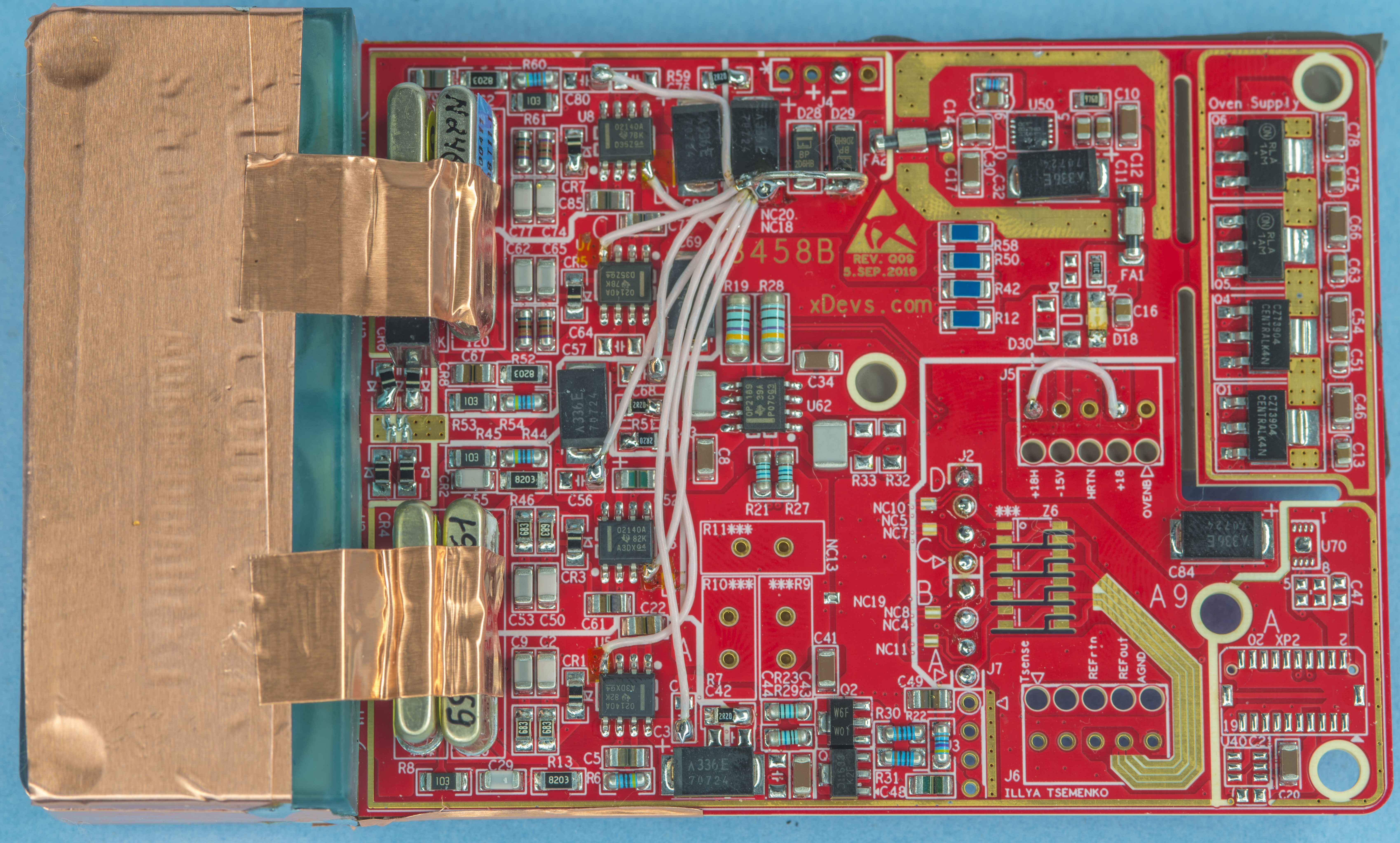
Board as assembled. Standard Sn60Pb40 solder paste was used to mount all the passive and active components.
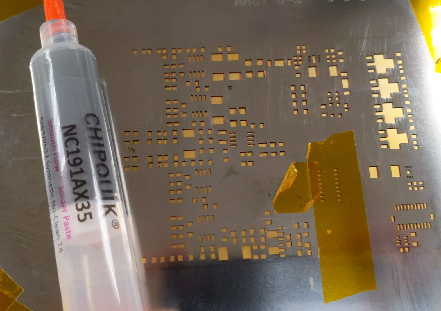
All SMT parts were soldered in convection 6-zone oven using maximum temperature +215 °C.
Zener chips and resistors soldered by hand using Sn60Pb40 solder.
Onboard power supply configured to provide +12.0 V, using LT3045-1EDD regulator with 4.7 µF 0805 feedback capacitor. Output stage is configured with OPA2189 and discrete output NPN+PNP stage but currently unused. Averaging of zener outputs is also unused (Z6 network is not populated).
All chips are populated at about 2-3 mm gap from the PCB surface.
QVR PCB has few layout issues, so this board mitigated that with a rework. Zener opamps ground is incorrectly routed to signal return plane instead of power supply “noisy” ground. This also affect decoupling capacitor. So running separate ground required tomb-stoning capacitors and isolating pin 4 on the each OPA2140 opamp from PCB by small kapton tape pad. Then all floated connections routed to power ground at the capacitor C4 per star wiring.
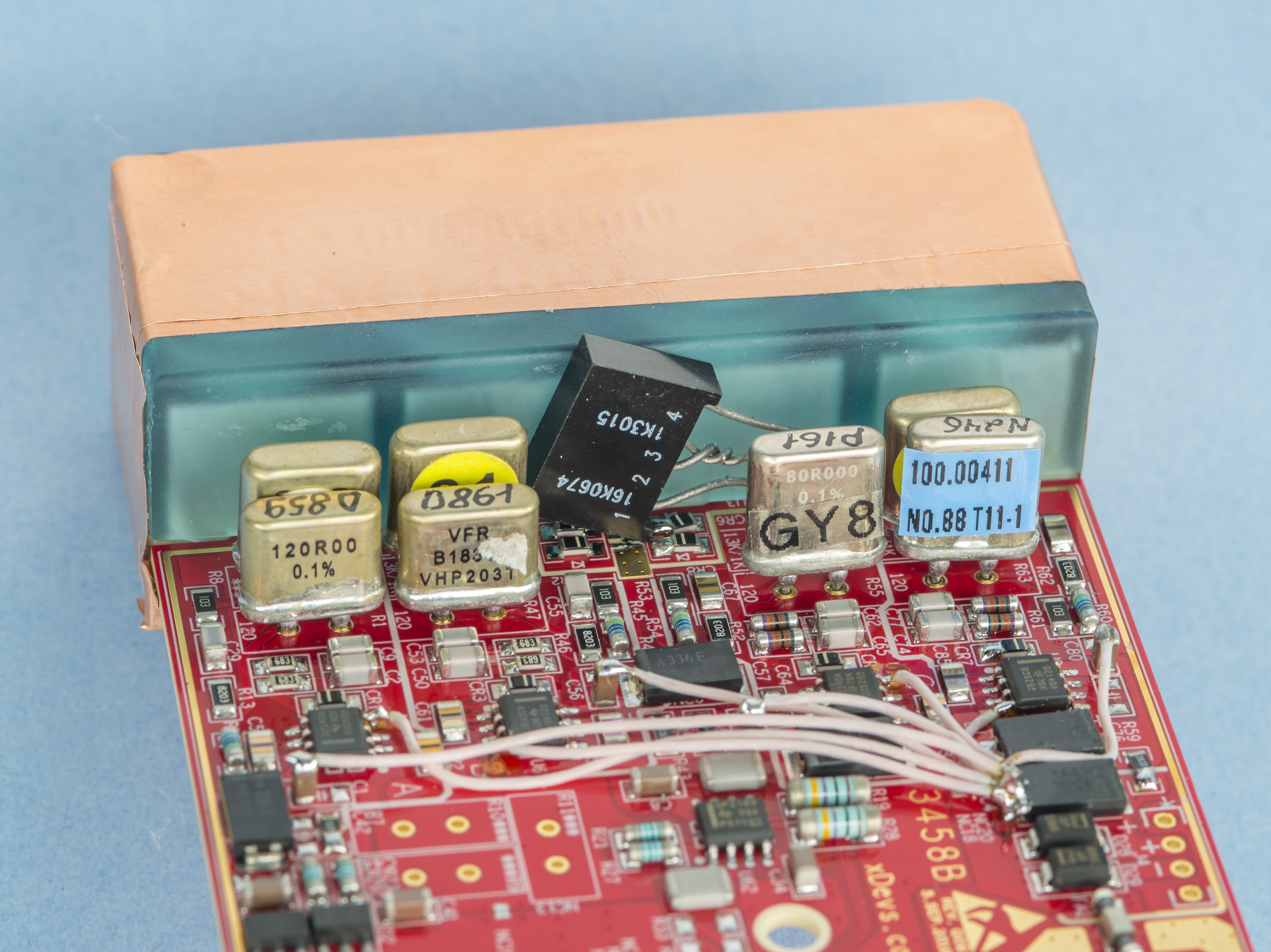
Cell C used epoxy BMF resistor network based on S102 elements for temperature setpoint. Rest of resistors are hermetic metal foils.
Both sections of the PCB zones with zener chips isolated from airflow by 3D-printed plastic cap from both top and bottom side.
Caps are covered together with 0.25 mm thick copper adhesive tape. Each piece of tape was connected electrically together and tied to ground potential at the PCB in one point.
Back of the PCB area under OPA2140 opamps and foil resistors was also taped with solid copper tape placed on top of 2 layers of kapton tape for insulation.
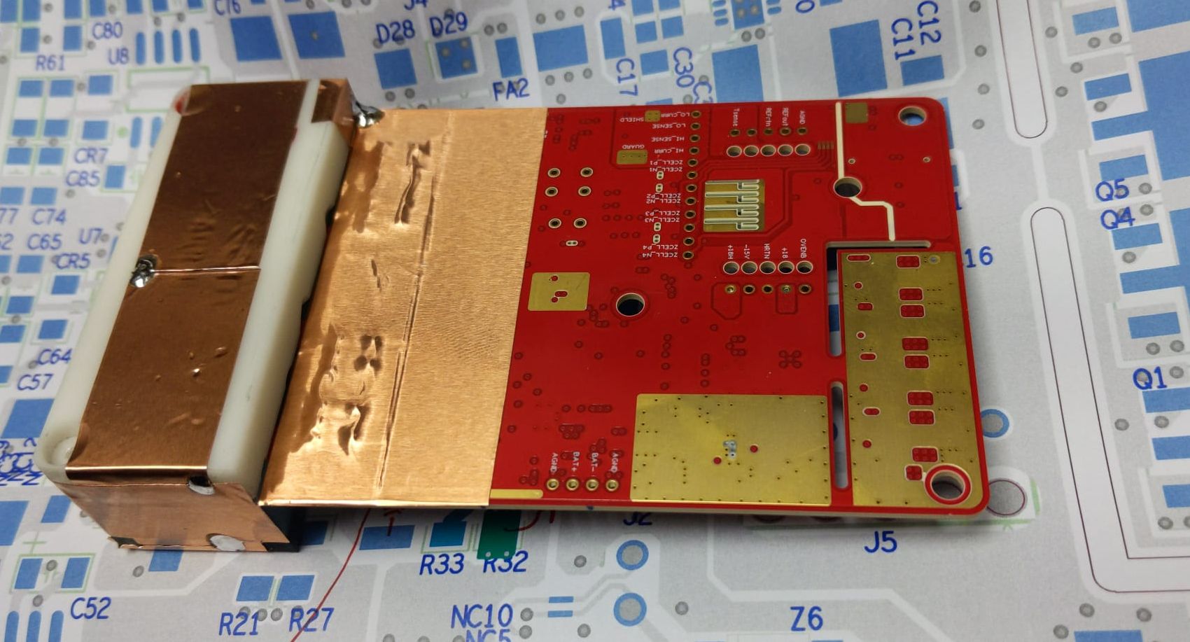
Individual zener voltages are available on J2 and J7 pin header ports in the bottom right side of PCBA.
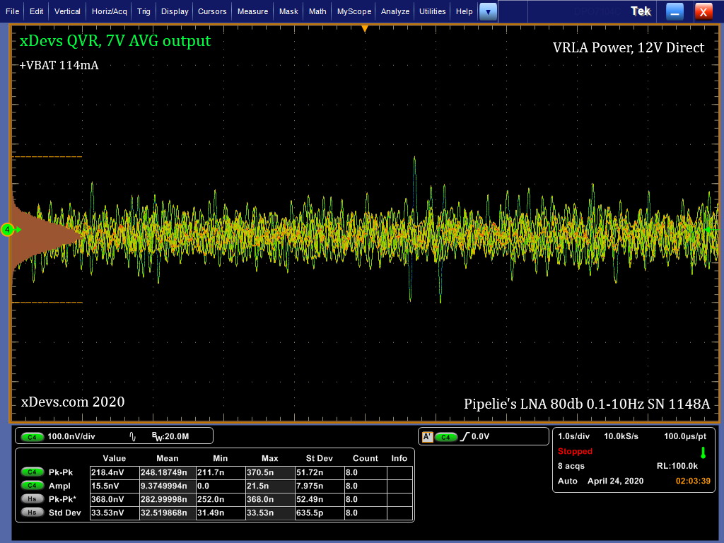
Noise measurements with 80 dB amplifier with Cell C and Cell D:
Noise measurements with 80 dB amplifier with Cell A and Cell B. Please note larger 200 nV/division vertical scale on the plots.
Visual comparison to the very old SN0002 quad-LTZ1000ACH module, used to test noise limits of 3458A:
And here we will keep track on long-term drift data points. Board was first powered up February 13, 2024 at 1:46 am.
| Parameter | Cell A | Cell B | Cell C | Cell D | Test duration |
|---|---|---|---|---|---|
| Zener type, datecode | LTZ1000CH, 2128 | LTZ1000ACH, 2234 | ADR1000AHZ, 2333 | ADR1000AHZ, 1839 | |
| Module power applied, TC trim initial | 820 kΩ | 820 kΩ | 820 kΩ | 820 kΩ | |
| Output voltage, FEB.13.2024 | 7.17232149 V | 7.09003469 V | 6.609880 V | 6.62218042 V -> 6.622153 V | 55612 seconds |
| Module power applied, TC trim 1 | 240 kΩ | 820 kΩ | 680 kΩ | 820 kΩ | |
| Output voltage, FEB.14.2024 | 7.17232247 V | 7.08996560 V | 6.609873 V -> 6.609882 V | 6.622153 V -> 6.622119 V | 143487 seconds |
| Module power applied, TC trim 2 | 150 kΩ | 820 kΩ | 332 kΩ | 820 kΩ | |
| Output voltage, FEB.15.2024 | 7.17231999 V | 7.08990526 V | 6.60982031 V | 6.62211983 V | 187163 seconds |
| Module power applied, TC trim 3 | 150 kΩ | 820 kΩ | 500 kΩ | 820 kΩ | |
| Output voltage, FEB.17.2024 | 7.17232449 V | 7.08991079 V | 6.60989303 V | 6.62208501 V | 111618 seconds |
Temperature coefficient results after trim 2 show great results, except Cell C. Went too aggressive with 332 kΩ resistor there, need more in range 450-500 kΩ instead.
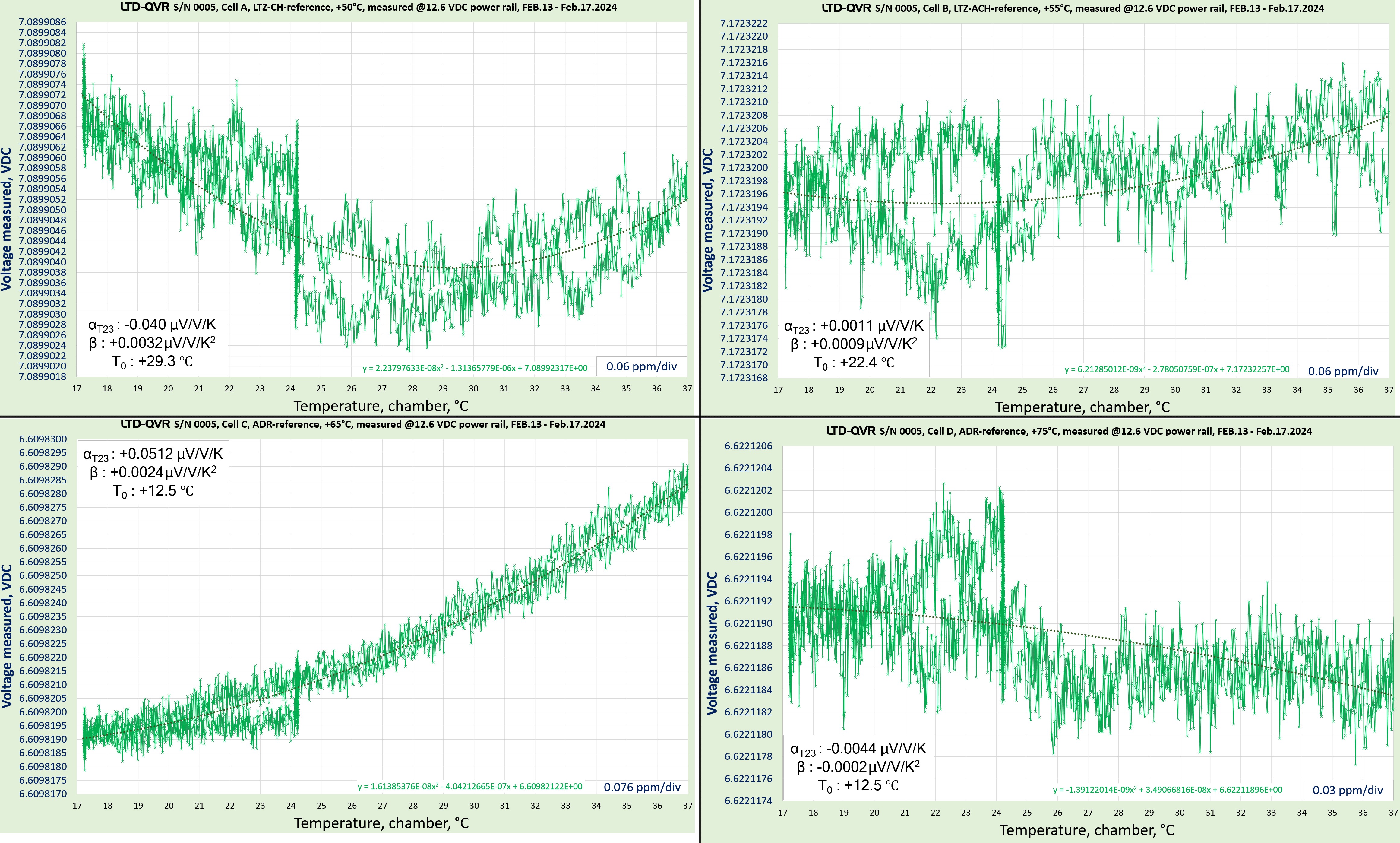
And final retrim:
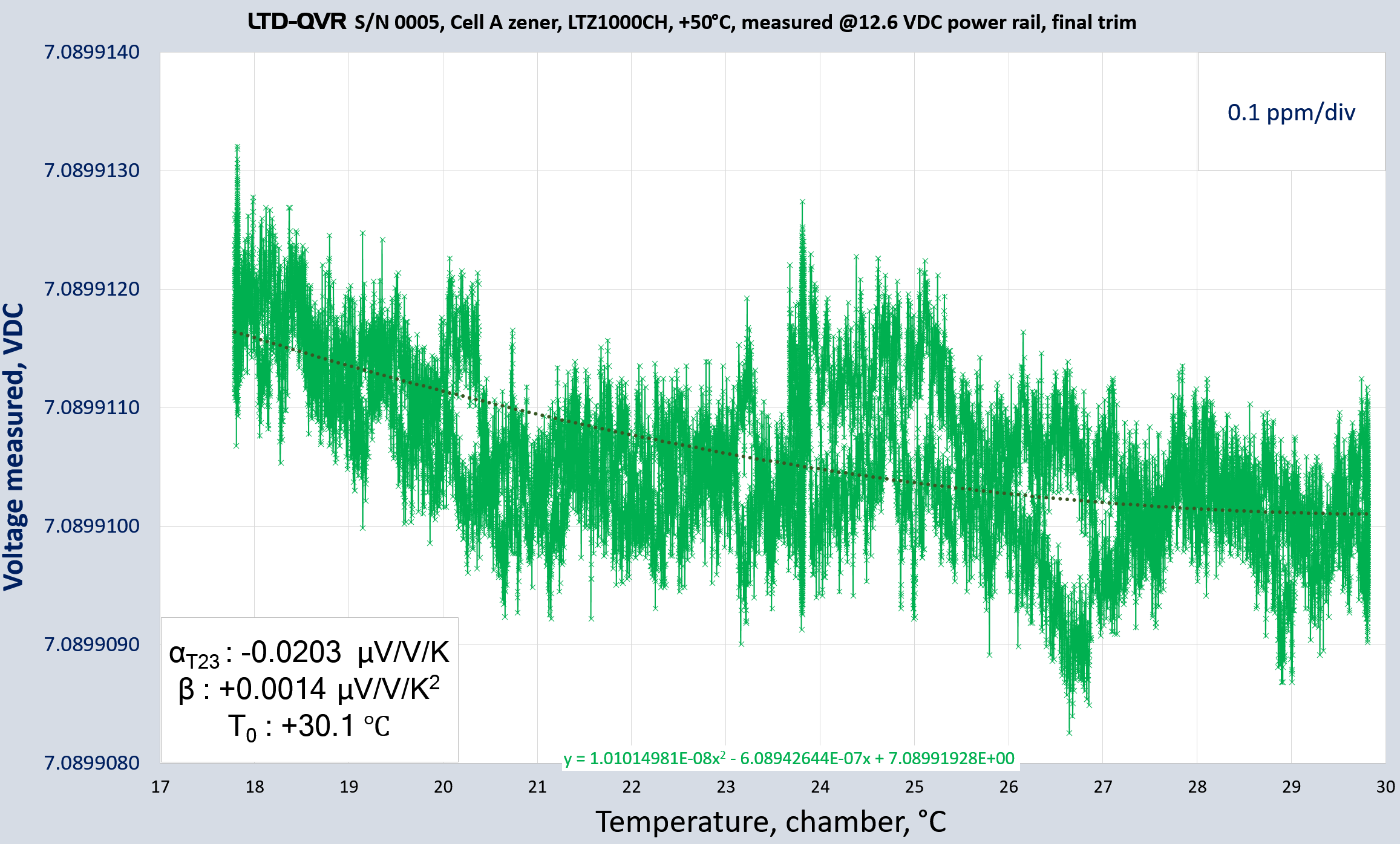
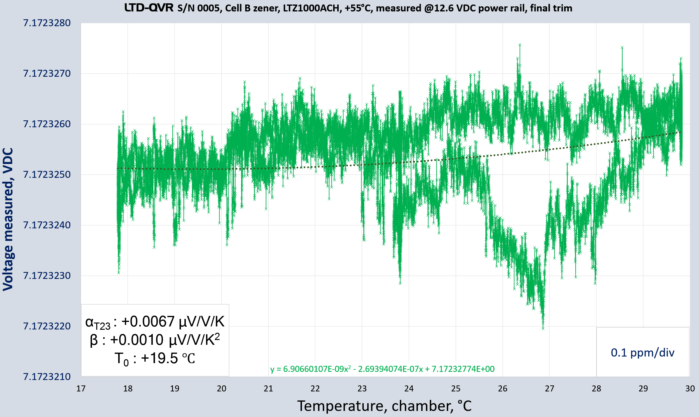
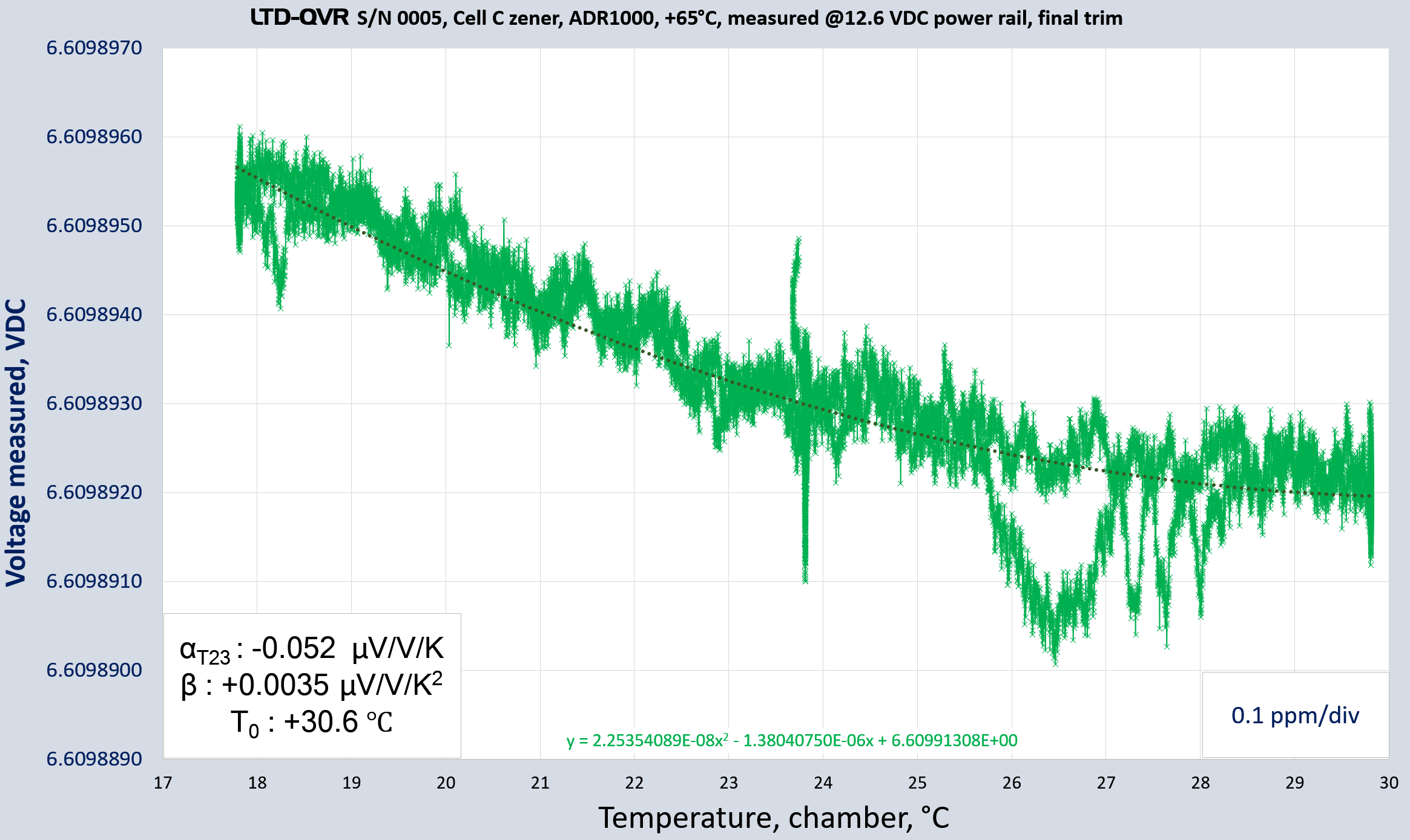
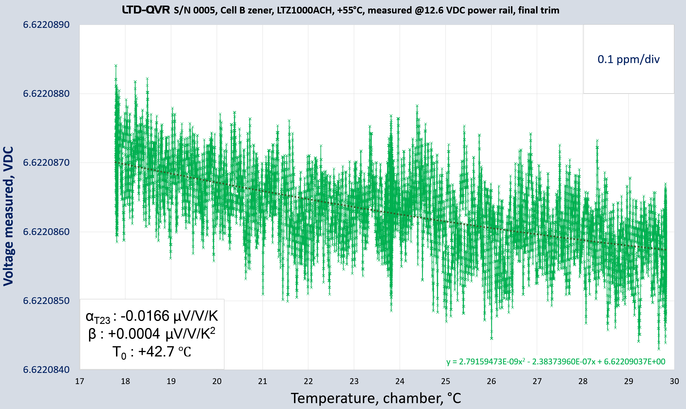
Cell C is still little bit higher tempco, but it was determined to leave it as is. Total time that reference module spent powered up during thermal cycles and initial check runs is 505524 seconds ±600 seconds, or 140.4 hours.
SN0005 Long-term drift comparison
After tempco trimming and adjustments on module SN0005 completed this module was permanently connected to zener array bank per NIST TN430 with series-opposition connected scanned zeners and nanovoltmeter. This will allow us to collect long-term drift data with one sample/zener collected every 1.5 hours.
March 2024 data : 700 hours
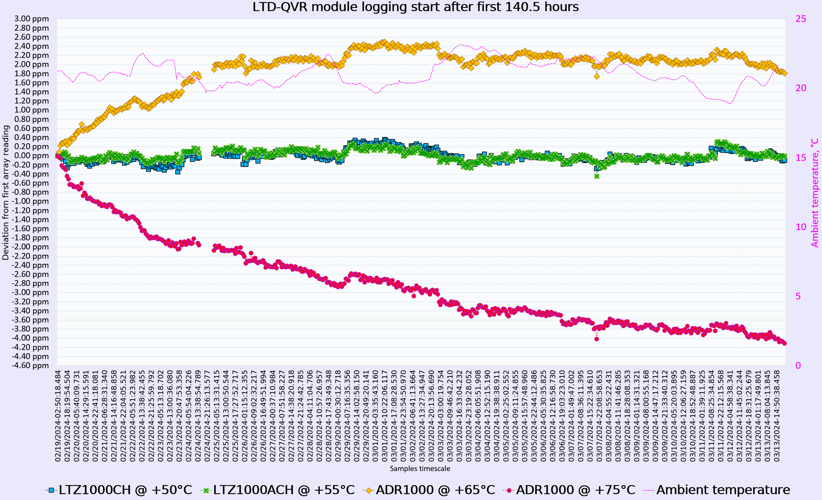
After running reference powered up for total 700 hours (first 140.5 hours are omitted from plot, “zero” reference taken on 19 February, 2024) drift difference between different chips is quite noticeable.
Both LTZ1000CH and LTZ1000ACH demonstrate clear absence of any significant drift, which underline excellent performance of LTZ design once again. All we can see on LTZ outputs is just residual temperature coefficient play and random noise walk up and down. Worst outlier points for these chips staying within ±0.4 µV/V from initial point on 19 February, 2024.
ADR1000 chips however are not so stable and have significant drift. Newer 33 week 2023 chip which is running at +65 °C oven setpoint demonstrated upward +2.0 µV/V drift in first 8 days from zero point and then somewhat stabilized with walk around ±0.3 µV/V. Older 2018 week 39 chip running at hotter +75 °C (as datasheet recommends to us) and demonstrate opposite drift of -4.2 µV/V and still going. There is no visible stabilization time for this chip, just like with other 1839 chips from older module we explored in long-term drift study page.
Based on this time frame conclusion is:
1. LTZ1000-based solutions already able to stabilize in time period less than 140 hours after assembly.
2. New year 2023 week 33 ADR1000 chip shows promising stabilization time, more into future will determine if this statement holds.
3. Old year 2018 week 39 ADR1000 chip does not stabilize in 700 hours timeframe after assembly.
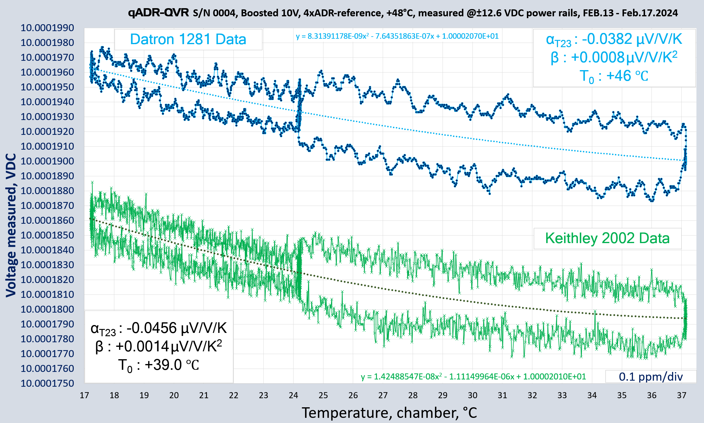
May 2024 data : 2544 hours
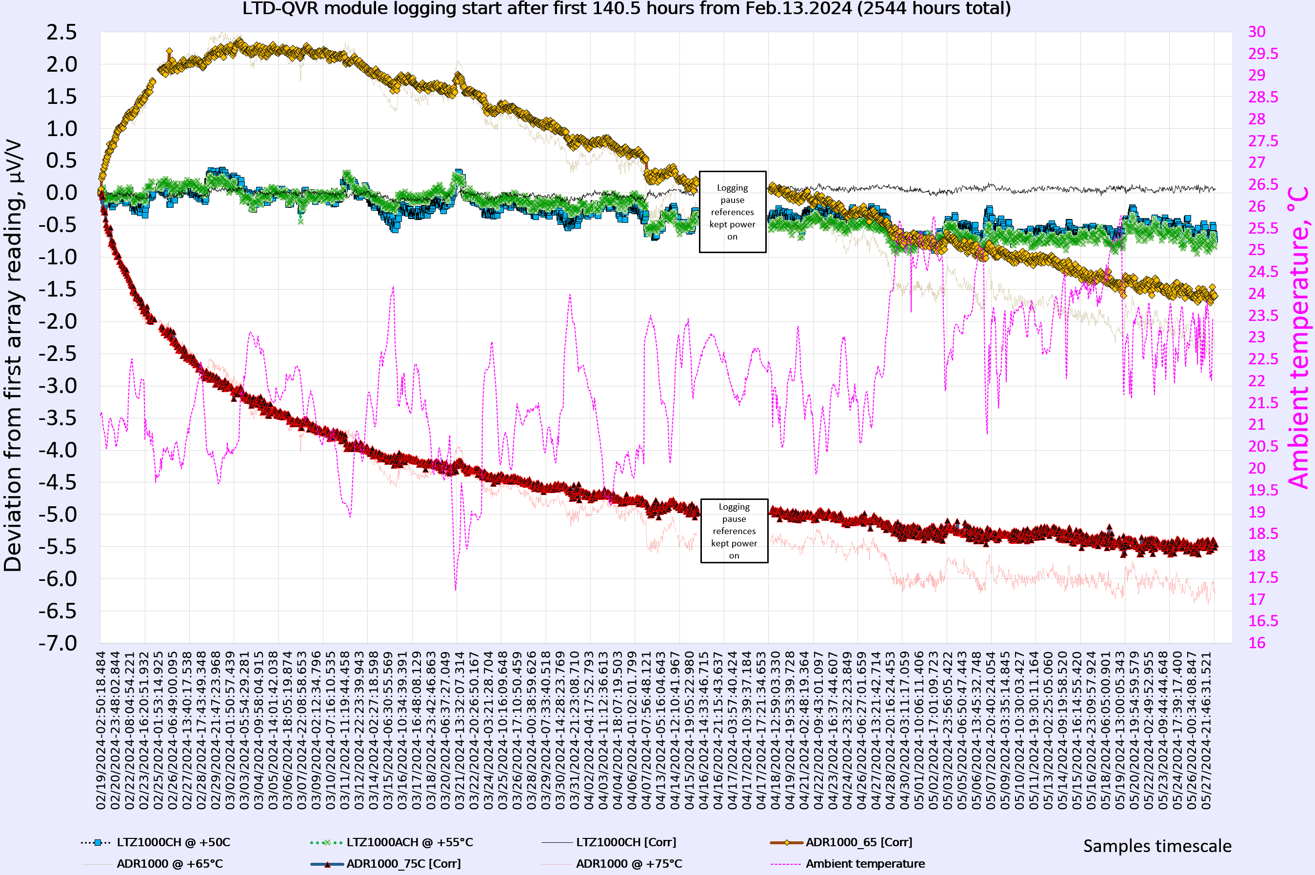
Updated dataset with 2544 hours of runtime on QVR comparison module shows us some new information. Finally difference of performance from the ADR1000 chip running at +65 °C and one at hotter +75 °C becomes visible. Both LTZ1000 and LTZ1000A still continue to offer far superior stability to the new redesigned reference, with worst deviation at -0.9 µV/V after equal runtime duration, compared to -5.5 µV/V that hotter ADR1000 shows.
Voltage bank array was scanning some another experiment from April 16 till April 18 which is reflected as a gap in data on the chart. References were kept untouched and still powered in this data collection gap.
Based on this time frame data conclusion is:
1. LTZ1000-based solutions demonstrate excellent stability with predictable linear drift downwards.
2. ADR1000 chip at +65 °C reversed it’s drift direction and now continue to drift downwards at fairly large slope.
3. ADR1000 chip at +75 °C always had drift down and now settling to more linear trend faster than colder oven chip.
4. Statement 2 from the previous 700 hour dataset now not confirmed to be true.
June 2024 data : 3120 hours
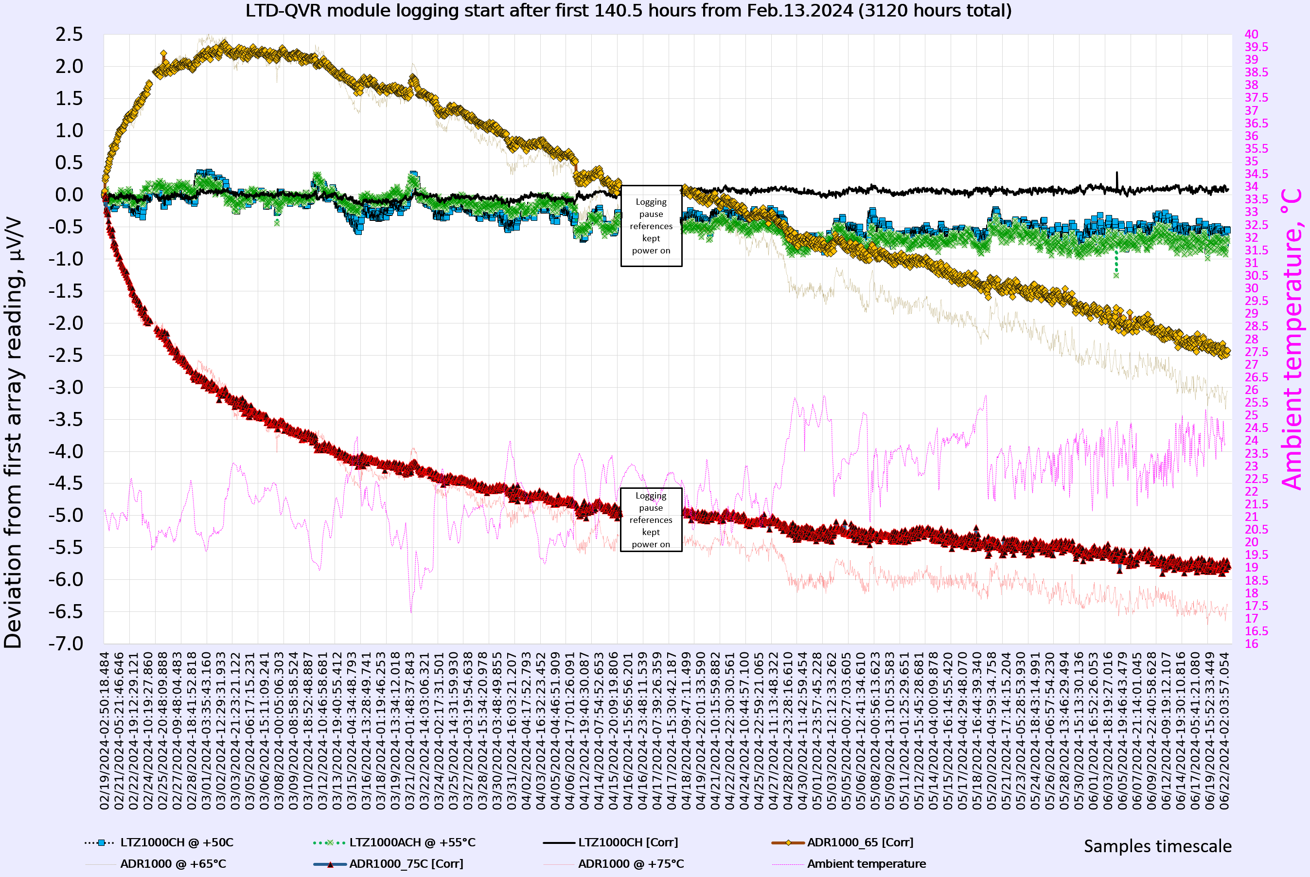
To stir things up a little bit the board was powered off on June 22, 2024 3:00pm and baked in the convection oven at around +115 °C for 8 hours. Reference module was unpowered during whole baking duration.
Complete data log for QVRL SN0005 module
| Parameter | Cell A | Cell B | Cell C | Cell D | Test duration |
|---|---|---|---|---|---|
| Zener type, datecode | LTZ1000CH, 2128 | LTZ1000ACH, 2234 | ADR1000AHZ, 2333 | ADR1000AHZ, 1839 | |
| Module power applied, TC trim 3 | 150 kΩ | 820 kΩ | 500 kΩ | 820 kΩ | |
| Output voltage, FEB.17.2024 | 7.17232449 V | 7.08991079 V | 6.60989303 V | 6.62208501 V | 111618 seconds |
| Output voltage, FEB.19.2024 by XBank | 7.17230188 V | 7.08989138 V | 6.60987132 V | 6.62205624 V | |
| Output voltage, MAR.14.2024 by XBank | 7.17230242 V | 7.08989216 V | 6.60988050 V | 6.62203468 V | |
| Output voltage, MAY.28.2024 by XBank | 7.17229696 V | 7.08988762 V | 6.60985202 V | 6.62202025 V |
SN0020 – Updated revision 2 QVR module with ADR1000
QVR design was revised and updated in May 2024 to account for ADR1000-tailored tweaks. These changes and design details were discussed and reviewed in internal tracker #512. Some of the main changes are as following:
- Fix : Ground at the cell amplifiers is returned to power ground, instead of signal ground to reduce noise injection to voltage signal path.
- Fix : Ground at the cell tantalum caps to return into power ground instead of signal ground to reduce noise injection to voltage signal path.
- Fix : Top connector for HP meter A9 interface footprint is fixed now (original J5 was incorrectly mirrored)
- Fix : Output scaling has incorrect feedback for negative side op-amp which caused excessive noise
- Change : Add wide SOIC16 footprint for more options in averaging resistor networks
- Change : Copper distribution tweaks
- Change : Replace analog MAX6610 temperature sensor with digital TMP119 and TMP117 (galvanic isolated ground/power from anything analog)
- Change : Rev2 board targeted for normal room temperature use only, as result Rogers dielectric replaced to cheaper S1000-2M TG170.
- Update : Added footprint option for VHD200 for scaling 6.6/7.2V => 10V network
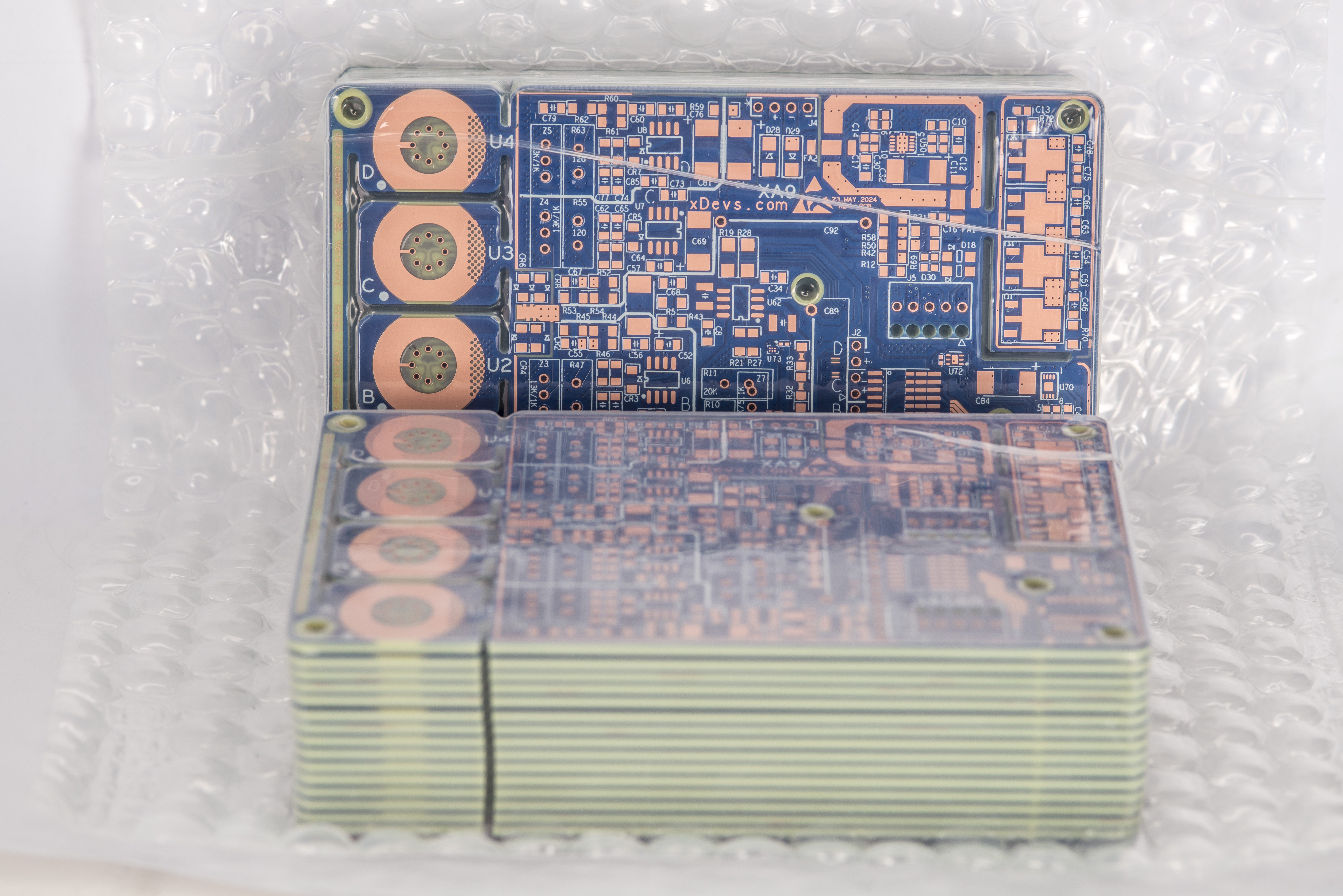
First batch of the boards and new solder-paste stencil was received June 6, 2024. General design, component choice and physical dimensions are nearly identical.
This QVR Rev2 board still require mechanical modifications on HP3458 A1 DC board to be used as low-noise 7V source, it is NOT plug-and-play ready.
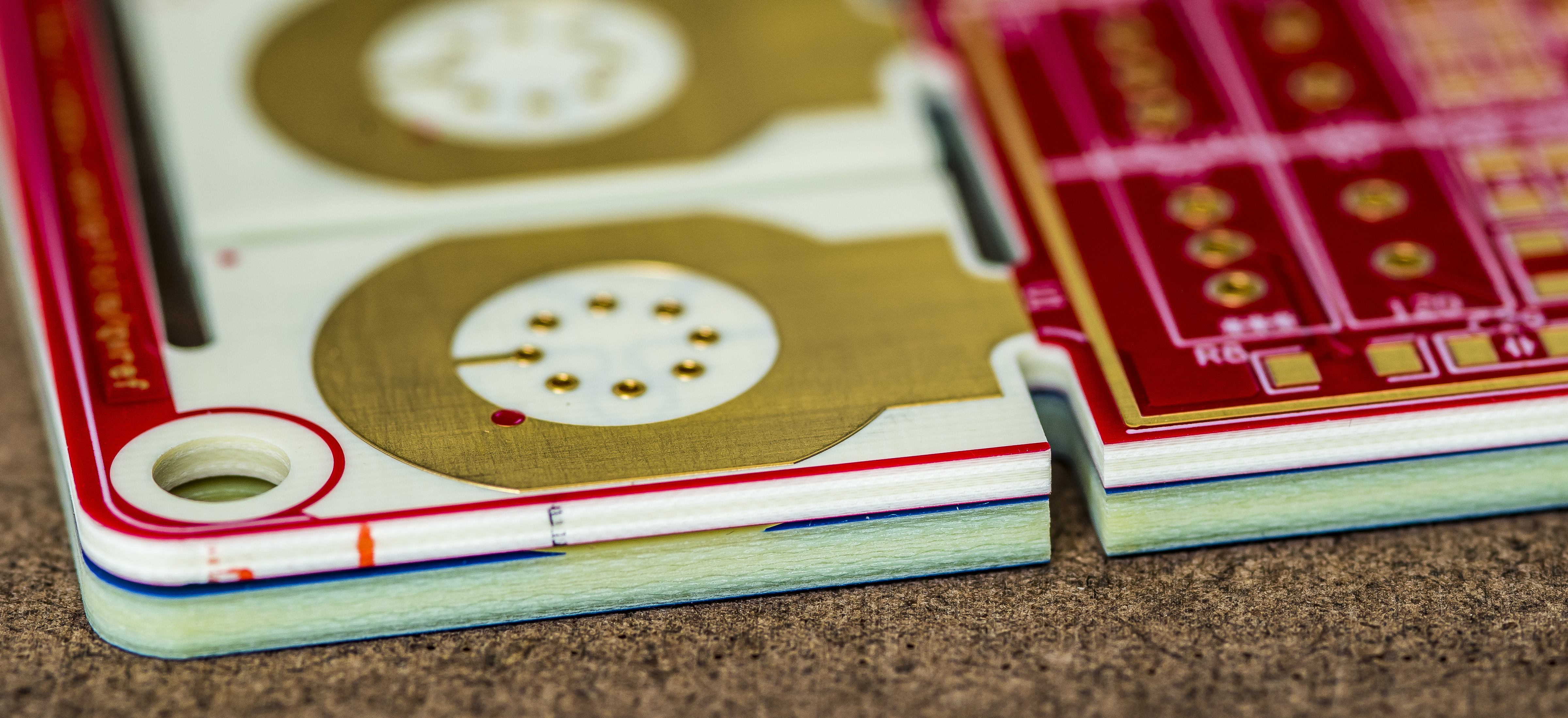
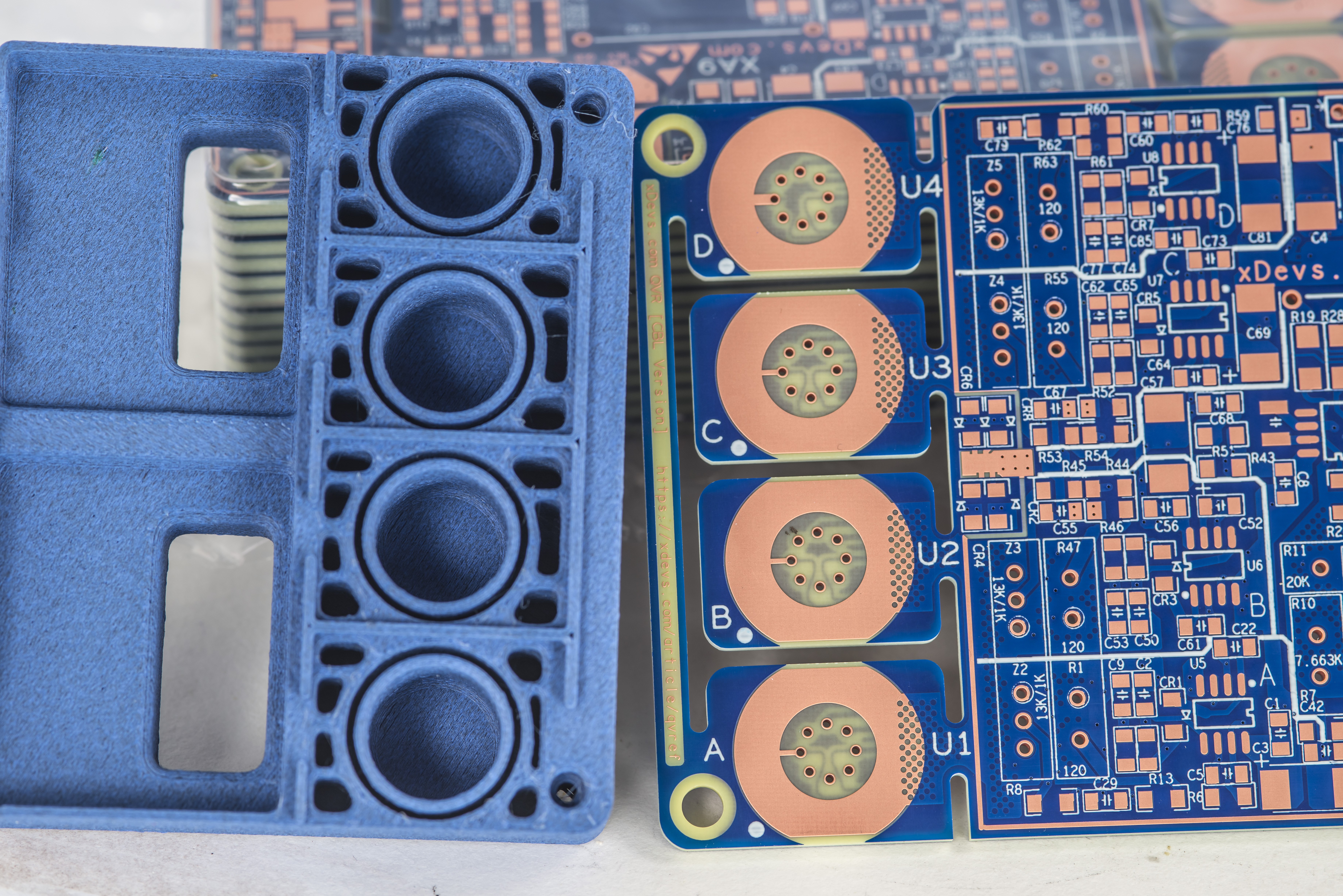
Updated boards went away from Au-over-Ni ENIG plating and now have exposed bare-copper pads with thin organic surface protection layer. This way every single nanovolt/°C will stay on the board :). There is a new Texas Instruments TMP119 U73 micro-BGA temperature sensor which is now placed near the center of the board. Tiny package can be also used a soldering challenge test. I’ve used this thermometer IC in the flexible temperature sensor design few months ago and really happy with the performance and accuracy.
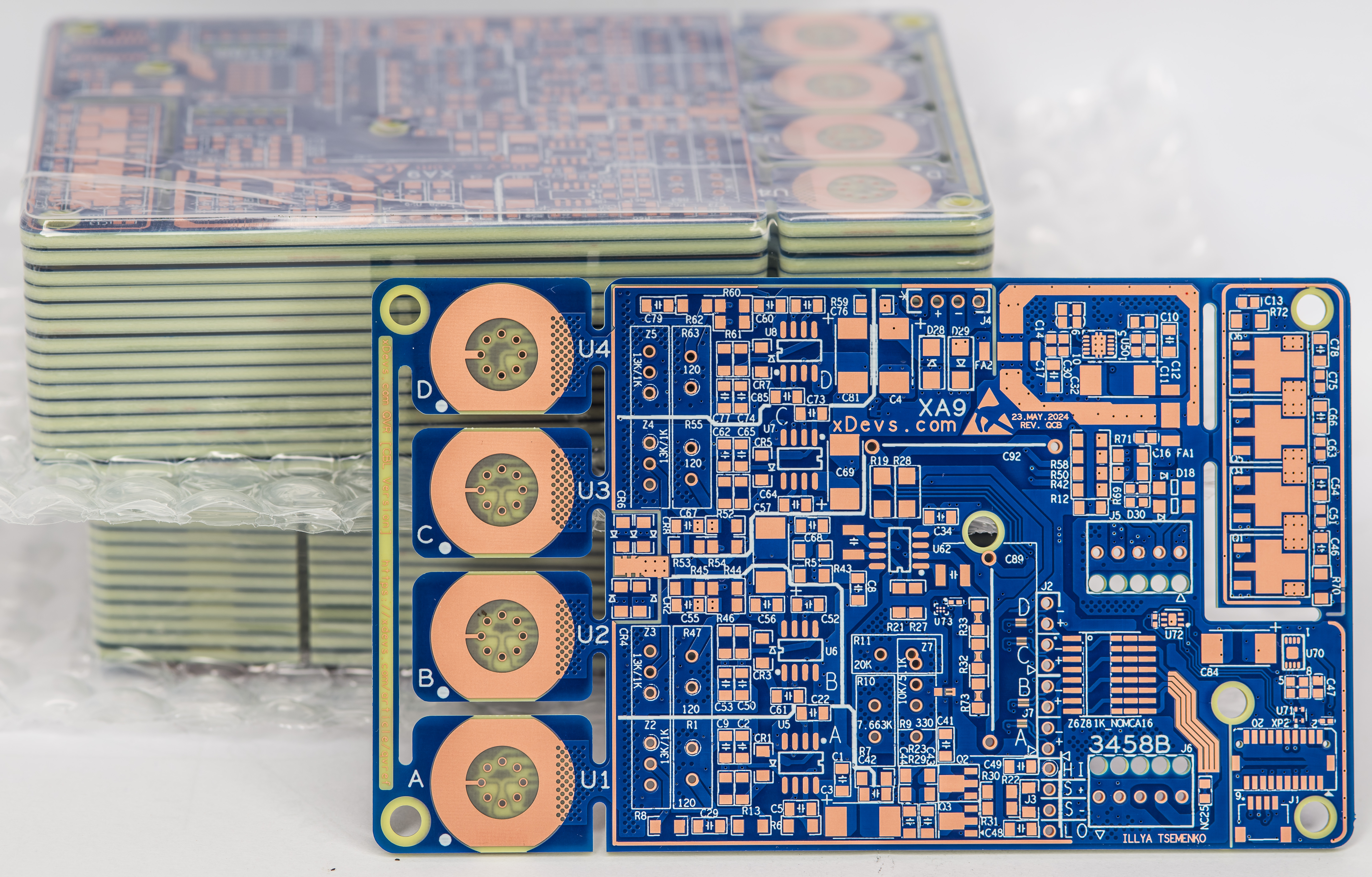
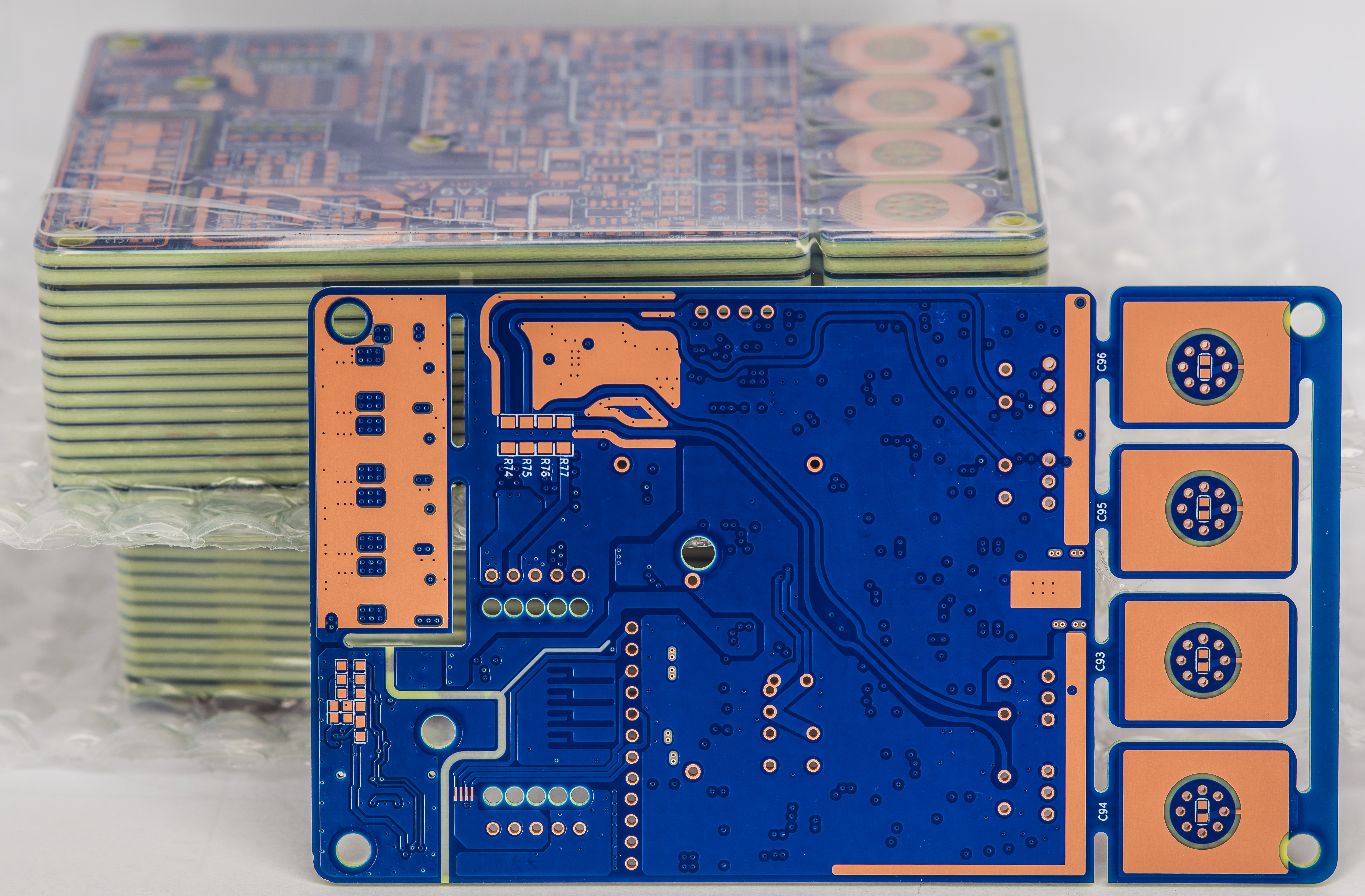
There are no more cutout slots around averaging resistor network pins and additional footprint for the bandwidth limitation capacitor behind LTZ/ADR chip footprint. Some of the ground plane pours were also changed in this design iteration.
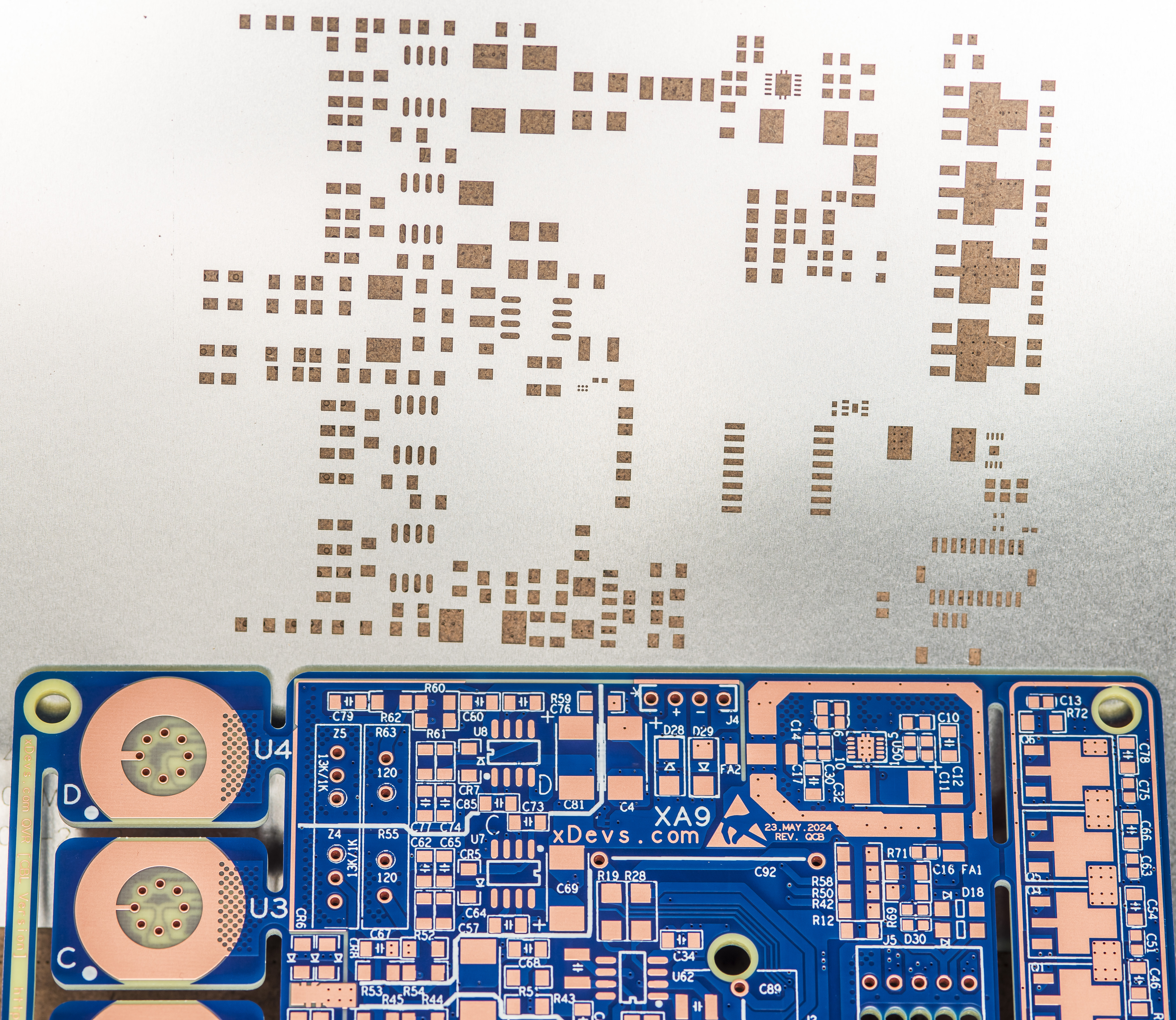
To help with assembly and soldering boards came with paste layer stainless steel stencil. This will allow me to use reflow oven to get all the non-critical SMT-type components soldered to PCB. Critical temperature sensitive components like metal foil resistors, zener chips and connectors will be populated by hand with my ERSA ICON iron.
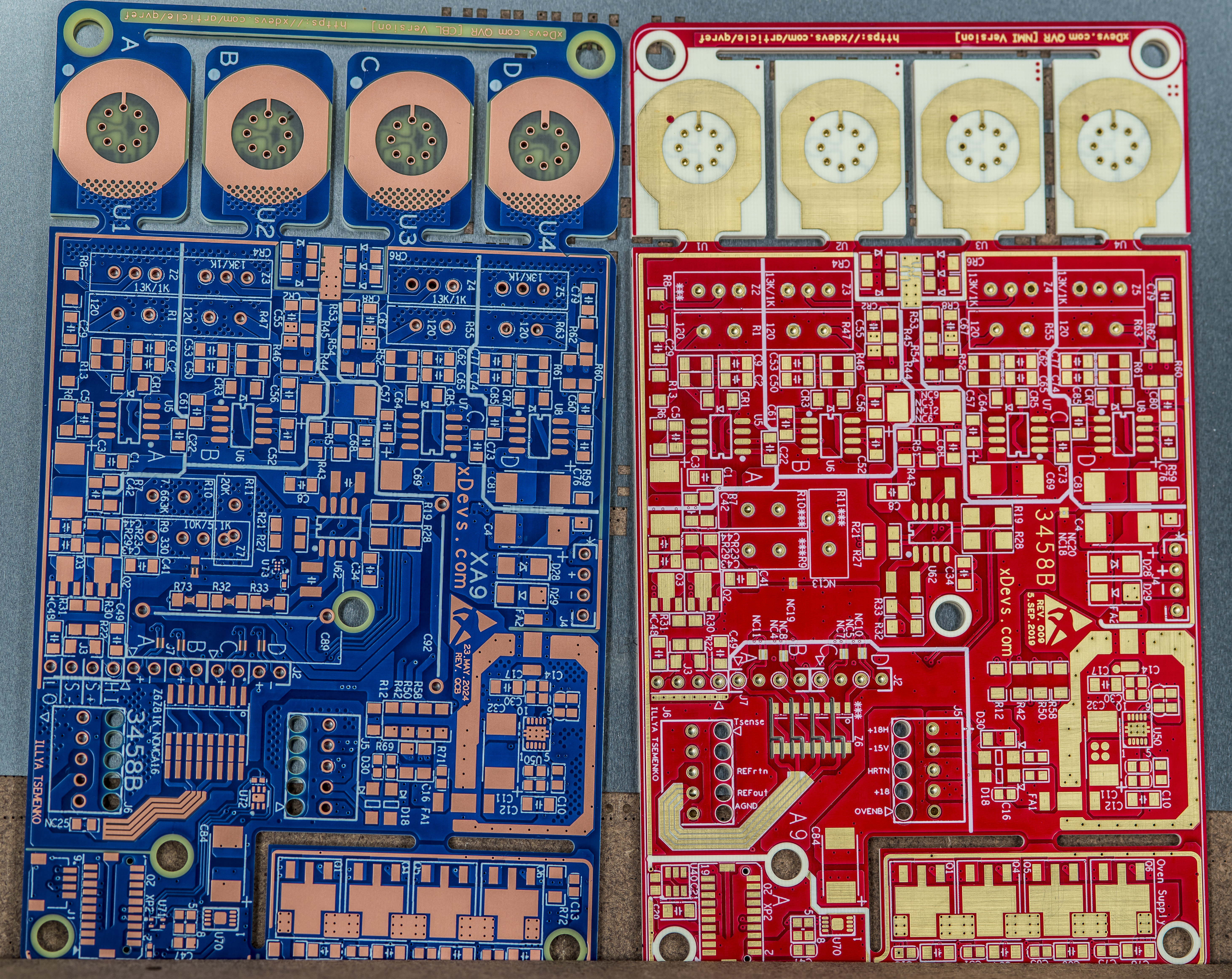
Comparison photograph of new Rev2 board (blue on the left) and older Rev1 (red on the right) shows the appearance and top layer differences.
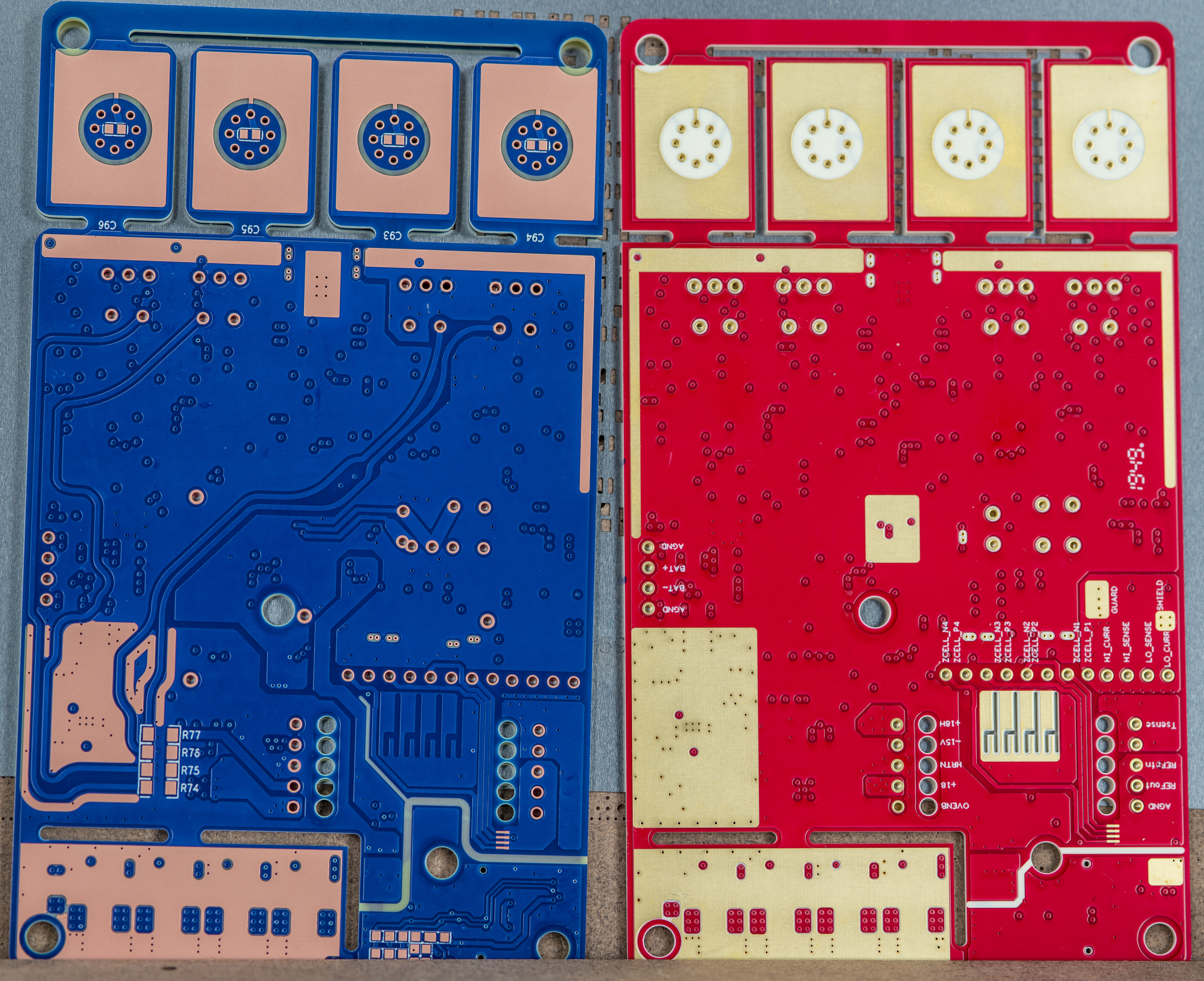
Similar comparison photograph of new Rev2 board (blue on the left) and older Rev1 (red on the right) done for the back side. Some optional passive components also placed on the bottom side for internal future testing.
New PCB is now 0.4 mm thicker due to different stack-up and metal thickness.
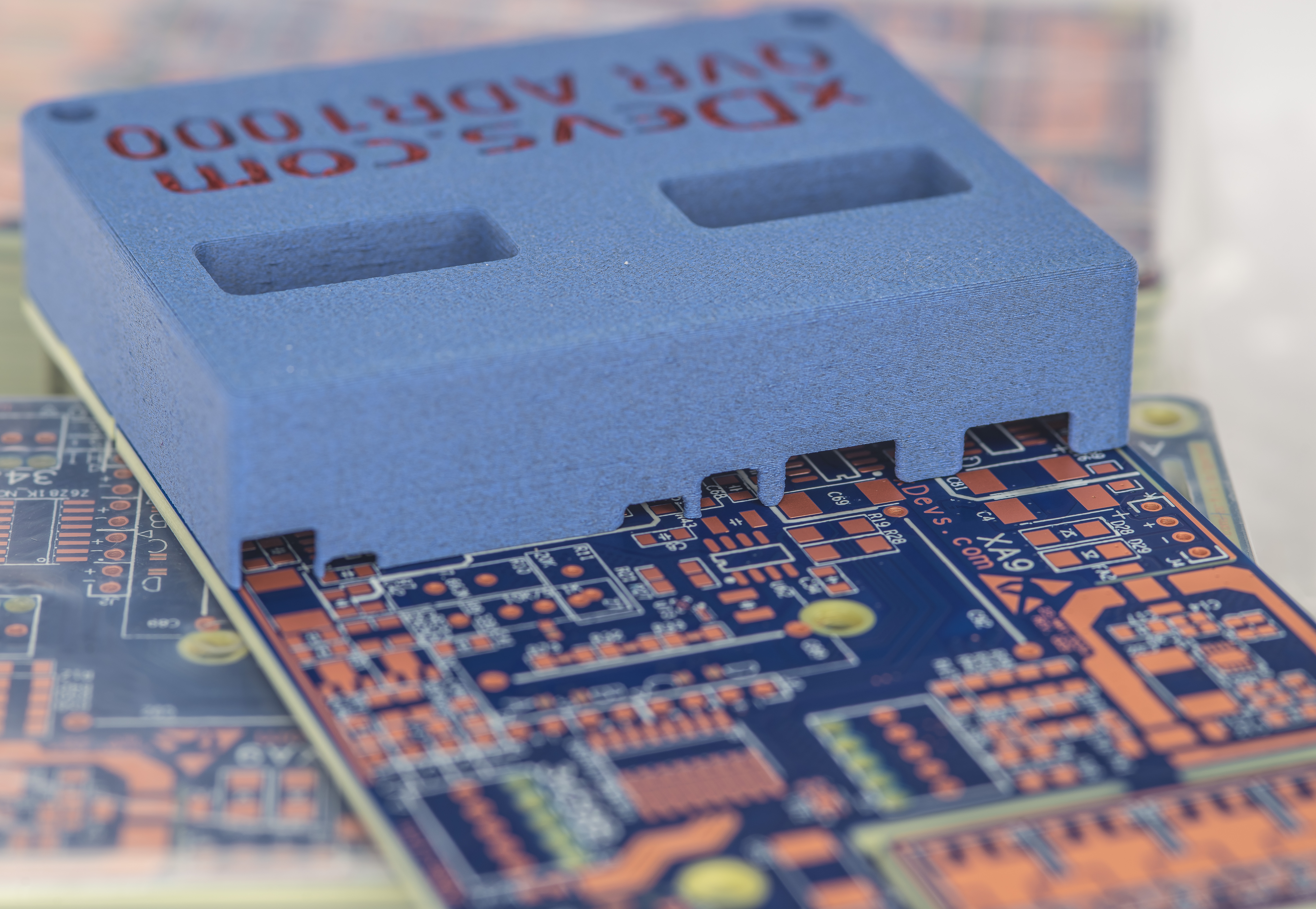
Plastic air cover shield is designed to fit across all reference IC pockets and each cell active circuits. Opening for each VPG resistor provided for reduced assembly height.
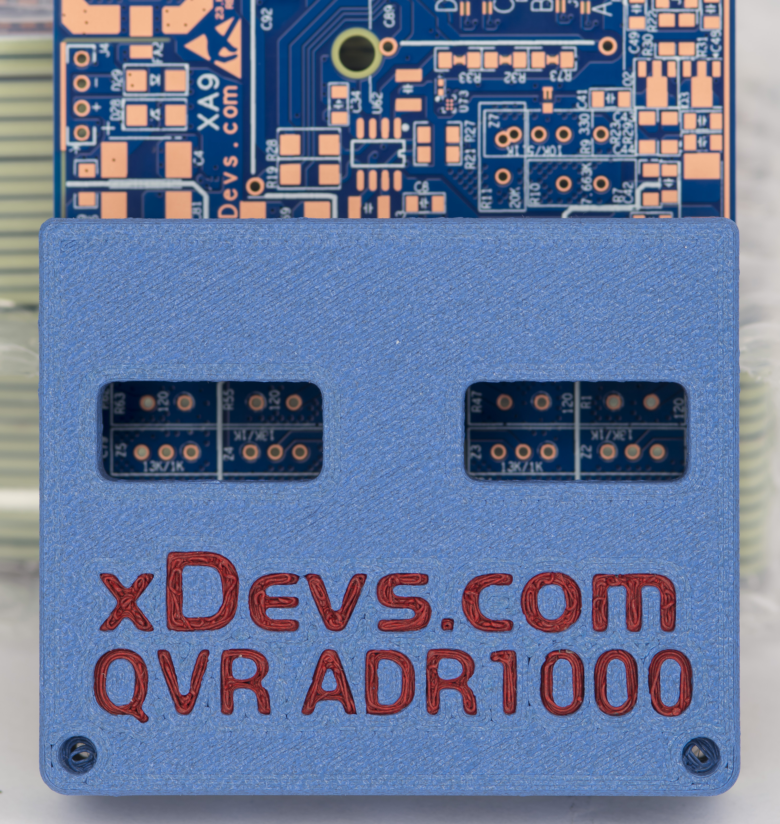
Cover is 3D-printed with blue PLA-CF filament using 0.15 mm layer thickness. It matches color of the board solder mask nicely :)
This cover also have special clearance cutouts for the tall onboard components such as 7343 tantalum capacitors. Otherwise the cover fully enclose each cell electronics from rogue external airflow.
Once I have few boards assembled, more photos and updates might be published later on.
SN0021 – Updated revision 2 QVR module with LTZ1000CH
This board is pretty much just an LTZ1000CH flavor of the SN0020 unit.
SN0022 – High power revision 2 QVR module with ADR1000
This board is similar to SN0020 but with power efficiency goals or power requirements sent to the trashcan. It’s power-hungry, hot and drifty, but hopefully very low noise.
Summary and conclusion
QVR project was quite interesting and fruitful learning device. I’ve learned and explored a lot of interesting performance aspects in multi-zener design arrangement and low noise voltage measurements. Quad LTZ1000A-based module was equal in noise to single ADR1000-based module, but with much better long-term drift.
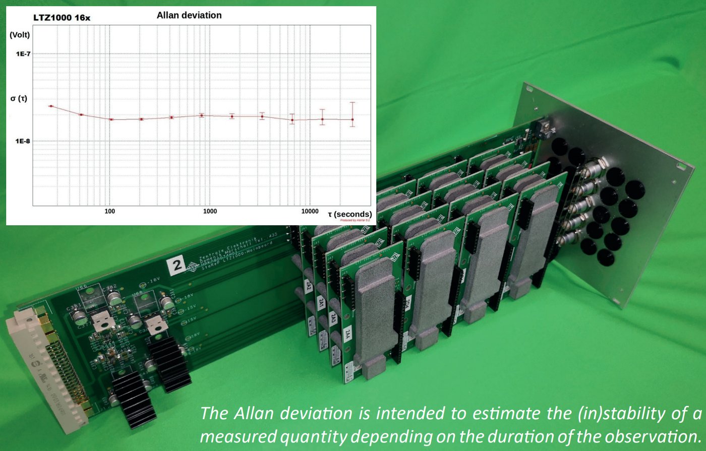
Ability to populate multiple independent reference cells on the same PCB and powered from same source provided nice and compact way to compare different chips and operating set-points. QVR is probably at the limit of what is economically hobby-friendly as a zener-based DC reference module, but there is still room to grow in future. For example, STAREP voltage reference cluster by Christine Böhm dissertation already demonstrated use of 16 LTZ1000-references to obtain very low noise DC output for physics metrology application.
Real-time discussion about this article and related stuff is very welcome at our own xDevs.com IRC-chat server: xdevs.com (standard port 6010, channel: #xDevs.com). You are also welcome to reach out via more traditional means
Projects like this are born from passion and a desire to share how things work. Education is the foundation of a healthy society - especially important in today's volatile world. xDevs began as a personal project notepad in Kherson, Ukraine back in 2008 and has grown with support of passionate readers just like you. There are no (and never will be) any ads, sponsors or shareholders behind xDevs.com, just a commitment to inspire and help learning. If you are in a position to help others like us, please consider supporting xDevs.com’s home-country Ukraine in its defense of freedom to speak, freedom to live in peace and freedom to choose their way. You can use official site to support Ukraine – United24 or Help99. Every cent counts.
Modified: June 23, 2024, 7:32 a.m.