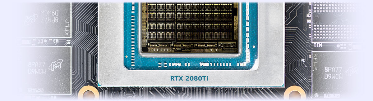
Image 2: RTX 2080 Ti introduction
Contents
Intro
In September 2018 the new generation of graphics chip was released by NVIDIA. Unlike many years of previous graphic card iterations, Turing architecture is the first design that marketed as realtime raytracing capable solution. Raytraing is very compute-intensive task to provide realistic lighting physics and rendering photography quality images.
This technology familiar to us in amazing big dollar VFX effects in creative clip-art and cinematic movies. Process of creating such photorealism usually involve large and expensive rendering clusters with hundreds of CPU/GPU cores sweating many GHz×hours to produce each ray-traced image frame. Hopefully, few years from now NV’s new technology implemented in RTX series will be picked up and adopted widely in the software industry to bring realtime raytraced rendering. NVIDIA released this hardware platform little earlier in form of Quadro RTX 8000 which sells for $10K USD and feature fully-enabled Turing TU102 silicon. RTX 2080 Ti is at core same card, minus the nerfed shader block and less VRAM capacity by disabling one of 32-bit memory sub-channels channel and different driver/support model. Quadro RTX also using higher density RAM chips to get more framebuffer capacity.
Now we have this technology is far cheaper GeForce branded device, so it’s time to take a look on EVGA GeForce RTX 2080 Ti XC ULTRA.
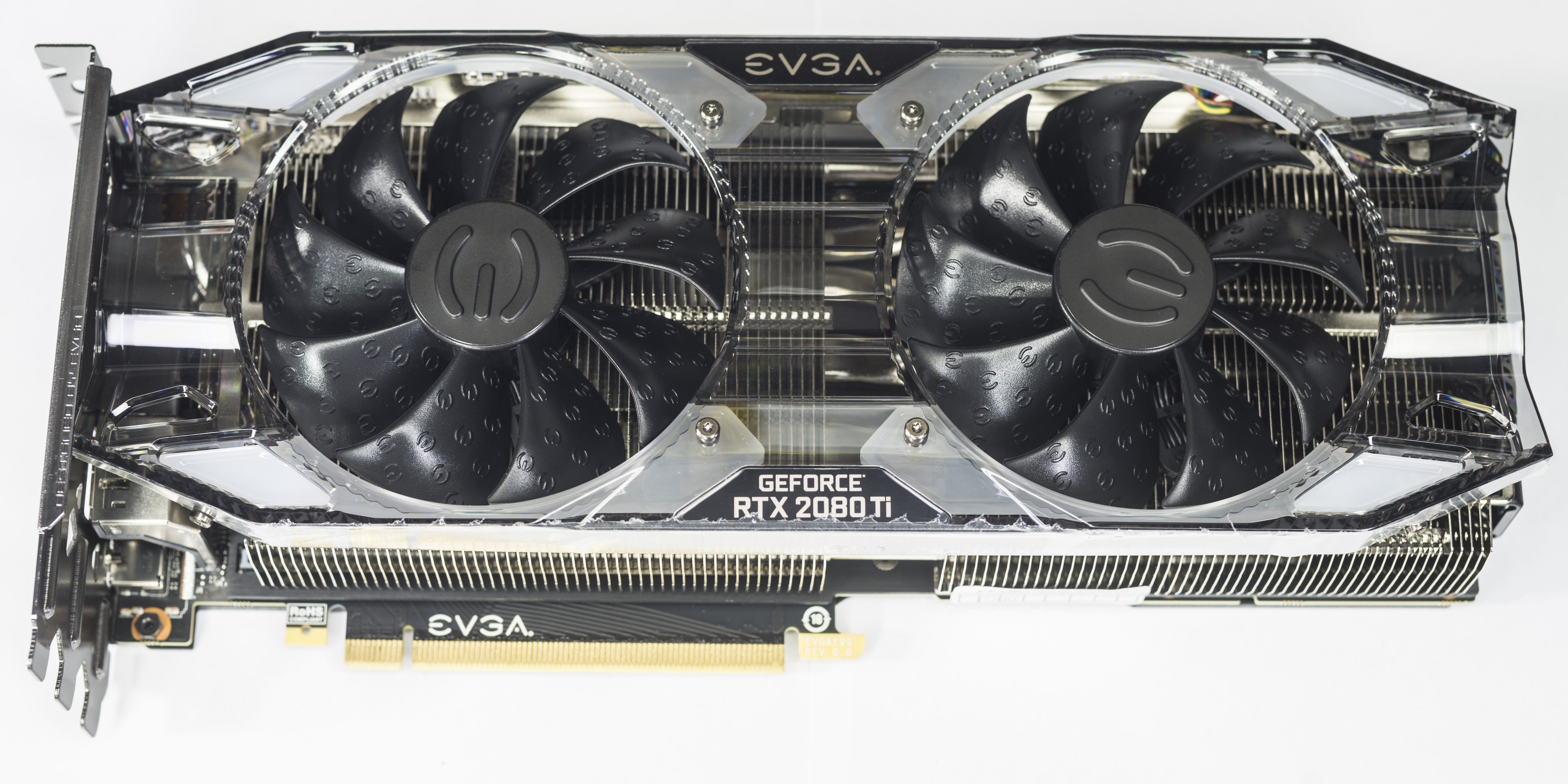
Image 1: EVGA RTX 2080 Ti XC Ultra graphics card
But this article is not a review and we will not be talking here about frames per second or performance points in 3D applications and games. You can find plenty of reviews online already. Here we will take screwdriver, soldering iron and take EVGA GeForce RTX 2080 Ti XC card apart to study its inner workings.
TechPowerUp’s GPU-Z since version 2.11.0 supports Turing RTX cards, displaying all key information about the installed device.
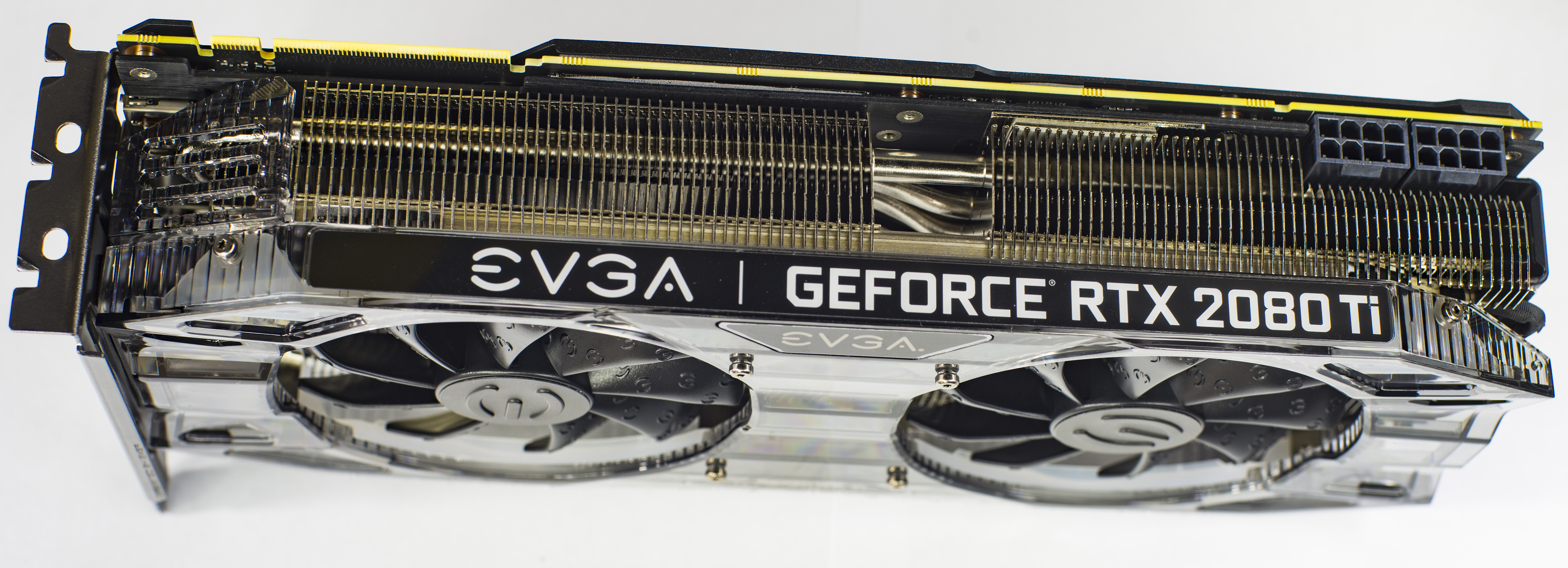
Image 3: Front side of the EVGA RTX 2080 Ti XC Ultra
If you interested in more usual “uncork series” for previous generation cards, check them here:
- Extreme OC Guide for EVGA GeForce GTX 1080 Ti K|NGP|N Edition graphics card
- Review of NVIDIA Titan V design article
- Reference GTX 1080/1070 – Uncorking Pascal
- Removing power limits on any NV card
- Dedicated EVGA EPOWER V DC-DC power regulator for VGA OC
- Using Raspberry Pi to control your VGA EPOWER VRM
- EVGA GTX 980 Ti K|NGP|N OC Guide
- Reference GTX 780/780Ti – Big KEPLER
- EVGA GTX 680 Classified – Uncorking guide
- Reference GTX 680 – Uncorking KEPLER
All FE designs for this GPUs are manufactured and sold directly by NV. Unlike top-end TITAN series, there are also multiple versions and custom designs built by EVGA, and one of these we will be looking at today here, XC ULTRA. This SKU is based on reference design PCBA, but with custom ICX2 fansink to provide better thermals.
As usual, you are on your own alone, even when doing even little simple mods. If you card/system bursts in flames or just simply stop working due to disassembly damage or user error, do not try to RMA it or expect a support from manufacturers. Anything below this paragraph in this article is NOT covered by any kind of warranty, and provided AS IS only for education purpose, without support from manufacturer or NVIDIA. So yes, “don’t try this at home”. Any RMA attempt of soldered card is easily diagnosed today and will be rejected.
No doubt, modifying your GFX for benchmarking and records require bit of above-minimal soldering skill knowledge cold mind and sharp eye. Entry-level things, such as how to probe voltage/resistance with multimeter, what is trimpot and how to solder piece of wire, as these things were explained over the internet thousand times already and easy to google. If you need more info – also check previous guides, linked above.
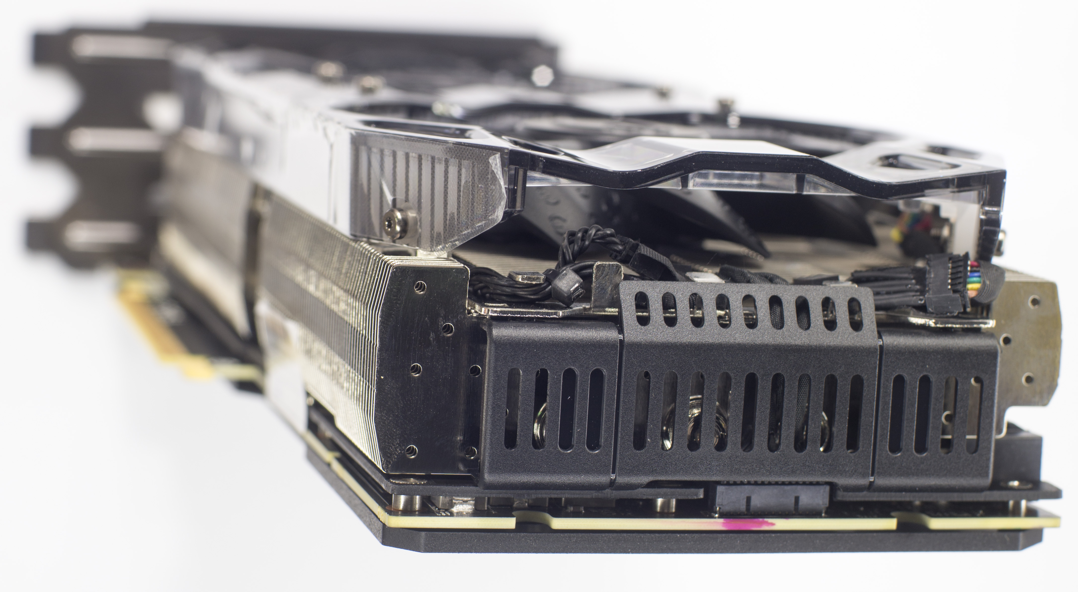
Image 4: Rear side of the EVGA ICX2 fansink with protection cover
“Ultra” version have 2.75-slot fansink, as new RTX chips provide new challenges for thermals and power managment.
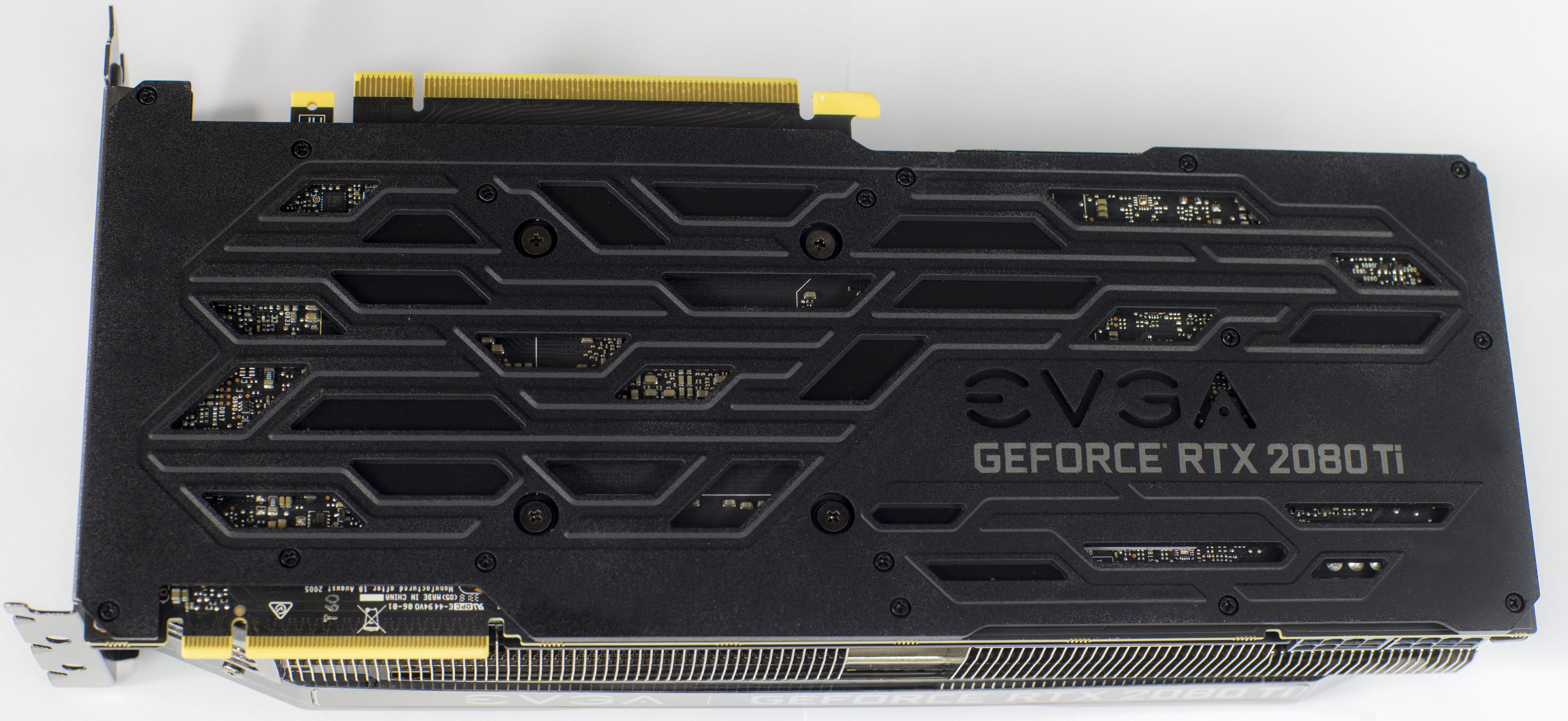
Image 5: Protection and improved cooling by aluminum baseplate
Disassembly is simple, just remove mount screws on backplate and I/O bracket that hold fansink, front PCBA baseplate and backplate all together. EVGA standard warranty conditions do allow fansink replacement with compatible watercooling solution, provided that no mechanical damage done by user during the disassembly/installation.
All plates have thermal transfer pads with plenty of area between all the plates, to keep heat distributed across wide area. This is important to keep VRM, memory and onboard components cool, while providing efficient cooling for GPU core by main finned cooling assembly.
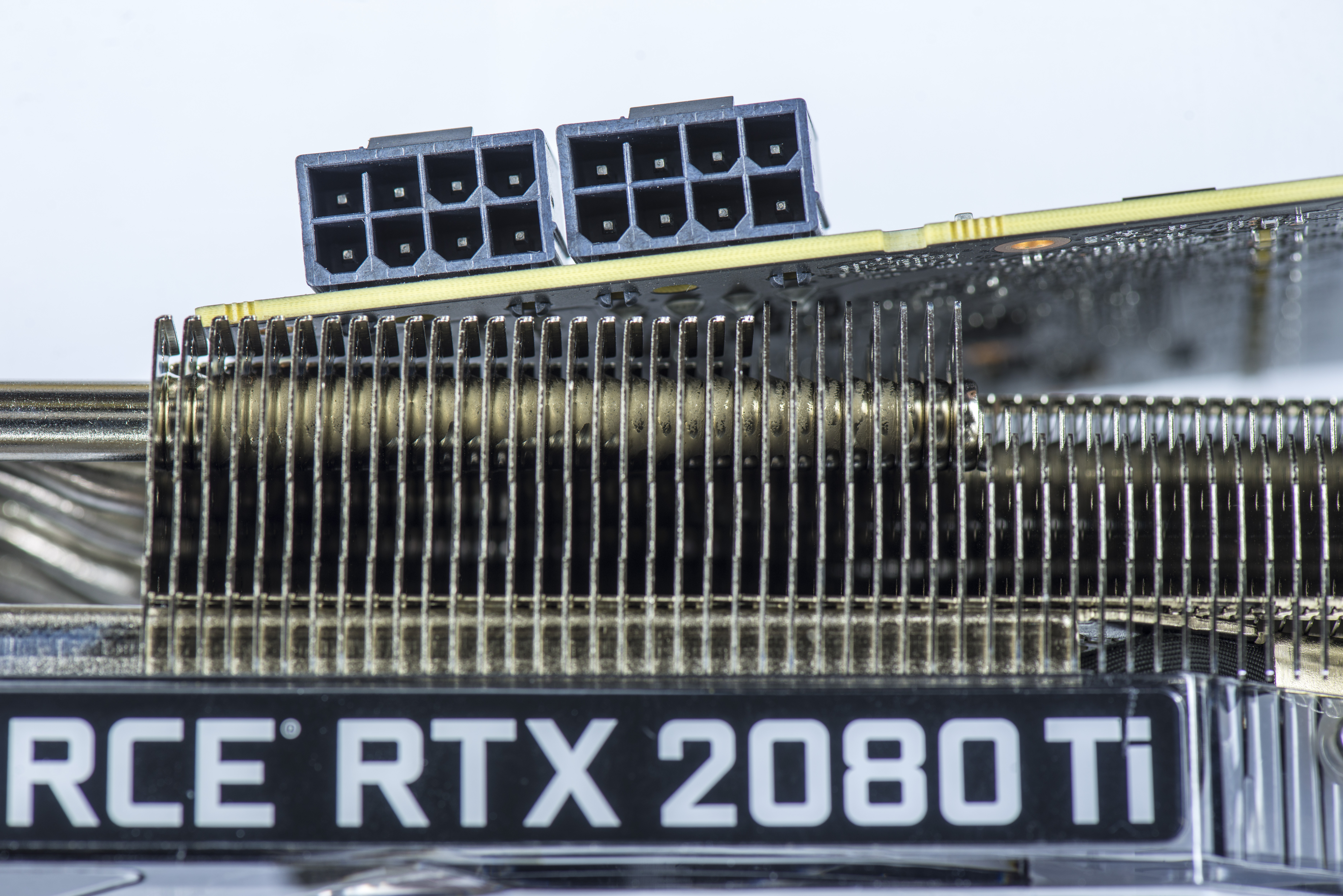
Image 6: Dual 8-pin MiniFit-JR +12V power entry ports
This RTX 2080 Ti have both 8-pins located on top edge of the PCBA. These can provide plenty of power for any normal-condition benchmarking, stress-testing and overclocking.
There is common misunderstanding to refer 6-pin or 8-pin MiniFit.JR connectors as fixed 75W or 150W power capable inputs.
Nothing can be further from truth actually, as connector port itself does not define the power cap. These power levels are nothing but just the way for how NV determine capability of used board hardware to deliver high power to the voltage regulators. It’s purely imaginary specification and have nothing to do with actual power taken from connector nor power input capability. Active circuitry on PCBA after the connector is used to measure current flowing from the connector into the VRM. This enables software, driver and NV BIOS to handle GPU clocks and reduce voltages if measured power hitting programmed BIOS limit value (which can be lower or higher value than 75/150W!).
So if we play and change circuit to adjust the calibration point, this limitation will be lifted accordingly as well. Also to make sure we are not at any physical limit of power connector itself, check Molex 26-01-3116 specifications, which have specifications both 13A per contact (16AWG wire in small connector) to 8.5A/contact (18AWG wire). This means that using common 18AWG cable, 6-pin connector specified for 17A of current (3 contacts for +12V power, 2 contacts for GND return, one contact for detect). 8-pin have 25.5A current specification (3 contacts for +12V power, 3 contacts for GND return and 2 contacts for detection). This is 204W at +12.0V level or 306W for 8-pin accordingly.
Now when somebody tells you that 6-pin can’t provide more than 75W, you know they don’t understand the topic very well. It’s not the connector itself or cable limit the power, but active regulation of GPU/BIOS/Driver according to detection of used cables and preprogrammed limits. So how actual power measured? Will see later on detail shots of the RTX 2080 Ti PCBA.
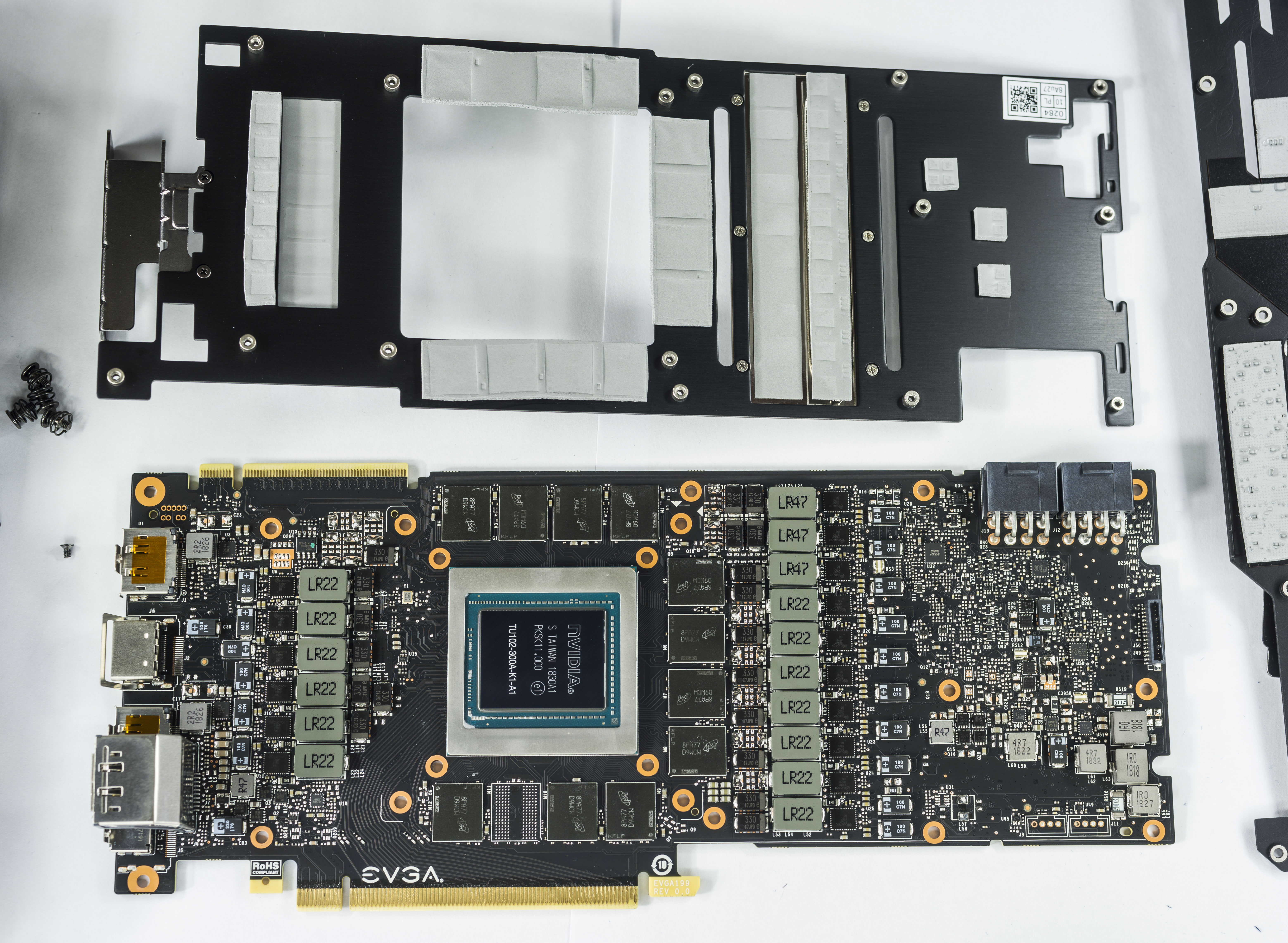
Image 7: EVGA RTX 2080 Ti XC Ultra in it’s bare PCB glory
Overall PCBA design is similar to old GTX graphic cards, except the rotation of GPU+DRAM section and new power solution. Display output connectors are located on the left edge. DVI-D port is well gone, replaced with tall full-size DisplayPort. All DisplayPort outputs are now compliant with version 1.4 of the standard, able to drive HBR3 data rates for 8K 60Hz display panels.
New display feature added on RTX – VirtualLink port. It is new interface (or yet another standard of already confusing USB family) aimed to simplify connection of the VR headsets, thanks to support of transferring USB3.1 10Gbps and DisplayPort 4-lane HBR3 at same time with up to 27 Watt of DC power using compact VirtualLink cable. Yes, normal USB Type-C will not work for this case. Mechanically this port is same as USB Type-C, but electrically it’s bit different.
Higher power demands of the new TU102 GPU are hinted by hefty power regulator, split into two sections on left and right sides of the ASIC, just like we saw before on Titan V teardown. There are no less than 13 phases for core logic power and 3 phase power for memory.

Image 8: GPU and 11 GBytes of GDDR6 14 Gbps rated memory. Image rotated for clarity.
GPU bears TU102-300A-K1-A1 marking, which tells you about 102 type high-end series processor (to remind you, GTX 1080Ti based on GP102, Quadro RTX 8000 have same TU102 type GPU and Volta cards equipped with GV100), silicon revision A1. It was manufactured by TSMC fab in Taiwan. Large set of tiny 0201 and 0204 decoupling ceramic capacitors around GPU die to help with power delivery surges and transients. No hidden jumpers, traces or test points are visible on the package elsewhere. All modern GPUs and CPUs using electrical on-die fuses that accessible only by top secret factory test equipment, so there is no hope of any kind unlocking by end users (or AIB vendors).
Usual dual SLI HB connectors are now gone, replaced with single NVLink 2.0 ×16 lane edge port. While NVLink on RTX 2080 Ti is based on same enterprise Tesla interconnect, it is not compatible and allow only direct link between two cards. NVLink interface using SERDES and serial differential pairs, similar to more usual PCI-express Gen3 but with higher bandwidth speeds and own protocol. Lots of bandwidth enable memory sharing to combine VRAM on each RTX card into one larger framebuffer, available to both GPUs. Will see how that scales in real-life performance numbers, when SLI performance numbers surface in reviews.
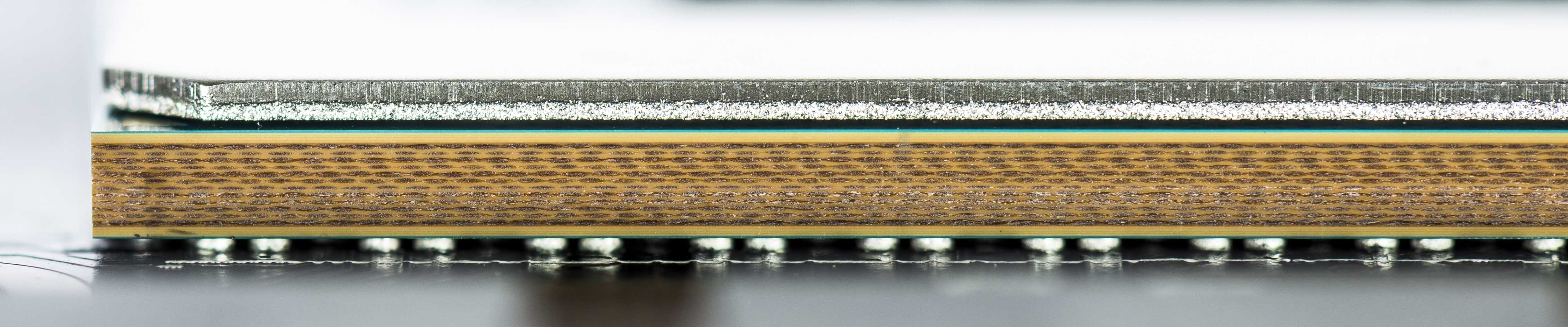
Image 9: Turing 102 side BGA substrate photograph, showing package material stack layers
NVIDIA TU102 package substrate that fanout large silicon die for PCBA interconnect using at least 16 internal layers, but physically package is using same size ball array as GTX 1080 Ti. There is no need for advanced packaging or silicon interposer like on Volta or Pascal-generation Tesla, so this GPU is cheaper to package.
Due to closer GDDR6 positioning and higher speed routing mounting holes have changed location vs 1080Ti. Yes, this card is not compatible with older 10 and 9 series GTX extreme cooling coolers. You will need mount for LN2 containers that support Titan V / RTX series.
Main PCB is build using 12-layer stackup using halogen-free RoHS-compliant materials. It is less advanced than Titan V design, but still very impressive due to higher component density.
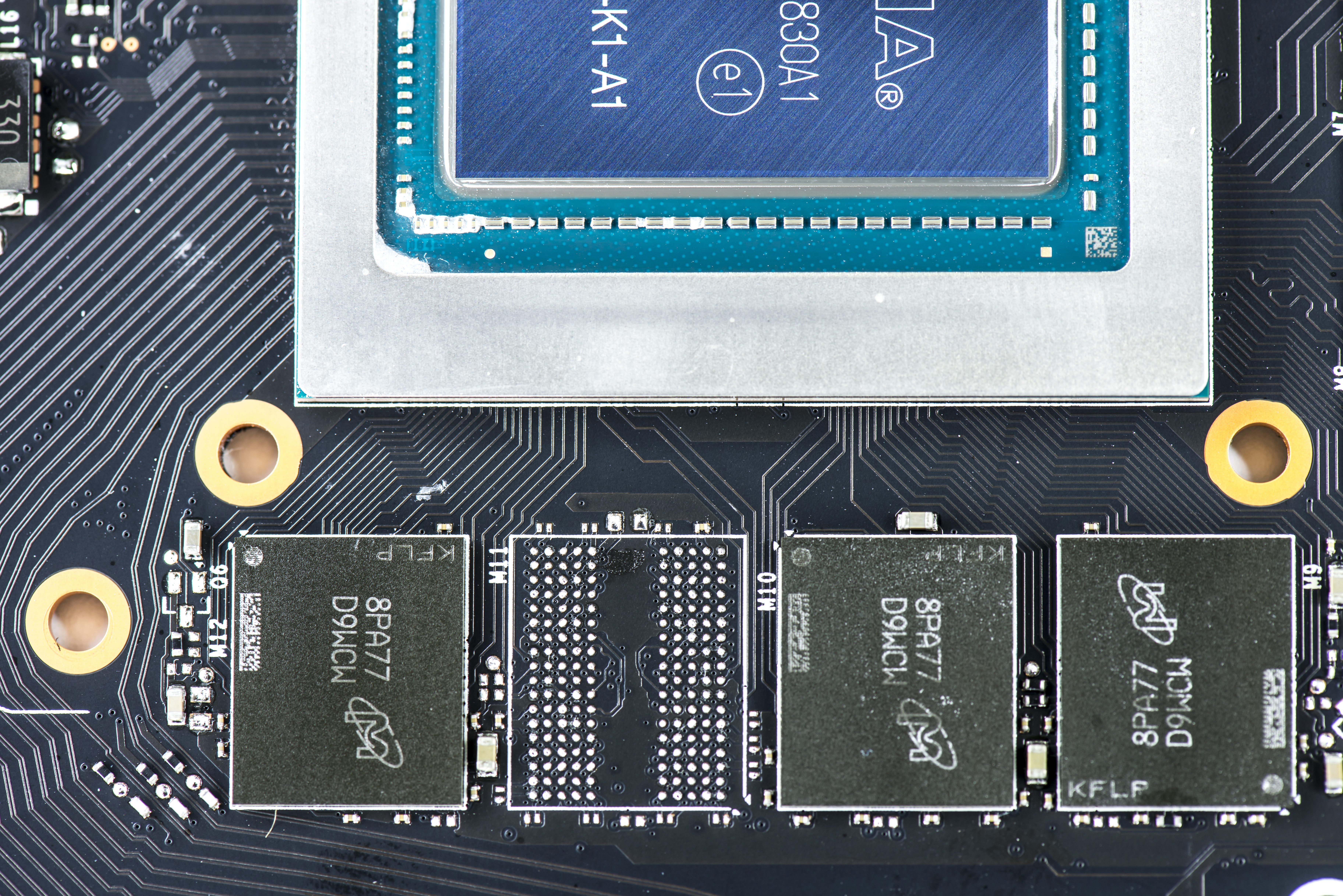
Image 10: “Stolen” memory chip for memory controller channel
Unlike Quadro RTX with TU102 core, consumer RTX 2080 Ti have disabled SMX block and related memory channel, limiting framebuffer capacity to “just” 11 GBytes. Micron memory is now GDDR6 type to give higher bandwidth at fraction of the HBM-type DRAM cost. Using Micron’s FBGA & Component Marking Decoder we can easily get chip part-number: MT61K256M32JE-14:A which according to datasheet is 8Gbit GDDR6 SGRAM with rated data rate at 14.0 Gbps, however even faster 16.0 Gbps chips are expected in future.
Other vendors like Samsung and Hynix are also making new GDDR6 memory, so eventually we will see more memory options across different 20-series RTX cards. Technically, this is QDR memory, but to keep things simple JEDEC desired to keep GDDRx name for it, as it’s layout and core technology is similar to well-known GDDR5.
Few more things we can learn from the memory IC datasheet, such as same nominal voltage as GDDR5X – 1.35 VDC plus pump level voltage VPP with 1.8 VDC spec. Maximum specified voltage for memory core is 2.0 VDC, however we would not recommend going THAT high :).
Design overview
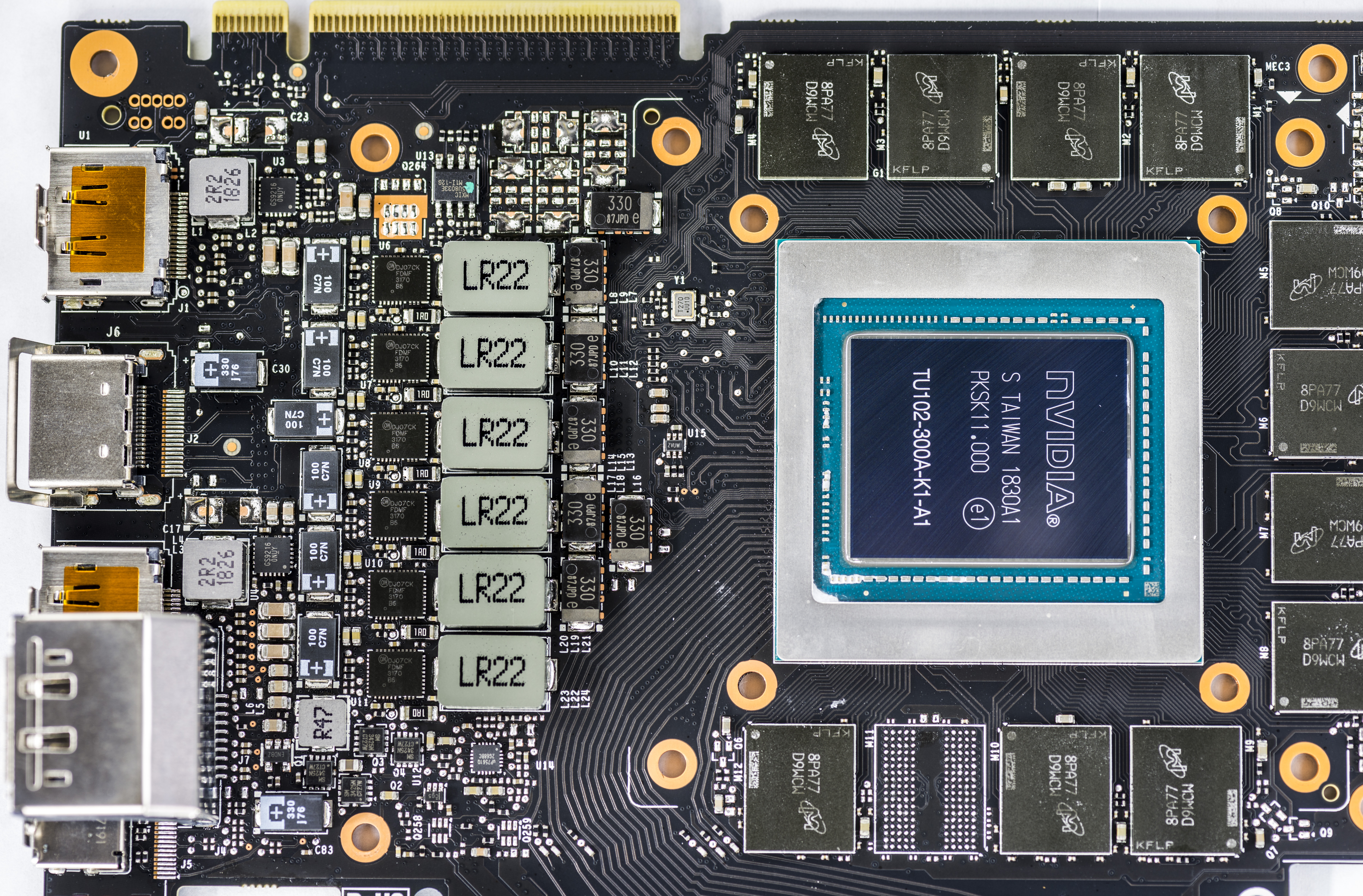
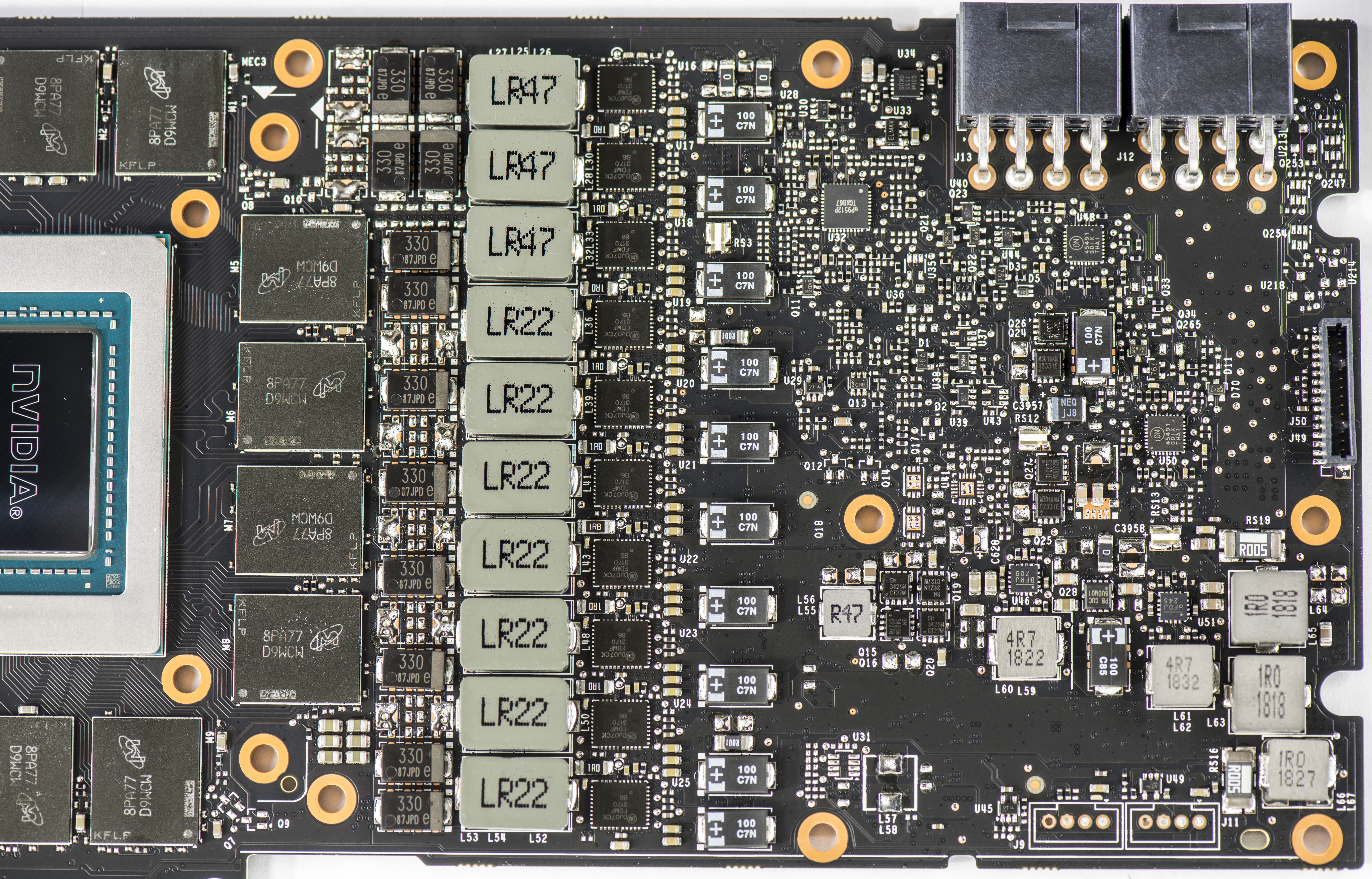
Image 11-12: Close-up photograph of the card’s front side
Power regulator on the card is very similar to one used in Titan V, so we suggest to check some mapping here to refresh memory.
One of significant changes – good old INA3221 current sensor IC we all know from years of GTX cards now got replaced with 4-channel ON NCP45491.
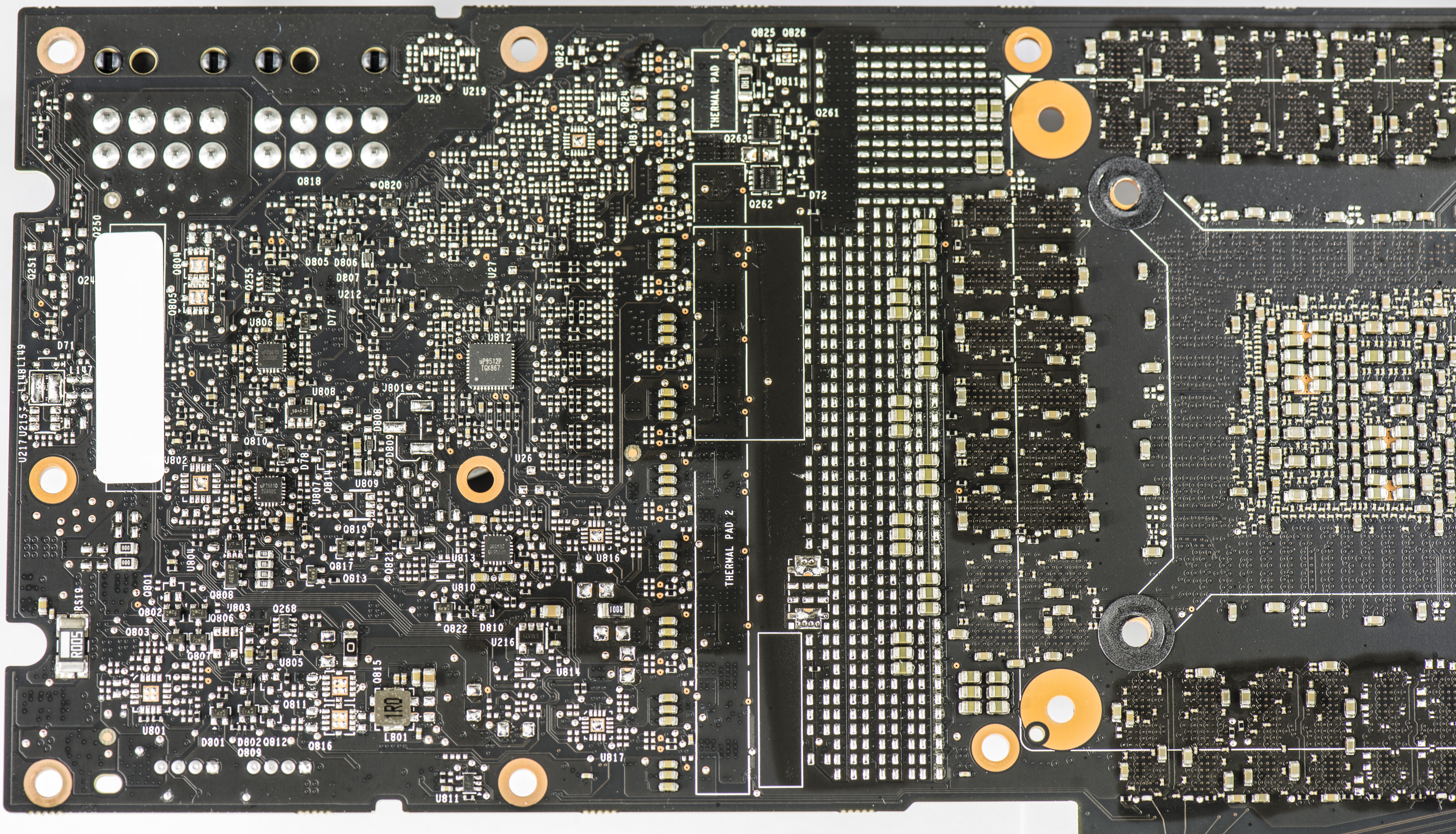

Image 13-14: Close-up photograph of the rear side
GPU backside decoupling now have myriad of smaller 0201 ceramic capacitors. PCIe routing wiggle it’s way to the connector around the memory chip area. Lot of unpopulated spots behind the power regulator output area is reserved for 0805 size MLCC’s. Perhaps fully featured card, like Quadro RTX have more of those populated to cope with increased power requirements of fully enabled GPU and large memory buffer.

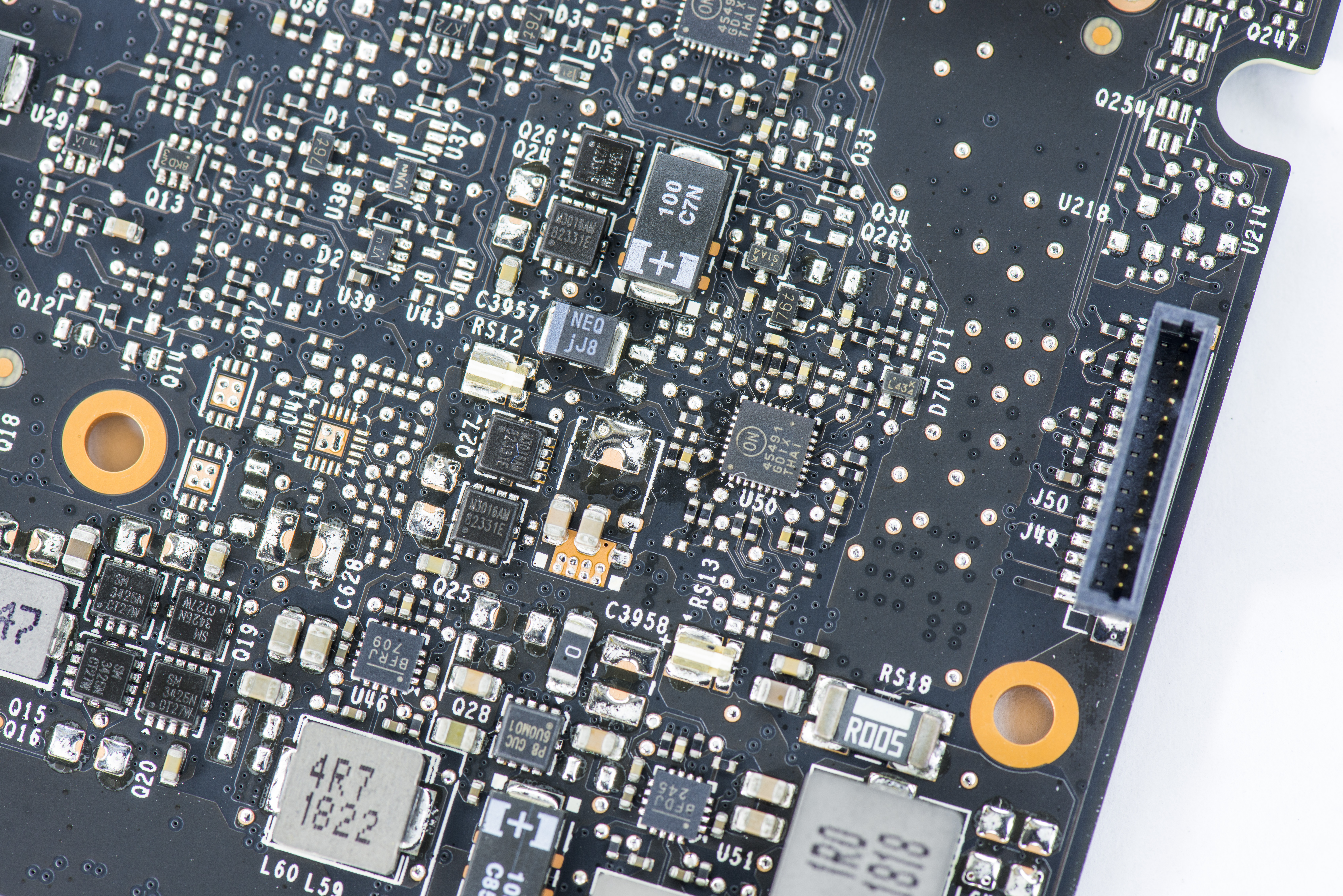
Image 15-16: Power components near the display I/O and new RGB-enabled dual fan header.
Left side VRM is tightly packed with 6 x NVVDD high-current phases, with remaining 7 phases on the right side. Memory is powered by 3 x FBVDD phases. All input and output capacitors are SMT tantalum and ceramic type. Inductors for core power are 0.22 µH (marked LR22 on this card), while memory power is 0.47 µH (marked LR47). U13 chip with green paint dot is BIOS SPI ROM.
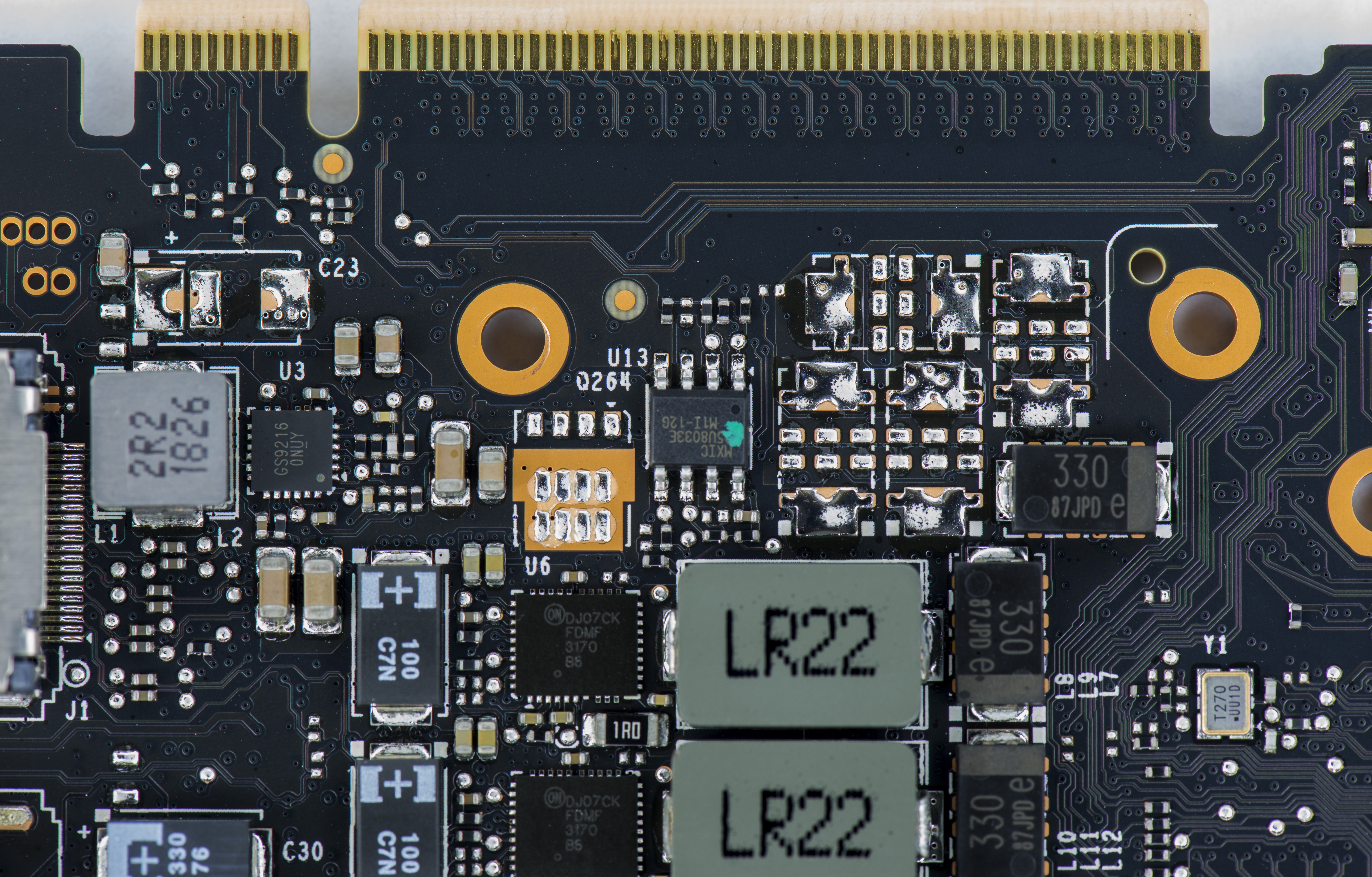
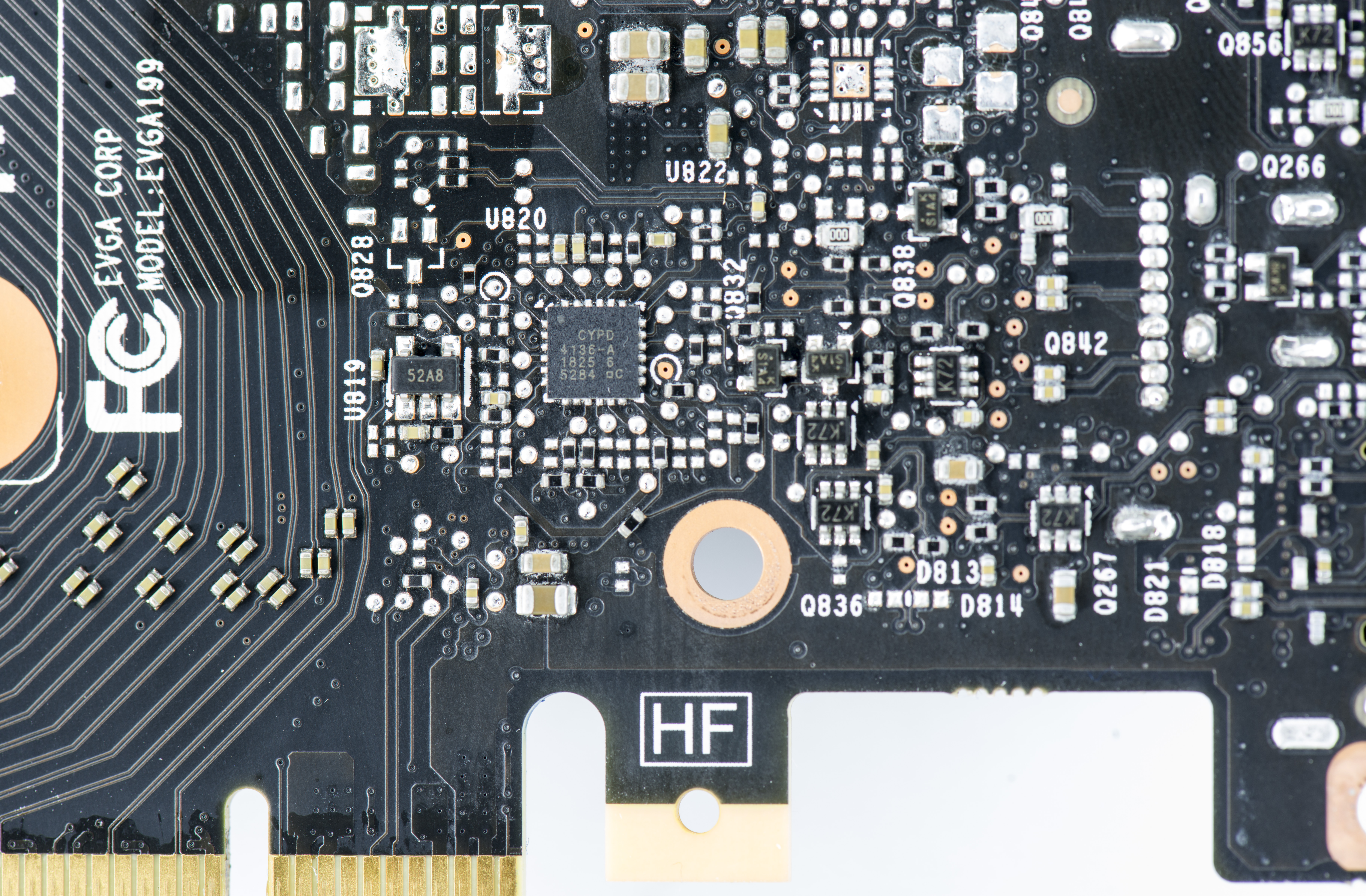
Image 17-18: Close-up on NVLINK edge connector and VirtualLink/USB Type-C controller
Voltage monitoring points and mods
Will need set of common tools for successful modding of this reference-based 2080 Ti, which is similar to any other VGA.
- Card itself. Brand new EVGA GeForce RTX 2080 Ti XC ULTRA used here.
- 2 × 100 KΩ multi-turn VR (trim pot) for mod.
- 3 × 5 Ω chip resistors, 0805 size. Example from Digikey, Mouser, Farnell DE for power limit mod.
- 25-45W soldering iron for trimpot mods.
- Roll of 28-32AWG insulated wire
- Soldering FLUX
- Kingpincooling TEK ICON container
- DMM (I use fancy handheld Fluke 87V and high-performance Keithley 2002, but any 10$ DMM can fit needs of this guide)
In this article, we used ERSA iCON-1 soldering station with to cover all below. 102CDLF2.4 tip covered all trimpot mods for this guide, with tip temperature set to 290 °C. Before starting with soldering, clean the usual mess on table, get all tools checked and ready, turn on enough lights to clearly see all those tiny parts on PCB. Worth to ensure enough space around, so you don’t knock other stuff by accident. Also worth to take a close look on PCB layout from both top and bottom sides, to get familiar with location of key components and design.
Also interesting to test our fellow overclockers, if they pay attention to our OC Guides. This modification will not have shown photos to baby-sit the modification steps. But guide does provide ALL the information necessary to perform successful modification.
STEP 2 – Get card ready
Remove backplate and cooler from the card, since access to both sides of PCB for all modifications is required. No special screwdrivers needed, just usual Philips will do just fine.
Keep all those custom screws in secure place somewhere, so you can put heat-sink back after you done. Remember, after soldering your warranty will be surely null and void, as every RMA center will easily see non-factory soldering specks, even if you very careful.
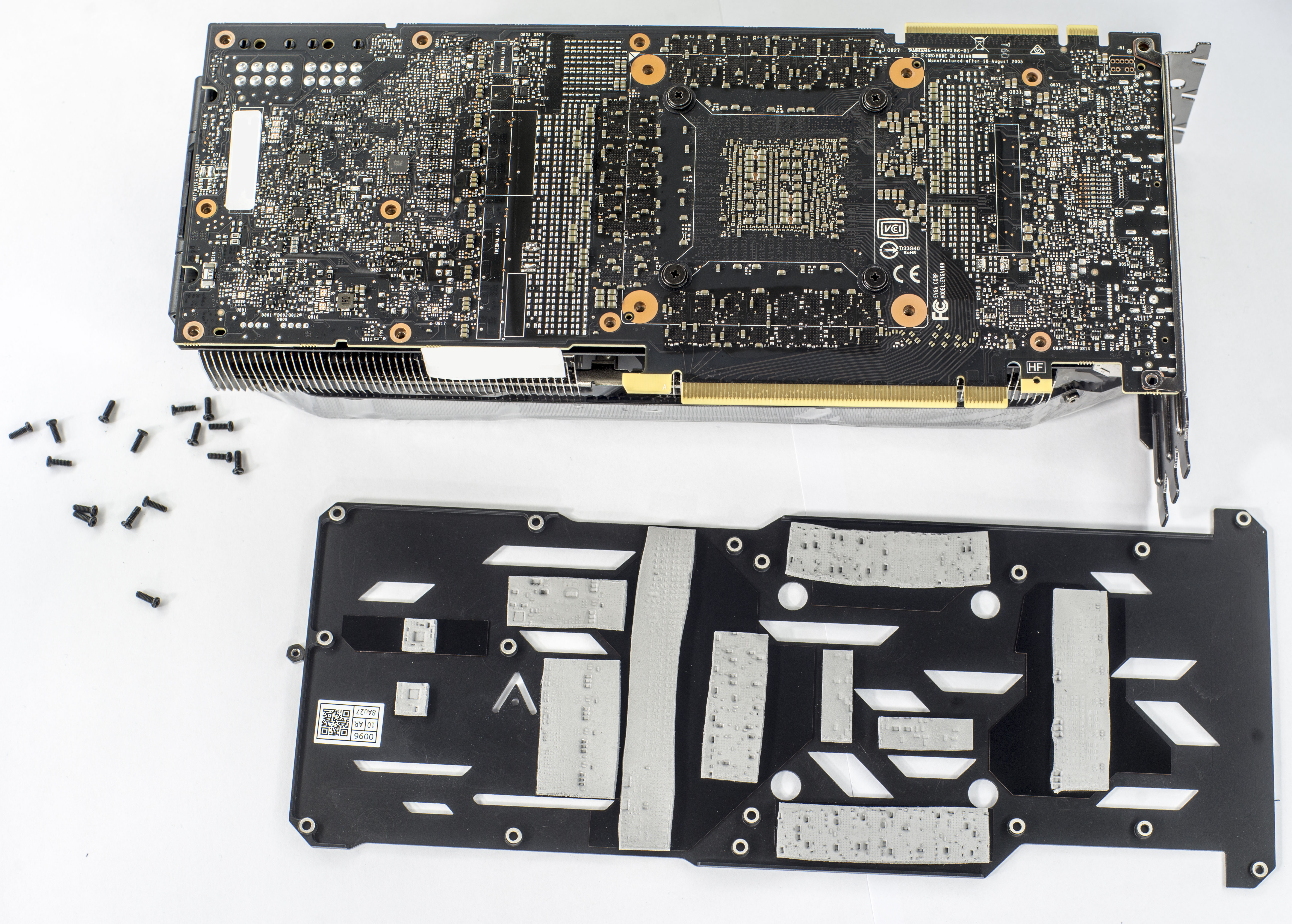
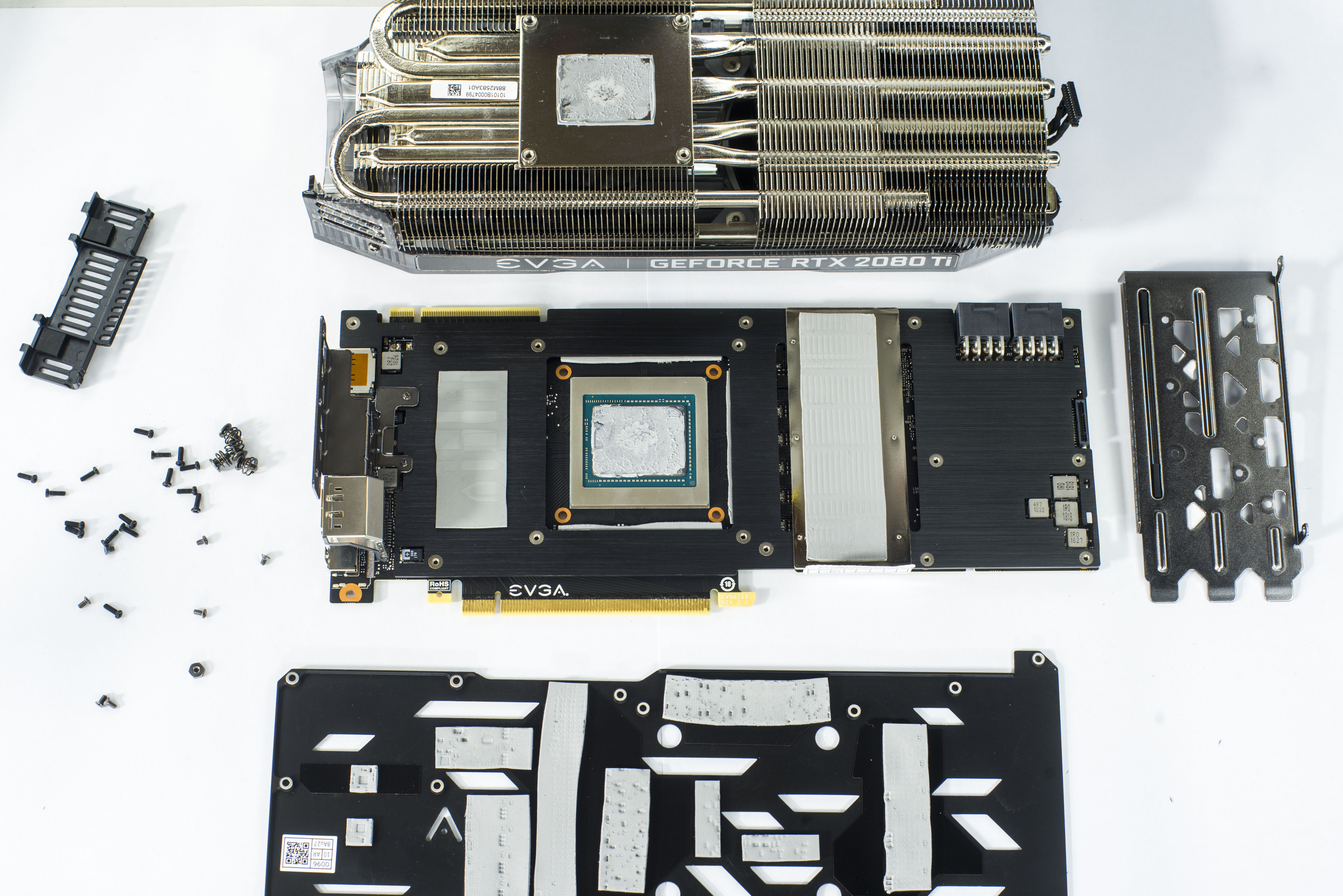
Image 19-20: Heatsink removal and naked board
Now graphics card is exposed and ready for some measurements and modifications. I’ll spare our readers from boring part of measuring various points to find out what we need and where different connections go, so we can jump right into good stuff, starting with removing power cap limitations.
STEP 3 – Power limit overrides
RTX 2080 Ti is heavily limited by the power. Nearly always, even with very good cooling card clocks will be governed by the power limiter, as this large GPU chip takes a lot of juice to operate. If you intend to do serious overclocking and benchmarking, it is paramount to trick power monitoring circuitry to report lower power reading, so you not run into power throttle (as much).
Just like previous guide about GTX 1080 FE card, idea and concept of the power mod is working same way. Old GTX cards used simpler well known Texas Instruments INA3221 sensor IC, which is triple-channel monitor able to measure voltage, current and power on +12VDC input rails using just few external components and current shunts. Current shunt is special type of resistor which generate little, but measurable voltage which closely depends on amount of current flowing thru it. Thus card can detect power consumption in real-time and adjust its clock speed and performance automatically to keep power within specified envelope.
New RTX 2080 and 2080 Ti cards use new 4-channel ON NCP45491. This chip also using current sense shunts to measure current flowing from the power supply connectors and taps the voltages for power calculation.
Related 5 mΩ shunts can be identified on front side of the PCBA by R005 marking. Two are located on the front side with labels RS18 and RS16, and one on the back side marked RS19. Sometimes there are no marks, but look is always very similar, like a large rectangular flat part with two or four wide metal terminals. Usually these shunts are located very close to input power connectors before the main VRM circuitry.
Few minutes with DMM probing will let you to trace connection for specific channel at NCP sensor U50 or U48 chip. I would suggest to draw the connections and involved circuits to NCP45491, taking block diagram schematics from datasheet as a guidance.
If we manage to reduce voltage signal (which is in linear dependence from current) from these shunts to NCP sensor IC, then reported power limit will be reduced as well. Don’t do anything with these shunts directly, just understand what they are for. Common “modifications” like applying liquid metal paste or using pencil are bad idea, as they do not provide reliable and static resistance change. Pascal, Volta and Turing cards have also protection against under-reporting, meaning that GPU will be stuck in low power throttle state if reported power is zero or below the minimum limit.
Adding 2-5Ω 0805 size resistor on top of every input sense pair next to related NCP45491 chips U50,U48 will reduce power levels, measured by NV driver/GPU. These chip resistors can be bought in usual electronics shop, or online at retailers like Digikey, Mouser. In worst case you still can use usual thru-hole resistor, but it’s not as convenient and you risking damaging caps or ripping traces off the board if you apply physical force on the joints.
I don’t show actual photo of this mod, as it’s nearly the same as in GTX 1080 case. This modification also very similar for all other NVIDIA cards, with bit more details covered here and here before.
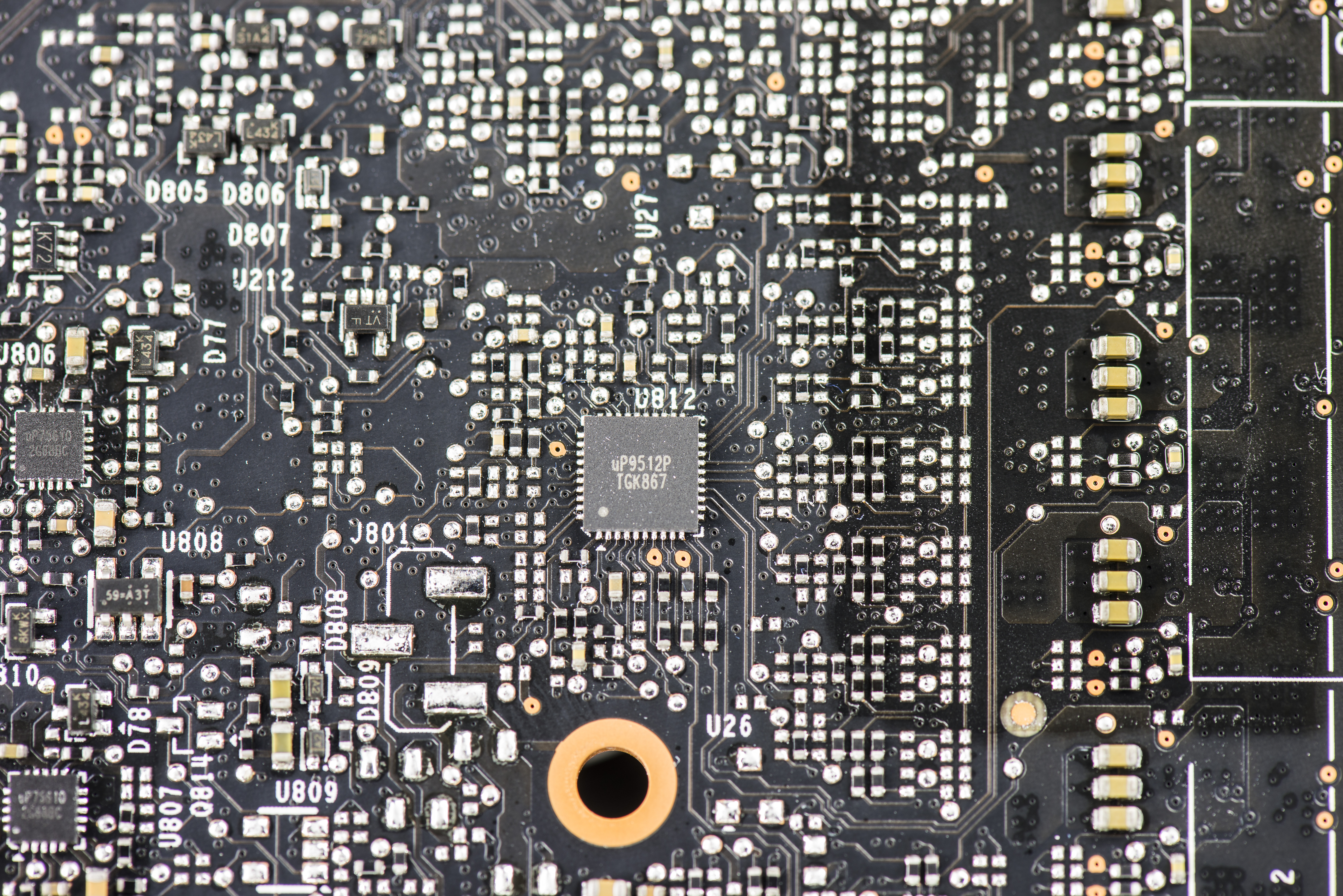
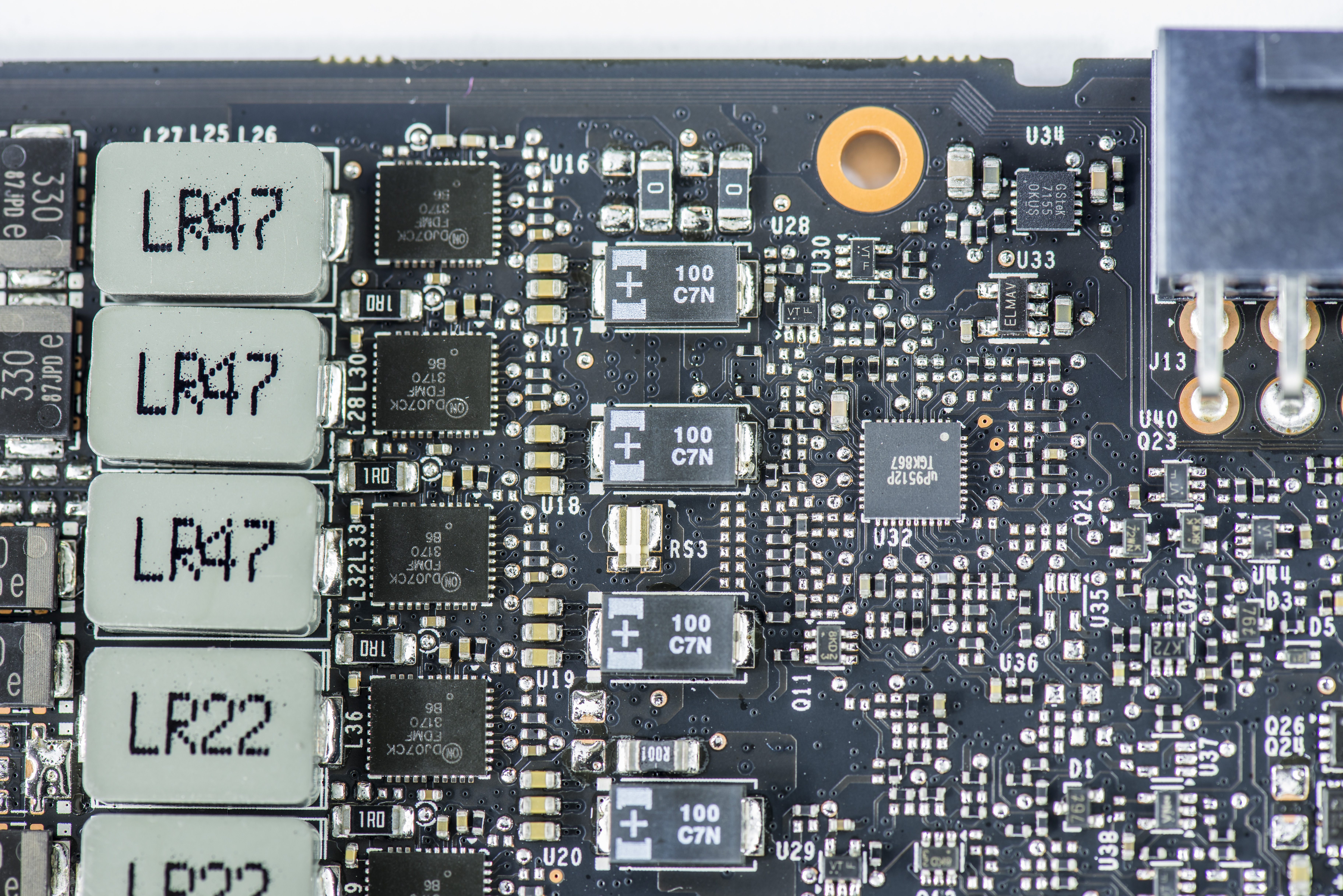
Image 21-22: GPU voltage and memory voltage controllers.
Now the important part. Power controllers for NVVDD and FBVDD are UPI UP9512P and voltage sense is pin 31. Trimpot mod can be applied in the usual manner to this pin. Best resistance to use is 100 KΩ, based on measurements on the our actual card. U812 handle core power regulator output and U32 take care of the memory part.
Since traces and solder points on PCB are very thin and easy to peel off, make sure you fix the wire to PCB in few places, so it does not move. I found use of few cyanoacrylate superglue drops or hotglue silicon on areas free from components good enough. This will ensure modification is safely secured and will not rip apart tiny components so easy, if someone pull the wire by accident.
Note that GPU resistance on Turing GPUs is very low, same as Pascal/Volta generations. I measured it around 100 mΩ (that is 0.1 Ω), depending on GPU sample. Measurement was done using four-wire resistance measurement method with expensive high-accuracy Keithley Model 2002 DMM. If use normal handheld DMM it will show output is near zero, as probe leads resistance is usually a magnitude larger than this value.
After NVVDD, FBVDD and power mods are complete – check everything again, to ensure absence of the unwanted shorts on the card or chipped/damaged parts, solder blobs or dirt. Make sure all trimpots are set to proper value. What is proper value? Well, you should know by now already ;).
Assemble your cooling solution to a card, test voltages and give it a spin on overclocking, using EVGA Precision X1.
Also here are reference points, key resistance values measured with calibrated high-accuracy Keithley 2002 DMM on good working card:
| Voltage rail | Resistance measured | Nominal voltage |
| NVVDD | ~100 milliΩ depends on card | 0.62 VDC … 1.09VDC |
| FBVDD | ~35-55 Ω depends on card | 1.36 VDC fixed |
Table 1: Nominal resistance on main power rails from good EVGA GeForce RTX 2080 Ti XC ULTRA card
If you get very different (less than 30 mΩ) resistance readings, you card is likely borked and game is over.
World-records on this model after the modifications and extreme cooling.
Vince “K|NGP|N” Lucido already had completed initial set of benchmarks, securing performance world records in next benchmarks:
- 3Dmark TimeSpy Extreme : 9312 points, RTX 2080 Ti card clocked at 2.4 GHz core / 8.7 GHz effective DDR6, cooled by liquid nitrogen and Kingpincooling.com ICON
- 3Dmark TimeSpy : 18925 points, RTX 2080 Ti card clocked at 2.4 GHz core / 8.7 GHz effective DDR6, cooled by liquid nitrogen and Kingpincooling.com ICON
- 3Dmark FireStrike Ultra : 11081 points, RTX 2080 Ti card clocked at 2.4 GHz core / 8.7 GHz effective DDR6, cooled by liquid nitrogen and Kingpincooling.com ICON
- 3Dmark FireStrike Extreme : 21421 points, RTX 2080 Ti card clocked at 2.4 GHz core / 8.7 GHz effective DDR6, cooled by liquid nitrogen and Kingpincooling.com ICON
- 3Dmark FireStrike : 38704 points, RTX 2080 Ti card clocked at 2.4 GHz core / 8.7 GHz effective DDR6, cooled by liquid nitrogen and Kingpincooling.com ICON
Rest of the system configuration was as below:
- EVGA X299 DARK motherboard
- Intel Core i9 7980XE 18-core processor, cooled by Kingpincooling.com TREX and running at 5.6 GHz clocks.
- Quad-channel 4×8GB G.SKILL DDR4 Trident-Z memory kit, running on 4000 MHz clocks
- EVGA 1600W 80Plus Titanium T2 series power supply
- Windows 10 RS3
As usual, any feedback and questions are appreciated. Feel free to share link to this guide, but keep links and references intact, as guide likely to be updated in future.
Projects like this are born from passion and a desire to share how things work. Education is the foundation of a healthy society - especially important in today's volatile world. xDevs began as a personal project notepad in Kherson, Ukraine back in 2008 and has grown with support of passionate readers just like you. There are no (and never will be) any ads, sponsors or shareholders behind xDevs.com, just a commitment to inspire and help learning. If you are in a position to help others like us, please consider supporting xDevs.com’s home-country Ukraine in its defense of freedom to speak, freedom to live in peace and freedom to choose their way. You can use official site to support Ukraine – United24 or Help99. Every cent counts.
Modified: Oct. 4, 2018, 3:22 a.m.