Intro
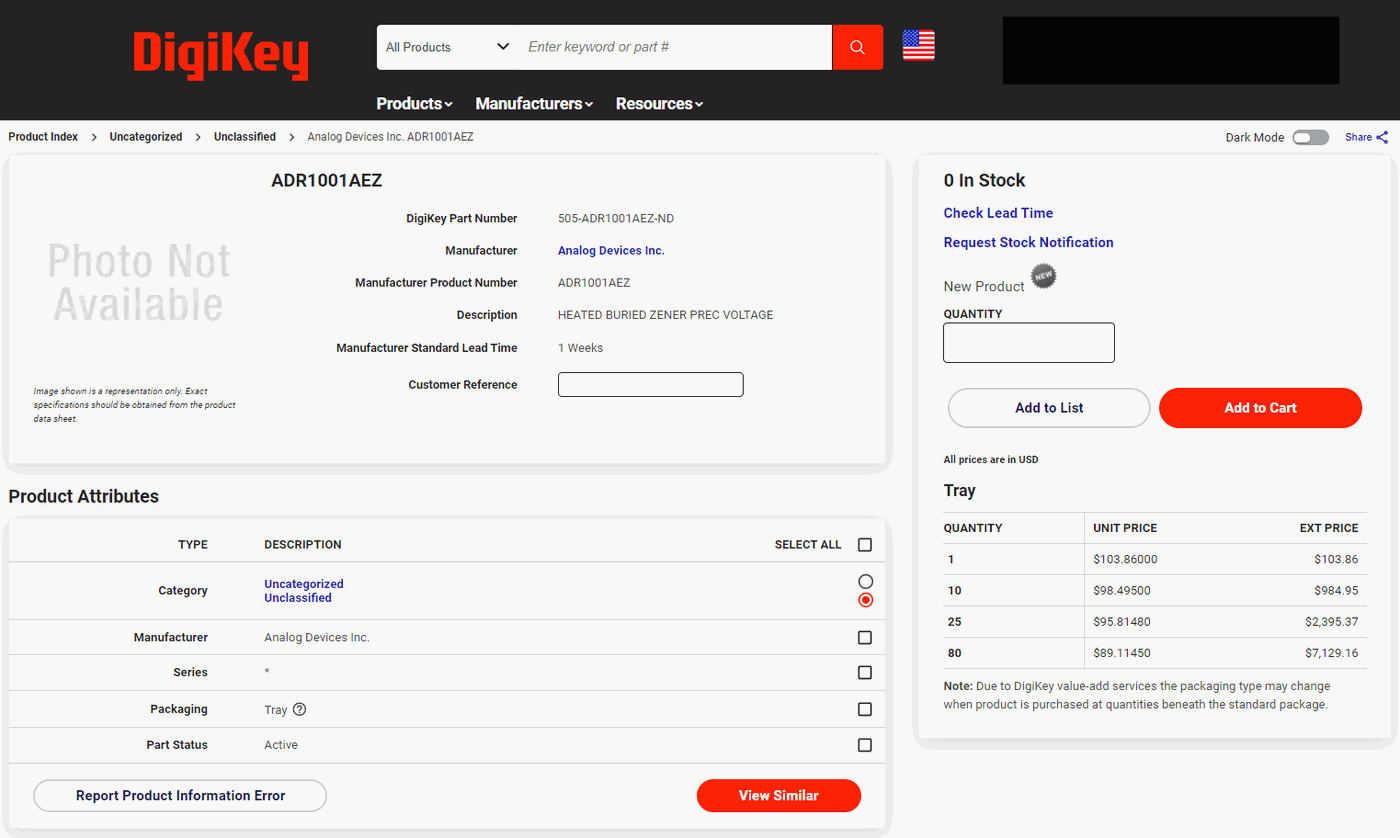
This 2024 project codenamed EX based on just released new Analog Devices ADR1001EZ chip. Similar to ADR1000AEZ it features newly redesigned buried zener core, this time with integrated resistors and amplifiers to provide ready to use scaled and buffered +5 V (or +10 V with) as well as raw +6.6 V from zener. Now that this new chip is finally almost available to the market by Analog Devices distributors, we can start a project to play with it in more details. ADR1001AEZ chip was added to Digikey store 19 March, 2024.
From the pricing point of view it looks pretty good, considering the fact that engineers don’t need long-lead time precision resistors like ADR1000 or LTZ1000 solution would need. Idea behind this EX project is to develop a flexible and easy to integrate precision and low-noise DC voltage reference module, without significant compromises on performance or functionality. It’s the evolution of knowledge gained from previous xDevs.com’s experiments, outlined in the publications below:
- Project KX – LTZ1000/LTZ1000A based DC reference with unbuffered 7V output, from 2015
- Project MX – LTZ1000/LTZ1000A based DC reference with unbuffered 7V output, from 2017
- Project FX – LTZ1000A based DC reference with bipolar 20mA 10V output stage, from 2017
- Project QVR-L – Quad LTZ1000/LTZ1000A based low-noise DC reference with averaging, from 2019
- Project QVR-A – Quad ADR1000 based very low-noise DC reference with averaging, from 2022
QVR project was quite expensive but very interesting practical test platform for lowering voltage noise of zener-based solution. It is also currently the main platform to test long-term drift of the ADR1000 chips, thanks to easy access to each zener voltage output and individual circuitry for each ADR/LTZ IC. Lot of details and measurements data is public in this repository. ADR1000 voltage output stability over 420 days, noise in 0.1 Hz to 10 Hz bandwidth, dependency of zener current to noise, temperature coefficient and multi-zener averaging effectiveness were evaluated.
Disclaimer
Redistribution and use of this article, any part of it or any images or files referenced in it, in source and binary forms, with or without modification, are permitted provided that the following conditions are met:
- Redistributions of article must retain the above copyright notice, this list of conditions, link to this page (https://xdevs.com/article/ref_ex/) and the following disclaimer.
- Redistributions of files in binary form must reproduce the above copyright notice, this list of conditions, link to this page (https://xdevs.com/article/ref_ex/), and the following disclaimer in the documentation and/or other materials provided with the distribution, for example Readme file.
All information posted here is hosted just for education purposes and provided AS IS. In no event shall the author, xDevs.com site, Analog Devices or any other 3rd party be liable for any special, direct, indirect, or consequential damages or any damages whatsoever resulting from loss of use, data or profits, whether in an action of contract, negligence or other tortuous action, arising out of or in connection with the use or performance of information published here.
If you are willing to contribute or add your experience regarding instrument repairs or provide extra information, you can do so following these simple instructions.
Certain commercial equipment, instruments, or materials are identified in this article to foster better understanding. Such identification does not imply recommendation or endorsement by the author or/and xDevs.com, nor does it imply that the materials or equipment identified are necessarily the best available for the purpose. Devices and components were not screened or conditioned prior to use in the electronic assembly, unless explicitly stated otherwise.
Design
This time around, module design would be focused on additional shielding and compact size to help with future integration of ADR1001-based module into various instrumentation and ADC/DAC projects. Unlike the traditional ADR1000/LTZ1000/LM399/ADR1399 zener references, we don’t need very expensive external high-stability resistors to generate stable and low noise +5V and -5V voltages. This makes ADR1001 perfect for integration at lower cost point once the chip hits the market availability.
This is an experimental project and may be revised and redesigned at a later time. It will contain additional test circuits and debug hooks to facilitate reconfiguration and performance study needs. It may not be the best way to make a user-friendly and easy to use device, so proceed with this knowledge in mind. Additional circuits and layout choices may also cause performance degradation compared to optimized design.
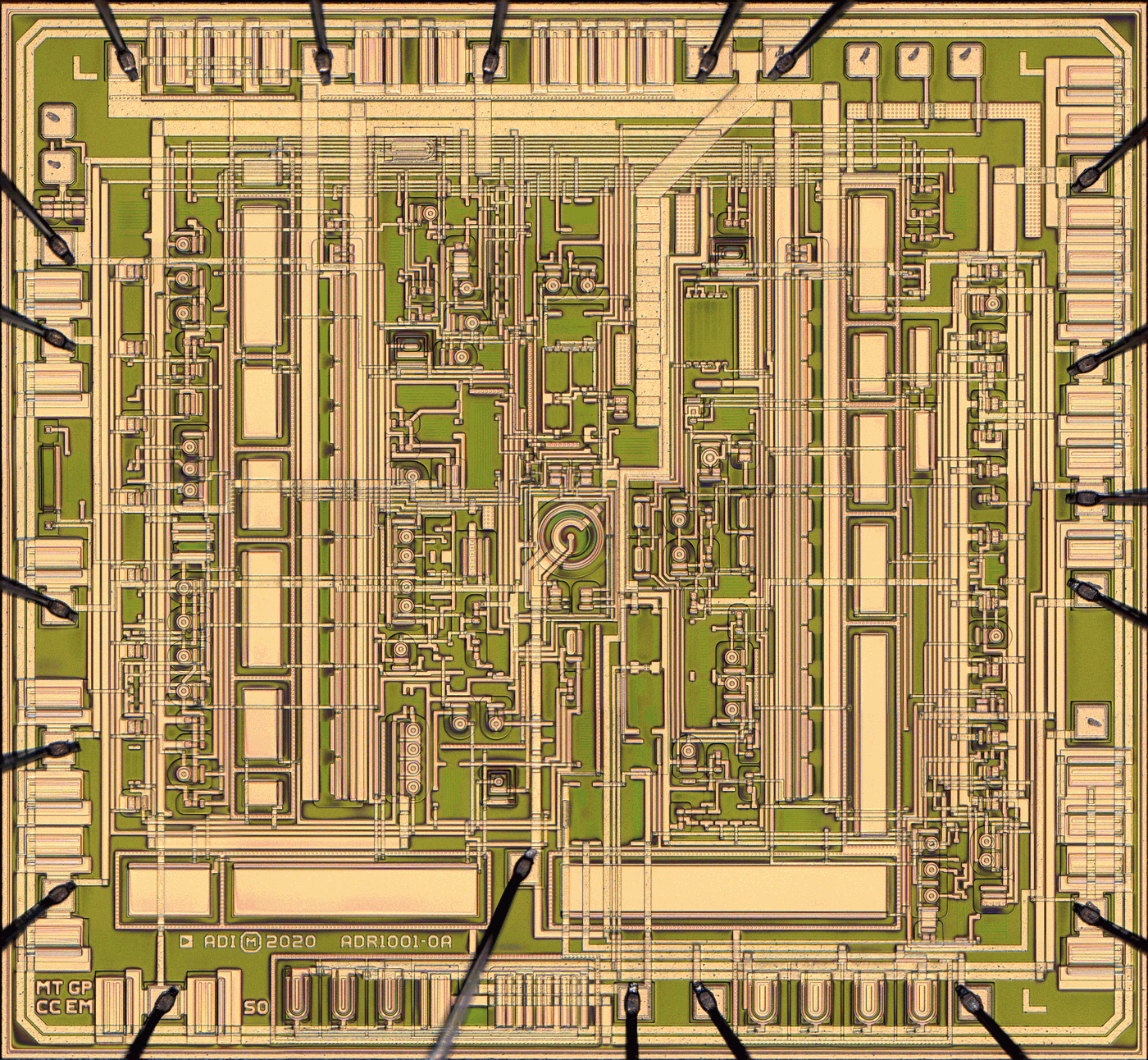
Richi’s Lab torn apart one of the ADR1001EZ chips here, so we don’t have to. Here we can enjoy their beautiful photograph. Be sure to check Richi’s site for many more.
Schematics for the prototype EX, Feb.29.2024
ADR1001 Datasheet, Rev.0 from Jan/2024
Analog Devices has own EVAL-ADR1001 module with USB Type C power supply based around switch-mode LTM8048Y integrated regulator and LT3045 post-regulation LDO. EVAL board is configured with single +5 V output provided at pair of banana sockets and SMA edge-launch connector.
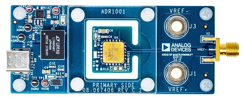
But this module does not provide easy ways to access various configuration or signals that ADR1001 expose for tinkering and more in-depth performance study. Hence, the decision to make own development module with more flexibility and capabilities.
Buried zener core and voltage control amplifier
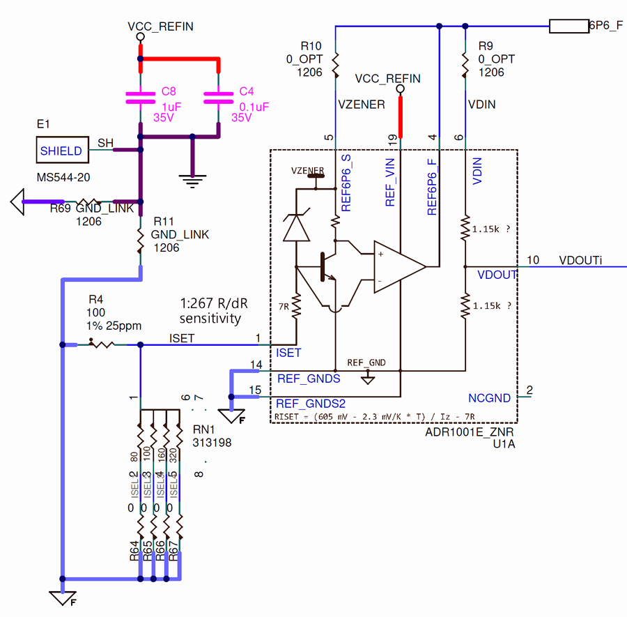
Output buffer stage amplifier with scaling resistors. Scaling resistors allow setting +5V, +2.5V or +10V outputs with just change of wiring. This output amplifier stage can be bypassed as well, as input connections from zener core domain is done externally by user.
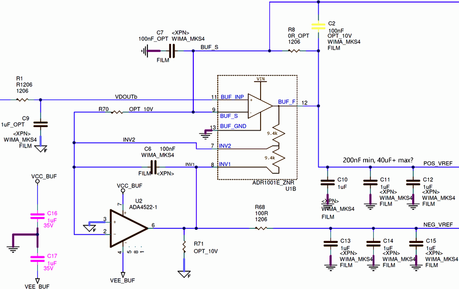
Heater and temperature control loop. This block contains all the circuitry for oven operation and power good open collector output for faults condition indication.
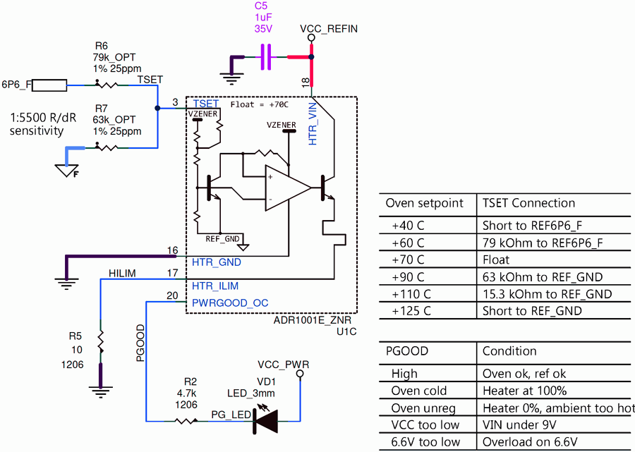
Schematics mostly replicates datasheet recommended circuit with additional jumper link and resistor positions to allow debug and verification to various aspects of the new chip operation.
To help with testing some additional digital sensors were also implemented into design. Temperature sensor U3 footprint for the high precision ±0.08 °C Texas Instruments TMP119 in tiny BGA case is placed next to ADR and ISET resistor area and temperature/humidity sensor Sensirion SHT45 placed near the LDO LT3045 regulator. Both sensors are interfaced with low-speed I2C digital bus and powered with separate fully isolated supply and ground pins. In noise sensitive design these parts can be left unpopulated.
PCB layout
Module dimensions are 60 × 25.4 mm with option to implement full shielding with Masach Tech MS544-20 steel tin-plated can. Reference can be reconfigured to provide single +5 V, unbuffered +6.6V zener, bipolar ±5 V or +10 V outputs. Zener current can be configured to multiple various levels, with a help of BMF resistor network. Onboard digital sensors are provided for temperature and humidity measurements, as well as EEPROM for the tracking of the data for each PCBA.
Rendering and configuration options
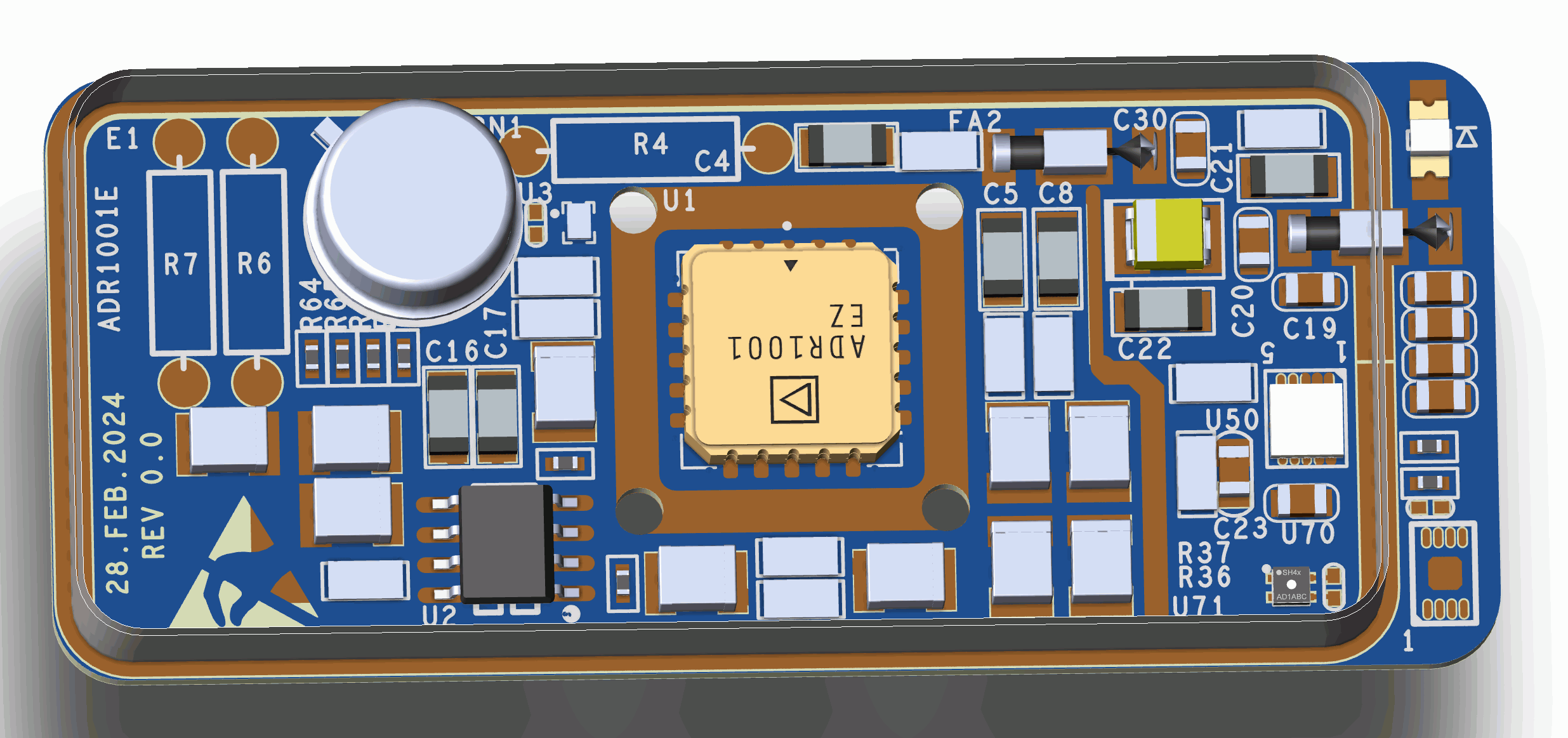
Nearly all the components are surface mount type to minimize the board area and simplify routing. Large precision resistors like R4, R6, R7 have large SMT pads for them without drill holes to clear interference with bottom-placed SMT connector J2.
Board is quite compact and does not have any significant heat sources, hence there is no special voodoo-looking cutout slots that volt-nuts love so much. Area around ADR1001 chip has keep out zone without any components and four 2.0 mm mount holes to provide 3D-printed plastic cap attachment in case such need occurs.
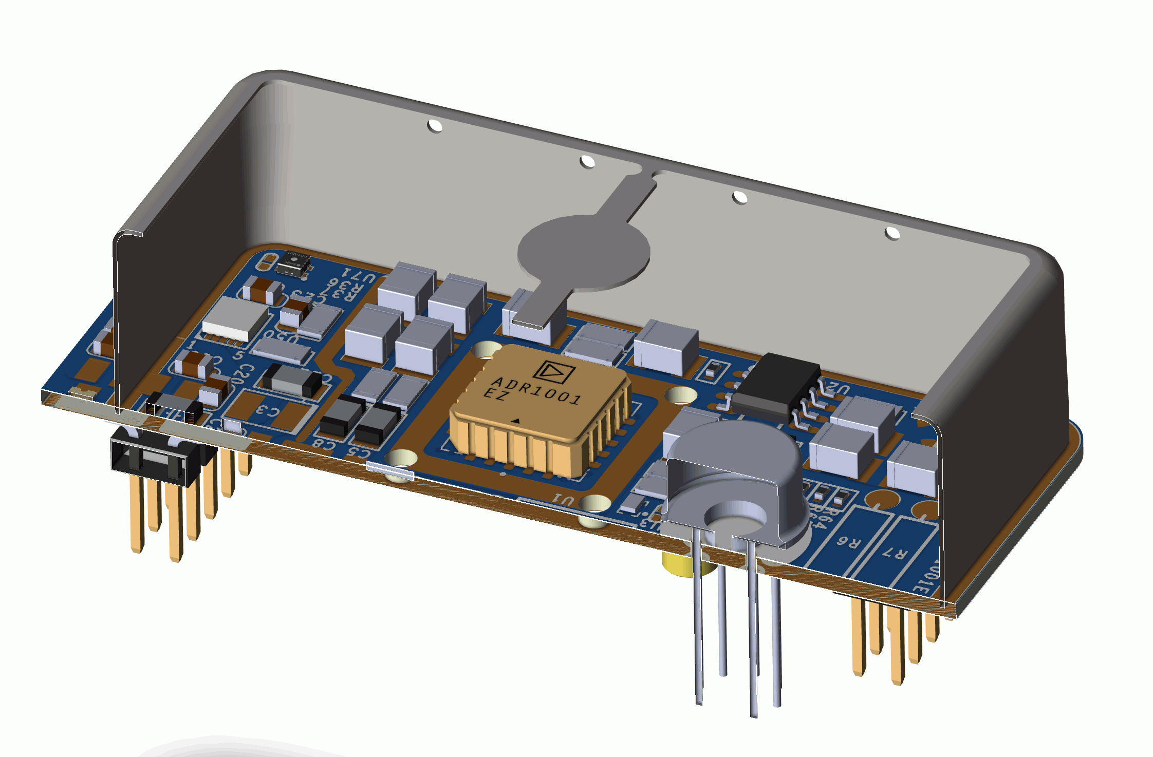
For clarity rendering show windowed steel shield can, but in practical builds shield can be fully sealed and enclosed. This will better protect internal DC reference from high frequency interference and noise coupling. Additionally, metal can shield prevents external airflow that can cause small thermally induced changes visible as very low frequency noise at the voltage output.
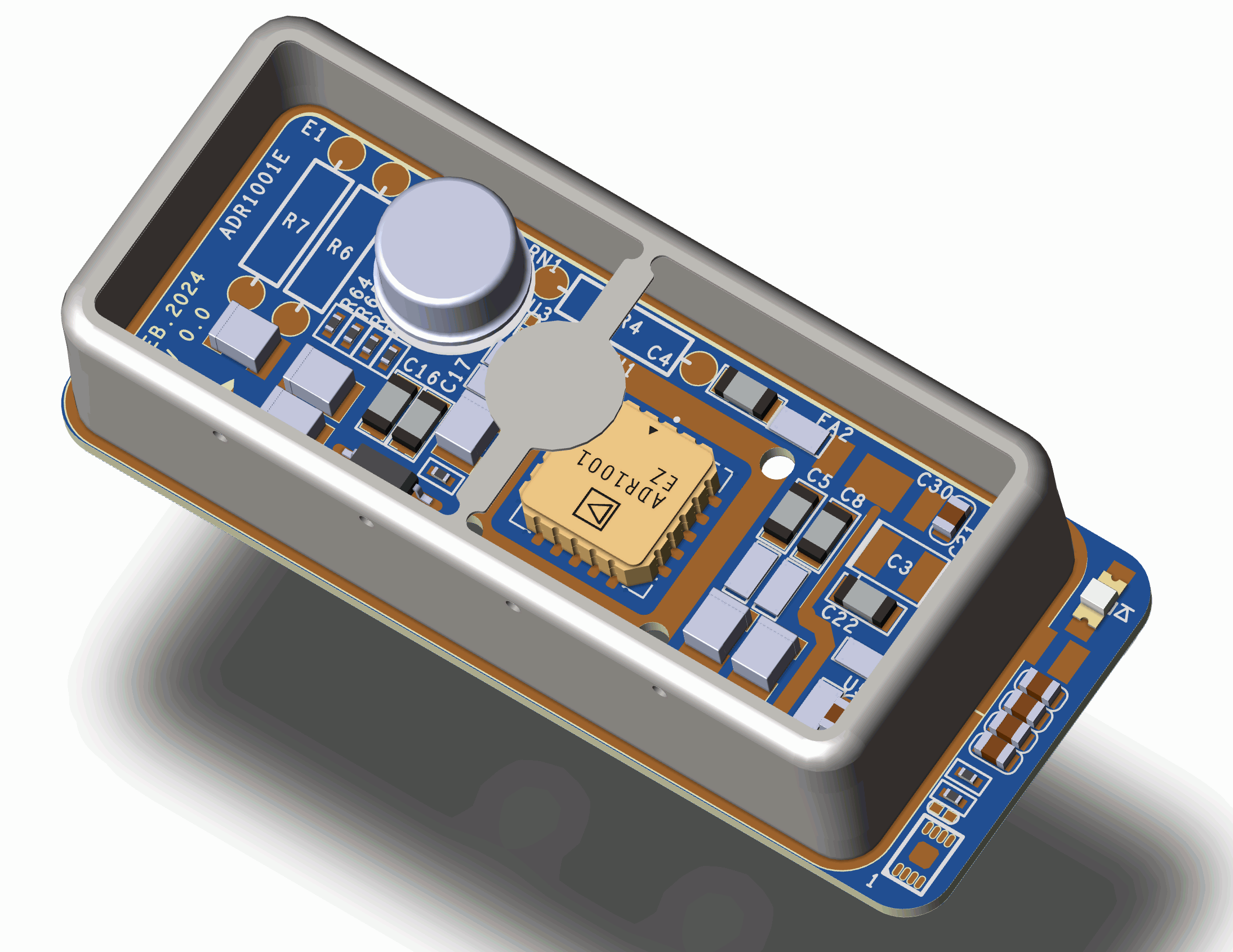
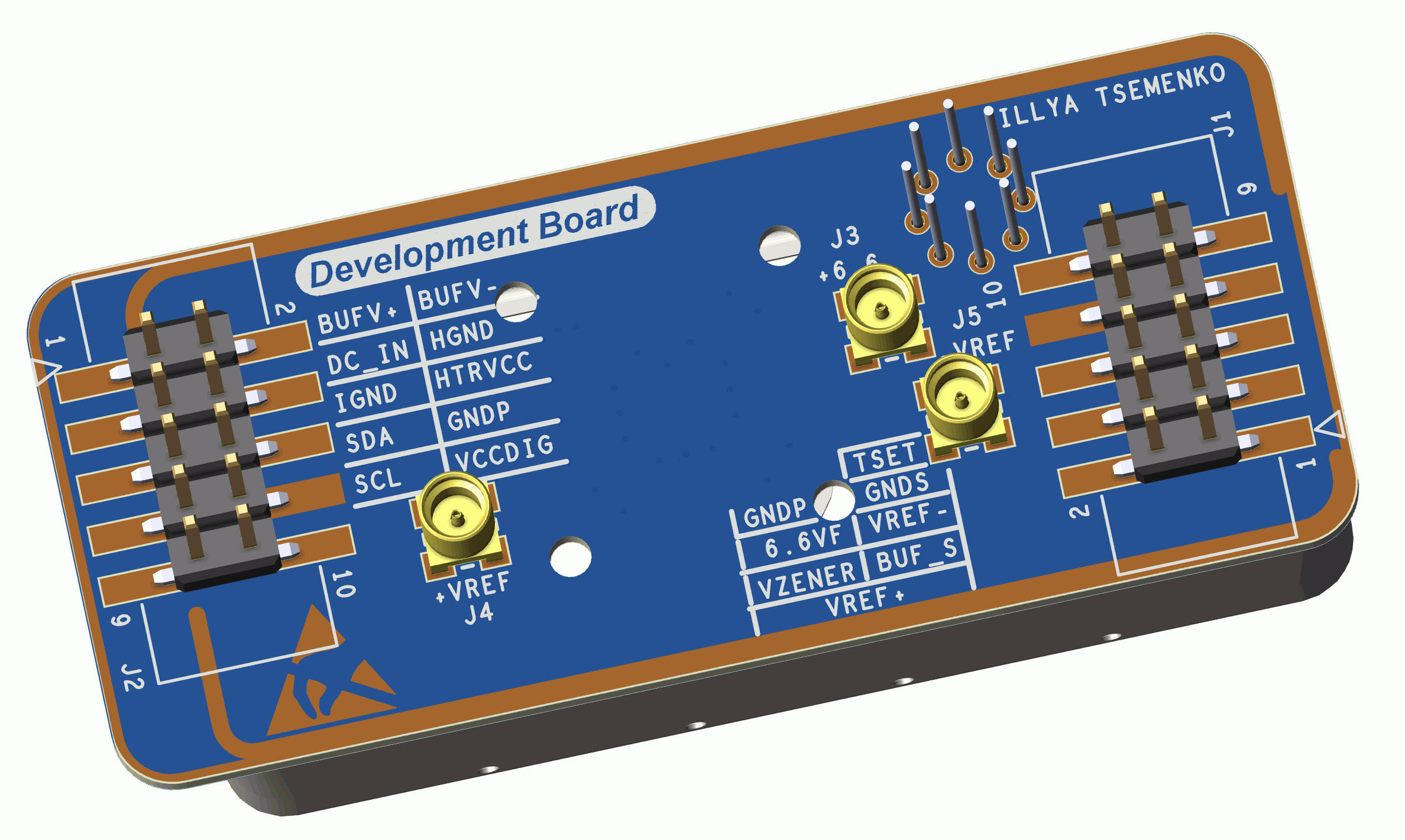
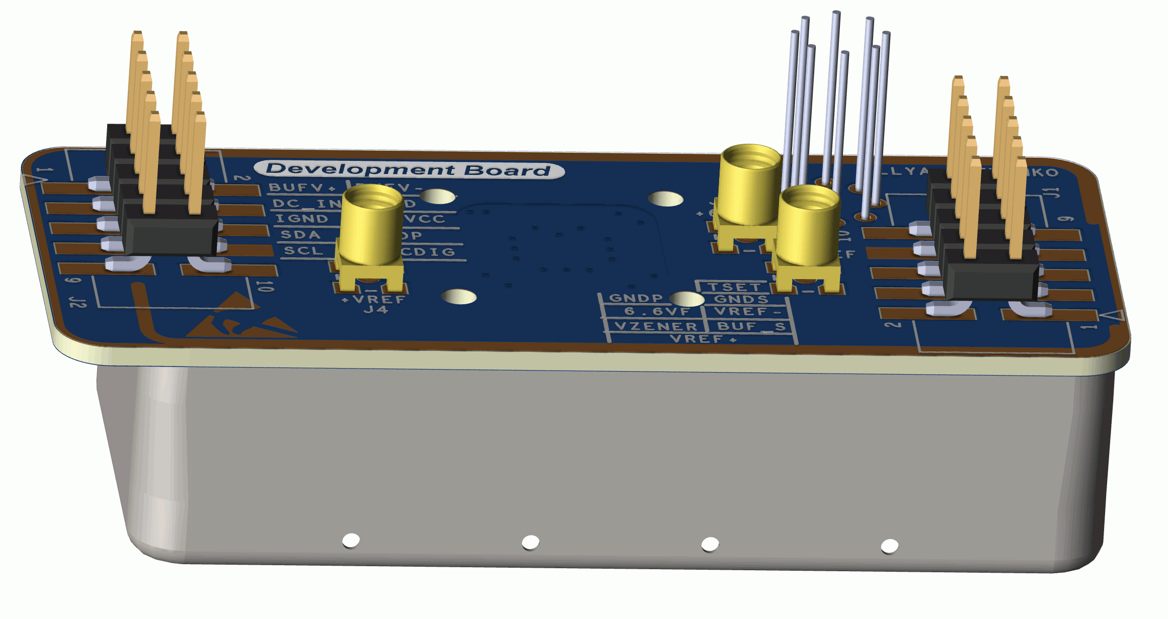
Interfacing to the carrier board or input/output signal cables is done via standard 2.54 mm pitch male pin-headers (either shrouded or unshrouded like on renders). If thermal EMF due to standard pin headers become a problem pads are large enough to have direct copper to copper wire connection with low-EMF solder alloy.
Small SMT-mounted MMCX coaxial ports are also available for the noise measurements at voltage outputs as well. In the final application these connectors can be left unpopulated.
In theory this board can be sealed quite well, perhaps even oil-filled with silicone or mineral oil. This would be one of the interesting experiments to be tested later on. Oil is much better thermal conductor than still air so oven inside of the zener chip would be working harder to maintain stability. And not sure how well PCB submerged in oil will behave for a long-term period. Oil will also break down eventually leaving a lot of mess, so it would make sense to use only if there is clearly measurable benefits, like reduced noise or thermal/humidity coefficients.
Component choice and bill of materials (BOM)
Resistor network RN1 and selection jumpers associated with it allow number of possible zener current levels to choose. Higher current results in smaller voltage noise at the zener core at expense of higher current consumption and possible drift rate acceleration. Some typical configurations are summarized in the table.
| Populated resistors links | ISET resistance | Zener current | ||
|---|---|---|---|---|
| with RN1 or R4 | calculated value | +125 °C | +70 °C | +40 °C |
| R66 | 159.1 Ω | 1.91 mA | 2.63 mA | 3.09 mA |
| R67 | 319.1 Ω | 0.97 mA | 1.34 mA | 1.57 mA |
| R66 + R67 | 106.17 Ω | 2.81 mA | 3.85 mA | 4.53 mA |
| R65 | 99.1 Ω | 2.99 mA | 4.11 mA | 4.84 mA |
| R64 | 79.1 Ω | 3.69 mA | 5.06 mA | 5.96 mA |
| R62 + R67 | 63.39 Ω | 4.51 mA | 6.19 mA | 7.29 mA |
| R65 + R66 | 61.06 Ω | 4.67 mA | 6.41 mA | 7.54 mA |
| R64 + R66 | 52.83 Ω | 5.31 mA | 7.29 mA | 8.57 mA |
| R65 + R66 + R67 | 51.26 Ω | 5.45 mA | 7.48 mA | 8.81 mA |
| R64 + R65 | 43.99 Ω | 6.23 mA | 8.55 mA | 10.06 mA |
| R64 + R65 + R66 | 34.46 Ω | 7.66 mA | 10.52 mA | 12.37 mA |
| R64 + R65 + R66 + R67 | 31.1 Ω | 8.33 mA | 11.44 mA | 13.46 mA |
| None, R4 fixed resistor used | 200 Ω | 1.53 mA | 2.11 mA | 2.48 mA |
| None, R4 fixed resistor used | 120 Ω | 2.50 mA | 3.44 mA | 4.04 mA |
| None, R4 fixed resistor used | 100 Ω | 2.97 mA | 4.07 mA | 4.79 mA |
| None, R4 fixed resistor used | 80 Ω | 3.65 mA | 5.01 mA | 5.90 mA |
| None, R4 fixed resistor used | 50 Ω | 5.57 mA | 7.65 mA | 9.00 mA |
Fixed position R4 resistor also provided for cheaper implementation without the custom VPG BMF resistor network RN1, in case this design replicated by our readers. Per datasheet page 18 sensitivity ratio to performance of this ISET resistor is 1/267. Because of this in practical example ISET resistor shift of 100 µΩ/Ω would result in 0.374 µV/V shift in the output of +6.6 V zener voltage. This figure also hints us the requirement for ISET resistor stability to be better than 13.4 µΩ/Ω/year if we want to keep ISET resistor contribution to annual stability below 0.05 µV/V. Most of BMF hermetic resistors specified and capable of much smaller drift, especially with very low dissipated power like in this application.
There is a typo in the datasheet calculation example with extra zero in result. This test will be easy to do once the module is assembled by adding known large value parallel resistor across ISET resistor and measuring output value change.
Test chips
| IC device | Datecode | Process | Notes |
|---|---|---|---|
| ADR1001AEZ | 2407 | Bare IC bake +120 °C from 6/18/2024 until 6/26/2024, and +140 °C until 7/5/2024 | N/A |
| ADR1000AHZ | 22xx | Bare IC bake +120 °C from 6/18/2024 until 6/26/2024, and +140 °C until 7/5/2024 | N/A |
| ADR1000AHZ | 22xx | Bare IC bake +120 °C from 6/18/2024 until 6/26/2024, and +140 °C until 7/5/2024 | N/A |
Assembly
TBD…
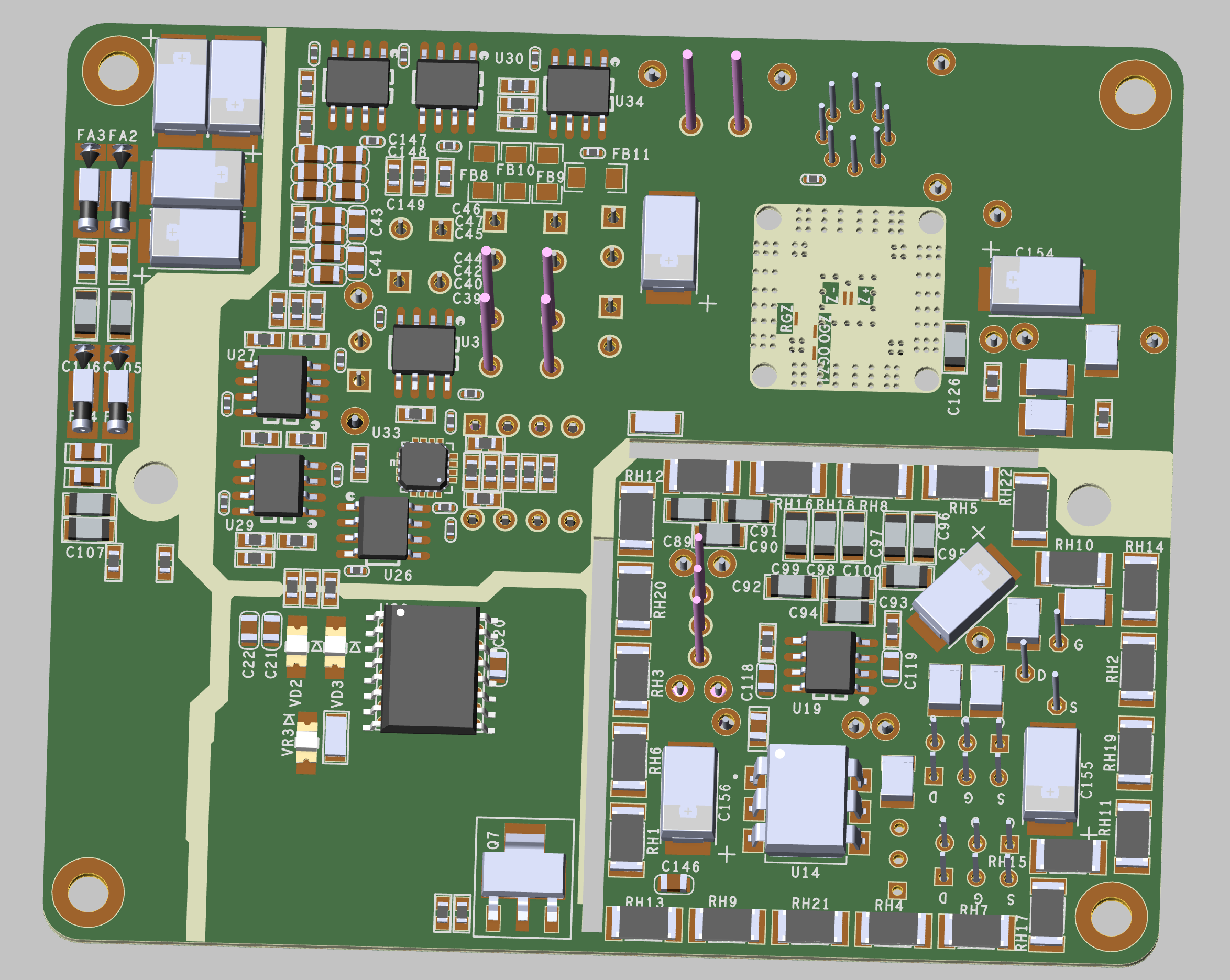
EX-LN version
There is also experimental module design concept with an active low noise output stage. I wanted to implement some additional control and monitoring circuits , so this module got larger footprint board, but still small enough to fit in enclosure of 732B charger for battery backed power operation. Enjoy the renders:
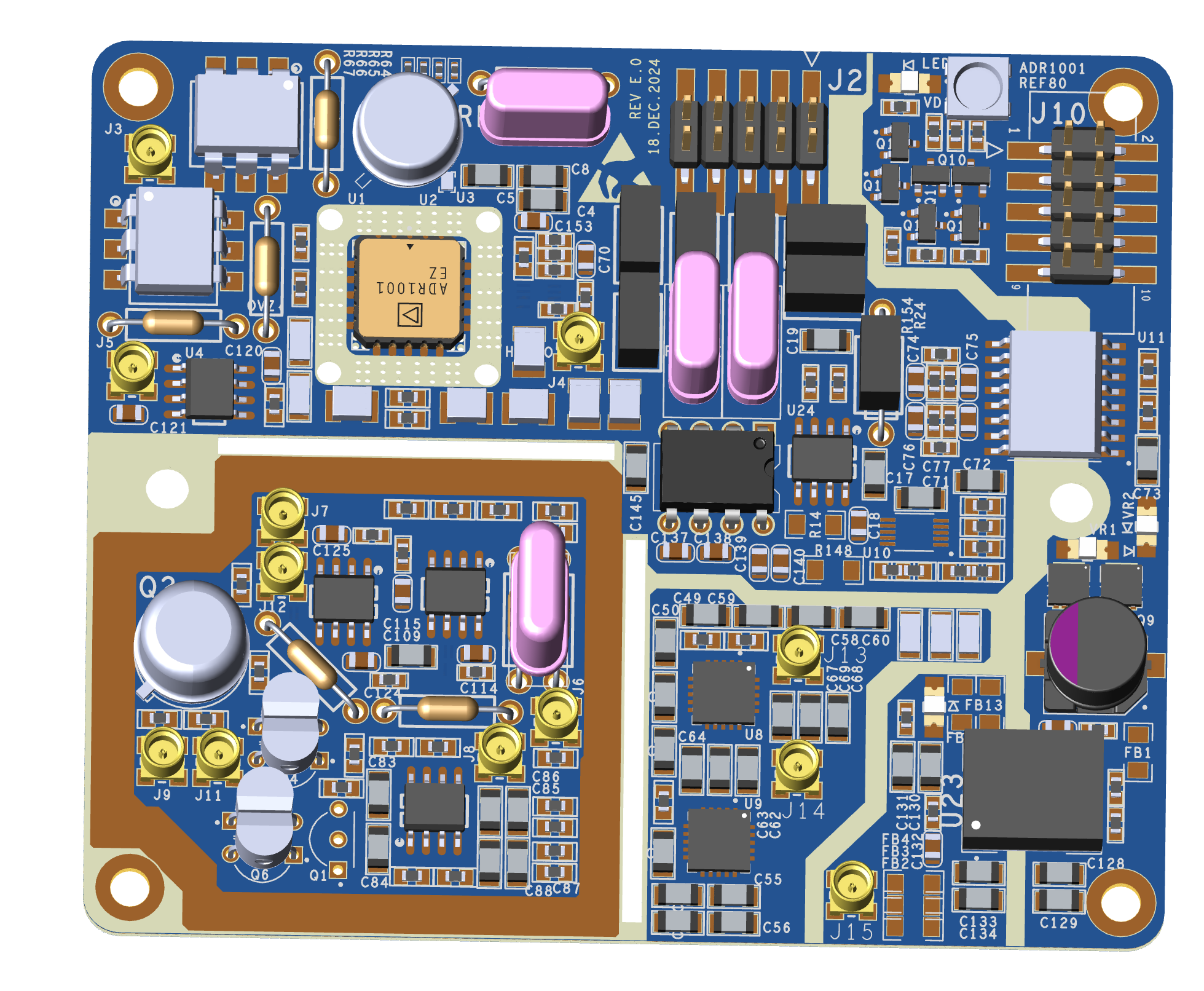
Back side is quite busy as well, because the output 6.6V / 10V stage have active heater ring with RH* resistors, plus full analog PID controller. This module now has hardware footprint compatible with ADR1001EZ or new Texas Instruments REF80 chips.
Key features:
- New output driver stage for 10V scaling
- Oven heater ring for output driver stage
- Oven analog controller option
- Oven PID analog controller option
- Onboard TMP119 temp sensor
- Onboard isolated high heater/high Iz current binary control for ADR1001 chip
- Isolated power option
- +11.5/-6V power option for 732B charger
- Fits 732B charger enclosure space
- New experimental active output filter
- Adjustable zener current for ADR1001
- Measurement test points with MMCX ports
- TI TPS7 positive/negative LDOs onboard
- Onboard RGB LED to indicate oven ready status (cold/good/hot)
- Digital heater power meter option (TI INA228)
Performance evaluation and testing
Planned benchmarks for EX reference will include:
- Long-term drift (stability) verification against stable commercial references
- Output retrace to previous value after power cycling
- Output noise in 0.1 Hz – 10 Hz bandwidth
- Temperature coefficient of both +6.6 V and scaled outputs
- Power supply rejection ratio of the voltage output
- Load regulation of the voltage output
- Total power consumption at few fixed operation points
- Recovery time after power cycling
- Recovery time after thermal cycling
- Gravity dependence to output voltage (orientation test)
- Pressure coefficient of the voltage output
TBD…
Conclusion
TBD…
Real-time discussion about this article and related stuff is very welcome at our own xDevs.com IRC-chat server: xdevs.com (standard port 6010, channel: #xDevs.com).
Projects like this are born from passion and a desire to share how things work. Education is the foundation of a healthy society - especially important in today's volatile world. xDevs began as a personal project notepad in Kherson, Ukraine back in 2008 and has grown with support of passionate readers just like you. There are no (and never will be) any ads, sponsors or shareholders behind xDevs.com, just a commitment to inspire and help learning. If you are in a position to help others like us, please consider supporting xDevs.com’s home-country Ukraine in its defense of freedom to speak, freedom to live in peace and freedom to choose their way. You can use official site to support Ukraine – United24 or Help99. Every cent counts.
Modified: Dec. 31, 2024, 6:03 p.m.