Contents
- Intro
- Disclaimer
- Manuals and documentation
- Project concept and workflow
- Fluke donor chassis. Special Hulk-edition
- Front panel repairs
- A22 – Fluke mains power transformer assembly
- A3,A4 – Mainboard backplanes
- A19 – In-guard Power Supply PSU PCBA
- A20 – Processor board
- A21 – Rear interface and expansion board
- Modularity and 5700A/5720A flexible diagnostics
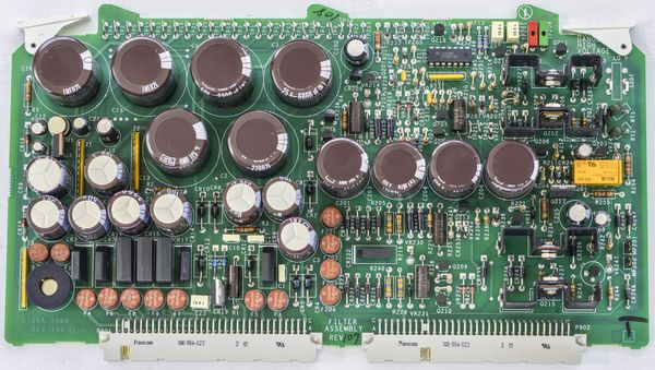
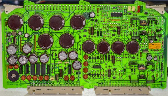
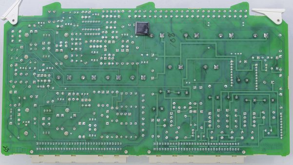
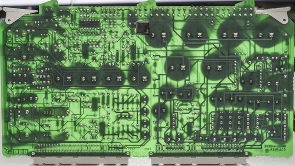
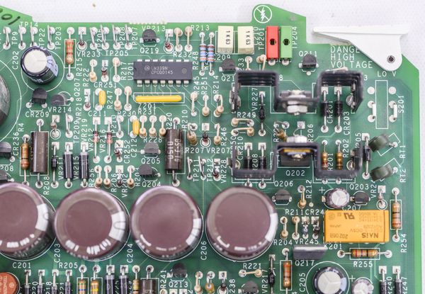
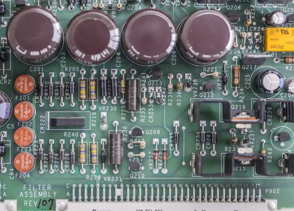
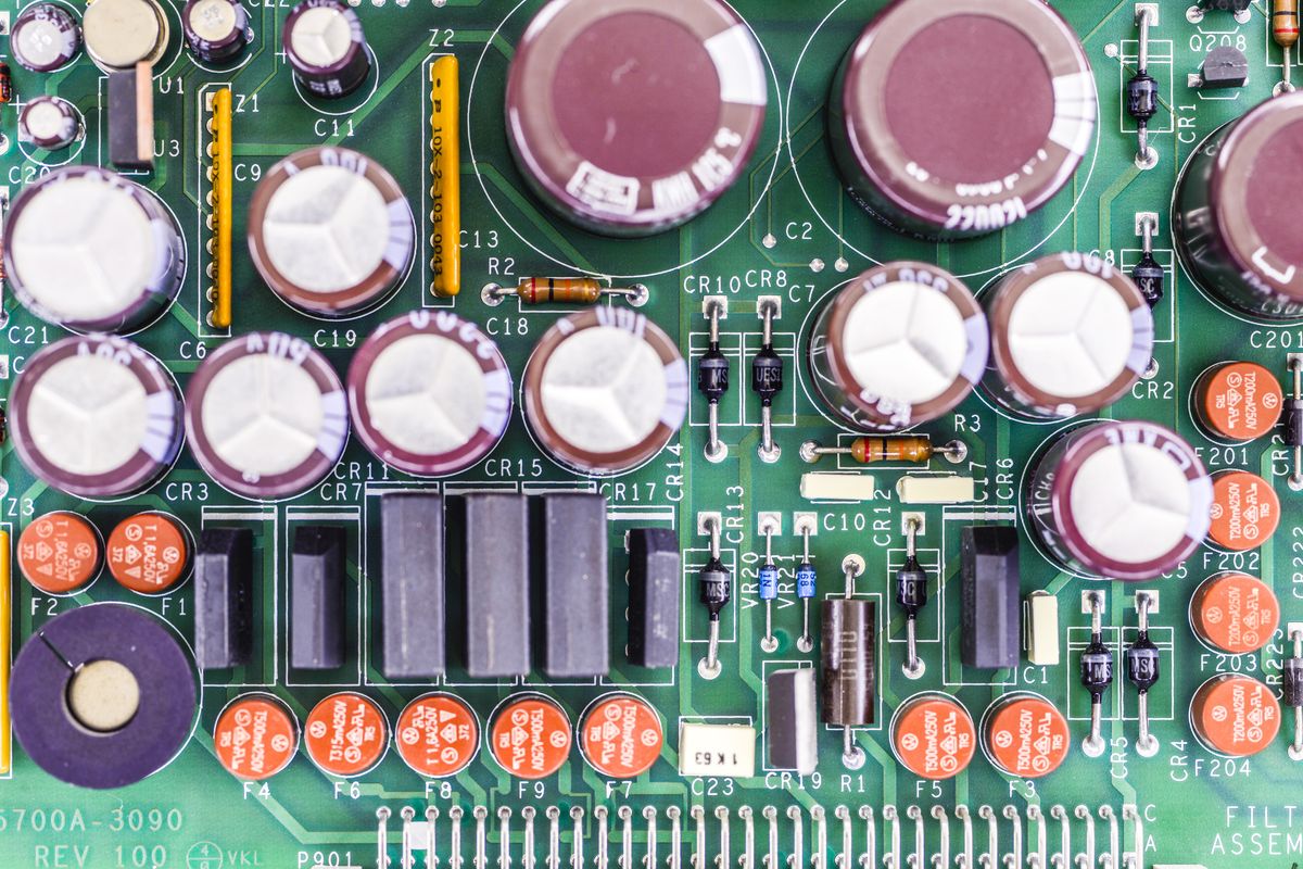
- A18 – Filter/PA PSU PCBA from Fluke 5700A MFC
- A18 – Filter/PA PSU PCBA from Fluke 5720A MFC
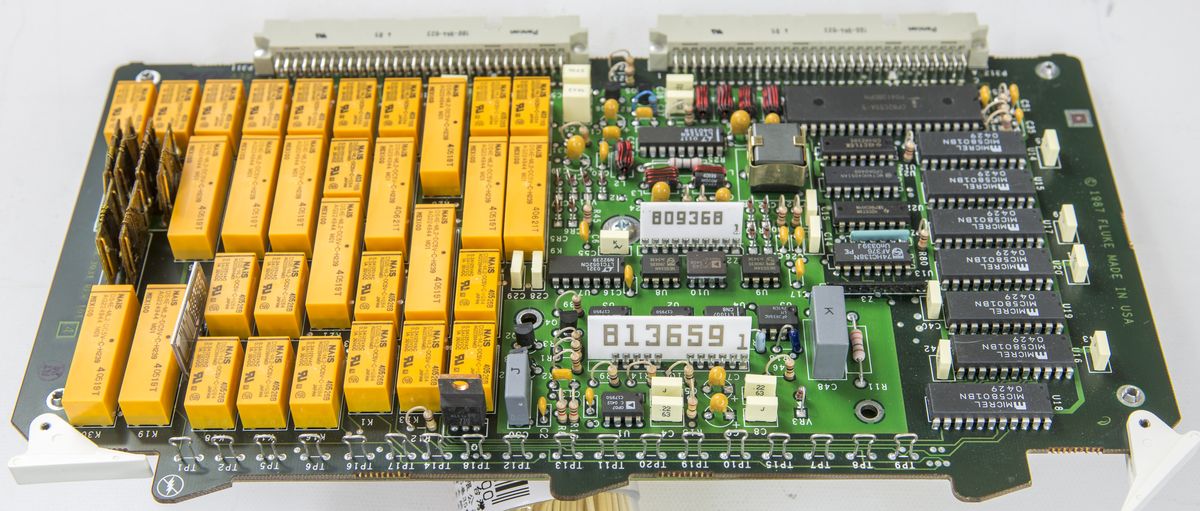
- A8 – Switch Matrix assembly
- A11 – DAC PCBA from Fluke 5700A MFC
- What is the Ref-Amp?
- A11 – DAC PCBA from Fluke 5700A II MFC
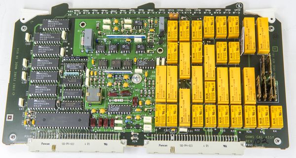
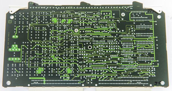
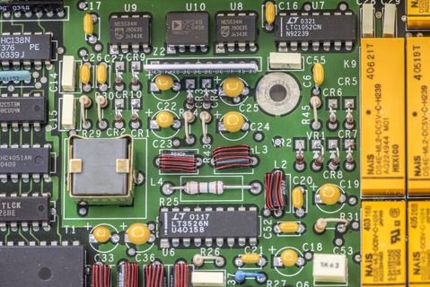
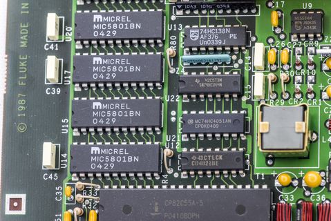
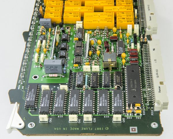
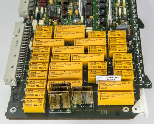
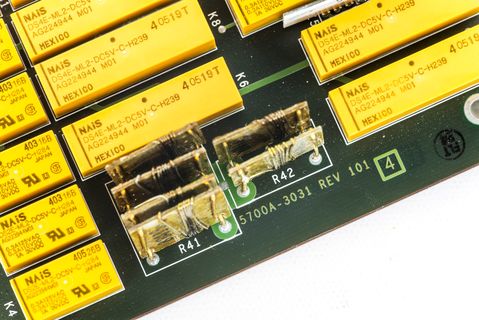
- A9 – Fluke 5720A Ohm Calibration board
- A10 – Ohms Main PCBA from Fluke 5700A MFC
- Intermediate functionality check
- A12 – Oscillator Control PCBA from Fluke 5700A MFC
- A16 – PA PCBA from Fluke 5700A MFC
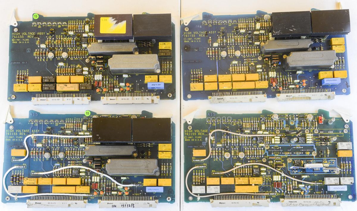
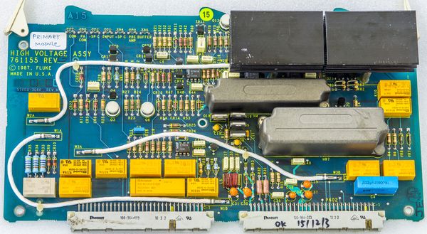
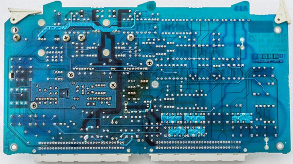
- A15 – High-voltage/High-current assembly
- Wideband option A5 – Output PCBA from Fluke 5700A MFC
- Wideband option A6 – AC Oscillator PCBA from Fluke 5700A MFC
- Extenders for repairs and testing
- Fluke 5725A ‘Booster’ amplifier for voltage/current ranges extension
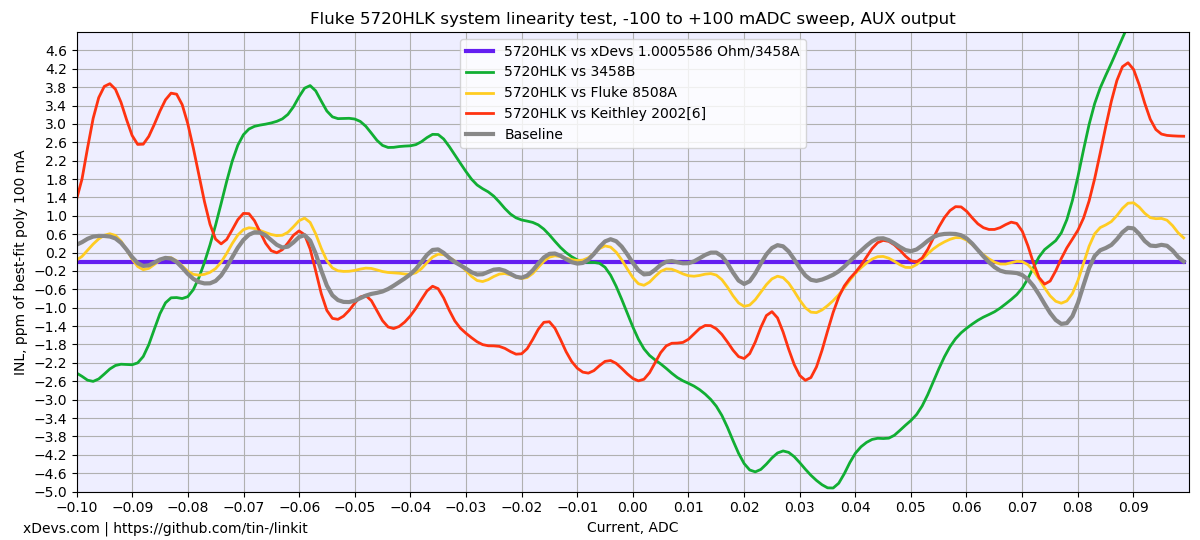
- Performance benchmarks
- Summary on spent resources
Intro
Well, not quite DIY calibrator, but actually a built from parts complete Fluke 5720A. Over few years we gambled and collected random used/broken Fluke parts and with extensive deep-dive in component level repairs and troubleshooting managed to get something useful.
Everything started with remote over-the-internet use and measurement experiments utilizing few Fluke 5700A/03 and Fluke 5700A multi-function calibrators. It was not far from there to fullfill our dream to have metrology-level Fluke MFC in permanent ownership. This would enable precision voltage and current experimentation over any duration of time and as a transfer source to calibrate various DUTs in lab. Such large investment also have practical outcome, as we have more than four 8½-digit DMMs with cost of complete calibration over $2000 USD, per each unit, logistics/insurance not included. With help Artifact Calibration in 5700A/5720A and use of fixed calibrated standards, we can also aim for shorter that annual cycle on DMM calibrations.
As result 57xxA series units are great transfer standard tool to use, with our already calibrated 10.00000V DC standards, like Wavetek 7000, Fluke 732B and 1 Ω / 10 KΩ FSL935 heated resistance standard and famous ESI SR104 10 KΩ. Artifact Calibration of 5700A allow transfers to great accuracy with other cardinal voltages/currents/resistances.
This project actually started few years ago, as a sweet dream of any hobby electrical metrologist. That is to have very own personal high-performance multi-function calibrator, like Fluke 5700A or 5720A. These instruments are work horses of any serious calibration laboratory, but very rare sight in personal man’s cave labs due to high cost. Current MSRP for 5720/5730A series even in vanilla option-less package is over $60000 USD. Once you add Wideband option for 30MHz output, custom Fluke low-thermal cable sets, transit case the price tag of the total solution will shoot up to over $70000 USD easily. And that is not considering the cost of the proper calibration even just for one year.
5700A Series II and later 5720A were 1994 year refresh of original calibrator design to improve reliability, noise performance on low mV ranges and overall stability. 5720A was in production for few decades before release of facelifted Fluke 5730A in 2016. In this article we will also search for major differences between the 5720A and 5730A from public information available.
How would a dedicated person make the dream to have high-performance calibrator at home to come true, without selling both arms, legs and eyes to nearest Fluke Calibration branch? What we say here today – go build our own calibrator from scrap parts!
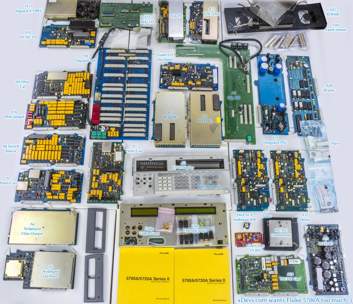
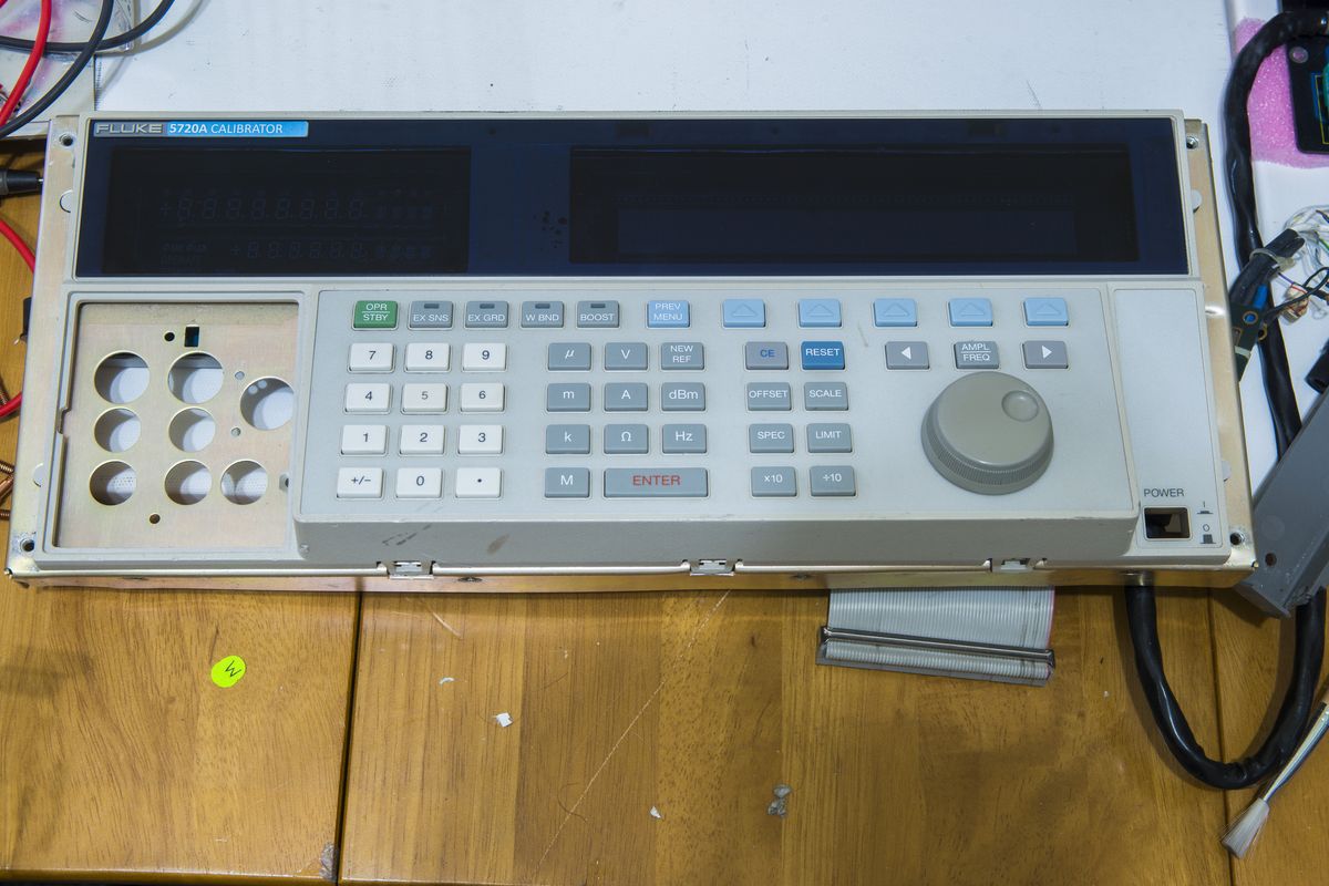
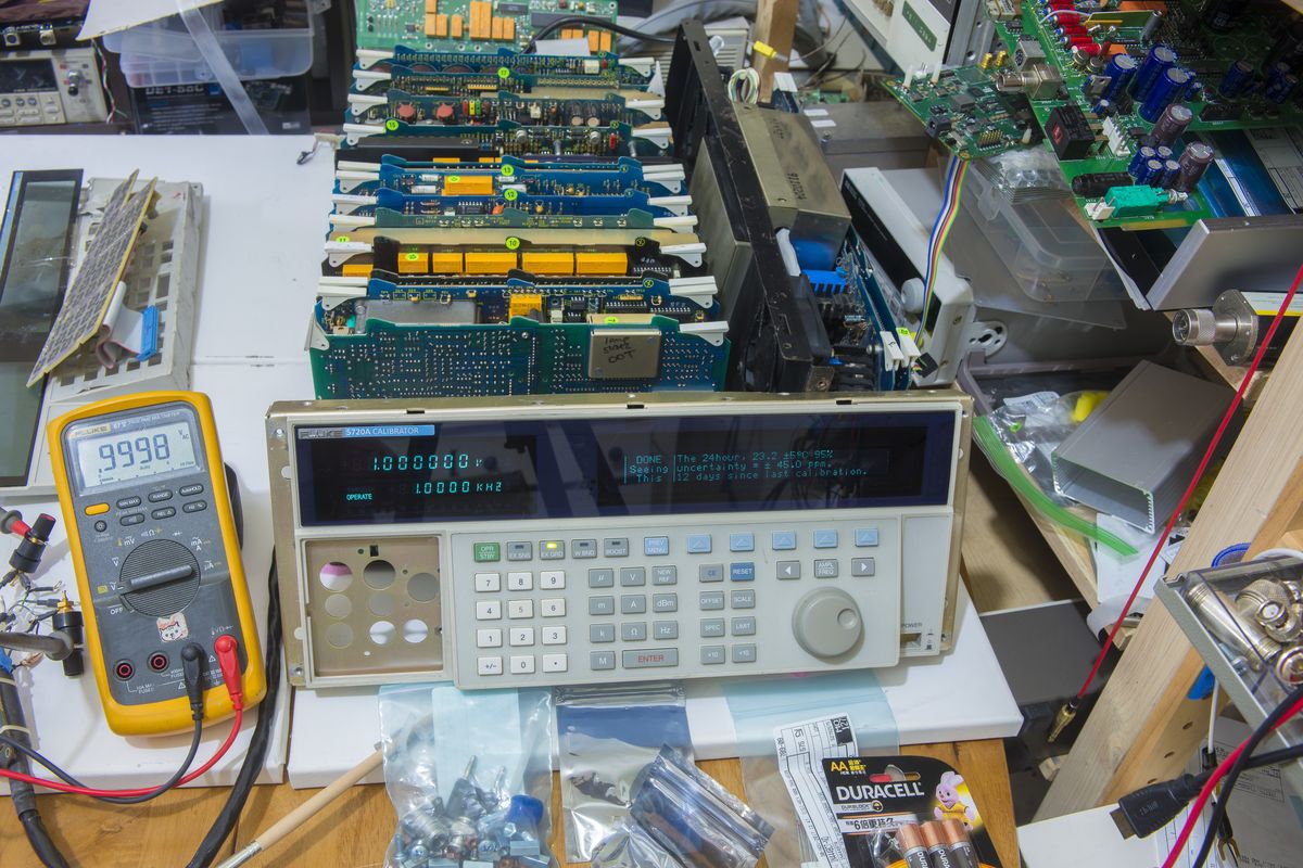
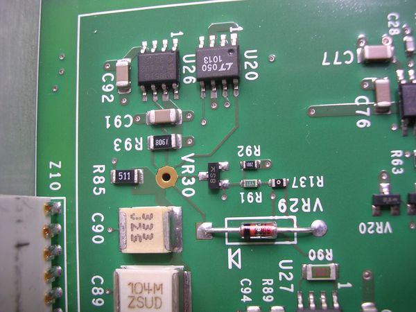
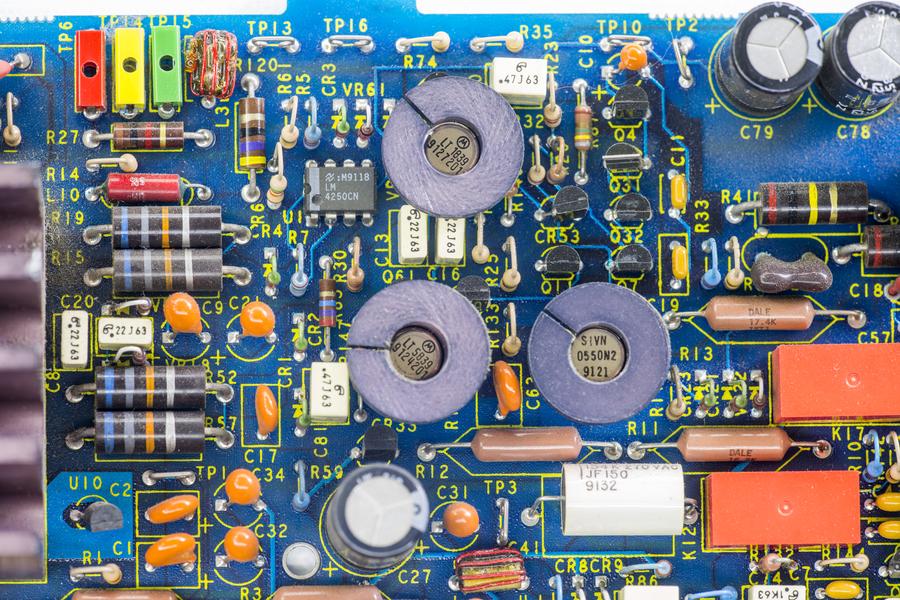
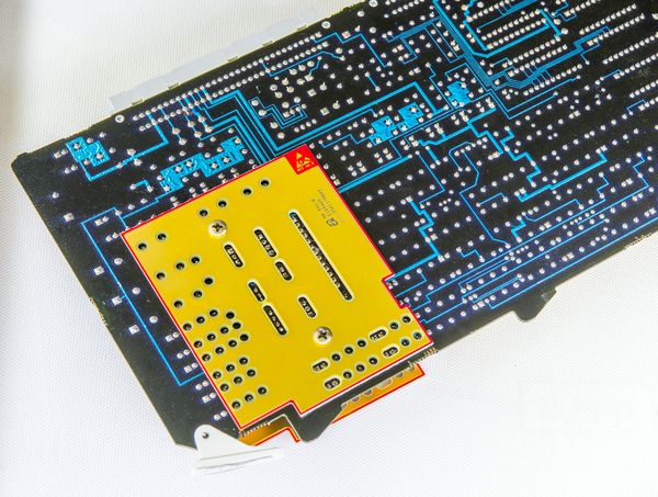
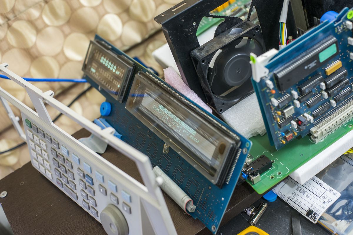
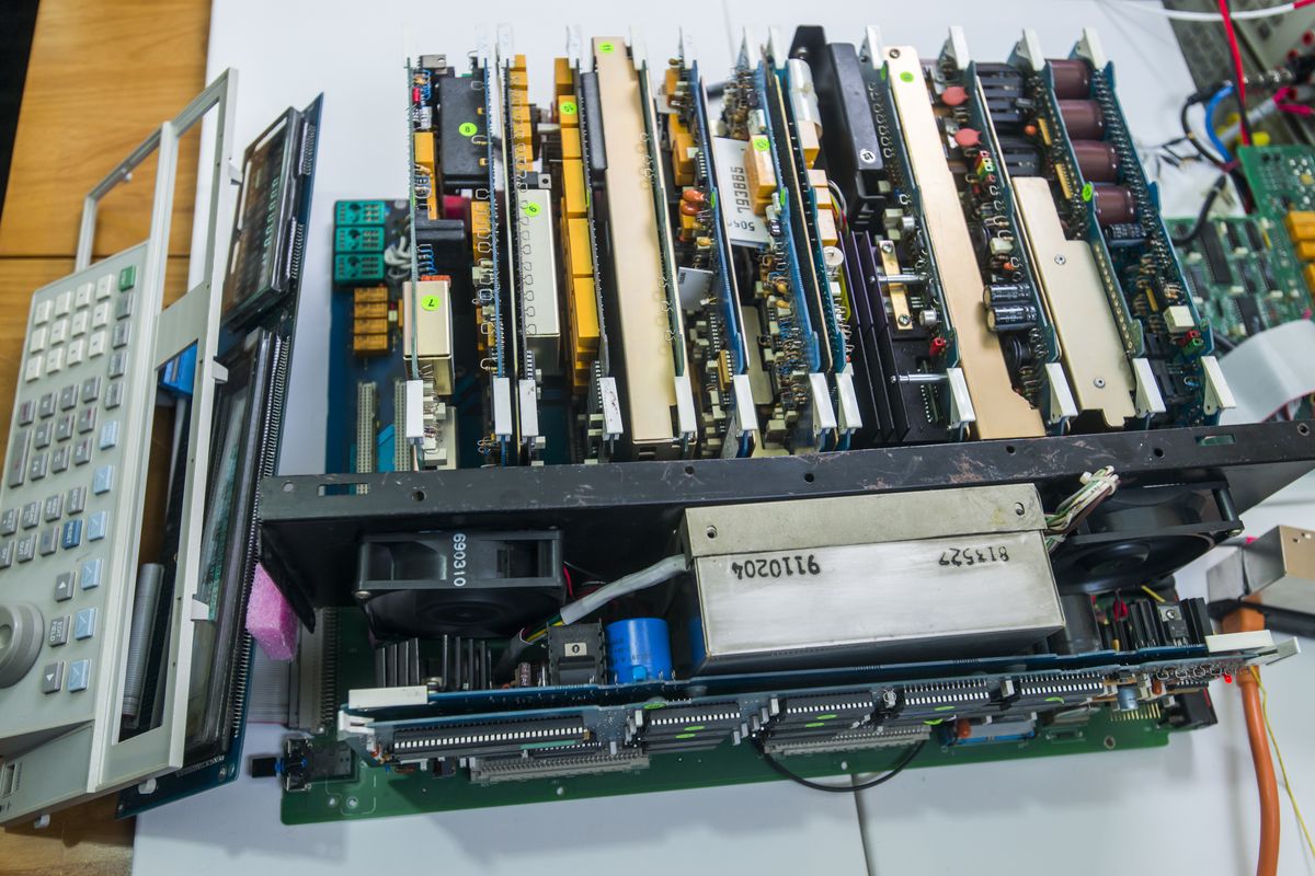
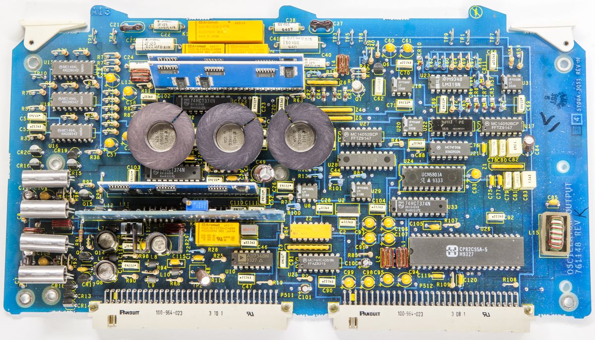
Image 1: Random bits and pieces, lego-version of the 57xx series calibrator hardware
It all started with getting heart core of the calibrator, single PCBA module – 5700A A11 REF/DAC assembly. This module is a paramount for unit’s performance, with precision ultra-stable heated DC reference, PWM DAC circuitry and null-meter ADC. Original idea was to reuse the reference as standalone device to compare voltage stability with my xDevs.com KX and xDevs.com FX LTZ1000-based DC references. But board need lots of power rails to even get oven working, so that project sat on shelf for months in “idea” state. Then we got yet another 5700A A10 Main Ohms PCBA populated with custom Fluke hermetical thin-film resistance networks from 10 Ω to 100 MΩ.
And at this point, it become obvious that there is no stopping at just two boards, and mission impossible to obtain full set. Some calibration labs do sell dead BER modules and scrap from shelves, so this fact was exploited behind the scenes over last few years.
Getting full puzzle piece set for this little project was pricey and lengthy process, but because it was spread over months, it didn’t felt as painful as buying used unknown condition 5700A off ebay for $10-25K they usually fetch. After all, xDevs.com did not want to miss fun from learning and troubleshooting each module/circuit? Learning electronics is different process for each engineer, and in this case xDevs.com way to learn about 7½-digit calibrator design is the hard one – buy random dead parts from random calibrators and try to make them all work together and give ppm-stable output that would meet Fluke specifications. Nothing wrong with that idea, what could go wrong, right?
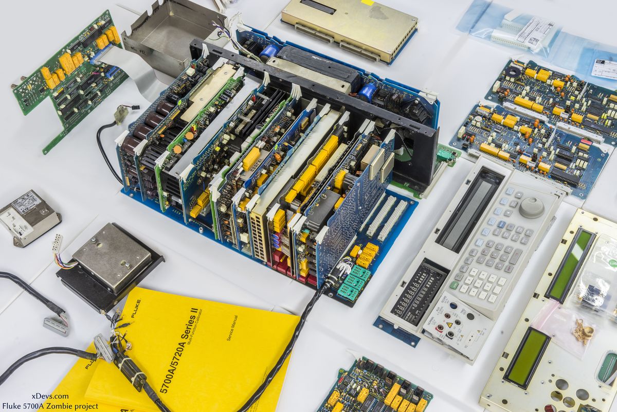
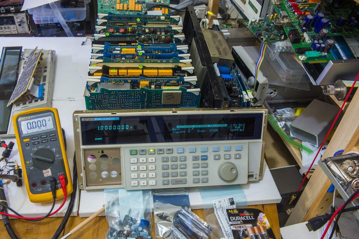
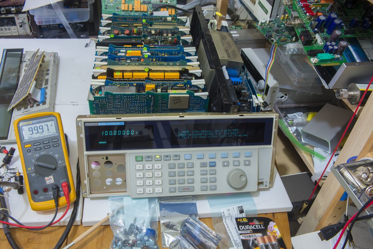
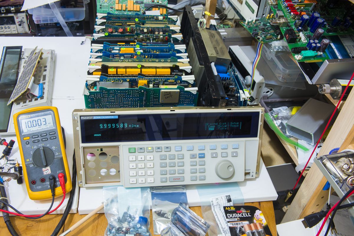
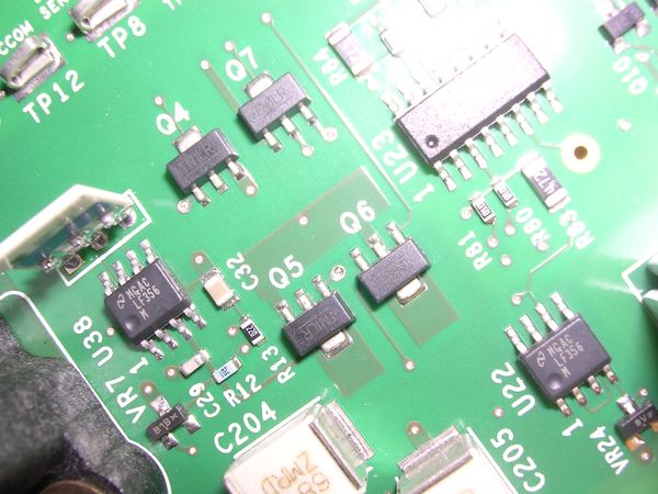
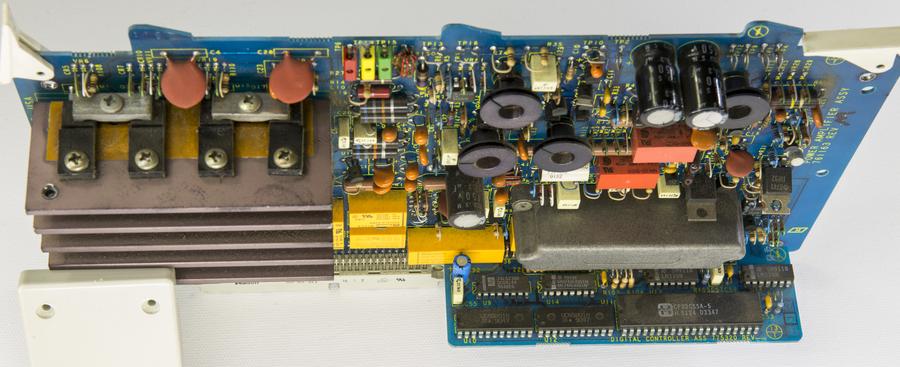
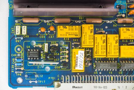
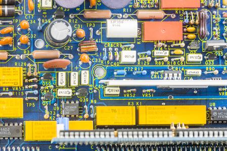
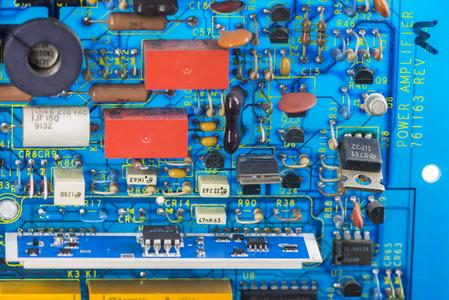
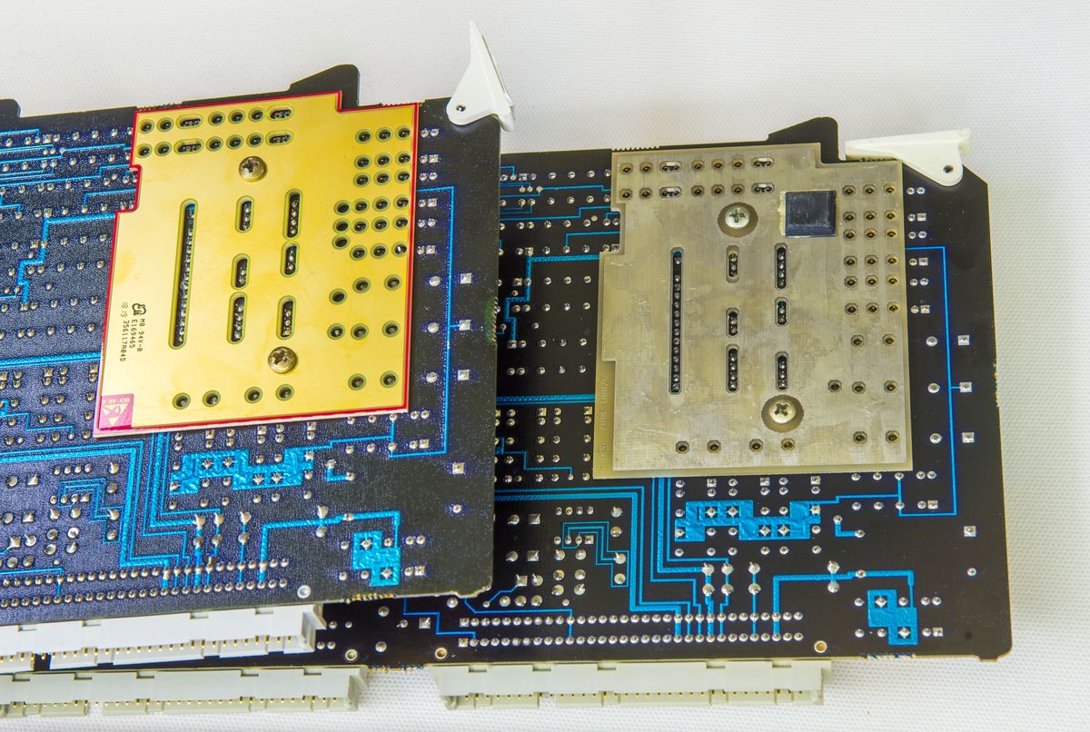
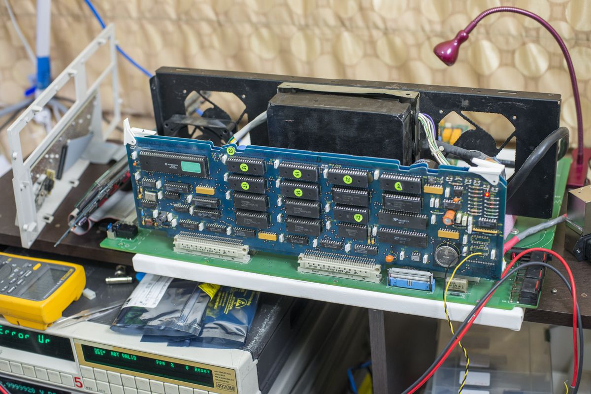
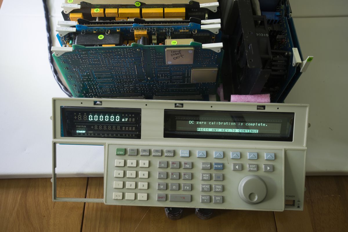
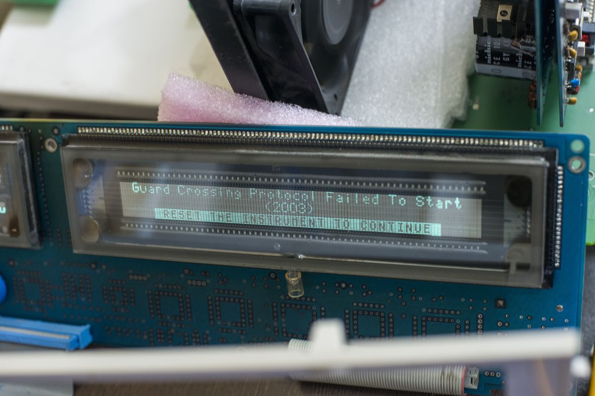
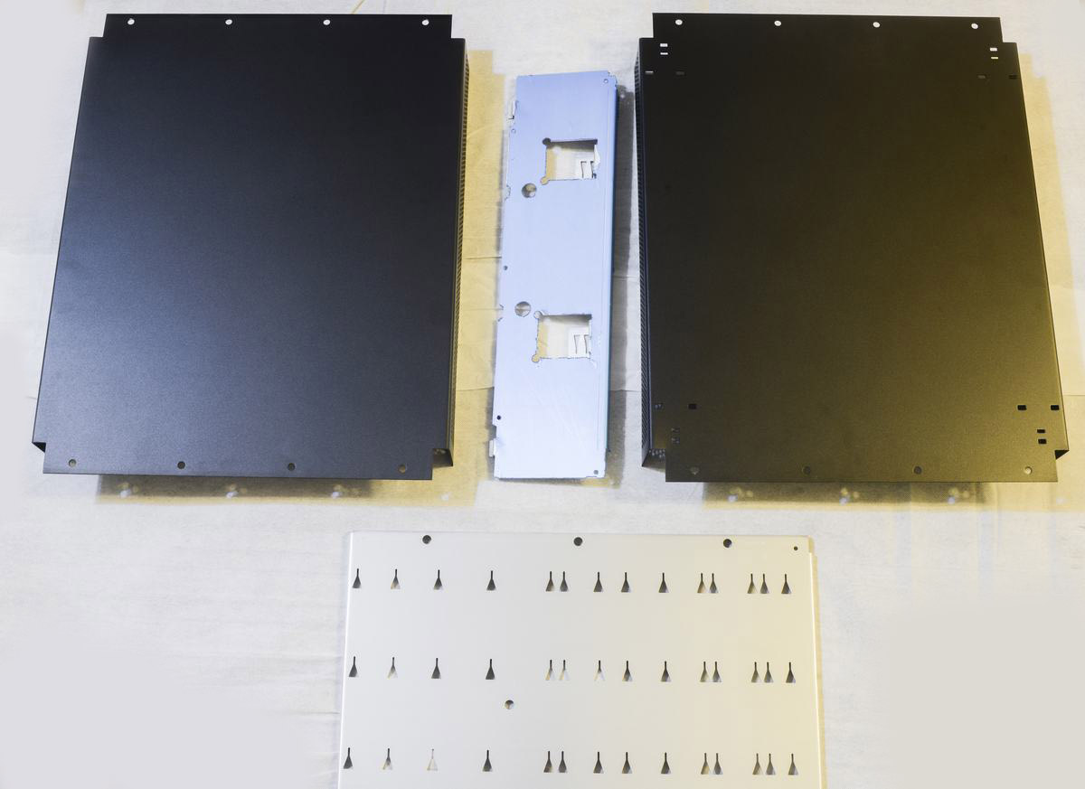
Image 2: Kit version 57xx without chassis frame
Yes, that was a bad joke. Consider everything shown in this article as extreme deep-dive tour into precision analog electronics design. This is what I consider this investment is about, and chance of getting operational calibrator in the end is just a possible by-product bonus outcome, with slim chance of success. If you need 57XX MFC for business purposes, you do not assemble one from scrap, period.
Remember, buying broken or even listed “tested good” used 5700A below market price and fixing it likely will end up as bad expensive exercise, when all hidden costs are considered and accounted for. Paid cost for such a unit WITH proper repair, long-term verification and demanding calibrations will easily exceed cost of buying a fully tested and calibrated unit from reputable source/distributor. So even if you buy complete calibrator for $5K, you can be easily be rewarded with just pile of unstable/non-fixable parts that would need another $XXK to get even just working again, leave alone meeting specifications.
Disclaimer
Redistribution and use of this article, any parts of it or any images or files referenced in it, in source and binary forms, with or without modification, are permitted provided that the following conditions are met:
- Redistributions of article must retain the above copyright notice, this list of conditions, link to this page (https://xdevs.com/article/hulk/) and the following disclaimer.
- Redistributions of files in binary form must reproduce the above copyright notice, this list of conditions, link to this page (https://xdevs.com/article/hulk/), and the following disclaimer in the documentation and/or other materials provided with the distribution, for example Readme file.
All information posted here is hosted just for education purposes and provided AS IS. In no event shall the author, xDevs.com site, or any other 3rd party, including Fluke be liable for any special, direct, indirect, or consequential damages or any damages whatsoever resulting from loss of use, data or profits, whether in an action of contract, negligence or other tortuous action, arising out of or in connection with the use or performance of information published here.
If you willing to contribute or add your experience regarding instrument repairs or provide extra information, you can do so following these simple instructions
Manuals and documentation
Fluke does provide all main manuals, including service information for these older calibrators, right on the product page, without requirement of any registration or access requests, unlike Tektronix or Keysight web-sites. Thumbs up for Fluke, way to host the data on your product page, not hiding behind registration forms, “ask a consultant” or other big-dollar marketing obscurity.
Brochure: The 5700A/5720A MFC: Taking Accuracy to New Level
Fluke 5700A/5720A Series II Operator Guide, May 1996, Rev.1
Fluke 5700A/5720A Series II Operators Manual, May 1996, Rev.2
Fluke 5700A/5720A Series II Operators Manual Supplement, Feb 2008, Issue 5
Fluke 5700A/5720A Series II Operators Manual Supplement, Feb 2008, Issue 9
Fluke 5700A/5720A Series II Service Manual, Nov 2007 w/o schematics
Fluke 5700A/5720A Series II Service Manual Supplement, Issue 6
Fluke 5700A/5720A Series II Service Manual Supplement, Issue 9
Fluke 5700A/5720A Series II Getting started, March 2002, Rev.2
Fluke 5700A/5720A Series II Getting started Supplement, Issue 6
Fluke 5700A/5720A Series II Remote Programming Reference Guide
Fluke 5700A Instrument Security Procedures
Fluke 5720A Instrument Security Procedures
Fluke 5725A Instrument Security Procedures
Fluke 5725A Getting Started, April 2014
Fluke 5725A Getting Started Supplement, Issue 3
Fluke 5725A Instruction Manual, Jan 1989 Rev.7
Fluke 5725A Instruction Manual Supplement, Issue 4
Fluke 5725A Instruction manual
Tech data: 5700A->5720A Upgrade Service
Model 5440A-7002 Low Thermal Test Lead Set – Specification
Fluke 5700A, 5720A CE Declaration of Conformity
Service notes
First goes the most important document for repairs/maintenance – 570-page service manual. Credits for hosting it first going to KO4BB portal. We are lucky to also have schematics, list of parts, assembly drawings of the boards included in it!
Fluke 5700A MFC Service Manual with schematics, Rev.9,3/96, March 1996
Fluke 5700A Series II/5720A MFC Service Manual with schematics, Rev.1,3/02, June 1996
5700A Series I and 5700A/5720A Series II difference
According to An evaluation of the 5700A Series II Artifact Calibration document, major changes in Fluke 5700A/5720A Series II are related to Artifact Calibration and high-frequency AC voltage. Artifact Calibration was improved on a number of ranges, to minimize biases. A new interpolation algorithm is also used for lower ACI ranges to provide better performance.
From hardware standpoint, Model 5720/5700 Series II calibrator has a modification to the in-guard microprocessor circuitry and firmware to minimize noise in the low millivolt DC ranges. Also, because of the tighter specifications of the 5720A, there are more carefully selected components, than in the standard 5700A. Lot of circuit tweaks and changes are on A11 REFDAC and A16 Power Amplifier inguard assembly modules. Many tweaks and minor changes on every board in 5720A level hardware address better reliability and stability of the calibrator. Digital processor board A20 firmware are also updated as a result to reflect added functionality.
Project concept and workflow
Where do we start with huge build project like this? Good starting point will be evaluating what is required to get minimum functional configuration, and acquire all required modules. Once that goal is achieved, we can focus on extra functions and more tests, related to each domain and piece of the calibrator. Since we getting junk boards in unknown conditions, each module and assembly must be carefully tested and verified before even considered working good.
Keeping track on action items, understanding of the overall building blocks and 5700A calibrator architecture is very important. For this reason we try to document timing and test procedures in the project as well. It took multiple years to collect all bits and pieces, without any specific order or sequence. This article re-structured not in the order how we worked on each assebmly/part but rather in design perspective from bare metal frame to minimal function set to complete fully-stuffed unit. If you interested in more specific aspect or assembly, feel free to navigate with index in the article head.
Over the course of the project author and other members of xDevs community have learned a great lot about inner workings and troubleshooting non-obvious soft-failure issues, such as out of specification output drift or excessive noise. We hope to provide great amount of details in this article about 5700A or 5720A, however some of this gained knowledge is restricted to internal use and will not be published. If you have specific question about 5700A/5720A/5730A you can try asking us online on this page.
Fluke donor chassis. Special Hulk-edition.
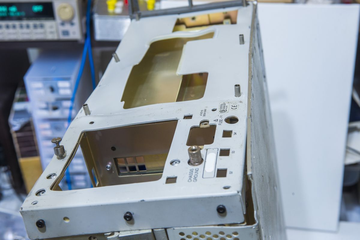
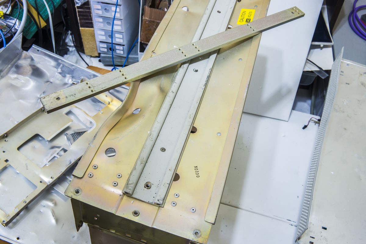
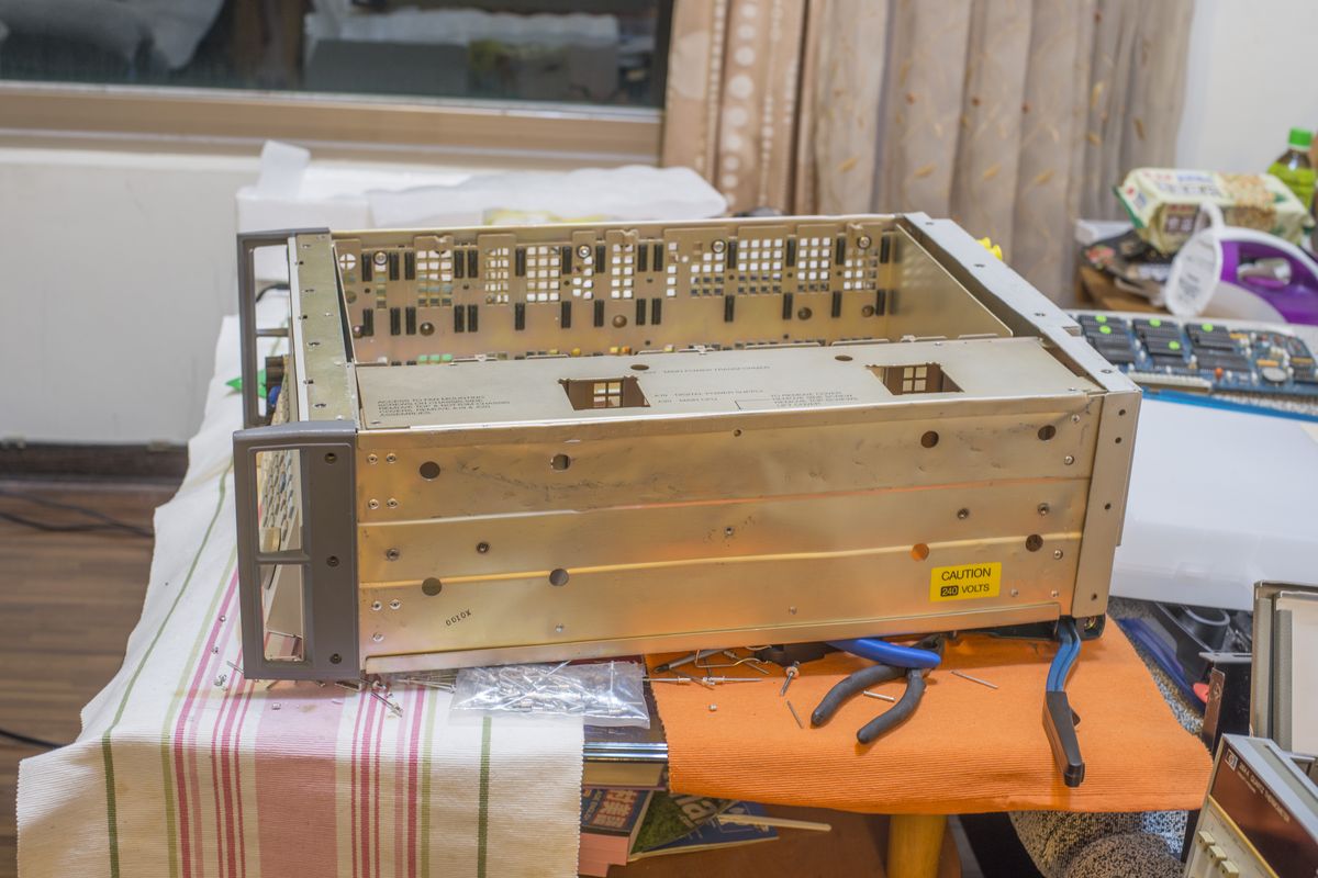
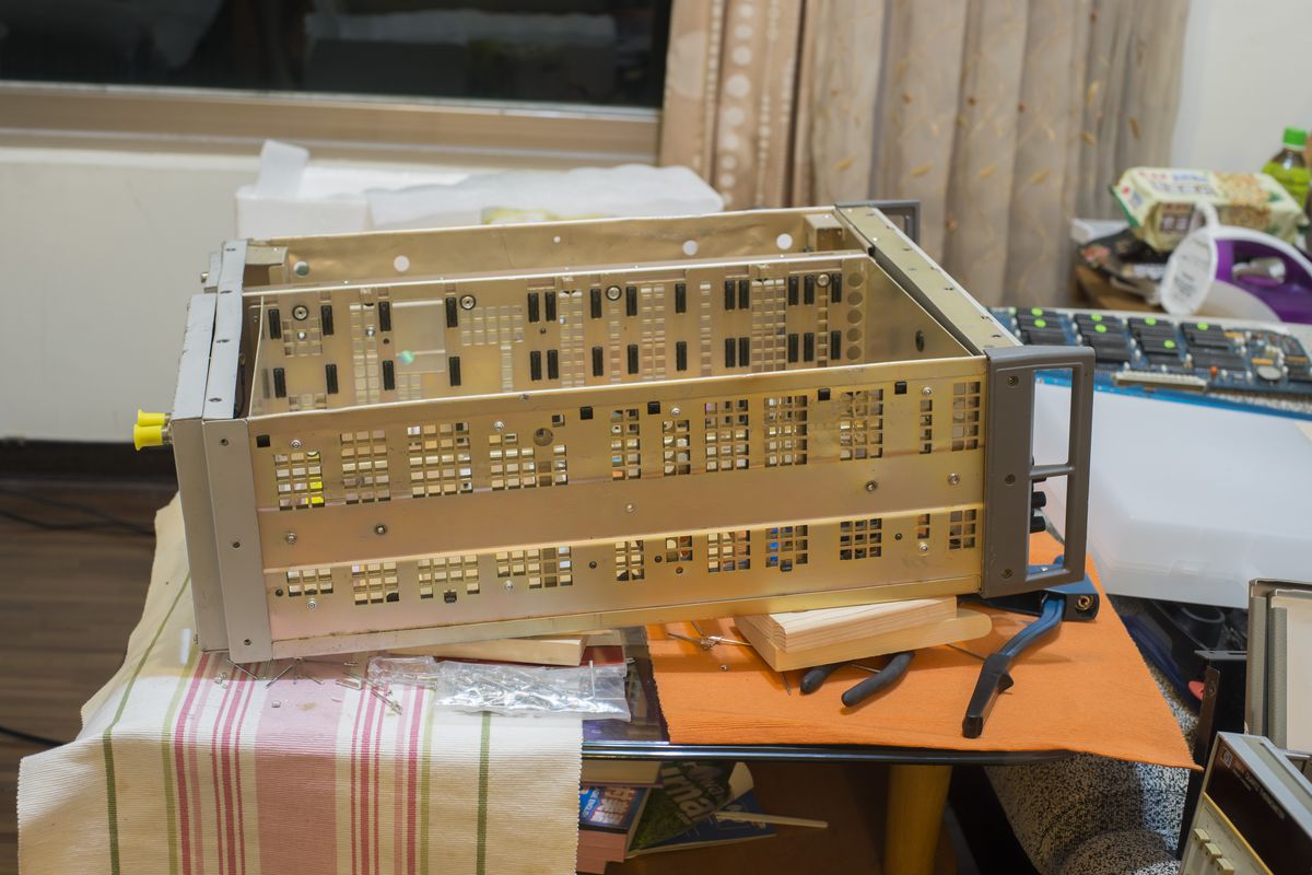
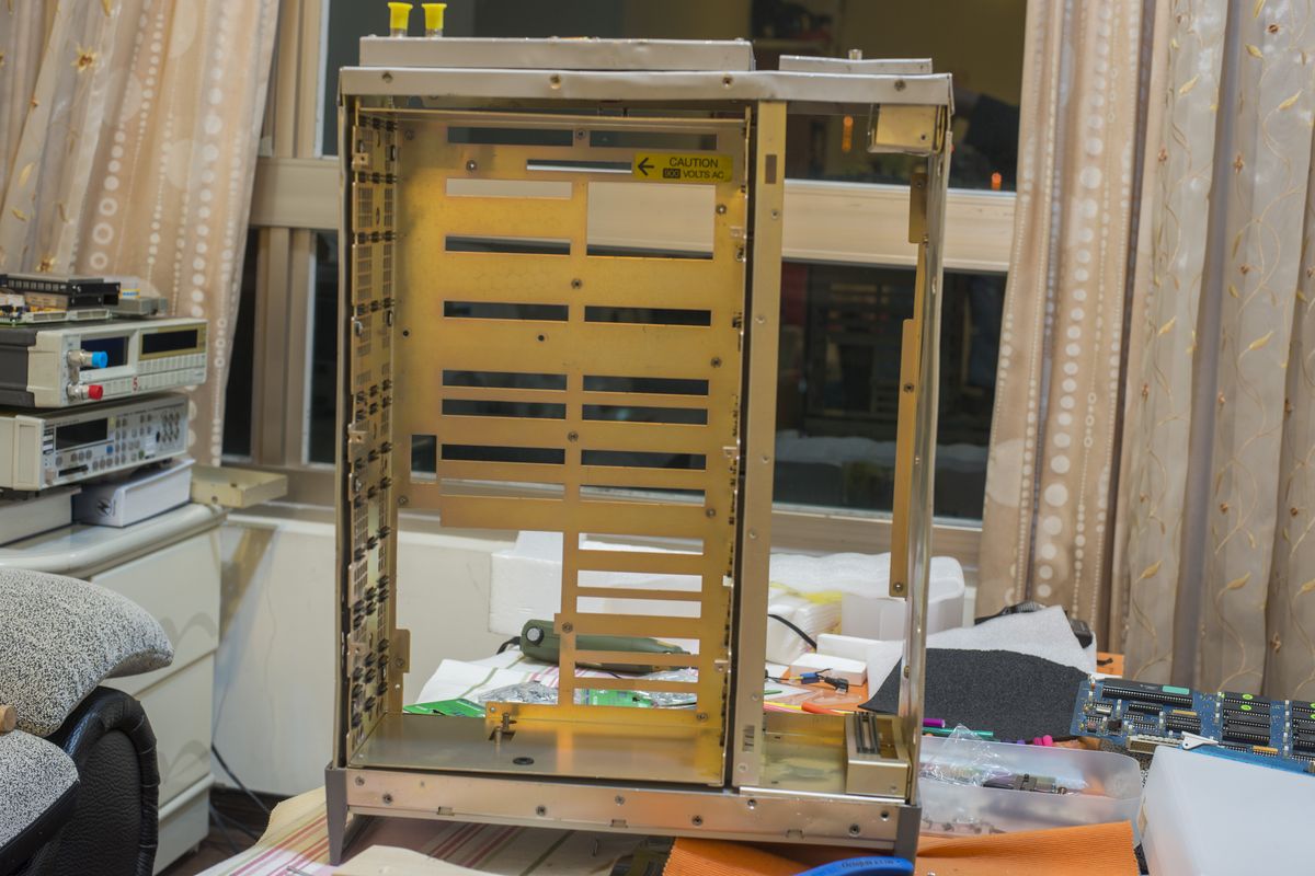
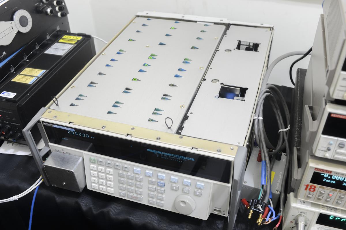
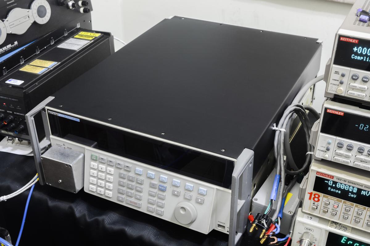
Buying original metal chassis from 5700A series unit was not expected at all, and case to fit all boards and calibrators parts was planned in the end, with fully custom CNC metal work. Such fully custom chassis for all PCBAs, resembling Fluke’s own calibrator design would be a project on it’s own actually. But by the time when all boards were acquired, opportunity to buy empty 5720A chassis arise by a very good friends help. Chassis had just “few dents and scratches”. Nothing to worry about?
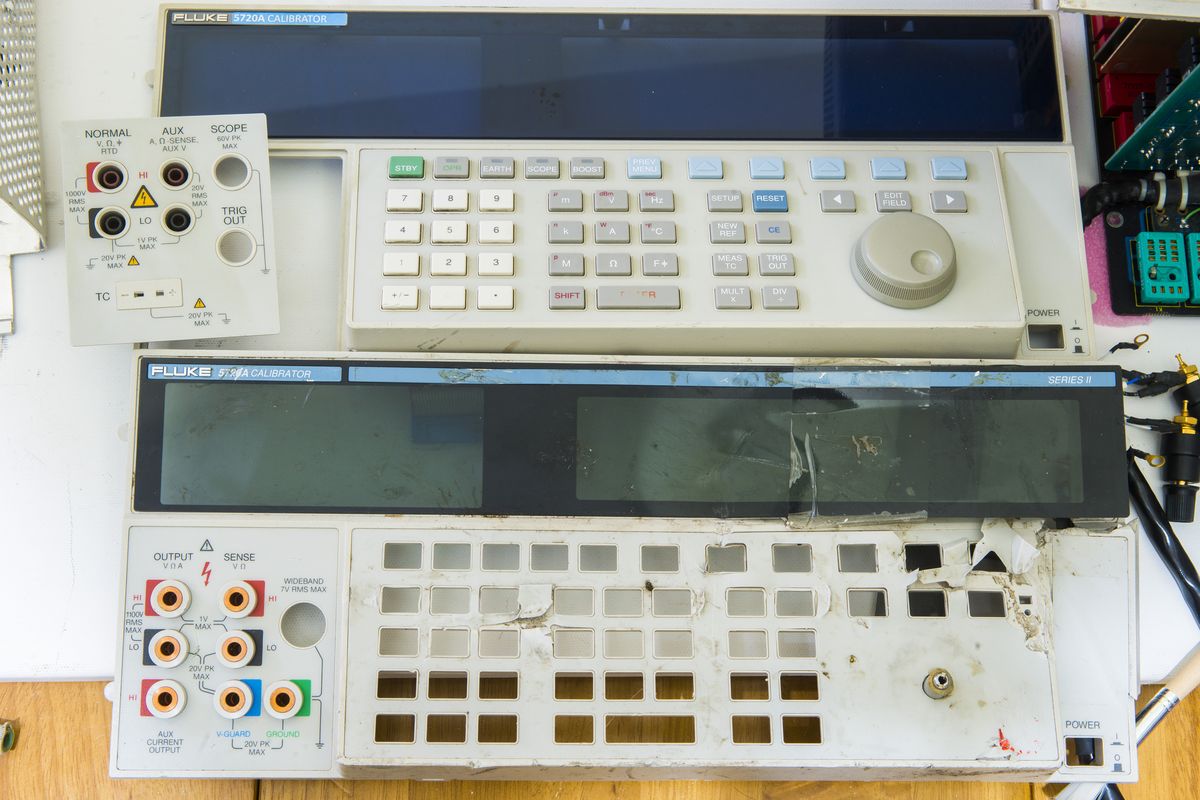
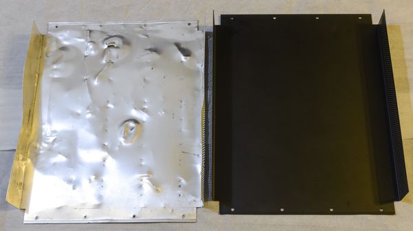
Well, this chassis from donor poor calibrator had some tough life, perhaps “decomissioned” by military. Perhaps not everybody know in 2018 year that smashing hardware does not always erase data?. Or perhaps it was piece of MARVELL’s Avengers movie prop for Mr. Hulk training. Project “DIY 5720A” now officially renamed into “Project Hulk”. :)
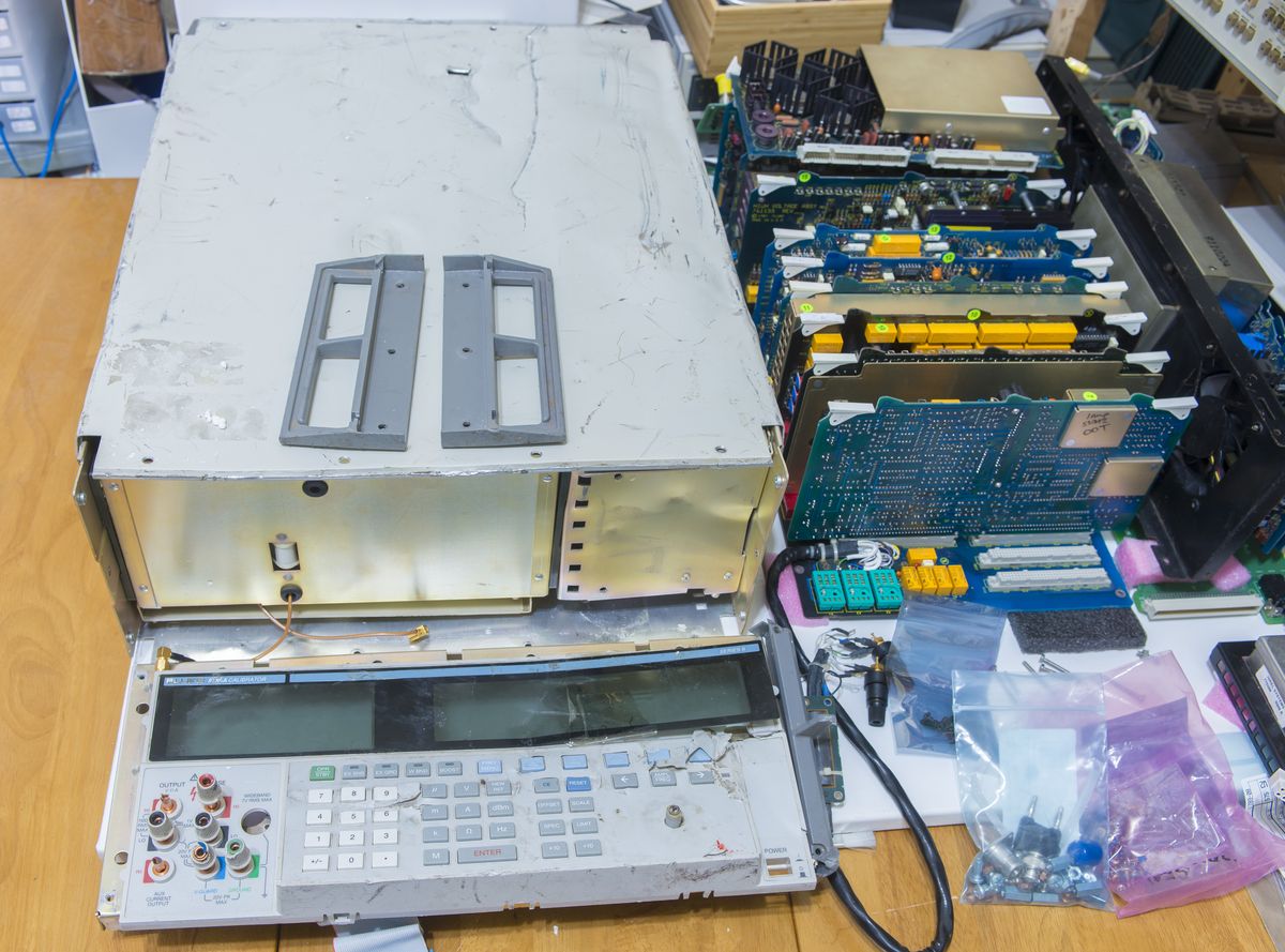
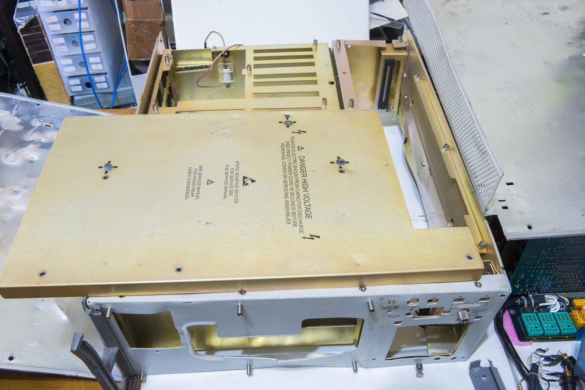
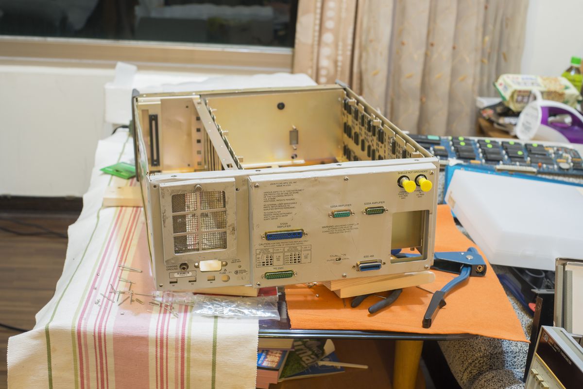
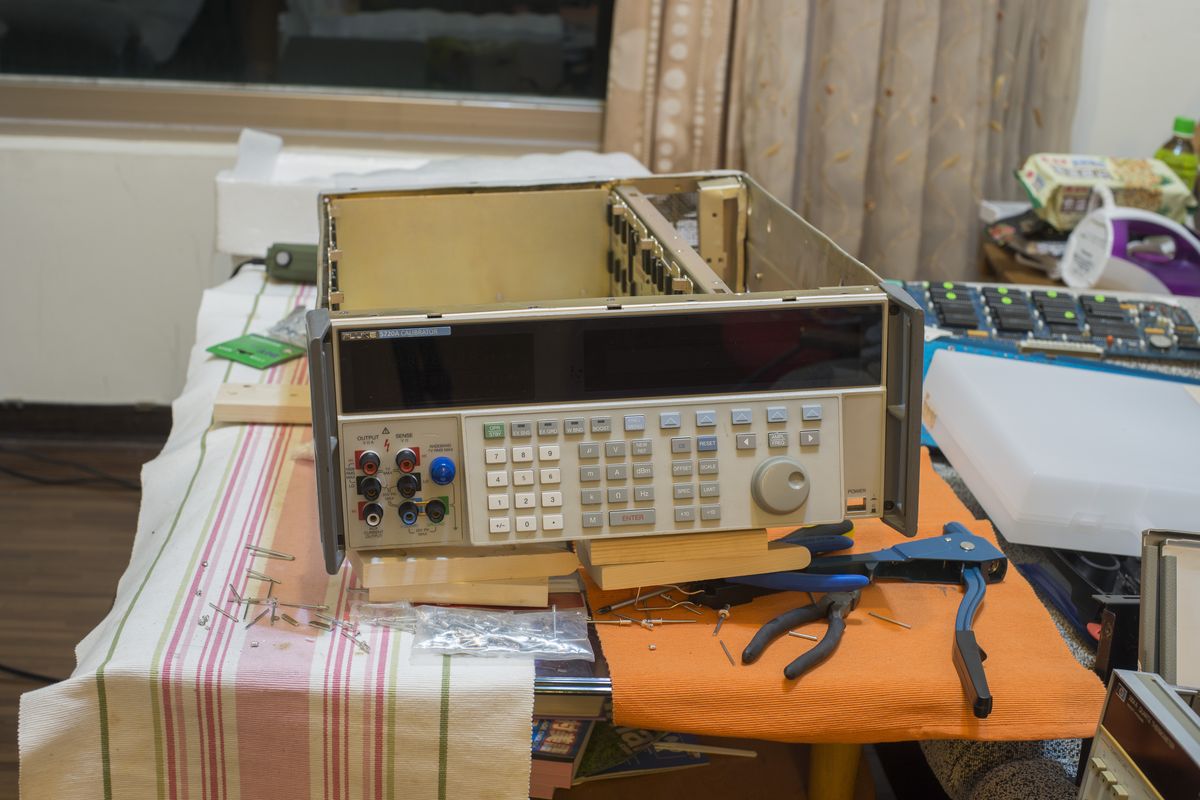
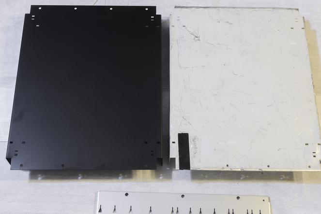
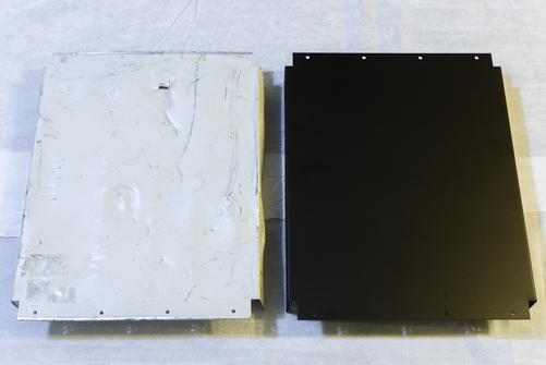
Image 3: Boards on the right should go into smashed chassis on the left
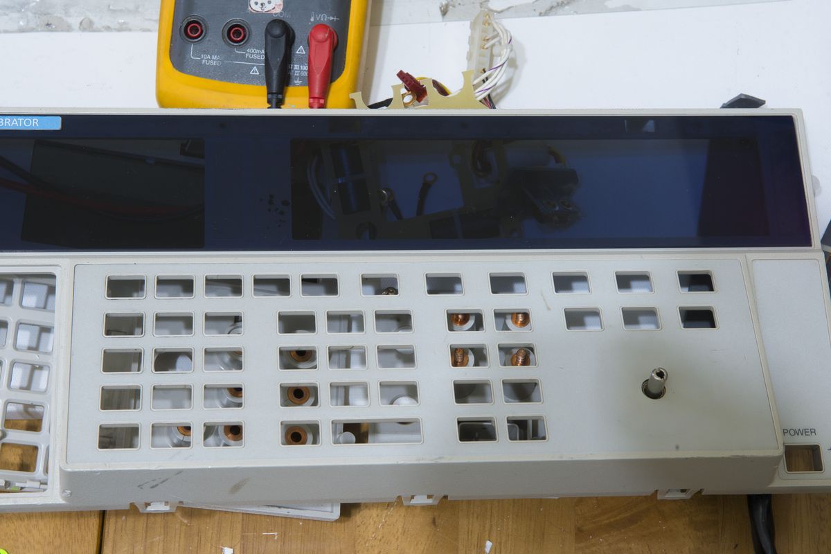
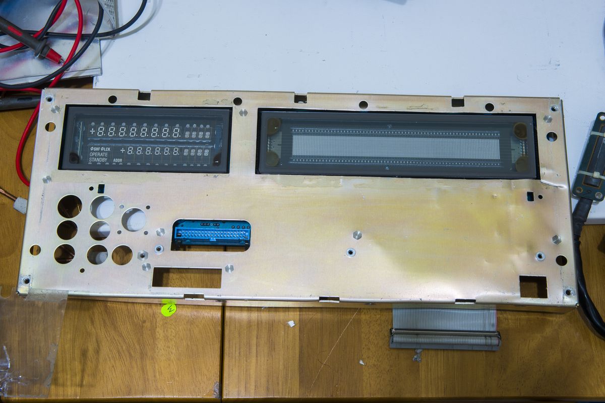
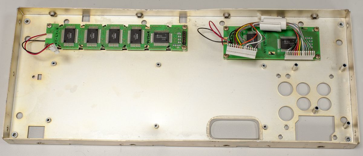
Front panel, custom Fluke binding posts, rear metalwork are all smashed. Top and bottom aluminum covers look like hit by a truck.
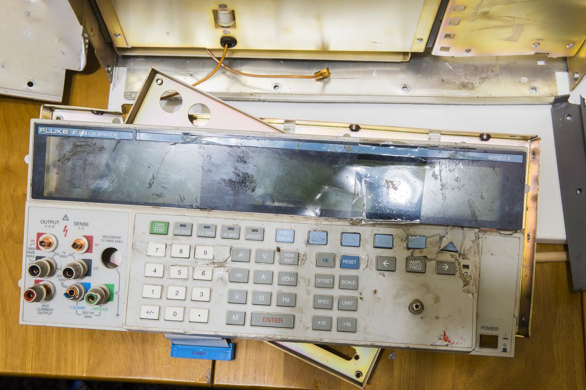
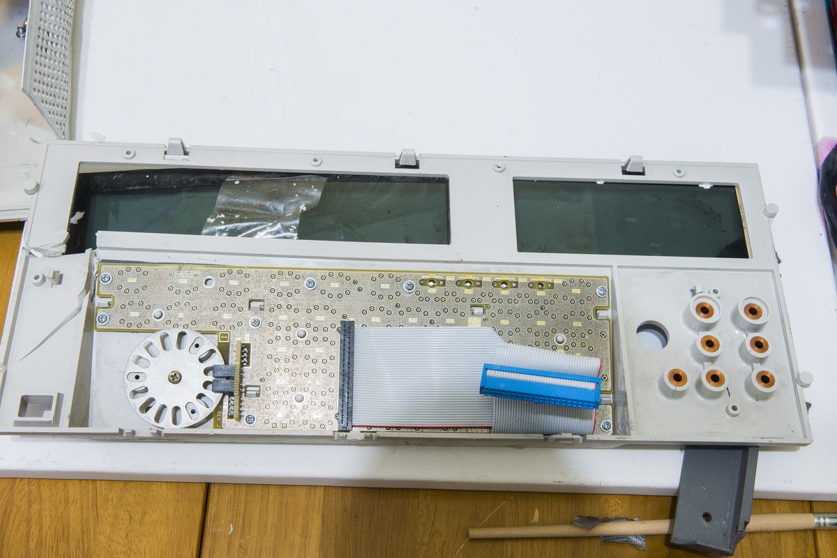
Image 4: Damaged front panel from donor 5720A chassis
Dent in plastic screen lens is so bad, that whole thing must be replaced.
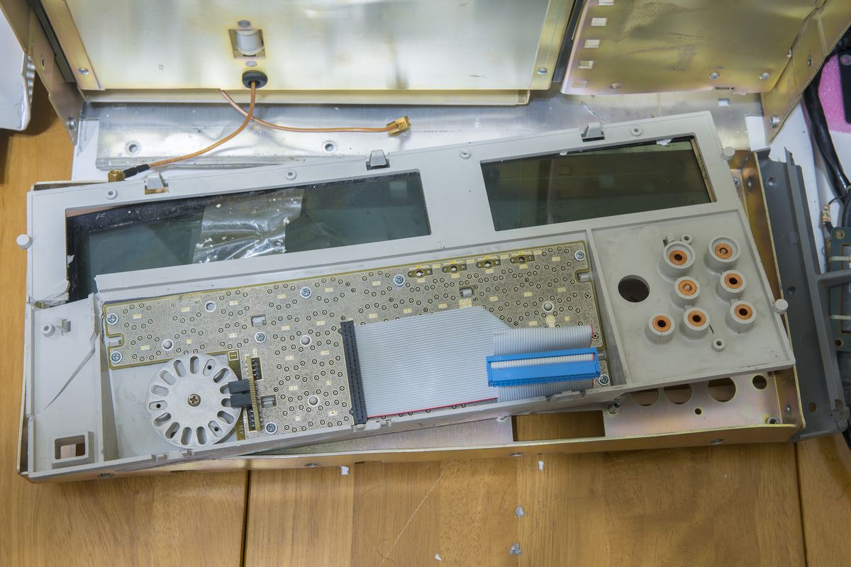
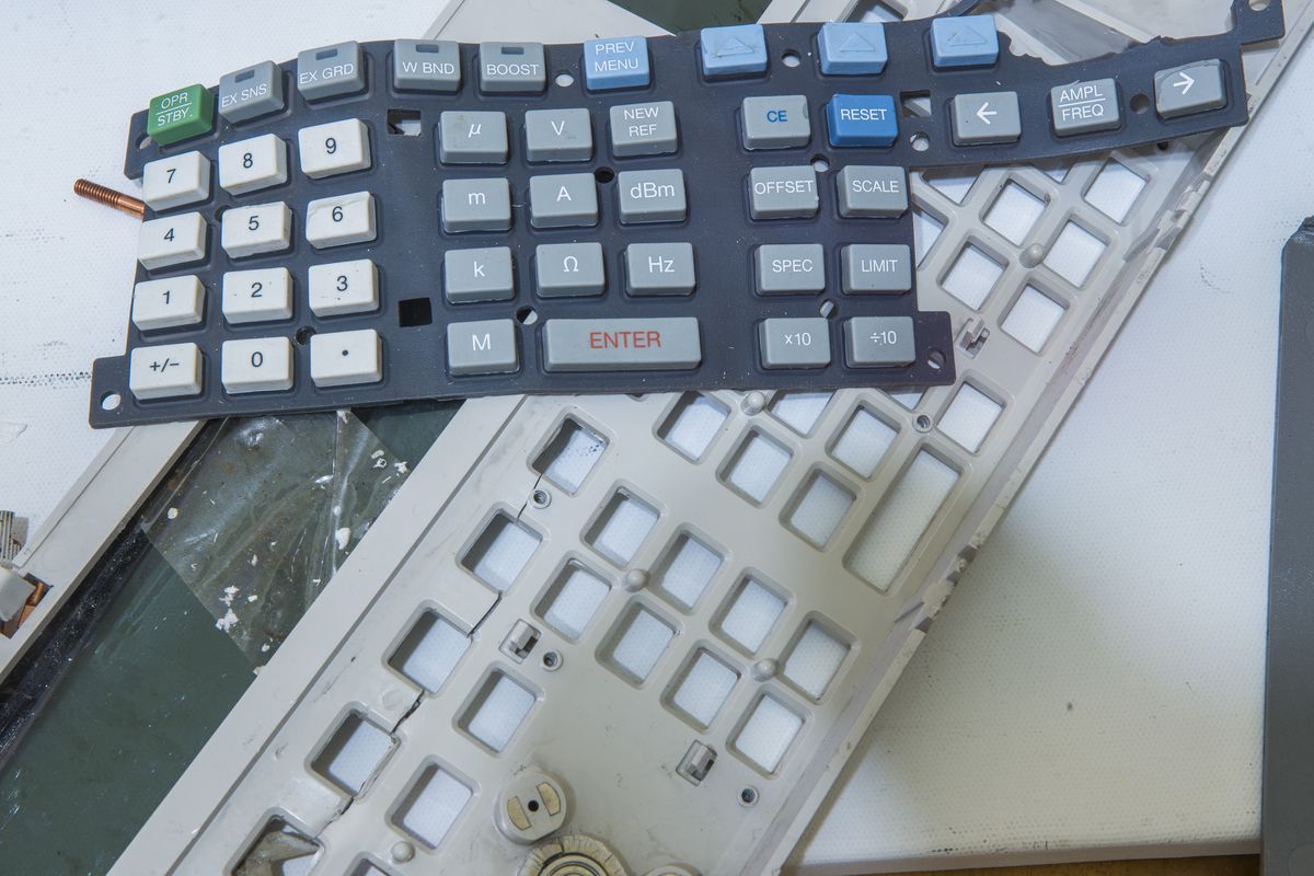
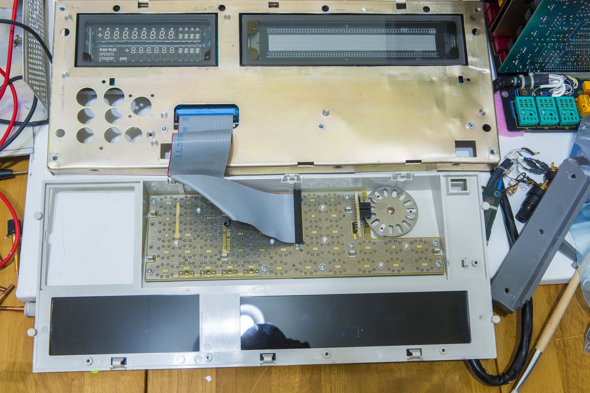
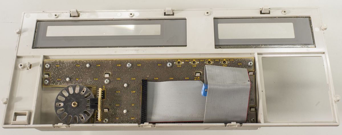
Image 5: But A1 keyboard PCBA survived well
A1 is membrane keyboard assembly, so we can reuse that part in new front panel plastic frame.
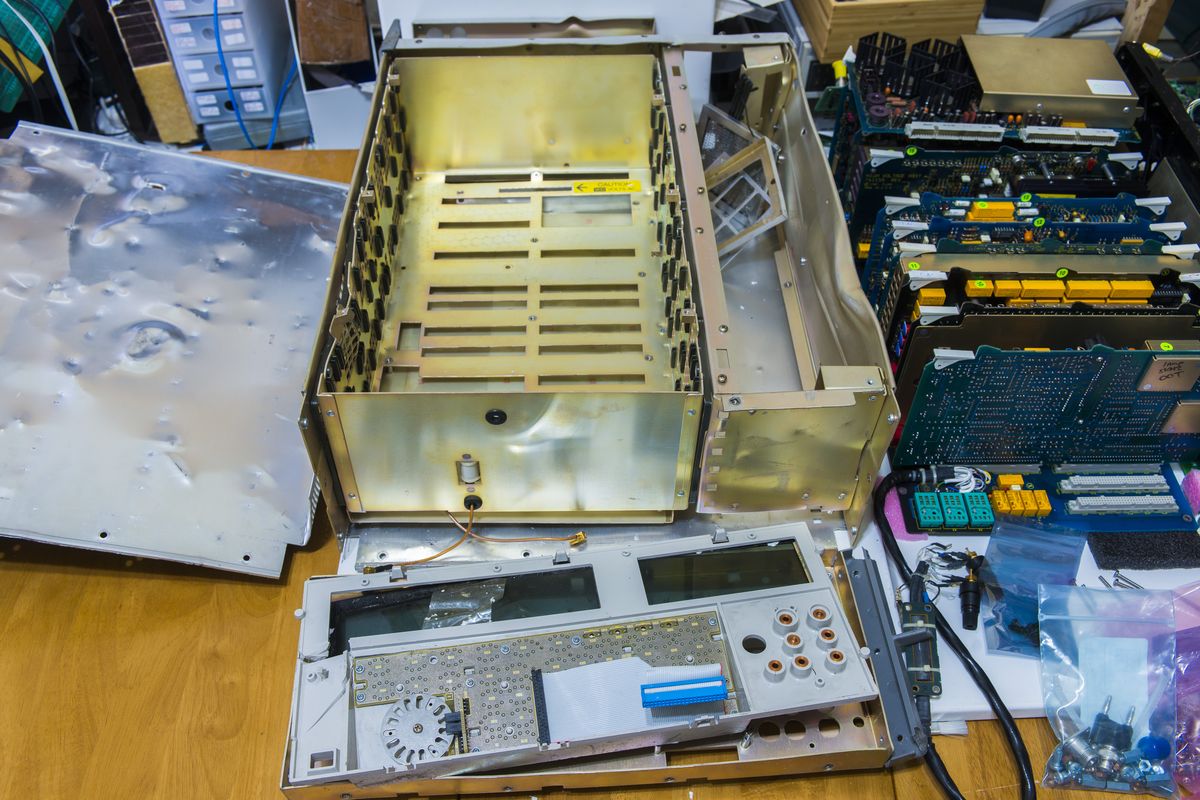
Image 6: Bare frame with covers removed.
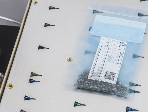
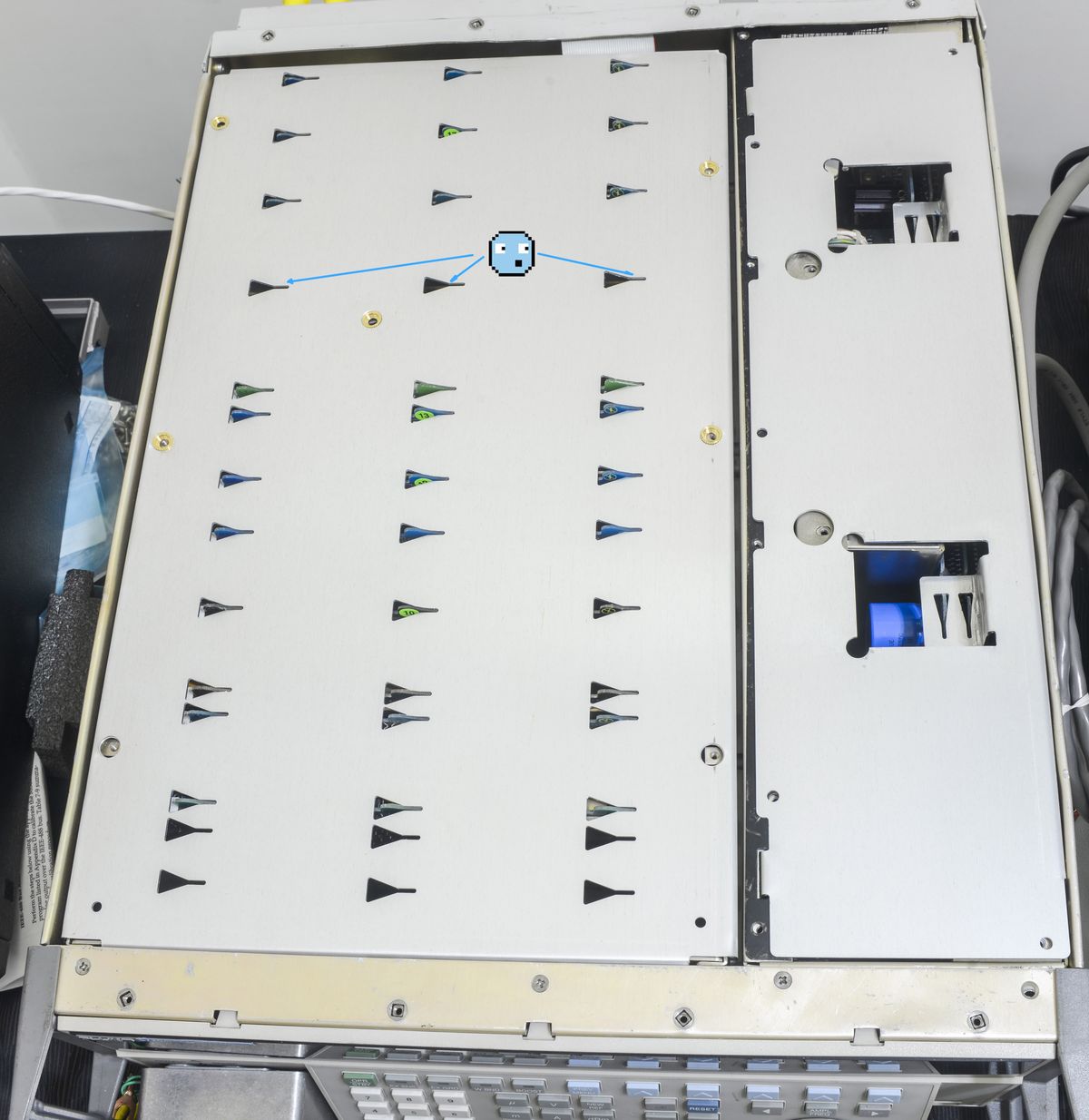
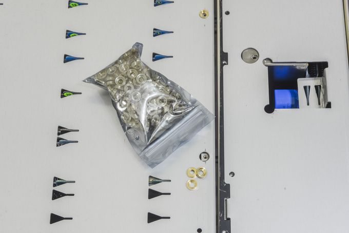
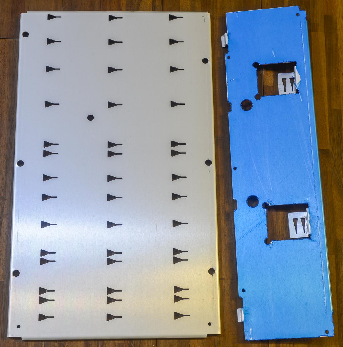
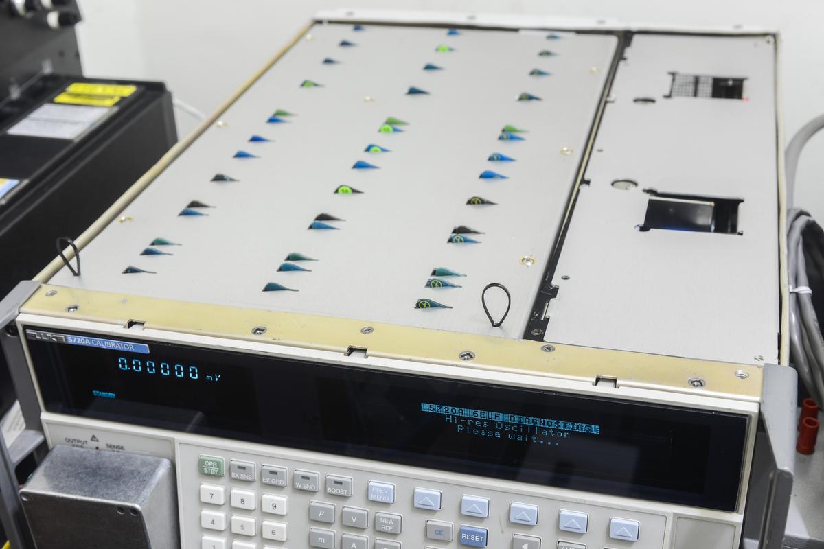
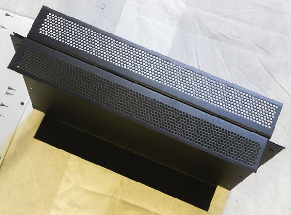
Chassis was sold with missing inguard and outguard top shields. Will have to make custom metal replacement for those.
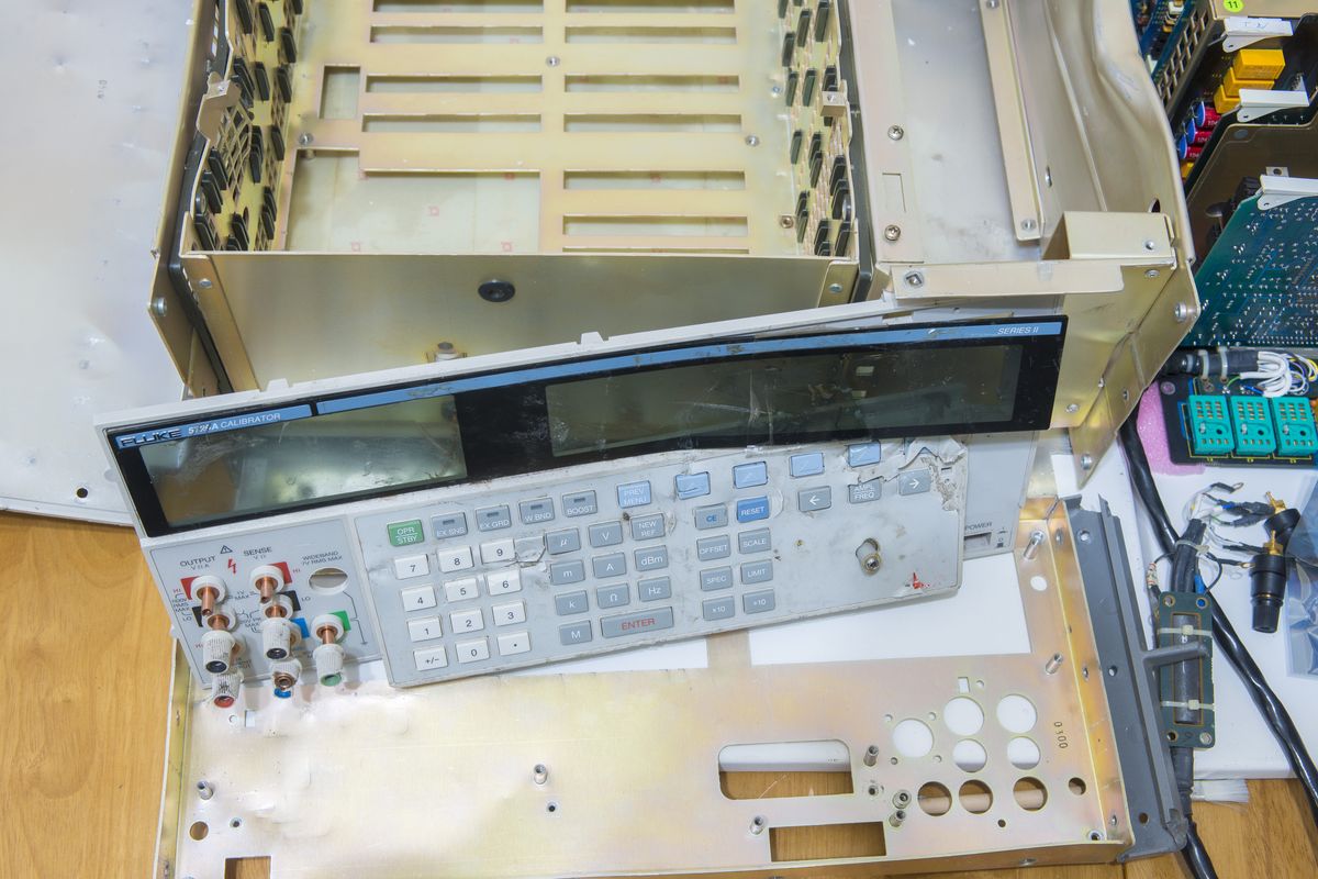
Image 7: Another shot with damaged front panel bezel and chassis
Worth to mention that metal thickness in 57xx series calibrator frames is at least 2 mm thick. Main structural frame is steel frame with mounted mains transformer with inguard and outguard hardware mounted together.
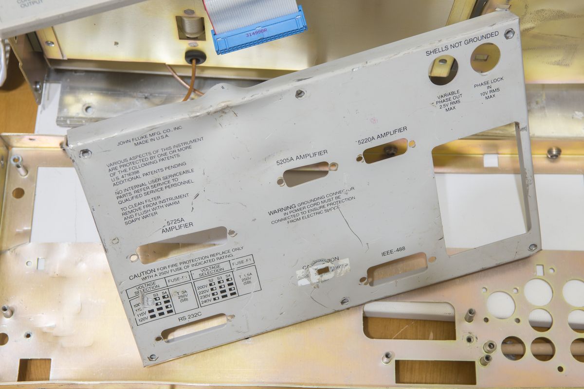
Image 8: Rear panel metal cover
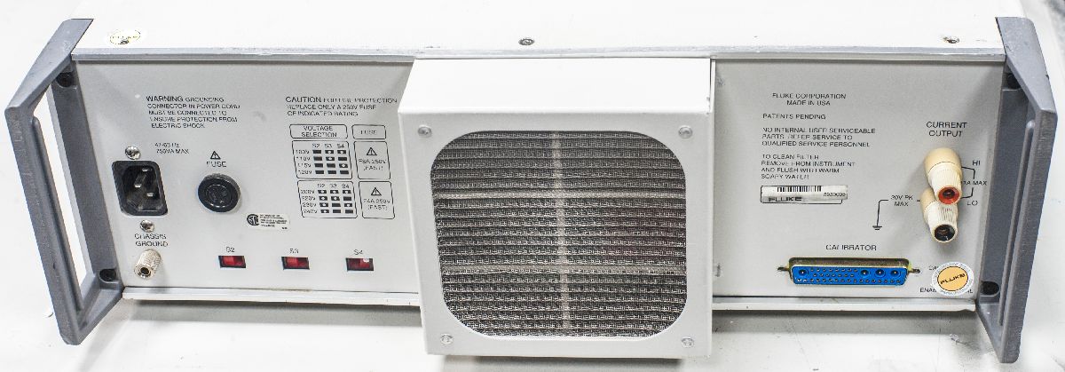
Looking at rear panel we can guess expansion ports available for Fluke 5205A, 5220A and typically used 5725A amplifiers. Communication interfaces are either DB25-style RS-232C or standard IEEE 488 GPIB. Frequency for ACV function output can be locked to external precision clock reference. Also 57xx calibrator can provide precision phase-shift on dedicated variable Phase Out BNC.
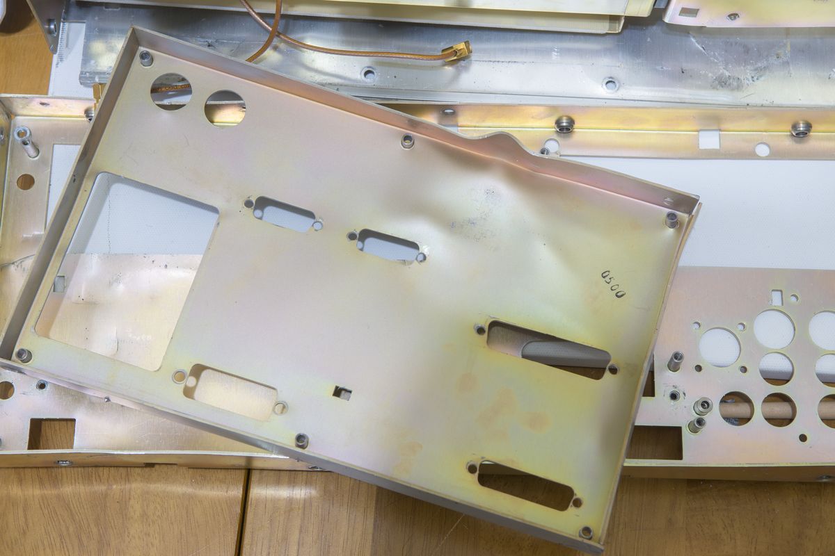
Image 9: Rear panel metal cover, back side
Side walls also damaged. They are mounted with aluminum rivets and have to be removed for metalworking.
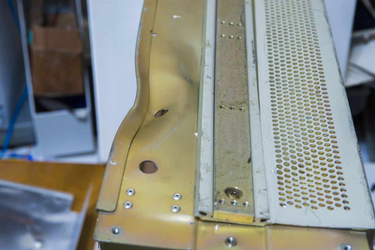
Image 10: Surface flatness and coplanarity are not the words in this chassis
It’ll take quite a bit of effort to make this all able to assemble together.
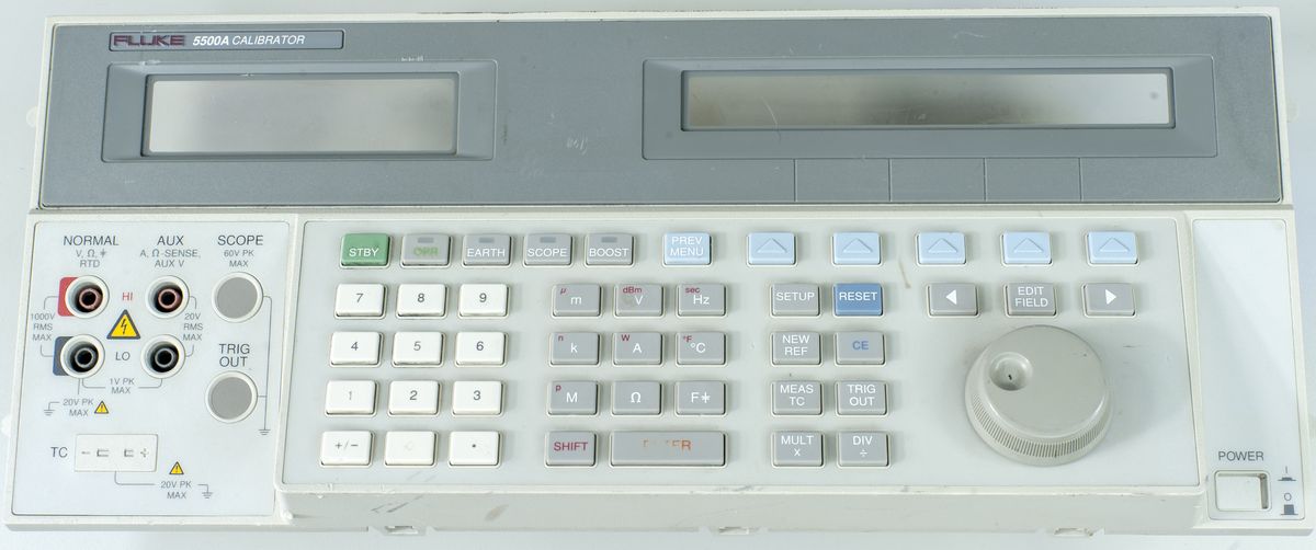
We have some donor plastic handles from Fluke 5500A front panel, that are same as ones used in 5700A.
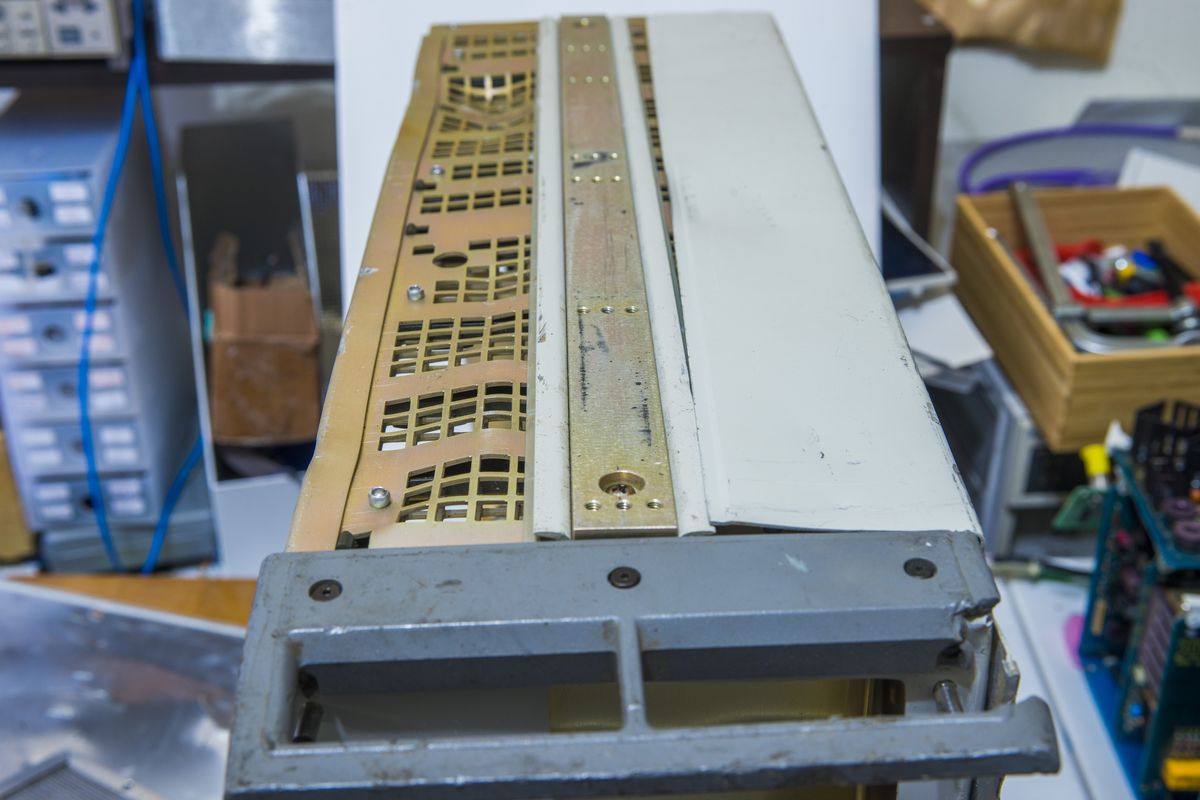
Image 12: Damaged plastic handle
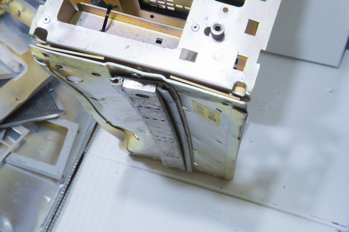
Image 13: These metal surfaces supposed to be straight.
Thick rackmount bars helped to reduce further damage to the side walls. However they will need minor flatness work too.
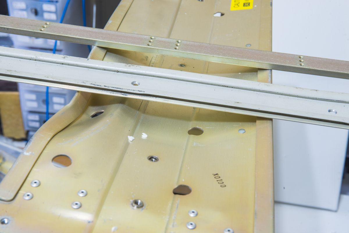
Image 15: Metalwork surface curvature
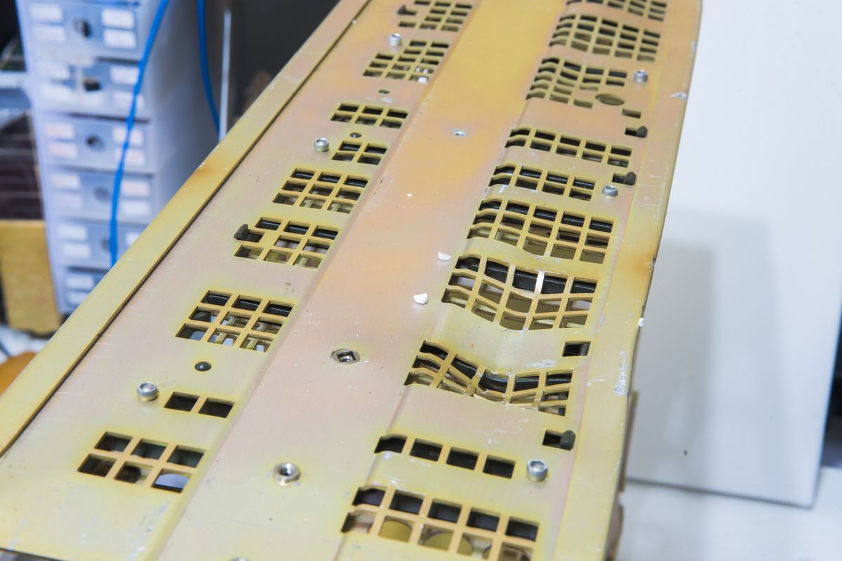
Image 16: Side wall damaged towards isolated inguard frame
Inguard frame does not look very bad, so only minor hammer work will be needed here.
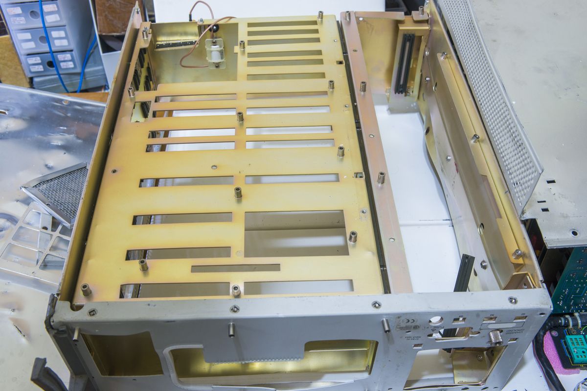
Image 17: Bottom side with inguard frame
To protect bottom side of the A3 motherboard metal shield covers most of it. This part we can reuse with minor effort.
Inner surface of the bottom shield is covered with fiberglass PCB material without any copper foil. Since A3 board can carry voltages up to 1.1kV with frequency up to 100kHz this insulation layer is important.
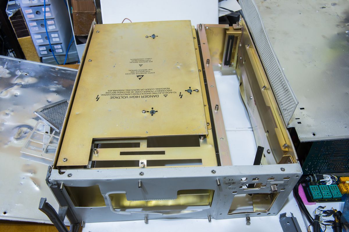
Image 19: Bottom shield in place
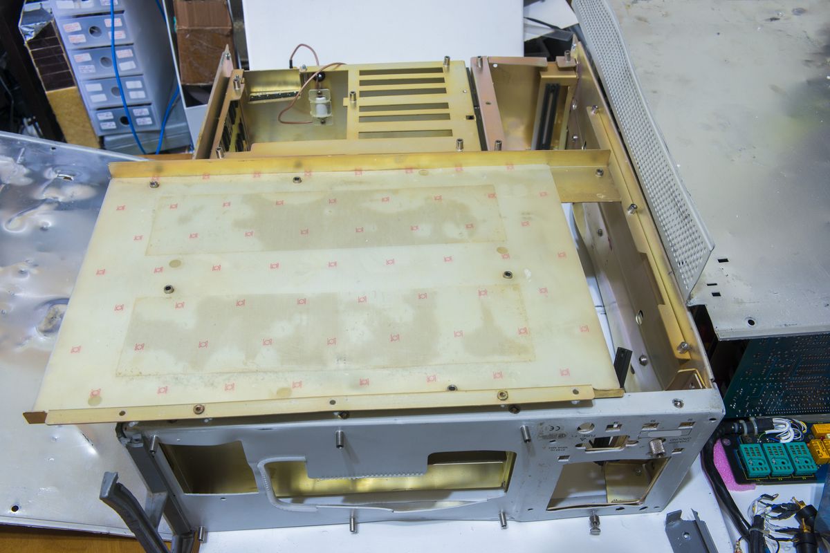
Image 20: Bottom shield for inguard motherboard, isolation PCB layer
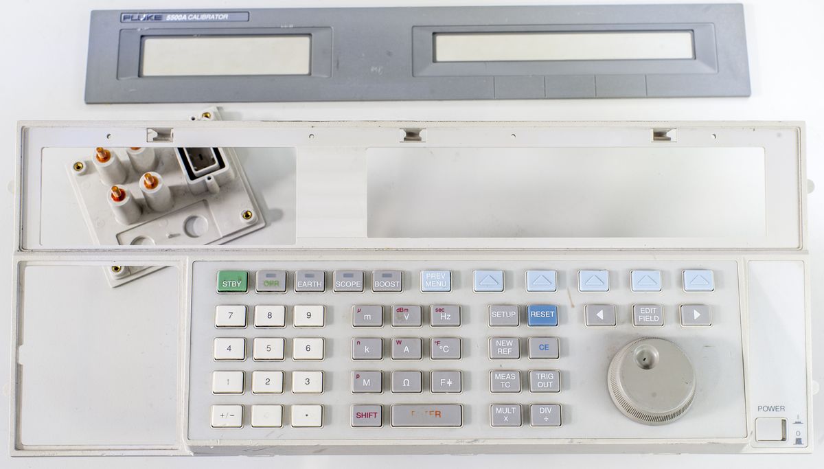
Time to reuse spare Fluke 5500A front panel parts to merge two pieces into workable front panel.
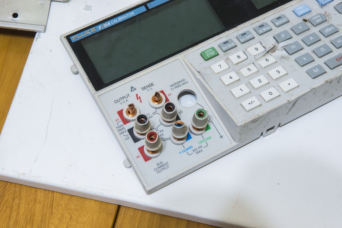
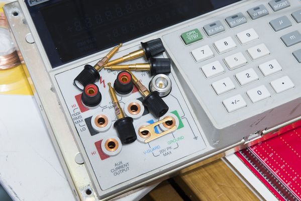
Image 21: Damaged Fluke low-thermal 5-way binding posts
Posts carefully removed, revealing copper contact blocks embedded into front panel plastic frame.
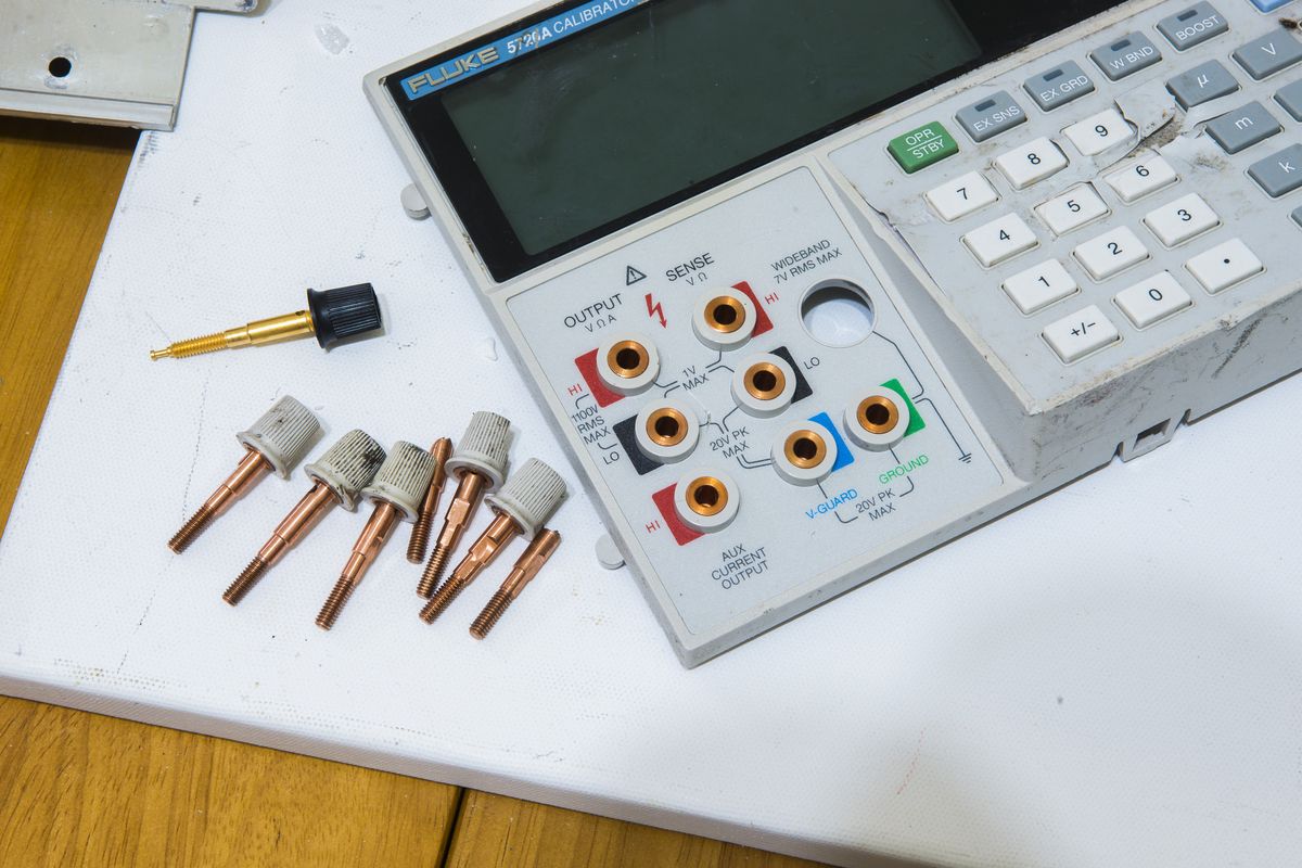
Image 22: Post studs are removed out of the panel
Idea is to remove posts block section and integrate it into our good Fluke 5500A panel.
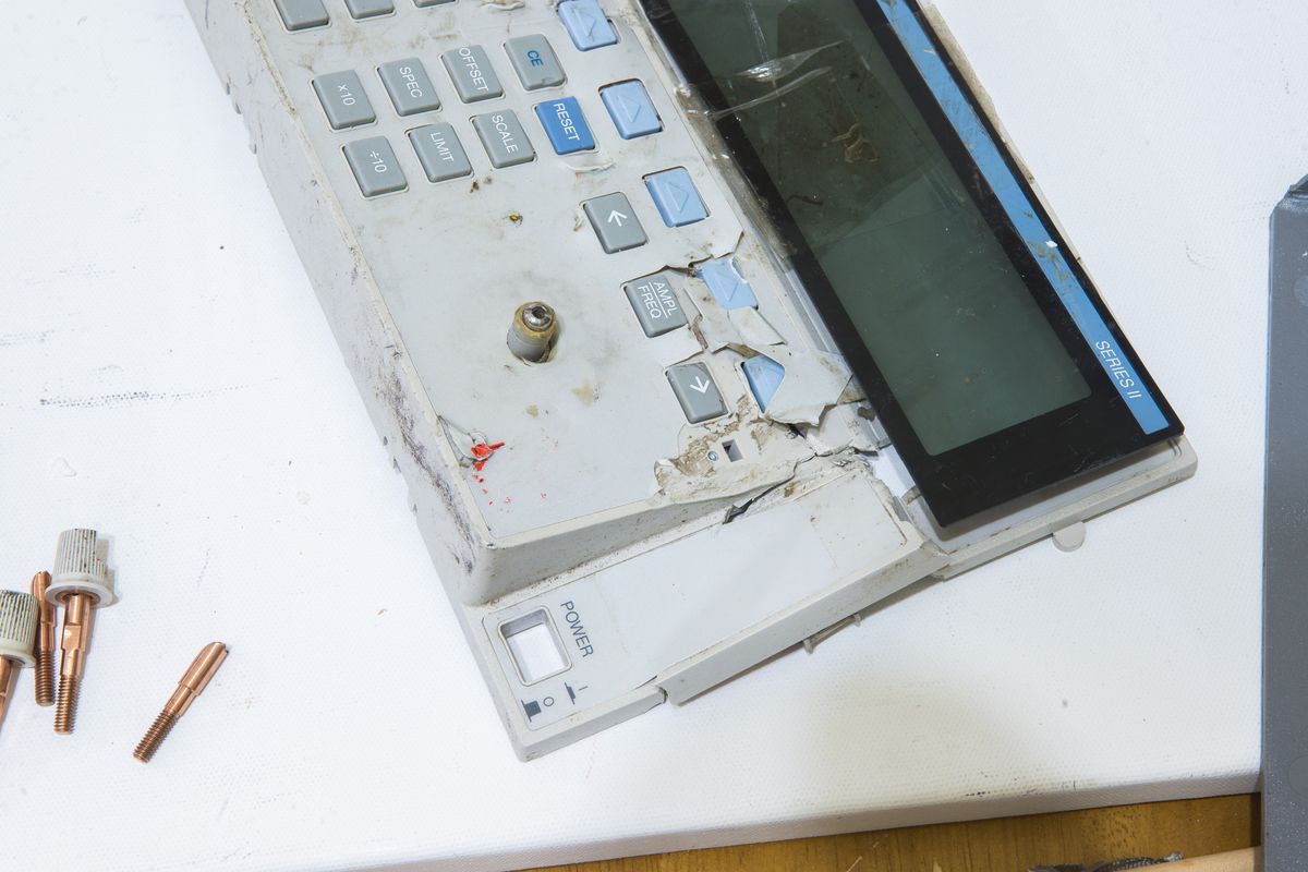
Image 23: Right side of the plastic panel seriously damaged, with pieces missing
We will reuse A1 keyboard PCBA from this chassis onto new frame. Lucky for us, board is not damaged.
Plastic around copper terminals have cracked, but we can fix that with some bond glue.
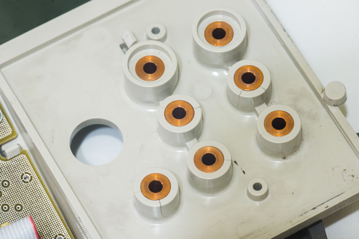
Image 25: Copper terminals overview
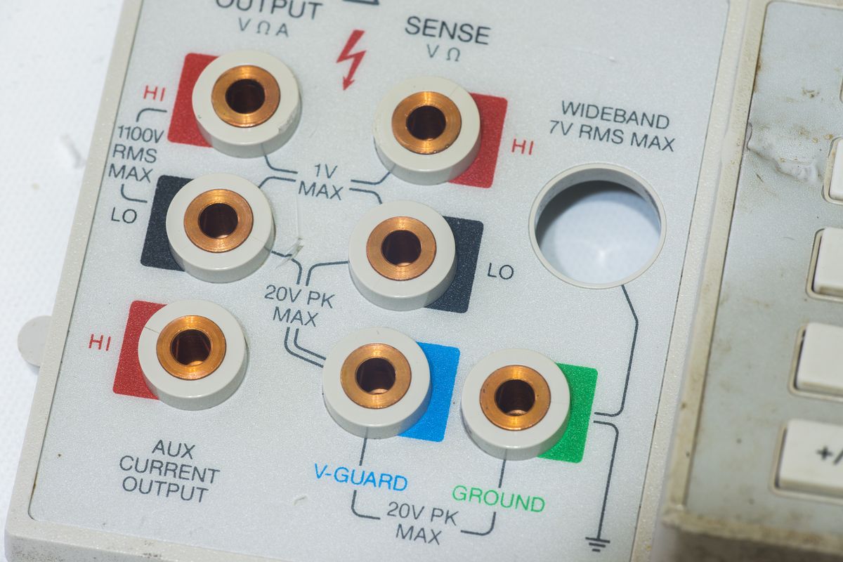
Image 26: Close-up on front side of the terminals
For binding posts I have an idea how to make it all work..
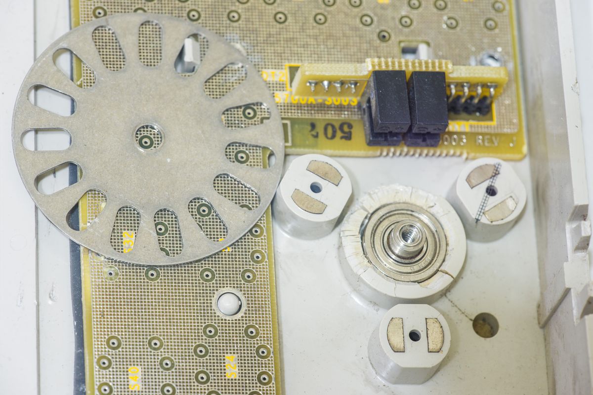
Image 27: Encoder mechanism with optical detector assembly.
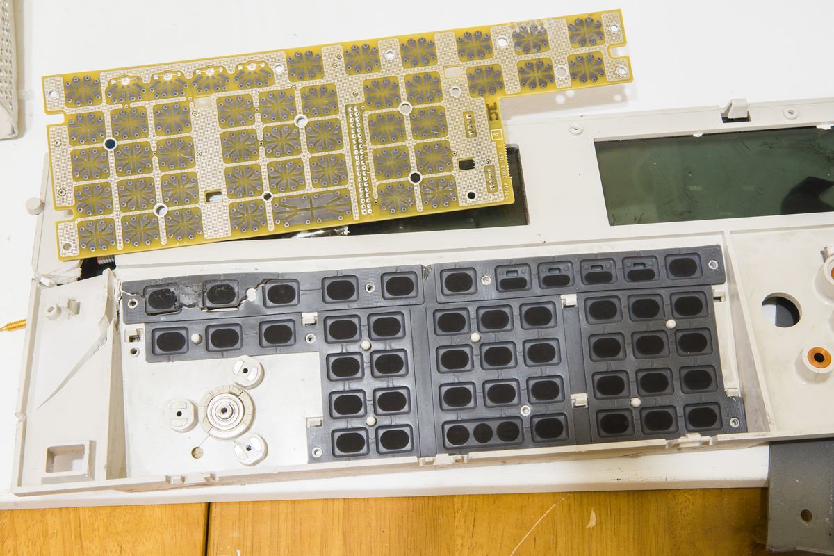
Image 28: A1 Keypad PCBA and rubber membrane keys
Will need to reuse pieces of 5500A membrane to restore the original keypad looks. Most of keys are same, but positions are different.
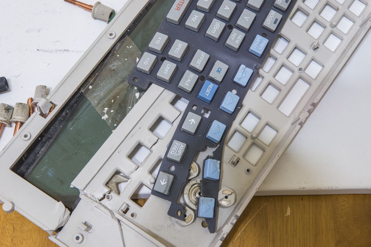
Image 29: Some of the keys are damaged and torn
Should be easy to do with precision knife work and some patience.
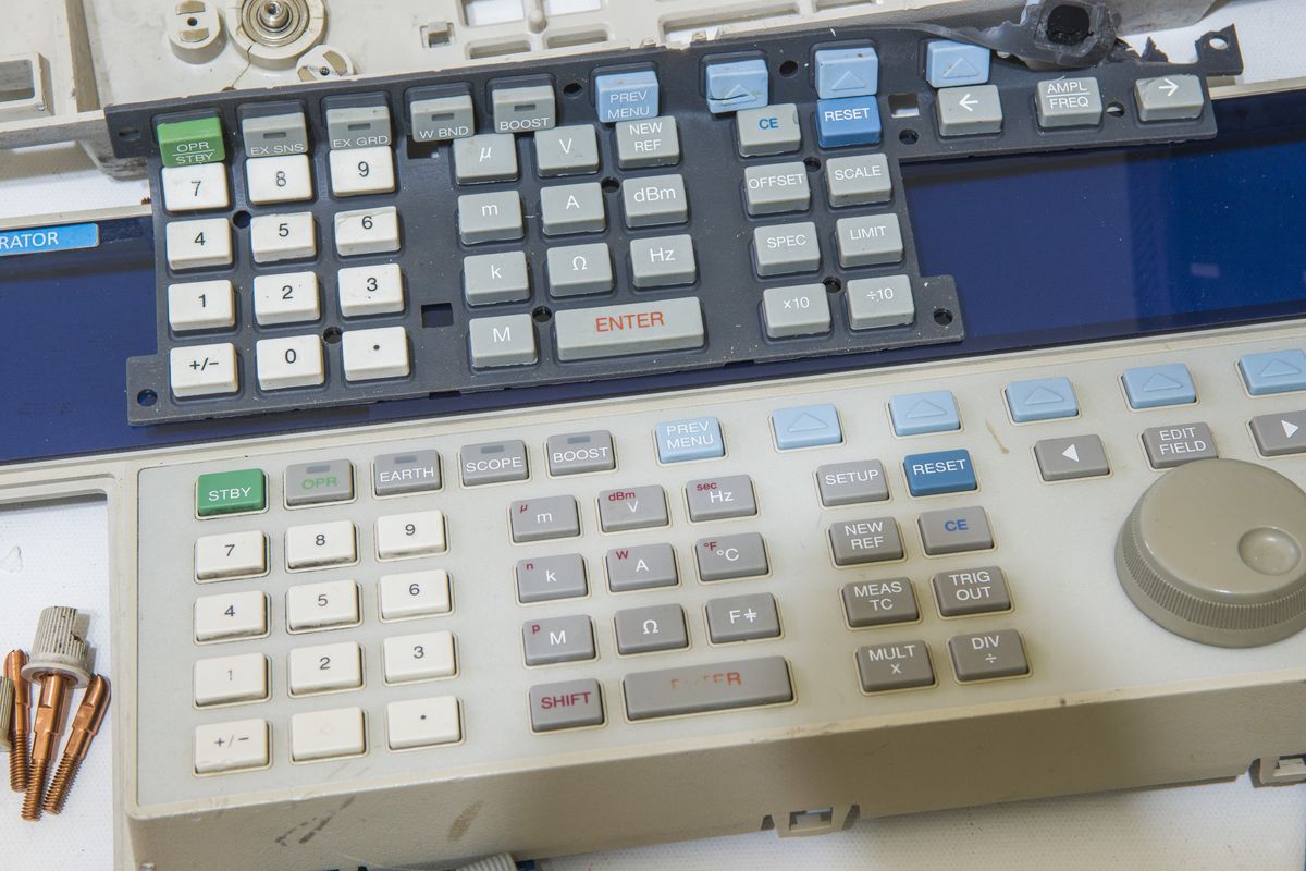
Image 30: Comparison between Fluke 5720A and Fluke 5500A keypads
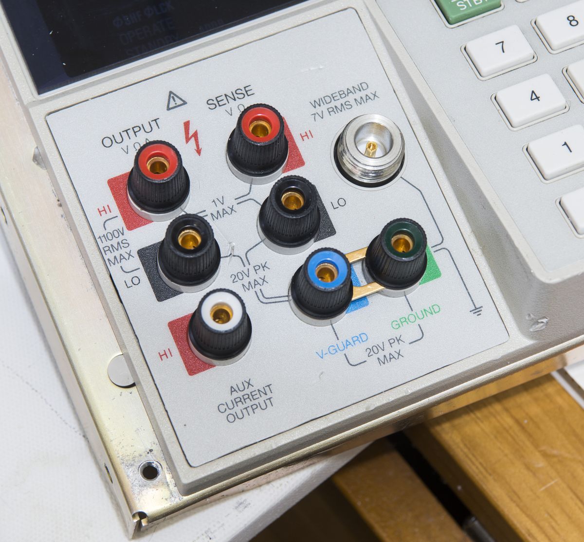
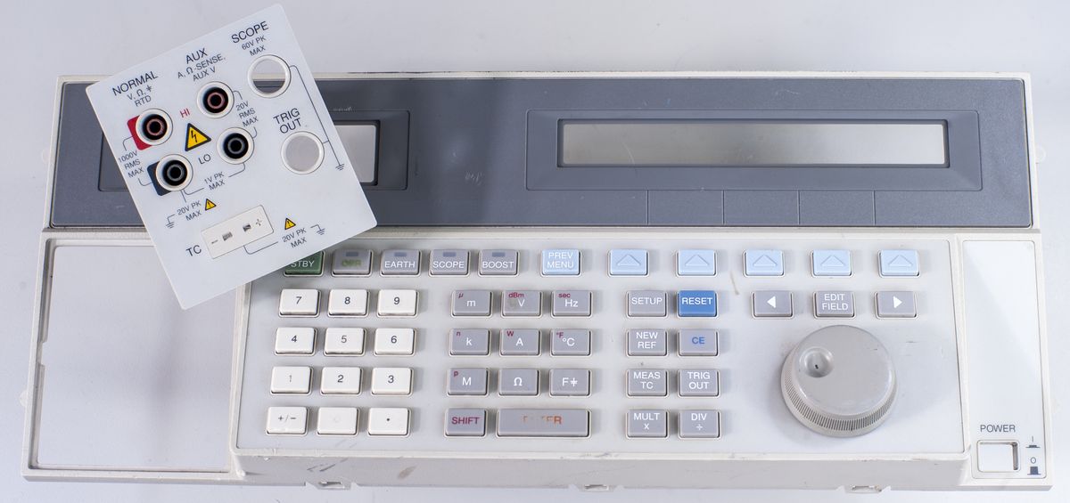
5500A series using shrounded low-thermal banana jacks and whole terminal frame is detachable. Higher performance 5520A/5522A calibrators also use 5-way low-thermal binding posts. However 5700 series blocks are part of the whole plastic front panel.
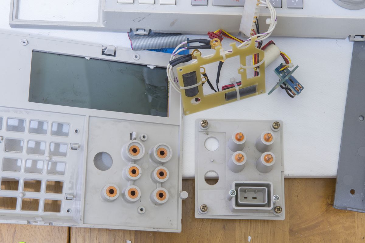
Image 31: Comparison between Fluke 5720A (left) and Fluke 5500A (right) terminals
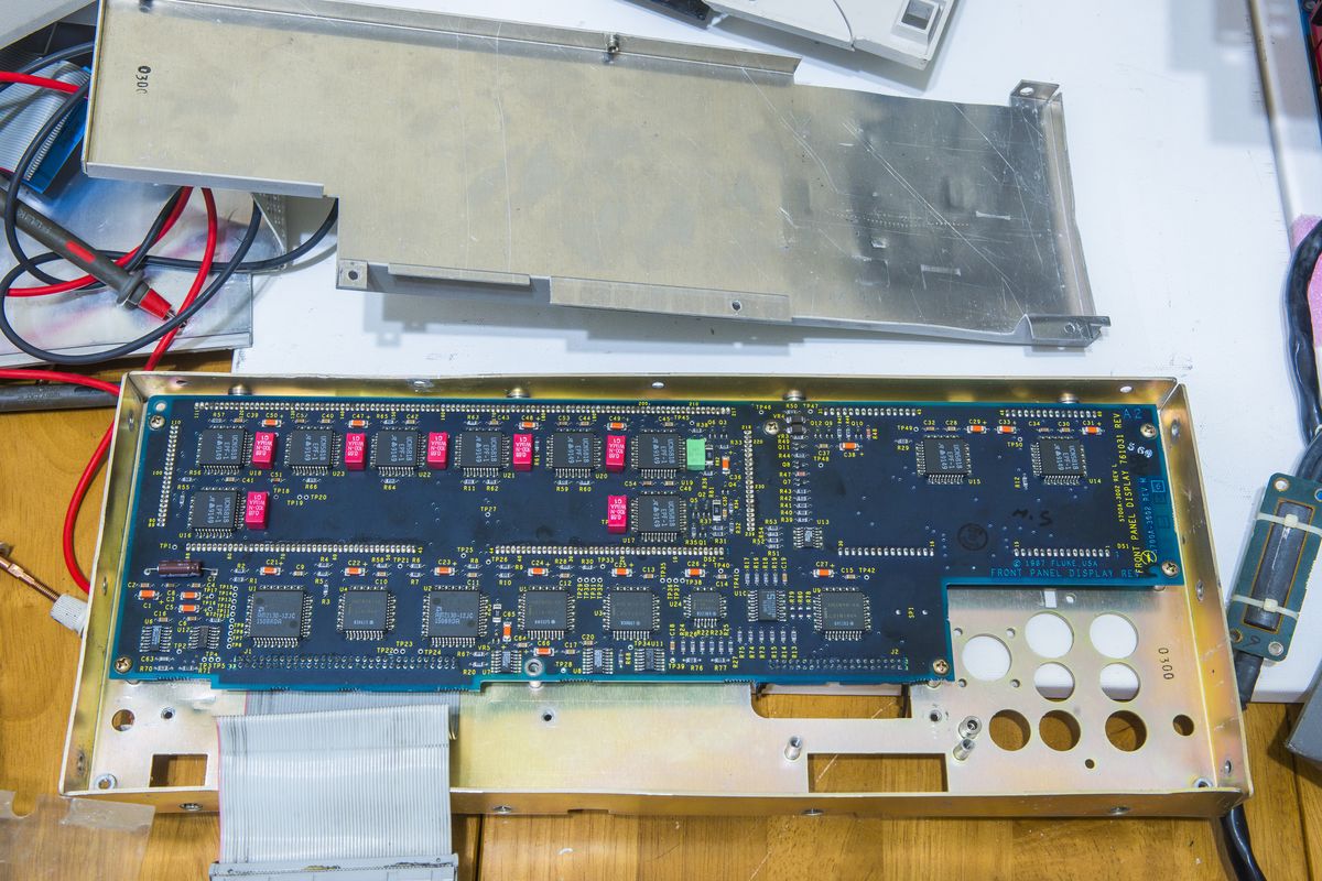
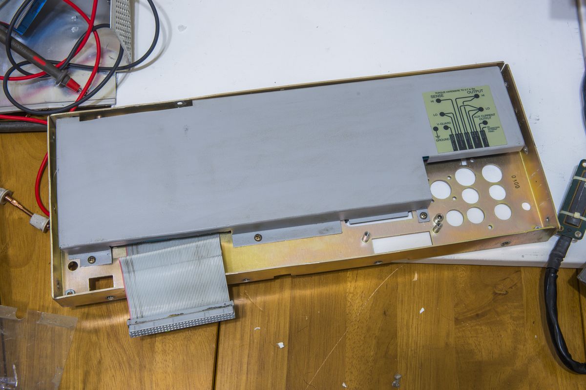
A2 PCBA with VFD glass display also fully shielded from both front and rear sides to reduce amount of noise radiated into sensitive analog signals in calibrator.
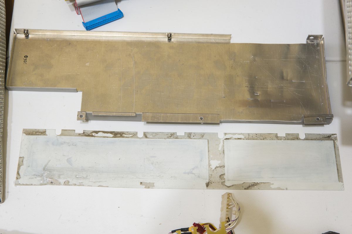
Image 32: Front panel display board EMI shield and transparent conductive display front shield
Film sheet that originally stick between VFD glass and front panel plastic is conductive. It’s some sort of (ITO?) RFI/EMI shield mylar, to reduce radiated noise from high-voltage VFD to outside of calibrator.
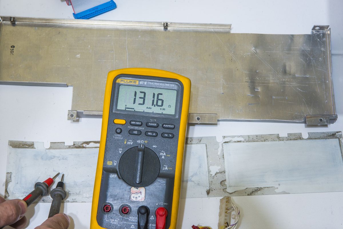
Image 33: Transparent film that glued in front of VFD is indeed conductive
Put 5700A VFD board in…
Some quick tests with reassembled panel
Scary it may look, we worry no more. Nearest hardware store with hammer and anvils will be at our service to bring this thing back to beauty in no time. No time here meant multiple evenings during 2 weeks of hammerring, drilling, riveting and swearing.
Now I’d like to make a stop on each PCBA, as we went thru the assembly process.
Main Fluke power transformer
First part to go into the reused chassis is frame with custom Fluke transformer, assembly A22.
Design of the power source with low noise performance for the precision instrument like calibrator dictate use of the linear power transformer. In high-performance calibrator product like this we care less about power efficiency of the unit, but want lowest isolated noise possible on the power rails that feed all analog circuits. 5700A power requirements are no simple thing, with many different isolated rails, with voltage levels from usual +/-5V to high-voltage +/-385V rails and high-current sections to provide enough juice for high-current PA/HV assemblies.
Also because end-to-end guarding and shielding is important, such transformer have separated sections with own shields and guard layers, to reduce coupling and parasitic leakage between unrelated sections. In simple words, this mean there is no off shelf transformer that can fit the bill here.
Frame that holds carefully fully-shielded toroid transformer assembly is heavy-duty steel, also acting as structural backbone to keep everything steady and protected from mechanical abuse.Since thermal management is also very important for calibrator electrical performance Fluke carefully designed chassis and location of all assemblies to allow correct airflow. Two 92mm x 92mm fans located by each side of the transformer get cool air intake from outguard section and rear vent and blow thru high-voltage/high-current and PSU modules at the rear less thermally sensitive wideband/switch matrix/current assemblies in front section. Most important A9/A10/A11/A12 boards are located behind transformer in low airflow zone avoiding direct drafts.
The most sensitive circuits and parts are further protected by local ovens and plastic covers, which we will in detail in related PCBA module chapters below.
Mainboards A3 and A4
Now that we have the chassis with transformer installed, time to start installing boards, with backplane PCBAs first. These boards, A3 and A4 handle signal and power interconnect for all assemblies together. These are two large thick 6-layer PCBA’s, with DIN-type 64-position double-row connectors. These boards also have physical layer of the optical VersaLink isolated interface link between floating “in-guard” section of the calibrator and earth-referenced “out-guard” section with CPU board, front panel display/keypad and I/O interface rear-board. Very similar interface we also saw before in HP/Agilent/Keysight 3458A 8½-digit DMM. Interesting similarity, given same years of development and market introduction in 1989-1990 for both 3458A and 5700A series.
Overview of A19 In-guard Power Supply PSU PCBA
Overview of A20 Processor board
Overview of A21 Rear interface and expansion board
Modularity and 5700A/5720A flexible diagnostics
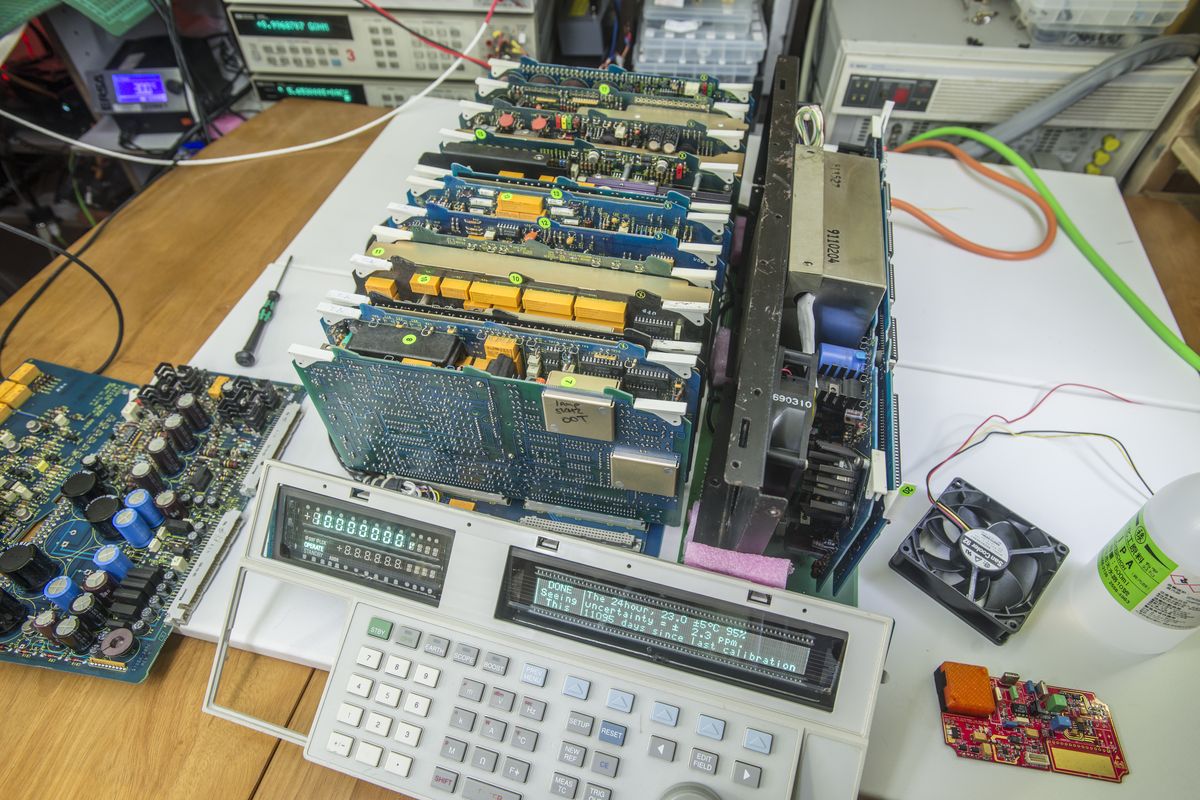
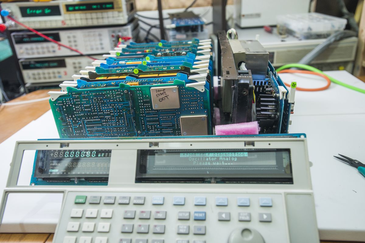
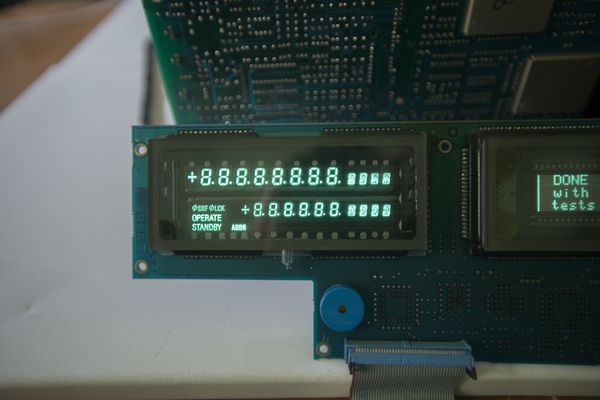
Fluke designers kept everything very modular, relatively easy to troubleshoot and follow. Many of the local functions are contained within one PCBA/module, allowing great deal of per-module repair or diagnostics. Self-test procedure is also very elaborate and runs about 20 minutes to perform hundreds of test and point measurements to provide you comprehensive diagnostics. Most of the circuitry is tested and many faults can be detected just from the self-test messages. This is great help for the Hulk project here, otherwise without having “spare” working 5700A to make “reference” measurements it would be much harder to diagnost and correctly determine faulty conditions in many mixed cases.
Wise approach here is to test minimum amount of modules/boards first , to ensure voltage regulation/power supplies correct operation and all digital control/interfacing work. Experimentally we determined that to provide valid hardware configurations for functionality checks.
| Config, Hardware setup | Modules installed/used | Provided functions |
|---|---|---|
| A, Inguard digital + power test | A3+A4 + A19+A20 + A1+A2 Front panel + A21 | Unit boots firmware, display VFD, hang on error “Guard crossing” |
| B, Inguard + outguard power test | Same as A + A18 PCBA | Unit hangs on “Guard crossing”, but now can check outguard power pre-regulator / filter |
| C, Outguard power test, cross-guard interface | Same as B + A17 PCBA | Unit boots, allow to navigate menus, but no any outputs/functions |
| D, DCV function test | Same as C + A8 and A11 PCBA | Unit boots, allow to output 220mV,2.2V,11/22V DC Voltage |
| E, DCV+Resistance function test | Save as D + A7,A9,A10 PCBA | Unit boots, adds Resistance and DC Current 220 µA – 220 mA |
| F, ACV function test | Same as E + A12,A13 PCBA | Unit boots, adds ACV and ACI functions, except 2.2A and 1kV ranges, ACAL can be finished |
| G, PA test | Same as F + A16 PCBA | Unit boots, adds 220 VDC and 220 VAC range, ACAL can be finished |
| H, HV/HC test | Same as G + A14,A15 PCBA | Base configuration, adds 2.2A and 1kV ranges. ACAL fully enabled |
| K, Wideband option | K + Add optional A5+A6 PCBA | Full configuration with 2.2mV – 3.5V 30MHz Wideband option |
| W, Boosted option | Connect 5725A to expansion port | Enables 11A DCI and ACI, extends V/F limits for 1kVAC range |
Configurations in bold letters allow complete self-test and artifact calibration procedures to be completed without errors.
Overview of A18 Filter/PA PSU PCBA
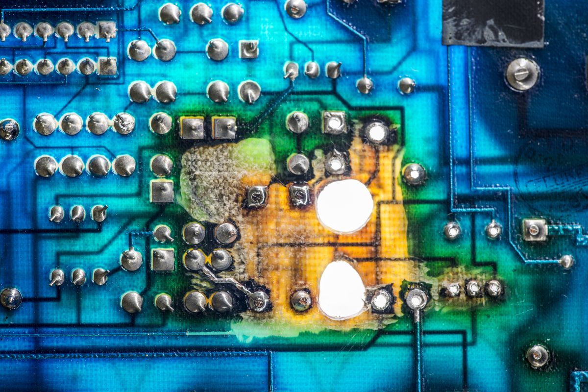
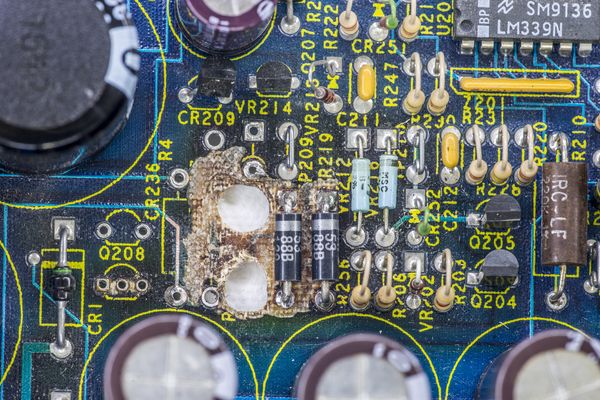
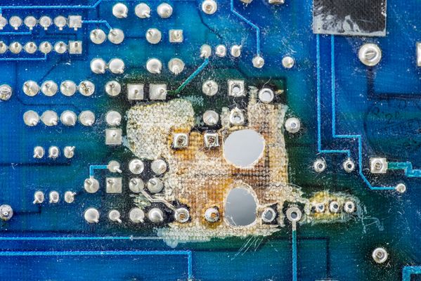
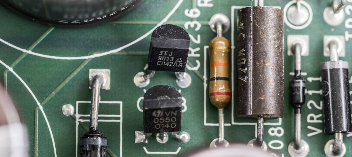
At this point A18 inguard PSU/filter board can be tested and repaired. This board was acquired broken, with typical issue of these old board. There are carbon 220 KΩ 3W resistors used in high-voltage PA regulator stage. These resistors do not survive burden of the years, and in many old boards they fail to low resistance, get too hot, and cook everything around due to excessive currents and voltages.
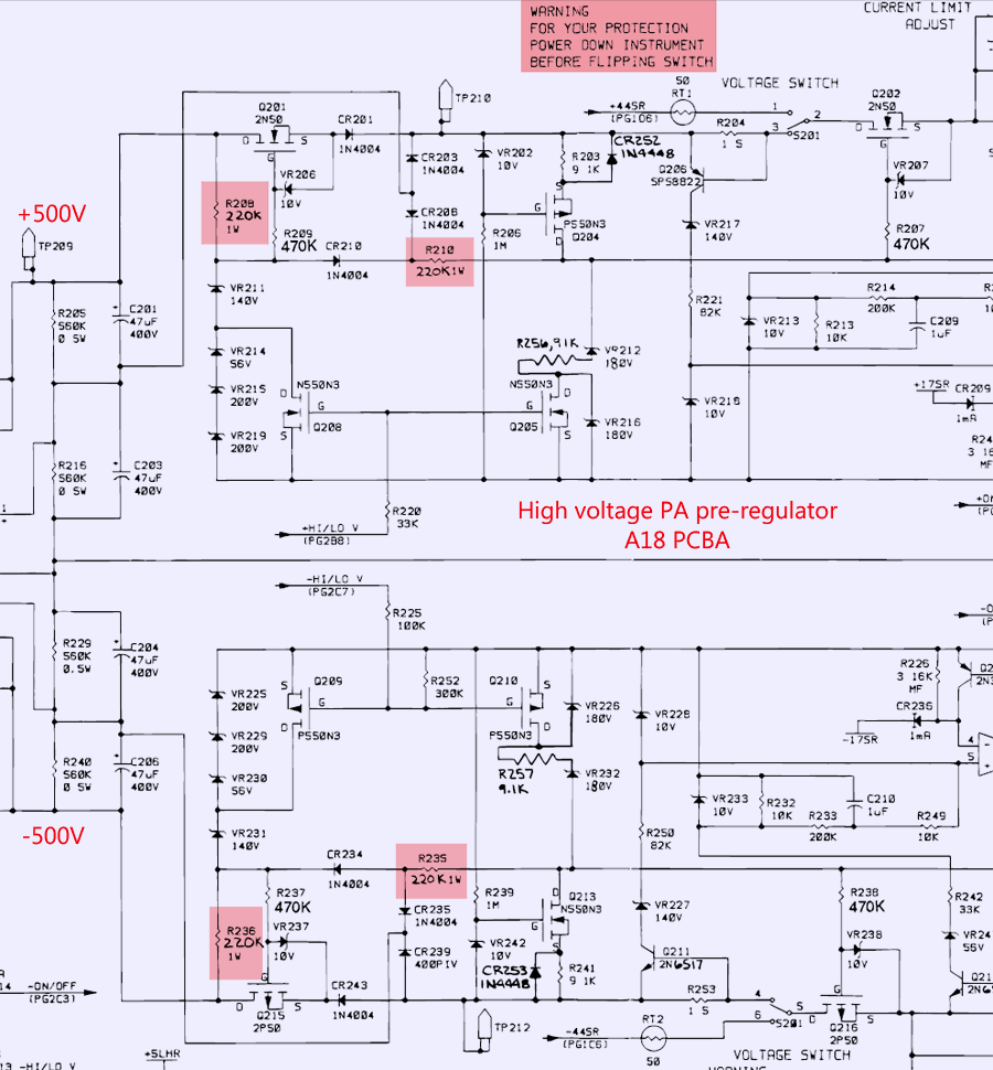
If one to service old 57XX unit, I would go and check these resistors first thing, before even power on. If not, board will be burned and result will present itself as photos below on our A18.
This was condition already after most of charcoal material removed by milling out affected areas. A18 PCBA is 4-layer, so internal broken connections will have to be repaired with jump-wires and patches.
Does not look very pretty, but it will do.
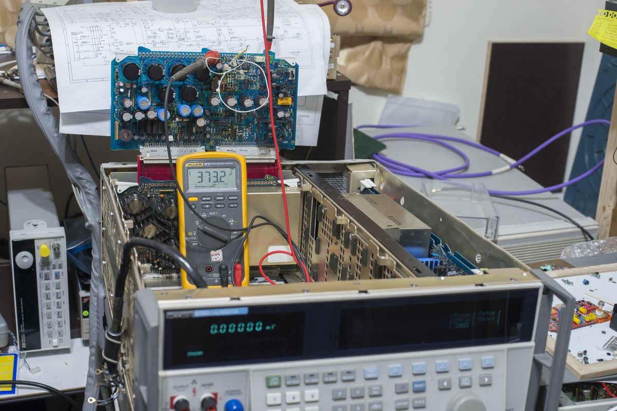
Correct 475 VDC output on TP210 measured, and +373V on output of the PA as expected.
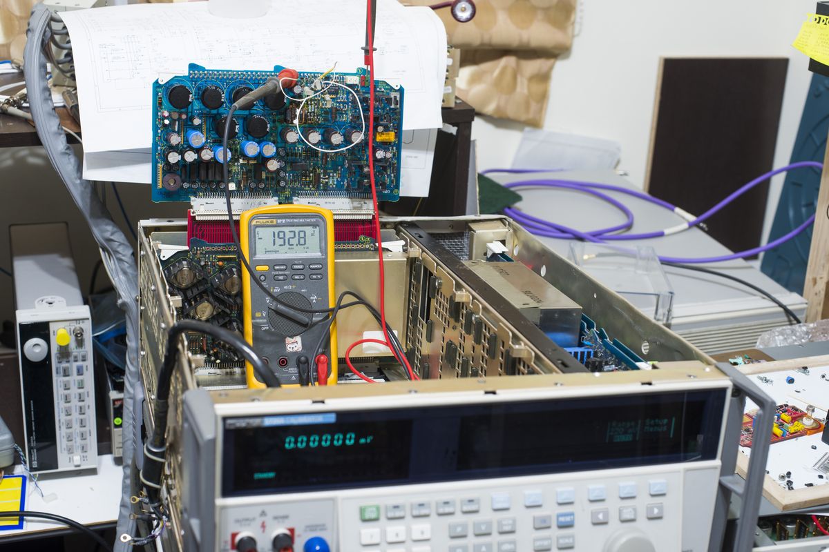
Correct -190 VDC output on TP204 measured, as expected for negative PA rail.
The Filter assembly receives various ac inputs from the main power transformer and provides unregulated dc to the Regulator/Guard Crossing assembly (A17), and regulated dc supplies +5FR1, -18FR1, and -5FR2 to the DAC assembly.
The unregulated supplies are listed in Table 2-8 and the regulated supplies are listed in Table 2-9.
44 S COM and 17 S COM are tied together on the Regulator/Guard Crossing assembly (A17).
Unregulated supplies from A18
| Name | Nominal output | Tolerance | Max ripple Vpk-pk | Rated output | Test point |
|---|---|---|---|---|---|
| +15 OSCR | 27V | ±8V | 2V | 200 mA | TP2 |
| -15 OSCR | 27V | ±8V | 2V | 200 mA | TP5 |
| OSC COM | RETURN | TP4 | |||
| +5 LHR | 12V | ±4V | 3V | 3.5A | TP1 |
| -5 LHR | 12V | ±4V | 2V | 400 mA | TP6 |
| LH COM | RETURN | TP3 | |||
| +44 SR | 60V | ±15V | 3V | 155 mA | TP7 |
| -44 SR | 60V | ±15V | 3V | 460 mA | TP9 |
| 44 S COM* | TP22 | ||||
| +17 SR | 27V | ±8V | 3V | 1.3A | TP10 |
| -17 SR | 27V | ±8V | 3V | 1.3A | TP14 |
| 17 S COM* | RETURN | TP12 | |||
| +5 FR1R | 12V | ±4V | 2V | 400 mA | TP17 |
| -18 FR1R | 27V | ±8V | 2V | 50 mA | TP20 |
| FR1 COM | RETURN | TP19 | |||
| +30 FR1R | 50V | ±15V | 3V | 85 mA | TP15 |
| FR1R COM | RETURN | TP16 | |||
| +30 FR2R | RETURN | ±15V | 3V | 85 mA | TP8 |
| FR2 COM | TP11 |
Regulated supplies from A18
| Name | Nominal output | Tolerance | Current limit | Rated output | Test point |
|---|---|---|---|---|---|
| -5 FR2 | -5V | ±0.3V | 0.15A | 0.03A | TP13 |
| FR2 COM | RETURN | TP11 | |||
| +5 FR1 | +5V | ±0.3V | 2A | 0.1A | TP18 |
| -18 FR1 | -18V | ±0.9V | 2A | 0.05A | TP21 |
| FR1 COM | RETURN | TP19 |
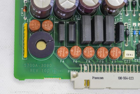
Overview of A18 Filter/PA PSU PCBA from Fluke 5720A MFC
A15 – High-voltage/High-current assembly
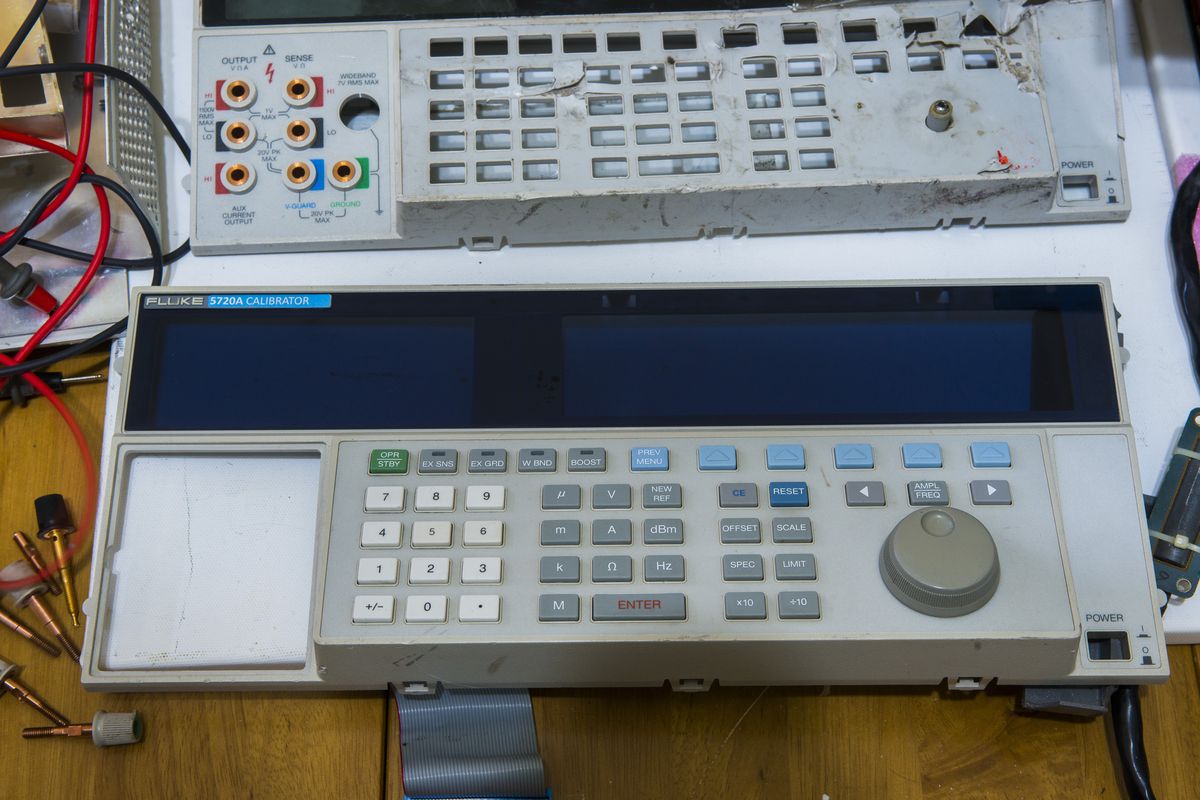
Front panel repairs
Condition of the front panel before:
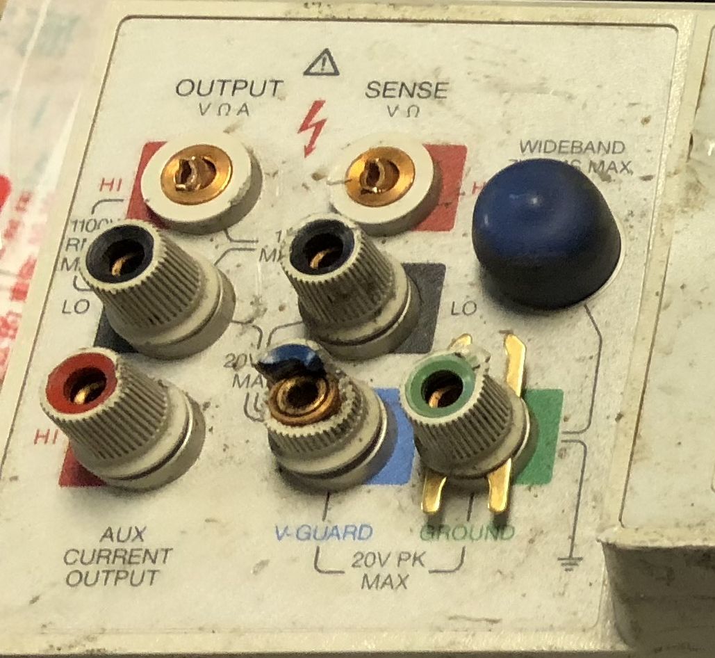
Condition after on my Fluke 5500A frame.
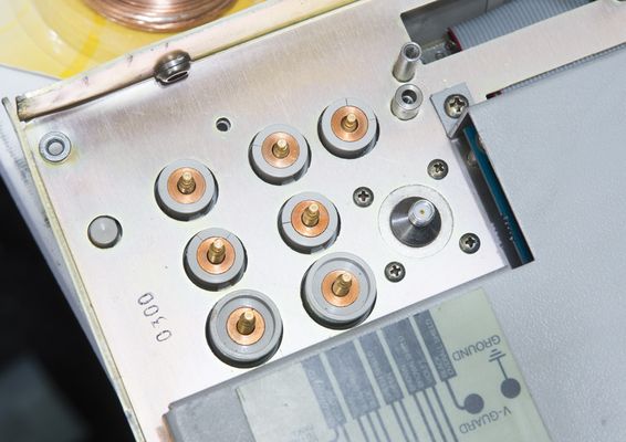
I had to file 0.3mm for key on the rods to make them fit the original Fluke base. Other the cap plastic color, rest of the LowThermal connector is identical.
After few weeks of playing with hammer and drill, we got things to align.
Rear right corner still need attention, but at least at this point boards can be fitted and mount holes are align together. Most of them, at least.
A8 assembly
Fix for 220mV gain S4 calibration error
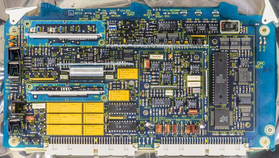
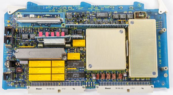
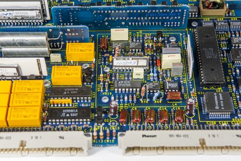
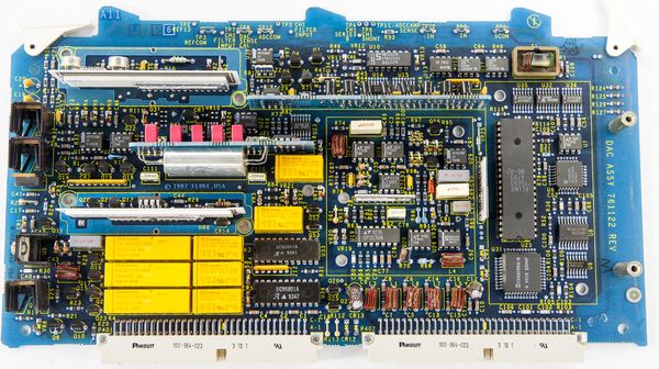
Overview of A11 DAC PCBA from Fluke 5700A MFC
Fluke 5700A Service manual has schematics and short description of DC reference and DAC module operation theory, so it’s worth to refresh memory reading related sections to get familiar with DAC module design.
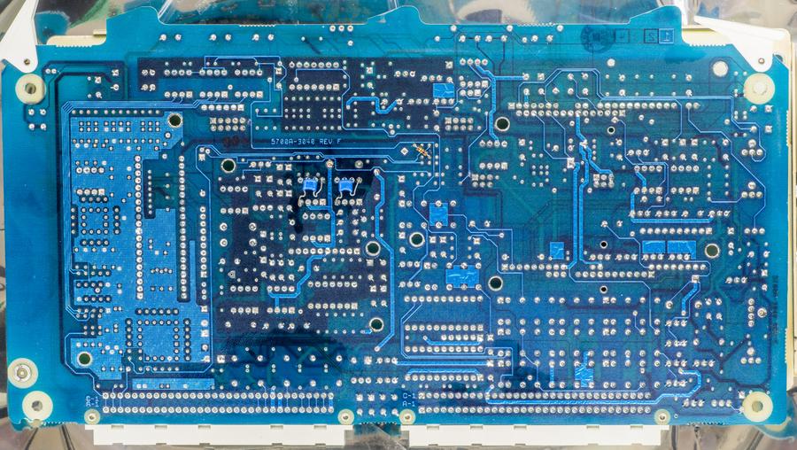
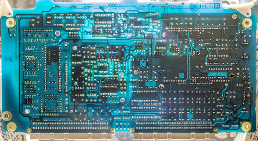
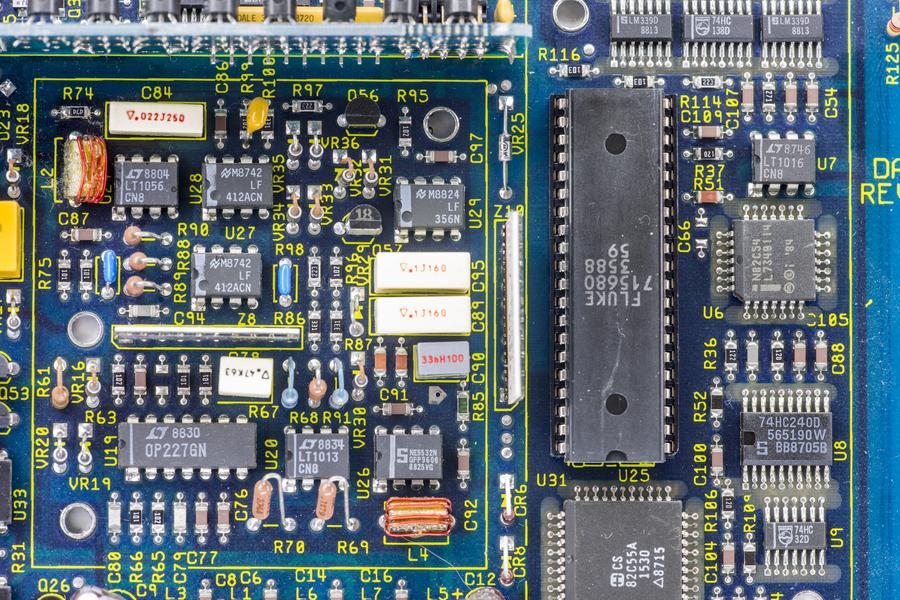
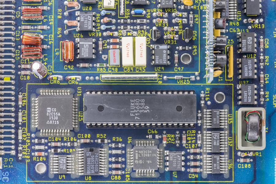
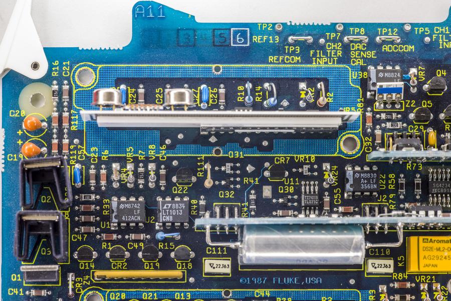
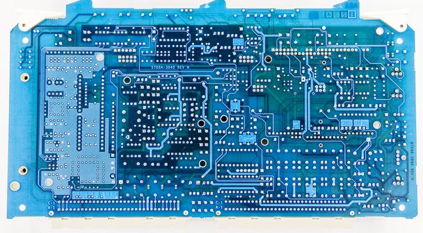
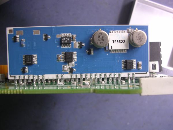
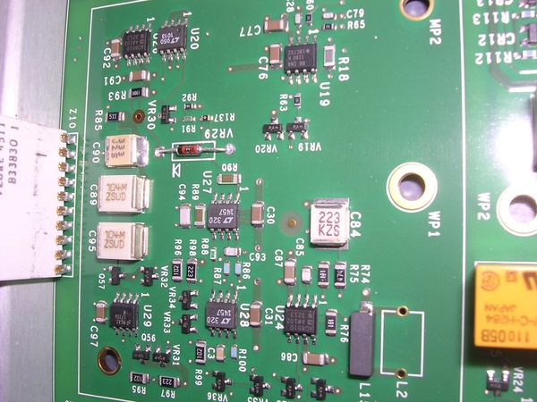
PCB with blue soldermask is 6-layer FR4, with most of the routing buried on inner layers. There are only few ground mesh fill polygons, around digital components, such as MCU, clock generator and ADC. Stripline routing might serve two purposes here – act as additional protection sensitive analog traces from environment and surface contamination. Book Basic Linear Design from Analog Devices covers some of ideas how PCB leakage and bad layout could introduce errors and issues in sensitive analog design.
DAC assembly provide adjustable stable DC voltage output, from 0 to +11VDC and features multiple subassembly units.
- DC Reference hybrid (HR5)
- DC Amplifier hybrid (HR6)
- DAC Filter SIP
- DAC mainboard
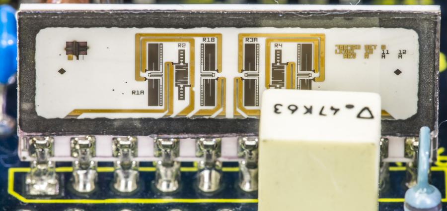
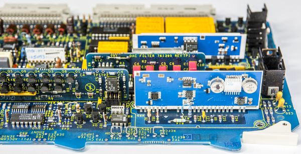
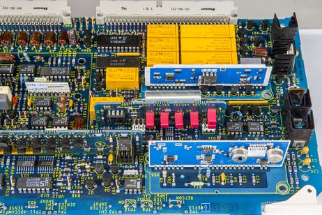
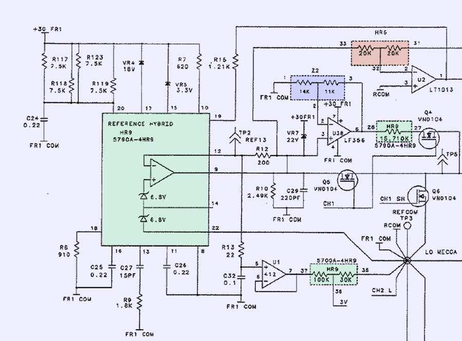
Fluke used PWM-controlled method to generate adjustable voltages. There are also few auxiliary support circuits on-board, such as sense-current cancellation block, linearity tune control, negative offset control. Block diagram below on Image 4 can help to understand overall function of circuitry on A11 DAC PCBA.
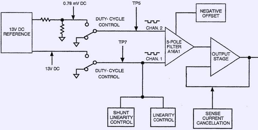
Output DC voltage is generated by 5-pole discrete filter, which has two precision square waves of different amplitude as the input. First input channel of the filter is CH1, and it’s amplitude is from 0V to reference voltage, which is around +13 VDC. This is coarse adjustment channel. Second CH2 channel is operated similar way but goes up only to attenuated reference voltage at +0.78 mVDC. This is fine tune adjustment channel. Filter is designed as LPF with bandwidth 30 Hz, and input square wave frequency is 190 Hz. So the output is clean and filtered DC voltage, derived from controlled PWM CH1 + CH2.
Filter output does not have capability to drive large currents, so output stage on separate ceramic hybrid takes filter output and provide driving capability for DAC output. Hence after all, circuit output voltage can be predicted and calculated by simple formula:
VOUT = DutyCH1 * VREF13V + DutyCH2 * VREF0.00078V
Here’s realtime example to try some values to generate precise 10V:
Use of this combined PWM scheme allows us to have efficient way to generate arbitrary voltage levels without use of very expensive resistor networks and expensive complex multi-bit DAC ICs. PWM duty cycle resolution of PWM generator used in Fluke calibrator is 0.0024%, which provides resolution of CH1 = 309 µV/bit and CH2 = 18.5nV/bit. PWM signal also electrically isolated by optocouplers.
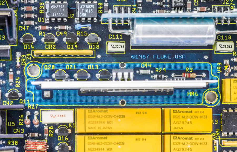
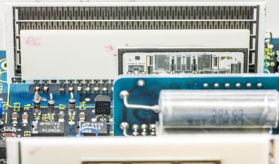
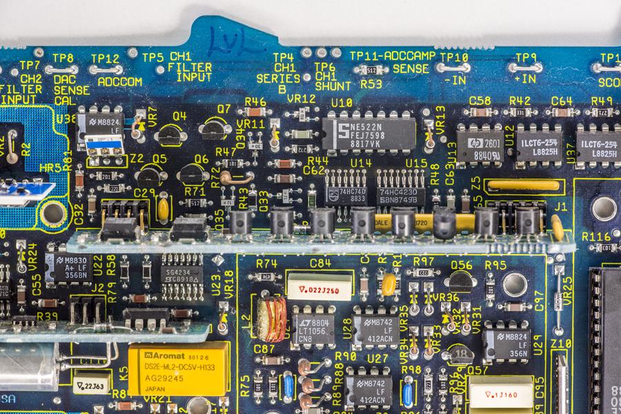
Dark color covers around HR5 and HR6 hybrid assembly are not metal, but metallized plastic. Main purpose of these covers is to prevent stray airflow around reference circuity and DAC chopper amplifier. This is important due to parasitic thermocouple EMF-generation effect present with any thermal gradient within the board. Also since hybrids are actively heated, enclosure helps with thermal stability of inner thermostat area. Don’t forget, Fluke 5700A dissipate plenty of power during operation and has two large fans to provide airflow around PAs and high-power components and boards.
ADC section and PWM generator/digital controller are separately enclosed in metal cage shield on the top side. This serve dual purpose, to keep generated RFI/EMI enclosed and localized and to provide additional shielding from external fields. These shields are grounded to module power ground plane.
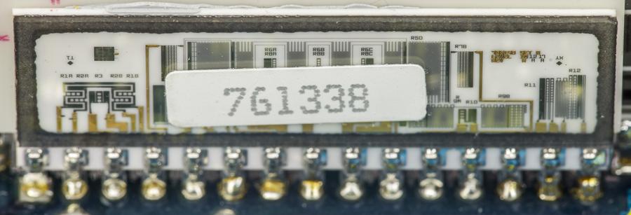
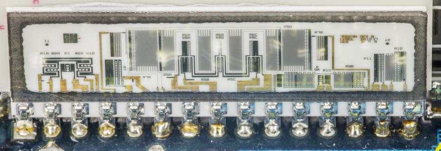
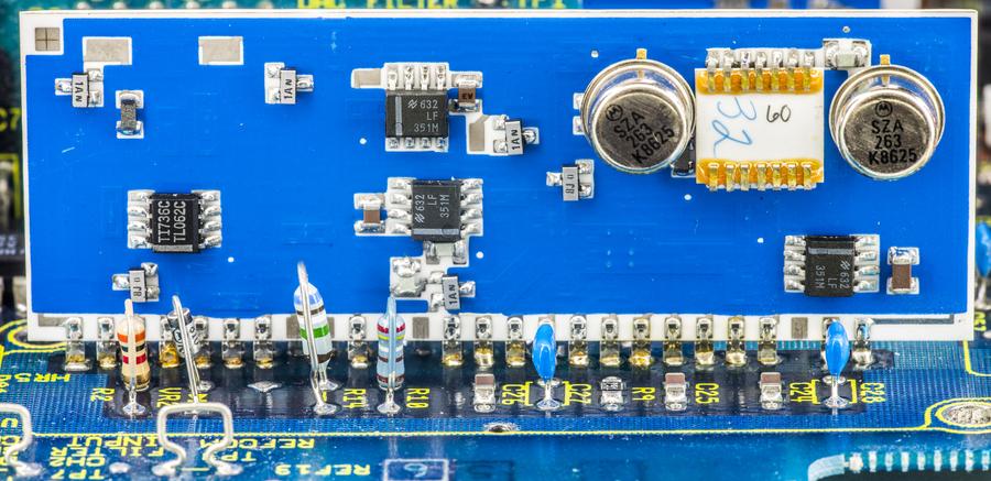
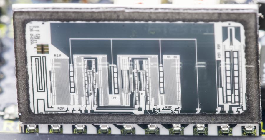
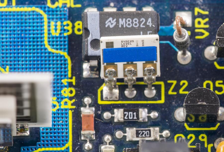
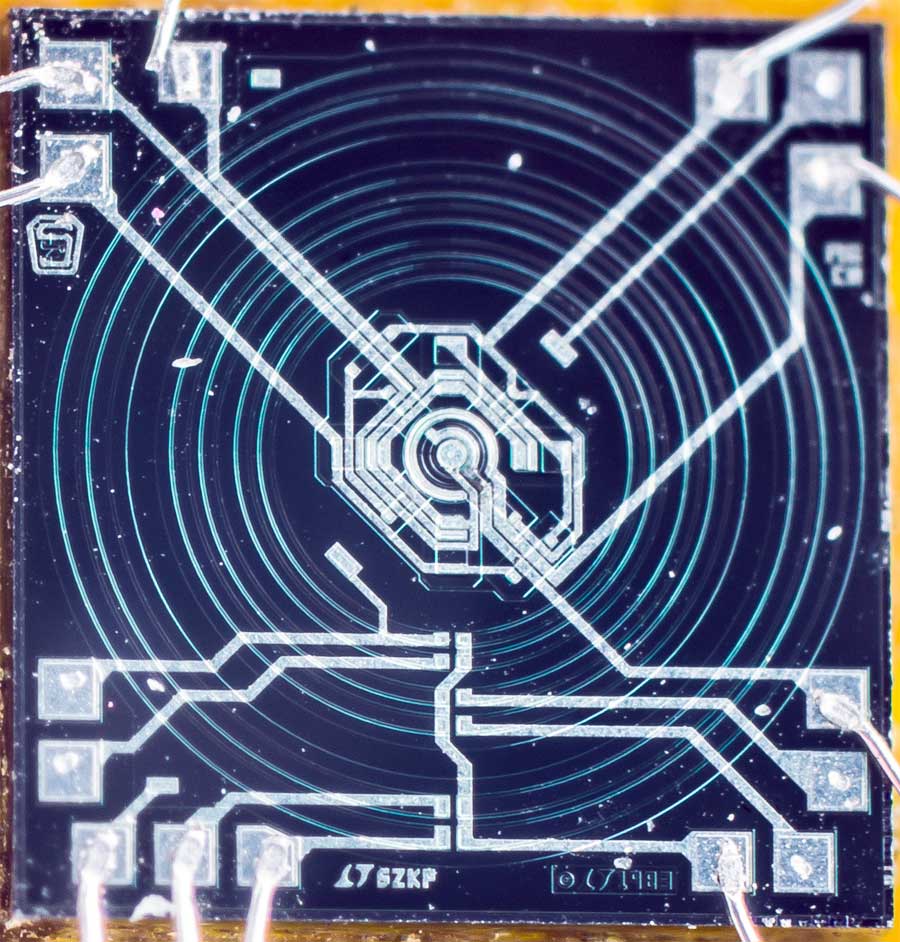
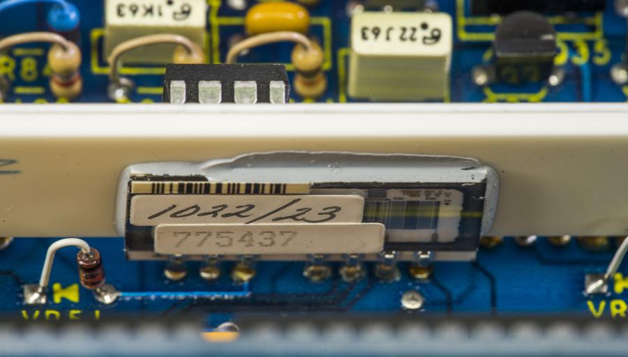
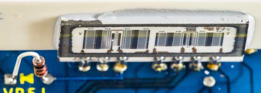
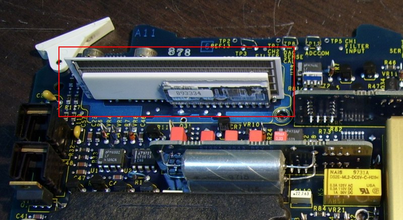
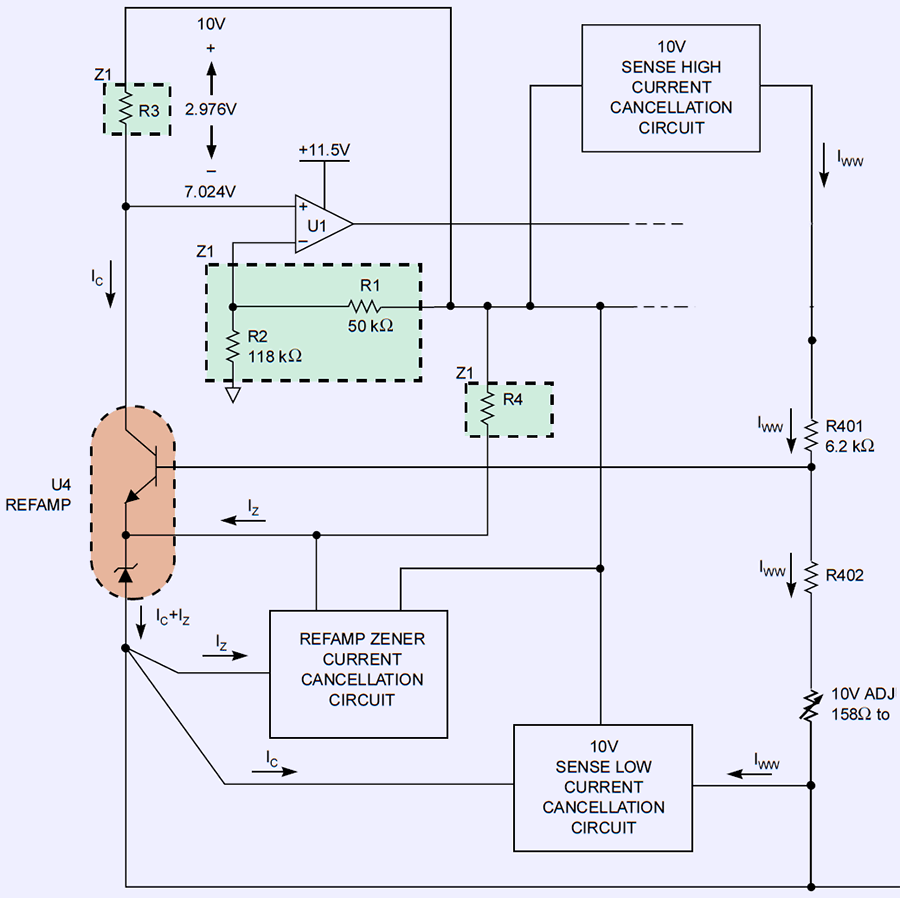
Main DC reference hybrid is built using sandwich of ceramic substrates. Main thin substrate has two Ref-Amp, hybrid resistor network, few opamps, temperature resistors and circuit tracks. Back side of HR5 has large area 27 Ω resistor acting as a heater. Then there is glued spacer to act as a heat-spreader and coupled to it hermetic hybrid resistor with clear quartz window for laser trim access.
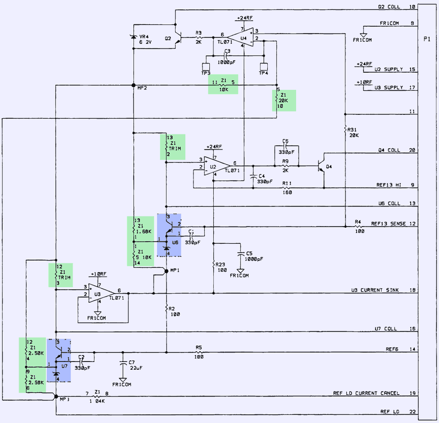
All parts except Ref-Amps, which as Motorola SZA263 are SMT-mount. Two Ref-amps are used to provide higher +13 VDC (6.5 + 6.5) reference level to further reduce amount of noise and improve stability of the DAC. Excellent temperature coefficient of used Ref-Amps is achieved by using stable collector bias current of their transistors provided from stable thin-film resistor hybrid between Ref-Amps. This design allow to have very small output voltage impact from circuit component errors, so it’s output stability directed almost entirely from Motorola SZA263 performance.
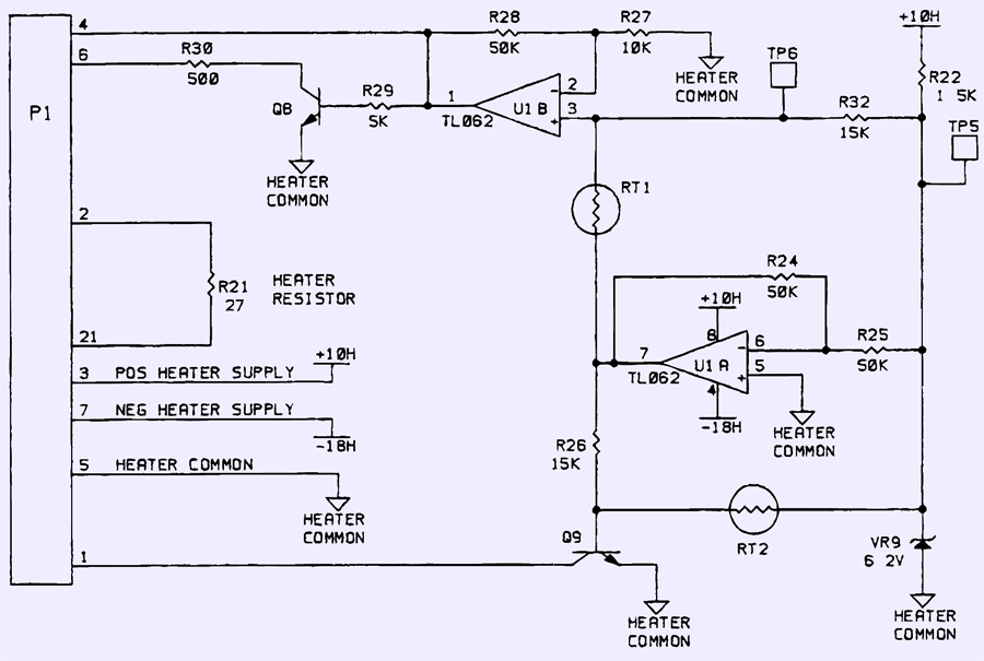
To prevent output drift with respect to ambient temperature whole assembly heated to constant +62 °C by external circuit block on main A11 PCBA. Temperature feedback element is thermistor RT1, located right near the Ref-Amp packages. As ceramic is a good thermal conductor, any change in temperature of hybrid will drive correction signal to Q2 on main board and have circuit adjust power to 27 Ω film resistor to adjust temperature back to set-point. There is also thermal runaway protection, implemented with second thermistor RT2, which activates Q9 to bypass base current of Q1 to avoid overheating. This protection kicks in once substrate temperature reaches +67 °C, and normally should be never used.
Interesting to note that improved Fluke 5720A also has changes in this HR5 DC reference hybrid, as we can see thanks to lymex from bbs.38hot.net chinese forums, who released photo of HR5 used in Fluke 5720A A11:
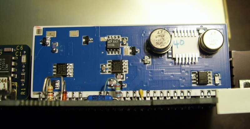
Pair of Motorola SZA263 chips replaced by Linear LTFLU-1ACH, and LF351 opamps are replaced with Linear LT1006 and TL071C.
Hybrid laser-trimmed resistor network is smaller and have different configuration as well.
Very similar dual Ref-Amp assembly used also in Fluke’s AC measurement standard, Model 5790A on A16 DAC board.
Bit simpler version with only one Ref-Amp is used in Fluke 5500A/5520A and system calibrator 57LFC. There is thermal control over ref-amp assembly in these calibrators either. So as a result DCV performance of these calibrators is “only” 11 ppm annual, with daily stability 2 ppm. Fluke 5700A has 8 ppm annual, and updated 5720A/5730A are half of that, 4 ppm.
Of course if better temperature stability is achieved with removal of all airflow, actual Ref-Amp can provide much better performance. This is proven by ± 2.0 ppm/year and 0.3 ppm/day specifications and actual performance of double-oven Fluke 732B reference assembly.
Let’s take a brief look on 732B reference assembly block diagram:
Power supply requirements of A11 PCBA
In this section we determine what requirement are to get A11 PCBA operational and working, without calibrator mainframe itself.
What is the Ref-Amp?
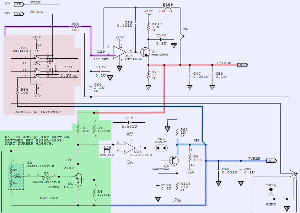
Ref-Amp consists of an NPN transistor in series with a zener diode. When biased properly, the combination has a extremely low temperature coefficient. The reference voltage that the can vary from +6.5 VDC to +7 VDC, depends on actual production bath. Also since both zener and transistor are located on same substrate and enclosed in hermetic package, they are tightly thermally coupled and protected from ambient humidity. This allows to improve stability over long time spans.
There are two well-known examples of this device family, Ref-Amps used by Fluke in high-end instrumentation equipment. These are Motorola SZA263 and Linear LTFLU-1H/LTFLU-1AH.
The Motorola SZA263 is a “Ref-Amp” that was made by Motorola, and later discontinued after getting out of high-volume semiconductor business. This forced Fluke to find a partner to design a replacement for the obsolete SZA263, as Motorola would not sell the design files and masks of original design. Linear Technology was happy to help big customer like Fluke with the design, and that’s how LTFLU-1AH Ref-Amp emerged. It’s pin-2-pin and function compatible with the original SZA263, but the LTFLU-1AH use bit aluminum alloy for the interconnects, which is not the same one Motorola used. This rendered in different long-term stability, visible by positive drift over time on SZA263, but negative in LTFLU-1AH (same as LTZ1000/LTZ1000A and the LMx99 ICs).
If you have a bank of 4 × 732A’s and a bank 4 x recent 732B’s that you get calibrated once a year, you will clearly see these drift patterns. Care need to be taken though, as early batches of Fluke 732B were still using left-over SZA263’s, but later all production 732B were updated to LTFLU-1AH.
Main differences summary between the SZA263/LTFLU-1AH IC and the market-available Linear LTZ1000 are:
- Different package. LTFLU-1AH is 4-pin hermetic can, the LTZ1000 in an 8-pin TO-99. They are far from drop-in compatible.
- SZA263/LTFLU-1AH has the transistor for temperature compensation in series with the zener, not parallel as LTZ1000 design.
- Due to different manufacturing process, Motorola SZA263 have positive long-term drift, while Linear LTFLU-1AH has negative long-term drift.
- Opposite to LTZ1000A, there is no on-die heater in SZA263/LTFLU-1AH
- SZA263/LTFLU-1AH require much more time (vs LTZ1000 design) and care for support resistor matching and tempco testing
Last item is due to different tempco compensation transistor arrangement in SZA263/LTFLU-1AH circuit, which needs more attention for temperature and current compensation than LTZ1000 circuits. LTZ1000 design is fine even with standard datasheet reference schematics, without any analog black magic or voodoo.
All this above of course less a problem than zero availability of LTFLU-1AH, as Fluke have exclusive rights for this design and chip, and Linear is not allowed to sell Ref-Amp on open market. So Motorola SZA263/Linear LTFLU-1AH are less friendly solution to implement a stable DC reference, as even if you get LTFLU-1AH chip, lot of time and money for resistor matching and temperature testing is required.
Die photos of LTFLU-1AH and other references
LTFLU-1AH
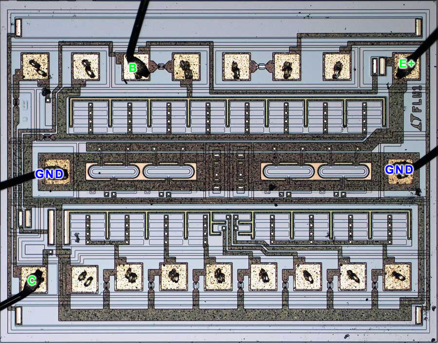
LTFLU-1CH die photo. Courtesy branadic (Dipl.-Ing. A. Bülau) from the EEVBlog
On the die photo we can see much more complex design than just diode and transistor.
LTZ1000ACH
Here’s die photograph of Linear LTZ1000ACH chip:
LM399
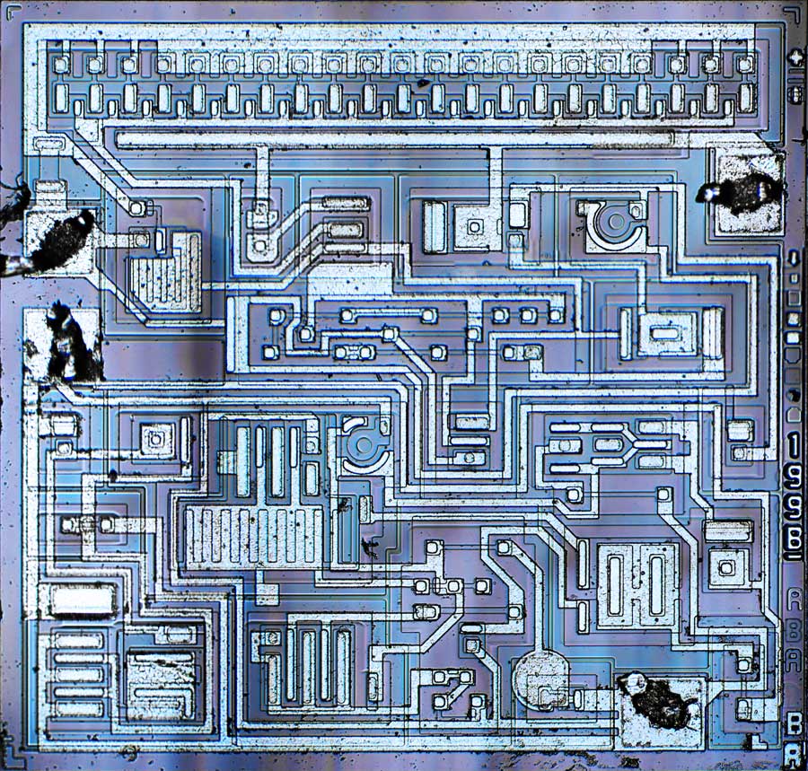
National Semi LM399 die photo. Courtesy branadic (Dipl.-Ing. A. Bülau) from the EEVBlog
LTC6655
Instruments list using Ref-Amp
Known instruments to implement SZA263/LTFLU-1AH as primary DC reference:
- Fluke 341A DC Voltage Calibrator
- Fluke 343A DC Voltage Calibrator
- Fluke 515 Portable calibrator
- Philips PM2530 7½-digit DMM
- Fluke 8840A DMM
- Fluke 8842A DMM
- Fluke 8508A DMM
- Fluke 8588 and 8558A DMM
- Fluke 731B DC Voltage Standard
- Fluke 732A DC Voltage Standard
- Fluke 732B DC Voltage Standard
- Fluke 732C DC Voltage Standard
- Fluke 5440B DC calibrator
- Fluke 5500A Multi-function calibrator
- Fluke 5520A Multi-function calibrator
- Fluke 5522A Multi-function calibrator
- Fluke 5800A Oscilloscope calibrator
- Fluke 5820A Oscilloscope calibrator
- Fluke 5540A calibrator
- Fluke 5550A calibrator
- Fluke 5560A calibrator
- Fluke 57LFC System Calibrator
- Fluke 5700A Multi-function calibrator
- Fluke 5720A Multi-function calibrator
- Fluke 5730A Multi-function calibrator
- Fluke 5790A AC Measurement standard
- Fluke 5790B AC Measurement standard
- Keithley DMM7510 7½-digit multimeter
There is also great thread here on EEVBlog created by lymex, revealing guts of various DC voltage standards.
Second A11 DAC PCBA from Fluke 5700A II MFC
This is newer A11 DAC assembly, perhaps from Fluke 5700A II series, as it have some additional modifications, not present on my first A11.
I’ve manage to damage chopper hybrid assembly HR06 when removing plastic cover, cracking corner a bit. This was “repaired” by adding 3 copper jump wires instead of broken connections under blue protective coating. But top and middle 400 Ω-ish segments are now not connected, so it may have unwanted thermal gradients.
This board also sports Linear LTFLU-1CH chips instead of older Motorola SZA263.
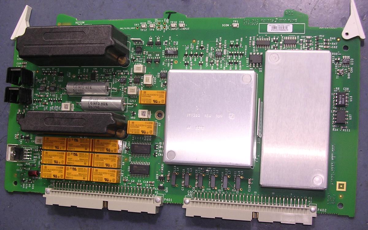
Modern Fluke 5720A/5730A REFDAC A11 module
Thanks to pipelie and his friends, we get photos of modern A11 REFDAC assembly, implemented using current SMT-mount components, except few hybrids.
Per datecodes on chips, this module manufactured around year 2011. We believe it’s the one used in all current Fluke 5730A and newer 5720A units build since 2010+.
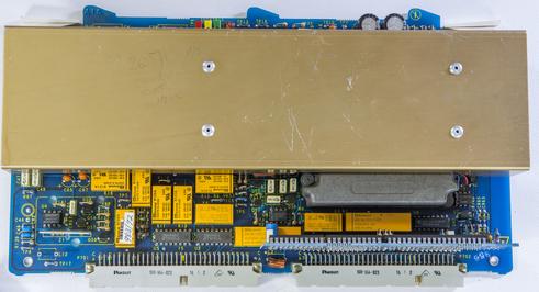
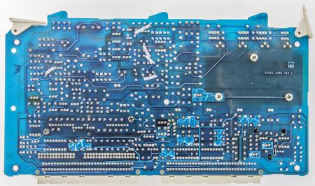
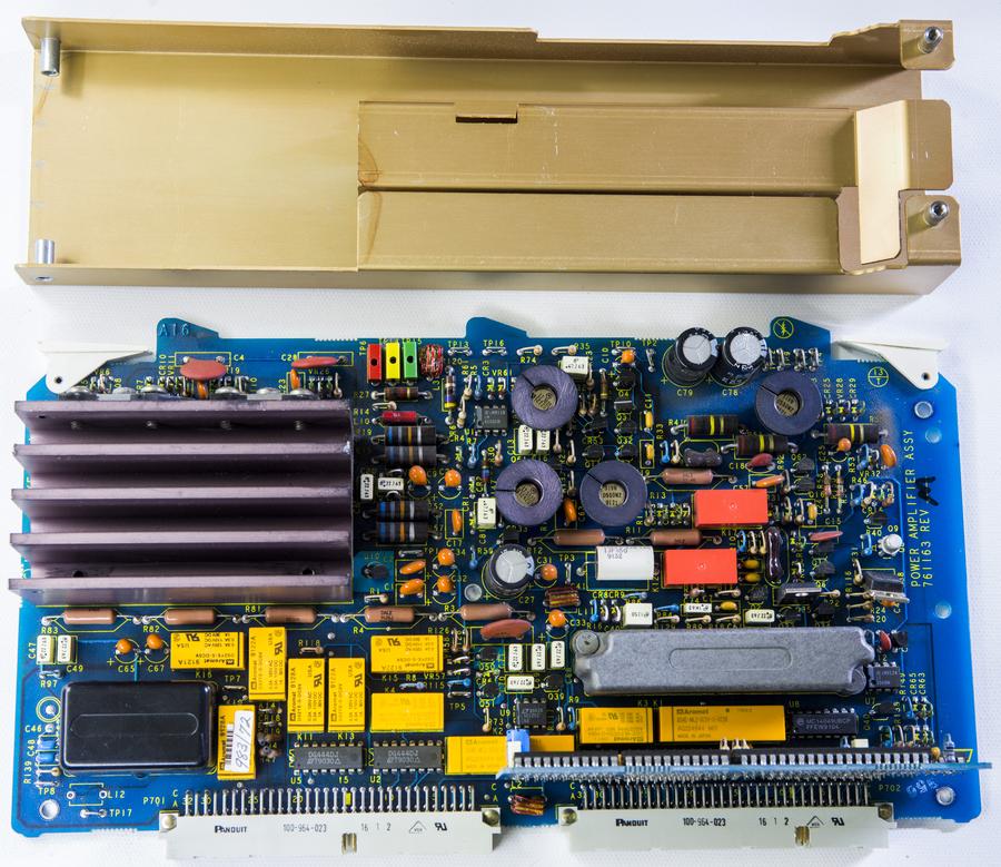
A16 – PA PCBA from Fluke 5700A MFC
The A16 PCBA PA PCB outputs DC voltages from ±22V to ±219.99999V and AC voltages from 22V to 219.99999VRMS. The frequency limit for 220V AC output is 100 kHz. Output voltage limits are derated at frequencies above 100 kHz. At 1 MHz, the maximum output voltage is 22 VRMS. The PA drives the High Voltage assemblies (A14, A15) in all high voltage and high current functions. This assembly also contains calibration circuitry that enables the internal calibration system to determine exact PA AC and DC gain, offsets and frequency response.
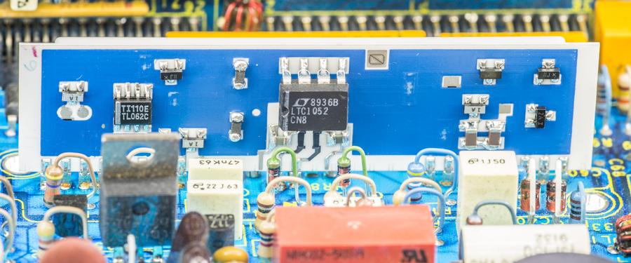
The main sections of this assembly are the input stage, mid stage, output stage, sense current cancellation circuit, the DC and AC gain calibration circuits, and the PA Digital Control SIP assembly (A16A1), which is mounted on the PA PCB vertically.
Digital control for the PA PCB is contained on the SIP assembly (A16A1) mounted at the bottom of the PA. This assembly configures the PA PCB for its various modes of operation. The heart of the Digital Control assembly is an 82C55 Programmable Peripheral Interface IC (U11) operating under software control via the guarded digital bus. This IC has three ports that generate 24 outputs. These outputs control two 5801 relay driver ICs (U10, U12), two LM339 Comparators (U13, U15) and an analog multiplexer (U14) used for diagnostics.
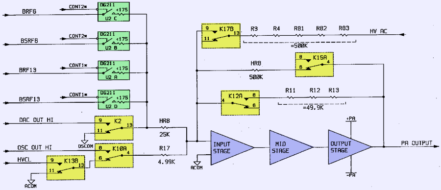
PA Common Circuitry
Common circuitry consists of the +PA and -PA supplies, input stage, mid stage, and the output stage. PA input node, gain, and feedback are different for DC and AC operation. PA gain is -20 in the DC function, determined by the ratio of resistor network bonded to the HR8 assembly (500 kΩ/25 kΩ). Gain in the AC function is -10, which is determined by the ratio resistors [(R11 + R12 + R13)/R17].
+PA and -PA Supplies
The ±PA supplies are high voltage supplies generated by the Filter/PA Supply assembly (A18). These supplies can be controlled by the Digital Control SIP assembly (A16A1) and are switched between the two modes, either ±185V or ±365V. Theory of operation for the Filter/PA Supply assembly (A18) in service manual describes how these voltages are generated and selected.
PA Input Stage
The input stage consists of a heater-controlled hybrid HR8, Linear LTC1052 opamp U7, transistor Q6, and JFET Q2. The HR8 assembly consists of an opamp mounted on a heated-substrate hybrid, with a resistor network bonded to it. Hybrid HR8 provides the input stage with excellent DC characteristics of low offset, noise and drift. The hybrid heater-control circuit (on sheet 3 of the schematic in service manual) adjusts the base voltage of Q38 to deliver the correct current to the heater resistor. This maintains the hybrid assembly at a constant temperature in spite of environmental temperature variations. Transistor Q35 protects the hybrid in case Q38 fails. Input of the hybrid opamp is protected by CR13 and CR14.
Output of the hybrid opamp is connected to the input of a faster opamp (U7), which provides additional DC gain and a higher slew rate. JFET Q2 and transistor Q6 combined with these two opamps complete the input stage. Q2 is a very low-bias-current, high-frequency JFET.
The input stage operates with low voltage supplies (±17V) whereas Q16 of the mid stage is connected to the -PA supply, which can be as high as -365V. This potential difference is dropped across level shifter Q13.
PA Mid Stage
The mid stage (Q12, Q14, and Q16), biased by the 8 mA current source (CR53, Q31, Q32 and R87 on sheet 2 of the schematic), is a voltage amplifier providing additional gain. The base of transistor Q16 is the input to the mid stage. MOSFETs Q12 and Q14 are biased by R41 and R53 respectively. Components CR21, CR23, and VR22 protect Q12 from excessive source-to-gate voltage, and R112 prevents Q12 from oscillating. Components CR25, CR29, VR28, and R113 perform the same function for Q14. A signal at the base of Q16 appears amplified at the drain of Q12. Total impedance from the drain of Q12 to ground, divided by R58, determines gain at DC and low frequencies.
At high frequencies, the effective drain to ground impedance is R53. Relay K12A parallels C18 and C57 during DC operation for a lower bandwidth. Capacitors C18 and C57 provide the Miller capacitance for the amplifier. Transconductance gain of the input stage and the Miller capacitance determine Power Amplifier frequency response at high frequencies. All the voltage gain of the Power Amplifier comes from the input and mid stages.
PA Output Stage
The Output Stage is an emitter follower that provides current gain but no voltage gain. It is needed because the mid stage cannot drive the rated load by itself. Voltage across R74 and R35 determines the bias current through the output stage. This voltage equals the voltage across Q7, minus the value (4 x Vbe) (for each transistor Q4, Q5, Q10, and Q11). Transistor Q7 is configured as a Vbe multiplier, the voltage across which (and thus the output stage bias current) is the value (1 + (R23+R26)/R32). The output bias current is 50 mA. NMOSFETs Q1, Q3, and transistor Q5 source current, while PMOSFETs Q15, Q17, and transistor Q10 sink current from the load. This output stage can drive up to 50 mA of load current as determined by the current limit circuit on ±PA supplies on the Filter/PA Supply assembly (A18).
NMOSFETs Q1 and Q3 are biased by R15 and R19 respectively. PMOSFETs Q15 and Q17 are biased by R52 and R57 respectively. Components CR5, CR7 and VR6 protect Q1 from excessive source-to-gate voltage and R108 prevents Q1 from oscillating. Protection is also provided for remaining MOSFETs in the output stage. Output of this stage, called PA OUT HI, is the output of the Power Amplifier assembly. Components R120 and L10 isolate capacitive loads.
PA in Standby
The PA schematic shows all relays and DG211 FET switches in the standby condition. The PA 25 kΩ input resistor and R17 are tied to OS COM through Q39 and R118. PA output is close to zero and the whole loop is stabilized. To better understand PA configuration in the ac/dc 220V range, refer to block diagram below.
PA Operation: 220V DC Range
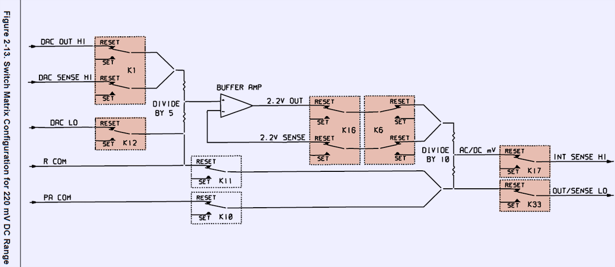
During DC operation, PA gain is -20, as determined by the 500 kΩ/25 kΩ resistor network on the HR8 assembly. Control line SW3, inverted by U8, turns on Q51. This references the +input of the precision opamp in the input stage to R COM. The DAC assembly is set to the negative 11V range and its outputs, DAC OUT HI and DAC SENSE HI, are connected to pin 2 of the resistor network on the HR8 assembly by relay K2. The sense current cancellation circuit is active during DC operation. Its output, SIG1, is connected to the resistor network feedback resistor pin 1 by relay K15A. The amplifier has a much lower bandwidth in this mode because of the much higher Miller capacitance in C57. Lower bandwidth results in lower amplifier noise.
The output signal, PA OUT HI, is routed to the High Voltage Control assembly (A14), where it goes through relay K10 and becomes PA OUT DC. PA OUT DC is routed to the Switch Matrix for connection to the OUTPUT HI binding post. The sense signal, PA SENSE DC from the Sense Current Cancellation circuit, is routed to the Switch Matrix assembly (A8) for connection to the OUT/SENSE HI or SENSE HI binding posts, thus making the binding post the sense point in internal sense and allowing for external sense through the SENSE HI binding post.
PA Operation: 220V AC Range
During AC operation, PA gain is -10 as determined by the 4.99 kΩ input resistor R17, and 49.9 kΩ feedback resistors (R11 + R12 + R13). Control line SW3 turns Q50 on, which references the +input of the precision opamp in the input stage to OS COM. The Oscillator assembly (A13) is set to the 22V range and its output OSC OUT HI is connected to the input resistor R17 by relay K10A. The PA output is connected to the feedback resistors R11-R13 by relay K12B. The PA output is attenuated by a precise 1/100 by 220V range ac attenuator. The attenuated signal is connected to OSC SENSE HI, where it is sent to the Oscillator Control assembly (A12).
The Oscillator Control assembly regulates the Oscillator Output so that an exact calibrated AC signal appears at OSC SENSE HI. Since the 220V range AC attenuator is completely characterized (as explained below), the exact desired signal appears at PA SENSE AC and hence at the appropriate sense point at the output.
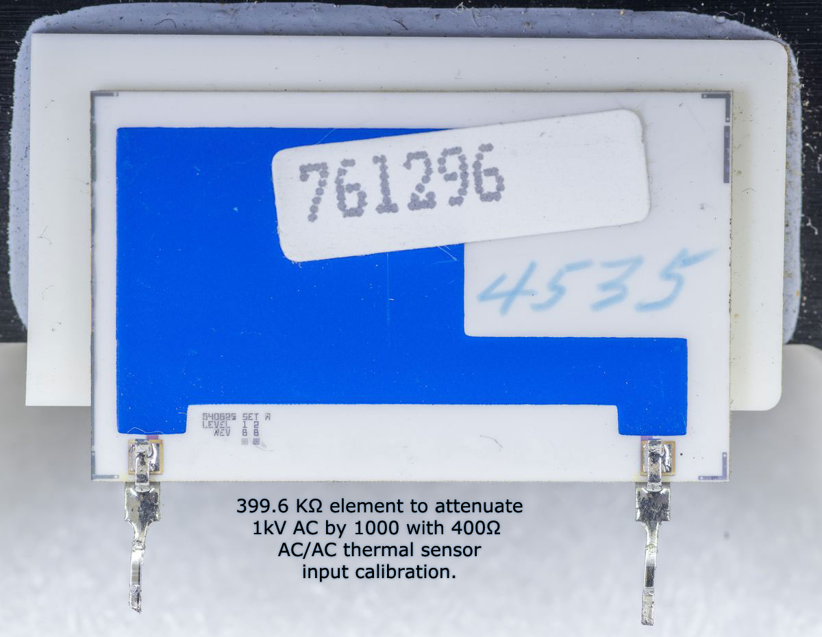
The 220V range AC attenuator circuit contains opamp U4, a 400 kΩ/4 kΩ resistor network Z1, and transistor Q54. PA SENSE AC, which is connected to PA OUT HI at the load, is connected to the 400 kΩ input resistor (pin 1) of Z1 by relay K16. The 400 kΩ/4 kΩ node (pin 3) of Z1 is connected to the inverting input of U4. During AC operation, control line C0* is inverted by U8, which turns on Q58 to connect the non-inverting input to OSC RCOM. Transistor Q54 supplies current gain for the output of U4 to drive the capacitance of the OSC SENSE HI line. This voltage is connected to the 4 kΩ feedback resistor (pin 4) of Z1. The output is connected to OSC SENSE HI by relays K10B and K11.
The DC feedback 500 kΩ/25 kΩ resistor network and the sense-current cancellation circuitry are disconnected by energizing K15. The sense signal, PA SENSE AC, and the output signal, PA OUT HI, are routed to the High Voltage Control assembly (A14), where relays K10, K13, and K3 connect them to HV SENSE and HV OUT. HV SENSE and HV OUT are connected to the binding posts by the motherboard relays in the same manner as in the 1100V high voltage mode. Refer to the High Voltage assembly theory of operation in service manual for more information.
220V DC Internal Calibration Network
The 220V DC internal calibration network determines the exact gains and offsets of the PA. This circuit uses part of the resistor network HR8 as the input attenuator, and uses opamp U9, and zener diodes VR57 and VR58. Relay K4 connects the output of this circuit to the RCL line. Zener diodes VR57 and VR58 reduce the power supplies for chopper-stabilized amplifier U9, which is used as a voltage follower.
Power supply design for A11
This section will cover design of power supply board to power up A11.
Fluke 5720A A9 Ohm Calibration board
Shield PCB for A10 Ohm main board
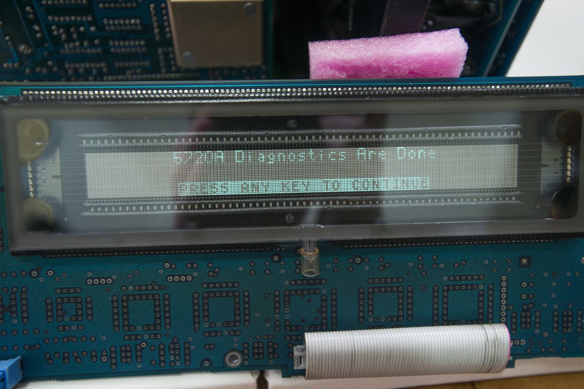
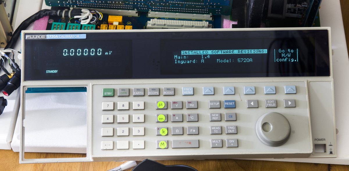
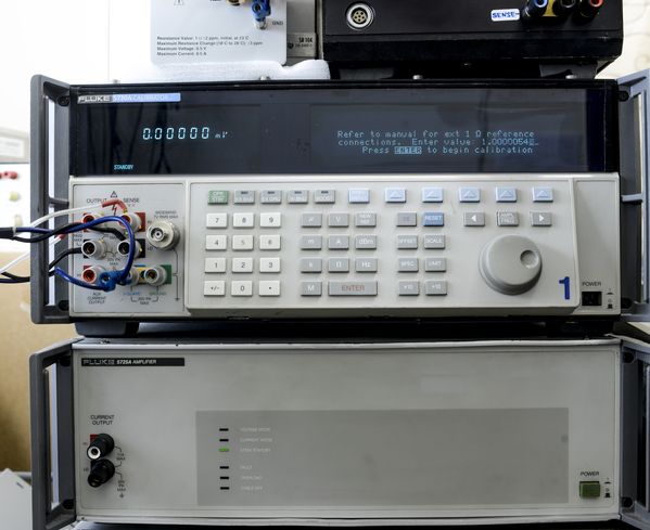
5720A Firmware testing and first power-on.
Attempt to run 5720A with old inguard firmware results in unspecified error (VFdcDac Value Out Of DAC Range, Code 4500).
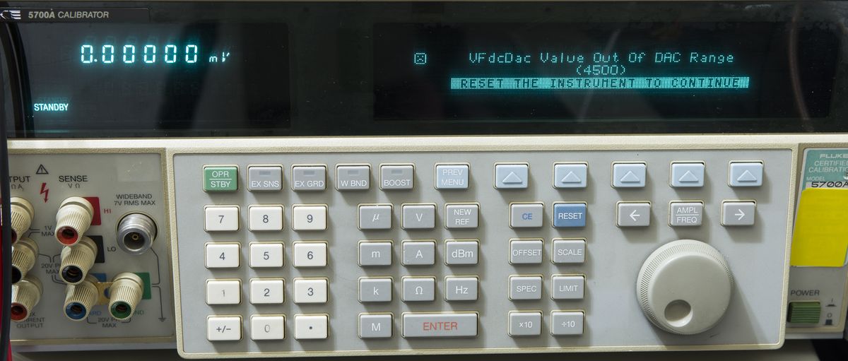
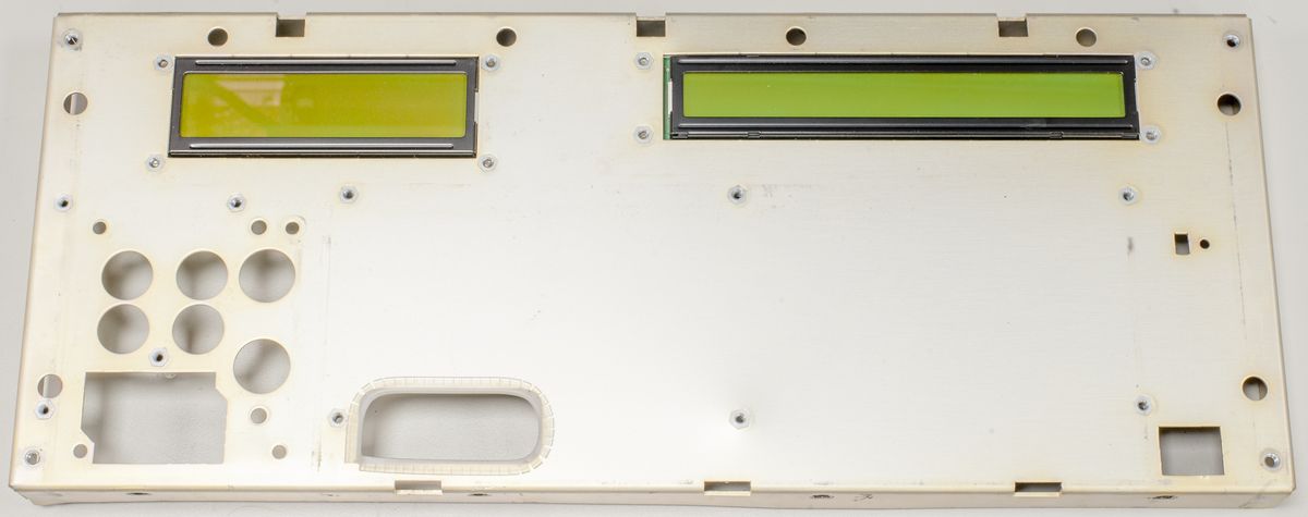
Front panel modification
Overview of A10 Ohms Main PCBA from Fluke 5700A MFC
The Ohms function for the 5700A is provided by two plug in circuit boards, the Ohms Main assembly A10 and the Ohms Cal assembly A9. I’ve bought faulty A10 board, so we can study resistor networks and overall design of this switchable resistance standard. These two assemblies function as one module in calibrator to supply fixed values of resistance, from 1Ω to 100 MΩ. Resistances are available in values of 1×10Ω (for example 1, 10, 100, 1k…100M) and 1.9×10Ω (1.9, 19, 190 and so on, up to 19M). There is also short zero reference and 2-wire 100 MΩ resistor. Also there is switching implemented to allow calibration of each resistance path to external standard.
These assemblies are also used to calibrate the 5700A Current function. The A10 PCBA contains all the resistor values except the 1Ω, 1.9Ω, and short, which are located on the A9 PCBA. It also contains the relays and their drivers to switch these values as requested under program control. The A9 PCBA contains all calibration circuits except for one op amp on the A10 PCBA. It also contains a circuit to provide accurate calibration of twowire ohmmeters. In addition, there are relays, relay drivers, and logic to interface the Ohms assemblies to the digital bus. Refer to Figure 2-30 for a simplified schematic of both the Ohms Main and Ohms Cal assemblies.
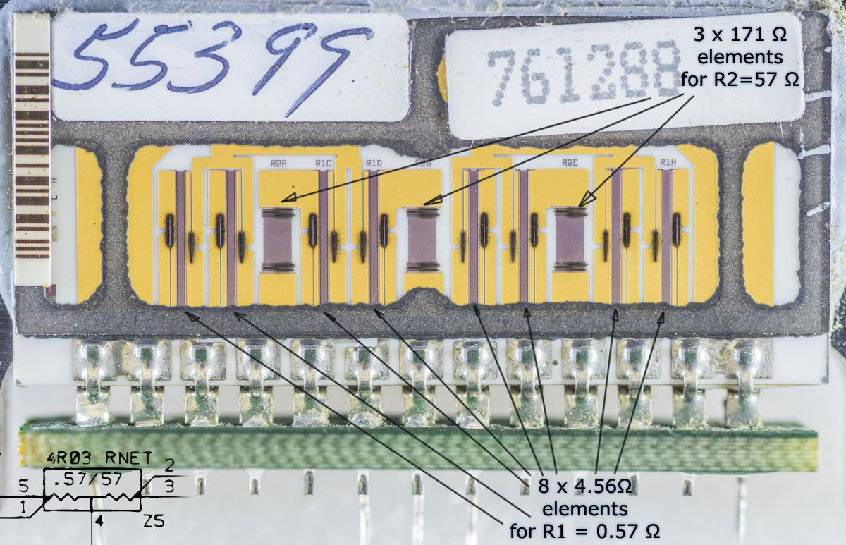
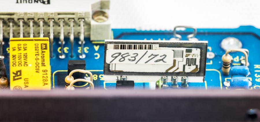
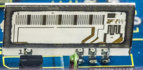
The A10 PCBA uses three Fluke hermetically-sealed thin film resistor networks Z1, Z2 and Z3 to obtain values from 10Ω to 19 MΩ. The values are arranged in two strings, one for decade values and the other for the multiples of 1.9. The 100 MΩ value is achieved by inserting a 90 MΩ film resistor (R1) in series with the decade string.
Power supply design for A10
This section will cover design of power supply board to power up A10.
Power supply design for A6
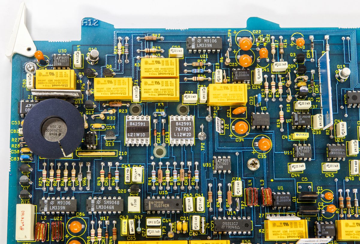
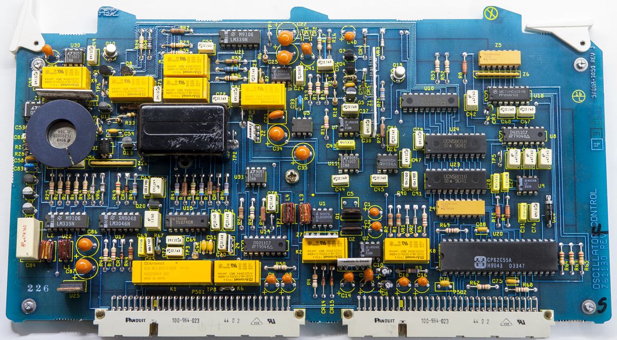
Overview of A12 Oscillator Control PCBA
The Oscillator Control assembly (A12) contains all the precision ac amplitude control circuitry except the output AGC amplifier, which is located on the Oscillator Output assembly (A13). The primary function of the Oscillator Control assembly is to monitor the output of the 5700A in the ac voltage function, and to adjust the output until the RMS voltage across the SENSE point is equal to the voltage requested by the operator. This assembly provides amplitude control for both the ac current function and the Wideband AC Module (Option -03) during low-frequency operation.
The oscillator control circuitry contains an averaging converter, an error intergrator, a three-pole filter, an ac/dc thermal transfer circuit, an ac/ac thermal transfer circuit, a 15-bit DAC, and a digital control circuit.
The Oscillator Output assembly generates an ac sine wave from 0.22V to 22V with a frequency range of 10 Hz to 1.1999 MHz. There are five frequency ranges (100 Hz, 1kHz, 10 kHz, 100 kHz and 1 MHz) and two voltage ranges (2.2V and 22V). The output signal is either routed to the OUTPUT binding posts, or it is used internally by the Power Amplifier, High Voltage, Wideband AC Module, Current, or Switch Matrix assemblies, or it is routed to an Auxiliary Amplifier for generation of voltages and/or functions outside this range. Output sensing is available for all voltage ranges above 220 mV at the SENSE binding posts.
The Oscillator Output assembly contains a fixed-amplitude quadrature RC oscillator, a 0.22-22V digital/linear gain-controlled amplifier, a fixed-amplitude variable phaseshifting network, phase-locked loop control circuitry for phase locking to an external signal or the PLOCK signal from the Current/Hi-Res assembly (A7), and digital control circuitry.
Power supply design for A12
All power supplies used by this assembly are generated by the Guard Crossing/Regulator assembly (A17) except the +5 OSC supply, which is generated by a three-terminal +5V regulator (U25) from the +15 OSC supply. The ±15 OSC supplies are buffered by L3, L4, C34 and C35 to create the ±15A supplies, and L1, L2, C86 and C87 to create the ±15B supplies. A +2.5V reference voltage is created from the +5LH supply by resistors R52 and R53. A -200 mV reference voltage is created from the -15V OSC supply by resistors R57 and R58 for use exclusively by the protection circuitry for thermal sensors U14 and U16.
A14 assembly
Second A12 board
A13 – Oscillator output board
Wideband option A5 – Output PCBA from Fluke 5700A MFC
Fluke 5700/5720A have option 03 to get Wideband output functionality. It is delivered by two additional modules, A5 and A6, working in tandem to generate precision sinewave output with frequency range 10 Hz to 30 MHz. Signal amplitude can be programmed from 300 µV to 3.5 V directly in voltage units or from -57 dBm to +24 dBm power level when referenced to 50 Ω impedance.
| WBV Range | Resolution | Absolute Uncertainty, 1 year (24 hour), 30 Hz – 500 kHz |
|---|---|---|
| 1.1 mV | 10 nV | ±0.8% + 2 µV (±0.4% + 0.4 µV) |
| 3 mV | 10 nV | ±0.7% + 3 µV (±0.4% + 1 µV) |
| 11 mV | 100 nV | ±0.7% + 8 µV (±0.2% + 4 µV) |
| 33 mV | 100 nV | ±0.6% + 16 µV (±0.2% + 10 µV) |
| 110 mV | 1 µV | ±0.6% + 40 µV (±0.2% + 40 µV) |
| 330 mV | 1 µV | ±0.5% + 100 µV (±0.2% + 100 µV) |
| 1.1 V | 10 µV | ±0.5% + 400 µV (±0.2% + 400 µV) |
| 3.5 V | 10 µV | ±0.4% + 500 µV (±0.15% + 500 µV) |
The Wideband Output A5 PCBA takes the sine wave signal from either the WBV A6 PCBA or the main A12+A13 PCBA, and amplifies it to a power level that drives 3.5 V into a 50 Ω load at the output. The A13 generates the sine wave signal from 10 Hz to 1.1999 MHz, and the WBV A6 generates the sine wave signal from 1.2 MHz up to 30 MHz. A6 have fast power amplifier circuit that increases the gain and power level of the input signal to drive load.
Unlike normal AC Voltage function operation wideband output cannot be phase-locked to external reference frequency, so frequency uncertainty specified as 0.01%. Accuracy of the wideband output is maintained by separate calibration constants, and calibrator have special calibration procedures for both gain and flatness correction factors. Gain can be self-calibrated using Type N 50Ω feedthru terminator, short Type-N cable and Type N female to dual banana post adapter. Wideband Flatness calibration require external reference, such as Fluke 5790A or thermal converter setup.
| WBV Frequency ranges | Frequency resolution | Amplitude flatness vs 1 kHz reference, >3 mV | TC | Harmonic Distortion |
|---|---|---|---|---|
| 10 – 30 Hz, bypassed from ACV | 0.01 Hz | ± 0.3% | ± 100 ppm/K | -40 dB |
| 30 – 120 Hz, bypassed from ACV | 0.01 Hz | ± 0.1% | ± 100 ppm/K | -40 dB |
| 120 – 1200 Hz, bypassed ACV | 0.1 Hz | ± 0.1% | ± 100 ppm/K | -40 dB |
| 1.2 – 11.999 kHz, bypassed ACV | 1 Hz | ± 0.1% | ± 100 ppm/K | -40 dB |
| 12 – 120 kHz, amplified ACV | 10 Hz | ± 0.1% | ± 100 ppm/K | -40 dB |
| 120 – 1199.9 kHz, amplified ACV | 100 Hz | ± 0.1% + 3 µV | ± 100 ppm/K | -40 dB |
| 1.2 – 2 MHz, WBV generated | 100 kHz | ± 0.1% + 3 µV | ± 100 ppm/K | -40 dB |
| 2 – 10 MHz, WBV generated | 100 kHz | ± 0.2% + 3 µV | ± 100 ppm/K | -40 dB |
| 10 – 20 MHz, WBV generated | 1 MHz | ± 0.4% + 3 µV | ± 150 ppm/K | -34 dB |
| 20 – 30 MHz, WBV generated | 1 MHz | ± 1% + 3 µV | ± 300 ppm/K | -34 dB |
A5 assembly handle function switching, frequency ranges and perform AC to AC conversion for precise amplitude control using custom Fluke Thermal Sensor ASIC, similar to how ACV A12 assembly does for normal frequency outputs. Wideband output attenuator and gain correction circuitry also located on this board. This board works together with wideband filter A6 PCBA.
Modern Fluke 5730A have combined A5 and A6 into single upgraded wideband assembly, which also extend frequency range to 50 MHz. This frequency often used as reference point for power sensor calibration.
Wideband option A6 – AC Oscillator PCBA from Fluke 5700A MFC
This PCBA have oscillator and discrete filter circuits for each of the wideband frequency ranges. In wideband range operation A5 provide square wave signal with correct amplitude and frequency which is converted to sine wave by one of the five-pole filters on A6.
This variable frequency and amplitude sine wave is routed to the Wideband Output assembly via SMA connector J1 and a 75 Ω coaxial cable between the boards.
Extenders for repairs and troubleshooting
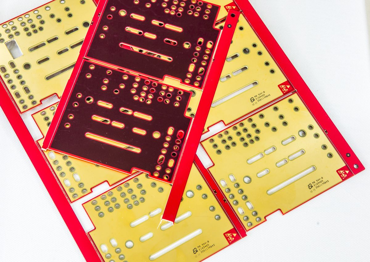
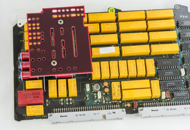
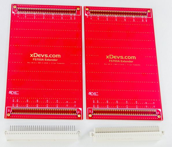
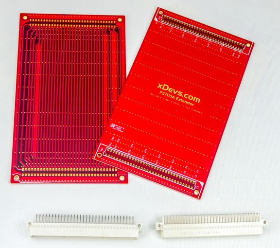
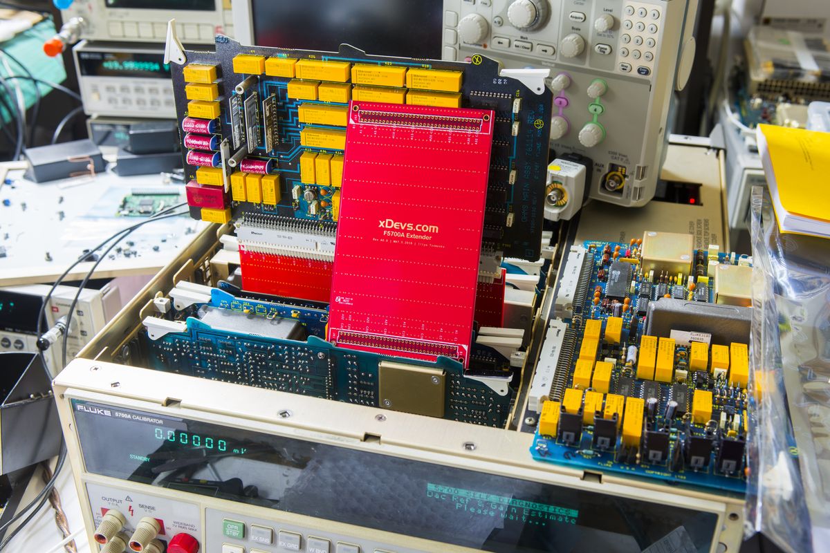
To help with probing boards in calibrator during repairs we designed inhouse extender adapters PCBs. These are built to lift the card outside of the mainframe enclosure while still providing electrical connections and operation of the calibrator. Such extension board allow to measure various test points on the circuit board under different modes and functions of the calibrator.
These extenders used 4-layer TG150 1.6mm PCB and were very helpful with troubleshooting and repairs.
Fluke 5725A ‘Booster’ amplifier for voltage/current ranges extension
To complete the project, xDevs.com also acquired range extender amplifier, in parts/unknown condition state. This section of the article address design, troubleshooting and testing of the 5725A together with our 5720A unit.
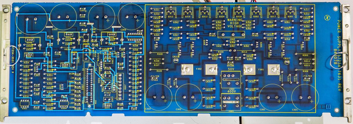
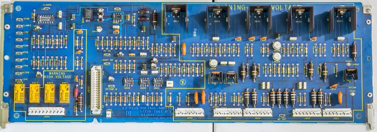
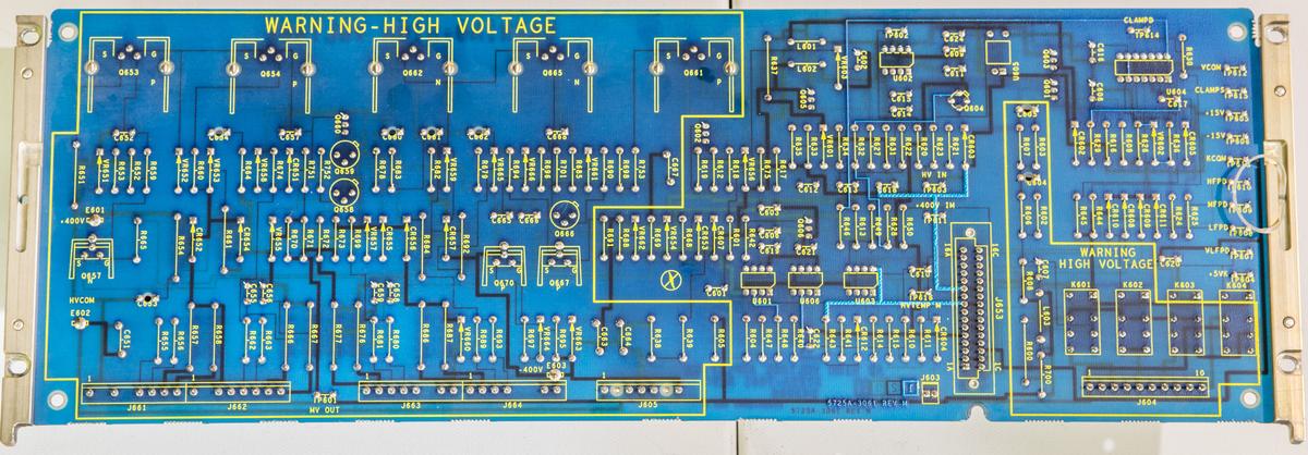
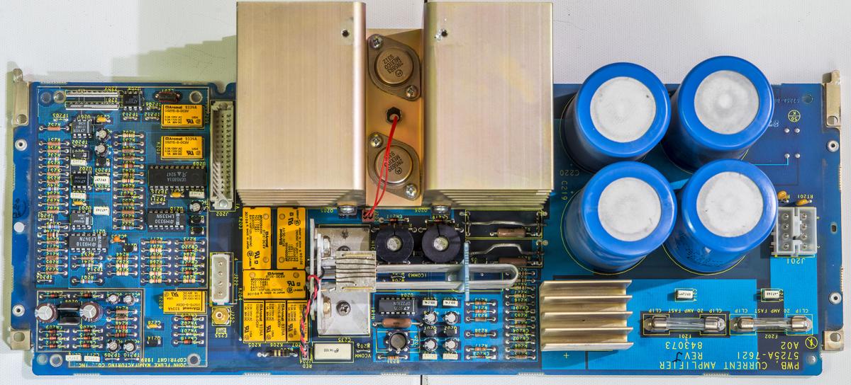
The Fluke 5725A Amplifier enhances performance and ranges of the 57xx series MFC with AC Voltage, AC Current, and DC current functions. Amplifier (also often referred as Booster) compatible only with Fluke 5500A, 5700A, 5700A/EP, 5720A and 5730A series calibrators. Model 5520A/5522A calibrators cannot work with 5725A amplifier.
The 5725A operates under complete control of the 5700/5720/5730A through an special interface cable. A diagram in the Fluke 57xx specifications tables illustrate the extended AC volt-hertz product achieved by using a 57xxA with 5725A. Increased AC voltage load limits also allow using the calibrator in systems with long cables.
Voltage output from the 5725A is available at the 5700A Calibrator front or rear binding posts. This eliminates the need to move cables during a procedure that requires amplified as well as standard calibrator outputs.
The 5725A front or rear panel OUTPUT binding posts are only for current output. Extended-range AC and DC current is supplied through them. Since most meters with a high current range use a separate high current input terminal, this configuration normally eliminates the need to move cables during a procedure. If a single-point current output is needed, the calibrator can be configured to source all current outputs through the 5725A binding posts.
Enhancements to 5700A ACV output capability provided by the 5725A are as follows:
- Frequency limits at higher voltage increase to 100 kHz at 750 VAC or 30 kHz at 1100VAC.
- Load limits are to 70 mA for frequencies above 5 kHz, and to 50 mA for frequencies less than 5 kHz.
- Capacitive load limits are increased to 1000 pF.
Model 5725A amplifier is only used operating these functions and ranges:
- AC voltage: 220 to 1100V RMS up to 70 mA (50 mA < 5 kHz), 40 Hz to 30 kHz; 220 to 750V RMS up to 70 mA, 30 kHz to 100 kHz
- DC current: 0 to ± 11A
- AC current: 1 to 11A RMS, 40 Hz to 10 kHz

Image : Complete set, Fluke 5700A multi-function calibrator with Fluke 5725A voltage/current amplifier
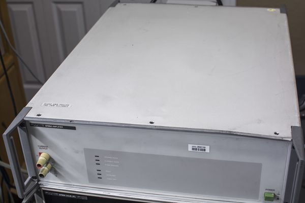
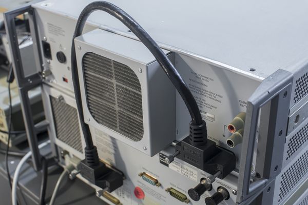
Image : Top and rear sides of the Fluke 5725A with 5700A.

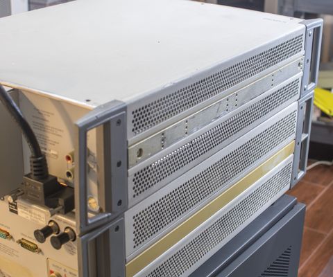
Image : 5725A have vents for coolant airflow from both sides. Keep that in mind for lab orientation.

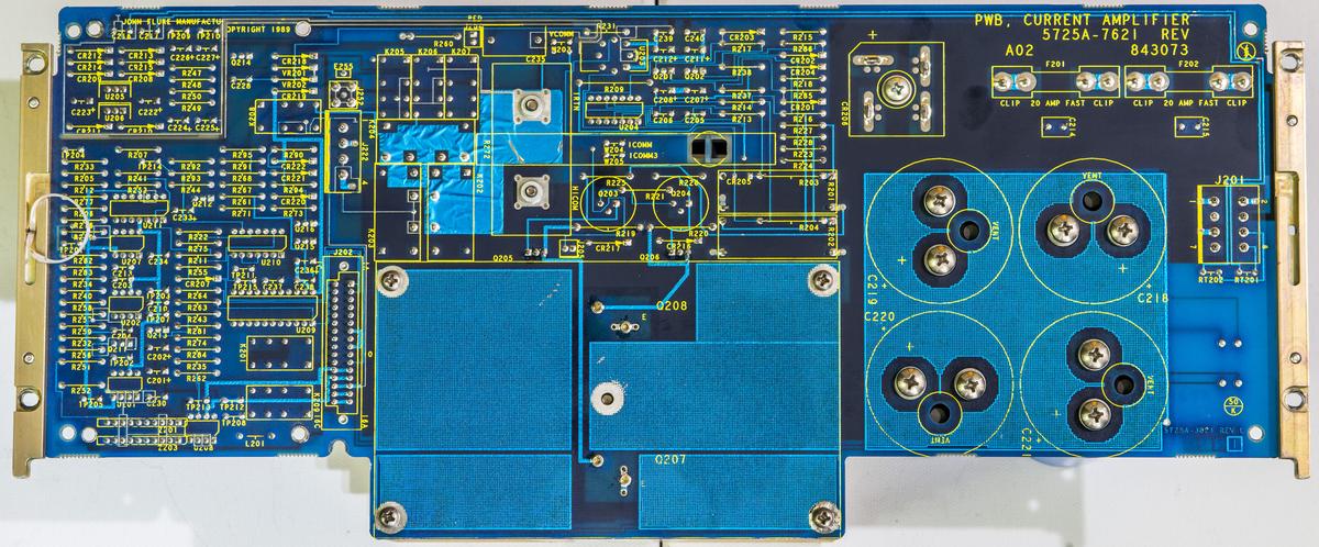
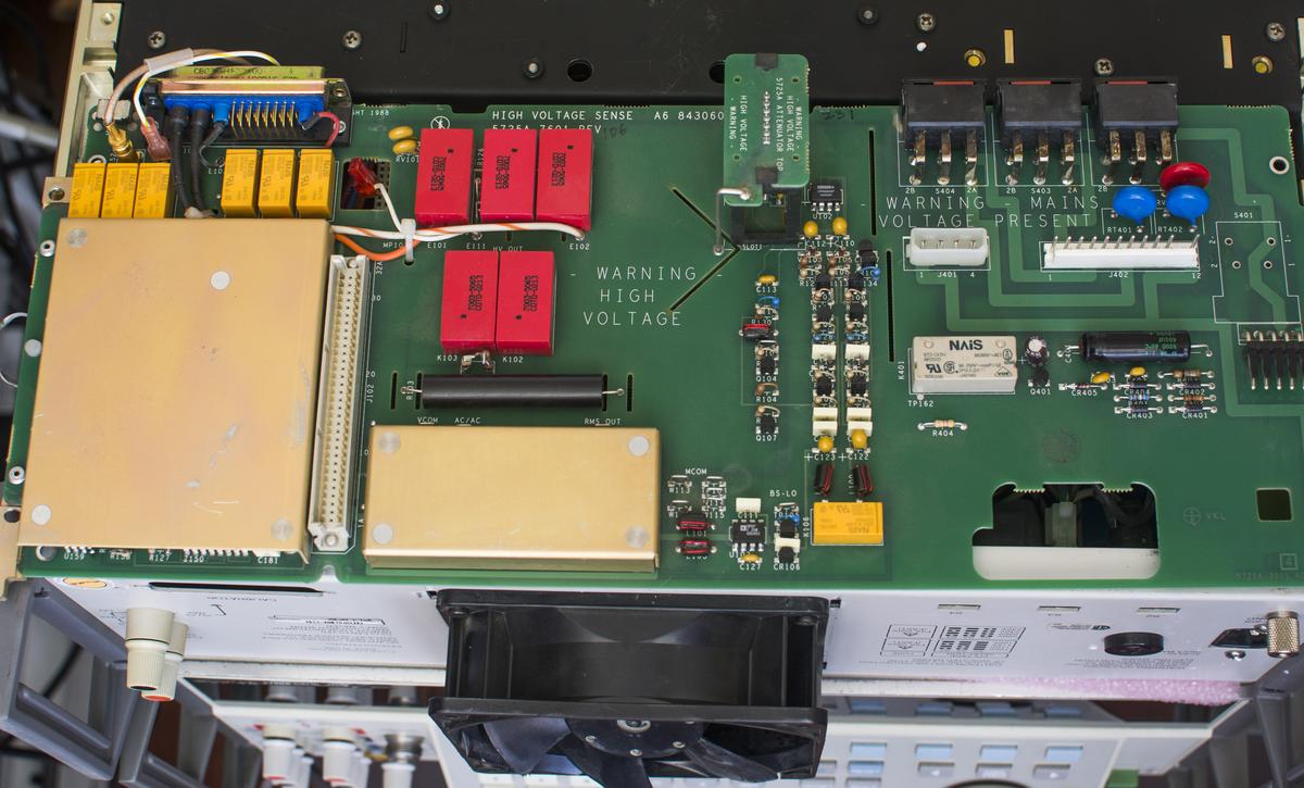
High-voltage/high-current energized circuits present inside amplifier when powered on, even when standby! Service can be dangerous and even lethal. Pay attention of what you are doing, and keep all connections stable and robust, not using hand probing unless absolutely required and safe. Use tools rated for CAT III operation while servicing high-power circuits in this instrument. Do not service alone.
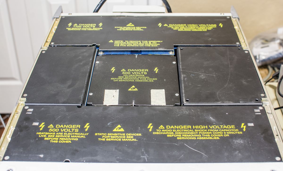
Image : Top metal cover removed, revealing lethal compartments and modules
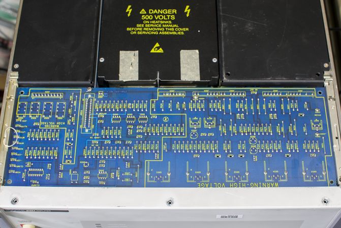
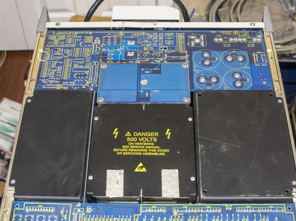
Image : PCBA covers removed, showing thru-hole assembly design
All boards were visually verified for any physical damages, like leaky capacitors, damaged traces or burnt components. Fuses were tested and confirmed good. High-voltage amplifier MOSFETs on heatsinks were probed and confirmed good. Interconnect cables visually had no issues as well.
After such checks first booster power on test it was commited, and all internal voltage rails like -400, +400, midstage filter supply, ±20V, ±15V and 5V relay power were verified in spec. This ruled out obvious power supply problems.
Carbon composite resistors on PA and power supply board were replaced with brand new metal film and non-inductive wirewound resistors, as preventive maintenance. All large electrolytic capacitors, except 50000 µF 20V on current amplifier board were replaced with brand new modern +105 °C capacitors. We follow usual rule to replace all electrolytic caps after 10 years. This particular 5725 was build in 1992, so caps are long overdue. Remember, 5725A is high-power device with planned long peroids of unattended runtime. It is wise to reduce risk of electrical failures and fire hazards by investing a little into good capacitors and parts.
Initial diagnostics revealed major problems with amplifier operation in voltage operate mode. Unit was not able to source any AC voltage and was tripping 5720A to standby after few seconds on low frequency (40Hz-1kHz) or even faster on higher frequencies. 5720A also giving random 5725A diagnostics errors when 5725A goes into fault mode, sometimes reporting Fan not working, sometimes HVCLAMP activated, or just going to “Output tripped to standby” errors.
Measurements of HV IN signal on A3 PA board or at input connector on HV sense A6 board give out first suspect – the interconnect cable. From theory of operation one can learn that 5725A in voltage mode provide fixed gain x100 for the input voltage signal from calibrator’s A12 oscillator board. 5725A generate high-voltage output, precisely attenuate it 100 times and provide feedback signal back to calibrator thru the interconnect cable. Calibrator then uses it’s AC/DC thermal convertor on A12 oscillator to fine-tune output into 5725A to provide precise HV output. So it is crucial for interconnect cable to provide good connections and signal integrity for whole setup to operate correctly.
In simple example, to achieve precise 250 VAC, 1kHz signal calibrator will source 2.5 VAC 1 kHz into 5725A, and get 2.5 VAC 1kHz feedback output, that is divided output of the expected 250 VAC. If the feedback signal or input from calibrator have leakage or bad connection, feedback loop will be open and none of this would work. Random errors from calibrator when 5725A trips to failure mode also suggest bad ground/return path or coupling issues that may be result of open connection or cold joint in cable harness.
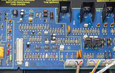
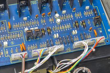
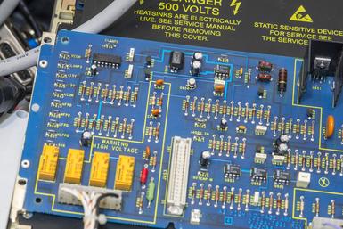
Image : PCBA covers removed, showing thru-hole assembly design
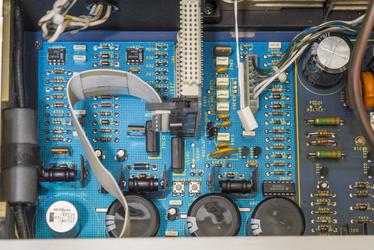

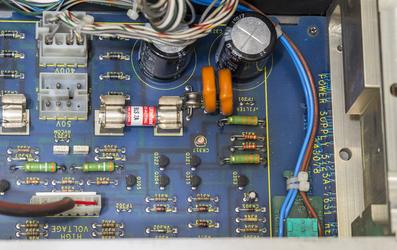
Image : PCBA covers removed, showing thru-hole assembly design
Interesting enough, 5725A operated correctly and pass self-test diagnostics for AC/DC amplifiet current outputs just fine. Most of the voltage analog signal lines are not used when used in current boost mode, so that would suggest at least partically functional cable. It also gives better confidence that digital section and interfacing in our 5725A is working fine.
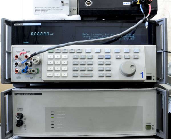
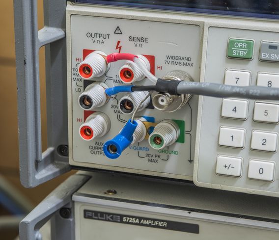
Making DIY test interconnect cable between Fluke 5720A and booster
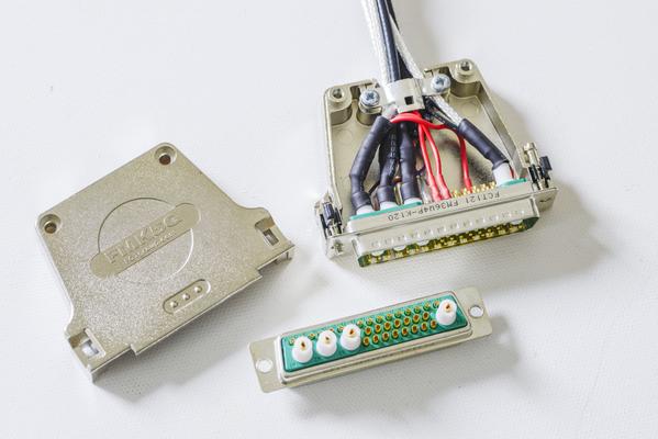
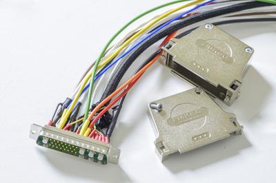
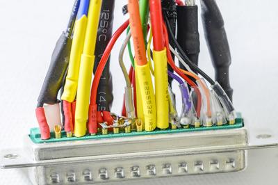
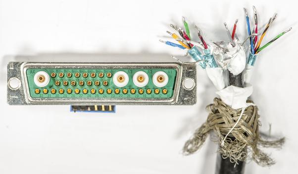
To rule out bad cable, we decided to build DIY alternative to with all expected connections between 5725A and 5720A. Specialized DB-type connector with high-voltage PTFE inserts was purchased from Digikey for this experiment. Choice of wires was also tricky, due to high-voltage AC signals travelling between the units, so we ended up as next harness concept:
- Digital connection used shielded multi-wire cable, with shield connected to V-GRD
- Boost-in, boost-sense hi signals are wired by Keithley low-noise coax, with shield connected to V-GRD
- Boost-out also wired by same Keithley low-noise coax, with own V-GRD on shield
- Current input signal wired by PTFE twinax cable, shield connected to I-GRD
- B-RCL line which carry precision feedback back into 5720A wired using Gore low triboelectric noise coax. Shield connected to V-GRD
- Boost sense lo and PA-COM connected between units with AWG22 600V PVC wires.
It took quite a while for me to determine where guards should go and what signals to shield. Because calibrator can provide all current ranges at the 5725A booster current output terminals, it is important to provide current guarding to avoid low currents leakage and errors on most sensitive 220 µA range.
Connectors used in this DIY cable, from Digikey retail store:
| Qty | Digikey P/N | Manufacturer P/N | Description | Price, 1 pcs | Subtotal |
|---|---|---|---|---|---|
| 8 pcs | WM12525-ND | Molex LLC FMV001P-K 1727040134 | FCT TERM HVOLT STR PC PLG | 6.43 | $51.44 |
| 2 pcs | WM12511-ND | Molex LLC FMK 1727040104 | FCT HOOD S5 0 DEG MTL W/SCRWLCK | 15.27 | $30.54 |
| 2 pcs | WM12558-ND | Molex FCT 1731070071 | CONN D-SUB PLUG 36POS PNL MNT | 15.29 | $30.58 |
Total cost for DIY cable, not including the wires and hours of work to assemble it – $113 USD.
Fluke’s instruction manual and service manual for 5700/5720A do not clearly show harness diagram or type of wire used for this interconnect cable, so hopefully this DIY build can be good enough for initial testing of our “bad cable theory”.
After power on, 5725A was detected by 5720A correctly, and first check of current function operation confirmed good output with both 11 ADC and 11 AAC 40Hz…10kHz outputs. First test with voltage operation and 220V 1kHz from 5725A revealed that function now works! Further checks with Fluke 87V as DUT AC meter at the 5720A output terminals revealed correct output including 1000V 40Hz and 1kHz signals.
750VAC 100kHz without DUT connected also did not cause any faults or errors. Winner winner, chicken dinner! Rare case when repair of the unit revealed that…no repair was necessary, only interconnect cable replacement.
It may not look as much, and all the random wires were too large to fit into Molex housing nicely, but it does indeed function correctly for time being, before correct harness is build/sourced.
Design of original Fluke interconnect cable
Original Fluke interconnect cable had few revisions. Bad cable that we have here for teardown and repair attempt is Fluke P/N xxxxxx, with right-angled cable dressing and overmolded rubber housing. Hopefully we will be able to remove D-SUB plugs without cutting too much of precious custom Fluke cable, so it can be checked and reused with new D-SUB connectors to make good DIY cable for further use.
Cable itself is fully shielded and all interconnect at the connector side is completely filled with semi-transparent epoxy. It makes simple repair impossible, but reasons to do such rugged design are clear as well. 57xx series calibrators and amplifier may be used in harsh field environments with high ambient temperature and humidity conditions, so transferring outputs at 1100VAC 30kHz need extra care to be safe and reliable.
Outer epoxy surface is completely covered with copper adhesive tape.
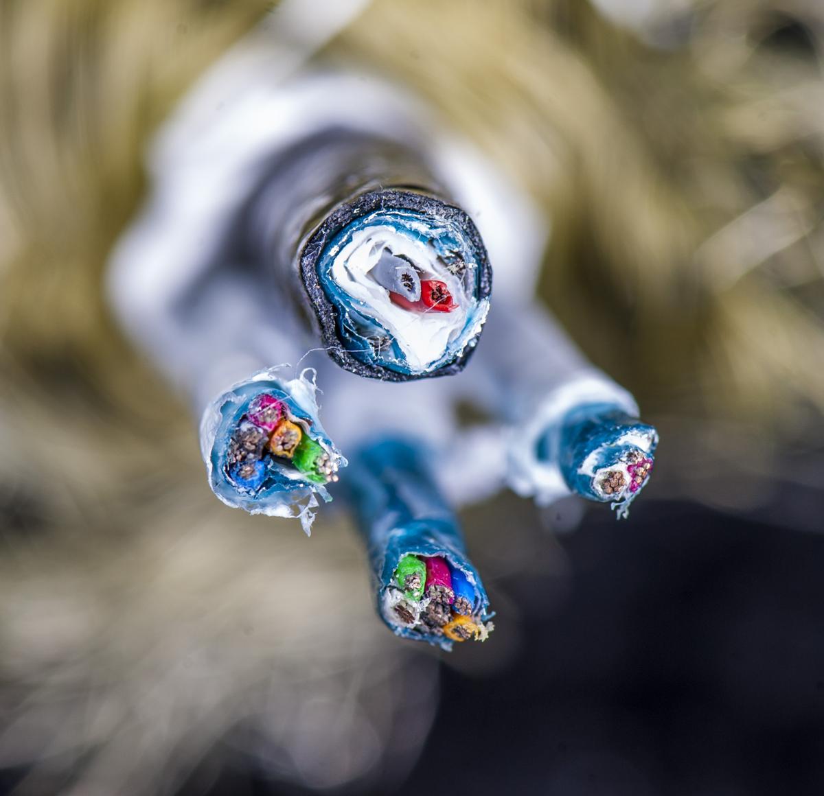
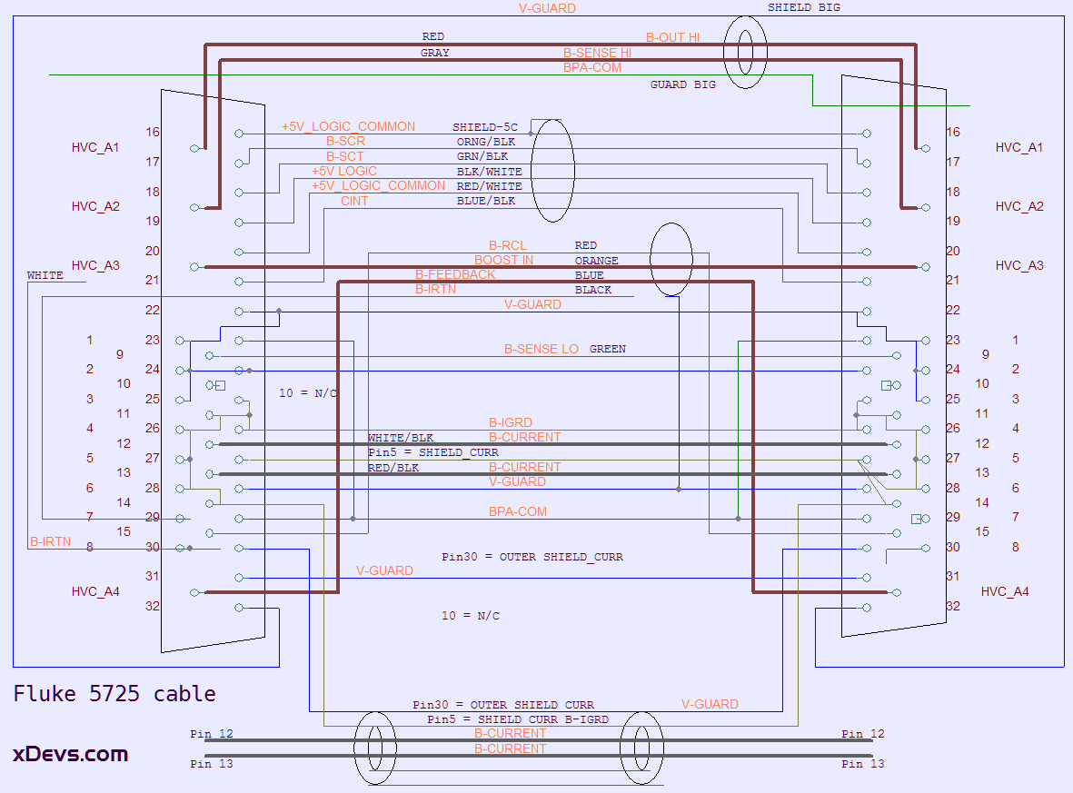
Here is reverse-engineered wiring harness diagram of original Fluke 5725 interconnect cable. Not all pins are connected, for example I-GRD connects only by pin 5.
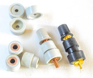
Whitening 5-way binding posts, cure old yellow aging
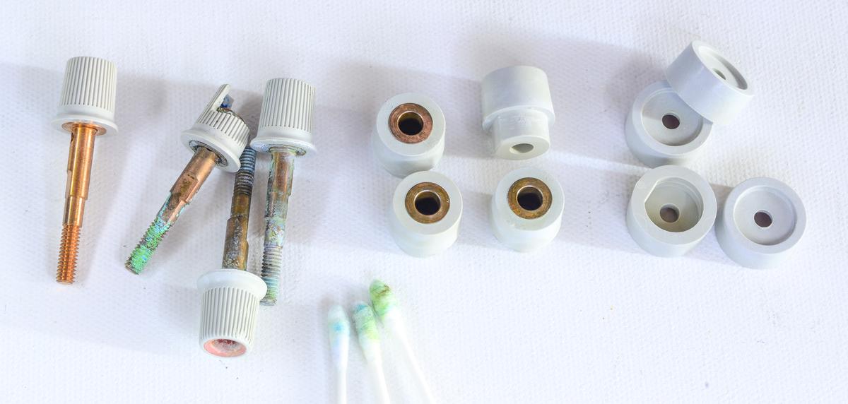
Don’t know why, but old aged plastics with prominent yellow tint bother me a bit. So I’ve tried usual treatment with peroxide bleach, and put old Fluke posts from 5725A amplifier out to the UV rays from sun.
That did remove yellow tint from plastic. In the process of doing so copper got unhappy and oxidized into pretty green crystals, following expectations.
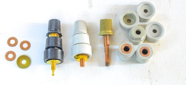
Not to worry, actual top post I already had a donor spare, with nice shiny metal surface. So only had to restore clean copper shine on the “base” part of the post, which actually only provides support for moving post and not the main electrical carrier.
Black Model 2758 Low Thermal EMF Binding Posts is shown for comparison. As you can see, it is nearly identical configuration to one used by Fluke, other than black plastic color and gold plating on top of copper.
Calibration tests
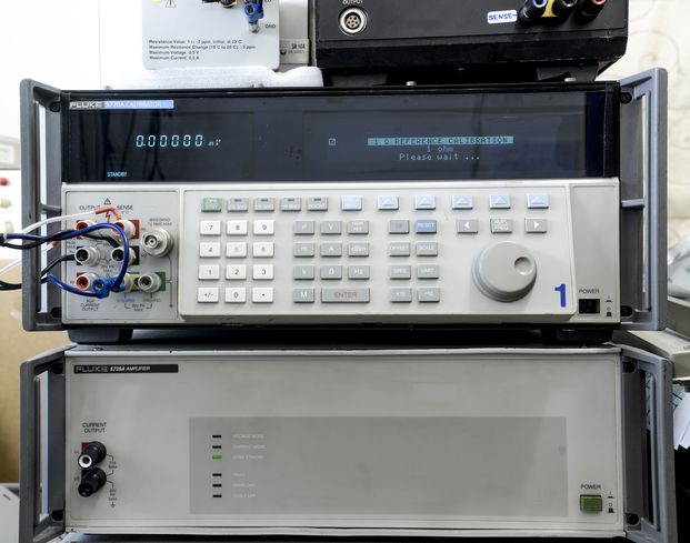
Resistance output calibration 8/15/18, versus Fluke SL935 1 and 10000 Ω
| Calibrator output | Deviation to 8/01/18 Cal | in ppm | 5720% 24hour spec, % change |
|---|---|---|---|
| 0.9998039 Ω | 0.0000428 Ω | 42.80 ppm | 85.00 ppm, (50.36) |
| 1.8998703 Ω | 0.0001237 Ω | 65.12 ppm | 85.00 ppm, (76.61) |
| 10.000290 Ω | 0.000037 Ω | 3.73 ppm | 23.00 ppm, (16.24) |
| 18.999925 Ω | 0.000051 Ω | 2.71 ppm | 23.00 ppm, (11.77) |
| 100.00301 Ω | 0.00016 Ω | 1.62 ppm | 10.00 ppm, (16.18) |
| 189.99756 Ω | 0.00049 Ω | 2.59 ppm | 10.00 ppm, (25.91) |
| 1.0000085 kΩ | 0.0000019 kΩ | 1.86 ppm | 8.00 ppm, (23.19) |
| 1.9000219 kΩ | 0.0000035 kΩ | 1.82 ppm | 8.00 ppm, (22.70) |
| 9.999776 kΩ | 0.000015 kΩ | 1.54 ppm | 8.00 ppm, (19.31) |
| 18.999374 kΩ | 0.000030 kΩ | 1.58 ppm | 9.00 ppm, (17.57) |
| 99.99470 kΩ | 0.00012 kΩ | 1.16 ppm | 9.00 ppm, (12.92) |
| 189.98859 kΩ | 0.00068 kΩ | 3.59 ppm | 9.00 ppm, (39.93) |
| 0.9999808 MΩ | 0.0000017 MΩ | 1.73 ppm | 16.00 ppm, (10.84) |
| 1.8999653 MΩ | 0.0000062 MΩ | 3.28 ppm | 17.00 ppm, (19.31) |
| 9.998990 MΩ | 0.000051 MΩ | 5.08 ppm | 33.00 ppm, (15.39) |
| 18.998386 MΩ | 0.000109 MΩ | 5.76 ppm | 43.00 ppm, (13.38) |
| 100.00693 MΩ | 0.00184 MΩ | 18.41 ppm | 100.00 ppm, (18.41) |
Booster initial calibration test results
Before adjusting 5725A we captured calcheck result using <90 days calibrated Fluke 5720A “Hulk” unit as master calibrator. Output printout results:
5725:       (Most recent)   5/03/16,  23.0 Degrees C
               (Previous)   4/28/16,  23.0 Degrees C
     (Days since last cal)  946
Booster was calibrated and adjusted not too long time ago, only 946 days, May 2016.
Current calcheck data:
| 5725 AC VOLTAGE OUTPUT SHIFTS | ||||
|---|---|---|---|---|
| RANGE Point | Full Scale Shift | Deviation | 24 hour spec, 95% | % Shift from spec |
| 5725 FS | 0.002 V | 2.00 ppm | 78.64 ppm | 2.54 |
| 1100V 1.0000 kHz | -0.001 V | -1.13 ppm | 78.64 ppm | -1.43 |
| 1100V 5.000 kHz | 0.008 V | 6.89 ppm | 110.45 ppm | 6.24 |
| 1100V 10.000 kHz | 0.008 V | 7.27 ppm | 110.45 ppm | 6.58 |
| 1100V 12.00 kHz | 0.009 V | 8.10 ppm | 110.45 ppm | 7.33 |
| 1100V 15.00 kHz | 0.009 V | 8.16 ppm | 110.45 ppm | 7.38 |
| 1100V 17.00 kHz | -0.002 V | -1.59 ppm | 110.45 ppm | -1.44 |
| 1100V 20.00 kHz | 0.016 V | 14.75 ppm | 110.45 ppm | 13.35 |
| 1100V 30.00 kHz | 0.031 V | 27.90 ppm | 240.00 ppm | 11.62 |
| 750V 30.01 kHz | 0.005 V | 6.04 ppm | 244.67 ppm | 2.47 |
| 750V 40.00 kHz | 0.032 V | 42.60 ppm | 244.67 ppm | 17.41 |
| 750V 50.00 kHz | 0.020 V | 26.99 ppm | 244.67 ppm | 11.03 |
| 750V 60.00 kHz | 0.025 V | 33.79 ppm | 660.00 ppm | 5.12 |
| 750V 70.00 kHz | 0.043 V | 57.91 ppm | 660.00 ppm | 8.77 |
| 750V 80.00 kHz | 0.059 V | 79.16 ppm | 660.00 ppm | 11.99 |
| 750V 90.00 kHz | 0.097 V | 128.98 ppm | 660.00 ppm | 19.54 |
| 750V 100.00 kHz | 0.121 V | 160.90 ppm | 660.00 ppm | 24.38 |
Even without current artifact calibration 5725A output shows impressive result, with worst accuracy error 160.9 ppm (24% of it’s 24 hour specification, 946 days since CAL) at 750VAC 100kHz test point. Of course this is relative calibration, so to get absolute calibration one must perform traceable external calibration using setup with characterized Fluke 5790A or Fluke 792A AC/DC transfer unit. Later on we will be testing output of the booster with Wavetek 4920M.
| 5725 DC CURRENT OUTPUT SHIFTS | |||||
|---|---|---|---|---|---|
| RANGE Point | Zero Shift | Full Scale Shift | Deviation | 24 hour spec, 95% | % Shift from spec |
| 5725 +FS 11A | -0.00002 A | -0.00054 A | -49.12 ppm | 372.73 ppm | -13.18 |
| -FS 11A | -0.00002 A | 0.00050 A | 45.31 ppm | 372.73 ppm | 12.16 |
DC current is also within spec with very good margin, delivering relative error of -49 and +45ppm for both polarity 11ADC current level.
| 5725 AC CURRENT OUTPUT SHIFTS | ||||
|---|---|---|---|---|
| RANGE Point | Full Scale Shift | Deviation | 24 hour spec, 95% | % Shift from spec |
| 5725 1.0000 kHz | -0.0004 A | -40.56 ppm | 385.45 ppm | -10.52 |
AC current have single point at 1kHz, but booster actually able to drive up to 10kHz on 11A AC range. Relative error is even less, -40.6 ppm.
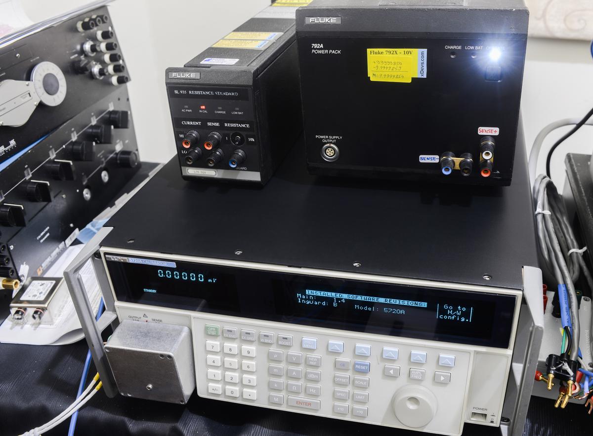
Now artifact calibration and adjustment was performed for 5720A and 5725A, using Fluke SL935 1 Ω-10 kΩ and xDevs/Fluke 792× 10VDC standards and discipline Keysight 3458A. Recorded calibration adjustment results:
| 5725 AC VOLTAGE ARTIFACT CALIBRATION OUTPUT SHIFTS | ||||
|---|---|---|---|---|
| RANGE Point | Full Scale Shift | Deviation | 24 hour spec, 95% | % Shift from spec |
| 5725 FS | 0.005 V | 4.19 ppm | 78.64 ppm | 5.33 |
| 1100V 1.0000 kHz | -0.001 V | -0.54 ppm | 78.64 ppm | -0.69 |
| 1100V 5.000 kHz | 0.008 V | 7.71 ppm | 110.45 ppm | 6.98 |
| 1100V 10.000 kHz | 0.005 V | 4.85 ppm | 110.45 ppm | 4.39 |
| 1100V 12.00 kHz | 0.002 V | 2.12 ppm | 110.45 ppm | 1.92 |
| 1100V 15.00 kHz | 0.005 V | 4.47 ppm | 110.45 ppm | 4.05 |
| 1100V 17.00 kHz | 0.004 V | 3.37 ppm | 110.45 ppm | 3.05 |
| 1100V 20.00 kHz | 0.018 V | 16.14 ppm | 110.45 ppm | 14.61 |
| 1100V 30.00 kHz | 0.036 V | 32.28 ppm | 240.00 ppm | 13.45 |
| 750V 30.01 kHz | 0.006 V | 8.44 ppm | 244.67 ppm | 3.45 |
| 750V 40.00 kHz | 0.032 V | 43.04 ppm | 244.67 ppm | 17.59 |
| 750V 50.00 kHz | 0.020 V | 26.85 ppm | 244.67 ppm | 10.97 |
| 750V 60.00 kHz | 0.021 V | 28.58 ppm | 660.00 ppm | 4.33 |
| 750V 70.00 kHz | 0.037 V | 49.36 ppm | 660.00 ppm | 7.48 |
| 750V 80.00 kHz | 0.048 V | 64.50 ppm | 660.00 ppm | 9.77 |
| 750V 90.00 kHz | 0.082 V | 108.80 ppm | 660.00 ppm | 16.49 |
| 750V 100.00 kHz | 0.110 V | 147.28 ppm | 660.00 ppm | 22.31 |
| 5725 DC CURRENT ARTIFACT CALIBRATION OUTPUT SHIFTS | |||||
|---|---|---|---|---|---|
| RANGE Point | Zero Shift | Full Scale Shift | Deviation | 24 hour spec, 95% | % Shift from spec |
| 5725 +FS | 0.00002 A | -0.00057 A | -51.80 ppm | 372.73 ppm | -13.90 |
| -FS | 0.00001 A | 0.00060 A | 54.54 ppm | 372.73 ppm | 14.63 |
| 5725 AC CURRENT ARTIFACT CALIBRATION OUTPUT SHIFTS | ||||
|---|---|---|---|---|
| RANGE Point | Full Scale Shift | Deviation | 24 hour spec, 95% | % Shift from spec |
| 5725 1.0000 kHz | -0.0005 A | -44.82 ppm | 385.45 ppm | -11.63 |
Deviations are well in line and agree well to the Calcheck data prior to artifact calibration, as they as should for properly working calibrator and transfer procedures.
Calibration Check procedure was executed shortly after the ACAL to confirm correct internal values transfer as well. Relative shifts for 1 hour presented in tables below.
| 5725 AC VOLTAGE CAL CHECK OUTPUT SHIFTS | ||||
|---|---|---|---|---|
| RANGE Point | Full Scale Shift | Deviation | 24 hour spec, 95% | % Shift from spec |
| 5725 FS | -0.002 V | -1.62 ppm | 78.64 ppm | -2.07 |
| 1100V 1.0000 kHz | 0.006 V | 5.17 ppm | 78.64 ppm | 6.58 |
| 1100V 5.000 kHz | -0.006 V | -5.20 ppm | 110.45 ppm | -4.70 |
| 1100V 10.000 kHz | 0.001 V | 1.26 ppm | 110.45 ppm | 1.14 |
| 1100V 12.00 kHz | 0.002 V | 1.60 ppm | 110.45 ppm | 1.45 |
| 1100V 15.00 kHz | -0.004 V | -3.70 ppm | 110.45 ppm | -3.35 |
| 1100V 17.00 kHz | 0.001 V | 0.91 ppm | 110.45 ppm | 0.82 |
| 1100V 20.00 kHz | 0.002 V | 1.37 ppm | 110.45 ppm | 1.24 |
| 1100V 30.00 kHz | -0.001 V | -0.93 ppm | 240.00 ppm | -0.39 |
| 750V 30.01 kHz | -0.001 V | -1.36 ppm | 244.67 ppm | -0.56 |
| 750V 40.00 kHz | -0.001 V | -1.71 ppm | 244.67 ppm | -0.70 |
| 750V 50.00 kHz | 0.002 V | 3.01 ppm | 244.67 ppm | 1.23 |
| 750V 60.00 kHz | 0.012 V | 16.03 ppm | 660.00 ppm | 2.43 |
| 750V 70.00 kHz | 0.004 V | 5.66 ppm | 660.00 ppm | 0.86 |
| 750V 80.00 kHz | 0.018 V | 23.63 ppm | 660.00 ppm | 3.58 |
| 750V 90.00 kHz | 0.026 V | 34.56 ppm | 660.00 ppm | 5.24 |
| 750V 100.00 kHz | 0.025 V | 33.52 ppm | 660.00 ppm | 5.08 |
Largest shift from 24-hour 5725/5700A specification now is mere 5% for 750V 90-100kHz. In absolute error that makes these points accurate to -26 mV (ideally around 749.976 V).
| 5725 DC CURRENT CAL CHECK OUTPUT SHIFTS | |||||
|---|---|---|---|---|---|
| RANGE Point | Zero Shift | Full Scale Shift | Deviation | 24 hour spec, 95% | % Shift from spec |
| 5725 +FS | 0.00001 A | 0.00001 A | 1.23 ppm | 372.73 ppm | 0.33 |
| -FS | 0.00001 A | 0.00001 A | 1.34 ppm | 372.73 ppm | 0.36 |
DC 11A current range is even better, with error just under ±1.5 ppm, while the 24 hour specification is 372.73 ppm.
| 5725 AC CURRENT CAL CHECK OUTPUT SHIFTS | ||||
|---|---|---|---|---|
| RANGE Point | Full Scale Shift | Deviation | 24 hour spec, 95% | % Shift from spec |
| 5725 1.0000 kHz | 0.0000 A | 1.42 ppm | 385.45 ppm | 0.37 |
Similar error on AC 1kHz 11A range confirms good operation of 5725A’s Thermal sensor transfer accuracy.
These tests conclude the initial diagnostics, adjustment and setup for Fluke 5725A amplifier, making it now available for use and upcoming traceable calibrations and experiments.
Performance benchmarks
Year 2018
3458B verification report with H1, August 1, 2018
DC Voltage INL performance on key 11V range was performed using group of four HP3458A 8½-digit DMMs which are famous for their excellent linearity performance.
DC Current INL performance:
Resistance check was done with HP 3458A as well:
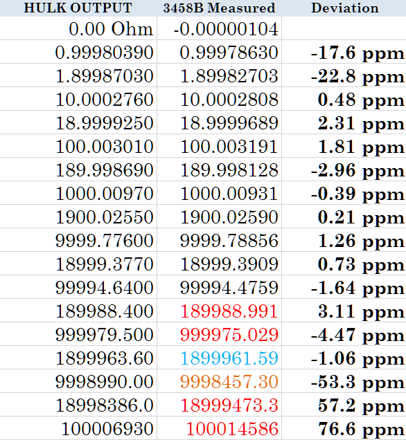
AC Voltage check was completed using Wavetek 4920M AC Voltage Standard
AC Voltage Calibration report, H1 MFC, August 7, 2018
Year 2019
In October 2019 unit was damaged due to M5.4 earthquake. MFC was running 1 ADC range experiment while quake struck, which possibly caused some relays to incorrectly switch and cause crack and physical damage to Z1 thin-film resistor network on A10 resistance PCBA. In November replacement network was installed and unit was recalibrated.
Year 2022
Resistance verification with bridges was performed in April 2022. This experiment was to confirm ACAL values and specifications with typical lab environment operation, such as uncontrolled temperature swings from +22 to +27 °C.
Summary on spent resources
Together with Fluke 5725A Booster amplifier this project took about $20K USD over 2 year period, and so far this was one of the most challenging repairs here. It will be a while till this investment pays for itself, but there are many benefits with 24/7 available 7½ precision calibrator rig for analog design and various experiments.
And everything started with just innocent buy of 5700A A11 PCBA for $200 to tinker with. Who knew that idea to make stand-alone LTFLU reference get converted into this build?
“Volt-nutting” at it’s finest, as even not every calibration lab actually own fully-featured 5720A.
Fortune favors the bold. Perhaps hobbyist with that level of commitment could already buy used and fully working Fluke 5700A, which could need only minor repairs (hopefully). But that was not the goal of this xDevs.com project. It is more interesting to understand (and share via such article) what goes into design of high-performance instrument like Fluke 5700/5720A series multi-function calibrators, with hands-on approach during complex repair tasks.
Getting 24 boards from different random calibrators to work all together in one “Hulk” unit was precisely the ultimate purpose and the prize. xDevs.com will definitely cover more about this “Hulk of metrology” and it’s performance results in future articles and experiments. We also have remote access to other 5700A, 5720A and 5730A for data comparison to perform interesting experiments in 2019.
Discussion about this article and related stuff is very welcome in comment section or at our own IRC-chat server: irc.xdevs.com (standard port 6667, channel: #xDevs.com). Web-interface for access mirrored on this page.
Projects like this are born from passion and a desire to share how things work. Education is the foundation of a healthy society - especially important in today's volatile world. xDevs began as a personal project notepad in Kherson, Ukraine back in 2008 and has grown with support of passionate readers just like you. There are no (and never will be) any ads, sponsors or shareholders behind xDevs.com, just a commitment to inspire and help learning. If you are in a position to help others like us, please consider supporting xDevs.com’s home-country Ukraine in its defense of freedom to speak, freedom to live in peace and freedom to choose their way. You can use official site to support Ukraine – United24 or Help99. Every cent counts.
Modified: Nov. 13, 2023, 10:11 a.m.
References
- EEVBlog : The LTFLU (SZA263) reference thread
- 38hot.net : SZA263 thread (chinese)
- xDevs.com : Fluke 5700A repair worklog
- AN: An Evaluation of Artifact Calibration in the 5700A Multifunction Calibrator
- An evaluation of the 5700A Series II Artifact Calibration
- Thin Film designs for 1000V AC Range resistors in 792A and 5790A
- Fluke 5700A/5720A Series II MFC Service Manual with schematics
- Fluke 5700A MFC Service Manual with schematics
- Siliconix J2908 information page
- KITAGAWA INDUSTRIES America Technology : EMI shielding solutions
- American Zettler relays
- RF Parts supplier
- Nichicon Capacitor replacement sheet
- EZ-Hook wideband N to dual banana adapter


