Contents
- Intro
- Specifications comparison
- Manuals
- Teardown
- Firmware
- Repair workflow
- Calibration
- Testing and performance
- Summary
Intro
While some serious hobbyists, who interested in precision measurements do own DC voltage standards such as Fluke 732A/732B, resistance standards like Fluke 5450A, Fluke 742 , very few of them have high-end multi-function calibrators. These instruments are usually cost many thousands of dollars and calibration fees often also at prohibitive price for most of hobby labs. Viable alternative to Datron 4800 series multi-function calibrators (MFC) or modern Fluke 5500A / 5700A / 5720A are old obsolete Fluke 5440B or Datron 4700 series units, which are still available from time to time on secondary market for approachable prices. These calibrators are worthy option if one have multiple 6½-digit+ DMMs and sources, which often require wide variety of stable voltages, currents and resistance levels for calibration purposes.
And since we currently have no less than four 7½-digit Keithley Model 2001, two 8½-digit Keithley 2002, one HP 3458A and few other instruments, getting broken calibrator for repair and future use can be a useful investment. Official calibration by Tektronix service for just one Keithley 2001 is priced at $550 USD tag, making support and maintenance of 1 year interval rather expensive.
So when I saw this “unknown” Time Electronics Model 9823 AC-DC calibrator, and checking specification sheet, it was hard to resist than bid button. Let’s see what we get ourselves into.

Specifications comparison
Discontinued Time Electronics Model 9823 specified to be 10ppm/year accurate, with 6½-digit display, self-test function, and AC frequency ranges up to 20kHz. There are also cheaper Model 9822 (30ppm/year, 6½-digit display) and Model 9821 (100ppm/year, 4½-digit display) units. All three today are discontinued and replaced by Time Electronics 5025C (15ppm/year).
| Description | Time Electronics Model 9823 | Fluke 5500A | Fluke 5720A | Datron 4808 |
|---|---|---|---|---|
| Voltage ranges, DCV | 20mV,200mV,2V, 20V,200V, 1kV | 330mV,3.3V,33V,330V,1020V | 220mV,2.2V,11V,22V,220V,1100V | 100µV,1mV,10mV,100mV,1V,10V,100V,1000V |
| Accuracy 24 hour, ppm | 4+2, 3+2, 1+1,1+1,10+10,10+10 | 5, 4, 4, 4.5, 4.5 | 4+0.4,3+0.7,2+2.5,2+4,3+40,4+400 | 2+1u,2+0.5,1+0.5,2+0.5 |
| Accuracy 90 day, ppm | 5+2, 5+2, 5+2,5+2,20+10,20+15 | 50, 40, 40, 45, 45 | 6+0.4,3.5+0.7,2.5+2.5,2.5+4,3.5+40,4.5+400 | 15+1µV / 15+1 |
| Accuracy 1 year, ppm | 10+2, 10+2,10+2,10+2,30+10,30+15 | 60, 50, 50, 55, 55 | 7.5+0.4,5+0.7,3.5+2.5,3.5+4,5+40,6.5+400 | 35+5µV / 35+5 |
| Tempco, ppm/°C | 4 , 3 , 2, 2, 4, 4 | 0.4,0.3,0.15,0.2,0.3,0.5 | 2,2,2,2,1.5,1,1.5,2 | |
| Voltage ranges, ACV | 20mV,200mV,2V,20V,200V,1kV | 33mV,330mV,3.3V,33V,330V,1020V | 2.2mV,22mV,220mV,2.2V,22V,220V,1100V | 1mV,10mV,100mV,1V,10V,100V,1000V |
| Accuracy 24 hour, ppm | 80+50(<1k),200+200(<2k),500+300(<20k) | 1+1,1+1,10+10,10+10 | 70+4 (<20k) ... 2400+20 (<1M) | 170+10(<31Hz), 80+10(<100k) |
| Accuracy 90 day, ppm | 200+50, 600+200, 2500+500 | 300+60, 250+60, 800+80 | ||
| Accuracy 1 year, ppm | 300+50, 800+200, 4000+500 | 400+60, 300+60, 0.1%+80 | ||
| Tempco, ppm/°C | 15 | 10, 6, 10 | ||
| Current ranges, DCI | 200µA,2mA,20mA,200mA,2A,10A | 3.3mA,33mA,330mA,2.2A,11A | 220µA,2.2mA,22mA,220mA,2.2A | 100µA,1mA,10mA,100mA,1A,10A |
| Accuracy 24 hour, ppm | 10+5, 10+5,10+5,10+5,25+20,200+200 | 35+8, 35+8, 35+8, 45+0.8, 60+25 | 15+10, 15+15, 30+15 | |
| Accuracy 90 day, ppm | 30+10,30+10,30+10,30+10,60+30,400+300 | 40+8, 40+8, 40+8, 50+0.8, 65+25 | 50+15, 115+20, 150+25 | |
| Accuracy 1 year, ppm | 50+10,50+10,50+10,50+10,100+30,700+300 | 50+8, 50+8, 50+8, 60+0.8, 80+25 | 115+20, 250+30, 300+30 | |
| Tempco, ppm/°C | 8 , 8 , 8, 8, 15, 30 | 30, 12, 12, 12, 30, 30 | ||
| Current ranges, DCA (20Hz-1kHz) | 200µA,2mA,20mA,200mA,2A,10A | 330µA,3.3mA,33mA,330mA,2.2A,11A | 220µA,2.2mA,22mA,220mA,2.2A | 100µA,1mA,10mA,100mA,1A,10A |
| Accuracy 24 hour, ppm | 100+30 (<200mA), 200+50, 400+200 | |||
| Accuracy 90 day, ppm | 300+100 (<200mA), 350+100, 700+300 | |||
| Accuracy 1 year, ppm | 400+100 (<200mA), 500+100, 1000+300 | |||
| Tempco, ppm/°C | 20 (<200mA), 30, 50 | 20, 40, 70, 150 | ||
| Resistance | 10Ω,100Ω,1KΩ,10KΩ,100KΩ,1MΩ,10MΩ | 0 to 330MΩ synth | 0Ω to 100MΩ in 1.0x and 1.9x steps | 10Ω,100Ω,1KΩ,10KΩ,100KΩ,1MΩ,10MΩ,100MΩ |
| Accuracy 90 day, ppm | 20, 10, 8, 8, 8, 20, 50 | 70ppm – 4000ppm | 40µΩ, 80ppm, 9ppm, 7.5ppm, 31ppm, 95ppm | 30,6,6,6,6,25,100,125 |
| Accuracy 1 year, ppm | 50, 20, 20, 20, 25, 60, 100 | 120ppm – 5000ppm | 40µΩ, 95ppm, 10ppm, 8.5ppm, 40ppm, 100ppm | 75,20,20,20,25,60,200,500 |
| Tempco, ppm/°C | 5, 4, 3, 3, 3, 3, 5 | 4,6,2,2,2,2,2,2,2,2,2,2,2.5,3,5,8,12 | 6,2,2,2,2,6,10,20 | |
| Dimensions | 3U 19” standard rack-mount, 17kg | 4U 19” standard rackmount, 36kg | ||
| MSRP (February 2016) | Obsolete unit | $24900 | $32000 USD | $15000 USD used |
This beast is made in 1988, but was “recently” tested in 2004 by Time Electronics and in March 2006 by Absolute Calibration in UK.
Manuals
Technical Manual 9823, Version 2.1, Part 1
Technical Manual 9823, Version 2.1, Part 2
Technical Manual 9823, Version 2.1, Part 3
Teardown and circuit overview
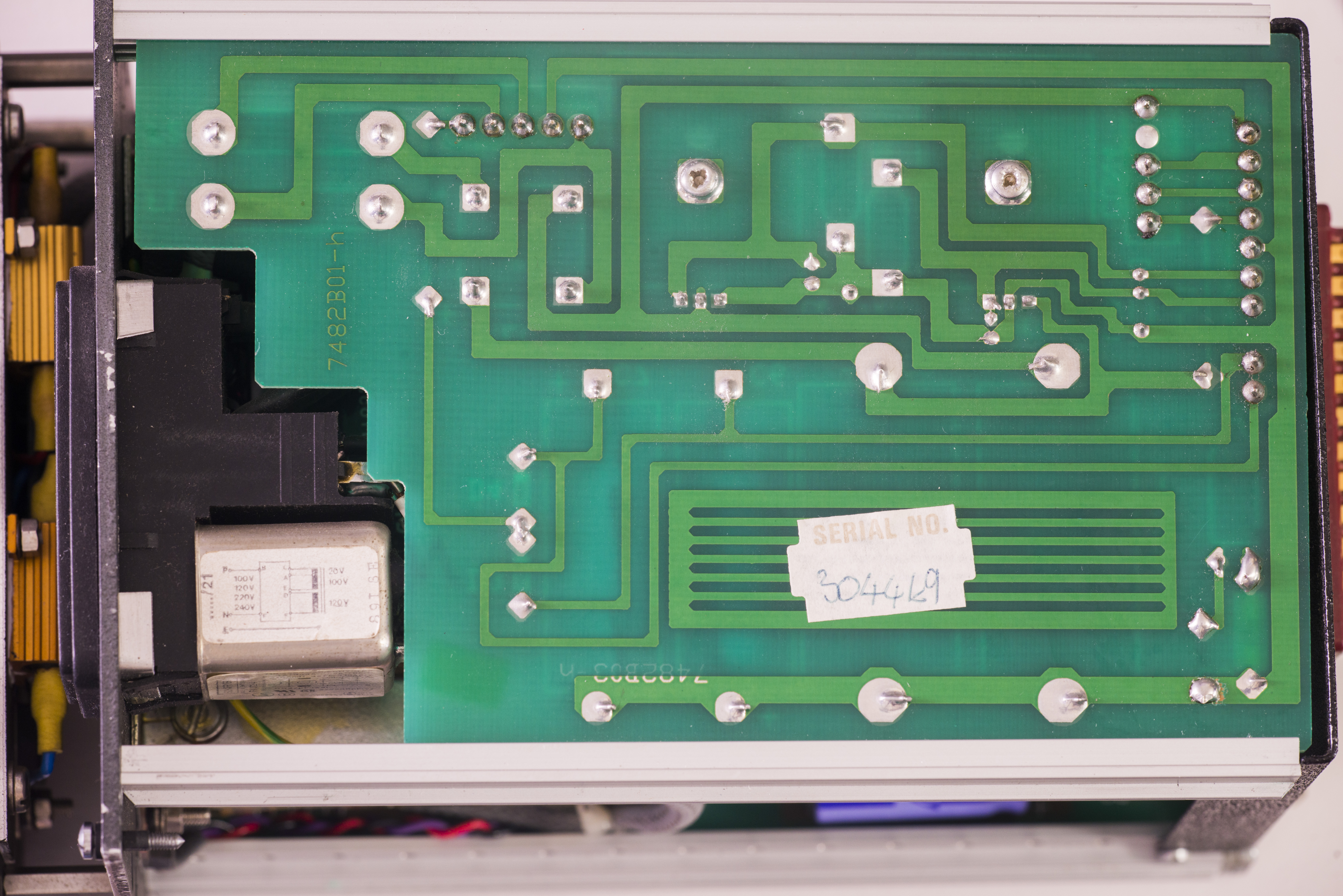
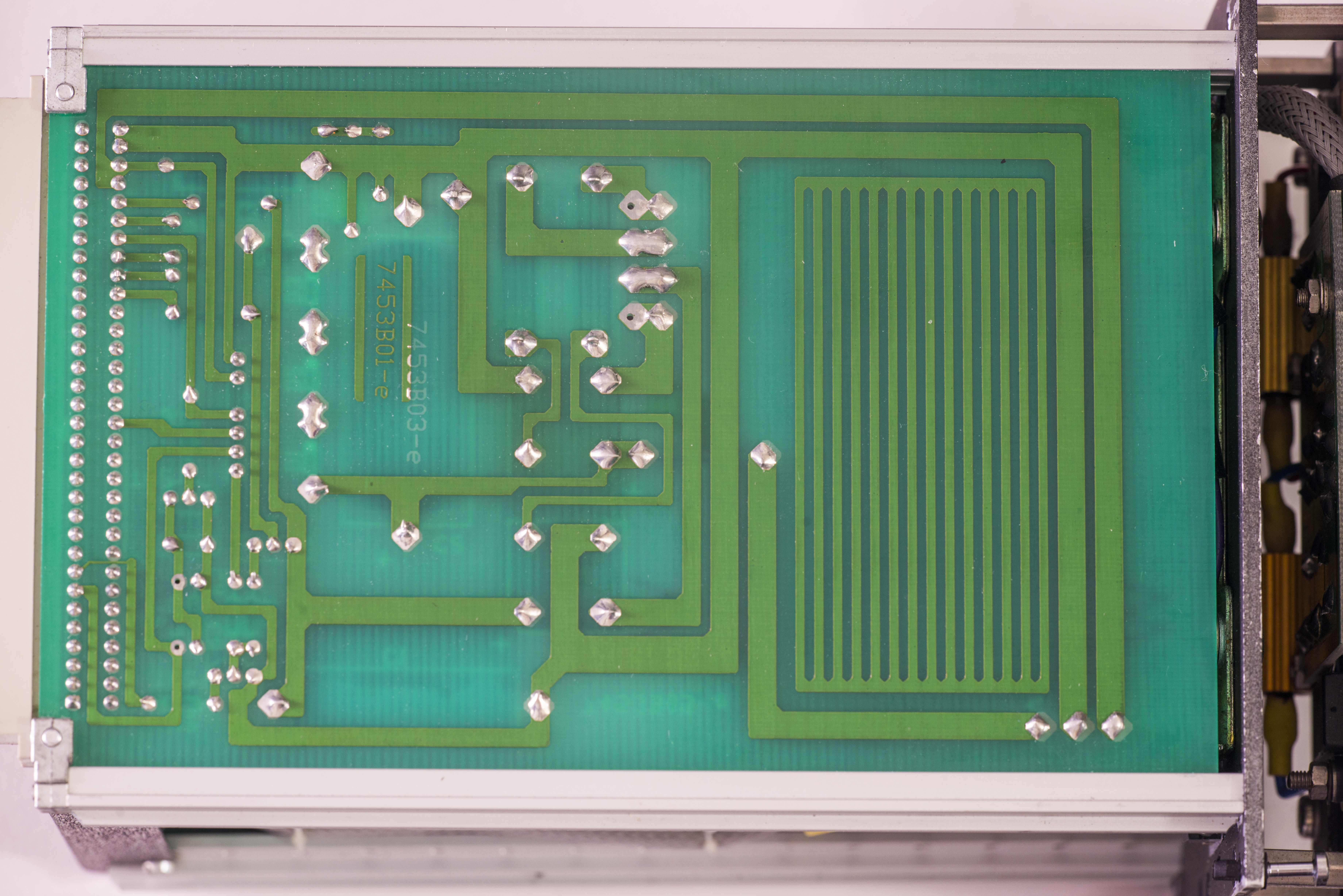
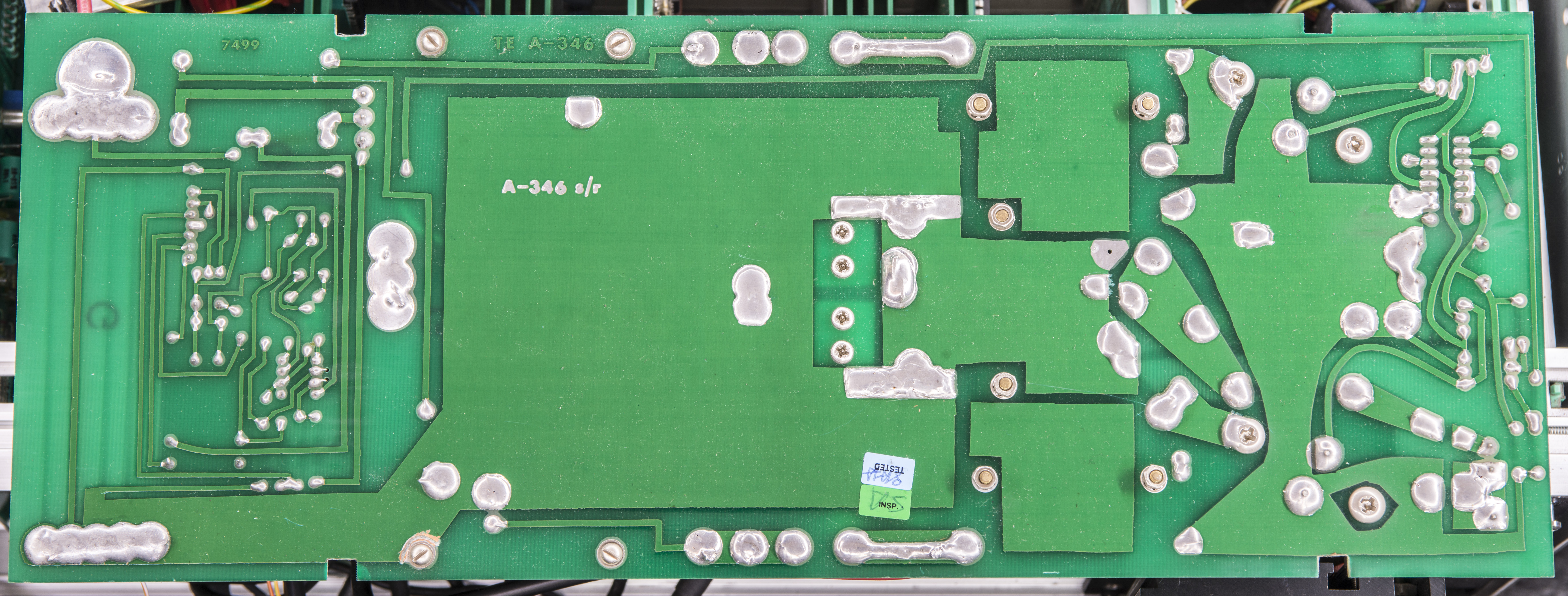
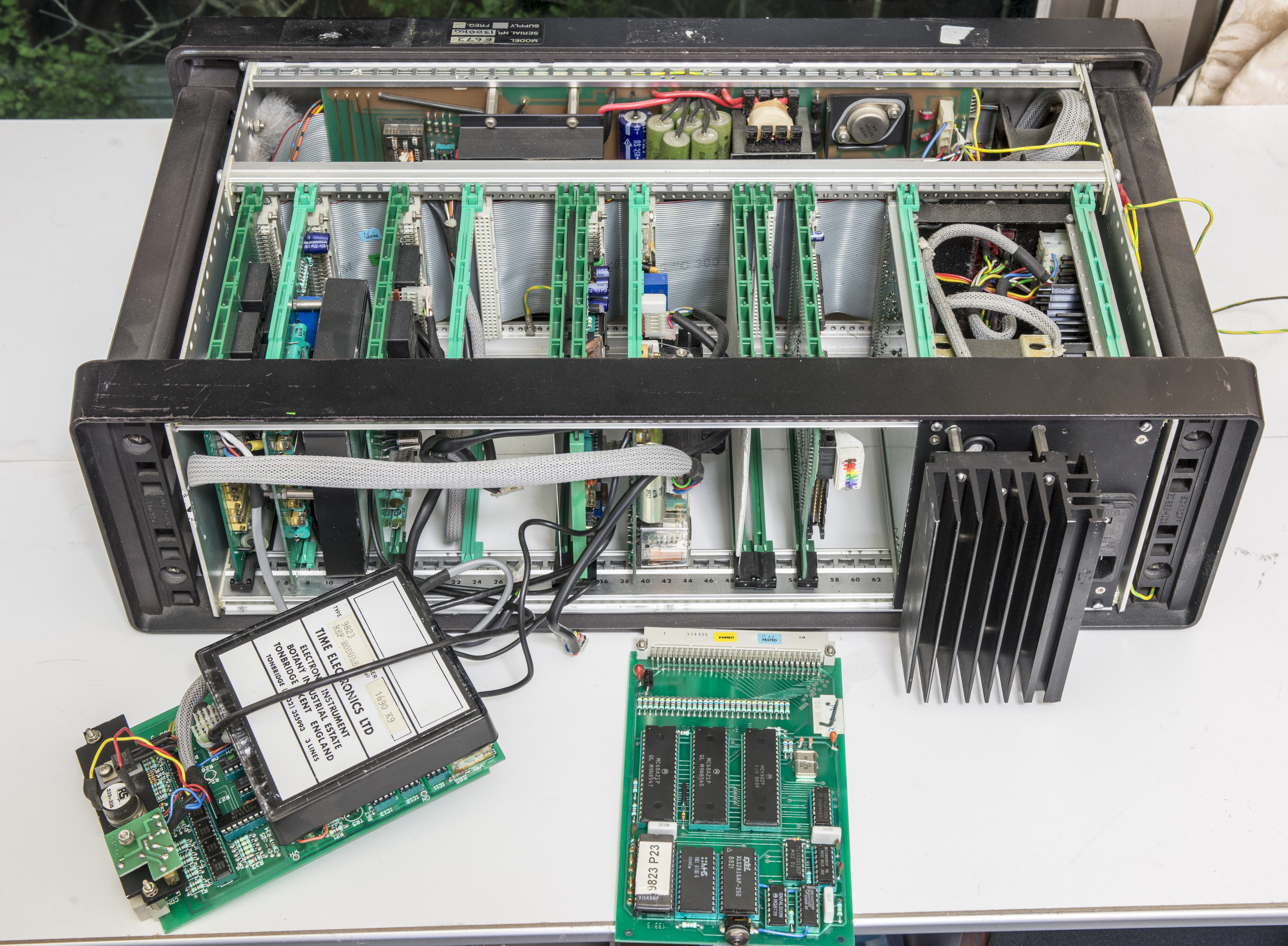
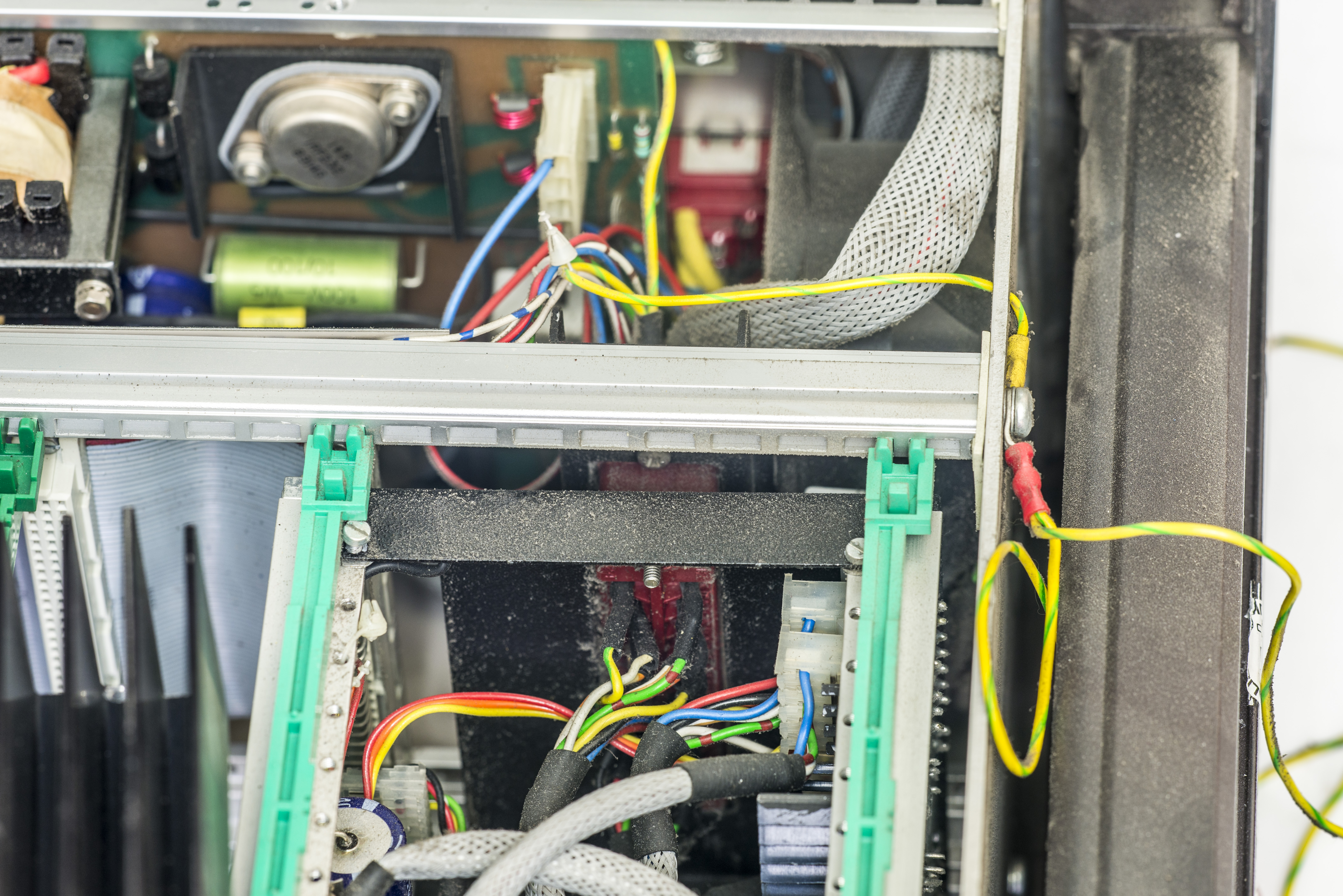
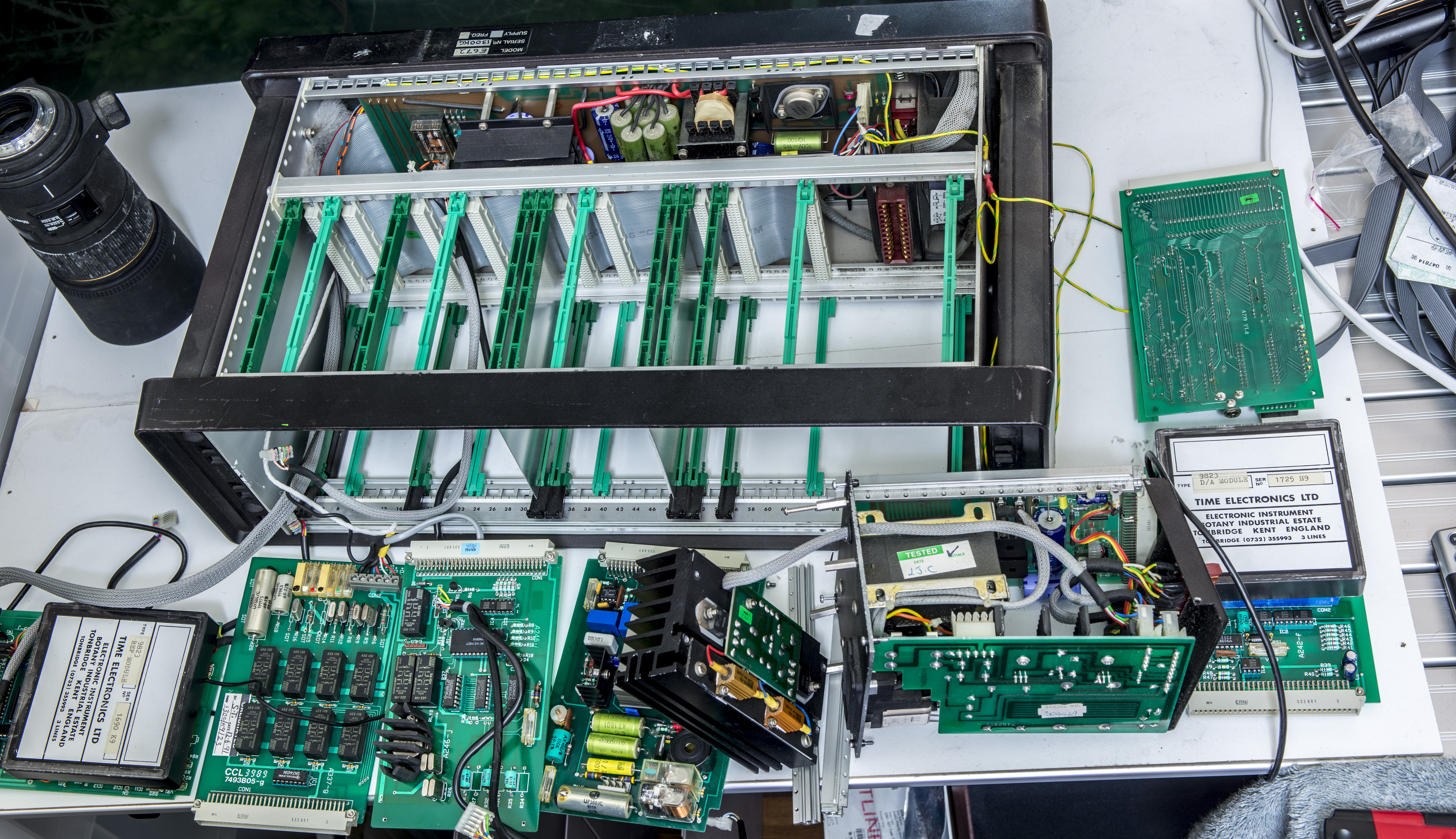
Calibrator is fitted in standard Eurocard 19” 3U rack, such as this made of aluminum frame panels and extruded bars. Outer black cast frame is easily removable, with unit sliding from front face. Various modules are made using standard 3U card type, installed into frame from rear side.
Backplane interconnection performed via ribbon cable with male connectors spaced to mate with cards. Large 110/220VAC fan located on the side provide cooling for high-current power supply/assembly at front side of calibrator frame. All modules and PCBs connect to 64-way signal bus via DIN 41612 type connector.
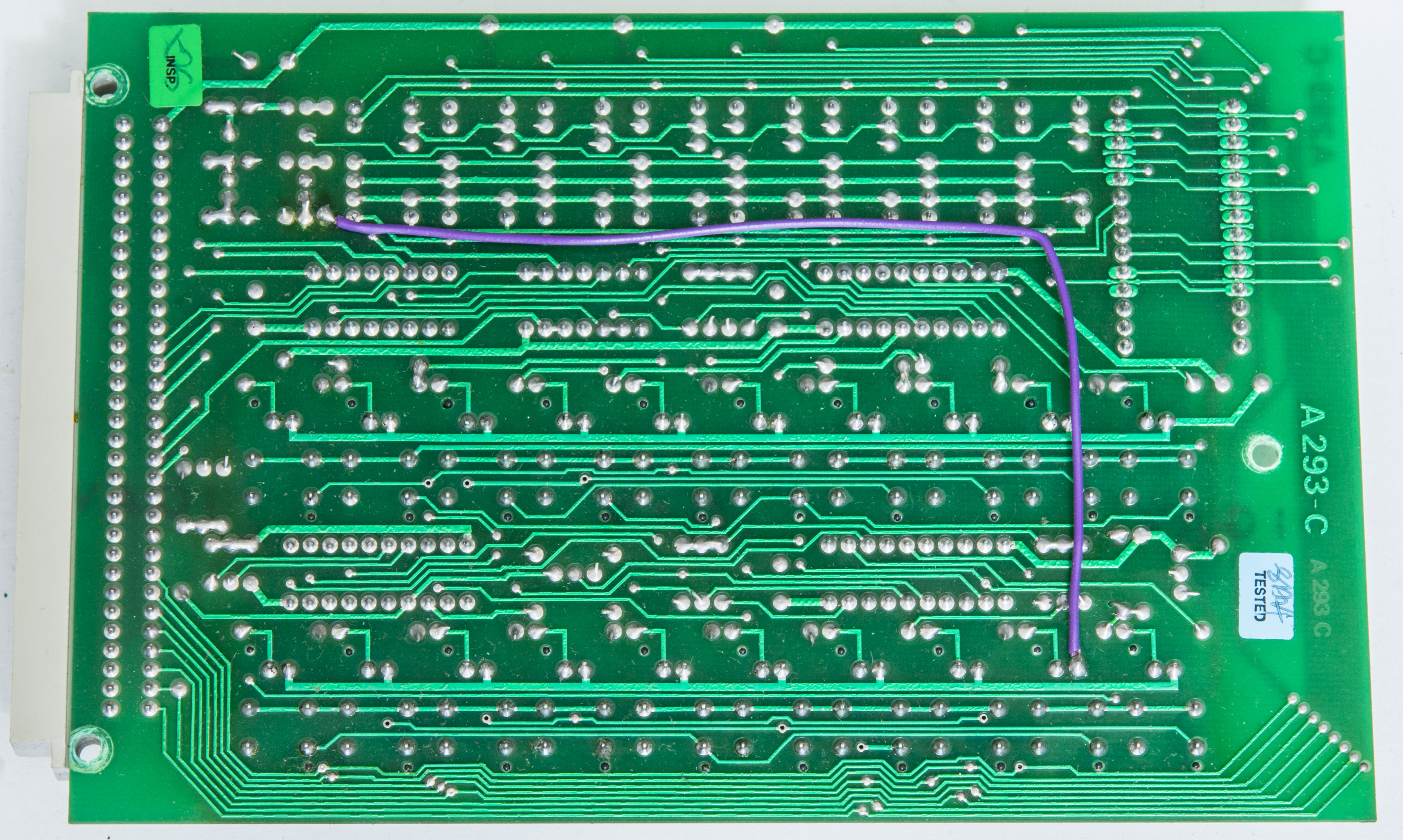
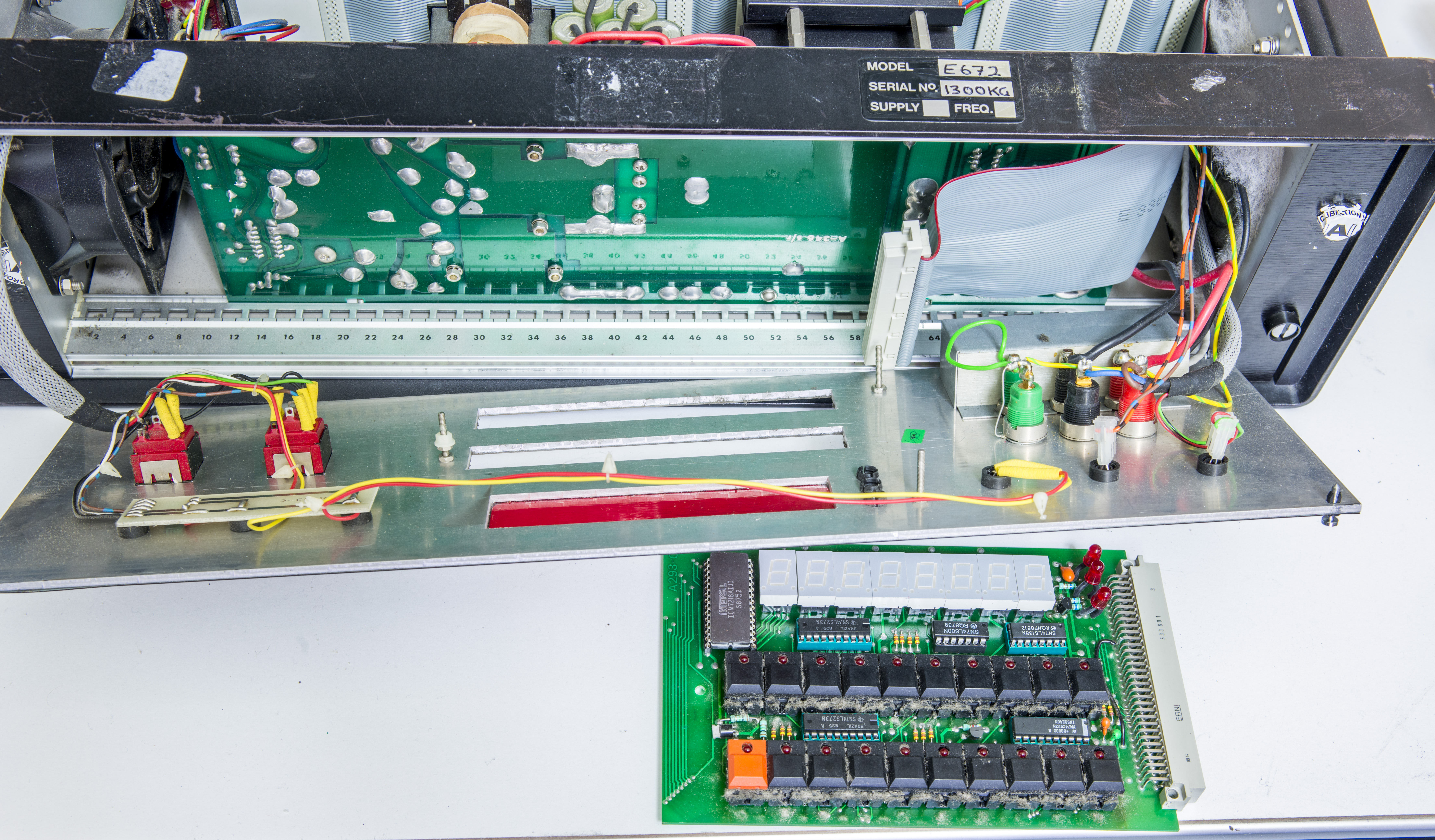
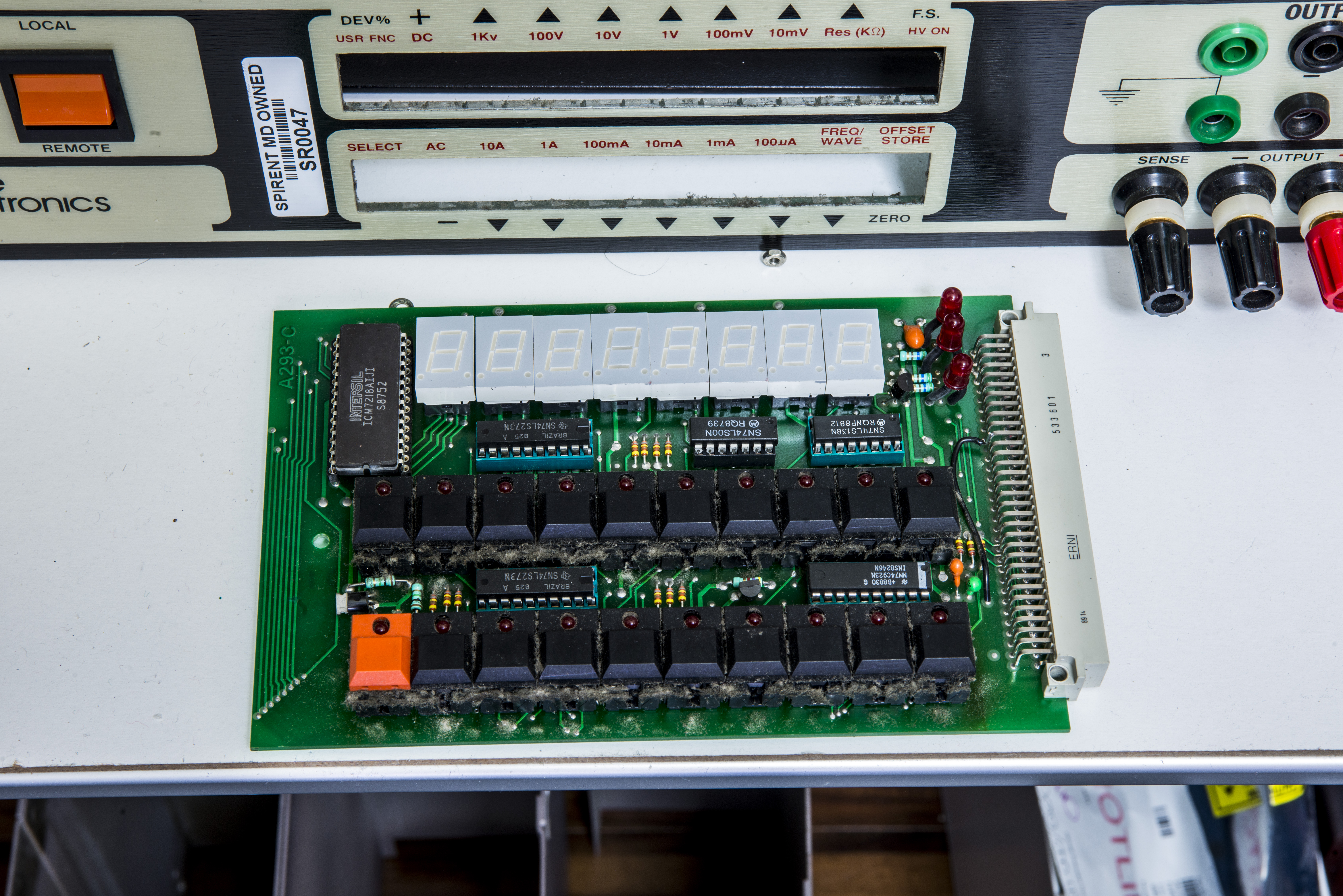
Front-panel assembly, A293-C
Front panel easily removed by releasing four captive screws on corners and lifting it from the frame.
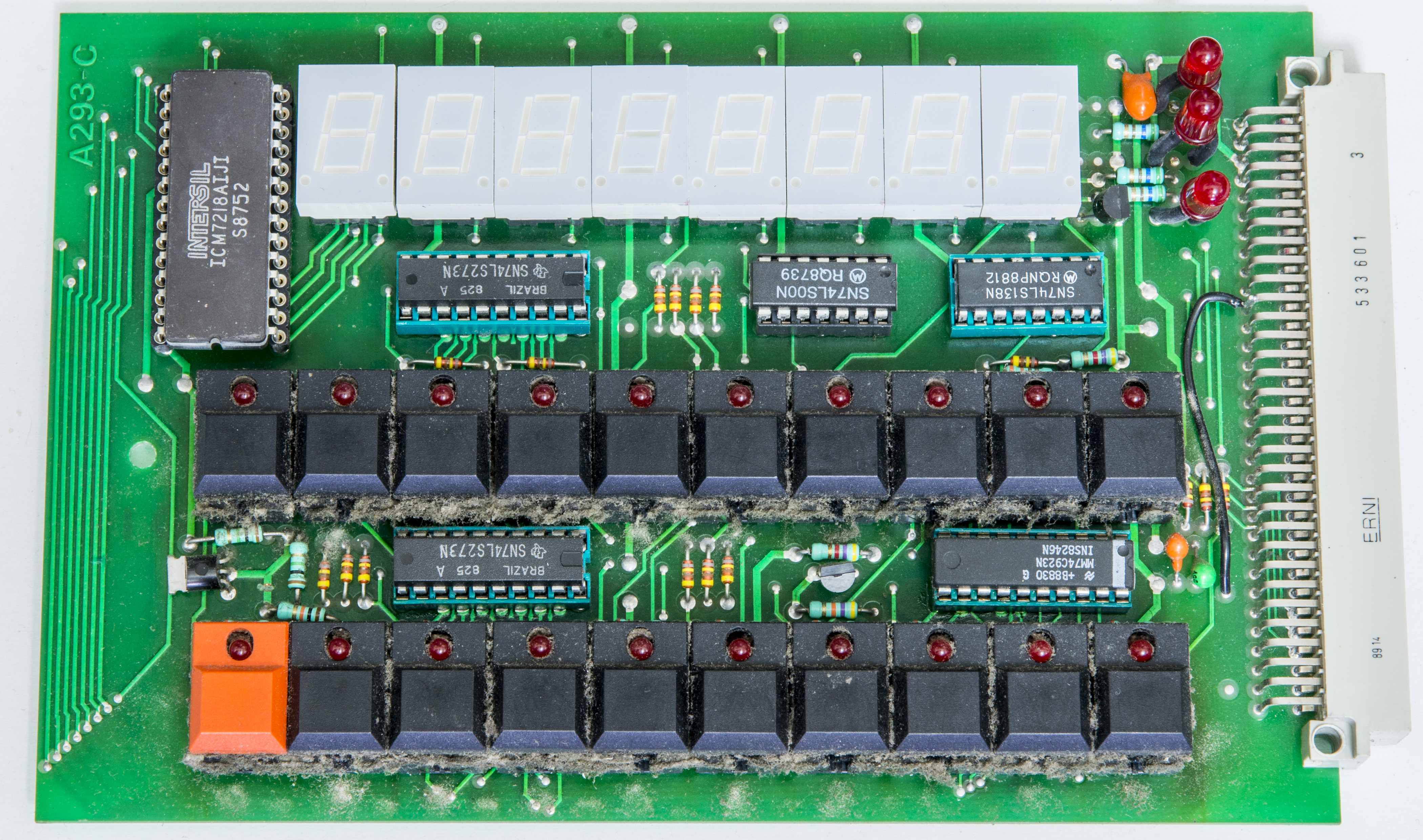
LED 7-segment display is controlled by Intersil ICM7218, which is 8-digit LED microprocessor-compatible multiplexed display decoder driver. It’s 5V logic chip, capable of driving segments at 40mA, with 250Hz scan rate.
Few other 74-series logic chips are in charge of LEDs. Obscure MM74C923N is a 20-Key encoder to convert button actuation into digital code. Buttons are made of good quality tactile micro-switches with lever cap with nice clicky feel. Board have few bodge wires and traces cut. Address decoding from the bus data is done with help of 74LS138 and 7400 logic.
LED displays are made by HP, HDSP-3730.
Main gold-plated copper binding posts are covered with steel shield.
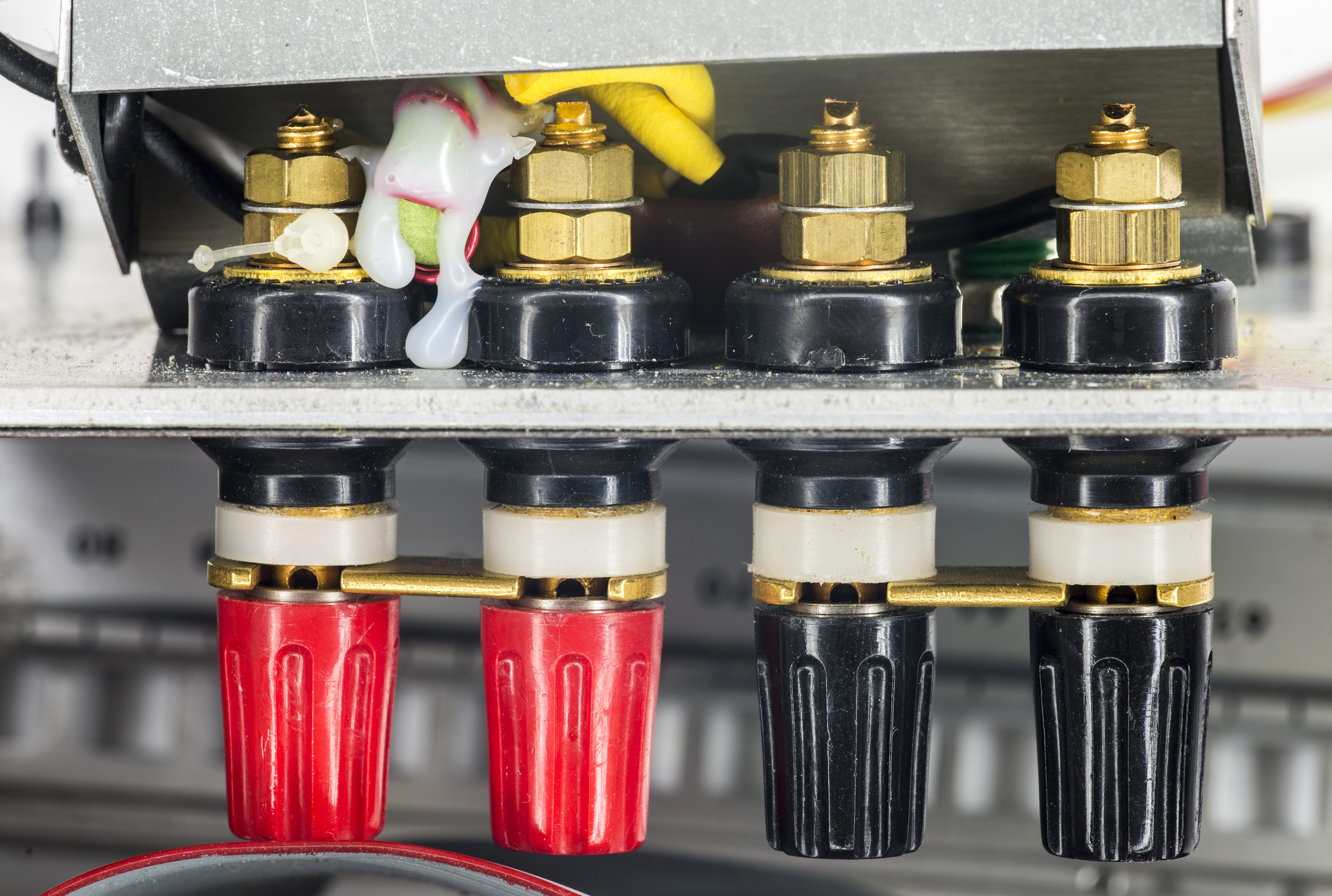
High-voltage 200V and 1000V outputs, as well as high-current 10A have separate output terminals for additional safety. So user will not get dangerous output, unless specifically change output connection to device under test. Also there is 3 second delay and loud beeping will be present once high-voltage/high-current ranges are selected. If output connections are incorrect (for example trying to output current into high-impedance load) front panel display will display error message OP ERROR.
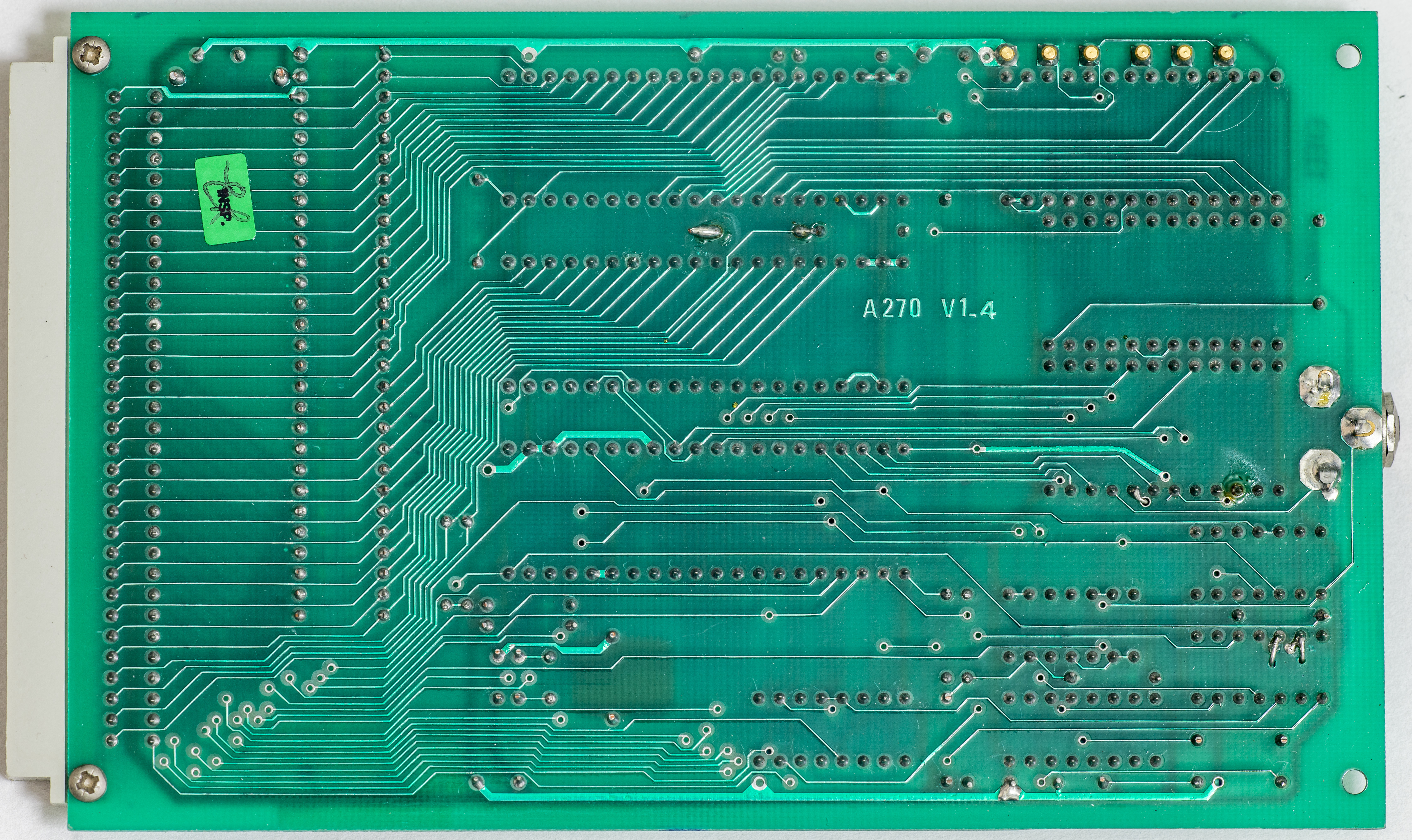
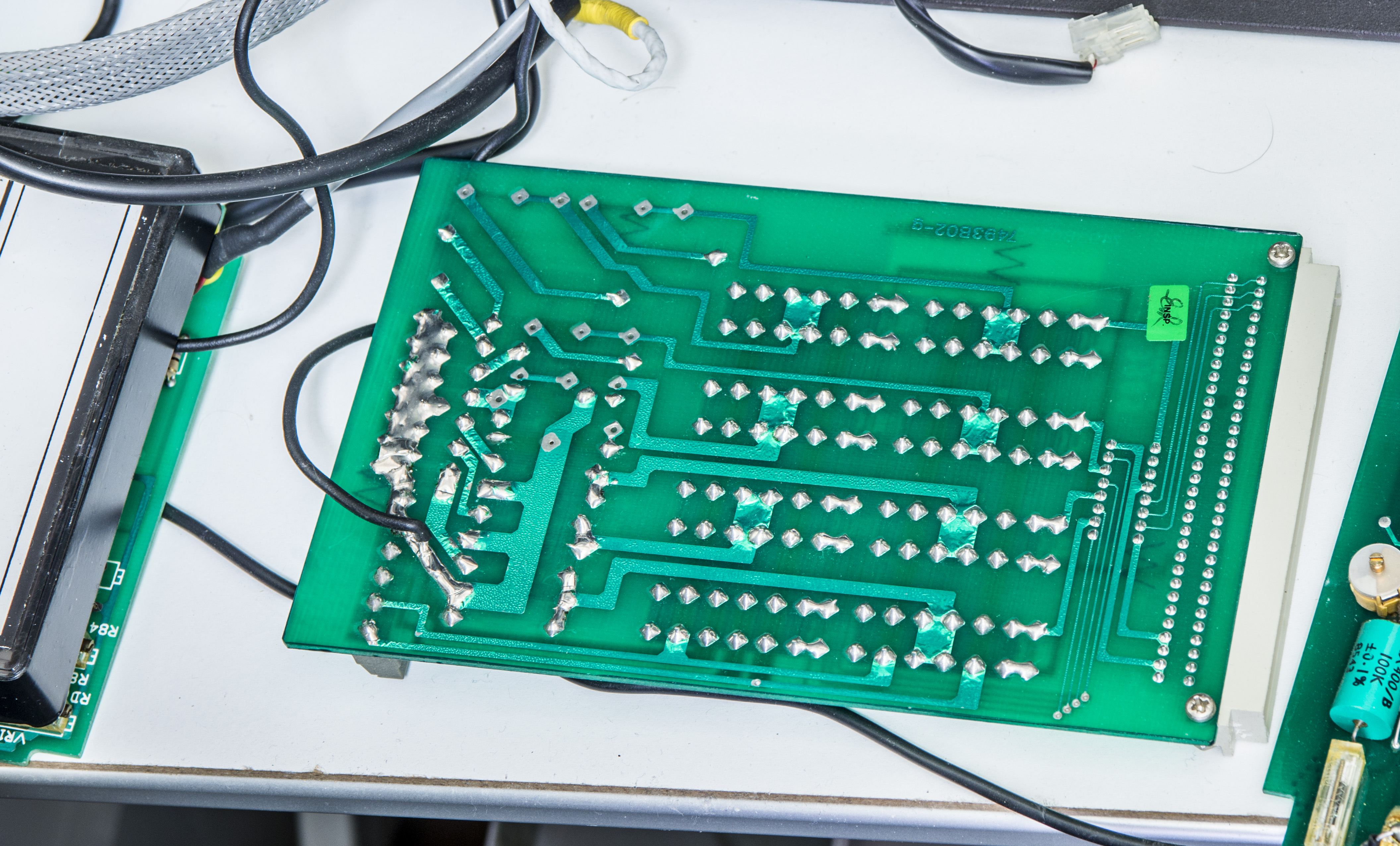
Main processor module, A270 V1.4

This is where digital brain of the instrument reside. Good old friend, Motorola MC6802 8-bit processor is in charge. It does have internal 1MHz clock oscillator and 128 bytes of RAM and have 16-bit memory address bus. Two Motorola MC6821 Peripheral Interface Adapter chips provide GPIO function for the rest of the instrument, with 32 I/O signals on each IC.
Onboard jumper links are provided for using either 16K (2516), 32K (2532) or 64K (2764) PROM options.
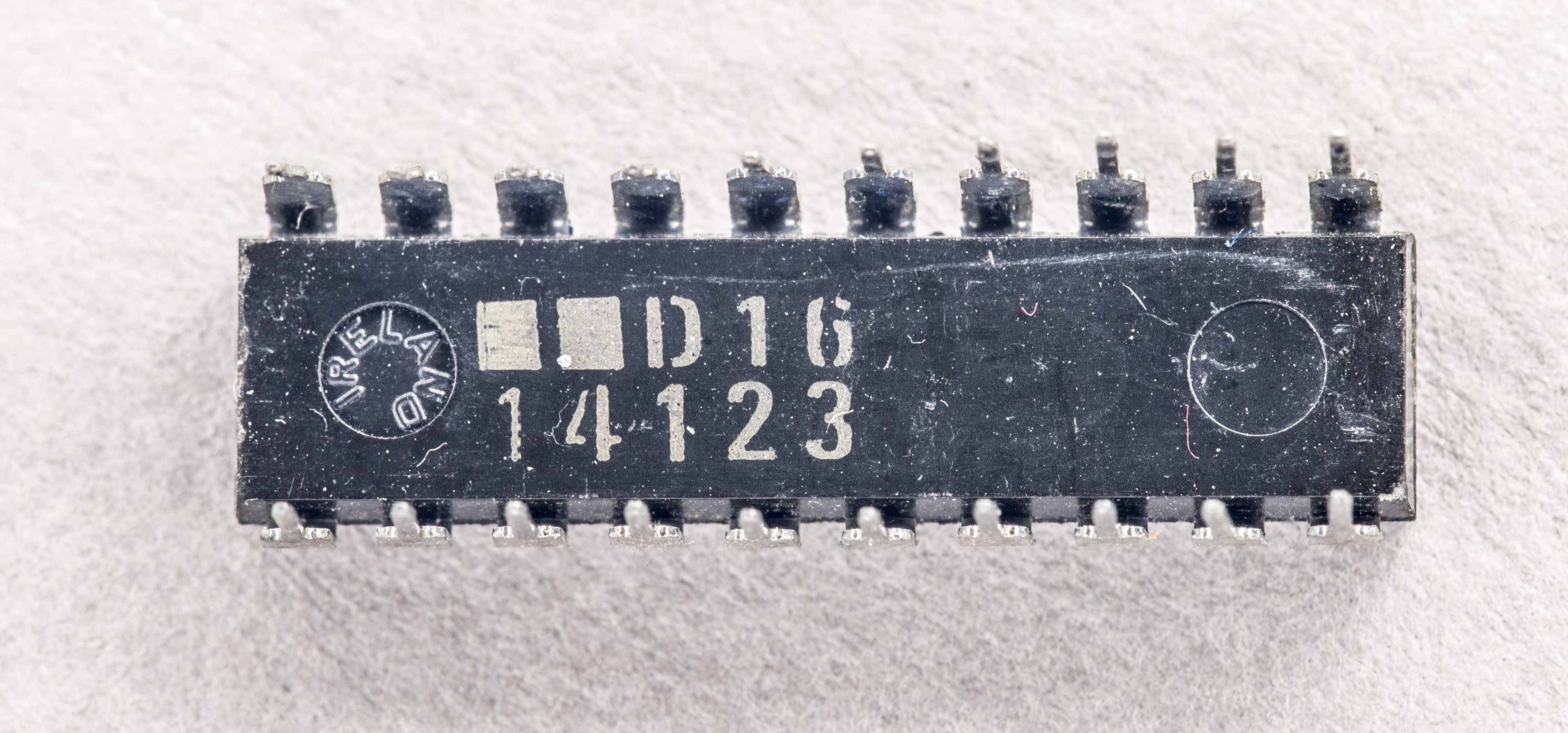
Main firmware of the instrument stored in AM2764A UV-erasable EPROM with label 9823 P23. P23 likely meaning version number here. Right next to it is JEDEC-standard SRAM, MHS MH3-6116L-5 and EXEL XLS2816AP-250 EEPROM for calibration data storage. I had read dumps (available in firmware section) and tested these chips. They confirmed to be OK.
Input jack near calibration ROM is designed for calibration “key” to allow calibration data write. It’s just 3.5mm jack type, so should be easy to bypass later, when we decide to do instrument calibration.
There are few usual 74-series logic ICs and few more unusual packages, such as MC14040B 12-bit binary counter and MC14001B Quad 2-input NOR Gate in bottom corner of processor board.
IEEE-488 GPIB interface assembly – A260-e
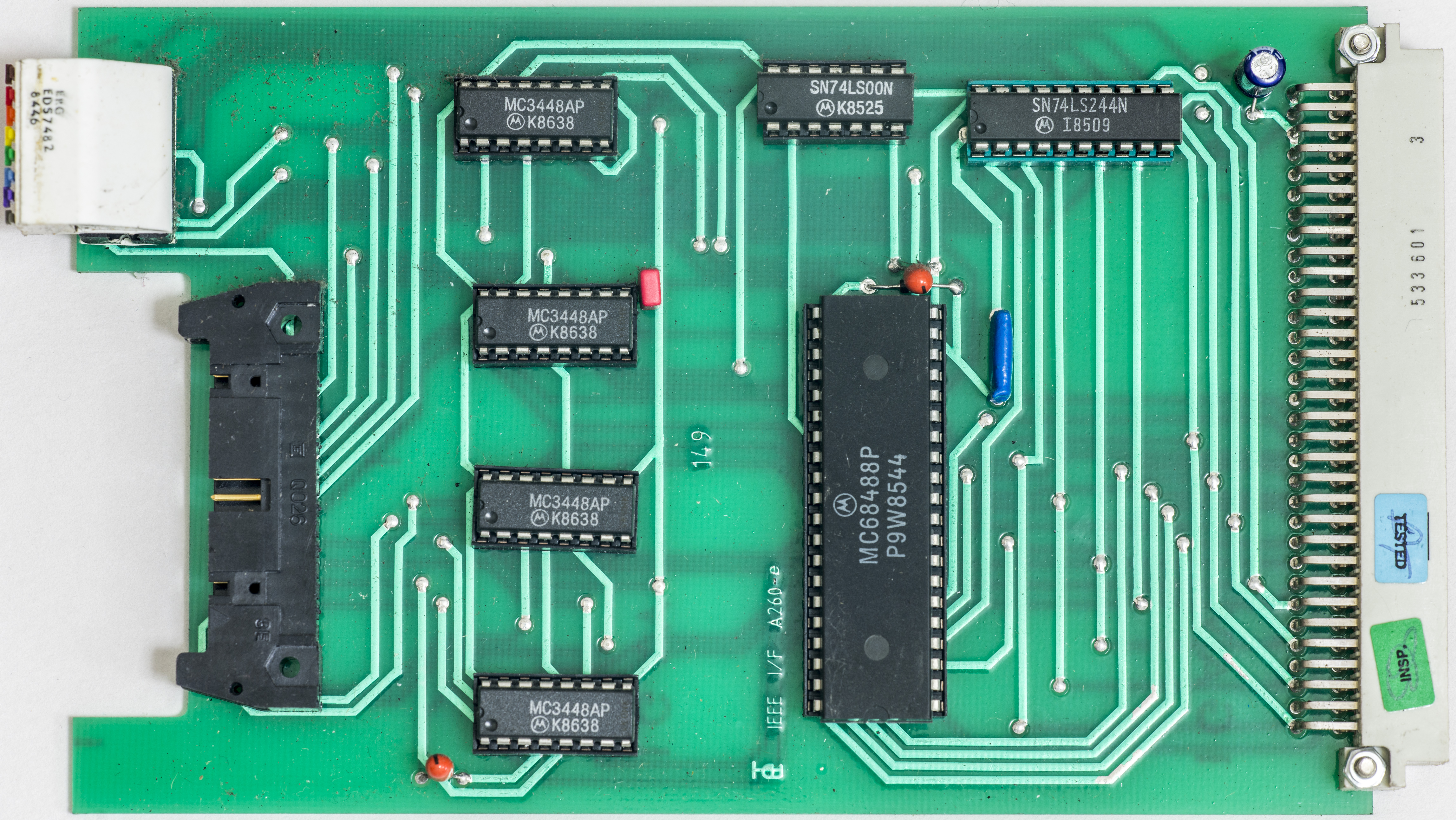
GPIB interface controller is rather simple board, with MC68488 GPIB interface controller for M6800 Motorola MPU processor family and four more MC3448A GPIB transceivers. Couple more 74-series logic packages doing some minor glue function.
It is likely desiged just as reference block diagram:
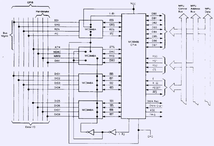
Address select switches are sampled onto 6802 data bus via 74LS244 tristate buffer on instrument power on.
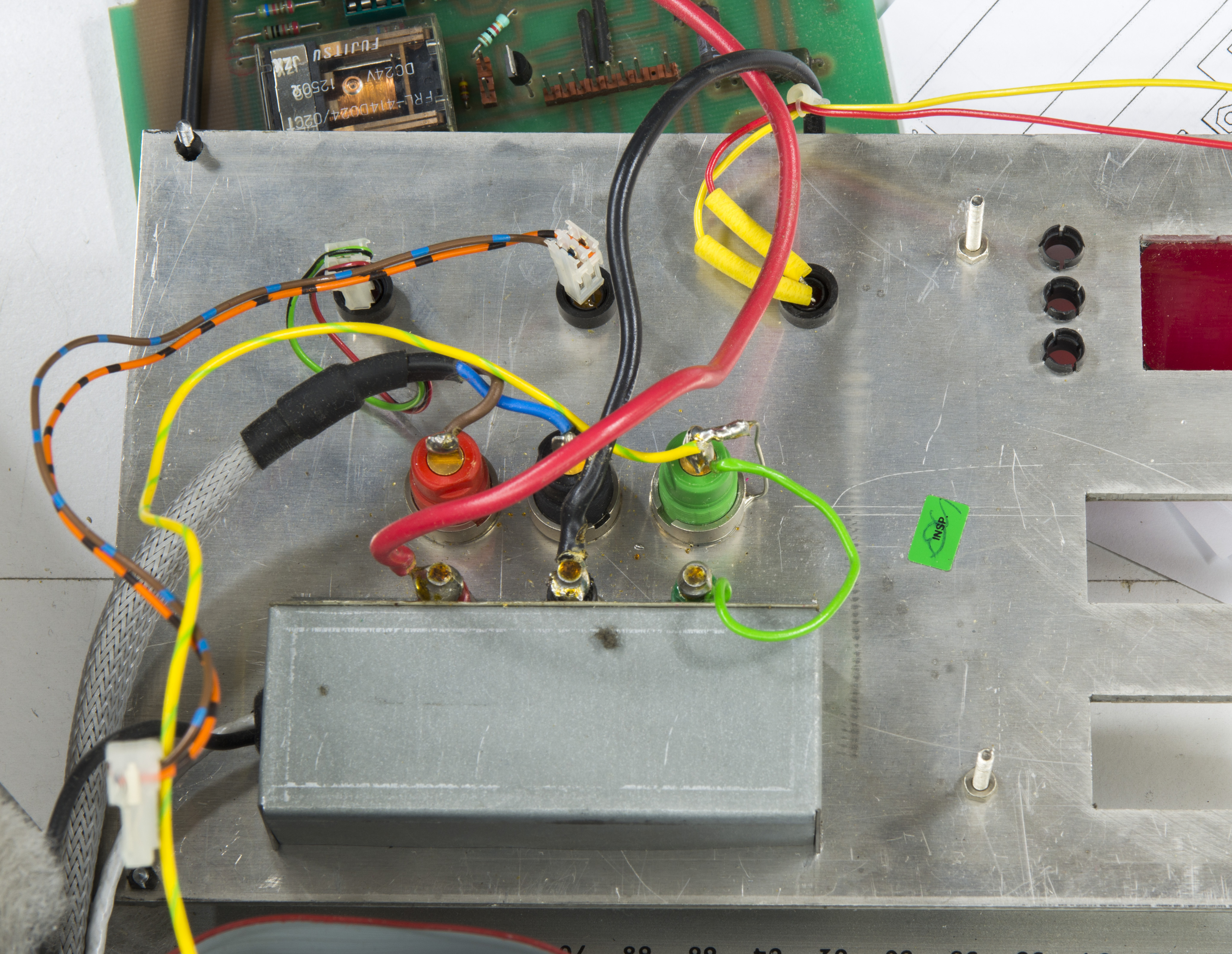
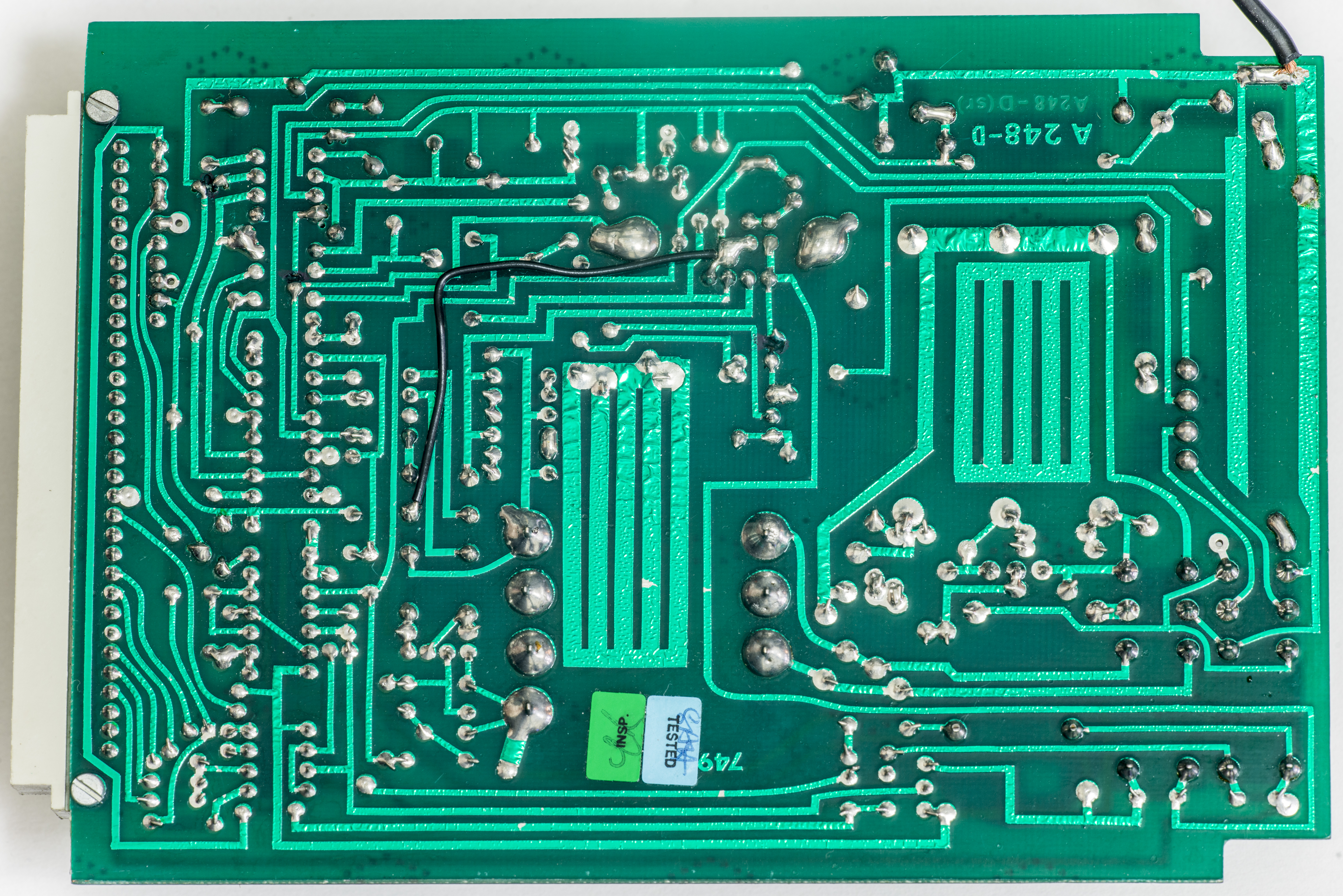
Secondary H.V. power supply – A248-d
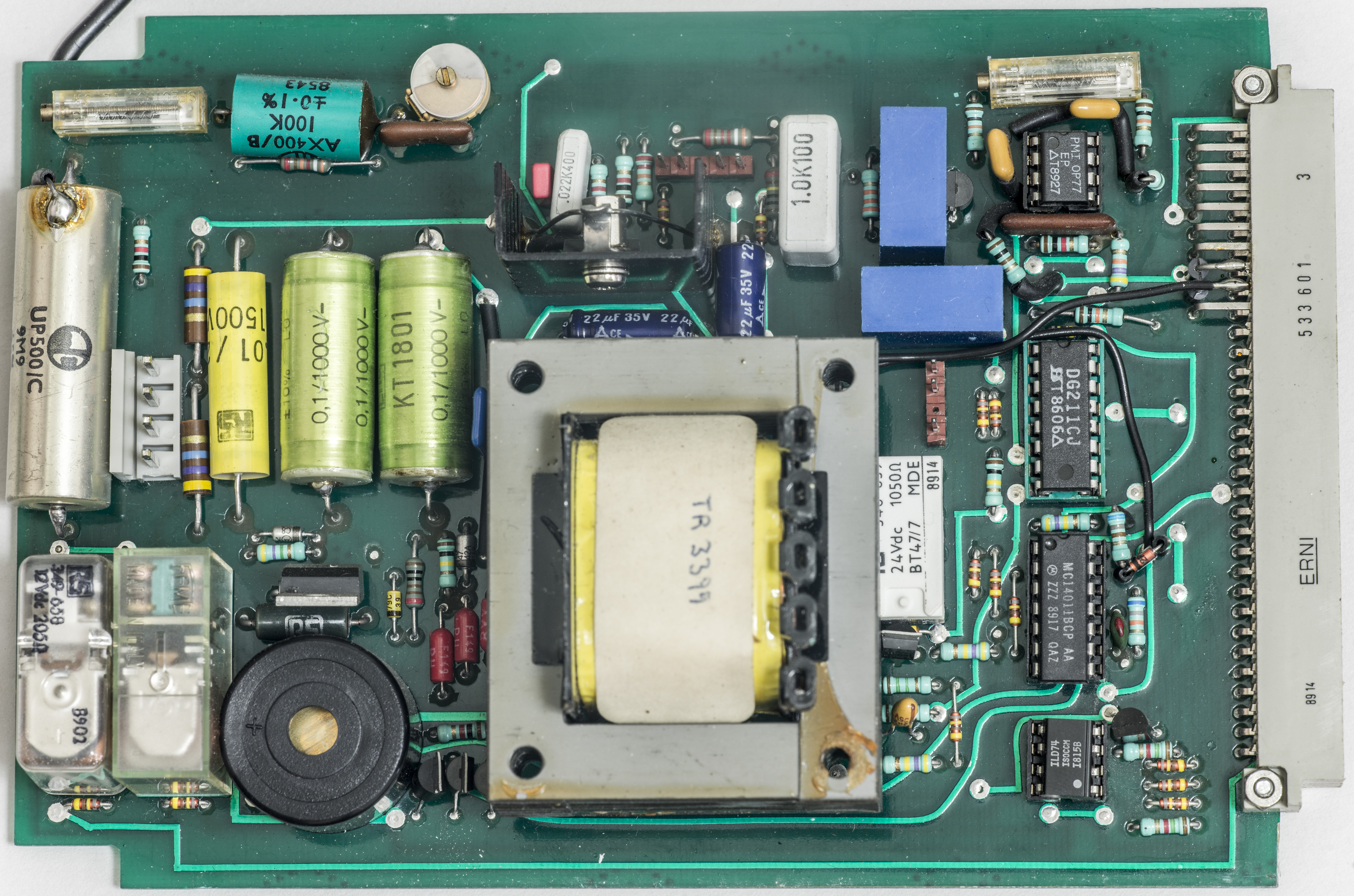
High-voltage divider build using pair of ultra-stable resistors, 100KΩ ±0.1% 5ppm/°C AX400/B wire-wound resistors and 9.9MΩ ±0.5% 3ppm/°C UP500/C. High-value resistor metal case is soldered to board with separate wire, likely to provide guarding for inner resistive element and reduce noise from leakage pickup.
These two resistors divide 0-1000V output down to 0-10V, which is further compared with DAC output voltage to regulate high voltage output.
E-core transformer in center used to convert voltage. Few more parts located near backplane connector, such as operational amplifier OP77 and MC14011 Quad 2?Input NAND Gate. Few relays used for range switching.
Trimpot at board corner is used to adjust high voltage gain of supply unit. There is also a buzzer to alarm user when high-voltage output is operating.
There are two connectors for cables.
3-pin cable wiring connection table:
| Pin | Signal name | Wire color/cable |
|---|---|---|
| 1 | ? | Red on PE white cable |
| 2 | ? | White on PE white cable |
| 3 | None | No pin, key |
| 4 | ? | Blue on gray cable |
4-pin cable wiring connection table
| Pin | Signal name | Wire color/cable |
|---|---|---|
| 1 | ? | Red on PE white cable |
| 2 | ? | White on PE white cable |
| 3 | None | No pin, key |
| 4 | ? | Blue on gray cable |
| 5 | ? | ? |
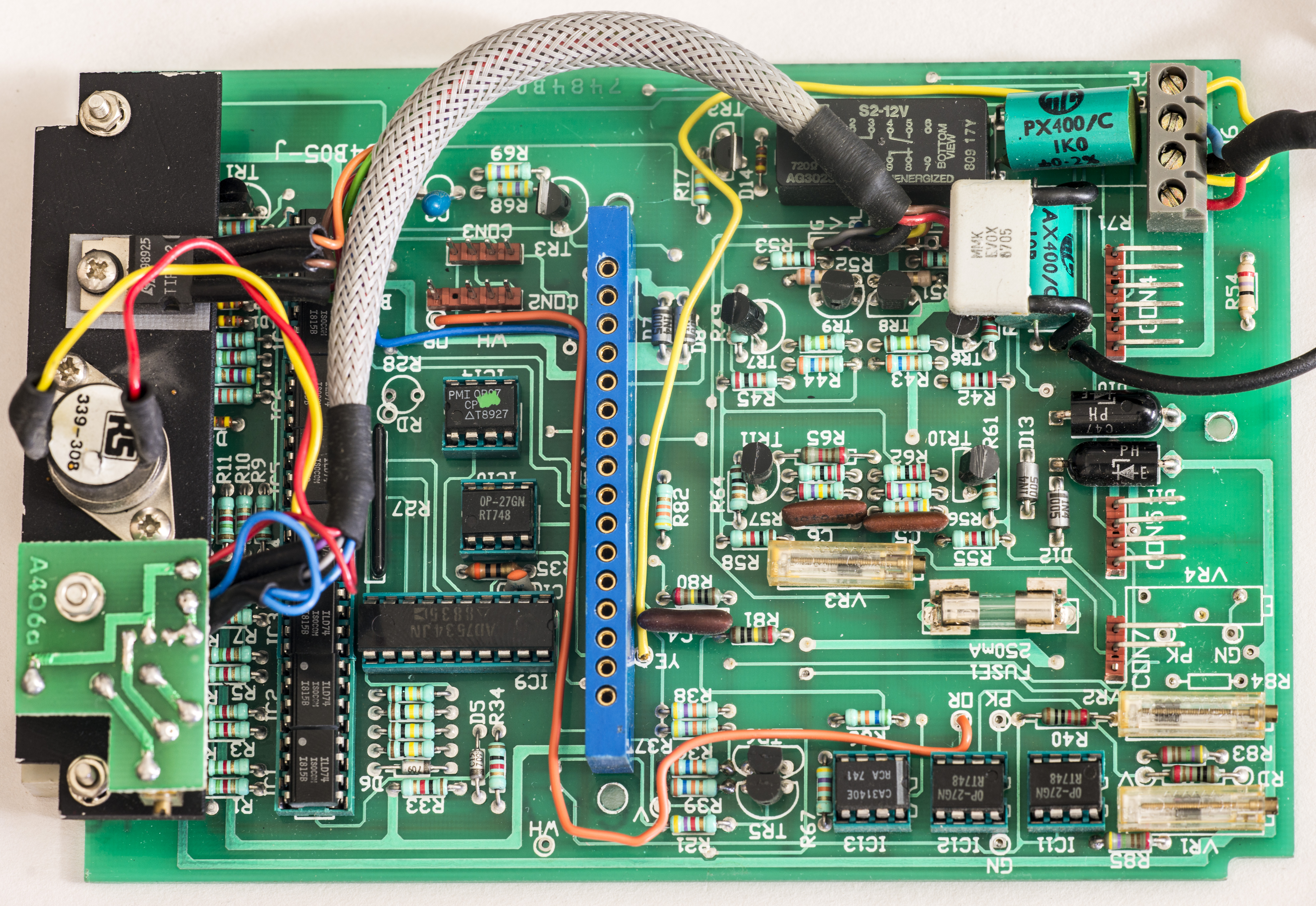
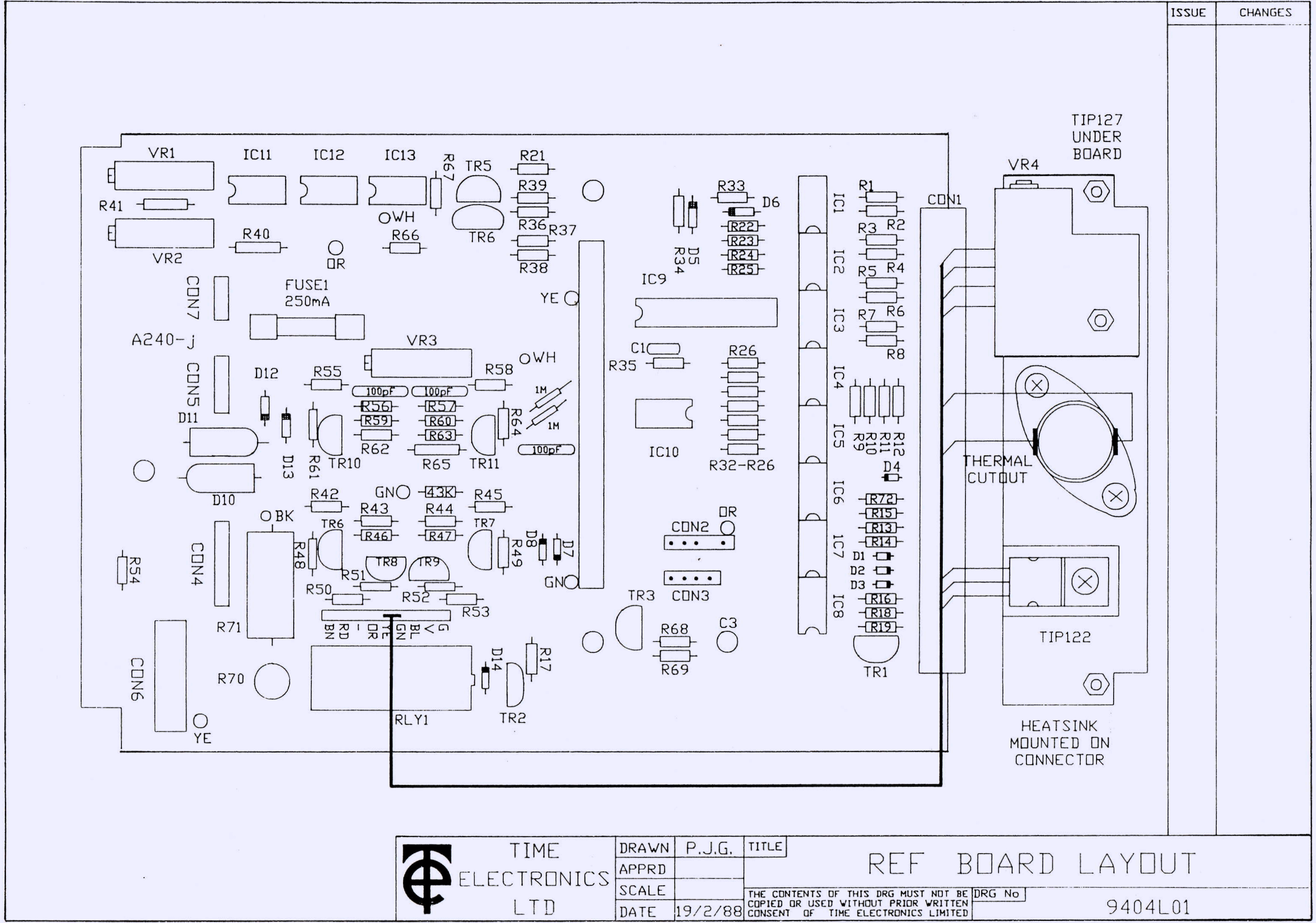
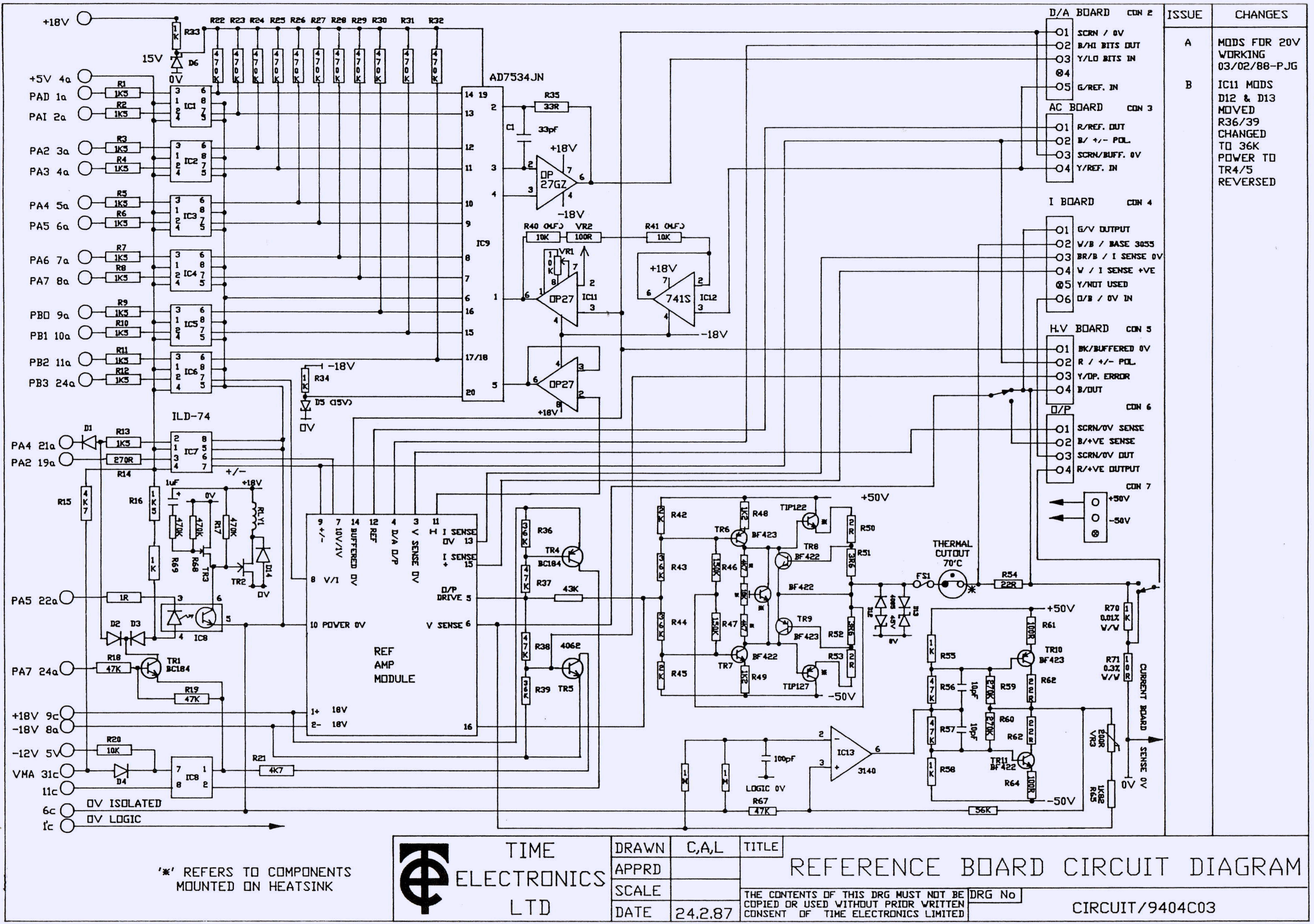
Reference assembly – A406-a

All the critical reference assembly is potted in black epoxy box, so it’s exact type of used voltage reference is still remain to be discovered. According to technical manual, there are two precision, aged zener diodes, running at optimum current. Output from these diodes is averaged and amplified to provide master reference voltage of +10.48576 VDC. There is also precision inverter inside potted assembly to provide -10.48576 VDC. This allows either positive or negative reference application, with help of low-thermal FET switch for analog output operation on either polarity.
Epoxy box pinout:
| Pin | Signal name | Purpose |
|---|---|---|
| 1 | +18V | Input power supply, positive |
| 2 | -18V | Input power supply, negative |
| 3 | V Sense 0V | Voltage sense, system common |
| 4 | D/A O/P | D/A module signal from DAC |
| 5 | O/P DRIVE | Drive output? |
| 6 | V SENSE | Sense line to positive output |
| 7 | 10/1V | Range selection input, 2/20V |
| 8 | V/I | Output selection, DCV or DCI |
| 9 | +/- | Polarity selection, pos/neg |
| 10 | Power 0V | Isolated ground reference 0V |
| 11 | H | Feedback to DAC? |
| 12 | REF | Reference output to AC board |
| 13 | I SENSE 0V | Current sense, system common |
| 14 | BUFFERED 0V | Buffered zero output |
| 15 | I Sense + | Current sense, positive output |
| 16 | No name | Feedback? |
Potted reference-amplifier module accepts ±18V input power supply from backplane connector and provides stable voltage or current reference for rest of the calibrator.
Reference output is fed into two D/A converters, both of them working in sync to form a composite 20-bit DAC. Least significant bits are formed by monolithic Analog Devices AD7534 14-bit DAC output. Six higher extra bits are added by separate D/A assembly board, which is discrete R2R logic using high-stability resistors and potted FET assembly. End result is 20-bit DAC code resolution converted into analog voltage. There is also substitute to Analog Devices DAC, MX7534 made by Maxim Integrated. Chip is still in production, even though it’s cost is over $30 USD.
1K&Omega R70 and 10Ω R71 form output voltage divider for 20 and 200mV voltage levels.
This board have whole array of no less than eight socketed dual-channel ILD74 optocouplers. Perhaps it’s used for trimming reference output?
Metal bar above the backplane connector have Honeywell 2455R type thermostat. Why it is located outside of reference block?
Block diagram:

Location map:
Schematics:
D/A module

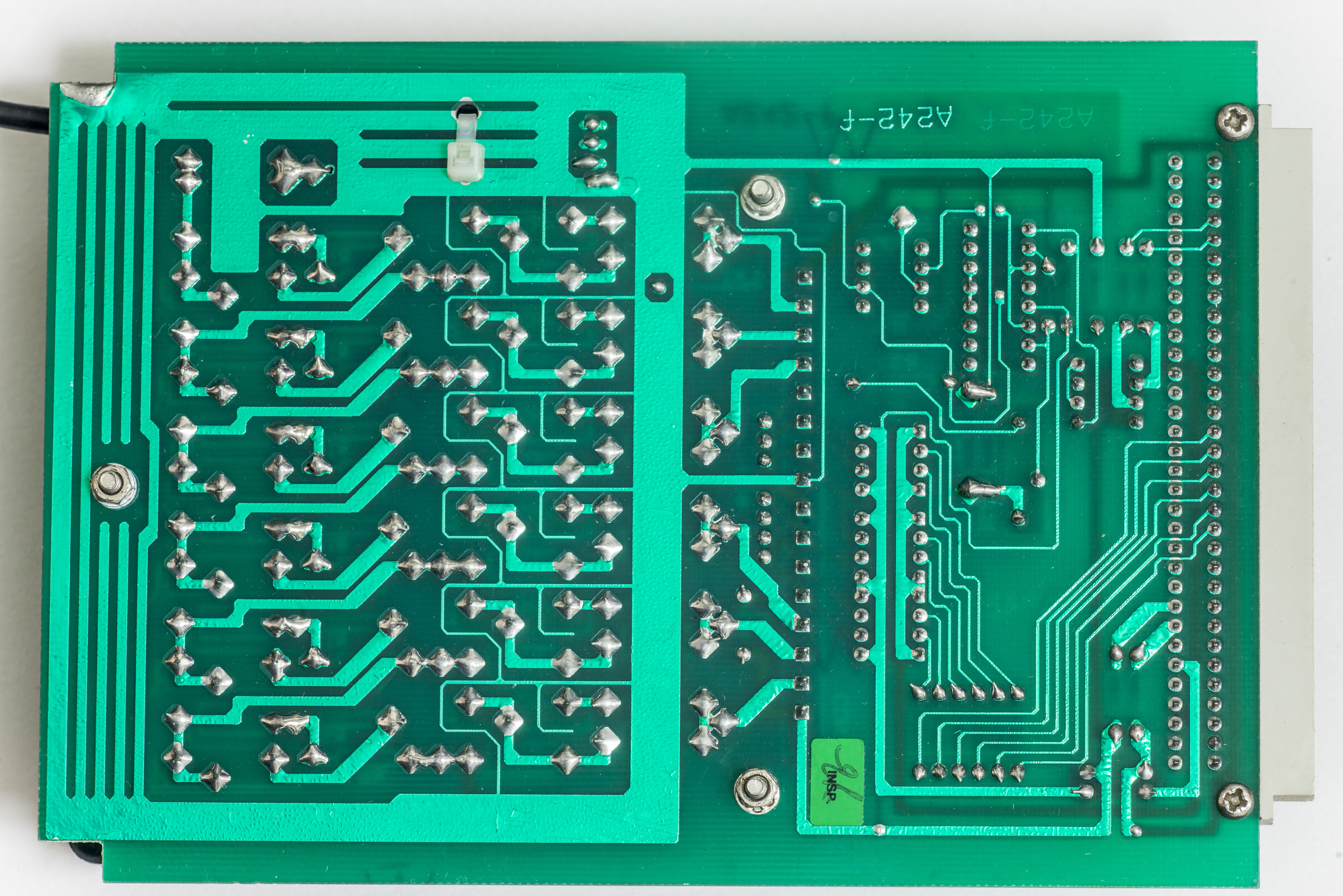
Similar to reference, D/A converter is potted in black epoxy box, marked 9823 D/A MODULE with serial code 1725 H9, whatever that means. It’s hard plastic, so there is little chance of taking it apart without damaging circuits inside.
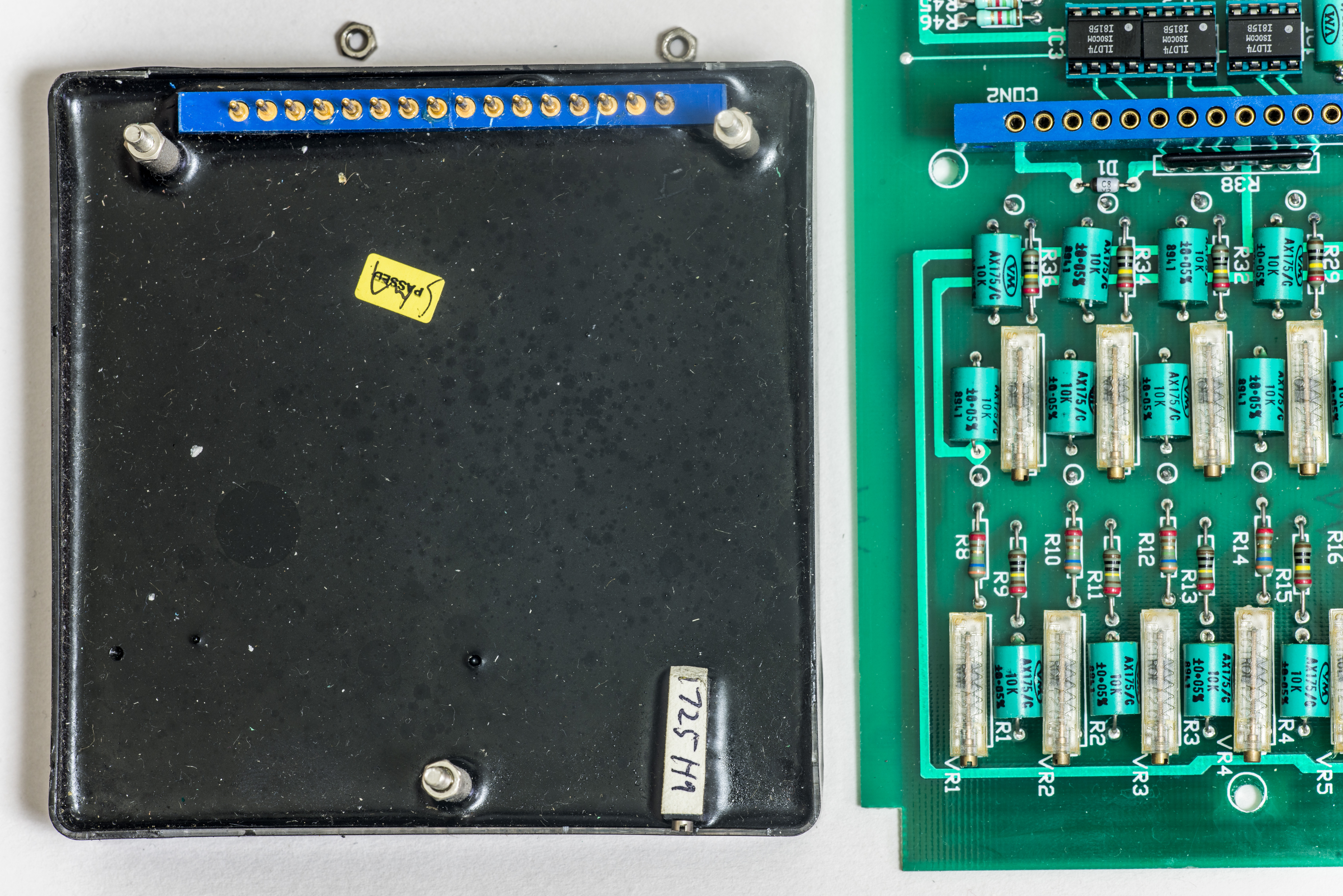
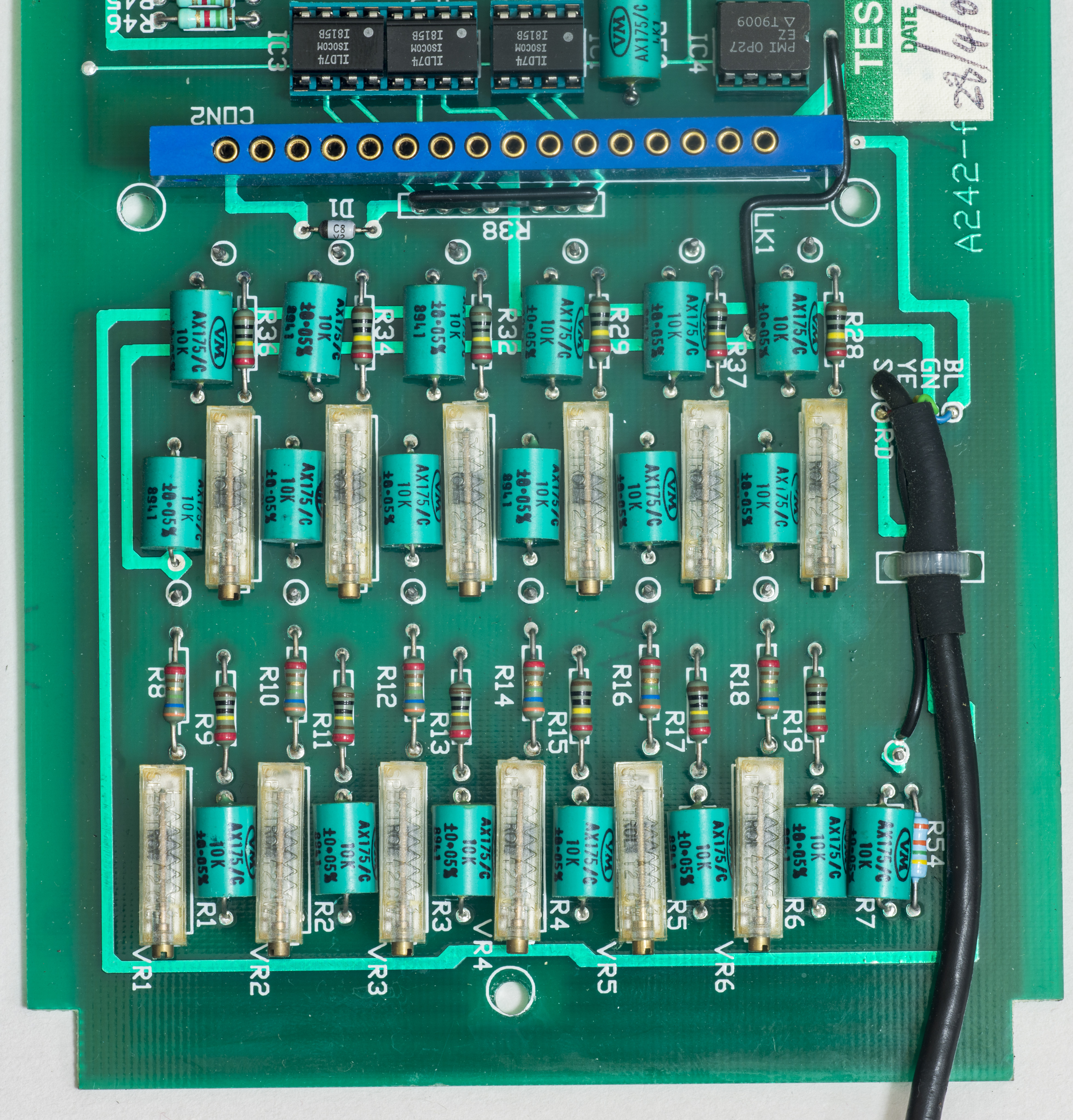
D/A PCB have array of 12 ultra-precision 3ppm/°C AX175/C wire-wound resistors paired with good quality trimmers. Perhaps this is to allow linearity adjustment, if DAC used have 12-bit resolution?
There is also Low-noise OP27 opamp, DG211 Quad SPST CMOS Analog Switch and four socketed dual-channel ILD74 optocouplers.
Interesting Vishay precision 10.000 KΩ R51 resistor located nearby with good collect gold-plated sockets at pins, paired with VR13. Perhaps gain adjustment?
Block diagram:

Encapsulated module have logic, buffer amplifiers and FET switches to convert digital code into analog output level.
R-2R resistor ladder consist of high quality, very low temperature coefficient resistors which have been carefully chosen, in resistance value and type, to provide best long-term stability. Value of each resistor is further trimmed with multi-turn pot to provide good linearity. Output of the ladder is buffered and fed back to reference board to be combined with LSB DAC output.
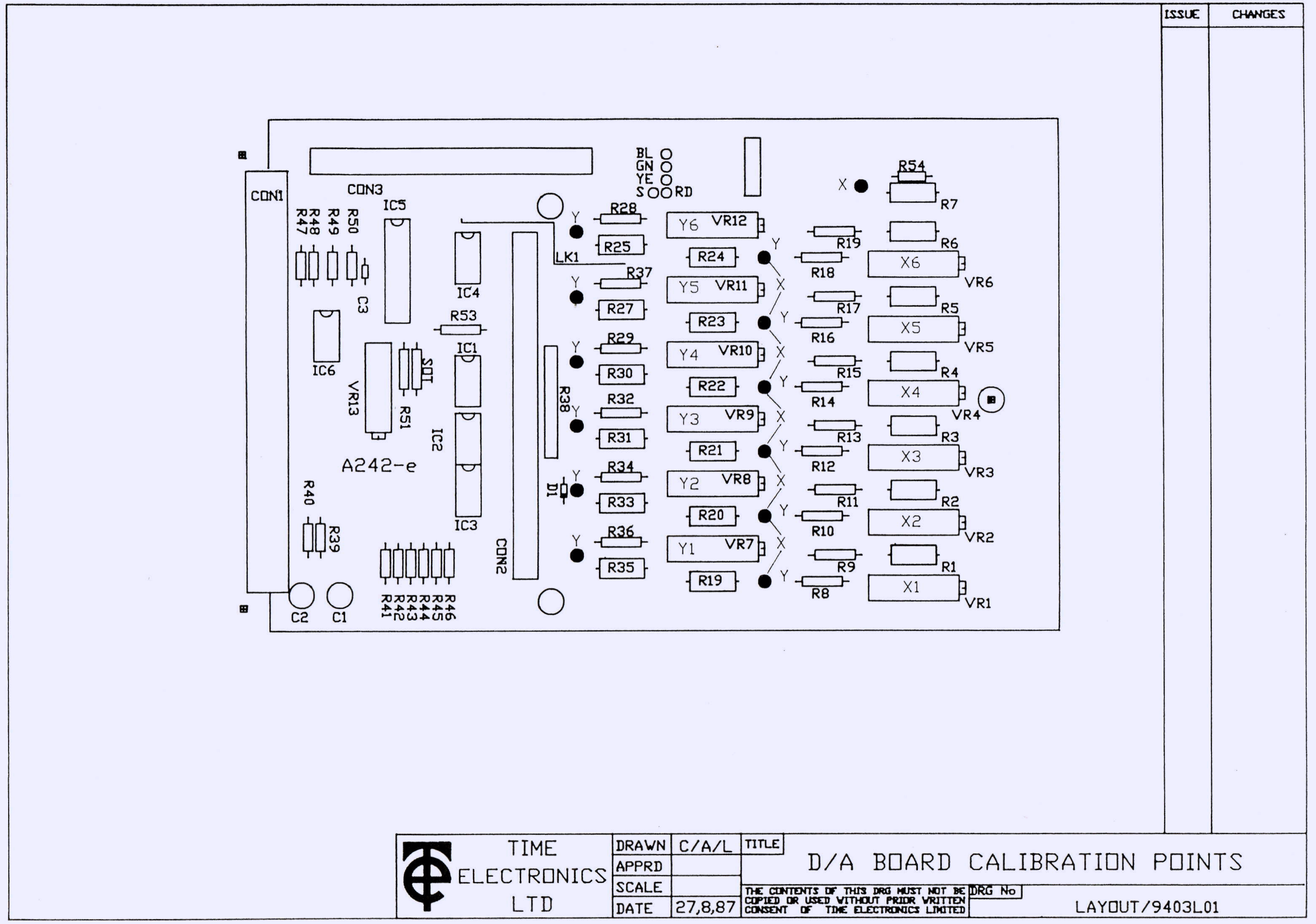
Calibration points:
D/A PCBA schematics:

Current output module – A246-j
This board located in slot position 34.
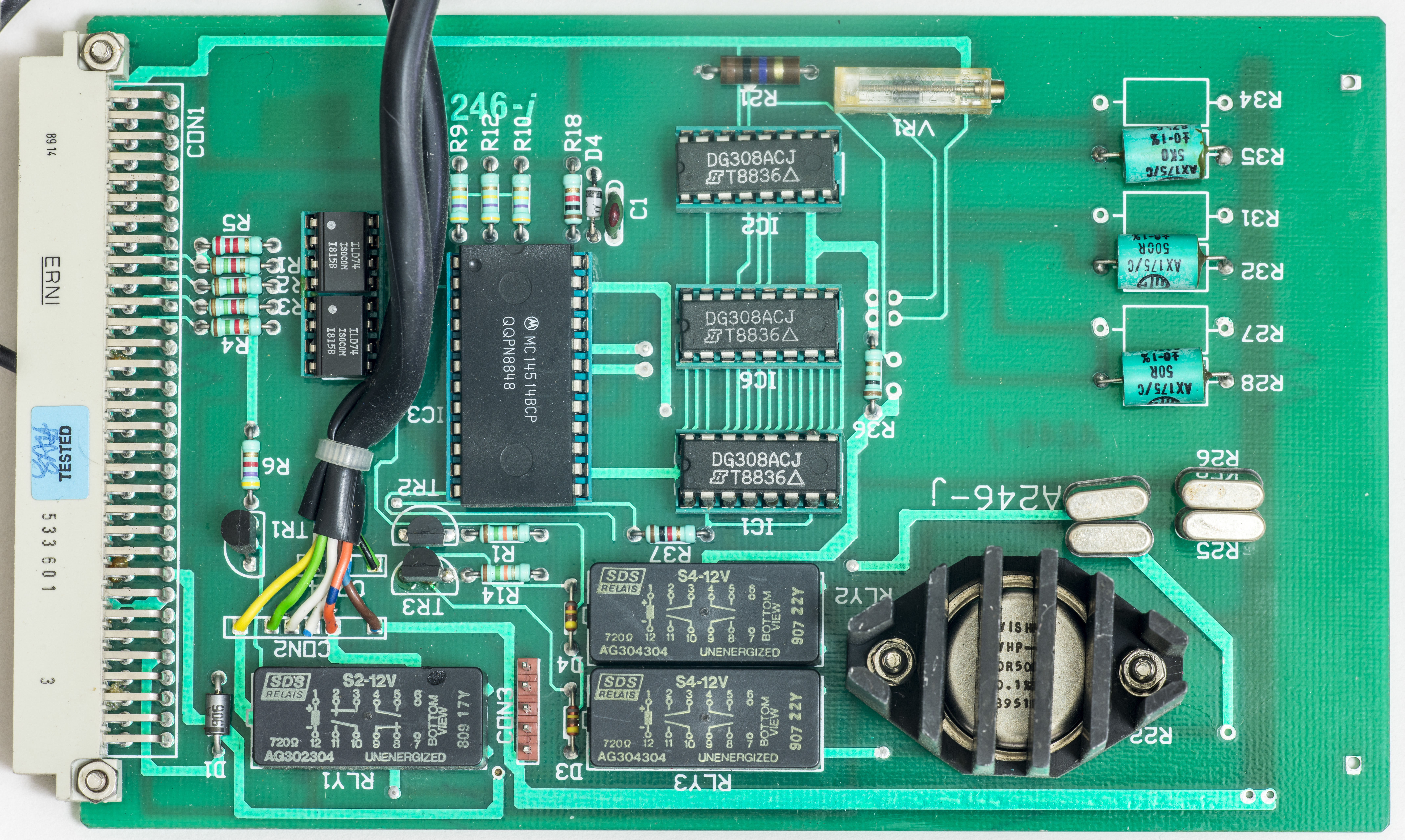

This board have MC14514B 4-bit latch/4-to-16 Decoder isolated by two socketed dual-channel ILD74 optocouplers. Current range switching is done via three Quad SPST analog switches DG308ACJ. Precision Vishay BMF resistors and 3ppm/°C AX175/C wire-wound resistors are used for best stability and long-term accuracy on current measurement.
Large foil resistor from Vishay, packaged in TO-3 4-wire package mounted to board with cast heatsink.
| RefDes | Resistance value | Resistor type | Measured | TCR |
|---|---|---|---|---|
| R22 | 10.5 Ω ±0.1% | VPG BMF Hermetic VHA | ? ppm/°C | |
| R25 | 5.0 Ω ±0.1% | VPG BMF Hermetic VHP202 | ? ppm/°C | |
| R26 | 5.0 Ω ±0.1% | VPG BMF Hermetic VHP202 | ? ppm/°C | |
| R28 | 50 Ω ±0.1% | AX175/C wire-wound resistors | 3ppm/°C | |
| R32 | 500 Ω ±0.1% | AX175/C wire-wound resistors | 3ppm/°C | |
| R35 | 5.0 KΩ ±0.1% | AX175/C wire-wound resistors | 3ppm/°C |
These resistors are used as current shunts for current ranges from 200µA to 2A and related 4-wire Kelvin connection circuitry. Three lower current ranges are switched by a FET switch, while higher current 200mA/2A ranges switched by relays. This module also provide control signal to 10A high-current board, located in front side of the instrument.
Cable CON3 wiring connection table:
| Pin | Signal name | Wire color/cable |
|---|---|---|
| 1 | ? | Red on PE white cable |
| 2 | ? | White on PE white cable |
| 3 | ? | Red on gray cable |
| 4 | ? | Blue on gray cable |
| 5 | ? | Black on PE white cable |
VR1 perhaps adjust current zero?
Resistance standard assembly – A337-g
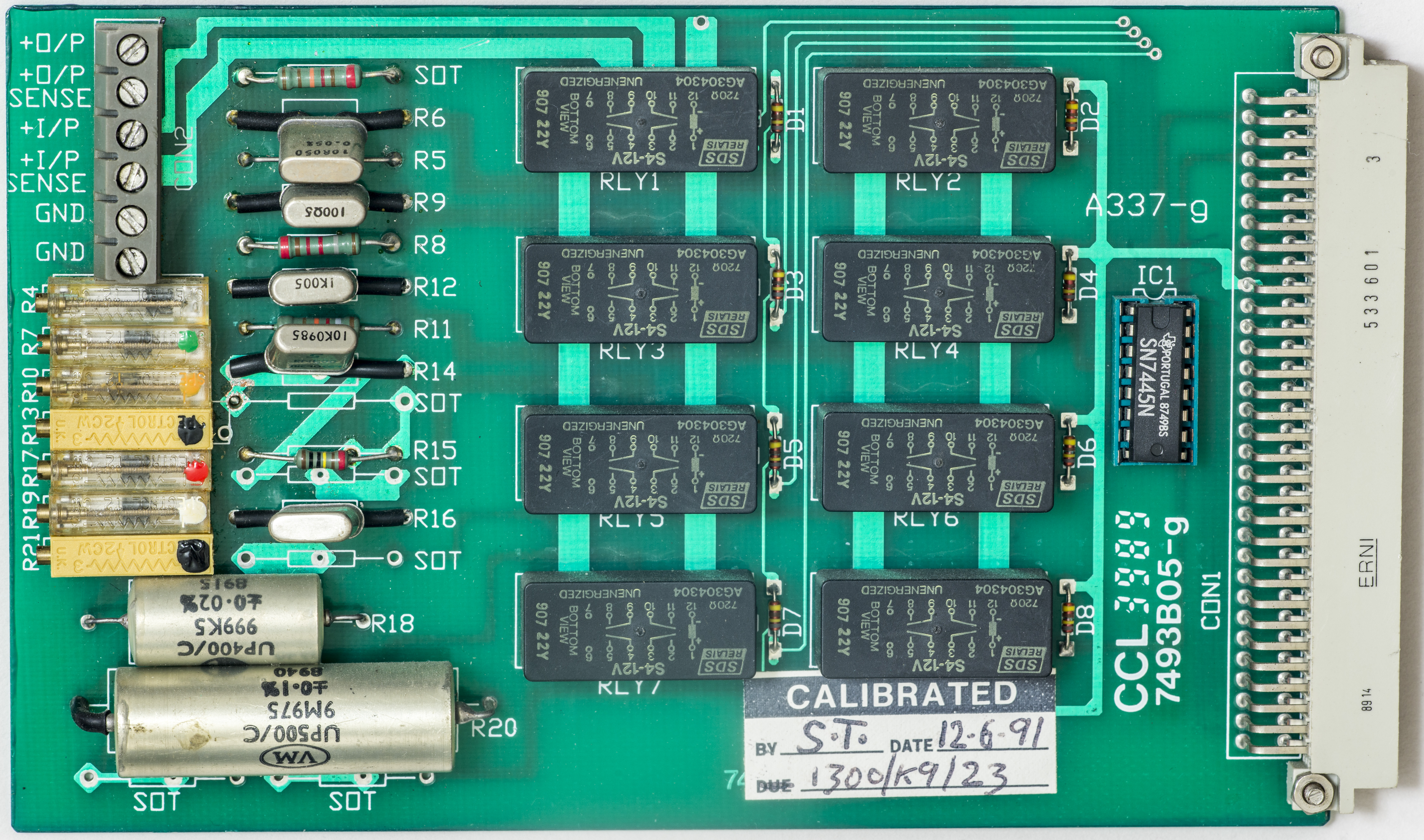
This assembly is resistance standard of calibrator. Even without schematics it’s operation is very easy to understand. SN7445N BCD-to-DECIMAL decoder switches on one of eight S4-12V relays, which are connecting one of reference resistors to 4-wire Kelvin output at CON2 terminal block or bypass these resistors for voltage/current output.
High-value resistors are nitrogen-filled 3ppm/°C UP400/UP500 with specified 15ppm/2000 hours long-term drift with thermal EMF less than 0.5µV/°C. This is really nice resistors here.
| RefDes | Resistance value | Resistor type | Measured | TCR |
|---|---|---|---|---|
| R6 | 10.050 Ω ±0.05% | VPG BMF Hermetic VHP202 | ? ppm/°C | |
| R9 | 100.5 Ω ± | Micro RNK00 BMF Hermetic | ? ppm/°C | |
| R12 | 1.005 KΩ ± | Micro RNK00 BMF Hermetic | ? ppm/°C | |
| R14 | 10.0985 KΩ ± | Micro RNK00 BMF Hermetic | ? ppm/°C | |
| R16 | 100 KΩ ± | VPG BMF Hermetic VHP | ? ppm/°C | |
| R18 | 999.5 KΩ ±0.02% | UP400 | 3 ppm/°C | |
| R20 | 9.975 MΩ ±0.1% | UP500 | 3 ppm/°C |
Cable CON2 wiring connection table:
| Pin | Signal name | Wire color/cable |
|---|---|---|
| 1 | +O/P | Red on PE white cable |
| 2 | SENSE | White on PE white cable |
| 3 | +I/P | Red on gray cable |
| 4 | SENSE | Blue on gray cable |
| 5 | GND | Black on PE white cable |
| 6 | GND | Black on gray cable |
Label on the board says it was calibrated by S.T. in 12 June 1991 to be used in 1300/K9/23 unit.
PCB itself was designed and manufactured in 1989, week 39.
AC waveform assembly – A394-h
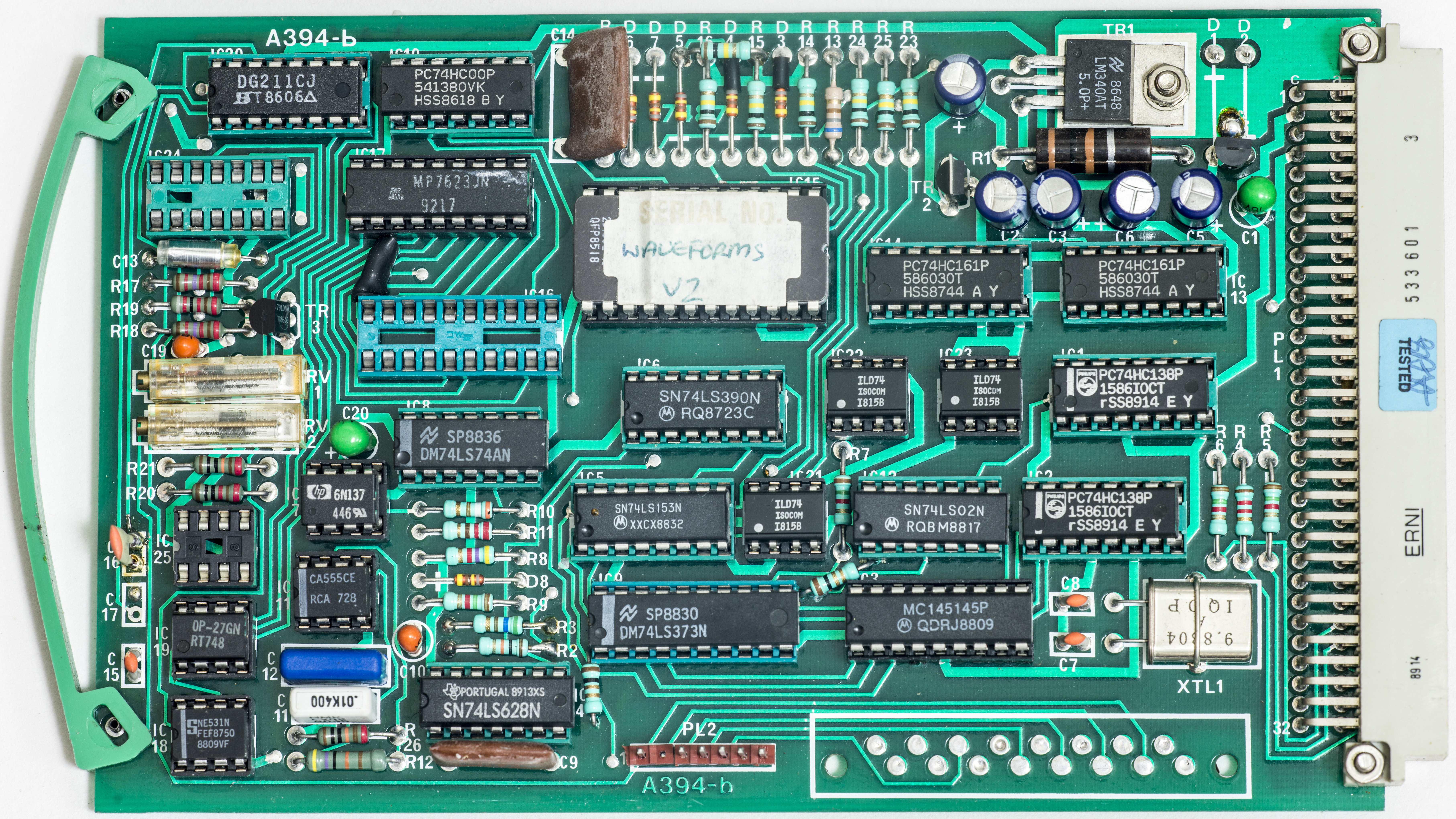

This complex board (compared to others) function as AC signal synthesizer, using UV EPROM as sample memory with waveform shapes. There are lot of logic, such as 74HC161 Synchronous 4-bit Binary Counters, 74HCT138 3-to-8 line decoder, few more dual-channel ILD74 optocouplers. Reference oscillator is based on MC145145P PLL Frequency Synthesizer with 4-bit data input. It takes 20MHz generated by SN74LS628N VCO as reference clock. Crystal oscillator nearby specified for frequency 9.8804MHz.
Board also features few “high-speed”, 1MHz NE531 opamps, 10MBd 6N137 logic optocoupler, resistor ladder 12-bit DAC MP7623, specified with 0.2ppm/°C max linearity.
Few IC sockets are empty, perhaps some options reserved for future use?
Local +5V power generated by LM340AT-5.0P in TO-220 package near mezzanine connector.
Mains power supply

High-voltage assembly
Mains power supply
Main power supply have 100VA low-frequency transformer, DC regulated supplies and circuitry for Local/Remote switch and some indicators.
Transformer has two 120VRMS primary windings and 9V, 11V and two 22VRMS secondary windings. 9V winding connects to a full-wave bridge rectifier and smoothing cap via 2A fuse. It supply regulated 5VDC with maximum loading 1A for digital circuitry, IEEE interface board and front panel display board.
Also additional full-wave rectifier provides unregulated 14VDC at 1A, to further provide 5V for relays drive and latching relays.
Pair of 22VRMS windings are rectified to supply ±28VDC and regulated ±18VDC for all the analog circuitry. 11V winding can be cascaded with 22V one to give unregulated ±50VDC for output stage of the calibrator DAC.
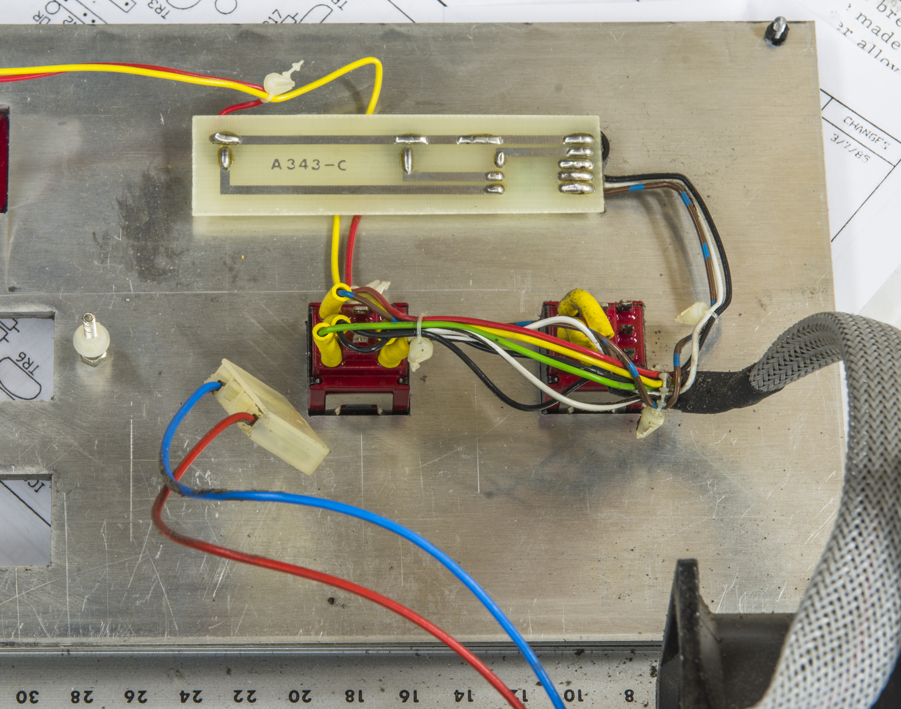
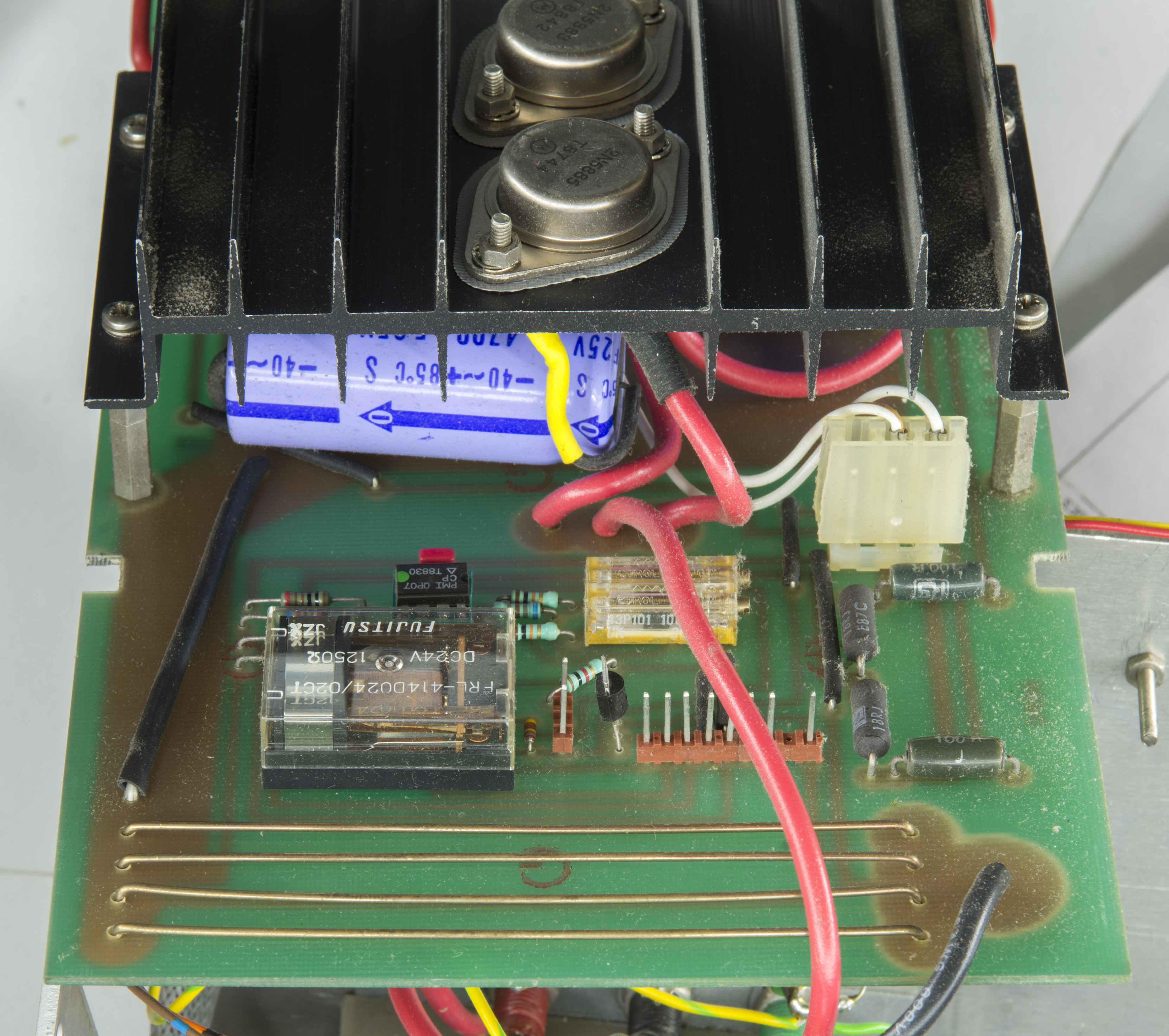
High current power amplifier

This board generates an unregulated voltage approximately ±4V to supply high-current source. This voltage is regulated by push-pull stage to provide up to 10Amps of current.
PA board with cables connected:
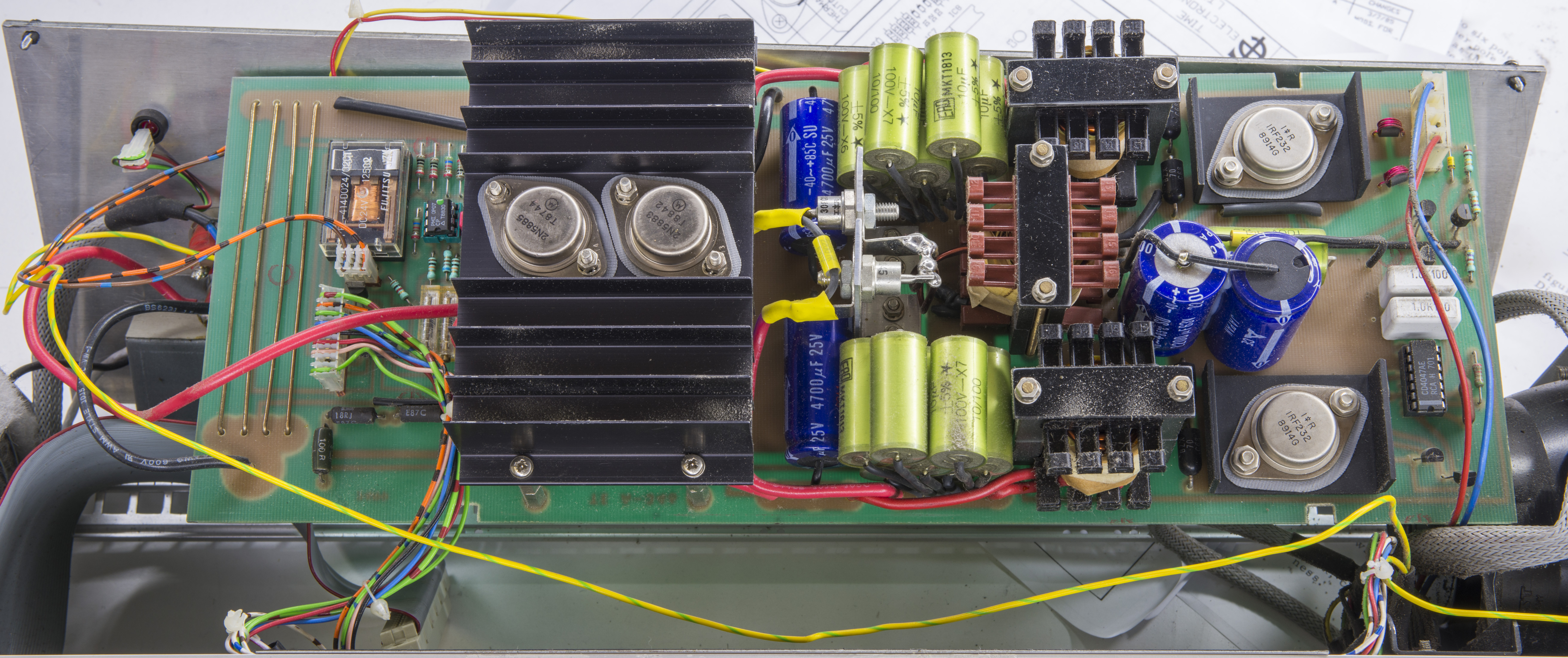
High-current shunt is formed with four long strands, perhaps from resistive material? According to technical manual, output current sense element is 0.01 Ω with kelvin connection. Voltage generated by sensor (0.1V at 10A, simple Ohm law) is amplified 10 times by a differential amplifier and provided back to Reference assembly sense I/P terminals to close the feedback loop and regulate current.
Overall construction

Firmware dumps
Main firmware, Model 9823, Version P23 – AM2764A UV EPROM
Calibration ROM dump, Model 9823 – EXEL XLS2816AP-250 ROM
Waveforms, Model 9823, Version 2 – TMS2516JL-45 UV EPROM
Repair workflow
Power supplies checked, working well. Optocouplers checked, all working, but really with slow rise-times, ~11-25µs. Should not be an issue, but worth to check.
Calibrator does turn on okay, front panel shows 9823 P23 message and operating at first glance normally, all buttons responsive, but output is not correct. Output does not match setting, and jumps in very big steps. E.g. setting 0.00000V on 10V range gives correct zero, but if setting increased to 1.00000V output jumps to 1.3612xxV. 1.10000V setting does not change output, still stays 1.3612xxV and only at 1.70000V setting output changes to 1.8531xxV. Similar situation happens on all other ranges. Current ranges giving OP ERROR message on front panel display, likely short of operation error?
I tried replacing old optocouplers with brand new Vishay ILD74’s but that help nothing, calibrator still had same issues with voltage output being adjusted in large steps only from MSB discrete DAC ladder.
Since all power supplies present and stable, voltage reference have stable output on REF module at -10.342xxx VDC, it does seem to me like digital/control issue. Knowing from teardown and schematics above – output is delivered from composite DAC, with 14-bit AD7534 being in charge for lowest 14-bits. I reseated all ICs, tried replacing OP27 op-amps with LT1007 around DAC on REF module, that did not change anything. ILD74 optocouplers were all checked using separate test jig with use of HP 33120A ARB, Keithley 2304 PSU and Tektronix CSA7404 scope.
There is not much else going on reference board module, that quickly made DAC chip itself to main suspect. I ordered a replacement AD7534 from UTSource store (which often have many obsolete/rare parts) to test this theory. New chip arrived 29/March/2016, with date code 38 week 2012 in little box with anti-static bag.
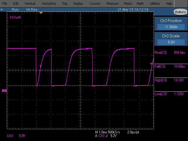
Replacement of DAC chip did not change anything though, so we back to digital debug. To see what is DAC chip receiving, TLA714 Logic analyzer was hooked to data bus, A0,A1 and CS/WR signals at the DAC board.
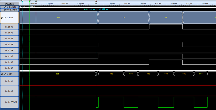
During change of output setting from FP keypad, processor sends four bytes to DAC. All 8 bits of data bus (D[0:7]) work fine, CS/WR (tried together at board) work fine too, latching data by rising edge, but the A0 and A1 signals stay dead low no matter how many times I tried to adjust setting. According to MX7534 datasheet this makes direct DAC register load. And since last transaction is with databus set to all zero, it sets DAC output to zero every time, not the correct value.
This brings us to processor board. All the interfacing to analog side is done from pair of MC6832 PIA controllers. Swapping them on processor board made A0/A1 and CS toggle continuously, while D[0:7] bus stay dead low at all times. Perhaps one of PIAs is dead, as these controllers don’t have any internal ROM to explain difference in operation. They are rather simple I/O and IRQ registers for processor bus. Ordered pair of chips from eBay, will see what that does.
Ok, I got the Motorola 68A21P replacement in the board, let’s see what it brings us. A0/A1 signals are present at the DAC now, so control lines and data bus is working correctly now. Here’s how signaling should look:
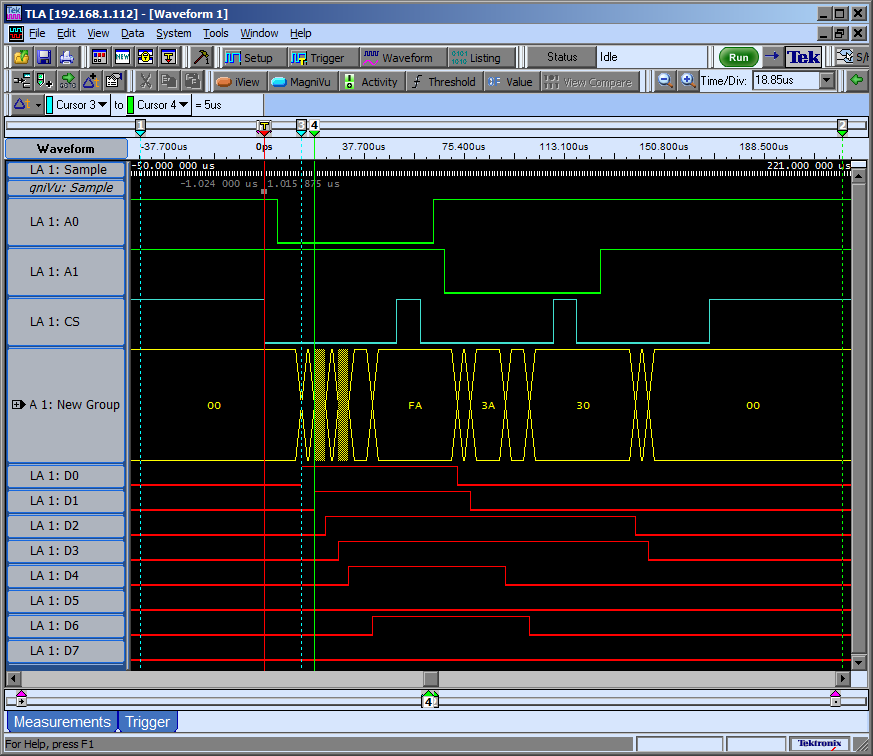
And since I wanted to get faster rise/fall times out of optocouplers just in case, 100KΩ pull-up resistors on DAC’s digital lines (ones marked 470K on schematics) were replaced as well with 20KΩ which gives almost 1mA of transistor current. Output I-V amplifier on AD7534 output is Linear LT1007CN8, which was tested and confirmed working on separate test jig.
And here’s our progress:
You can see output on calibrator set to 20.00000 VDC and it’s indeed very close to that measured on three Keithley DMMs around (not calibrated). Next step would be full testing of all ranges and functions, to make sure everything works. Once that is done, calibrator will be fully assembled with all covers to perform few days warmup to get all components settled and calibration will be done, using HP 3458A.
Worth to note, that replacement AD7534JN is broken or counterfeit, as it was not working even on the test jig, and VSS pin was constantly loading it’s supply below -11VDC, while original DAC from Time 9823 have this pin steady at zener’s -14.8VDC.
Here are photos of both sides of fake DAC:
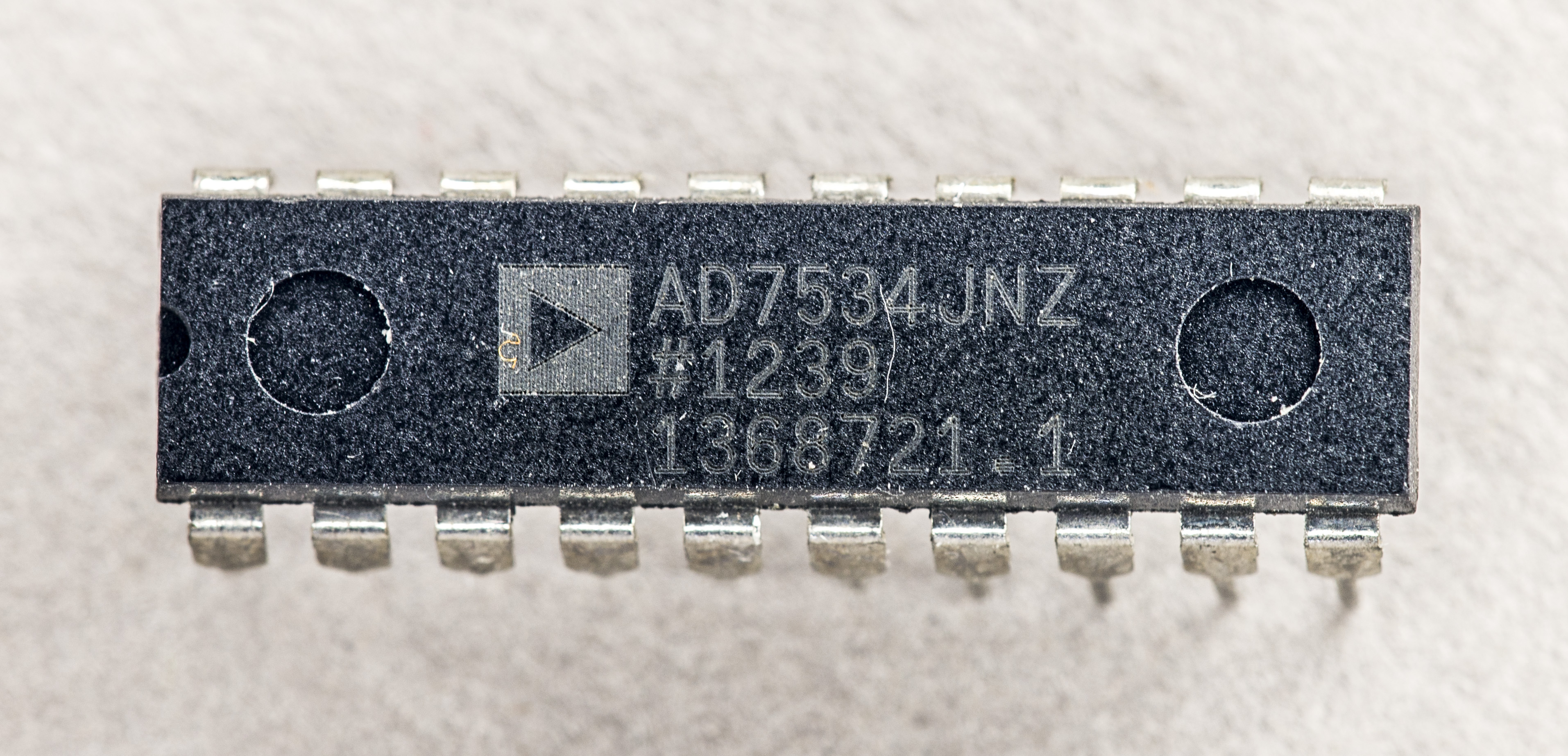
Marking look legit to me, it’s nice quality laser etch, just like I see on some other genuine Analog Devices components. Buyers – always beware expensive components with really low prices ;). It’s often worth to spend 20$USD more and save lot of time wondering if part is good or not.
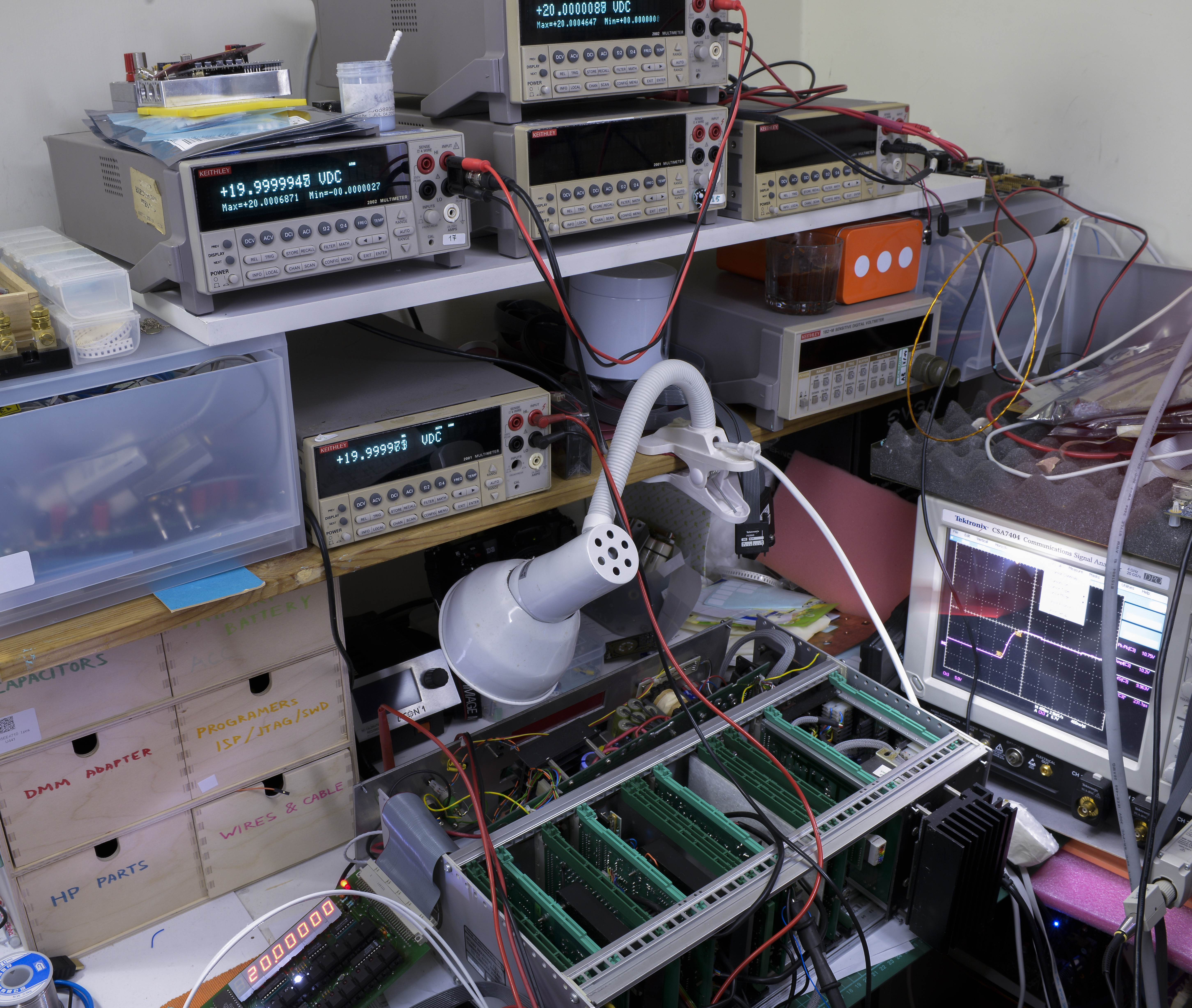
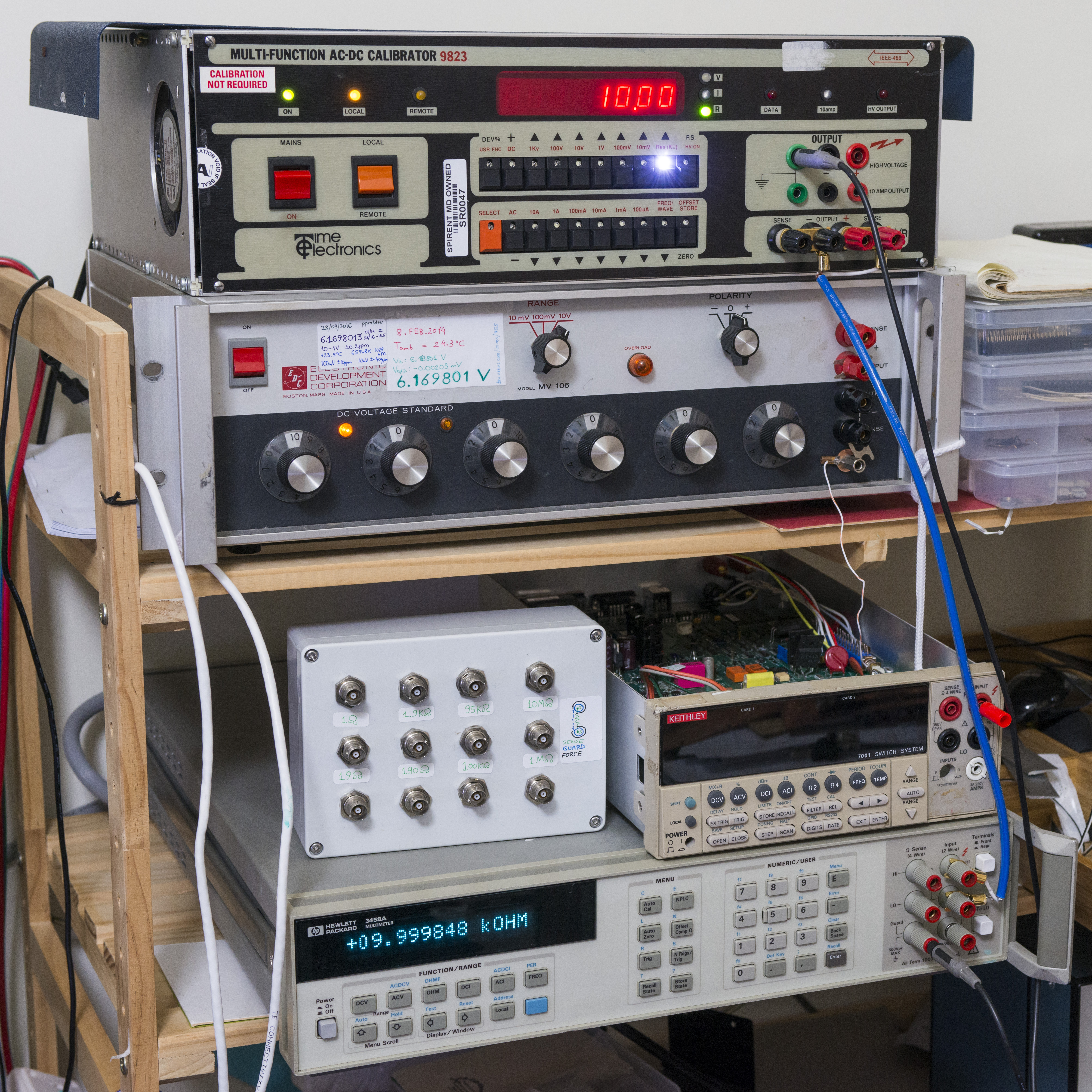
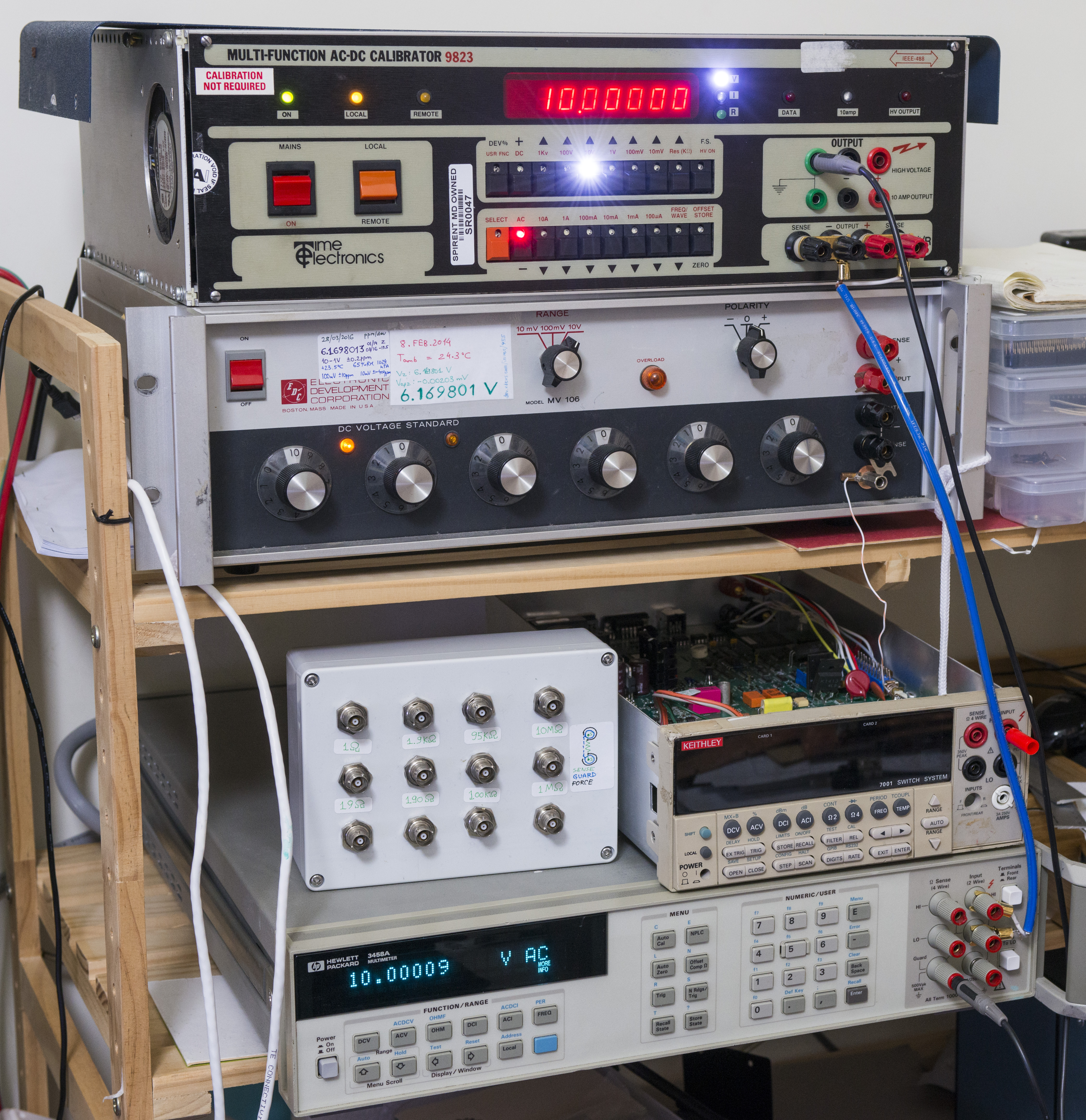
Currently MFC running 10.0000V output, connected to DMM for logging to check if it’s stable.

Tempco of the output voltage seem to be -1.9ppm/°C which is bit high, but actually fits specifications of ±2ppm/°C. We will be checking later if it’s possible to improve stability and reduce temperature sensitivity. For comparison, industry standard multifunction calibrators, such as Fluke 5700A offering ±0.24ppm/°C at 10VDC, in 10°C to 40°C window (22VDC specification ±0.2ppm/°C + 0.4µV).
Unit is being assembled and getting ready for some tests. You can actually really see how small this calibrator is, compared to other beasts of this instruments type, such as Fluke 55xx/57xx or Datron 4700/4800 series.

Calibration
According to calibration manual, most of its calibration data factors (both zero and full scale) is stored in nonvolatile EEPROM memory chip located on the Processor board. The calibration factors are stored twice in memory and when the unit is switched on the 2 sets are compared to check for corruption. Great idea, I’d say, no this Dallas NVRAM stuff with dying batteries, and that’s 10 years before Keithley 2001/2002 and about same time as HP 3458A were designed. This is something, as well as storing two copies, worth to learn from!
To be fair though, unlike Keithley Model 200x or HP 3458A DMMs, this calibrator still have some of the calibration adjustment done using old-school multi-turn trimmers which are mounted on the circuit boards. While older technical manual recommends use of Solartron 7081/7071 or Datron 1071/1081, latest calibration manual recommends HP 3458A, which I will be using.
Summary
| Qty | Part Number | Description | Price USD | |
|---|---|---|---|---|
| 20 | 160-1782-ND | LED WHITE CLEAR 3MM ROUND T/H | 9823 | 8.40 |
| 2 | 67-1696-ND | LED WHITE DIFF 5MM ROUND T/H | 9823 | 3.58 |
| 10 | 160-1684-ND | LED GRN DIFF 5MM ROUND T/H | 9823 | 2.85 |
| 5 | 754-1889-ND | LED YELLOW DIFF 5MM ROUND T/H | 9823 | 3.50 |
| 10 | VAOL-5LSBY1-ND | LED BLUE DIFF 5MM ROUND T/H | 9823 | 4.56 |
| 10 | 67-1648-ND | LED RED DIFF 5MM ROUND T/H | 9823 | 3.78 |
| 10 | 754-1604-ND | LED RED CLEAR 3MM ROUND T/H | 9823 | 2.70 |
| 1 | AD7534JN | DAC 14-bit Parallel current | UTsource | 8.0 |
| 2 | Motorola M68A21P PIA | Parallel Interface controller | eBay | 15.0 |
Testing and performance
Resistance standard function.
Below are test samples in ambient temperature environment, measured by HP 3458A.
Configuration settings in python app:
# Setup HP 3458A
self.inst.clear()
self.inst.write("PRESET NORM")
self.inst.write("OFORMAT ASCII")
self.inst.write("OHMF 100")
self.inst.write("TARM HOLD")
self.inst.write("TRIG AUTO")
self.inst.write("NPLC 100")
self.inst.write("AZERO ON")
self.inst.write("OCOMP ON")
self.inst.write("LFILTER ON")
self.inst.write("NRDGS 1,AUTO")
self.inst.write("MEM OFF")
self.inst.write("END ALWAYS")
self.inst.write("NDIG 9")
self.inst.write("DELAY 3") # 3 second delay to mitigate OCOMP accuracy issue due DA
Test data and results for each range:
| Measured output | Test data and DSV-files | Condition | Measured resistance | TCR |
|---|---|---|---|---|
| Time 9823 MFC, 10Ω output | Test data graph | ambient | Ω | ppm/K |
| Time 9823 MFC, 100Ω output | Test data graph | ambient | 99.96981 Ω | +1.2 ppm/K |
| Time 9823 MFC, 1KΩ output | Test data graph | ambient | 999.690 Ω | -0.42 ppm/K |
| Time 9823 MFC, 10KΩ output | Test data graph | ambient | 9999.425 Ω | -0.92 ppm/K |
| Time 9823 MFC, 100KΩ output | Test data graph | ambient | 99997.26292 Ω | +1.5 ppm/K |
| Time 9823 MFC, 1MΩ output | Test data graph | ambient | 1000085.761 Ω | +1.93 ppm/K |
| Time 9823 MFC, 10MΩ output | Test data graph | ambient | 10010405.504 Ω | +4.3 ppm/K |
To be done soon, stay tuned.
Linearity testing
One of important specifications of any arbitrary source and generator is linearity. Accuracy of the output is not constant over the range of calibrator for every specific value setting. And since calibration is performed only on the zero and full-scale outputs, everything in between will depend on linearity error, well as other factors.
Knowing DAC architecture of this calibrator, we can easily come up with smallest possible step in output voltage programming, which is for used 20-bit DAC is equal roughly 1.9 µV (20V range / 220). Now we can perform a test, programming output with aligned values and measuring output with more linear instrument than Time 9823. Such a magic device is well known HP 3458A DMM with linearity specification <0.1ppm.
Raspberry Pi with linux-gpib was used to control both HP 3458A and Time 9823.
Summary
I would also like to give credits to:
- Marc C. at Telford Electronics shop for Time Electronics 9823 Technical manual,
- Joe D. for schematics pages and information on 982x calibrators
- Todd M. for overall support on project and patience to listen thru all the ramble :)
Projects like this are born from passion and a desire to share how things work. Education is the foundation of a healthy society - especially important in today's volatile world. xDevs began as a personal project notepad in Kherson, Ukraine back in 2008 and has grown with support of passionate readers just like you. There are no (and never will be) any ads, sponsors or shareholders behind xDevs.com, just a commitment to inspire and help learning. If you are in a position to help others like us, please consider supporting xDevs.com’s home-country Ukraine in its defense of freedom to speak, freedom to live in peace and freedom to choose their way. You can use official site to support Ukraine – United24 or Help99. Every cent counts.
Modified: Jan. 26, 2018, 11:17 a.m.